WO2011102020A1 - スイッチモジュール - Google Patents
スイッチモジュール Download PDFInfo
- Publication number
- WO2011102020A1 WO2011102020A1 PCT/JP2010/069149 JP2010069149W WO2011102020A1 WO 2011102020 A1 WO2011102020 A1 WO 2011102020A1 JP 2010069149 W JP2010069149 W JP 2010069149W WO 2011102020 A1 WO2011102020 A1 WO 2011102020A1
- Authority
- WO
- WIPO (PCT)
- Prior art keywords
- light
- light guide
- guide member
- key
- switch module
- Prior art date
- Legal status (The legal status is an assumption and is not a legal conclusion. Google has not performed a legal analysis and makes no representation as to the accuracy of the status listed.)
- Ceased
Links
Images


Classifications
-
- H—ELECTRICITY
- H01—ELECTRIC ELEMENTS
- H01H—ELECTRIC SWITCHES; RELAYS; SELECTORS; EMERGENCY PROTECTIVE DEVICES
- H01H13/00—Switches having rectilinearly-movable operating part or parts adapted for pushing or pulling in one direction only, e.g. push-button switch
- H01H13/70—Switches having rectilinearly-movable operating part or parts adapted for pushing or pulling in one direction only, e.g. push-button switch having a plurality of operating members associated with different sets of contacts, e.g. keyboard
- H01H13/83—Switches having rectilinearly-movable operating part or parts adapted for pushing or pulling in one direction only, e.g. push-button switch having a plurality of operating members associated with different sets of contacts, e.g. keyboard characterised by legends, e.g. Braille, liquid crystal displays, light emitting or optical elements
-
- H—ELECTRICITY
- H01—ELECTRIC ELEMENTS
- H01H—ELECTRIC SWITCHES; RELAYS; SELECTORS; EMERGENCY PROTECTIVE DEVICES
- H01H9/00—Details of switching devices, not covered by groups H01H1/00 - H01H7/00
-
- H—ELECTRICITY
- H01—ELECTRIC ELEMENTS
- H01H—ELECTRIC SWITCHES; RELAYS; SELECTORS; EMERGENCY PROTECTIVE DEVICES
- H01H13/00—Switches having rectilinearly-movable operating part or parts adapted for pushing or pulling in one direction only, e.g. push-button switch
- H01H13/02—Details
- H01H13/023—Light-emitting indicators
-
- H—ELECTRICITY
- H01—ELECTRIC ELEMENTS
- H01H—ELECTRIC SWITCHES; RELAYS; SELECTORS; EMERGENCY PROTECTIVE DEVICES
- H01H13/00—Switches having rectilinearly-movable operating part or parts adapted for pushing or pulling in one direction only, e.g. push-button switch
- H01H13/70—Switches having rectilinearly-movable operating part or parts adapted for pushing or pulling in one direction only, e.g. push-button switch having a plurality of operating members associated with different sets of contacts, e.g. keyboard
- H01H13/88—Processes specially adapted for manufacture of rectilinearly movable switches having a plurality of operating members associated with different sets of contacts, e.g. keyboards
-
- G—PHYSICS
- G02—OPTICS
- G02B—OPTICAL ELEMENTS, SYSTEMS OR APPARATUS
- G02B6/00—Light guides; Structural details of arrangements comprising light guides and other optical elements, e.g. couplings
- G02B6/0001—Light guides; Structural details of arrangements comprising light guides and other optical elements, e.g. couplings specially adapted for lighting devices or systems
- G02B6/0011—Light guides; Structural details of arrangements comprising light guides and other optical elements, e.g. couplings specially adapted for lighting devices or systems the light guides being planar or of plate-like form
- G02B6/0033—Means for improving the coupling-out of light from the light guide
- G02B6/0035—Means for improving the coupling-out of light from the light guide provided on the surface of the light guide or in the bulk of it
- G02B6/004—Scattering dots or dot-like elements, e.g. microbeads, scattering particles, nanoparticles
- G02B6/0043—Scattering dots or dot-like elements, e.g. microbeads, scattering particles, nanoparticles provided on the surface of the light guide
-
- G—PHYSICS
- G02—OPTICS
- G02B—OPTICAL ELEMENTS, SYSTEMS OR APPARATUS
- G02B6/00—Light guides; Structural details of arrangements comprising light guides and other optical elements, e.g. couplings
- G02B6/0001—Light guides; Structural details of arrangements comprising light guides and other optical elements, e.g. couplings specially adapted for lighting devices or systems
- G02B6/0011—Light guides; Structural details of arrangements comprising light guides and other optical elements, e.g. couplings specially adapted for lighting devices or systems the light guides being planar or of plate-like form
- G02B6/0033—Means for improving the coupling-out of light from the light guide
- G02B6/0058—Means for improving the coupling-out of light from the light guide varying in density, size, shape or depth along the light guide
- G02B6/006—Means for improving the coupling-out of light from the light guide varying in density, size, shape or depth along the light guide to produce indicia, symbols, texts or the like
-
- G—PHYSICS
- G02—OPTICS
- G02B—OPTICAL ELEMENTS, SYSTEMS OR APPARATUS
- G02B6/00—Light guides; Structural details of arrangements comprising light guides and other optical elements, e.g. couplings
- G02B6/0001—Light guides; Structural details of arrangements comprising light guides and other optical elements, e.g. couplings specially adapted for lighting devices or systems
- G02B6/0011—Light guides; Structural details of arrangements comprising light guides and other optical elements, e.g. couplings specially adapted for lighting devices or systems the light guides being planar or of plate-like form
- G02B6/0065—Manufacturing aspects; Material aspects
-
- H—ELECTRICITY
- H01—ELECTRIC ELEMENTS
- H01H—ELECTRIC SWITCHES; RELAYS; SELECTORS; EMERGENCY PROTECTIVE DEVICES
- H01H2219/00—Legends
- H01H2219/036—Light emitting elements
- H01H2219/044—Edge lighting of layer
-
- H—ELECTRICITY
- H01—ELECTRIC ELEMENTS
- H01H—ELECTRIC SWITCHES; RELAYS; SELECTORS; EMERGENCY PROTECTIVE DEVICES
- H01H2219/00—Legends
- H01H2219/036—Light emitting elements
- H01H2219/046—Light emitting elements above switch site
-
- H—ELECTRICITY
- H01—ELECTRIC ELEMENTS
- H01H—ELECTRIC SWITCHES; RELAYS; SELECTORS; EMERGENCY PROTECTIVE DEVICES
- H01H2219/00—Legends
- H01H2219/054—Optical elements
- H01H2219/056—Diffuser; Uneven surface
-
- H—ELECTRICITY
- H01—ELECTRIC ELEMENTS
- H01H—ELECTRIC SWITCHES; RELAYS; SELECTORS; EMERGENCY PROTECTIVE DEVICES
- H01H2219/00—Legends
- H01H2219/054—Optical elements
- H01H2219/06—Reflector
-
- H—ELECTRICITY
- H01—ELECTRIC ELEMENTS
- H01H—ELECTRIC SWITCHES; RELAYS; SELECTORS; EMERGENCY PROTECTIVE DEVICES
- H01H2219/00—Legends
- H01H2219/054—Optical elements
- H01H2219/062—Light conductor
-
- H—ELECTRICITY
- H01—ELECTRIC ELEMENTS
- H01H—ELECTRIC SWITCHES; RELAYS; SELECTORS; EMERGENCY PROTECTIVE DEVICES
- H01H2229/00—Manufacturing
- H01H2229/02—Laser
Definitions
- the present invention relates to a switch module provided to face a key substrate of an electronic device such as a mobile phone or a notebook PC.
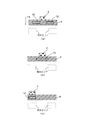
- FIG. 4 is a schematic perspective view of a conventional switch module 100 arranged to face a key substrate 80 having a plurality of key portions 70.
- FIG. 5 is a schematic sectional view of the switch module 100 shown in FIG.
- the switch module 100 is provided with a metal dome 50 that encloses an electrode 55, a circuit board 60, a light guide member 30, and an LED (LightLEDEmitting Diode) 20 as a light emitting element.
- the metal dome 50 is integrally held on the circuit board 60 by the metal dome sheet 40, and the light guide member 30 is attached to the metal dome sheet 40 at a predetermined interval by the adhesive layer 35.
- the light guide member 30 is provided with a light scattering processing portion 30a such as a printing process in which white ink is printed in the form of dots or a prism process on the lower surface of the light guide member 30, and between the light guide member 30 and the LED 20.
- a reflector (reflective member) 25 for efficiently guiding light emitted from the LED 20 from the end of the light guide member 30 into the light guide member 30 is provided.
- the end portion of the reflector 25 extends to a position that covers the upper surface of the light guide member 30.
- the switch can be turned on and off by electrical contact or non-contact between the metal dome 50 and the electrode 55 due to the key portion 70 being pressed downward and the metal dome 50 being deformed. Since the light guide member 30 is provided on the back surface of the key substrate 80, that is, between the key substrate 80 and the metal dome sheet 40, the light emitted from the LED 20 and entering the light guide member 30 is reduced. Each key portion 70 can be illuminated from within the light guide member 30 by being scattered by the light scattering processing portion 30a. Related techniques are disclosed in Patent Documents 1 to 6.
- Patent Document 1 Japanese Patent Application Laid-Open No. 2009-246821
- Patent Document 2 Japanese Patent Application Laid-Open No. 2008-152951
- Patent Document 3 Japanese Patent Application Laid-Open No. 2009-140871
- Patent Document 4 Japanese Patent Application Laid-Open No. 2009-187855
- Patent Document 5 Japanese Patent Application Laid-Open No. 2009-187855 Japanese Patent Laid-Open No. 2004-139983
- Patent Document 6 Japanese Patent Laid-Open No. 2008-226844
- FIG. 5B schematically shows the traveling direction of light in the light guide member 30.
- Light emitted from the LED 20 and incident into the light guide member 30 from the end of the light guide member 30 by the reflector 25 is repeatedly reflected on the upper and lower surfaces of the light guide member 30, for example, as indicated by L ⁇ b> 1 in the drawing.
- the light guide member 30 is advanced.
- the light incident on the light guide member 30 is guided in the vicinity of the edge portion of the reflector 25 even though the light scattering processed portion 30a is not formed like the light indicated by L3 and L4 in the drawing.
- the area where the light of L3 and L4 leaks out that is, the area near the LED 20 is excessively light as compared with other areas.
- a switch module that can illuminate a key part has a requirement of “luminance uniformity” such that a plurality of key parts are illuminated with as uniform luminance as possible.
- luminance uniformity such that a plurality of key parts are illuminated with as uniform luminance as possible.
- the present invention reduces the amount of light leaking from the vicinity of the edge portion of the reflector toward the key portion in the switch module provided facing the key substrate, and makes the key portion uniform by the light traveling in the light guide member.
- An object is to provide a switch module that can be illuminated.
- the present invention provides: A switch module provided opposite to a key board having a key part, A circuit board having an electrode layer formed on a surface facing the key board; A light guide member provided between the key board and the circuit board; A light source element that emits light; A reflection member that causes light emitted from the light source element to enter the light guide member from an end of the light guide member; With A switch that can be turned on and off by moving the key portion relative to the electrode layer, and that can illuminate the key portion from within the light guide member by light incident on the light guide member.
- the light guide member has a first surface facing the key substrate and a second surface on the opposite side and facing the circuit substrate, and the reflection member is a first surface at the end portion.
- the light scattering processing for reducing the amount of light is performed on the optical path of the light transmitted through the first surface from the vicinity of the edge portion of the reflecting member, so that the edge portion of the reflecting member is provided.
- the amount of light leaking from the vicinity can be reduced.
- the light scattering processing for dimming is formed only on the optical path of light leaking from the vicinity of the edge portion of the reflecting member. Therefore, the other light traveling through the light guide member (light that does not leak from the vicinity of the edge portion) can be sufficiently illuminated without being scattered by the light scattering processing for dimming.
- the light incident on the light guide member is scattered, and light scattering processing for illumination that can illuminate the key part from the light guide member by the scattered light is performed.
- the light incident on the light guide member is scattered by the light scattering process for illumination, so that the key portion can be suitably illuminated from within the light guide member by the scattered light.
- the light scattering processing for dimming and the light scattering processing for illumination are: Print processing for printing light-scattering ink on the light guide member, or Three-dimensional shape processing for forming a three-dimensional shape having light scattering properties on the light guide member; Is preferable.
- the light guide member can be subjected to light scattering processing by a simple processing method.
- the printing process referred to here includes, for example, a process of printing white ink, and the three-dimensional shape process refers to an unevenness, a prism, or the like on the reflecting member by a processing method such as mold processing or laser processing. The process which forms is mentioned.
- the light scattering processing for dimming and the light scattering processing for illumination are Both are preferably applied to the second surface of the light guide member.
- the light scattering processing for dimming and the light scattering processing for illumination are performed on the same surface of the light guide member, so that these processing are performed with high positional accuracy in the same manufacturing process. It is possible to improve production efficiency and reduce manufacturing costs. In particular, when printing is used as light scattering processing, it is possible to print these with high positional accuracy within the same process using the same printing equipment in the manufacturing process, which can further improve production efficiency. become.
- the light guide member It is preferable that a sheet member having a light transmittance of 100 ⁇ m or more and 300 ⁇ m or less is used.
- the entire switch module can be reduced in size, and the light guide member interposed between the key portion and the electrode layer is thin. Therefore, the click feeling transmitted to the user when the user operates the key part can be improved.
- the switch module provided facing the key substrate the amount of light leaking from the vicinity of the edge of the reflecting member toward the key is reduced, and the inside of the light guide member is reduced. It is possible to provide a switch module that can uniformly illuminate the key portion with the traveling light.
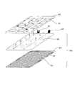
- FIG. 1 is a schematic cross-sectional view of a switch module according to an embodiment of the present invention.
- the top view of the switch module concerning the embodiment of the present invention.
- the schematic perspective view of the conventional switch module The schematic sectional drawing of the conventional switch module.
- FIG. 1A is a schematic cross-sectional view of the switch module 1 according to the present embodiment.
- the switch module 1 is disposed to face a key substrate 8 having a key portion 7, and can be used for, for example, a 10-key substrate and a QWERTY key substrate in an electronic device such as a mobile phone and a notebook PC. is there. It can also be used for a touch panel or the like.
- the switch module 1 includes an LED 2 as a light emitting element, a circuit board 6 having electrodes 11, a metal dome sheet 4 (electrode layer) having a metal dome 5 covering each electrode 11, and The light guide sheet 3 (light guide member) attached by the adhesion layer 10 is provided on the metal dome sheet 4.
- the circuit board 6 an FPC board (FlexibleitPrinted Circuit) can be used.
- a reflector 9 reflecting member that allows light emitted from the LED 2 to enter the light guide sheet 3 efficiently from the end of the LED 2.
- the end of the reflector 9 extends to a position that covers the upper surface of the end of the light sheet 3.
- the key top 7a moves downward in the drawing to press the metal dome sheet 4, thereby deforming the metal dome 5 and bringing the metal dome 5 and the electrode 11 into contact with each other.
- the electrode 11 is electrically connected, that is, the switch is switched from OFF to ON.
- the switch module it is desirable for the switch module to transmit a sufficient click feeling to the user when the key unit is pressed from the viewpoint of operability.
- the switch module has a certain strength. Since the switch is switched between ON and OFF by deformation of the metal dome 5 having the above, a sufficient click feeling can be transmitted to the user.
- Each metal dome 5 is integrally bonded to the metal dome sheet 4, and in the manufacturing process, the metal dome sheet 4 on which the metal dome 5 has been mounted is attached to the circuit board 6, so that the plurality of electrodes 11 are attached.
- the metal dome 5 can be attached with high accuracy and in a simple process.
- the light guide sheet 3 used in this embodiment will be described.
- a urethane rubber sheet (thermosetting) having a thickness of 125 ⁇ m and a Shore hardness of 97 is used, but the material applicable as the light guide sheet 3 is not limited to this,
- a transparent sheet such as a polycarbonate film or a silicone rubber sheet may be used.
- the thickness of the light guide sheet 3 is not particularly limited, it can be said that the thickness is preferably 100 ⁇ m or more and 300 ⁇ m or less.
- the “transparent sheet” here does not necessarily mean colorless and transparent, and the light guide sheet 3 is limited to “colorless and transparent” as long as the light emitted from the LED 2 can be transmitted. is not.
- the switch module 1 can be reduced in size, and the click sensitivity described above can be further improved.
- first surface 3 b the surface facing the key substrate 8
- second surface 3c the surface facing the circuit substrate 6
- the light incident on the light guide sheet 3 is scattered on the second surface 3 c, and the key portion 7 from inside the light guide sheet 3 by the scattered light (light L 2 in FIG. 1B).
- the light scattering processing for illumination which can illuminate is performed.
- dot printing printing processing
- white ink ink having light scattering properties
- ink jet printer whereby white dots 3a are formed on the second surface 3c. It is printed (in this case, white ink is used as the ink having light scattering properties, but ink other than white may be used as long as it has light scattering properties).
- the white dots 3 a are printed at positions corresponding to the key portions 7, whereby the light incident on the light guide sheet 3 from the LEDs 2 is scattered by the white dots 3 a, and the light guide sheet is scattered by the scattered light. It is possible to illuminate the key portion 7 from within 3.
- the dot density, shape, and the like of the white dots 3a are not particularly limited. For example, by increasing the number of white dots 3a in a region away from the LED 2 (region where light is attenuated and transmitted), Even the key portion 7 arranged in a region away from the LED 2 can be illuminated with a sufficient amount of light.
- the form of light scattering processing for illumination is not limited to this, and three-dimensional shape processing by mold processing, laser processing, or the like is performed at a predetermined position to form a concave / convex shape or a prism shape on the light guide sheet 3 It may be a form to do.
- the white dots 3a similarly to the white dots 3a, it is possible to illuminate the key portion 7 suitably by scattering light by the portion subjected to the three-dimensional shape processing.
- the printing process (white dots 3a) is performed on the second surface 3c, but the three-dimensional shape process may be performed on the first surface 3b of the light guide sheet 3.
- the light is scattered in the three-dimensional shape processing applied to the first surface 3b, so that the light is transmitted from the first surface 3b in the direction of the key portion 7, and the key portion 7 is suitably illuminated. It becomes possible.
- emitted from LED2 inject into the light guide sheet 3 efficiently from the edge part of the light guide sheet 3 is provided.
- the thickness of the light guide sheet 3 is often thinner than the light emission area width of the LED 2.
- the reflector 9 is provided at the end of the light guide sheet 3 so as to cover the first surface 3b in order to make light incident more efficiently, but the shape of the reflector 9 is particularly limited. It is not something. Moreover, you may provide a predetermined space
- FIG.1 (b) is the schematic sectional drawing which expanded the vicinity of LED2 about the switch module 1 shown to Fig.1 (a).
- the light emitted from the LED 2 is incident on the light guide sheet 3 from the end of the light guide sheet 3 by the reflector 9 (some light is directly incident on the light guide sheet 3 without going through the reflector 9).
- the first surface 3b and the second surface 3c of the light guide sheet 3 are both in contact with the air layer, and the difference in refractive index (assuming that the refractive index of the air layer is 1.0) Since the refractive index of the sheet 3 is about 1.45), the light traveling in the light guide sheet 3 repeats reflection on the first surface 3b and the second surface 3c as indicated by L1 and L2 in the figure. However, it proceeds toward the other end of the light guide sheet 3.
- the white dot 3a When the white dot 3a is on the optical path, the light is scattered at the white dot 3a, and the light escapes from the light guide sheet 3 in the direction of the key portion 7 as the light indicated by L2.
- the LED 2 After being emitted from the LED 2, there is also light that passes through the adhesive layer 10 and enters the metal dome sheet 4, but this light is also reflected by the surface of the metal dome 5 and transmitted through the adhesive layer 10. The light enters the light guide sheet 3 again.
- FIG. 1C is an enlarged view of the traveling pattern of the light L3 shown in FIG.
- the second surface 3c on the inner side of the reflector 9 (the LED 2 side with respect to the edge portion of the reflector 9), and the light L3 shown in FIGS. 1 (b) and 1 (c).
- a print pattern 12 (printing process) using white ink was formed as a light scattering process for dimming.
- the light L3 leaking from the edge portion of the reflector 9 can be scattered in the print pattern 12 formed on the second surface 3c, so that the amount of light leaking from the edge portion of the reflector 9 is reduced. (The scattered light is absorbed by the circuit board 6 or emitted to the outside).
- white UV curable ink containing main agent: 70 to 90% by mass of photopolymerization composition, pigment: 10 to 20% by mass of titanium dioxide, other: 1 to 5% by mass of polymerization initiator
- main agent 70 to 90% by mass of photopolymerization composition
- pigment 10 to 20% by mass of titanium dioxide
- light scattering processing for dimming is not limited to printing processing, but three-dimensional shape processing by mold processing, laser processing, etc. is performed at a predetermined position to form uneven shapes and prism shapes on the light guide sheet 3 It may be a form to do.
- the amount of light leaking from the vicinity of the edge portion of the reflector 9 can be reduced by scattering the light by the portion subjected to the three-dimensional shape processing, similarly to the printing pattern 12 using the white ink.
- the printed pattern 12 (or three-dimensional shape processing) as the light scattering processing for dimming is printed on the second surface 3c of the reflector 9, but the light scattering processing is performed on the reflector 9 as well. You may give to the 1st surface 3b. Even in this case, the amount of light leaking from the vicinity of the edge portion of the reflector 9 can be reduced.
- light scattering processing printing processing, three-dimensional shape processing
- light scattering processing for dimming may be performed on either the first surface 3b or the second surface 3c of the light guide sheet 3, It is necessary to be applied to the inside of the reflector 9.
- light scattering processing for light reduction is performed on the outside of the reflector 9, the light originally used for irradiating the key portion 7 is scattered by the light scattering processing portion for light reduction, This makes it difficult to illuminate the key unit 7 with a sufficient amount of light.
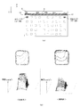
- FIG. 2 is a top view of the switch module 1 according to the present embodiment, and in particular, a diagram schematically showing a position where the print pattern 12 is formed.
- the position where the print pattern 12 made of white ink is formed is not particularly limited as long as it is inside the reflector 9 and on the optical path of light leaking from the vicinity of the edge portion of the reflector 9.
- the print pattern 12 may be formed at the positions shown in FIGS. 2 (a) to 2 (c).
- the “illumination area” in FIGS. 2 (a) to 2 (c) indicates an area corresponding to the key portion 7, but the relative positional relationship between the “illumination area” and the LED 2 is taken into consideration. Thus, it is more effective to determine the position where the print pattern 12 is formed. For example, as shown in FIG. 2A, when the print pattern 12 is formed so that a slit is formed in front of the LED 2, the “illumination area” is prevented from being excessively illuminated, and the LED 2 moves downward (Y direction) from the LED 2. Since more light can be transmitted, even the key portion 7 located away from the LED 2 can be illuminated with a sufficient amount of light. Further, as shown in FIG.
- the print pattern 12 is formed without providing a slit in front of the LED 2, it is possible to more surely prevent the “lighting area” from being excessively illuminated.
- FIG. 2C when there is an “illumination area” in front of the LED 2, if the print pattern 12 is formed in front of the LED 2, it is possible to suitably suppress excessive light in the “illumination area”. it can. That is, the position of the print pattern 12 on the second surface 3c may be any position as long as the light leaking from the “illumination area” can be scattered.
- the print pattern 12 is formed in a rectangular shape.
- the depth (Y direction in FIG. 2) is 0.2 mm to 1.0 mm and the width (X direction in FIG. 2) is 2.0 mm to 5.0 mm
- the key portion It has been found that only light leaking from the edge of the reflector 9 can be effectively scattered without interfering with the optical path of other light that illuminates 7. Further, it has been found that if the printed pattern 12 is 0.3 mm or more inside from the edge portion of the reflector 9, light can be scattered more effectively without interfering with other light.
- the shape of the print pattern 12 is not particularly limited, and may be an ellipse, a circle, a set of dots, or the like.
- the dimensions may be any dimensions that can effectively scatter only the light leaking from the edge portion of the reflector 9 in view of the radiation angle of the LED 2 and the position of the “illumination area”.
- FIG. 3A is a schematic diagram showing an arrangement of the “illumination area” (area corresponding to the key portion) and the LED 2 used in the verification experiment
- FIG. 3B is a diagram (Comparative Example (left)) and FIG. It is the brightness
- the “illumination areas” in the upper left and upper right were targeted, and the luminance was compared between (Comparative Example) and (Example).
- the luminance of the “illuminated area” in the upper left is 39.6 cd / m 2
- the luminance of the “illuminated area” in the upper right is 37.2 cd / m 2 . It was found that the brightness is higher than the brightness. However, locally, the upper left area near the LED 2 in the upper left “illumination area”, and the upper right area near the LED 2 in the upper right “illumination area”. , Each of which has been confirmed to be extremely bright.
- a white ink print pattern 12 is formed, the depth (Y direction in the figure) dimension of the print pattern 12 is 0.5 mm, and the width (X direction in the figure) dimension is 4. 0.0 mm.
- a result of measuring the brightness at such a condition (39.6cd / m 2 in the comparative example) luminance 26.2cd / m 2 of the "illuminated area" in the upper left, the luminance of the "illuminated area” in the upper right 25.1cd / m 2 (37.2 cd / m 2 in the comparative example) was confirmed to be significantly reduced. Further, in the other “illuminated areas”, almost no decrease in luminance was observed. In other words, it was found that “excessive light” can be suppressed and the requirement of “luminance uniformity” can be satisfied.
- FIG. 3B shows a luminance contour map of the “illumination area” in the upper left of FIG. 3A in (Comparative Example) and (Example).
- the upper side shows a luminance contour map when the upper left “illumination area” is viewed from above, and the lower side shows a three-dimensional luminance contour map of the upper left “illumination area”. It is.
- the entire “illumination area” has high luminance, and in particular, the upper left region near the LED 2 shows extremely high luminance.
- luminance has fallen as a whole. That is, it can be seen that “too much light” can be reliably suppressed by forming the print pattern 12 of the white ink.
- the switch module 1 which concerns on this embodiment, the light quantity which leaks from the edge part vicinity of the reflector 9 can be reduced by the above-mentioned structure. Therefore, in the conventional configuration, when the key part is arranged close to the LED, there is a problem that the key part in the vicinity of the LED is excessively lit due to the leaked light, and thereby the key part is arranged close to the LED. However, in the present embodiment, even if the key portion 7 is arranged close to the LED 2, such an excessive light problem does not occur. Therefore, the distance a shown in FIG. 1B (the distance between the key portion 7 closest to the LED 2 and the LED 2) can be reduced, that is, the key portion 7 can be arranged close to the LED 2, and the arrangement of the key portion can be reduced. Design restrictions can be relaxed.
- the present embodiment it is possible to suppress a phenomenon in which the key portion 7 disposed in the vicinity of the LED 2 is excessively bright as compared with the other key portions 7. Further, the white ink print pattern 12 formed on the second surface 3c is formed only on the optical path of the light leaking from the edge portion of the reflector 9, so that the key portion 7 is illuminated. Other light (for example, L1 and L2 in FIG. 1B) is not affected at all, and even the key portion 7 separated from the LED 2 can be illuminated with a sufficient amount of light. Therefore, it is possible to illuminate the plurality of key portions 7 arranged on the key substrate 8 with substantially uniform luminance, and it is possible to satisfy the requirement of “luminance uniformity”.
- a white ink print pattern 12 is printed on the second surface 3c of the light guide sheet 3 as light scattering processing for dimming, and white dots 3a are printed on the second surface 3c as light scattering processing for illumination.
- the white dots 3a and the print pattern 12 made of white ink are printed by inkjet on the same surface (second surface 3c) of the light guide sheet 3, the same manufacturing equipment (printing) is used in the manufacturing process. Device), the white dots 3a and the white ink print pattern 12 can be printed on the same surface with high positional accuracy in the same process, leading to improved production efficiency and reduced manufacturing costs (same ink). Can also be used).
- the same effect is obtained because the three-dimensional shape processing is performed on the same surface. Can do.
- the switch module provided facing the key substrate the amount of light leaking from the vicinity of the edge portion of the reflector toward the key portion is reduced, and the light traveling in the light guide member is used. It is possible to provide a switch module that can uniformly illuminate the key portion.
Landscapes
- Push-Button Switches (AREA)
Abstract
Description
特許文献2:特開2008-152951号公報
特許文献3:特開2009-140871号公報
特許文献4:特開2009-187855号公報
特許文献5:特開2004-139983号公報
特許文献6:特開2008-226844号公報
キー部を有するキー基板に対向して設けられるスイッチモジュールであって、
前記キー基板に対向する表面に電極層が形成された回路基板と、
前記キー基板と前記回路基板との間に設けられている導光部材と、
光を射出する光源素子と、
前記光源素子から射出された光を前記導光部材の端部から前記導光部材内に入射させる反射部材と、
を備え、
前記電極層に対して前記キー部が移動することで、スイッチのON、OFFが切り換えられると共に、前記導光部材内に入射した光によって前記導光部材内から前記キー部を照明可能であるスイッチモジュールにおいて、
前記導光部材は、前記キー基板と対向する第1の面と、その反対側にあって前記回路基板と対向する第2の面とを有し、前記反射部材が前記端部における第1の面を覆うようにして設けられていると共に、
前記導光部材において前記反射部材の内側には、
前記反射部材によって前記導光部材内に入射された光であって、前記反射部材のエッジ部近傍から第1の面を透過する光の光路上に、前記エッジ部近傍から第1の面を透過する光の光量を低減させるための減光用の光散乱加工が施されていることを特徴とする。
前記導光部材には、
前記導光部材内に入射した光を散乱させ、散乱した光によって前記導光部材内から前記キー部を照明可能な照明用の光散乱加工が施されていると好適である。
前記減光用の光散乱加工、及び前記照明用の光散乱加工とは、
光散乱性を有するインクを前記導光部材に印刷する印刷加工、又は、
光散乱性を有する3次元形状を前記導光部材に形成する3次元形状加工、
であると好適である。
前記減光用の光散乱加工、及び前記照明用の光散乱加工が、
共に前記導光部材の第2の面に施されていると好適である。
前記導光部材には、
厚さが100μm以上300μm以下の光透過性を有するシート部材が用いられていると好適である。
<1:スイッチモジュールの全体構成について>
図1(a)を参照して、本発明を適用可能な実施形態に係るスイッチモジュール1の全体構成について説明する。図1(a)は、本実施形態に係るスイッチモジュール1の概略断面図である。
本実施形態に用いられている導光シート3について説明する。本実施形態では、厚さ125μm、ショア硬度97の光透過性を有するウレタンゴムシート(熱硬化性)を用いているが、導光シート3として適用可能な材料はこれに限られるものではなく、ポリカーボネートフィルム、シリコンゴムシート等の透明シートを用いてもよい。また、導光シート3の厚さは特に限定されるものではないが、厚さ100μm以上300μm以下であるとより好適であるといえる。なお、ここでいう「透明シート」とは、必ずしも無色透明を意味するものではなく、LED2から射出された光が透過可能なものであれば、導光シート3は「無色透明」に限られるものではない。
本実施形態では、LED2から射出された光を導光シート3の端部から導光シート3内に効率的に入射させるためのリフレクター9が設けられている。本実施形態のように厚さの薄い導光シート3を用いる場合は、LED2の光射出領域幅よりも導光シート3の厚さの方が薄くなっていることが多く、このような場合は、LED2から射出された光を効率的に導光シート3内に入射させるためにも、LED2と導光シート3との間にリフレクター9を設けることが有効である。本実施形態では、より効率的に光を入射させるべく、導光シート3の端部において、リフレクター9が第1の面3bを覆うように設けられているが、リフレクター9の形状は特に限定されるものではない。また、リフレクター9と第1の面3bとの間に所定の間隔を設けてもよいし、間隔を設けずにリフレクター9と第1の面3bとを密着させてもよい。
図1(b)を参照して、本実施形態における導光シート3内の光の進み方について説明する。図1(b)は、図1(a)に示すスイッチモジュール1について、LED2の近傍を拡大した概略断面図である。
図1(b)、図1(c)を参照して、従来の課題として挙げられている「光の漏れ」を低減する構成について説明する。図1(c)は、図1(b)に示す光L3の進行パターンを拡大した図である。
図2を参照して、印刷パターン12の位置、形状について説明する。図2は、本実施形態に係るスイッチモジュール1の上面図であり、特に、印刷パターン12が形成される位置を模式的に示している図である。
(比較例)と(実施例)のそれぞれに対して、「照光エリア」の光り過ぎを抑制する効果を検証する検証実験を行った。以下、図3(a)、図3(b)を参照して、検証実験の条件、結果について説明する。図3(a)は、検証実験に用いた「照光エリア」(キー部に対応するエリア)、LED2の配置を示す模式図であり、図3(b)は、(比較例(左))と(実施例(右))のそれぞれで測定した輝度等高線図である(上側は上面から見た図、下側は3次元状に表した図)。なお、輝度測定用装置には、HI-LAND社製 RISA-COLOR/ONEIIを用いた。
比較例として、図3(a)に示す「照光エリア」(キー部)の配置において、白色インクの印刷パターン12を形成しない場合について、「照光エリア」の輝度(cd/m2)を測定した。発明者らの鋭意検討によれば、図示する複数の「照光エリア」のうち、左上と右上にある「照光エリア」(斜線部で示すエリア)に顕著な「光り過ぎ」の現象が生じており、これにより、満足のいくレベルの「輝度均一性」が達成できていないことが確認されている。そこで、左上と右上にある「照光エリア」を対象とし、(比較例)と(実施例)とでその輝度を比較した。なお、(比較例)では、左上の「照光エリア」の輝度が39.6cd/m2で、右上の「照光エリア」の輝度が37.2cd/m2であり、他の「照光エリア」の輝度と比較すると高い輝度を示すことがわかったが、さらに、局所的には、左上の「照光エリア」では、LED2に近い左上領域が、右上の「照光エリア」では、LED2に近い右上領域が、それぞれ極端に光り過ぎていることが確認されている。
実施例では、図3(a)に示すように白色インクの印刷パターン12を形成し、印刷パターン12の奥行き(図中Y方向)寸法を0.5mm、幅(図中X方向)寸法を4.0mmとした。かかる条件で輝度を測定した結果、左上の「照光エリア」の輝度が26.2cd/m2(比較例では39.6cd/m2)、右上の「照光エリア」の輝度が25.1cd/m2(比較例では37.2cd/m2)にそれぞれ大幅に低下していることが確認された。また、他の「照光エリア」では、輝度の低下がほとんど見られなかった。すなわち「光り過ぎ」を抑制し、「輝度均一性」の要求を満たせることがわかった。
本実施形態に係るスイッチモジュール1によれば、従来の構成では得ることができなかった以下の効果を得ることが可能になる。
本実施形態に係るスイッチモジュール1によれば、上述の構成によって、リフレクター9のエッジ部近傍から漏れ出る光の光量を低減することができる。よって、従来の構成ではキー部をLEDに近づけて配置すると、漏れ出た光によってLED近傍にあるキー部が極端に光り過ぎるといった課題が生じ、これにより、キー部をLEDに近づけて配置することが出来ないといった、設計上、デザイン上の制約が生じていたが、本実施形態では、キー部7をLED2に近づけて配置しても、このような光り過ぎの課題を生じることはない。よって、図1(b)で示す距離a(LED2に最も近いキー部7とLED2との間隔)を狭くすること、即ち、キー部7をLED2に近づけて配置することができ、キー部配置の設計上、デザイン上の制約を緩和することができる。
本実施形態によれば、LED2近傍に配置されたキー部7が他のキー部7と比較して極端に光り過ぎるといった現象を抑制できる。また、第2の面3c上に形成される白色インクの印刷パターン12は、リフレクター9のエッジ部から漏れ出る光の光路上にのみ形成されるものであるので、キー部7を照明するための他の光(例えば図1(b)のL1、L2)には何ら影響はなく、LED2から離れたキー部7であっても十分な光量で照明することができる。よって、キー基板8に配置されている複数のキー部7をほぼ均一な輝度で照明することができ、「輝度均一性」の要求を満たすことが可能になる。
導光シート3の第2の面3cに、減光用の光散乱加工として白色インクの印刷パターン12を印刷し、さらに第2の面3cに照明用の光散乱加工として白色ドット3aを印刷する場合は、導光シート3の同一面(第2の面3c)に白色ドット3a、及び白色インクによる印刷パターン12がインクジェットによって印刷されることになるので、製造過程では、同一の製造機器(印刷機器)を使用して、同一面に白色ドット3aと白色インクの印刷パターン12とを同一工程内で位置精度よく印刷することができ、生産効率の向上、製造コストの低減につながる(同一のインクの使用することも可能である)。また、減光用の光散乱加工、及び照明用の光散乱加工として、共に3次元形状加工を選択する場合も、同一面に3次元形状加工を施すことになるので、同様の効果を得ることができる。
Claims (5)
- キー部を有するキー基板に対向して設けられるスイッチモジュールであって、
前記キー基板に対向する表面に電極層が形成された回路基板と、
前記キー基板と前記回路基板との間に設けられている導光部材と、
光を射出する光源素子と、
前記光源素子から射出された光を前記導光部材の端部から前記導光部材内に入射させる反射部材と、
を備え、
前記電極層に対して前記キー部が移動することで、スイッチのON、OFFが切り換えられると共に、前記導光部材内に入射した光によって前記導光部材内から前記キー部を照明可能であるスイッチモジュールにおいて、
前記導光部材は、前記キー基板と対向する第1の面と、その反対側にあって前記回路基板と対向する第2の面とを有し、前記反射部材が前記端部における第1の面を覆うようにして設けられていると共に、
前記導光部材において前記反射部材の内側には、
前記反射部材によって前記導光部材内に入射された光であって、前記反射部材のエッジ部近傍から第1の面を透過する光の光路上に、前記エッジ部近傍から第1の面を透過する光の光量を低減させるための減光用の光散乱加工が施されていることを特徴とするスイッチモジュール。 - 前記導光部材には、
前記導光部材内に入射した光を散乱させ、散乱した光によって前記導光部材内から前記キー部を照明可能な照明用の光散乱加工が施されていることを特徴とする請求項1に記載のスイッチモジュール。 - 前記減光用の光散乱加工、及び前記照明用の光散乱加工とは、
光散乱性を有するインクを前記導光部材に印刷する印刷加工、又は、
光散乱性を有する3次元形状を前記導光部材に形成する3次元形状加工、
であることを特徴とする請求項2に記載のスイッチモジュール。 - 前記減光用の光散乱加工、及び前記照明用の光散乱加工が、
共に前記導光部材の第2の面に施されていることを特徴とする請求項2また3に記載のスイッチモジュール。 - 前記導光部材には、
厚さが100μm以上300μm以下の光透過性を有するシート部材が用いられていることを特徴とする請求項1乃至4のいずれか1項に記載のスイッチモジュール。
Priority Applications (4)
| Application Number | Priority Date | Filing Date | Title |
|---|---|---|---|
| HK13100978.1A HK1174145B (en) | 2010-02-17 | 2010-10-28 | Switch module |
| CN201080061276.0A CN102714104B (zh) | 2010-02-17 | 2010-10-28 | 开关模块 |
| US13/500,981 US8742273B2 (en) | 2010-02-17 | 2010-10-28 | Switch module |
| EP10846152.6A EP2538426A4 (en) | 2010-02-17 | 2010-10-28 | SWITCHING MODULE |
Applications Claiming Priority (2)
| Application Number | Priority Date | Filing Date | Title |
|---|---|---|---|
| JP2010032568A JP5427637B2 (ja) | 2010-02-17 | 2010-02-17 | スイッチモジュール |
| JP2010-032568 | 2010-02-17 |
Publications (1)
| Publication Number | Publication Date |
|---|---|
| WO2011102020A1 true WO2011102020A1 (ja) | 2011-08-25 |
Family
ID=44482633
Family Applications (1)
| Application Number | Title | Priority Date | Filing Date |
|---|---|---|---|
| PCT/JP2010/069149 Ceased WO2011102020A1 (ja) | 2010-02-17 | 2010-10-28 | スイッチモジュール |
Country Status (6)
| Country | Link |
|---|---|
| US (1) | US8742273B2 (ja) |
| EP (1) | EP2538426A4 (ja) |
| JP (1) | JP5427637B2 (ja) |
| CN (1) | CN102714104B (ja) |
| TW (1) | TWI489501B (ja) |
| WO (1) | WO2011102020A1 (ja) |
Families Citing this family (3)
| Publication number | Priority date | Publication date | Assignee | Title |
|---|---|---|---|---|
| TR201712255A2 (tr) * | 2017-08-17 | 2017-09-21 | Eae Teknoloji Arastirma Gelistirme Sanayi Ve Ticaret Anonim Sirketi | Gi̇zli̇ yüzey aydinlatma terti̇bati |
| CN113539714A (zh) * | 2020-04-14 | 2021-10-22 | 褚锦雄 | 带led灯的按压开关 |
| TWI885859B (zh) * | 2023-11-28 | 2025-06-01 | 達方電子股份有限公司 | 發光按鍵 |
Citations (11)
| Publication number | Priority date | Publication date | Assignee | Title |
|---|---|---|---|---|
| JP2004139983A (ja) | 2002-09-27 | 2004-05-13 | Shin Etsu Polymer Co Ltd | 押釦スイッチ用カバー部材 |
| JP2007087749A (ja) * | 2005-09-21 | 2007-04-05 | Citizen Electronics Co Ltd | シートスイッチ、シートスイッチモジュール及びパネルスイッチ |
| JP2008152951A (ja) | 2006-12-14 | 2008-07-03 | Citizen Electronics Co Ltd | シートスイッチモジュール |
| JP2008159541A (ja) * | 2006-12-26 | 2008-07-10 | Alps Electric Co Ltd | スイッチ用照光部材およびそれを用いたスイッチ装置 |
| JP2008226844A (ja) | 2007-03-14 | 2008-09-25 | Samsung Electronics Co Ltd | 導波部材及びそれを用いるキーパッドアセンブリ |
| JP2009094036A (ja) * | 2007-10-12 | 2009-04-30 | Panasonic Corp | 可動接点体及びこれを用いたスイッチ |
| JP2009140871A (ja) | 2007-12-10 | 2009-06-25 | Alps Electric Co Ltd | スイッチ用照光部材、及びスイッチ用照光部材を有するスイッチ装置 |
| JP2009187855A (ja) | 2008-02-08 | 2009-08-20 | Shin Etsu Polymer Co Ltd | 携帯電話の照明構造 |
| JP2009246821A (ja) | 2008-03-31 | 2009-10-22 | Fujitsu Ltd | 携帯端末装置 |
| JP2010015794A (ja) * | 2008-07-03 | 2010-01-21 | Citizen Electronics Co Ltd | 導光シートスイッチユニット |
| JP2010034008A (ja) * | 2008-07-31 | 2010-02-12 | Citizen Electronics Co Ltd | 導光シートスイッチユニット |
Family Cites Families (12)
| Publication number | Priority date | Publication date | Assignee | Title |
|---|---|---|---|---|
| US5771321A (en) * | 1996-01-04 | 1998-06-23 | Massachusetts Institute Of Technology | Micromechanical optical switch and flat panel display |
| JP2001291414A (ja) * | 2000-04-10 | 2001-10-19 | Advanced Display Inc | 面状光源装置およびこれを備えた液晶表示装置 |
| TW200709243A (en) | 2005-08-19 | 2007-03-01 | Citizen Electronics | Sheet switch, sheet switch module and panel switch |
| JP4728067B2 (ja) * | 2005-08-19 | 2011-07-20 | シチズン電子株式会社 | シートスイッチモジュール |
| US7683279B2 (en) * | 2006-02-28 | 2010-03-23 | Hyun Soo Kim | Light emitting keypad comprising light guide film and light guide |
| US7736042B2 (en) * | 2006-07-20 | 2010-06-15 | Ls Tech Co., Ltd. | Back light unit |
| CN101583822A (zh) * | 2007-01-15 | 2009-11-18 | 阿尔卑斯电气株式会社 | 照明装置以及具备该照明装置的输入装置 |
| US20080175022A1 (en) * | 2007-01-22 | 2008-07-24 | Takuro Sugiura | Illuminating unit |
| US7718910B2 (en) * | 2007-06-20 | 2010-05-18 | Panasonic Corporation | Movable contact assembly and switch using the same |
| JP5136934B2 (ja) * | 2008-04-07 | 2013-02-06 | 住友電工プリントサーキット株式会社 | フレキシブルプリント配線板、入力モジュール及び携帯機器 |
| WO2009157218A1 (ja) * | 2008-06-26 | 2009-12-30 | 日本メクトロン株式会社 | 携帯機器のキーモジュール |
| TWI430310B (zh) * | 2010-12-20 | 2014-03-11 | Primax Electronics Ltd | 發光鍵盤 |
-
2010
- 2010-02-17 JP JP2010032568A patent/JP5427637B2/ja not_active Expired - Fee Related
- 2010-10-28 WO PCT/JP2010/069149 patent/WO2011102020A1/ja not_active Ceased
- 2010-10-28 EP EP10846152.6A patent/EP2538426A4/en not_active Withdrawn
- 2010-10-28 US US13/500,981 patent/US8742273B2/en not_active Expired - Fee Related
- 2010-10-28 CN CN201080061276.0A patent/CN102714104B/zh not_active Expired - Fee Related
-
2011
- 2011-02-16 TW TW100105068A patent/TWI489501B/zh not_active IP Right Cessation
Patent Citations (11)
| Publication number | Priority date | Publication date | Assignee | Title |
|---|---|---|---|---|
| JP2004139983A (ja) | 2002-09-27 | 2004-05-13 | Shin Etsu Polymer Co Ltd | 押釦スイッチ用カバー部材 |
| JP2007087749A (ja) * | 2005-09-21 | 2007-04-05 | Citizen Electronics Co Ltd | シートスイッチ、シートスイッチモジュール及びパネルスイッチ |
| JP2008152951A (ja) | 2006-12-14 | 2008-07-03 | Citizen Electronics Co Ltd | シートスイッチモジュール |
| JP2008159541A (ja) * | 2006-12-26 | 2008-07-10 | Alps Electric Co Ltd | スイッチ用照光部材およびそれを用いたスイッチ装置 |
| JP2008226844A (ja) | 2007-03-14 | 2008-09-25 | Samsung Electronics Co Ltd | 導波部材及びそれを用いるキーパッドアセンブリ |
| JP2009094036A (ja) * | 2007-10-12 | 2009-04-30 | Panasonic Corp | 可動接点体及びこれを用いたスイッチ |
| JP2009140871A (ja) | 2007-12-10 | 2009-06-25 | Alps Electric Co Ltd | スイッチ用照光部材、及びスイッチ用照光部材を有するスイッチ装置 |
| JP2009187855A (ja) | 2008-02-08 | 2009-08-20 | Shin Etsu Polymer Co Ltd | 携帯電話の照明構造 |
| JP2009246821A (ja) | 2008-03-31 | 2009-10-22 | Fujitsu Ltd | 携帯端末装置 |
| JP2010015794A (ja) * | 2008-07-03 | 2010-01-21 | Citizen Electronics Co Ltd | 導光シートスイッチユニット |
| JP2010034008A (ja) * | 2008-07-31 | 2010-02-12 | Citizen Electronics Co Ltd | 導光シートスイッチユニット |
Non-Patent Citations (1)
| Title |
|---|
| See also references of EP2538426A4 |
Also Published As
| Publication number | Publication date |
|---|---|
| US20120193200A1 (en) | 2012-08-02 |
| JP2011171059A (ja) | 2011-09-01 |
| HK1174145A1 (en) | 2013-05-31 |
| EP2538426A1 (en) | 2012-12-26 |
| CN102714104A (zh) | 2012-10-03 |
| CN102714104B (zh) | 2015-06-10 |
| EP2538426A4 (en) | 2015-11-18 |
| US8742273B2 (en) | 2014-06-03 |
| TW201205627A (en) | 2012-02-01 |
| JP5427637B2 (ja) | 2014-02-26 |
| TWI489501B (zh) | 2015-06-21 |
Similar Documents
| Publication | Publication Date | Title |
|---|---|---|
| CN101266317B (zh) | 波导部件和使用该波导部件的键盘组件 | |
| JP5427638B2 (ja) | スイッチモジュール | |
| TWI542910B (zh) | 光導元件及其製造方法以及顯示元件 | |
| US20100097246A1 (en) | Input device and keyboard device having illumination function | |
| JP2007234584A (ja) | タッチセンサー装置 | |
| JP2012018917A (ja) | 面状発光装置およびシートスイッチモジュール | |
| CN105299542B (zh) | 背光模组 | |
| JP4829811B2 (ja) | 照光ユニット | |
| JP5427637B2 (ja) | スイッチモジュール | |
| JP5427639B2 (ja) | スイッチモジュール | |
| JP2013143274A (ja) | 面状発光装置およびシートスイッチモジュール | |
| JP5486952B2 (ja) | スイッチモジュール | |
| KR101086670B1 (ko) | 백라이트 유닛의 도광판 및 그 제조방법 | |
| CN114914114B (zh) | 发光键盘及其光学模块 | |
| HK1174145B (en) | Switch module | |
| HK1174146B (en) | Switch module | |
| JP2015153376A (ja) | 操作検出装置 | |
| JP2009283142A (ja) | 導光板、配線モジュールおよび電子機器 |
Legal Events
| Date | Code | Title | Description |
|---|---|---|---|
| WWE | Wipo information: entry into national phase |
Ref document number: 201080061276.0 Country of ref document: CN |
|
| 121 | Ep: the epo has been informed by wipo that ep was designated in this application |
Ref document number: 10846152 Country of ref document: EP Kind code of ref document: A1 |
|
| REEP | Request for entry into the european phase |
Ref document number: 2010846152 Country of ref document: EP |
|
| WWE | Wipo information: entry into national phase |
Ref document number: 2010846152 Country of ref document: EP |
|
| WWE | Wipo information: entry into national phase |
Ref document number: 13500981 Country of ref document: US |
|
| NENP | Non-entry into the national phase |
Ref country code: DE |