WO2011105438A1 - 距離画像センサ - Google Patents
距離画像センサ Download PDFInfo
- Publication number
- WO2011105438A1 WO2011105438A1 PCT/JP2011/054006 JP2011054006W WO2011105438A1 WO 2011105438 A1 WO2011105438 A1 WO 2011105438A1 JP 2011054006 W JP2011054006 W JP 2011054006W WO 2011105438 A1 WO2011105438 A1 WO 2011105438A1
- Authority
- WO
- WIPO (PCT)
- Prior art keywords
- modulation signal
- transfer electrode
- period
- image sensor
- distance image
- Prior art date
- Legal status (The legal status is an assumption and is not a legal conclusion. Google has not performed a legal analysis and makes no representation as to the accuracy of the status listed.)
- Ceased
Links
Images







Classifications
-
- G—PHYSICS
- G01—MEASURING; TESTING
- G01S—RADIO DIRECTION-FINDING; RADIO NAVIGATION; DETERMINING DISTANCE OR VELOCITY BY USE OF RADIO WAVES; LOCATING OR PRESENCE-DETECTING BY USE OF THE REFLECTION OR RERADIATION OF RADIO WAVES; ANALOGOUS ARRANGEMENTS USING OTHER WAVES
- G01S17/00—Systems using the reflection or reradiation of electromagnetic waves other than radio waves, e.g. lidar systems
- G01S17/88—Lidar systems specially adapted for specific applications
- G01S17/89—Lidar systems specially adapted for specific applications for mapping or imaging
-
- G—PHYSICS
- G01—MEASURING; TESTING
- G01S—RADIO DIRECTION-FINDING; RADIO NAVIGATION; DETERMINING DISTANCE OR VELOCITY BY USE OF RADIO WAVES; LOCATING OR PRESENCE-DETECTING BY USE OF THE REFLECTION OR RERADIATION OF RADIO WAVES; ANALOGOUS ARRANGEMENTS USING OTHER WAVES
- G01S7/00—Details of systems according to groups G01S13/00, G01S15/00, G01S17/00
- G01S7/48—Details of systems according to groups G01S13/00, G01S15/00, G01S17/00 of systems according to group G01S17/00
- G01S7/483—Details of pulse systems
- G01S7/486—Receivers
- G01S7/4861—Circuits for detection, sampling, integration or read-out
- G01S7/4863—Detector arrays, e.g. charge-transfer gates
-
- G—PHYSICS
- G01—MEASURING; TESTING
- G01J—MEASUREMENT OF INTENSITY, VELOCITY, SPECTRAL CONTENT, POLARISATION, PHASE OR PULSE CHARACTERISTICS OF INFRARED, VISIBLE OR ULTRAVIOLET LIGHT; COLORIMETRY; RADIATION PYROMETRY
- G01J1/00—Photometry, e.g. photographic exposure meter
- G01J1/42—Photometry, e.g. photographic exposure meter using electric radiation detectors
- G01J1/44—Electric circuits
- G01J1/46—Electric circuits using a capacitor
-
- G—PHYSICS
- G01—MEASURING; TESTING
- G01S—RADIO DIRECTION-FINDING; RADIO NAVIGATION; DETERMINING DISTANCE OR VELOCITY BY USE OF RADIO WAVES; LOCATING OR PRESENCE-DETECTING BY USE OF THE REFLECTION OR RERADIATION OF RADIO WAVES; ANALOGOUS ARRANGEMENTS USING OTHER WAVES
- G01S17/00—Systems using the reflection or reradiation of electromagnetic waves other than radio waves, e.g. lidar systems
- G01S17/88—Lidar systems specially adapted for specific applications
- G01S17/89—Lidar systems specially adapted for specific applications for mapping or imaging
- G01S17/894—Three-dimensional [3D] imaging with simultaneous measurement of time-of-flight at a two-dimensional [2D] array of receiver pixels, e.g. time-of-flight cameras or flash lidar
-
- G—PHYSICS
- G01—MEASURING; TESTING
- G01S—RADIO DIRECTION-FINDING; RADIO NAVIGATION; DETERMINING DISTANCE OR VELOCITY BY USE OF RADIO WAVES; LOCATING OR PRESENCE-DETECTING BY USE OF THE REFLECTION OR RERADIATION OF RADIO WAVES; ANALOGOUS ARRANGEMENTS USING OTHER WAVES
- G01S7/00—Details of systems according to groups G01S13/00, G01S15/00, G01S17/00
- G01S7/48—Details of systems according to groups G01S13/00, G01S15/00, G01S17/00 of systems according to group G01S17/00
- G01S7/483—Details of pulse systems
- G01S7/486—Receivers
- G01S7/487—Extracting wanted echo signals, e.g. pulse detection
- G01S7/4876—Extracting wanted echo signals, e.g. pulse detection by removing unwanted signals
-
- H—ELECTRICITY
- H01—ELECTRIC ELEMENTS
- H01J—ELECTRIC DISCHARGE TUBES OR DISCHARGE LAMPS
- H01J1/00—Details of electrodes, of magnetic control means, of screens, or of the mounting or spacing thereof, common to two or more basic types of discharge tubes or lamps
- H01J1/46—Control electrodes, e.g. grid; Auxiliary electrodes
Definitions
- the present invention relates to a distance image sensor.
- an image sensor that can obtain a distance image of an object is expected. It is also expected to obtain the actual image of the measurement object and the distance image with the same chip.
- a distance image sensor is expected to be applied to various technologies. For example, if a distance image sensor is mounted on a moving body such as a ship, an automobile, or an aircraft, a distance image of an object around the moving body can be obtained. Therefore, based on the obtained distance image of the object, the moving object Can be controlled. In factory automation (FA), when a distance image of an object is obtained, the object can be inspected / controlled using the distance image.
- FA factory automation
- TOF-Flight Time-OF-Flight
- this method requires a light source (such as a pulse laser or a light emitting diode (LED)) and a light receiving element.
- the distance image sensor using the charge distribution structure the distance is calculated based on the ratio between the accumulated charges distributed at a certain period and the accumulated charges different from the phase. That is, the phase shift of the reflected return light with respect to the phase of the emitted light is regarded as the distance to the object, and the charge generated in response to the return light is distributed in synchronization with the modulation period of the emitted light, and the phase shift The amount is calculated using the ratio of the distributed charge amount.
- Patent Document 1 electric charges are distributed by two light receiving units and two storage capacitors.
- a plurality of pixels are two-dimensionally arranged, and distance information to an object obtained in each pixel is two-dimensionally output.
- at least two capacitors are provided in one pixel, and charges derived from background light are canceled using these two capacitors.
- one capacitor is provided in one pixel, and a distributed signal is supplied to each electrode terminal of the capacitor at different times via only a pair of switches. Is integrated to control the electric charge flowing into the capacitor and cancel the current derived from the background light.
- the distance image sensor described in Patent Document 1 has a large number of capacitors, so the size of one pixel is increased, and the spatial resolution is improved. Can not do it.
- circuit elements such as capacitors and switches
- parasitic capacitance increases and output linearity decreases.
- the time correlation detection type image sensor described in Patent Document 2 although the spatial resolution is increased by reducing the number of capacitors, switching noise is superimposed on the signal due to an increase in the number of switching circuits. Cannot be calculated. Therefore, any of the conventional techniques has a problem that an accurate distance image cannot be obtained.
- the present invention has been made in view of such a problem, and an object thereof is to provide a distance image sensor capable of obtaining an accurate distance image.
- a distance image sensor is a distance image including an imaging region that receives reflected light of light emitted to an object and a drive circuit that drives the imaging region.
- the imaging region includes a plurality of pixels arranged one-dimensionally or two-dimensionally on a semiconductor substrate, and each pixel includes a light-receiving region and first and second adjacent to the light-receiving region. Electrically connected between the first and second storage regions, and the first and second transfer electrodes for controlling the flow of charge into the first and second storage regions, respectively.
- the circuit sets a reset period in which all of the first, second, third, and fourth switches are turned on at the first time of one cycle, and the first period and the second period alternate in one cycle. In the first period, both the first and third switches are turned on, both the second and fourth switches are turned off, and in the second period, the first and third switches are turned on.
- Both the second switch and the fourth switch are turned OFF, and both the second and fourth switches are turned ON, and the first and second transfer electrodes are synchronized with the modulation signal of the emitted light within the one period, and have opposite phases to each other.
- the modulation signal is provided.
- Noise based on the light quantum (photon shot noise) increases at the square root of the exposure light quantity, and the signal component increases proportionally. Therefore, as the exposure time is increased, the ratio of the signal component increases, and the signal to noise ratio increases. Will improve. Therefore, as the charges distributed in the first and second storage regions are integrated by the first and second transfer electrodes, the signal-to-noise ratio is improved and an accurate distance image can be obtained. That is, by applying a modulation signal to the transfer electrode, charge integration for a certain period is performed in the first and second accumulation regions, and simultaneously or after integration, the charge integrated in the first accumulation region is changed to the first accumulation region. In the first period, the charge connected to the first terminal of the capacitor and integrated in the second accumulation region is connected to the second terminal of the capacitor in the second period. The charge component contained, that is, the background light component is canceled out.
- each storage region is connected to only a single capacitor, the pixel size can be reduced to improve the spatial resolution.
- the first and second storage regions are also provided. Since the charge transferred into the capacitor is integrated, the signal-to-noise ratio is improved, and the number of times of switching during charge transfer to the capacitor of the first and second switches is reduced, so that the switching noise is also reduced.
- the electric charge corresponding to the distance is accumulated in this, and the accurate distance can be calculated by detecting the amount of electric charge (voltage corresponding to this). Further, in this application, since the photocurrent is integrated as a charge for a predetermined period and then the distribution operation is performed, the noise is less than that in which the photocurrent is directly distributed to the capacitor as in Patent Document 2.
- the drive circuit includes the first or second switch so that the number of switching times of the first and second switches after the end of the reset period within the one cycle is equal.
- the second switch is additionally switched.
- additional switching hereinafter referred to as “dummy switching”
- the drive circuit includes (a) the first circuit at a timing having a phase difference of 0 ° with the modulated signal of the emitted light within a specific period.
- a modulation signal is given to the transfer electrode, a modulation signal having a phase opposite to that of the modulation signal given to the first transfer electrode is given to the second transfer electrode, and (b) the emission light within another period
- the modulation signal is applied to the first transfer electrode at a timing having a phase difference of 90 ° with respect to the modulation signal, and the modulation signal applied to the first transfer electrode is opposite in phase to the second transfer electrode.
- the modulation signal is applied to the first transfer electrode at a timing having a phase difference of 180 ° from the modulation signal of the emitted light, and the second transfer A modulation signal applied to the first transfer electrode.
- a modulation signal to the first transfer electrode at a timing having a phase difference of 270 ° from the modulation signal of the emitted light within another period different from the above.
- a modulation signal having a phase opposite to that of the modulation signal applied to the first transfer electrode is applied to the second transfer electrode, and the first period within one cycle of (a) to (d). And the order of the second period is the same.
- the number of times the charge transferred to the capacitor is switched is different at each terminal of the capacitor.
- the charge is stored in each storage region in the four phases (a) to (d).
- the offset component can be canceled together with the background light component. Thereby, an accurate distance can be calculated.
- the drive circuit includes (a) the first circuit at a timing having a phase difference of 0 ° with the modulation signal of the emitted light within a specific period.
- a modulation signal is given to the transfer electrode, a modulation signal having a phase opposite to that of the modulation signal given to the first transfer electrode is given to the second transfer electrode, and (b) the emission light within another period
- the modulation signal is applied to the first transfer electrode at a timing having a phase difference of 90 ° with respect to the modulation signal, and the modulation signal applied to the first transfer electrode is opposite in phase to the second transfer electrode.
- the modulation signal is applied to the first transfer electrode at a timing having a phase difference of 0 ° from the modulation signal of the emitted light, and the second transfer A modulation signal applied to the first transfer electrode;
- a modulation signal is applied to the first transfer electrode at a timing having a phase difference of 90 ° with the modulation signal of the emitted light within another period different from the above.
- a modulation signal having a phase opposite to that of the modulation signal applied to the first transfer electrode is applied to the second transfer electrode, and the first period in one cycle of (a) and (b)
- the order of the second period is the same, and the order of the first period and the second period in one cycle of (c) and (d) is the same as in the cases of (a) and (b). Is the opposite.
- the two phases (a) and (b) described above and the charge transfer order to the capacitor are different from each other in the phases (c) and (d).
- the offset component can be canceled together with the background light component. Thereby, an accurate distance can be calculated.
- the distance image sensor of the present invention can obtain an accurate distance image.
- the distance image sensor of the present invention an accurate distance image can be obtained.
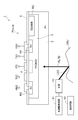
- FIG. 1 is a plan view of a distance image sensor according to an embodiment.
- FIG. 2 is a diagram showing a cross-sectional configuration of each pixel of the distance image sensor shown in FIG. 1 and a light source unit.
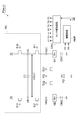
- FIG. 3 is a circuit diagram of each pixel of the distance image sensor shown in FIG.
- FIG. 4 is a diagram for explaining the operation of the distance image sensor according to the embodiment.
- FIG. 5 is an operation explanatory diagram of the distance image sensor according to the embodiment.
- FIG. 6 is an operation explanatory diagram of the distance image sensor according to the embodiment.
- FIG. 7 is an explanatory diagram of the operation of the distance image sensor according to the embodiment.
- FIG. 8 is an operation explanatory diagram of the distance image sensor according to the embodiment.
- FIG. 9 is an operation explanatory diagram of the distance image sensor according to the embodiment.
- FIG. 10 is an operation explanatory diagram of the distance image sensor according to the embodiment.
- FIG. 11 is an explanatory diagram of the operation of the distance image sensor according to the embodiment.
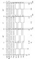
- FIG. 12 is a first timing chart of the distance image sensor according to the embodiment.
- FIG. 13 is a second timing chart of the distance image sensor according to the embodiment.
- FIG. 14 is a third timing chart of the distance image sensor according to the embodiment.
- FIG. 15 is a fourth timing chart of the distance image sensor according to the embodiment.
- FIG. 16 is a fifth timing chart of the distance image sensor according to the embodiment.
- FIG. 17 is a sixth timing chart of the distance image sensor according to the embodiment.
- FIG. 18 is a seventh timing chart of the distance image sensor according to the embodiment.
- FIG. 19 is an eighth timing chart of the distance image sensor according to the embodiment.
- FIG. 1 is a plan view of a distance image sensor according to an embodiment.
- the distance image sensor 1 includes an imaging region IMR formed on the semiconductor substrate 2, a sensor driving circuit DRV that drives the imaging region IMR, and an amplification circuit AMP that amplifies the output of the imaging region IMR.
- the imaging region IMR includes a plurality of pixels P (m, n) arranged in a one-dimensional or two-dimensional manner on the semiconductor substrate 2. In the drawing, m rows and n columns of pixels P (m, n) are shown (m and n are natural numbers).
- the imaging region IMR detects the reflected light of the emitted light to the object for each pixel, and the distance for each pixel of the image of the object is obtained from the phase difference between the emitted light and the reflected light for each pixel.
- This distance image sensor 1 is a charge distribution type distance image sensor, and obtains a phase difference corresponding to the distance according to the ratio of the amount of charge distributed to two locations in each pixel.
- FIG. 2 is a diagram showing a cross-sectional configuration of each pixel of the distance image sensor shown in FIG. 1 and a light source unit.
- the light source unit includes a light source 10 such as a laser or a light emitting diode, a light source drive circuit 11 that drives the light source 10 at a high frequency, and a control circuit 12 that outputs a drive clock of the light source drive circuit 11.
- the light source 10 emits a modulated signal that has been subjected to light intensity modulation of a square wave or a sine wave.
- a square wave or sine wave modulation signal is also output from the sensor drive circuit DRV shown in FIG. 1, and the modulation signals from the sensor drive circuit DRV are out of phase with each other. This is applied to the transfer electrodes TX1 and TX2.
- the emitted light LED from the light source 10 is irradiated on the object OBJ, reflected on the surface of the object OBJ, and reflected on the pixels P (m, n) in the imaging region IMR of the distance image sensor 1 as reflected light RLTD. Incident from the back side of the substrate.
- An imaging lens (not shown) is disposed in front of the light incident surface.
- the semiconductor substrate 2 is thinned and preferably has a thickness of 50 ⁇ m or less to constitute a back-illuminated distance image sensor.
- the present invention can also be applied to the surface incidence type distance image sensor 1 without reducing the thickness of the semiconductor substrate 2.
- Each pixel P (m, n) of the distance image sensor 1 is formed in a surface region of a high-concentration P-type (second conductivity type) semiconductor substrate 2 at a lower concentration than the semiconductor substrate (second conductivity type).
- a pair of high-concentration N-type (first conductivity type) semiconductor regions charge storage regions: floating diffusion regions
- fd1 and fd2 formed on the surface side of the semiconductor region 3.
- An insulating layer 5 is formed on the surface of the semiconductor substrate, and a photogate electrode PG is formed on the P-type semiconductor region 3 between the storage regions fd1 and fd2 via the insulating layer 5,
- the light detection region 4 immediately below the photogate electrode. The potential of the light detection region 4 can be controlled by the voltage applied to the photogate electrode PG.
- the signal extraction electrodes Vfd1 and Vfd2 are electrically connected to the storage regions fd1 and fd2, respectively. Further, the transfer electrodes TX1 and TX2 are located between the photogate electrode PG and the signal extraction electrodes Vfd1 and Vfd2.
- An N-type semiconductor has electrons as carriers in an electrically neutral state, and is positively ionized when carriers are removed. That is, the high-concentration N-type accumulation regions fd1 and fd2 are greatly recessed downward to constitute a potential well.
- a slight positive DC potential is applied to the photogate electrode PG as necessary.
- hole electron pairs are generated in response to the incidence of light.
- TX1 and TX2 functioning as the gate electrodes
- TX1 and TX2 The potential of the region immediately below becomes an intermediate value between the potential of the light detection region 4 and the potentials of the storage regions fd1 and fd2, and a potential step from the light detection region 4 to the storage regions fd1 and fd2 is formed. Electrons fall and accumulate in the potential well of fd2.
- This structure employs a structure in which electrodes are provided on the storage regions fd1 and fd2 and a signal is taken out. However, a high-concentration region for signal extraction is separately provided next to the storage regions fd1 and fd2. It is also possible to place another transfer electrode on the region between the regions fd1 and fd2 and provide an electrode on the high concentration region to extract a signal.
- the symbols Vfd1 and Vfd1 are signal extraction electrodes, and also indicate the voltages applied between these electrodes and the ground potential
- symbols TX1 and TX2 Is a transfer electrode and also indicates a transfer voltage applied between these and the ground potential.
- Reference numeral PG denotes a photogate electrode and also indicates a DC voltage applied between these and the ground potential.
- the semiconductor region 3 is connected to the ground potential.
- the charges extracted from the signal extraction electrodes Vfd1 and Vfd2 are read out by the read circuit RC formed in the semiconductor region 3.
- the read circuit is not limited to the semiconductor region 3 and may be formed on the semiconductor substrate 2.
- FIG. 3 is a circuit diagram of each pixel of the distance image sensor shown in FIG.
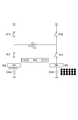
- Each pixel P (m, n) includes a light receiving region (photodiode PD) that generates a charge in response to incident reflected light, and a first storage region fd1 and a second storage region fd2 adjacent to the photodiode PD. It has.
- the first transfer electrode TX1 and the second transfer electrode TX2 control the inflow of charges into the first storage region fd1 and the second storage region fd2, respectively.
- a capacitor C1 is electrically connected between the electrodes Vfd1 and Vfd2 of the first and second accumulation regions fd1 and fd2 via switches ⁇ 1 and ⁇ 2 made of transistors, respectively.
- the first switch ⁇ 1 is interposed between the first terminal of the capacitor C1 (right terminal in the drawing: node VA) and the first storage region fd1, and the second switch ⁇ 2 is connected to the second terminal of the capacitor C1 ( It is interposed between the left terminal in the drawing: node VB) and the second accumulation region fd2.
- a third switch ⁇ 1r made of a transistor is interposed between the second terminal (terminal on the left side of the drawing: node VB) of the capacitor C1 and the positive reference potential Vr.
- a fourth switch ⁇ 2r is interposed between the first terminal (right terminal in the drawing: node VA) of the capacitor C1 and the reference potential Vr.
- the symbols ⁇ 1, ⁇ 2, ⁇ 1r, and ⁇ 2r indicate switches and also indicate voltages applied between the switches and the ground.
- Symbols VA and VB indicate nodes, and also indicate voltages between these nodes located at both ends of the capacitor C1 and the ground potential.
- parasitic capacitances Cfd1 and Cfd2 are interposed between the storage regions fd1 and fd2.
- Various signal voltages ⁇ 1, ⁇ 1r, ⁇ 2, ⁇ 2r, TX1, TX2, and PG are output from the sensor drive circuit DRV.
- the signal voltages ⁇ 1, ⁇ 1r, ⁇ 2, and ⁇ 2r are respectively applied to the control terminals of the switches ⁇ 1, ⁇ 1r, ⁇ 2, and ⁇ 2r made of transistors (a gate electrode for a field effect transistor and a base electrode for a bipolar transistor).
- the Transfer voltages TX1 and TX2, which are reverse phase signals, are respectively applied to transfer electrodes TX1 and TX2 constituting the gate electrode of the MOS transistor.
- the DC voltage PG is supplied to the photogate electrode PG.
- a region having a lower potential than the photodetection region 4 immediately below the photogate electrode PG is formed immediately below the transfer electrode, and thus a storage region having a lower potential than the region immediately below the transfer electrode. Electrons generated in the photodiode PD are transferred to and flow into fd1 and fd2.
- the charges are transferred to the capacitor C1.
- Charges derived from background light are also accumulated in the accumulation regions fd1 and fd2, but the amount of charge derived from the background light can be considered to be the same in both the accumulation regions fd1 and fd2, and this is regarded as the capacitor C1.
- These charges are canceled when transferred to both terminals. Therefore, in order to obtain the charge amount of the signal component, the charges accumulated in the accumulation regions fd1 and fd2 may be transferred to the single capacitor C1.
- the voltages VA and VB at both terminals of the capacitor C1 are input to the amplifier circuit AMP, and the output of the amplifier circuit AMP is input to the control circuit 12.
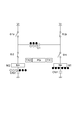
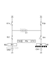
- 4 to 11 are operation explanatory views of the distance image sensor according to the embodiment, and schematically show only the portions necessary for the operation description.
- FIG. 4 shows a state in which all the switches ⁇ 1, ⁇ 1r, ⁇ 2, and ⁇ 2r are turned off after resetting, and no charge is present in the pixel.
- FIG. 5 shows a state where the switches ⁇ 1 and ⁇ 1r are turned on and ⁇ 2 and ⁇ 2r are turned off when light is incident directly below the photogate electrode PG and electrons as carriers are generated.
- Black circles in the figure indicate electrons flowing into the right accumulation region fd1
- white circles in the figure indicate electrons flowing into the left accumulation region fd2.
- 12 charges flow into the right side and 6 charges flow into the left side since the timing of the return light is delayed from the emission timing, it is assumed that 12 charges flow into the right side and 6 charges flow into the left side. Note that these charge amounts include components derived from background light.
- the charge flowing into the right accumulation region fd1 flows into one terminal of the capacitor C1 via the switch ⁇ 1, and the charge is divided.
- all the switches ⁇ 1, ⁇ 1r, ⁇ 2, and ⁇ 2r are turned off, and the electric charge remains in one terminal of the capacitor C1.
- FIG. 7 shows a state where the switches ⁇ 1 and ⁇ 1r are turned off and ⁇ 2 and ⁇ 2r are turned on.
- the charge accumulated in the left accumulation region fd2 is divided and flows into the other terminal of the capacitor C1, and the charge is divided.
- the charge accumulated on the right side of the capacitor C1 becomes a charge of opposite polarity accumulated at the opposite terminal. That is, as shown in FIG. 8, the charges accumulated on the right side of the capacitor C1 and the charges accumulated in the left accumulation region fd2 cancel each other and disappear, and only six charges are accumulated in the right accumulation region fd1. Remains.
- FIG. 9 shows a state in which, after that, 12 additional charges flow into the right accumulation region fd1 and 6 charges flow into the left accumulation region fd2 in response to the incidence of light.
- the total number of accumulated charges on the right side is 18. Since the switch ⁇ 2 is connected, the charge is divided and three charges flow into the left terminal of the capacitor C1.
- FIG. 10 shows a state in which the switch ⁇ 2r is turned off from the state of FIG. 9, and the state of FIG. 9 is maintained.
- FIG. 11 shows a state in which the switches ⁇ 1 and ⁇ 2 are then turned on and the charge accumulated in the right accumulation region fd1 is transferred to the capacitor C1, and the accumulated charge amount is redistributed according to the capacitor capacity. ing.
- the ratio of the left and right charge amounts is 2: 6.
- voltages VA and VB (Vfd1 and Vfd2) across the capacitor C1 are read out.
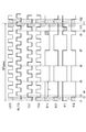
- FIG. 12 is a first timing chart of the distance image sensor according to the embodiment.
- the period from the current reset start time t1 to the next reset start time t9 is defined as one unit detection period (1 Phase). Between times t1 and t2, all the switches ⁇ 1r, ⁇ 2r, ⁇ 1, and ⁇ 2 are turned on, and the capacitor C1 and the storage regions fd1 and fd2 are reset to the initial state.
- a period between time t2 and time t5 is defined as one transfer period T to the capacitor, and switches ⁇ 1r and ⁇ 1 are applied while applying transfer voltages TX1 and TX2 composed of opposite-phase square waves to the transfer electrodes TX1 and TX2. Is turned on (high level), and the switches ⁇ 2r and ⁇ 2 are turned off (low level), so that the charge accumulated in the right accumulation region fd1 is transferred to the right terminal of the capacitor C1.
- the switches ⁇ 1r and ⁇ 1 are turned OFF (low level) while applying the transfer voltages TX1 and TX2 made of square waves of opposite phases to the transfer electrodes TX1 and TX2.
- the switches ⁇ 2r and ⁇ 2 are turned on (high level) to transfer the charge accumulated in the left accumulation region fd2 to the other terminal of the capacitor C1. Note that, when this switch is switched, the overlapping charge components are canceled out.
- the signal is read out in the period from time t8 to t9. Then, reset is performed again at the next time t9 to t10. In signal reading, the switches ⁇ 1 and ⁇ 2 are turned on, and ⁇ 1r and ⁇ 2r are turned off.
- an intensity signal LED of light emitted from the light source and an intensity signal RLTD of reflected light are shown.
- these waveforms are shown as square waves for simplification.
- the delay time of the reflected light with respect to the emitted light corresponds to the distance to the object. That is, the period from the time t2 to the time t3 is the time during which the light travels the reciprocating distance from the light source to the object.
- the drive signal to the light source is a square wave, and the rise and fall times thereof coincide with the rise and fall times of the transfer voltage TX1.
- Q1 be the amount of charge transferred into the right accumulation region fd1 when the transfer voltage TX1 is high level
- Q2 be the amount of charge transferred into the left accumulation region fd2 when the transfer voltage TX2 is high level.
- a delay time is generated between the emitted light and the reflected light by the ratio of the charge amount Q2 to the total charge amount (Q1 + Q2), which corresponds to twice the distance L to the object.
- the detection accuracy is improved by integrating the charges.
- the drive circuit DRV sets a reset period (time t1 to t2) in which all the switches ( ⁇ 1, ⁇ 2, ⁇ 1r, ⁇ 2r) are turned on at the first time of one cycle (1 Phase), and one cycle (1 Phase) ),
- the first period (time t2 to t5, time t6 to t7: T1) and the second period (time t5 to t6, time t7 to t8: T2) are alternately set. .
- both of the switches ( ⁇ 1, ⁇ 1r) are turned on, both of the switches ( ⁇ 2, ⁇ 2r) are turned off, and in the second period (T2), the switches ( ⁇ 1, ⁇ 1r) Both are turned OFF, both the second and fourth switches ( ⁇ 2, ⁇ 2r) are turned ON, and in one cycle (1 Phase), the transfer electrodes TX1 and TX2 are synchronized with the modulation signal LED of the emitted light and are opposite to each other. Phase modulation signals TX1, TX2 are provided.
- Noise based on the light quantum increases at the square root of the exposure light quantity, and the signal component increases proportionally. Therefore, as the exposure time is increased, the ratio of the signal component increases, and the signal to noise ratio increases. Will improve. Therefore, as the charges distributed in the first and second accumulation regions fd1 and fd2 are integrated by the transfer electrodes TX1 and TX2, the signal-to-noise ratio is improved, and an accurate distance image (luminance image) can be obtained. it can.
- the charge integration for a certain period is performed in the storage regions fd1 and fd2, and at the same time or after the integration, the charge integrated in the storage region fd1 is changed to the first.
- the charge connected to the right terminal VA of the capacitor C1 and integrated in the storage region fd2 is connected to the left terminal VB of the capacitor C1 in the second period (T2), and the capacitor C1.
- the charge components included in both storage regions fd1 and fd2, that is, the background light components are canceled out.
- each storage region fd1, fd2 is connected only to a single capacitor C1
- the pixel size can be reduced to improve the spatial resolution, and the storage regions fd1, fd2 Since the transferred charges are integrated, the signal-to-noise ratio is improved, and the number of times of switching when the switches Q1 and Q2 are transferred to the capacitor C1 is reduced. Accurate distance can be calculated by accumulating electric charge according to the distance and detecting the amount of electric charge (voltage corresponding thereto).
- FIG. 13 is a second timing chart of the distance image sensor according to the embodiment.
- the signal is read during a period between time t9 and time t10, and the other configurations are the same as those in the first timing chart. That is, the signal is read out with all the switches ⁇ 1, ⁇ 2, ⁇ 1r, and ⁇ 2r turned off.
- FIG. 14 is a third timing chart of the distance image sensor according to the embodiment.
- timing chart a period in which both the transfer voltages TX1 and TX2 are turned off is set between time t8 and time t9, and a signal is read during this period. It is the same as the timing chart.
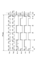
- FIG. 15 is a fourth timing chart of the distance image sensor according to the embodiment. This timing chart is a modification of the first timing chart and includes a dummy switching period.
- the switching times of the first and second switches ( ⁇ 1, ⁇ 2) in the period (from time t2 to time t11) after the end of the reset period within one cycle (1 Phase) become equal.
- the first or second switch ( ⁇ 1, ⁇ 2) is additionally switched (in this example, the switch ⁇ 1 is turned OFF and ON at time t9 and time t10).
- the number of times of switching becomes equal and the offset is canceled out, so that a more accurate distance image can be obtained.
- the third or fourth switch is set so that the number of times the third and fourth switches ( ⁇ 1r, ⁇ 2r) switch in the period (from time t2 to time t11) after the end of the reset period within one cycle (1 Phase) becomes equal.
- 4 switches ( ⁇ 1r, ⁇ 2r) are additionally switched (in this example, the switch ⁇ 1r is turned on and off at time t8 and time t9).
- the number of times of switching becomes equal and the offset is canceled out, so that a more accurate distance image can be obtained.
- FIG. 16 is a fifth timing chart of the distance image sensor according to the embodiment. This timing chart is a modification of the second timing chart and includes a dummy switching period.
- the driving circuit DRV has the same number of switching times of the first and second switches ( ⁇ 1, ⁇ 2) in the period (from time t2 to time t10) after the end of the reset period within one cycle (1 Phase).
- the first or second switch ( ⁇ 1, ⁇ 2) is additionally switched (in this example, the switch ⁇ 1 is turned OFF and ON at time t9 and time t10).
- the number of times of switching becomes equal and the offset is canceled out, so that a more accurate distance image can be obtained.
- FIG. 17 is a sixth timing chart of the distance image sensor according to the embodiment. This timing chart is a modification of the first timing chart and includes a dummy switching period.
- the driving circuit DRV has the same number of switching times of the first and second switches ( ⁇ 1, ⁇ 1r) in the period (from time t2 to time t9) after the end of the reset period within one cycle (1 Phase).
- the first or second switch ( ⁇ 1, ⁇ 1r) is additionally switched (in this example, at the time immediately after the reset period (t1 to t2), the switches ⁇ 1 and ⁇ 1r are turned OFF and ON. is doing).
- additional switching hereinafter referred to as “dummy switching”
- the number of times of switching becomes equal and the offset is canceled out, so that a more accurate distance image can be obtained.
- Times t8 to t9 are signal readout periods, and times t9 to t10 are the next reset periods. First, all switches are reset and accumulation is started.
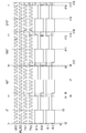
- FIG. 18 is a seventh timing chart of the distance image sensor according to the embodiment.
- each storage region fd1 By taking the difference between the charges (according to the voltage) accumulated in fd2, the offset component can be canceled together with the background light component. Thereby, an accurate distance can be calculated.
- the drive circuit DRV gives signals as follows.
- the modulation signal TX1 is given to the first transfer electrode at a timing having a phase difference of 0 ° from the modulation signal LED of the emitted light within a specific period (time t1 to t5), and the second transfer electrode.
- a modulation signal TX2 having a phase opposite to that of the modulation signal TX1 applied to the first transfer electrode is applied.
- the modulation signal TX1 is given to the first transfer electrode at a timing having a phase difference of 90 ° with the modulation signal LED of the emitted light, and the second transfer electrode In addition, a modulation signal TX2 having a phase opposite to that of the modulation signal TX1 applied to the first transfer electrode is applied.
- the modulation signal TX1 is given to the first transfer electrode at a timing having a phase difference of 180 ° from the modulation signal LED of the emitted light, and the second transfer A modulation signal TX2 having a phase opposite to that of the modulation signal TX1 applied to the first transfer electrode is applied to the electrode.
- the modulation signal TX1 is applied to the first transfer electrode at a timing having a phase difference of 270 ° from the modulation signal LED of the emitted light.
- the second transfer electrode is supplied with a modulation signal TX2 having a phase opposite to that of the modulation signal TX1 applied to the first transfer electrode.
- the order of the first period (T1: period in which ⁇ 1, ⁇ 1r is ON) and the second period (T2: period in which ⁇ 2, ⁇ 2r is ON) in one cycle of (a) to (d) above. are the same.
- the offset can be canceled and the distance can be obtained. . That is, assuming that the same amount of offset is superimposed on the voltages Vfd1 and Vfd2 of each phase, the influence of the offset can be reduced by taking the difference between the voltages Vfd1 and Vfd2.
- Vfd (0 °) Vfd1 (0 °) ⁇ Vfd1 (180 °)
- Vfd (90 °) Vfd1 (90 °) ⁇ Vfd1 (270 °)
- Vfd (180 °) Vfd2 (0 °) ⁇ Vfd2 (180 °)
- Vfd (270 °) Vfd2 (90 °) ⁇ Vfd2 (270 °)
- V1
- V2
- the total amount of signal Vtotal is V1 + V2, and the distance traveled by light during a period including four phases (t1 to t17) is given by V1 / Vtotal.
- FIG. 19 is an eighth timing chart of the distance image sensor according to the embodiment.
- Times t1 to t2, t5 to t6, t9 to t10, t13 to t14, t17 to t18 are reset periods, and time t4 to t5, t8 to t9, t12 to t13, and t16 to t17 are signal readout periods.
- this timing chart only two phase differences of 0 ° and 90 ° are used, but the order of ⁇ 1 and ⁇ 2 is reversed between the first half and the second half of the detection period (t1 to t18).
- the distance image sensor drive circuit DRV gives signals as follows.
- the modulation signal TX1 is given to the first transfer electrode at a timing having a phase difference of 0 ° from the modulation signal LED of the emitted light within a specific period (time t1 to t5), and the second transfer electrode
- a modulation signal TX2 having a phase opposite to that of the modulation signal TX1 applied to the first transfer electrode is applied.
- the modulation signal TX1 is given to the first transfer electrode at a timing having a phase difference of 90 ° with the modulation signal LED of the emitted light, and the second transfer electrode In addition, a modulation signal TX2 having a phase opposite to that of the modulation signal TX1 applied to the first transfer electrode is applied.
- the modulation signal TX1 is given to the first transfer electrode at a timing having a phase difference of 0 ° from the modulation signal LED of the emitted light, and the second transfer A modulation signal TX2 having a phase opposite to that of the modulation signal TX1 applied to the first transfer electrode is applied to the electrode.
- the modulation signal TX1 is given to the first transfer electrode at a timing having a phase difference of 90 ° with the modulation signal LED of the emitted light,
- the second transfer electrode is supplied with a modulation signal TX2 having a phase opposite to that of the modulation signal TX1 applied to the first transfer electrode.
- T1 period in which ⁇ 1, ⁇ 1r is ON
- T2 period in which ⁇ 2, ⁇ 2 are ON
- the order of the first period T1 and the second period T2 in one cycle of the above (c) and (d) is opposite to the case of (a) and (b) above.
- the two phases (a) and (b) described above and the phase of charge transfer to the capacitor C1 are different from each other in the phases (c) and (d).
- the offset component can be canceled together with the background light component. Thereby, an accurate distance can be calculated.
- the distance image sensor of the present invention can obtain an accurate distance image.
- Vfd1 and Vfd2 in each phase are indicated as Vfd1 (phase) and Vfd2 (phase)
- the following difference values are obtained in order to remove these variations and DC components.
- Vfd1 and Vfd2 indicate voltages in the first half periods (a) and (b)
- Vfd1 ′ and Vfd2 ′ indicate these voltages in the second half periods (c) and (d).
- Vfd (0 °) Vfd1 (0 °) ⁇ Vfd2 (0 °)
- Vfd (90 °) Vfd1 (90 °) ⁇ Vfd2 (90 °)
- Vfd ′ (0 °) Vfd1 ′ (0 °) ⁇ Vfd2 ′ (0 °)
- Vfd ′ (90 °) Vfd1 ′ (90 °) ⁇ Vfd2 ′ (90 °)
- L1 Vfd (0 °) / (Vfd (0 °) + Vfd (90 °))
- L2 Vfd ′ (0 °) / (Vfd ′ (0 °) + Vfd ′ (90 °))
- SYMBOLS 1 Distance image sensor, IMR ... Imaging region, PD ... Light receiving region, fd1, fd2 ... Accumulation region, TX1, TX2 ... Transfer electrode, C1 ... Capacitor, ⁇ 1 ... First switch, ⁇ 2... Second switch, ⁇ 1r... Third switch, ⁇ 2r... Fourth switch, DRV.
Landscapes
- Engineering & Computer Science (AREA)
- Physics & Mathematics (AREA)
- General Physics & Mathematics (AREA)
- Computer Networks & Wireless Communication (AREA)
- Radar, Positioning & Navigation (AREA)
- Remote Sensing (AREA)
- Electromagnetism (AREA)
- Power Engineering (AREA)
- Spectroscopy & Molecular Physics (AREA)
- Optical Radar Systems And Details Thereof (AREA)
- Measurement Of Optical Distance (AREA)
- Solid State Image Pick-Up Elements (AREA)
- Transforming Light Signals Into Electric Signals (AREA)
Abstract
Description
・Vfd1=(1/(3×C))・((5/2)×Q1+2×Q2)
・Vfd2=(1/(3×C))・((1/2)×Q1+4×Q2)
・VOUT=Vfd1-Vfd2=n(Q1-Q2)/3C
(b)別の一周期(時刻t5~t9)内において、出射光の変調信号LEDと90°の位相差を有するタイミングで、第1の転送電極に変調信号TX1を与え、第2の転送電極に、第1の転送電極に与えられる変調信号TX1とは逆相の変調信号TX2を与えている。
(c)更に別の一周期(時刻t9~t13)内において、出射光の変調信号LEDと180°の位相差を有するタイミングで、第1の転送電極に変調信号TX1を与え、第2の転送電極に、第1の転送電極に与えられる変調信号TX1とは逆相の変調信号TX2を与えている。
(d)上記とは異なる別の一周期(時刻t13~t17)内において、出射光の変調信号LEDと270°の位相差を有するタイミングで、第1の転送電極に変調信号TX1を与え、第2の転送電極に、第1の転送電極に与えられる変調信号TX1とは逆相の変調信号TX2を与えている。
Vfd(0°)=Vfd1(0°)-Vfd1(180°)
Vfd(90°)=Vfd1(90°)-Vfd1(270°)
Vfd(180°)=Vfd2(0°)-Vfd2(180°)
Vfd(270°)=Vfd2(90°)-Vfd2(270°)
V1=|Vfd(0°)-Vfd(180°)|
V2=|Vfd(90°)-Vfd(270°)|
信号の総量VtotalをV1+V2として、4つの位相を含む期間(t1~t17)に光が進む距離はV1/Vtotalで与えられる。
(a)特定の一周期(時刻t1~t5)内において、出射光の変調信号LEDと0°の位相差を有するタイミングで、第1の転送電極に変調信号TX1を与え、第2の転送電極に、第1の転送電極に与えられる変調信号TX1とは逆相の変調信号TX2を与えている。
(b)別の一周期(時刻t5~t9)内において、出射光の変調信号LEDと90°の位相差を有するタイミングで、第1の転送電極に変調信号TX1を与え、第2の転送電極に、第1の転送電極に与えられる変調信号TX1とは逆相の変調信号TX2を与えている。
(c)更に別の一周期(時刻t9~t13)内において、出射光の変調信号LEDと0°の位相差を有するタイミングで、第1の転送電極に変調信号TX1を与え、第2の転送電極に、第1の転送電極に与えられる変調信号TX1とは逆相の変調信号TX2を与えている。
(d)上記とは異なる別の一周期(時刻t13~t17)内において、出射光の変調信号LEDと90°の位相差を有するタイミングで、第1の転送電極に変調信号TX1を与え、第2の転送電極に、第1の転送電極に与えられる変調信号TX1とは逆相の変調信号TX2を与えている。
Vfd(0°)=Vfd1(0°)-Vfd2(0°)
Vfd(90°)=Vfd1(90°)-Vfd2(90°)
Vfd’(0°)=Vfd1’(0°)-Vfd2’(0°)
Vfd’(90°)=Vfd1’(90°)-Vfd2’(90°)
L1=Vfd(0°)/(Vfd(0°)+Vfd(90°))
L2=Vfd’(0°)/(Vfd’(0°)+Vfd’(90°))
Claims (4)
- 対象物への出射光の反射光を受光する撮像領域と、前記撮像領域を駆動する駆動回路と、を備えた距離画像センサであって、
前記撮像領域は、
半導体基板上に一次元又は二次元状に配置された複数の画素を備え、
個々の画素は、
受光領域と、
前記受光領域に隣接した第1及び第2の蓄積領域と、
前記第1及び第2の蓄積領域への電荷の流入をそれぞれ制御する第1及び第2の転送電極と、
前記第1及び第2の蓄積領域間に電気的に接続されたキャパシタと、
前記キャパシタの第1端子と前記第1の蓄積領域との間に介在する第1のスイッチと、
前記キャパシタの第2端子と前記第2の蓄積領域との間に介在する第2のスイッチと、
前記キャパシタの前記第2端子と基準電位との間に介在する第3のスイッチと、
前記キャパシタの前記第1端子と前記基準電位との間に介在する第4のスイッチと、を備え、
前記駆動回路は、
前記第1、第2、第3及び第4のスイッチを一周期の初めの時刻において全てONさせるリセット期間を設定し、一周期内において、第1の期間及び第2の期間を交互に設定し、
前記第1の期間では、前記第1及び第3のスイッチの双方をONし、第2及び第4スイッチの双方をOFFし、
前記第2の期間では、前記第1及び第3のスイッチの双方をOFFし、第2及び第4スイッチの双方をONし、
前記一周期内において、前記第1及び第2の転送電極に、前記出射光の変調信号に同期し、互いに逆相の変調信号を与える、ことを特徴とする距離画像センサ。 - 前記駆動回路は、前記一周期内における前記リセット期間終了時以後の第1及び第2のスイッチのスイッチング回数が等しくなるように、第1又は第2のスイッチを付加的にスイッチングすることを特徴とする請求項1に記載の距離画像センサ。
- 前記駆動回路は、
(a)特定の一周期内において、前記出射光の変調信号と0°の位相差を有するタイミングで、前記第1の転送電極に変調信号を与え、前記第2の転送電極に、前記第1の転送電極に与えられる変調信号とは逆相の変調信号を与え、
(b)別の一周期内において、前記出射光の変調信号と90°の位相差を有するタイミングで、前記第1の転送電極に変調信号を与え、前記第2の転送電極に、前記第1の転送電極に与えられる変調信号とは逆相の変調信号を与え、
(c)更に別の一周期内において、前記出射光の変調信号と180°の位相差を有するタイミングで、前記第1の転送電極に変調信号を与え、前記第2の転送電極に、前記第1の転送電極に与えられる変調信号とは逆相の変調信号を与え、
(d)上記とは異なる別の一周期内において、前記出射光の変調信号と270°の位相差を有するタイミングで、前記第1の転送電極に変調信号を与え、前記第2の転送電極に、前記第1の転送電極に与えられる変調信号とは逆相の変調信号を与え、
前記(a)~(d)の一周期内における前記第1の期間と前記第2の期間の順序は同一である、ことを特徴とする請求項1に記載の距離画像センサ。 - 前記駆動回路は、
(a)特定の一周期内において、前記出射光の変調信号と0°の位相差を有するタイミングで、前記第1の転送電極に変調信号を与え、前記第2の転送電極に、前記第1の転送電極に与えられる変調信号とは逆相の変調信号を与え、
(b)別の一周期内において、前記出射光の変調信号と90°の位相差を有するタイミングで、前記第1の転送電極に変調信号を与え、前記第2の転送電極に、前記第1の転送電極に与えられる変調信号とは逆相の変調信号を与え、
(c)更に別の一周期内において、前記出射光の変調信号と0°の位相差を有するタイミングで、前記第1の転送電極に変調信号を与え、前記第2の転送電極に、前記第1の転送電極に与えられる変調信号とは逆相の変調信号を与え、
(d)上記とは異なる別の一周期内において、前記出射光の変調信号と90°の位相差を有するタイミングで、前記第1の転送電極に変調信号を与え、前記第2の転送電極に、前記第1の転送電極に与えられる変調信号とは逆相の変調信号を与え、
前記(a)及び(b)の一周期内における前記第1の期間と前記第2の期間の順序は同一であり、
前記(c)及び(d)の一周期内における前記第1の期間と前記第2の期間の順序は、前記(a)及び(b)の場合とは逆である、ことを特徴とする請求項1に記載の距離画像センサ。
Priority Applications (3)
| Application Number | Priority Date | Filing Date | Title |
|---|---|---|---|
| EP11747398.3A EP2541275B1 (en) | 2010-02-26 | 2011-02-23 | Range image sensor |
| KR1020127018895A KR101751090B1 (ko) | 2010-02-26 | 2011-02-23 | 거리 화상 센서 |
| US13/578,048 US9081095B2 (en) | 2010-02-26 | 2011-02-23 | Range image sensor |
Applications Claiming Priority (2)
| Application Number | Priority Date | Filing Date | Title |
|---|---|---|---|
| JP2010-043467 | 2010-02-26 | ||
| JP2010043467A JP5302244B2 (ja) | 2010-02-26 | 2010-02-26 | 距離画像センサ |
Publications (1)
| Publication Number | Publication Date |
|---|---|
| WO2011105438A1 true WO2011105438A1 (ja) | 2011-09-01 |
Family
ID=44506840
Family Applications (1)
| Application Number | Title | Priority Date | Filing Date |
|---|---|---|---|
| PCT/JP2011/054006 Ceased WO2011105438A1 (ja) | 2010-02-26 | 2011-02-23 | 距離画像センサ |
Country Status (5)
| Country | Link |
|---|---|
| US (1) | US9081095B2 (ja) |
| EP (1) | EP2541275B1 (ja) |
| JP (1) | JP5302244B2 (ja) |
| KR (1) | KR101751090B1 (ja) |
| WO (1) | WO2011105438A1 (ja) |
Cited By (4)
| Publication number | Priority date | Publication date | Assignee | Title |
|---|---|---|---|---|
| EP2690464A1 (en) * | 2012-07-24 | 2014-01-29 | Samsung Electronics Co., Ltd | Depth sensing apparatus and method |
| EP2799906A4 (en) * | 2011-12-28 | 2015-08-26 | Hamamatsu Photonics Kk | DISTANCE METER |
| WO2021070212A1 (ja) * | 2019-10-07 | 2021-04-15 | 株式会社ブルックマンテクノロジ | 距離画像撮像装置及び距離画像撮像方法 |
| CN113411519A (zh) * | 2020-03-16 | 2021-09-17 | 爱思开海力士有限公司 | 图像感测设备及其操作方法 |
Families Citing this family (26)
| Publication number | Priority date | Publication date | Assignee | Title |
|---|---|---|---|---|
| JP5616099B2 (ja) * | 2010-04-01 | 2014-10-29 | 浜松ホトニクス株式会社 | 距離センサ及び距離画像センサ |
| JP5932400B2 (ja) | 2012-03-02 | 2016-06-08 | 浜松ホトニクス株式会社 | 距離センサ及び距離画像センサ |
| US9134401B2 (en) * | 2012-03-27 | 2015-09-15 | Hamamatsu Photonics K. K. | Range sensor and range image sensor |
| KR101434916B1 (ko) * | 2014-02-18 | 2014-08-28 | 김태민 | 3차원 영상 정보를 얻기 위한 이미지센서 및 2차원 영상과 3차원 영상 정보의 정합 방법 |
| KR101434915B1 (ko) * | 2014-03-12 | 2014-08-28 | 김태민 | 위상별 광량을 누적하는 병렬 구조 이미지센서 |
| DE102014210177B3 (de) * | 2014-05-28 | 2015-07-16 | Ifm Electronic Gmbh | Lichtlaufzeitsensor |
| EP2955539B1 (en) | 2014-06-12 | 2018-08-08 | Delphi International Operations Luxembourg S.à r.l. | Distance measuring device |
| KR102285392B1 (ko) * | 2015-02-03 | 2021-08-04 | 삼성디스플레이 주식회사 | 센싱 장치, 표시장치, 및 전기적 신호 센싱 방법 |
| US10134926B2 (en) * | 2015-02-03 | 2018-11-20 | Microsoft Technology Licensing, Llc | Quantum-efficiency-enhanced time-of-flight detector |
| JP6524478B2 (ja) * | 2015-08-20 | 2019-06-05 | 株式会社Zmp | 距離センサー及びそれを用いた搬送用ロボット |
| US11131756B2 (en) * | 2015-09-29 | 2021-09-28 | Qualcomm Incorporated | LIDAR system with reflected signal strength measurement |
| JP6659447B2 (ja) | 2016-05-02 | 2020-03-04 | 浜松ホトニクス株式会社 | 距離センサ |
| JP6659448B2 (ja) | 2016-05-02 | 2020-03-04 | 浜松ホトニクス株式会社 | 距離センサ及び距離センサの駆動方法 |
| US10616519B2 (en) | 2016-12-20 | 2020-04-07 | Microsoft Technology Licensing, Llc | Global shutter pixel structures with shared transfer gates |
| US10389957B2 (en) | 2016-12-20 | 2019-08-20 | Microsoft Technology Licensing, Llc | Readout voltage uncertainty compensation in time-of-flight imaging pixels |
| EP3392675B1 (en) * | 2017-04-21 | 2021-03-10 | Melexis Technologies NV | Active pixel circuit for a time-of-flight system and method for operating the same |
| EP3499872B1 (en) * | 2017-12-15 | 2020-08-19 | ams AG | Pixel structure, image sensor device and system with pixel structure, and method of operating the pixel structure |
| KR102049845B1 (ko) | 2017-12-29 | 2019-11-28 | 충남대학교산학협력단 | 라이다용 시간-전압 변환기 및 라이다 |
| JP2021193759A (ja) * | 2018-09-14 | 2021-12-23 | ソニーセミコンダクタソリューションズ株式会社 | 固体撮像装置、放射線検出器及び放射線計測システム |
| KR102646902B1 (ko) | 2019-02-12 | 2024-03-12 | 삼성전자주식회사 | 거리 측정을 위한 이미지 센서 |
| WO2020166572A1 (ja) * | 2019-02-15 | 2020-08-20 | パナソニックセミコンダクターソリューションズ株式会社 | 撮像装置及び距離情報算出方法 |
| KR102427559B1 (ko) * | 2019-10-22 | 2022-08-01 | 주식회사 아모센스 | 거리센서 모듈 |
| WO2021168732A1 (en) * | 2020-02-27 | 2021-09-02 | Shenzhen Genorivision Technology Co., Ltd. | Radiation detectors with high pixel concentrations |
| CN114335033B (zh) * | 2020-09-30 | 2025-07-11 | 思特威(上海)电子科技股份有限公司 | 测距像素结构及tof图像传感器 |
| FR3115145B1 (fr) * | 2020-10-14 | 2023-06-02 | Commissariat Energie Atomique | Dispositif d'acquisition d'une image 2d et d'une image de profondeur d'une scene |
| FR3160285A1 (fr) * | 2024-03-15 | 2025-09-19 | Commissariat A L' Energie Atomique Et Aux Energies Alternatives | pixel de profondeur à capacité d’intégration commutable |
Citations (4)
| Publication number | Priority date | Publication date | Assignee | Title |
|---|---|---|---|---|
| JPH01301110A (ja) * | 1988-02-09 | 1989-12-05 | Ntt Technol Transfer Corp | 受光回路 |
| JPH10281868A (ja) | 1997-04-04 | 1998-10-23 | Shigeru Ando | 時間相関検出型イメージセンサおよび画像解析方法 |
| US6919549B2 (en) | 2003-04-11 | 2005-07-19 | Canesta, Inc. | Method and system to differentially enhance sensor dynamic range |
| JP2009047662A (ja) * | 2007-08-22 | 2009-03-05 | Hamamatsu Photonics Kk | 固体撮像装置及び距離画像測定装置 |
Family Cites Families (5)
| Publication number | Priority date | Publication date | Assignee | Title |
|---|---|---|---|---|
| US7176438B2 (en) | 2003-04-11 | 2007-02-13 | Canesta, Inc. | Method and system to differentially enhance sensor dynamic range using enhanced common mode reset |
| JP5395323B2 (ja) * | 2006-09-29 | 2014-01-22 | ブレインビジョン株式会社 | 固体撮像素子 |
| EP2116864A1 (en) * | 2008-05-09 | 2009-11-11 | Vrije Universiteit Brussel | TOF range finding with background radiation suppression |
| JP2009278241A (ja) * | 2008-05-13 | 2009-11-26 | Canon Inc | 固体撮像装置の駆動方法および固体撮像装置 |
| WO2010144616A1 (en) * | 2009-06-09 | 2010-12-16 | Mesa Imaging Ag | System for charge-domain electron subtraction in demodulation pixels and method therefor |
-
2010
- 2010-02-26 JP JP2010043467A patent/JP5302244B2/ja not_active Expired - Fee Related
-
2011
- 2011-02-23 WO PCT/JP2011/054006 patent/WO2011105438A1/ja not_active Ceased
- 2011-02-23 US US13/578,048 patent/US9081095B2/en active Active
- 2011-02-23 EP EP11747398.3A patent/EP2541275B1/en active Active
- 2011-02-23 KR KR1020127018895A patent/KR101751090B1/ko not_active Expired - Fee Related
Patent Citations (5)
| Publication number | Priority date | Publication date | Assignee | Title |
|---|---|---|---|---|
| JPH01301110A (ja) * | 1988-02-09 | 1989-12-05 | Ntt Technol Transfer Corp | 受光回路 |
| JPH10281868A (ja) | 1997-04-04 | 1998-10-23 | Shigeru Ando | 時間相関検出型イメージセンサおよび画像解析方法 |
| US6919549B2 (en) | 2003-04-11 | 2005-07-19 | Canesta, Inc. | Method and system to differentially enhance sensor dynamic range |
| JP2006523074A (ja) | 2003-04-11 | 2006-10-05 | カネスタ インコーポレイテッド | センサのダイナミックレンジを差分拡大する方法及びシステム |
| JP2009047662A (ja) * | 2007-08-22 | 2009-03-05 | Hamamatsu Photonics Kk | 固体撮像装置及び距離画像測定装置 |
Non-Patent Citations (1)
| Title |
|---|
| See also references of EP2541275A4 |
Cited By (7)
| Publication number | Priority date | Publication date | Assignee | Title |
|---|---|---|---|---|
| EP2799906A4 (en) * | 2011-12-28 | 2015-08-26 | Hamamatsu Photonics Kk | DISTANCE METER |
| US9151831B2 (en) | 2011-12-28 | 2015-10-06 | Hamamatsu Photonics K.K. | Distance measurement device |
| EP2690464A1 (en) * | 2012-07-24 | 2014-01-29 | Samsung Electronics Co., Ltd | Depth sensing apparatus and method |
| CN103581645A (zh) * | 2012-07-24 | 2014-02-12 | 三星电子株式会社 | 深度感测设备和方法 |
| US9137521B2 (en) | 2012-07-24 | 2015-09-15 | Samsung Electronics Co., Ltd. | Depth sensing apparatus and method |
| WO2021070212A1 (ja) * | 2019-10-07 | 2021-04-15 | 株式会社ブルックマンテクノロジ | 距離画像撮像装置及び距離画像撮像方法 |
| CN113411519A (zh) * | 2020-03-16 | 2021-09-17 | 爱思开海力士有限公司 | 图像感测设备及其操作方法 |
Also Published As
| Publication number | Publication date |
|---|---|
| US20120312966A1 (en) | 2012-12-13 |
| EP2541275A1 (en) | 2013-01-02 |
| JP2011179926A (ja) | 2011-09-15 |
| EP2541275B1 (en) | 2017-03-22 |
| EP2541275A4 (en) | 2013-08-28 |
| KR101751090B1 (ko) | 2017-06-26 |
| KR20130045833A (ko) | 2013-05-06 |
| JP5302244B2 (ja) | 2013-10-02 |
| US9081095B2 (en) | 2015-07-14 |
Similar Documents
| Publication | Publication Date | Title |
|---|---|---|
| JP5302244B2 (ja) | 距離画像センサ | |
| KR101348522B1 (ko) | 고체 촬상 장치 및 거리 화상 측정 장치 | |
| CN107852470B (zh) | 固体摄像装置的驱动方法 | |
| JP5395323B2 (ja) | 固体撮像素子 | |
| US9171985B2 (en) | Pixel circuit with controlled capacitor discharge time of flight measurement | |
| US9134401B2 (en) | Range sensor and range image sensor | |
| US20180176498A1 (en) | Global shutter pixel structures with shared transfer gates | |
| US10473782B2 (en) | Photoelectric conversion element, photoelectric conversion apparatus using the same, distance detection sensor, and information processing system | |
| JP5616099B2 (ja) | 距離センサ及び距離画像センサ | |
| JP2018006989A (ja) | 光学装置およびシステム | |
| JP2004264034A (ja) | 光検出装置 | |
| CN109643523B (zh) | 像素电路以及图像传感系统 | |
| US9053998B2 (en) | Range sensor and range image sensor | |
| JP6700687B2 (ja) | 光電変換デバイス、測距装置および情報処理システム | |
| Joboji et al. | A Range Finding Array Sensor Performing Correlated Calculations with a PN Code Modulation Light |
Legal Events
| Date | Code | Title | Description |
|---|---|---|---|
| 121 | Ep: the epo has been informed by wipo that ep was designated in this application |
Ref document number: 11747398 Country of ref document: EP Kind code of ref document: A1 |
|
| ENP | Entry into the national phase |
Ref document number: 20127018895 Country of ref document: KR Kind code of ref document: A |
|
| WWE | Wipo information: entry into national phase |
Ref document number: 13578048 Country of ref document: US |
|
| REEP | Request for entry into the european phase |
Ref document number: 2011747398 Country of ref document: EP |
|
| WWE | Wipo information: entry into national phase |
Ref document number: 2011747398 Country of ref document: EP |
|
| NENP | Non-entry into the national phase |
Ref country code: DE |