WO2011114562A1 - 走査信号線駆動回路およびそれを備えた表示装置 - Google Patents
走査信号線駆動回路およびそれを備えた表示装置 Download PDFInfo
- Publication number
- WO2011114562A1 WO2011114562A1 PCT/JP2010/068018 JP2010068018W WO2011114562A1 WO 2011114562 A1 WO2011114562 A1 WO 2011114562A1 JP 2010068018 W JP2010068018 W JP 2010068018W WO 2011114562 A1 WO2011114562 A1 WO 2011114562A1
- Authority
- WO
- WIPO (PCT)
- Prior art keywords
- node
- level
- electrode
- potential
- signal
- Prior art date
- Legal status (The legal status is an assumption and is not a legal conclusion. Google has not performed a legal analysis and makes no representation as to the accuracy of the status listed.)
- Ceased
Links
Images


Classifications
-
- G—PHYSICS
- G09—EDUCATION; CRYPTOGRAPHY; DISPLAY; ADVERTISING; SEALS
- G09G—ARRANGEMENTS OR CIRCUITS FOR CONTROL OF INDICATING DEVICES USING STATIC MEANS TO PRESENT VARIABLE INFORMATION
- G09G3/00—Control arrangements or circuits, of interest only in connection with visual indicators other than cathode-ray tubes
- G09G3/20—Control arrangements or circuits, of interest only in connection with visual indicators other than cathode-ray tubes for presentation of an assembly of a number of characters, e.g. a page, by composing the assembly by combination of individual elements arranged in a matrix no fixed position being assigned to or needed to be assigned to the individual characters or partial characters
- G09G3/34—Control arrangements or circuits, of interest only in connection with visual indicators other than cathode-ray tubes for presentation of an assembly of a number of characters, e.g. a page, by composing the assembly by combination of individual elements arranged in a matrix no fixed position being assigned to or needed to be assigned to the individual characters or partial characters by control of light from an independent source
- G09G3/36—Control arrangements or circuits, of interest only in connection with visual indicators other than cathode-ray tubes for presentation of an assembly of a number of characters, e.g. a page, by composing the assembly by combination of individual elements arranged in a matrix no fixed position being assigned to or needed to be assigned to the individual characters or partial characters by control of light from an independent source using liquid crystals
- G09G3/3611—Control of matrices with row and column drivers
- G09G3/3674—Details of drivers for scan electrodes
- G09G3/3677—Details of drivers for scan electrodes suitable for active matrices only
-
- G—PHYSICS
- G02—OPTICS
- G02F—OPTICAL DEVICES OR ARRANGEMENTS FOR THE CONTROL OF LIGHT BY MODIFICATION OF THE OPTICAL PROPERTIES OF THE MEDIA OF THE ELEMENTS INVOLVED THEREIN; NON-LINEAR OPTICS; FREQUENCY-CHANGING OF LIGHT; OPTICAL LOGIC ELEMENTS; OPTICAL ANALOGUE/DIGITAL CONVERTERS
- G02F1/00—Devices or arrangements for the control of the intensity, colour, phase, polarisation or direction of light arriving from an independent light source, e.g. switching, gating or modulating; Non-linear optics
- G02F1/01—Devices or arrangements for the control of the intensity, colour, phase, polarisation or direction of light arriving from an independent light source, e.g. switching, gating or modulating; Non-linear optics for the control of the intensity, phase, polarisation or colour
- G02F1/13—Devices or arrangements for the control of the intensity, colour, phase, polarisation or direction of light arriving from an independent light source, e.g. switching, gating or modulating; Non-linear optics for the control of the intensity, phase, polarisation or colour based on liquid crystals, e.g. single liquid crystal display cells
- G02F1/133—Constructional arrangements; Operation of liquid crystal cells; Circuit arrangements
-
- G—PHYSICS
- G11—INFORMATION STORAGE
- G11C—STATIC STORES
- G11C19/00—Digital stores in which the information is moved stepwise, e.g. shift registers
-
- G—PHYSICS
- G11—INFORMATION STORAGE
- G11C—STATIC STORES
- G11C19/00—Digital stores in which the information is moved stepwise, e.g. shift registers
- G11C19/18—Digital stores in which the information is moved stepwise, e.g. shift registers using capacitors as main elements of the stages
- G11C19/182—Digital stores in which the information is moved stepwise, e.g. shift registers using capacitors as main elements of the stages in combination with semiconductor elements, e.g. bipolar transistors, diodes
- G11C19/184—Digital stores in which the information is moved stepwise, e.g. shift registers using capacitors as main elements of the stages in combination with semiconductor elements, e.g. bipolar transistors, diodes with field-effect transistors, e.g. MOS-FET
-
- G—PHYSICS
- G11—INFORMATION STORAGE
- G11C—STATIC STORES
- G11C19/00—Digital stores in which the information is moved stepwise, e.g. shift registers
- G11C19/28—Digital stores in which the information is moved stepwise, e.g. shift registers using semiconductor elements
-
- G—PHYSICS
- G02—OPTICS
- G02F—OPTICAL DEVICES OR ARRANGEMENTS FOR THE CONTROL OF LIGHT BY MODIFICATION OF THE OPTICAL PROPERTIES OF THE MEDIA OF THE ELEMENTS INVOLVED THEREIN; NON-LINEAR OPTICS; FREQUENCY-CHANGING OF LIGHT; OPTICAL LOGIC ELEMENTS; OPTICAL ANALOGUE/DIGITAL CONVERTERS
- G02F1/00—Devices or arrangements for the control of the intensity, colour, phase, polarisation or direction of light arriving from an independent light source, e.g. switching, gating or modulating; Non-linear optics
- G02F1/01—Devices or arrangements for the control of the intensity, colour, phase, polarisation or direction of light arriving from an independent light source, e.g. switching, gating or modulating; Non-linear optics for the control of the intensity, phase, polarisation or colour
- G02F1/13—Devices or arrangements for the control of the intensity, colour, phase, polarisation or direction of light arriving from an independent light source, e.g. switching, gating or modulating; Non-linear optics for the control of the intensity, phase, polarisation or colour based on liquid crystals, e.g. single liquid crystal display cells
- G02F1/133—Constructional arrangements; Operation of liquid crystal cells; Circuit arrangements
- G02F1/1333—Constructional arrangements; Manufacturing methods
- G02F1/1345—Conductors connecting electrodes to cell terminals
- G02F1/13454—Drivers integrated on the active matrix substrate
-
- G—PHYSICS
- G09—EDUCATION; CRYPTOGRAPHY; DISPLAY; ADVERTISING; SEALS
- G09G—ARRANGEMENTS OR CIRCUITS FOR CONTROL OF INDICATING DEVICES USING STATIC MEANS TO PRESENT VARIABLE INFORMATION
- G09G2310/00—Command of the display device
- G09G2310/02—Addressing, scanning or driving the display screen or processing steps related thereto
- G09G2310/0264—Details of driving circuits
- G09G2310/0283—Arrangement of drivers for different directions of scanning
-
- G—PHYSICS
- G09—EDUCATION; CRYPTOGRAPHY; DISPLAY; ADVERTISING; SEALS
- G09G—ARRANGEMENTS OR CIRCUITS FOR CONTROL OF INDICATING DEVICES USING STATIC MEANS TO PRESENT VARIABLE INFORMATION
- G09G2310/00—Command of the display device
- G09G2310/02—Addressing, scanning or driving the display screen or processing steps related thereto
- G09G2310/0264—Details of driving circuits
- G09G2310/0286—Details of a shift registers arranged for use in a driving circuit
Definitions
- the present invention relates to a display device and a driving circuit thereof, and more particularly to a scanning signal line driving circuit including a plurality of shift registers that drive scanning signal lines arranged in a display unit of the display device.
- a-Si TFT thin film transistor
- a-Si amorphous silicon
- Thin film transistors using -Si) or oxide semiconductors are being adopted. Since the mobility of microcrystalline silicon and oxide semiconductors is larger than that of amorphous silicon, the use of thin film transistors using microcrystalline silicon or oxide semiconductors as drive elements reduces the frame area and increases the definition. Can be realized.
- the display portion of the active matrix type liquid crystal display device includes a plurality of source bus lines (video signal lines), a plurality of gate bus lines, a plurality of source bus lines, and a plurality of gate bus lines. And a plurality of pixel formation portions provided corresponding to the intersections. These pixel forming portions are arranged in a matrix to constitute a pixel array.
- Each pixel formation unit holds a thin film transistor, which is a switching element in which a gate terminal is connected to a gate bus line passing through a corresponding intersection and a source terminal is connected to a source bus line passing through the intersection, and a pixel voltage value It includes a pixel capacity and the like.
- the active matrix liquid crystal display device is also provided with the gate driver described above and a source driver (video signal line driving circuit) for driving the source bus line.
- a video signal indicating a pixel voltage value is transmitted by a source bus line, but each source bus line cannot transmit a video signal indicating a pixel voltage value for a plurality of rows at a time (simultaneously). For this reason, the writing (charging) of the video signal to the pixel capacitors in the above-described pixel formation portion arranged in a matrix is sequentially performed row by row. Therefore, the gate driver is constituted by a shift register having a plurality of stages so that a plurality of gate bus lines are sequentially selected for a predetermined period. Each stage of the shift register is in one of two states (first state and second state) at each time point, and is a signal indicating the state (hereinafter referred to as “state signal”). ) As a scanning signal. Then, by sequentially outputting active scanning signals from a plurality of bistable circuits in the shift register, video signals are sequentially written to the pixel capacitors row by row as described above.
- the bistable circuit is, for example, as shown in FIG. 51 (FIG. 1 of Japanese Unexamined Patent Publication No. 2006-107692) and FIG. 52 (FIG. 14 of Japanese Unexamined Patent Publication No. 2006-107692). It is configured.
- the transistor group TG1 when the scanning signal Gn-1 sent from the previous stage becomes high level, the transistor group TG1 is turned on, so that the potential of the second node N2 becomes low level. As a result, the transistors TG3 and TR4 are turned off. Accordingly, when the scanning signal Gn-1 becomes high level, the potential of the first node N1 becomes high level, and the output capacitor Cb is charged. In this state, the potential of the clock CK appears on the gate bus line.
- the potential of the clock CK applied to each bistable circuit is set to high level, thereby allowing a plurality of shift registers in the shift register. Active scanning signals are sequentially output from the bistable circuit. Thereby, the plurality of gate bus lines are sequentially driven one by one.
- Japanese Unexamined Patent Publication No. 2001-52494 Japanese Unexamined Patent Publication No. 2003-16794
- Japanese Unexamined Patent Publication No. 2005-94335 Japanese Unexamined Patent Publication No. 2006-106394
- Japanese Unexamined Patent Publication No. 2006-127630 discloses a configuration of a shift register (bistable circuit) provided in a display device or the like.
- Japanese Unexamined Patent Publication No. 2006-107692 Japanese Unexamined Patent Publication No. 2001-52494 Japanese Unexamined Patent Publication No. 2003-16794 Japanese Unexamined Patent Publication No. 2005-94335 Japanese Unexamined Patent Publication No. 2006-106394 Japanese Unexamined Patent Publication No. 2006-127630
- the circuit operation is not stable as follows.
- the first node N1 is charged when the scanning signal Gn-1 changes from the low level to the high level.
- the scanning signal Gn ⁇ 1 changes from the low level to the high level
- the transistor TR4 since the potential of the second node N2 is at the high level, the transistor TR4 is in the on state.
- the transistor TR4 remains on during the period until the transistor group TG1 is turned on and the potential of the second node N2 becomes the low level. Maintained in a state. For this reason, the charging of the first node N1 may be insufficient.
- the charging period is shortened, so that charging to the first node N1 becomes more insufficient.
- the circuit operation becomes unstable.
- noise is generated at the first node N1.
- the transistor group TG1 is turned on by the noise, and the potential of the second node N2 is lowered.
- the transistor TR4 is not completely turned on, and the potential of the first node N1 is not maintained at the low level.
- An increase in the potential of the first node N1 and a decrease in the potential of the second node N2 occur in a positive feedback manner, and the circuit operation becomes unstable.
- the gate terminal of the transistor group TG1 is not connected to the first node N1. Therefore, the transistor group TG1 is not turned on during the period when the scanning signal Gn is at the high level, and the potential of the second node N2 does not decrease.
- the potential of the second node N2 rises due to the presence of parasitic capacitance between the gate and drain of the transistors TG3 and TR4.
- the transistor TR4 is slightly turned on, and the potential of the first node N1 decreases during a period in which the potential of the first node N1 should be maintained at a high level. As a result, the circuit operation becomes unstable.
- an object of the present invention is to improve the stability of circuit operation in a monolithic gate driver.
- a first aspect of the present invention is a scanning signal line driving circuit of a display device for driving a plurality of scanning signal lines arranged in a display unit,
- the output signals of the plurality of bistable circuits are based on a plurality of clock signals that include a plurality of bistable circuits connected in series with each other and periodically repeat the first level and the second level.
- Each bistable circuit is A first input node for receiving, as a set signal, an output signal of a bistable circuit at a stage preceding each bistable circuit; A second input node for receiving, as a reset signal, an output signal of a bistable circuit at a stage subsequent to each bistable circuit; A first output node connected to the scanning signal line for outputting an output signal of each bistable circuit as a scanning signal for driving the scanning signal line; A first output control switching element in which one of the plurality of clock signals is applied to a second electrode, and a third electrode is connected to the first output node; A first node turn-on switching element for changing a level of a first node connected to the first electrode of the first output control switching element toward an on level based on the set signal; A first first node turn-off switching element for connecting a second electrode to the first node and changing a level of the first node toward an off level, and a second electrode at the first output node At least one of first switching nodes
- a first second node turn-on switching element for changing toward an on level;
- a first electrode is connected to the first input node, a second electrode is connected to the second node, an off-level potential is applied to the third electrode, and the level of the second node is adjusted based on the set signal.
- a first second node turn-off switching element for changing toward an off level; And a capacitor element having one end connected to the second node and the other end connected to the first input node.
- the capacitance value of the capacitance element is C2
- the capacitance value of the parasitic capacitance between the first electrode and the second electrode of the first second node turn-off switching element is C3
- the first first node turn-off capacitance value is C3.
- the capacitance value of the parasitic capacitance between the first electrode and the second electrode for the switching element is C5, and the capacitance value of the parasitic capacitance between the first electrode and the second electrode for the first output node turn-off switching element. Is C6, the following formula is satisfied. C2 ⁇ C5 + C6-C3
- the potential of the second node is maintained at a high level DC power supply potential during a period in which the first node is to be maintained at an off level.
- the switching element included in each bistable circuit is a thin film transistor including a gate electrode as a first electrode, a drain electrode as a second electrode, and a source electrode as a third electrode,
- the capacitive element is formed between a gate electrode and a source electrode of the thin film transistor.
- the capacitive element and the first second node turn-off switching element are disposed adjacent to each other, One end side of the capacitive element is formed of a metal film constituting a drain electrode of the first second node turn-off switching element which is a thin film transistor, The other end side of the capacitive element is formed of a metal film constituting a gate electrode of the first second node turn-off switching element.
- Each bistable circuit includes the first first node turn-off switching element, The third electrode of the first first node turn-off switching element is connected to the first output node.
- Each bistable circuit is A second second node turn-off switching element having a first electrode connected to the first output node, a second electrode connected to the second node, and an off-level potential applied to the third electrode; It is characterized by.
- Each bistable circuit is A second first output node turn-off switching element further comprising a first electrode connected to the second input node, a second electrode connected to the first output node, and an off-level potential applied to the third electrode. It is characterized by having.
- Each bistable circuit is A second first node turn-off switching element having a first electrode connected to the second input node, a second electrode connected to the first node, and an off-level potential applied to the third electrode; It is characterized by.
- the first node turn-on switching element is a thin film transistor having a multi-channel structure.
- Each bistable circuit includes the first first node turn-off switching element,
- the first first node turn-off switching element is a thin film transistor having a multi-channel structure.
- Each bistable circuit is A second output node for outputting the output signal of each bistable circuit as an other stage control signal for controlling the operation of the bistable circuit other than each bistable circuit; A second output in which a first electrode is connected to the first node, a second electrode is connected to a second electrode of the first output control switching element, and a third electrode is connected to the second output node.
- a switching element for control, The other-stage control signal output from each bistable circuit is provided as the reset signal to a bistable circuit in a stage preceding each bistable circuit.
- a thirteenth aspect of the present invention is the twelfth aspect of the present invention,
- the other stage control signal output from each bistable circuit is further provided as the set signal to a bistable circuit at a stage subsequent to each bistable circuit.
- a fourteenth aspect of the present invention is the twelfth aspect of the present invention,
- the second electrode of the first second node turn-on switching element is provided with a signal different from the signal applied to the second electrode of the first output control switching element among the plurality of clock signals. It is characterized by.
- a fifteenth aspect of the present invention is the twelfth aspect of the present invention, A DC power supply potential is applied to the second electrode of the first output control switching element instead of one of the plurality of clock signals.
- a sixteenth aspect of the present invention is the fifteenth aspect of the present invention.
- the amplitude voltage of the plurality of clock signals is VCK and the voltage of the scanning signal when the scanning signal line is driven with reference to the low-level potential of the plurality of clock signals is VGH, the following equation It is characterized by satisfying. VGH ⁇ VCK ⁇ VGH / 2
- Each bistable circuit is A third input node for receiving an externally transmitted signal as a clear signal; And a second switching element for turning on the second node for changing the level of the second node toward the on level based on the clear signal.
- the clear signal is given as the reset signal to the last bistable circuit of the plurality of bistable circuits.
- Each bistable circuit is A fourth input node for receiving an externally transmitted signal as a refresh signal; And a second node level lowering switching element for changing the level of the second node toward a level lower than an off level based on the refresh signal.
- Each bistable circuit is A third input node for receiving an externally transmitted signal as a clear signal; A second second-node turn-on switching element for changing the level of the second node toward the on-level based on the clear signal; And a second node level lowering switching element for changing the level of the second node toward a level lower than an off level based on the clear signal.
- each bistable circuit in the first aspect of the present invention, are all thin-film transistors having the same channel.
- a twenty-second aspect of the present invention is a display device, A scanning signal line driving circuit according to the first aspect of the present invention is provided including the display section.
- a twenty-third aspect of the present invention is a shift register including a plurality of bistable circuits having a first state and a second state and connected in series to each other.
- a scanning signal line driving circuit having a shift register in which output signals of the plurality of bistable circuits are sequentially activated based on a plurality of clock signals that periodically repeat the second level is disposed in the display unit.
- a method for driving a plurality of scanning signal lines For each bistable circuit, A first driving step for making a preliminary state for changing from the second state to the first state; A second driving step for changing from the preliminary state to the first state; And a third driving step for changing from the first state to the second state,
- Each bistable circuit is A first input node for receiving, as a set signal, an output signal of a bistable circuit at a stage preceding each bistable circuit; A second input node for receiving, as a reset signal, an output signal of a bistable circuit at a stage subsequent to each bistable circuit; A first output node connected to the scanning signal line for outputting an output signal of each bistable circuit as a scanning signal for driving the scanning signal line; A first output control switching element in which one of the plurality of clock signals is applied to a second electrode, and a third electrode is connected to the first output node; A first node turn-on switching element for changing a level of a first node connected to the first electrode of the first output control switching element toward an on level
- a first second node turn-on switching element for changing toward an on level A first electrode is connected to the first input node, a second electrode is connected to the second node, an off-level potential is applied to the third electrode, and the level of the second node is adjusted based on the set signal.
- a first second node turn-off switching element for changing toward an off level;
- a capacitive element having one end connected to the second node and the other end connected to the first input node;
- the first driving step when the set signal changes from the second level to the first level, the first node turn-on switching element is turned on
- the second driving step when the set signal changes from the first level to the second level, the first node turn-on switching element is turned off, and among the plurality of clock signals
- the level of the first node changes as the signal applied to the second electrode of the first output control switching element changes from the second level to the first level
- the first second node turn-off switching element is turned on when the reset signal changes from the second level to the first level.
- each bistable circuit of the shift register that constitutes the scanning signal line driving circuit includes a second node for changing the level of the second node toward the off level based on the set signal.
- One second node turn-off switching element is provided. Therefore, when the potential of the set signal changes (for example, when an n-channel thin film transistor is employed as the switching element, the potential of the set signal changes from low level to high level), The potential of the two nodes changes toward the off level.
- the first electrode of the first first node turn-off switching element is connected to the second node, the first first node turn-off switching element is turned off when the potential of the second node becomes the off level. It becomes.
- the potential of the second node is quickly turned off and the first first-node turn-off switching element is turned off. Therefore, the change from the off level to the on level of the potential of the first node is not hindered. As a result, the stability of the circuit operation is improved as compared with the conventional configuration.
- the second node for setting the potential of the first node to the off level is related to “the potential of the second node is turned off when the potential of the first node is turned on”. Since the configuration of “becomes level” is not adopted, even if noise occurs in the first node, the potential of the second node is not affected by the noise. For this reason, the potential of the second node is maintained at the on level during the period in which the potential of the first node should be maintained at the off level (normal operation period), and generation of large noise at the first node is suppressed.
- the set period is a period during which the potential of the first node should be maintained at the on level sufficiently (selection period).
- selection period By changing the potential of the set signal in the reverse direction, the potential of the second node can be maintained at the off level. For this reason, even if the potential of the second node varies due to the parasitic capacitance of the switching element, the potential of the second node is maintained at the off level, and the potential of the first node is prevented from decreasing during the selection period. This ensures the stability of the circuit operation.
- the first second node turn-off switching element and the first second node turn-on switching element are affected by noise generated in the set signal and the reset signal during the normal operation period.
- Current leakage may occur and the potential of the second node may fluctuate.
- fluctuations in the potential of the second node due to such current leakage are suppressed.
- a scanning signal line drive circuit including a shift register having excellent operation stability can be realized without increasing the number of necessary circuit elements as compared with the conventional configuration.
- the capacitance value of the capacitive element is “a node whose level changes toward the on level in the selection period is connected to the second electrode, and the first electrode is connected to the second node. From “the sum of the capacitance values of the parasitic capacitance between the first electrode and the second electrode for the switching element”, a node whose level changes toward the off level in the selection period is connected to the first electrode, and the second electrode is the second node Is greater than or equal to the value obtained by reducing the capacitance value of the parasitic capacitance between the first electrode and the second electrode for the switching element connected to. For this reason, the potential of the second node is reliably prevented from being turned on during the selection period.
- a scanning signal line driving circuit suitable for a configuration using a thin film transistor (microcrystalline silicon, oxide semiconductor, etc.) having a small threshold shift as a switching element is realized.
- an increase in wiring area and mounting area due to the provision of the capacitive element between the first input node and the second node is suppressed.
- the frame can be narrowed.
- the wiring load is reduced, the reliability of the circuit operation is improved.
- the potential of the output signal from the bistable circuit is applied to the third electrode of the first first node turn-off switching element. Therefore, the voltage between the second electrode and the third electrode of the first first node turn-off switching element in the selection period is relatively small. Thereby, the outflow of electric charge from the first node via the first first node turn-off switching element is suppressed. As a result, the potential of the first node is reliably maintained at a high level during the selection period, and the stability of the circuit operation is effectively enhanced.
- the turn-off timing of the first node is later than the turn-off timing of the first output node, the function of turning off the first output node by the first output control switching element becomes stronger, and the first node is turned on more quickly. One output node is turned off. As a result, the circuit can operate at high speed.
- the first electrode of the second second node turn-off switching element is connected to the first output node for outputting the scanning signal. For this reason, in the selection period, the second second node turn-off switching element is turned on. In the second second node turn-off switching element, the second electrode is connected to the second node, and an off-level potential is applied to the third electrode. Therefore, during the selection period, the potential of the second node is pulled to the off level. As described above, the potential of the second node is reliably maintained at the off level during the selection period, and the stability of the circuit operation is effectively enhanced.
- each bistable circuit of the shift register that constitutes the scanning signal line driving circuit is provided for changing the level of the first output node toward the off level based on the reset signal.
- a second second node turn-off switching element is provided. Therefore, when the potential of the reset signal changes (for example, when an n-channel thin film transistor is employed as the switching element, the potential of the reset signal changes from low level to high level), The potential of one output node changes toward the off level.
- two switching elements for turning off the first first output node so that the potential of the first output node decreases.
- the switching element and the second first output node turn-off switching element function. Therefore, even when the load capacity of the scanning signal line is large, the potential of the first output node can be quickly turned off during the reset period, and the output of abnormal pulses from the first output node is suppressed. Is done.
- each bistable circuit of the shift register that constitutes the scanning signal line drive circuit includes the first node for changing the level of the first node toward the off level based on the reset signal.
- Two first node turn-off switching elements are provided. For this reason, when the potential of the reset signal changes, the potential of the first node directly changes toward the off level. In the reset period, two switching elements (a first first node turn-off switching element and a second first node turn-off switching element) function so that the potential of the first node decreases. Therefore, even when the circuit is operated at high speed, the potential of the first node can be surely turned off during the reset period, and the stability of the circuit operation is improved.
- the rise in the potential of the first node in the set period is relatively small, and the off-current of the first first-node turn-on switching element is relatively small.
- the potential of the first node at the end of the selection period takes a relatively low value while maintaining the potential necessary for output control.
- the voltage applied to the first electrode of the first output control switching element decreases, and the destruction of the first output control switching element is suppressed.
- the stability of the circuit operation is improved.
- the off current of the first first node turn-off switching element is relatively small. For this reason, even when a thin film transistor having a large leakage current is employed as the switching element, the potential of the first output node can be sufficiently increased during the selection period, and the potential of the first output node can be increased during the reset period. It can be quickly reduced.
- the signal for driving the scanning signal line corresponding to each bistable circuit and the bistable circuit in the previous stage of each bistable circuit is a different signal. For this reason, the waveform rounding of the reset signal can be reduced in each bistable circuit. Thereby, even when the load capacitance of the scanning signal line is large, the operation based on the reset signal is promptly performed in each bistable circuit, and the reliability of the circuit operation is improved.
- a signal for driving a scanning signal line corresponding to each bistable circuit and the bistable circuit in the previous stage and the next stage of each bistable circuit is a different signal. For this reason, the rounding of the waveform of the set signal and the reset signal can be reduced in each bistable circuit. Thereby, even when the load capacity of the scanning signal line is large, the operation based on the set signal and the operation based on the reset signal are promptly performed in each bistable circuit, and the stability of the circuit operation is improved.
- the power supply voltage supplies the charge of the first second node turn-on switching element.
- the source In addition, the load on the second input node is reduced. For this reason, the flow of charge from the second input node to the second node is suppressed, and the potential of the second input node changes rapidly.
- the waveform rounding of the reset signal is reduced. Thereby, a decrease in the potential of the second node in the period after the end of the reset period is suppressed.
- the change in the potential of the first output node from the off level to the on level is set. Be started in the period. Therefore, the scanning signal line is quickly selected during the selection period, and a sufficient charging time for the pixel capacitance is ensured.
- the load on the clock signal wiring is reduced as compared with the configuration in which the clock signal is applied to the second electrode of the first output control switching element. For this reason, the occurrence of waveform rounding for the clock signal is suppressed, and the power consumption is reduced.
- the potential of the scanning signal is sufficiently turned on during the selection period, and the effect of reducing power consumption is obtained.
- the second second node turn-on switching element is turned on based on the clear signal before the shift register starts to operate.
- the potential of the first node and the potential of the first output node are turned off, and the stability of the circuit operation is improved.
- the same effect as in the seventeenth aspect of the present invention can be obtained while reducing the number of signals.
- the level of the second node can be made lower than the off level by turning on the second node level lowering switching element based on the refresh signal. For this reason, it is possible to suppress a threshold shift of the switching element (the first first node turn-off switching element, the first first output node turn-off switching element) in which the first electrode is connected to the second node. It becomes.
- the same effect as in the nineteenth aspect of the present invention can be obtained without using a refresh signal.
- the manufacturing cost of the scanning signal line driving circuit can be reduced.
- a display device including a scanning signal line driving circuit capable of obtaining the same effect as in the first aspect of the present invention is realized.
- FIG. 3 is a circuit diagram illustrating a configuration of a bistable circuit included in a shift register in the gate driver of the liquid crystal display device according to the first embodiment of the present invention.
- it is a block diagram which shows the whole structure of a liquid crystal display device.
- it is a block diagram for demonstrating the structure of a gate driver.
- FIG. 3 is a block diagram showing a configuration of a shift register in a gate driver in the first embodiment.
- FIG. 6 is a signal waveform diagram for explaining the operation of the gate driver in the first embodiment.
- FIG. 6 is a signal waveform diagram for describing an operation of the bistable circuit in the first embodiment.
- FIG. 6 is a signal waveform diagram showing changes in the potential of the first node and the potential of the second node in the first embodiment.
- FIG. 52 is a signal waveform diagram showing changes in the potential of the first node and the potential of the second node in the conventional configuration shown in FIG. 51.
- FIG. 53 is a signal waveform diagram showing changes in the potential of the first node and the potential of the second node in the conventional configuration shown in FIG. 52. It is a figure which shows the structure of the thin-film transistor M1 vicinity in the 1st modification of the said 1st Embodiment.
- FIG. 11 is a signal waveform diagram for describing an operation of the bistable circuit in the first modification example of the first embodiment.
- FIG. 10 is a block diagram showing a configuration of a shift register in a gate driver in a first modification of the first embodiment. It is a figure which shows the structure of the thin-film transistor M1 vicinity in the 2nd modification of the said 1st Embodiment. It is a figure which shows the structure of the thin-film transistor M7 vicinity in the 3rd modification of the said 1st Embodiment. It is a figure which shows the structure of the thin-film transistor M7 vicinity in the 4th modification of the said 1st Embodiment. It is a figure which shows the structure of the thin-film transistor M7 vicinity in the 5th modification of the said 1st Embodiment.
- FIG. 6 is a circuit diagram for explaining a preferred arrangement of a capacitor CAP2 in the first embodiment. It is a circuit diagram which shows the structure of the bistable circuit in the 2nd Embodiment of this invention. It is a circuit diagram which shows the structure of the bistable circuit in the 3rd Embodiment of this invention.
- 26 is a circuit diagram of a modification of the fifth embodiment when the thin film transistor M11 is multi-gated in the configuration shown in FIG. It is a circuit diagram which shows the structure of the bistable circuit in the 6th Embodiment of this invention.
- it is a block diagram which shows the structure of the shift register in a gate driver.
- the 1st modification of the said 6th Embodiment it is a block diagram which shows the structure of the shift register in a gate driver.
- It is a circuit diagram which shows the structure of the bistable circuit in the 2nd modification of the said 6th Embodiment.
- the 2nd modification of the said 6th Embodiment it is a block diagram which shows the structure of the shift register in a gate driver.
- FIG. 25 is a signal waveform diagram for describing operation of the bistable circuit in the third modification example of the sixth embodiment.
- It is a circuit diagram which shows the structure of the bistable circuit in the 7th Embodiment of this invention.
- it is a block diagram which shows the structure of the shift register in a gate driver.
- it is a signal waveform diagram for demonstrating operation
- it is a block diagram which shows the structure of the shift register in a gate driver when a gate end pulse signal is used as a clear signal.
- FIG. 7th Embodiment it is a signal waveform diagram for demonstrating the preferable drive method when a gate end pulse signal is used as a clear signal. It is a circuit diagram which shows the structure of the bistable circuit in the 1st modification of the said 7th Embodiment.
- FIG. 25 is a signal waveform diagram for describing operation of the bistable circuit in the first modification example of the seventh embodiment. It is a circuit diagram which shows the structure of the bistable circuit in the 2nd modification of the said 7th Embodiment.
- FIG. 32 is a signal waveform diagram for describing an operation of a bistable circuit in the second modification example of the seventh embodiment. It is a circuit diagram which shows the structure of the bistable circuit in a 1st reference example.
- FIG. 6 is a circuit diagram for explaining a preferred arrangement of a capacitor CAP2 in the first reference example. It is a circuit diagram which shows the structure of the bistable circuit in a 2nd reference example. In the 2nd reference example, it is a signal waveform diagram for explaining operation of a bistable circuit.
- FIG. 11 is a circuit diagram illustrating an example of a configuration of a bistable circuit included in a shift register in a conventional display device.
- FIG. 11 is a circuit diagram illustrating another example of the configuration of a bistable circuit included in a shift register in a conventional display device.
- the gate terminal (gate electrode) of the thin film transistor corresponds to the first electrode
- the drain terminal (drain electrode) corresponds to the second electrode
- the source terminal (source electrode) corresponds to the third electrode.
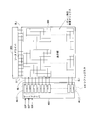
- FIG. 2 is a block diagram showing the overall configuration of the active matrix liquid crystal display device according to the first embodiment of the present invention. As shown in FIG. 2, this liquid crystal display device is common to a power supply 100, a DC / DC converter 110, a display control circuit 200, a source driver (video signal line driving circuit) 300, and a gate driver (scanning signal line driving circuit) 400. An electrode driving circuit 500 and a display unit 600 are provided. Note that the gate driver 400 is formed over a display panel including the display portion 600 using amorphous silicon, polycrystalline silicon, microcrystalline silicon, an oxide semiconductor (eg, IGZO), or the like. That is, in this embodiment, the gate driver 400 and the display unit 600 are formed on the same substrate (an array substrate that is one of the two substrates constituting the liquid crystal panel).
- the display unit 600 includes a plurality (j) of source bus lines (video signal lines) SL1 to SLj, a plurality (i) of gate bus lines (scanning signal lines) GL1 to GLi, and their source buses.
- a pixel circuit including a plurality (i ⁇ j) of pixel forming portions provided corresponding to the intersections of the lines SL1 to SLj and the gate bus lines GL1 to GLi is formed.
- the plurality of pixel forming portions are arranged in a matrix to form a pixel array.
- Each pixel forming portion includes a thin film transistor (TFT) 60 which is a switching element having a gate terminal connected to a gate bus line passing through a corresponding intersection and a source terminal connected to a source bus line passing through the intersection.
- TFT thin film transistor
- a pixel electrode connected to the drain terminal of the thin film transistor 60, a common electrode Ec which is a common electrode provided in the plurality of pixel formation portions, and a pixel provided in common in the plurality of pixel formation portions
- the liquid crystal layer is sandwiched between the electrode and the common electrode Ec.
- a pixel capacitor Cp is constituted by a liquid crystal capacitor formed by the pixel electrode and the common electrode Ec.
- an auxiliary capacitor is provided in parallel with the liquid crystal capacitor in order to reliably hold the voltage in the pixel capacitor Cp.
- the auxiliary capacitor is not directly related to the present invention, its description and illustration are omitted.
- the power supply 100 supplies a predetermined power supply voltage to the DC / DC converter 110, the display control circuit 200, and the common electrode drive circuit 500.
- the DC / DC converter 110 generates a predetermined DC voltage for operating the source driver 300 and the gate driver 400 from the power supply voltage and supplies it to the source driver 300 and the gate driver 400.
- the common electrode drive circuit 500 gives a predetermined potential Vcom to the common electrode Ec.
- the display control circuit 200 receives an image signal DAT and a timing signal group TG such as a horizontal synchronization signal and a vertical synchronization signal sent from the outside, and receives a digital video signal DV and a source start pulse for controlling image display on the display unit 600.
- a signal SSP, a source clock signal SCK, a latch strobe signal LS, a gate start pulse signal GSP, a gate end pulse signal GEP, and a gate clock signal GCK are output.
- the gate clock signal GCK is a two-phase clock signal GCK1 (hereinafter referred to as “first gate clock signal”) and GCK2 (hereinafter referred to as “second gate clock signal”) as will be described later. It consists of The gate clock signal GCK is generated from the power supply voltage, and the high-level potential is VDD and the low-level potential is VSS.
- the source driver 300 receives the digital video signal DV, the source start pulse signal SSP, the source clock signal SCK, and the latch strobe signal LS output from the display control circuit 200, and drives the video signal S for driving to the source bus lines SL1 to SLj. (1) to S (j) are applied.
- the gate driver 400 Based on the gate start pulse signal GSP, the gate end pulse signal GEP, and the gate clock signal GCK output from the display control circuit 200, the gate driver 400 generates each gate of the active scanning signals GOUT (1) to GOUT (i). The application to the bus lines GL1 to GLi is repeated with one vertical scanning period as a cycle. A detailed description of the gate driver 400 will be given later.
- the driving video signals S (1) to S (j) are applied to the source bus lines SL1 to SLj, and the scanning signals GOUT (1) to GOUT (i) are applied to the gate bus lines GL1 to GLi. Is applied, an image based on the image signal DAT sent from the outside is displayed on the display unit 600.
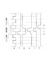
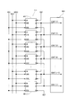
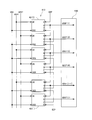
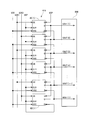
- the gate driver 400 includes a shift register 410 having a plurality of stages.
- a pixel matrix of i rows ⁇ j columns is formed, and each stage of the shift register 410 is provided so as to correspond to each row of the pixel matrix on a one-to-one basis.
- Each stage of the shift register 410 is in one of two states (first state and second state) at each time point, and a signal indicating the state (hereinafter referred to as “state signal”). It is a bistable circuit that outputs.
- the shift register 410 includes i bistable circuits 40 (1) to 40 (i).
- a high level (H level) state signal is output from the bistable circuit, and the bistable circuit is in the second state. If so, a low level (L level) state signal is output from the bistable circuit.
- a selection period a period in which a high level state signal is output from the bistable circuit and a high level scanning signal is applied to the gate bus line corresponding to the bistable circuit.
- FIG. 4 is a block diagram showing the configuration of the shift register 410 in the gate driver 400.
- the shift register 410 includes i bistable circuits 40 (1) to 40 (i).
- Each bistable circuit includes an input terminal for receiving a clock signal CK (hereinafter referred to as “first clock”) and a low-level DC power supply potential VSS (the magnitude of this potential is also referred to as “VSS potential”). )), An input terminal for receiving the set signal S, an input terminal for receiving the reset signal R, and an output terminal for outputting the status signal Q.
- first clock hereinafter referred to as “first clock”
- VSS low-level DC power supply potential
- the shift register 410 is supplied with the first gate clock signal GCK1 and the second gate clock signal GCK2 which are two-phase clock signals as the gate clock signal GCK. As shown in FIG. 5, the first gate clock signal GCK1 and the second gate clock signal GCK2 are out of phase with each other by one horizontal scanning period, and both are high level only for one horizontal scanning period in the two horizontal scanning periods. The state becomes (H level).
- each bistable circuit of the shift register 410 is as follows.
- the first gate clock signal GCK1 is given as the first clock CK.
- the second gate clock signal GCK2 is given as the first clock CK.
- the gate start pulse signal GSP is given as the set signal S to the first stage 40 (1).
- the state signal Q of the previous stage is given as the set signal S.
- the gate end pulse signal GEP is given as the reset signal R to the i-th stage 40 (i).
- the status signal Q of the next stage is given as the reset signal R.
- the low-level DC power supply potential VSS is commonly applied to all bistable circuits.
- the gate start pulse signal GSP as the set signal S is given to the first stage 40 (1) of the shift register 410, based on the first gate clock signal GCK1 and the second gate clock signal GCK2.
- the pulses included in the gate start pulse signal GSP (this pulse is included in the status signal Q output from each stage) are sequentially transferred from the first stage 40 (1) to the i-th stage 40 (i). .
- the status signals Q output from the respective stages 40 (1) to 40 (i) are sequentially set to the high level.
- the state signal Q output from each of the stages 40 (1) to 40 (i) is applied to the gate bus lines GL1 to GLi as scanning signals GOUT (1) to GOUT (i).
- a scanning signal that sequentially becomes high level (active) for each horizontal scanning period is given to the gate bus line in the display unit 600.
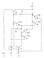
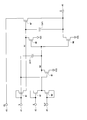
- FIG. 1 is a circuit diagram showing a configuration of the bistable circuit (configuration of one stage of the shift register 410) in the present embodiment.
- the bistable circuit includes six thin film transistors M1 to M3 and M5 to M7, and two capacitors CAP1 and CAP2.
- the bistable circuit has three input terminals 41 to 43 and one output terminal 48 in addition to the input terminal for the low-level DC power supply potential VSS.
- the input terminal that receives the set signal S is denoted by reference numeral 41
- the input terminal that receives the reset signal R is denoted by reference numeral 42
- the input terminal that receives the first clock CK is denoted by reference numeral 43.
- the output terminal for outputting the status signal Q is denoted by reference numeral 48.
- the source terminal of the thin film transistor M1, the gate terminal of the thin film transistor M2, the drain terminal of the thin film transistor M5, and one end of the capacitor CAP1 are connected to each other.
- a region (wiring) in which these are connected to each other is referred to as a “first node” for convenience.
- the drain terminal of the thin film transistor M3, the gate terminal of the thin film transistor M5, the gate terminal of the thin film transistor M6, the source terminal of the thin film transistor T7, and one end of the capacitor CAP2 are connected to each other.
- a region (wiring) in which these are connected to each other is referred to as a “second node” for convenience.
- the first node is denoted by reference numeral N1
- the second node is denoted by reference numeral N2.
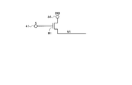
- the gate terminal and the drain terminal are connected to the input terminal 41 (that is, diode connection), and the source terminal is connected to the first node N1.
- the gate terminal is connected to the first node N1
- the drain terminal is connected to the input terminal 43
- the source terminal is connected to the output terminal 48.
- the gate terminal is connected to the input terminal 41
- the drain terminal is connected to the second node N2
- the source terminal is connected to the input terminal for the DC power supply potential VSS.
- the gate terminal is connected to the second node N2
- the drain terminal is connected to the first node N1
- the source terminal is connected to the input terminal for the DC power supply potential VSS.
- the gate terminal is connected to the second node N2
- the drain terminal is connected to the output terminal 48
- the source terminal is connected to the input terminal for the DC power supply potential VSS.
- the gate terminal and the drain terminal are connected to the input terminal 42 (that is, diode connection), and the source terminal is connected to the second node N2.
- the capacitor CAP1 has one end connected to the first node N1 and the other end connected to the output terminal 48.
- the capacitor CAP2 has one end connected to the second node N2 and the other end connected to the input terminal 41.
- the capacitance value C2 of the capacitor CAP2 preferably satisfies the following formula (1).
- the capacitance value C2 of the capacitor CAP2 is It is preferable to satisfy the formula (2).
- the thin film transistor M1 changes the potential of the first node N1 toward the high level when the set signal S is at the high level.
- the thin film transistor M2 applies the potential of the first clock CK to the output terminal 48 when the potential of the first node N1 is at a high level.
- the thin film transistor M3 changes the potential of the second node N2 toward the VSS potential when the set signal S is at a high level.
- the thin film transistor M5 changes the potential of the first node N1 toward the VSS potential when the potential of the second node N2 is at a high level.
- the thin film transistor M6 changes the potential of the output terminal 48 toward the VSS potential when the potential of the second node N2 is at a high level.
- the thin film transistor M7 changes the potential of the second node N2 toward the high level when the reset signal R is at the high level.
- the capacitor CAP1 functions as a compensation capacitor for maintaining the potential of the first node N1 at a high level during the period when the gate bus line connected to the bistable circuit is in a selected state.
- the capacitor CAP2 functions to stabilize the circuit operation by lowering the potential of the second node N2 when the gate bus line connected to the bistable circuit is selected.
- the first node turn-on switching element is realized by the thin film transistor M1
- the first output control switching element is realized by the thin film transistor M2
- the first second node turn-off switching element is realized by the thin film transistor M3.
- the first first node turn-off switching element is realized by the thin film transistor M6, and the first second node turn-on is realized by the thin film transistor M7.
- a switching element is realized.
- the input terminal 41 implements a first input node
- the input terminal 42 implements a second input node
- the output terminal 48 implements a first output node.
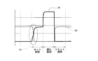
- the period from time t1 to time t2 corresponds to the selection period.
- one horizontal scanning period immediately before the selection period is referred to as “set period”
- one horizontal scanning period immediately after the selection period is referred to as “reset period”.
- a period other than the selection period, the set period, and the reset period is referred to as a “normal operation period”.
- the potential of the second node N2 is maintained at a high level. Therefore, the thin film transistors M5 and M6 are in an on state. Since parasitic capacitance exists between the gate and drain of the thin film transistor M2, noise is generated at the first node N1 due to fluctuations in the waveform of the first clock CK (see FIG. 6), but the thin film transistor M5 is turned on. Therefore, the potential of the first node N1 is pulled to a low level.
- the state signal Q (output terminal 48) due to noise generated in the first node N1 and fluctuations in the video signal voltage
- the state signal Q since the thin film transistor M6 is in the on state, the state signal Q Is pulled to a low level. As described above, during this period, the potential of the first node N1 and the potential of the state signal Q are maintained at a low level.
- the set signal S changes from low level to high level. Since the thin film transistor M1 is diode-connected as shown in FIG. 1, when the set signal S goes high, the thin film transistor M1 is turned on, and the capacitor CAP1 is charged (here, precharged). As a result, the potential of the first node N1 changes from the low level to the high level, and the thin film transistor M2 is turned on. However, since the first clock CK is at a low level during the set period, the potential of the state signal Q is maintained at a low level. Further, when the set signal S becomes high level, the thin film transistor M3 is turned on, and the potential of the second node N2 becomes low level.
- the thin film transistors M5 and M6 are turned off.
- the set signal S becomes high level, and the potential of the second node N2 becomes low level, so that the capacitor CAP2 is charged based on the potential difference between the input terminal 41 and the second node N2.
- the set signal S changes from high level to low level.
- the thin film transistor M5 is in an off state.
- the first node N1 is in a floating state.
- the first clock CK changes from the low level to the high level.
- the potential of the first node N1 also increases as the potential of the input terminal 43 increases (the first node N1 is bootstrapped). .
- the thin film transistor M2 is completely turned on, and the potential of the state signal Q rises to a level sufficient for the gate bus line connected to the output terminal 48 of the bistable circuit to be selected.
- the potential of the second node N2 tends to increase as the potential of the first node N1 and the potential of the state signal Q increase.
- the capacitor CAP2 is charged based on the potential difference between the input terminal 41 and the second node N2 during the set period, and the set signal S changes from the high level to the low level during this period, so that the second The potential of the node N2 is maintained at a low level.
- the first clock CK changes from high level to low level. Since the thin film transistor M2 is in the on state at the time point t2, the potential of the state signal Q decreases as the potential of the input terminal 43 decreases. As the potential of the state signal Q decreases in this way, the potential of the first node N1 also decreases via the capacitor CAP1. During this period, the reset signal R changes from the low level to the high level. For this reason, the thin film transistor M7 is turned on, and the potential of the second node N2 is at a high level. Thereby, the thin film transistors M5 and M6 are turned on. As a result, during the reset period, the potential of the first node N1 and the potential of the state signal Q are lowered to a low level.
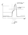
- FIG. 7 is a signal waveform diagram showing changes in potentials of the first node N1 and the second node N2 in the present embodiment.
- FIG. 8 is a signal waveform diagram showing changes in potentials of first node N1 and second node N2 in the conventional configuration shown in FIG.
- FIG. 9 is a signal waveform diagram showing changes in potentials of first node N1 and second node N2 in the conventional configuration shown in FIG.
- the potential of the second node N2 decreases due to the increase of the potential of the first node N1
- the potential of the second node N2 is decreased in the following order.
- the set signal Gn ⁇ 1 changes from the low level to the high level
- the potential of the first node N1 rises.
- the transistor group TG1 is turned on based on the increase in the potential of the first node N1, thereby decreasing the potential of the second node N2.
- the potential of the second node N2 is decreased after the potential of the first node N1 is increased. Incidentally, as shown in FIG.
- the bistable circuit is provided with a transistor TR4 for decreasing the potential of the first node N1 based on the potential of the second node N2. For this reason, in the period immediately after the start of the set period, the potential of the first node N1 tends to decrease based on the potential of the second node N2 while increasing based on the set signal Gn-1. As a result, the potential at the first node N1 during the set period does not rise rapidly, as can be understood from the waveform of the portion indicated by reference numeral 73 in FIG. Therefore, the circuit operation lacks stability.
- the potential of the second node N2 directly decreases as the potential of the set signal S changes from the low level to the high level. Since the thin film transistor M5 is turned off when the potential of the second node N2 decreases, the increase in the potential of the first node N1 during the set period is not hindered. As a result, the potential at the first node N1 rises rapidly in the set period, as can be seen from the waveform of the portion denoted by reference numeral 71 in FIG. Therefore, the stability of the circuit operation is improved as compared with the conventional configuration.
- the potential of the second node N2 for decreasing the potential of the first node is decreased by increasing the potential of the first node N1”. Is not employed, the occurrence of large noise at the first node N1 is suppressed. Further, the capacitor CAP2 is charged during the set period, and the set signal S changes from the high level to the low level during the selection period, so that the potential of the second node N2 is maintained at the low level during the selection period. . For this reason, it is suppressed that the electric potential of the 1st node N1 falls during a set period, and stability of circuit operation is ensured.
- the second node N2 after the potential of the second node N2 rises based on the rise of the potential of the set signal Gn-1, the second node N2 is in a floating state during the selection period.
- the potential of the second node N2 rises due to the presence of parasitic capacitance between the gate and drain of the transistors TG3 and TR4. Therefore, the transistors TG3 and TR4 are slightly turned on during the selection period.
- an increase in the potential of the gate signal Gn (corresponding to the state signal Q in the present embodiment) is prevented, and the potential of the first node N1 that should be maintained at a high level is as shown by a portion 74 in FIG. To drop.
- the potential of the first node N1 is maintained at a sufficiently high level during the selection period as indicated by reference numeral 72 in FIG.
- the relationship between the capacitance values of the thin film transistors M3, M5, and M6 and the capacitance value of the capacitor CAP2 satisfies the above equation (1) so that the increase in the potential of the second node N2 during the selection period is surely suppressed. Is preferred. Further, current leakage may occur in the thin film transistors M3 and M7 due to the influence of noise generated in the set signal S and the reset signal R, and the potential of the second node N2 may be reduced. However, according to the present embodiment, the capacitor CAP2 is charged. By accumulating, a decrease in the potential of the second node N2 due to such current leakage is suppressed.
- the capacitor CAP2 has a function equivalent to that of the frame capacitor Ccharge in the configuration shown in FIGS. For this reason, a shift register excellent in operational stability is realized without increasing the number of necessary circuit elements as compared with the conventional configuration.
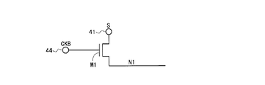
- the gate terminal and the drain terminal are connected to the input terminal 41, and the source terminal is connected to the first node N1.
- the present invention is not limited to this.
- the gate terminal is connected to the input terminal 41, and the drain terminal is an input terminal 44 (hereinafter also referred to as “second clock”) for receiving a clock signal CKB (hereinafter also referred to as the second clock CKB).
- the thin film transistor M1 may be configured such that the input terminal for receiving is connected to the reference numeral 44) and the source terminal is connected to the first node N1 (first modification).
- the shift register 411 is configured so that the first clock CK and the second clock CKB, which are alternately at a high level every one horizontal scanning period, are supplied to the bistable circuit as shown in FIG. 12 is configured. That is, in the first modification, for the odd-numbered stages of the shift register 411, the first gate clock signal GCK1 is supplied as the first clock CK, and the second gate clock signal GCK2 is supplied as the second clock CKB. For the even stages of the shift register 411, the second gate clock signal GCK2 is supplied as the first clock CK, and the first gate clock signal GCK1 is supplied as the second clock CKB.
- the second clock CKB is applied to the drain terminal of the thin film transistor M1.
- each bistable circuit is supplied with the first gate clock signal GCK1 or the second gate clock signal GCK2 as the second clock CKB.
- the first gate clock signal GCK1 and the second gate clock are supplied.
- the signal GCK2 is generated from the power supply voltage. Therefore, in the first modification, the power supply voltage is a charge supply source of the first node N1. For this reason, unlike the first embodiment, the flow of charge from the input terminal 41 to the first node N1 is suppressed, and the potential of the input terminal 41 rises quickly. Note that even if the drain terminal of the thin film transistor M1 is connected to an input terminal for receiving a high-level DC power supply potential VDD (the magnitude of this potential is also referred to as “VDD potential”), FIG. The same effect as that shown in FIG.
- the thin film transistor M1 is configured such that the gate terminal is connected to the input terminal 44, the drain terminal is connected to the input terminal 41, and the source terminal is connected to the first node N1. (2nd modification) is also good. According to the second modification, the thin film transistor M1 is turned on based on the power supply voltage. For this reason, the thin film transistor M1 is quickly turned on during the set period, and the potential of the first node N1 rises quickly.
- the gate terminal and the drain terminal are connected to the input terminal 42, and the source terminal is connected to the second node N2.
- the present invention is not limited to this.
- the thin film transistor M7 may be configured such that the gate terminal is connected to the input terminal 42, the drain terminal is connected to the input terminal 44, and the source terminal is connected to the second node N2. (Third modification).
- the second clock CKB is applied to the drain terminal of the thin film transistor M7, the power supply voltage becomes a charge supply source of the second node N2.
- the thin film transistor M7 may be configured such that the gate terminal and the drain terminal are connected to the input terminal 44, and the source terminal is connected to the second node N2 (fourth modification). Example). Further, as shown in FIG. 16, the gate terminal is connected to the input terminal 44, the drain terminal is connected to the input terminal for the high-level DC power supply potential VDD, and the source terminal is connected to the second node N2.
- the thin film transistor M7 may be configured (fifth modification). In the configuration shown in FIG. 1 (configuration in the first embodiment), the thin film transistor M7 is turned on only once during one vertical scanning period, but according to the fourth and fifth modified examples.
- the thin film transistor M7 Since the thin film transistor M7 is turned on every two horizontal scanning periods, electric charges are supplied to the second node N2 in a short cycle. For this reason, the potential of the second node N2 is reliably maintained at a high level during the normal operation period. Incidentally, since the set signal S and the second clock CKB are at a high level during the set period (see the period from time t0 to time t1 in FIG. 11), the thin film transistor M3 and the thin film transistor M7 are turned on at almost the same timing. There is a concern that the circuit operation becomes unstable due to the state. Therefore, it is preferable that the transistor size (channel width / channel length) of the thin film transistor M7 be sufficiently smaller than the transistor size of the thin film transistor M3.
- the driving force of the thin film transistor M7 becomes smaller than the driving force of the thin film transistor M3, and even if the thin film transistor M3 and the thin film transistor M7 are turned on at substantially the same timing during the set period, the potential of the second node N2 decreases. It is suppressed that operation becomes unstable.
- the shift register 411 is configured as shown in FIG.
- the gate terminal is connected to the input terminal 41, the drain terminal is connected to the second node N2, and the source terminal is connected to the input terminal for the DC power supply potential VSS.
- the present invention is not limited to this.
- the source terminal of the thin film transistor M3 may be connected to the output terminal 48 (sixth modification).
- the source terminal of the thin film transistor M3 may be connected to the input terminal 43 (seventh modified example). The reason for this is as follows.
- the potential of the second node N2 should be maintained at a low level. Further, as can be seen from FIG. 6, during the set period, the potential of the output terminal 48 (the potential of the state signal Q) and the potential of the input terminal 43 (the potential of the first clock CK) are at a low level. As described above, regarding the thin film transistor M3 in which the set signal S is given to the gate terminal and the second node N2 is connected to the drain terminal, even if the source terminal is connected to the output terminal 48 or the input terminal 43, The potential of the second node N2 is at a low level.
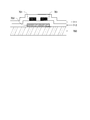
- FIG. 19 is a partial cross-sectional view of an array substrate on which a gate driver 400, a pixel circuit, and the like are formed.
- the array substrate has a laminated structure for forming a gate driver 400, a pixel circuit, and the like, and two metal films (metal layers) are included in the laminated structure.
- a metal film 702, a protective film 712, a metal film 701, and a protective film 711 are stacked on a glass substrate 700.
- the metal film 701 is used for forming a source electrode (and a drain electrode) of a thin film transistor provided in the gate driver 400 or the pixel circuit. Therefore, hereinafter, such a metal film 701 is referred to as “source metal” 701.
- the metal film 702 is used for forming a gate electrode of a thin film transistor. Therefore, hereinafter, such a metal film 702 is referred to as “gate metal” 702. Note that the source metal 701 and the gate metal 702 are not only used as electrodes of the thin film transistor but also used as a wiring pattern formed in the gate driver 400 or the pixel circuit.
- the capacitor CAP2 has one end connected to the second node N2 and the other end connected to the input terminal 41.
- the electrode on one end side is preferably formed of a source metal 701
- the electrode on the other end side is preferably formed of a gate metal 702.
- the capacitor CAP2 and the thin film transistor M3 are arranged adjacent to each other.
- the drain electrode is formed of the source metal 701
- the gate electrode is formed of the gate metal 702.
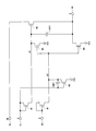
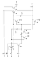
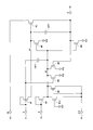
- FIG. 21 is a circuit diagram showing a configuration of a bistable circuit according to the second embodiment of the present invention.
- the overall configuration and operation of the liquid crystal display device and the configuration and operation of the gate driver are the same as those in the first embodiment, and a description thereof will be omitted.
- the thin film transistor M5 has a gate terminal connected to the second node N2, a drain terminal connected to the first node N1, and a source terminal connected to the input terminal for the DC power supply potential VSS. It was. However, the present invention is not limited to this. As shown in FIG. 21, the source terminal of the thin film transistor M ⁇ b> 5 may be connected to the output terminal 48.
- the potential of the state signal Q is applied to the source terminal of the thin film transistor M5.
- the potential of the first node N1 connected to the drain terminal of the thin film transistor M5 is at a high level, and the state signal Q is also at a high level (see FIG. 6). Therefore, the voltage between the drain and the source of the thin film transistor M5 in the selection period is reduced as compared with the first embodiment in which the DC power supply potential VSS is applied to the source terminal of the thin film transistor M5.
- the potential of the first node N1 is reliably maintained at a high level during the selection period, and the stability of the circuit operation is effectively enhanced.
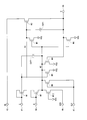
- FIG. 22 is a circuit diagram showing a configuration of a bistable circuit according to the third embodiment of the present invention.
- the overall configuration and operation of the liquid crystal display device and the configuration and operation of the gate driver are the same as those in the first embodiment, and a description thereof will be omitted.
- the bistable circuit is provided with a thin film transistor M4 in addition to the components in the first embodiment shown in FIG.
- the gate terminal is connected to the output terminal 48
- the drain terminal is connected to the second node N2
- the source terminal is connected to the input terminal for the DC power supply potential VSS.
- the thin film transistor M4 functions to change the potential of the second node N2 toward the VSS potential when the potential of the output terminal 48 is at a high level.
- the thin film transistor M4 realizes a second second node turn-off switching element.
- the gate terminal of the thin film transistor M4 is connected to the output terminal 48. Further, during the selection period, the potential of the state signal Q (the potential of the output terminal 48) is at a high level. As described above, the thin film transistor M4 is turned on in the selection period. Thereby, during the selection period, the potential of the second node N2 is pulled to a low level. Therefore, according to the present embodiment, the potential of the second node N2 is reliably maintained at a low level during the selection period, and the stability of the circuit operation is effectively enhanced.
- FIG. 23 is a circuit diagram showing a configuration of a bistable circuit according to the fourth embodiment of the present invention.
- the overall configuration and operation of the liquid crystal display device and the configuration and operation of the gate driver are the same as those in the first embodiment, and a description thereof will be omitted.
- the bistable circuit is provided with a thin film transistor M10 in addition to the components in the third embodiment shown in FIG.
- the gate terminal is connected to the input terminal 42
- the drain terminal is connected to the output terminal 48
- the source terminal is connected to the input terminal for the DC power supply potential VSS.
- the thin film transistor M10 functions to change the potential of the state signal Q toward the VSS potential when the reset signal R is at a high level.
- the thin film transistor M10 implements a second first output node turn-off switching element. Note that the thin film transistor M10 may be provided in addition to the components in the first embodiment shown in FIG.
- the reset signal R changes from the low level to the high level and the thin film transistor M7 is turned on, so that the potential of the second node N2 changes from the low level. It was changing to a high level. Then, the potential of the second node N2 is changed from the low level to the high level and the thin film transistor M6 is turned on, so that the potential of the state signal Q is lowered.
- the thin film transistor M10 is turned on when the reset signal R changes from the low level to the high level. For this reason, when the reset signal R changes from the low level to the high level, the potential of the state signal Q directly decreases.
- FIG. 24 is a diagram illustrating a simulation result of a change in the potential of the state signal Q.
- the potential of the state signal Q is rapidly reduced during the reset period as compared to the configuration without the thin film transistor M10.
- FIG. 25 is a circuit diagram showing a configuration of a bistable circuit in a modification of the fourth embodiment.
- the bistable circuit is provided with a thin film transistor M11 in addition to the components shown in FIG.
- the gate terminal is connected to the input terminal 42
- the drain terminal is connected to the first node N1
- the source terminal is connected to the input terminal for the DC power supply potential VSS.
- the thin film transistor M11 functions to change the potential of the first node N1 toward the VSS potential when the reset signal R is at a high level.
- the thin film transistor M11 realizes a second first node turn-off switching element.
- the reset signal R changes from the low level to the high level and the thin film transistor M7 is turned on, so that the potential of the second node N2 changes from the low level. It was changing to a high level. Then, the potential of the second node N2 is changed from the low level to the high level and the thin film transistor M5 is turned on, so that the potential of the first node N1 is lowered to the low level.
- the thin film transistor M11 is turned on when the reset signal R changes from the low level to the high level. For this reason, when the reset signal R changes from the low level to the high level, the potential of the first node N1 directly decreases toward the VSS potential.
- the two thin film transistors M5 and M11 function so that the potential of the first node N1 decreases during the reset period. For this reason, even when the circuit is operated at high speed, the potential of the first node N1 can be reliably lowered to a low level during the reset period. This improves the stability of the circuit operation when the load capacity of the gate bus line is large.
- FIG. 26 is a circuit diagram showing a configuration of a bistable circuit according to the fifth embodiment of the present invention.
- the overall configuration and operation of the liquid crystal display device and the configuration and operation of the gate driver are the same as those in the first embodiment, and a description thereof will be omitted.
- the first node N1 is precharged based on the change of the set signal S from the low level to the high level during the set period.
- the high-level potential with respect to the first clock CK is the VDD potential and the low-level potential is the VSS potential
- the potential Vn of the first node N1 immediately before the end of the set period is theoretically expressed by the following formula ( It becomes the value shown in 3).
- Vth is a threshold voltage of the thin film transistor M1.
- Vn VDD ⁇ Vth (3)
- the first clock CK changes from the low level to the high level.
- the potential of the first node N1 increases as the potential of the input terminal 43 increases.
- Vn 2 ⁇ VDD ⁇ Vth (4)
- the first node N1 when a thin film transistor using a semiconductor layer having a high mobility such as microcrystalline silicon ( ⁇ c-Si) or an oxide semiconductor (for example, IGZO) is employed, the first node N1 as shown in the above equation (4).
- the gate bus line can be driven sufficiently without increasing the potential of the gate bus line.
- the potential of the first node N1 is inevitably increased based on the parasitic capacitance between the gate and the drain of the thin film transistor M2. Therefore, in the present embodiment, as shown in FIG. 26, the thin film transistor M1 for increasing the potential of the first node N1 based on the set signal S has a multi-gate configuration.
- Vn VDD ⁇ n * Vth (5)
- the potential of the first node N1 immediately after the precharge in the set period is compared with the first to fourth embodiments. Become lower. Therefore, when this embodiment is compared with the first to fourth embodiments, the potential of the first node N1 immediately before the end of the selection period is higher in the present embodiment than in the first to fourth embodiments. Becomes lower. As a result, the voltage applied to the gate terminal of the thin film transistor M2 is reduced, and the gate insulating film breakdown of the thin film transistor M2 is suppressed.
- a thin film transistor using an oxide semiconductor (for example, IGZO) as a semiconductor layer has a relatively low breakdown voltage. Therefore, by adopting the configuration in this embodiment, the gate insulating film breakdown of the thin film transistor M2 is effectively suppressed. .
- FIG. 27 is a diagram illustrating a simulation result of a change in the potential of the first node N1.
- the increase in the potential of the first node N1 in the set period is smaller than in the configuration in which the thin film transistor M1 is not multi-gate.
- the potential of the first node N1 immediately before the end of the selection period is lower than in the configuration in which the thin film transistor M1 is not multi-gate.
- the gate insulating film of the thin film transistor is destroyed. Can be suppressed, and the stability of the circuit operation can be improved.
- FIG. 28 is a circuit diagram showing a configuration of a bistable circuit in a modified example of the fifth embodiment.
- the thin film transistor M5 is multi-gated.
- a thin film transistor having a large leakage current when a high voltage is applied between the drain and the source (a leakage current when the gate-source voltage is 0 V) is employed. If so, there is a concern that the potential of the first node N1 decreases during the selection period. The reason for this is as follows. As can be understood from FIGS. 1 and 6, the drain-source voltages of the thin film transistors M1 and M5 increase during the selection period. In the selection period, the potential of the set signal S and the potential of the second node N2 are at a low level. For this reason, current leakage occurs in the thin film transistors M1 and M5 during the selection period, and the potential of the first node N1 decreases.
- the potential of the state signal Q may not increase to the high level potential of the first clock CK. Further, during the reset period, the potential of the state signal Q decreases due to the charge flowing through the thin film transistor M2 from the output terminal 48 side to the input terminal 43 side, so that the first node connected to the gate terminal of the thin film transistor M2 If the potential of N1 is low, the time required for the potential of the state signal Q to fall to the low level becomes long. Therefore, in the present modification, as shown in FIG. 28, the thin film transistors M1 and M5 having the drain terminal or the source terminal connected to the first node N1 are multi-gated.
- the off currents of the thin film transistors M1 and M5 are relatively small. For this reason, for example, even when a thin film transistor using microcrystalline silicon ( ⁇ c-Si) as a semiconductor layer, that is, a thin film transistor with a large leakage current is employed, the potential of the state signal Q can be sufficiently increased during the selection period. In addition, the potential of the state signal Q can be quickly lowered during the reset period.
- ⁇ c-Si microcrystalline silicon
- the thin film transistor M11 may be multi-gate as shown in FIG. 25
- FIG. 30 is a circuit diagram showing a configuration of a bistable circuit according to the sixth embodiment of the present invention.
- the bistable circuit is provided with a thin film transistor M9 and an output terminal 49 in addition to the components in the third embodiment shown in FIG.
- a second output control switching element is realized by the thin film transistor M9, and a second output node is realized by the output terminal 49.
- a signal output from the output terminal 49 of each bistable circuit is a signal (hereinafter referred to as “another stage control signal”) Z for controlling the operation of the bistable circuit in a stage different from each bistable circuit.
- the bistable circuit of the different stage is given.
- the shift register 412 is configured as shown in FIG. That is, the other stage control signal Z output from the output terminal 49 of each stage of the shift register 412 is given to the previous stage as the reset signal R and to the next stage as the set signal S.
- the state signal Q output from the output terminal 48 of each stage of the shift register 412 is used only as a signal for driving the gate bus line connected to the output terminal 48.
- the signal for driving the gate bus line corresponding to each stage differs from the signal for controlling the operation of the previous stage and the next stage of each stage. Signal. Therefore, the rounding of the waveform of the set signal S and the reset signal R can be reduced in each bistable circuit. Thereby, even when the load capacity of the gate bus line is large, the operation based on the set signal S and the operation based on the reset signal R are promptly performed in each bistable circuit, and the stability of the circuit operation is improved.
- FIG. 32 is a block diagram showing the configuration of the shift register 413 in the gate driver 400 in the first modification of the sixth embodiment.
- the other stage control signal Z output from the bistable circuit is not given to the next stage as the set signal S. That is, in the present modification, the other stage control signal Z output from the bistable circuit is used only as the reset signal R. For this reason, the status signal Q output from the bistable circuit is used as a signal for driving the gate bus line, and also used as a set signal S for controlling the operation of the next stage.
- the set period it is sufficient that the potential of the first node N1 rises to a sufficient level by the end of the set period.
- the potential of the state signal Q should be lowered to a low level immediately after the start of the reset period. Considering these things, it is considered that it is not preferable to cause waveform rounding in the reset signal R rather than waveform rounding in the set signal S in terms of circuit operation. Therefore, by adopting a configuration in which the other-stage control signal Z is used only as the reset signal R as in the present modification, the load applied to the output terminal 49 is reduced as compared with the sixth embodiment, and the shift register 413 is used. The rise time of the reset signal R in each stage is shortened. As a result, the potential of the state signal Q quickly decreases to a low level after the selection period ends, and the reliability of the circuit operation is improved.
- FIG. 33 is a circuit diagram showing a configuration of a bistable circuit according to a second modification of the sixth embodiment.
- the drain terminal of the thin film transistor M7 is connected to the input terminal 44 for receiving the second clock CKB.
- the shift register 414 is configured so that the bistable circuit is supplied with the first clock CK and the second clock CKB that alternately become high for each horizontal scanning period as shown in FIG. 34 is configured.
- the second clock CKB is applied to the drain terminal of the thin film transistor M7, the power supply voltage becomes the charge supply source of the second node N2. Further, the load applied to the input terminal 42 is reduced. Therefore, compared with the sixth embodiment, the flow of charge from the input terminal 42 to the second node N2 is suppressed, and the potential of the input terminal 42 rises quickly.
- the rising timing of the reset signal R and the rising timing of the second clock CKB are substantially the same, but the reset signal is higher than the second clock CKB. It takes more time for R to stand up completely. The same applies to the fall of those signals. This is because the state signal Q output from the bistable circuit is used not only as the reset signal R of the previous stage but also as the scanning signal for driving the gate bus line and the set signal S of the next stage. This is because the load on the line is large. Therefore, the reset signal R is more likely to be rounded than the second clock CKB. Therefore, in the period after time t3 in FIG.
- the potential of the gate terminal of the thin film transistor M7 may become higher than the VSS potential after the potential of the drain terminal of the thin film transistor M7 has dropped to the VSS potential.
- the signal used as the reset signal R is different from the signal used as the scanning signal and the set signal S.
- the other stage control signal Z output from the output terminal 49 of each stage of the shift register 414 is used as the reset signal R of the preceding stage of each stage, and is output from the output terminal 48 of each stage of the shift register 414.
- the status signal Q is used as a scanning signal for driving a gate bus line corresponding to each stage and a set signal S for the next stage of each stage.
- FIG. 35 is a circuit diagram showing a configuration of a bistable circuit according to a third modification of the sixth embodiment.
- the drain terminal of the thin film transistor M2 is connected to the input terminal for the high-level DC power supply potential VDD.
- the bistable circuit operates as follows during the set period and the selection period (see FIG. 36).
- the set signal S changes from low level to high level.
- the thin film transistor M1 is turned on, and the capacitor CAP1 is charged (precharged here). Therefore, the potential of the first node N1 changes from the low level to the high level, and the thin film transistors M2 and M9 are turned on. Since the VDD potential is applied to the drain terminal of the thin film transistor M2, the potential of the state signal Q rises when the thin film transistor M2 is turned on. The potential of the other-stage control signal Z is maintained at the low level because the first clock CK is at the low level during the set period. Further, when the set signal S becomes high level, the thin film transistor M3 is turned on, and the potential of the second node N2 becomes low level.
- the set signal S changes from high level to low level.
- the first node N1 is in a floating state.
- the first clock CK changes from the low level to the high level.
- the thin film transistors M2 and M9 are completely turned on.
- the potential of the state signal Q rises to the VDD potential.
- the potential of the other stage control signal Z rises to the high level potential of the first clock CK. Note that the potential of the second node N2 is maintained at a low level as in the first embodiment.
- the rise of the potential of the state signal Q is started in the set period. For this reason, the gate bus line is quickly selected during the selection period, and a sufficient charging time for the pixel capacitance is ensured.
- the drain potential of the thin film transistor M2 is supplied with the VDD potential instead of the clock signal, the load on the clock signal wiring is reduced. For this reason, the occurrence of waveform rounding for the clock signal is suppressed, and the power consumption is reduced.
- the voltage source for scanning signals and the voltage source for circuit driving are different systems.
- the relationship between the potential VCK on the high level side of the clock signal and the potential on the high level side of the scanning signal (potential for turning on the thin film transistor whose gate terminal is connected to the gate bus line for transmitting the scanning signal) is VGH. It is preferable that the following formula (6) and the following formula (7) are satisfied. VCK ⁇ VGH / 2 (6) VCK ⁇ VGH (7)
- the reason why it is preferable to satisfy the above formula (6) is as follows.
- the potential of the scanning signal In the selection period, the potential of the scanning signal must be sufficiently increased so that the thin film transistor 60 (see FIG. 2) of each pixel formation portion in the display portion 600 is turned on. For this reason, the potential of the first node N1 must be greater than or equal to the VGH during the selection period.
- the potential of the first node N1 is ideally twice as large as VCK. For this reason, when VCK is made smaller than half of VGH, the potential of the first node N1 does not become VGH or higher during the selection period. As a result, the potential of the scanning signal for driving each gate bus line cannot be sufficiently increased during the selection period.
- the reason why it is preferable to satisfy the above formula (7) is as follows.
- power consumption W by an electric signal is proportional to the product of the square of voltage (amplitude) V, capacitance C, and frequency f.
- the frequency f of the clock signal is relatively large and the power consumption W is proportional to the square of the voltage V, the voltage V of the clock signal, that is, the potential VCK on the high level side of the clock signal is lowered. By doing so, the power consumption W is greatly reduced. Therefore, it is preferable that the above formula (7) is established.
- the clock signal is no longer applied to the thin film transistor M2 having a relatively large parasitic capacitance. Therefore, even when the above equation (7) is not established, the magnitude of the power consumption W by the clock signal is affected. The size of the exerted capacitance C is reduced, and the effect of reducing power consumption can be obtained.
- FIG. 37 is a circuit diagram showing a configuration of a bistable circuit according to the seventh embodiment of the present invention.
- the bistable circuit is provided with a thin film transistor M8 in addition to the components in the first embodiment shown in FIG.
- the thin film transistor M8 realizes a second second node turn-on switching element.
- the gate terminal and the drain terminal are connected to the input terminal 45 for receiving the clear signal CLR for initializing each bistable circuit, and the source terminal is connected to the second node N2. Note that a third input node is realized by the input terminal 45.
- the thin film transistor M8 functions to change the potential of the second node N2 toward the high level when the clear signal CLR is at the high level.
- the shift register 415 is configured as shown in FIG. 38 so that the clear signal CLR is given to each bistable circuit.
- the clear signal CLR is set to a high level only during a part of the period after the power-on of the device before the first pulse of the gate start pulse signal GSP is generated. During this period, the level is low.
- the change timing of the clear signal CLR and the change timing of the first clock CK are synchronized, but they may not be synchronized.
- the second node N2 is charged only by the reset signal R. For this reason, after the device is turned on, in each bistable circuit, the potential of the second node N2 is indefinite during the period until the reset signal R first becomes high level. For example, if the potential of the second node N2 after the device is turned on is the VSS potential, the thin film transistors M5 and M6 are turned off during the period when the first image is displayed. For this reason, when noise occurs in the first node N1 due to the presence of the parasitic capacitance between the gate and the drain of the thin film transistor M2, the potential of the state signal Q that should originally be maintained at the low level is maintained at the low level. Disappear.
- the clear signal CLR is at a high level during the period from when the device is turned on until the operation of the shift register 415 starts. Since the thin film transistor M8 is diode-connected as shown in FIG. 37, when the clear signal CLR becomes a high level, the thin film transistor M8 is turned on, and the potential of the second node N2 changes from an indefinite state to a high level. . Therefore, the thin film transistors M5 and M6 are turned on before the operation of the shift register 415 is started. Thereby, at the start of the operation of the shift register 415, the potential of the first node N1 and the potential of the state signal Q are low in all bistable circuits, and the stability of the circuit operation is improved.
- the gate end pulse signal GEP may be used as the clear signal CLR. Thereby, the stability of the circuit operation is further improved while reducing the number of signals. Furthermore, when the gate end pulse signal GEP is used as the clear signal CLR, it is preferable to start the shift register in response to the oscillation of the gate end pulse signal GEP as shown in FIG.
- FIG. 42 is a circuit diagram showing a configuration of a bistable circuit in the first modification example of the seventh embodiment.
- a thin film transistor M12 is provided in addition to the components in the seventh embodiment shown in FIG.
- the thin film transistor M12 realizes a second node level lowering switching element.
- the gate terminal is connected to the input terminal for the low-level DC power supply potential VSS
- the drain terminal is connected to the second node N2
- the source terminal has a potential lower than the VSS potential at the second node N2.
- a fourth input node is realized by the input terminal 46.
- the refresh signal RFR is maintained at the VSS potential except for a part of the period. Specifically, the potential is lower than the VSS potential only in a part of the period before the period when the clear signal CLR is set to the high level.
- the change timing of the refresh signal RFR and the change timing of the first clock CK are synchronized, but they may not be synchronized.
- the potential of the second node N2 is maintained at a high level for most of the period. For this reason, the thin film transistors M5 and M6 are on for most of the period. Therefore, there is a concern that the characteristics of the thin film transistors M5 and M6 are deteriorated due to the threshold shift.
- the period from the time when the potential of the refresh signal RFR becomes lower than the VSS potential to the time when the clear signal CLR changes from the low level to the high level (the refresh period in FIG. 43). ), The potential of the second node N2 is maintained at a potential lower than the VSS potential.
- the refresh period is preferably provided in a vertical blanking period (a period from the generation time of the pulse of the gate end pulse signal GEP to the generation time of the pulse of the gate start pulse signal GSP).
- the thin film transistors M5 and M6 are turned off during the refresh period, there is a concern that the potential of the first node N1 rises due to the fluctuation of the potential of the first clock CK. Therefore, it is preferable to maintain the first gate clock signal GCK1 and the second gate clock signal GCK2 at a low level during the refresh period.
- the first clock CK supplied to each bistable circuit is at a low level, and the potential of the first node N1 is maintained at a low level even when the thin film transistors M5 and M6 are in an off state. As a result, the stability of the circuit operation is further improved.
- FIG. 44 is a circuit diagram showing a configuration of a bistable circuit in the second modification example of the seventh embodiment.
- a thin film transistor M12 is provided in addition to the components in the seventh embodiment shown in FIG. 37, as in the first modification.
- the bistable circuit is configured such that the clear signal CLR is applied to the gate terminal and the drain terminal of the thin film transistor M8, and the refresh signal RFR is applied to the source terminal of the thin film transistor M12. It was.
- the bistable circuit is configured so that the clear signal CLR is applied to the gate terminal, the drain terminal of the thin film transistor M8, and the source terminal of the thin film transistor M12.
- the clear signal CLR is set to a potential lower than the VSS potential during a part of the period, and is set to a potential higher than the VSS potential during the other part of the period. In other periods (most periods), the potential is maintained at the VSS potential. Specifically, the potential of the clear signal CLR is set lower than the VSS potential in a part of the period before the period in which the potential of the clear signal CLR is higher than the VSS potential. A period in which the potential of the clear signal CLR is a potential other than the VSS potential is provided in a vertical blanking period (a period from the generation time of the pulse of the gate end pulse signal GEP to the generation time of the pulse of the gate start pulse signal GSP). Is preferred. In FIG. 45, the change timing of the clear signal CLR and the change timing of the first clock CK are synchronized, but they may not be synchronized.
- the thin film transistor M12 when the potential of the clear signal CLR becomes lower than the VSS potential, the thin film transistor M12 is turned on, and the potential of the second node N2 is lowered to a potential lower than the VSS potential. Further, when the potential of the clear signal CLR becomes higher than the VSS potential, the thin film transistor M8 is turned on, and the potential of the second node N2 becomes a high level.
- the same effect as in the first modification can be obtained without using the refresh signal RFR in the first modification.
- the capacitor CAP2 has one end connected to the second node N2 and the other end connected to the input terminal 41.
- the connection destination of the other end of the capacitor CAP2 may be other than the input terminal 41. This will be described below as a reference example.
- FIG. 46 is a circuit diagram showing a configuration of a bistable circuit in the first reference example.
- the other end of the capacitor CAP ⁇ b> 2 is connected to the output terminal 48.
- the operation of the bistable circuit in this reference example will be described below with reference to FIGS. 46 and 47.
- the potential of the second node N2 is maintained at a high level. Therefore, the thin film transistors M5 and M6 are in an on state. Since parasitic capacitance exists between the gate and drain of the thin film transistor M2, noise is generated at the first node N1 due to fluctuations in the waveform of the first clock CK (see FIG. 47), but the thin film transistor M5 is turned on. Therefore, the potential of the first node N1 is pulled to a low level. Further, although noise is also generated in the state signal Q (output terminal 48) due to the noise generated in the first node N1, since the thin film transistor M6 is in the on state, the potential of the state signal Q goes to a low level.
- the capacitor CAP1 is charged (precharged here) in the same manner as in the first embodiment, and the potential of the first node N1 changes from the low level to the high level. Further, since the thin film transistor M3 is turned on, the potential of the second node N2 is at a low level. As a result, the thin film transistors M5 and M6 are turned off.
- the potential of the first node N1 rises, so that the thin film transistor M2 is completely turned on, and the output terminal 48 of this bistable circuit.
- the potential of the state signal Q rises to a level sufficient to bring the gate bus line connected to to the selected state.
- a parasitic capacitance exists between the gate and the drain of the thin film transistors M5 and M6. For this reason, as the potential of the first node N1 and the potential of the state signal Q increase, the potential of the second node N2 slightly increases.
- the thin film transistor shown in the third embodiment (the gate terminal is connected to the output terminal 48 and the drain is connected to the second node N2).
- a configuration may be adopted in which a thin film transistor (M4) having a terminal connected and a source terminal connected to an input terminal for the DC power supply potential VSS is provided.
- the potential of the state signal Q and the potential of the first node N1 are reduced in the same manner as in the first embodiment.
- the reset signal R changes from the low level to the high level.
- the thin film transistor M7 is turned on, and the potential of the second node N2 is at a high level.
- the capacitor CAP2 is charged based on the potential difference between the second node N2 and the output terminal 48.
- noise may occur in the state signal Q due to fluctuations in the waveform of the first clock CK.
- the capacitor CAP2 and the thin film transistor M6 are arranged adjacent to each other, and the electrode on one end side (second node N2 side) of the capacitor CAP2 is formed of the gate metal 702.
- the electrode on the other end side (output terminal 48 side) of the capacitor CAP2 is preferably formed of the source metal 701.
- the drain electrode is formed of the source metal 701 and the gate electrode is formed of the gate metal 702.
- the capacitor CAP2 and the thin film transistor M4 are arranged adjacent to each other, the electrode on one end side of the capacitor CAP2 is formed of the source metal 701, and the electrode on the other end side of the capacitor CAP2 is formed of the gate metal 702. May be.
- FIG. 49 is a circuit diagram showing a configuration of a bistable circuit in the second reference example.
- the other end of the capacitor CAP2 is connected to the first node N1.
- the operation of the bistable circuit in this reference example will be described with reference to FIGS. 49 and 50.
- the potential of the second node N2 is maintained at a high level. Therefore, the thin film transistors M5 and M6 are in an on state. Since parasitic capacitance exists between the gate and the drain of the thin film transistor M2, noise is generated at the first node N1 due to the fluctuation of the waveform of the first clock CK (see FIG. 50), but the thin film transistor M5 is turned on. Therefore, the potential of the first node N1 is pulled to a low level.
- the same operation as in the first reference example is performed.
- the reset period (at time t2)
- the potential of the state signal Q and the potential of the first node N1 are lowered in the same manner as in the first embodiment.
- the reset signal R changes from the low level to the high level.
- the thin film transistor M7 is turned on, and the potential of the second node N2 is at a high level.
- the capacitor CAP2 is charged based on the potential difference between the second node N2 and the first node N1.
- noise may occur in the state signal Q due to fluctuations in the waveform of the first clock CK.
- the noise of the state signal Q appears as noise of the set signal S and the reset signal R, current leakage may occur in the thin film transistors M3 and M7, and the potential of the second node N2 may be lowered.
- the capacitor CAP2 since the capacitor CAP2 is charged during the reset period as described above, a decrease in the potential of the second node N2 during the normal operation period is suppressed.
- the other end of the capacitor CAP2 is connected to the first node N1, and therefore, during the period from the start of the reset period until the potential of the second node N2 becomes high level, As a result, the potential of the first node N1 rises.
- the period until the potential of the first node N1 becomes low after the reset period starts is longer.
- the period during which the thin film transistor M2 is maintained in the on state is lengthened, and therefore, the potential of the state signal Q rapidly decreases during the reset period as compared with the above embodiments.
- the capacitance of the first node N1 is increased, the potential increase due to the bootstrap of the first node N1 in the selection period is suppressed, and the gate insulating film breakdown of the thin film transistor connected to the first node N1 is suppressed. .
- the capacitor CAP2 and the thin film transistor M5 are arranged adjacent to each other, and the electrode on one end side (second node N2 side) of the capacitor CAP2 is formed of the gate metal 702, and the capacitor CAP2
- the electrode on the other end side (first node N1 side) is preferably formed of a source metal 701.
- the drain electrode is formed of the source metal 701 and the gate electrode is formed of the gate metal 702.
- the liquid crystal display device has been described as an example, but the present invention is not limited to this.
- the present invention can also be applied to other display devices such as an organic EL (Electro Luminescence).
Landscapes
- Engineering & Computer Science (AREA)
- Physics & Mathematics (AREA)
- Microelectronics & Electronic Packaging (AREA)
- Chemical & Material Sciences (AREA)
- Crystallography & Structural Chemistry (AREA)
- General Physics & Mathematics (AREA)
- Theoretical Computer Science (AREA)
- Computer Hardware Design (AREA)
- Power Engineering (AREA)
- Nonlinear Science (AREA)
- Optics & Photonics (AREA)
- Mathematical Physics (AREA)
- Control Of Indicators Other Than Cathode Ray Tubes (AREA)
- Control Of El Displays (AREA)
- Liquid Crystal Display Device Control (AREA)
Abstract
Description
互いに直列に接続された複数の双安定回路を含み、外部から入力され第1のレベルと第2のレベルとを周期的に繰り返す複数のクロック信号に基づいて前記複数の双安定回路の出力信号が順次にアクティブとなるシフトレジスタを備え、
各双安定回路は、
当該各双安定回路よりも前の段の双安定回路の出力信号をセット信号として受け取るための第1入力ノードと、
当該各双安定回路よりも後の段の双安定回路の出力信号をリセット信号として受け取るための第2入力ノードと、
当該各双安定回路の出力信号を前記走査信号線を駆動する走査信号として出力するための、前記走査信号線に接続された第1出力ノードと、
前記複数のクロック信号の1つが第2電極に与えられ、前記第1出力ノードに第3電極が接続された第1の出力制御用スイッチング素子と、
前記セット信号に基づいて、前記第1の出力制御用スイッチング素子の第1電極に接続された第1ノードのレベルをオンレベルに向けて変化させるための第1ノードターンオン用スイッチング素子と、
前記第1ノードに第2電極が接続され前記第1ノードのレベルをオフレベルに向けて変化させるための第1の第1ノードターンオフ用スイッチング素子、および、前記第1出力ノードに第2電極が接続され、第3電極にオフレベルの電位が与えられ、前記第1出力ノードのレベルをオフレベルに向けて変化させるための第1の第1出力ノードターンオフ用スイッチング素子のうちの少なくとも一方と、
前記リセット信号に基づいて、前記第1の第1ノードターンオフ用スイッチング素子および前記第1の第1出力ノードターンオフ用スイッチング素子のうちの少なくとも一方の第1電極に接続された第2ノードのレベルをオンレベルに向けて変化させるための第1の第2ノードターンオン用スイッチング素子と、
前記第1入力ノードに第1電極が接続され、前記第2ノードに第2電極が接続され、第3電極にオフレベルの電位が与えられ、前記セット信号に基づいて前記第2ノードのレベルをオフレベルに向けて変化させるための第1の第2ノードターンオフ用スイッチング素子と、
前記第2ノードに一端が接続され、前記第1入力ノードに他端が接続された、容量素子と
を有することを特徴とする。
前記容量素子の容量値をC2とし、前記第1の第2ノードターンオフ用スイッチング素子についての第1電極-第2電極間の寄生容量の容量値をC3とし、前記第1の第1ノードターンオフ用スイッチング素子についての第1電極-第2電極間の寄生容量の容量値をC5とし、前記第1の第1出力ノードターンオフ用スイッチング素子についての第1電極-第2電極間の寄生容量の容量値をC6としたとき、下記の式を満たすことを特徴とする。
C2≧C5+C6-C3
各双安定回路において、前記第1ノードがオフレベルで維持されるべき期間には、前記第2ノードの電位はハイレベルの直流電源電位で維持されることを特徴とする。
各双安定回路に含まれるスイッチング素子は、第1電極としてのゲート電極,第2電極としてのドレイン電極,および第3電極としてのソース電極からなる薄膜トランジスタであって、
前記容量素子は、前記薄膜トランジスタのゲート電極とソース電極との間に形成されていることを特徴とする。
前記容量素子と前記第1の第2ノードターンオフ用スイッチング素子とは互いに隣接するように配置され、
前記容量素子の一端側は、薄膜トランジスタである前記第1の第2ノードターンオフ用スイッチング素子のドレイン電極を構成する金属膜で形成され、
前記容量素子の他端側は、前記第1の第2ノードターンオフ用スイッチング素子のゲート電極を構成する金属膜で形成されていることを特徴とする。
各双安定回路は、前記第1の第1ノードターンオフ用スイッチング素子を備え、
前記第1の第1ノードターンオフ用スイッチング素子の第3電極は、前記第1出力ノードに接続されていることを特徴とする。
各双安定回路は、
前記第1出力ノードに第1電極が接続され、前記第2ノードに第2電極が接続され、第3電極にオフレベルの電位が与えられる第2の第2ノードターンオフ用スイッチング素子を更に有することを特徴とする。
各双安定回路は、
前記第2入力ノードに第1電極が接続され、前記第1出力ノードに第2電極が接続され、第3電極にオフレベルの電位が与えられる第2の第1出力ノードターンオフ用スイッチング素子を更に有することを特徴とする。
各双安定回路は、
前記第2入力ノードに第1電極が接続され、前記第1ノードに第2電極が接続され、第3電極にオフレベルの電位が与えられる第2の第1ノードターンオフ用スイッチング素子を更に有することを特徴とする。
前記第1ノードターンオン用スイッチング素子は、マルチチャネル構造を有する薄膜トランジスタであることを特徴とする。
各双安定回路は、前記第1の第1ノードターンオフ用スイッチング素子を備え、
前記第1の第1ノードターンオフ用スイッチング素子は、マルチチャネル構造を有する薄膜トランジスタであることを特徴とする。
各双安定回路は、
当該各双安定回路の出力信号を当該各双安定回路以外の双安定回路の動作を制御する他段制御信号として出力するための第2出力ノードと、
第1電極が前記第1ノードに接続され、第2電極が前記第1の出力制御用スイッチング素子の第2電極に接続され、第3電極が前記第2出力ノードに接続された第2の出力制御用スイッチング素子と
を有し、
各双安定回路から出力される前記他段制御信号は、当該各双安定回路よりも前の段の双安定回路に前記リセット信号として与えられることを特徴とする。
各双安定回路から出力される前記他段制御信号は、更に、当該各双安定回路よりも後の段の双安定回路に前記セット信号として与えられることを特徴とする。
前記第1の第2ノードターンオン用スイッチング素子の第2電極には、前記複数のクロック信号のうち前記第1の出力制御用スイッチング素子の第2電極に与えられる信号とは異なる信号が与えられることを特徴とする。
前記第1の出力制御用スイッチング素子の第2電極には、前記複数のクロック信号の1つに代えて直流電源電位が与えられることを特徴とする。
前記複数のクロック信号の振幅電圧をVCKとし、前記複数のクロック信号のローレベル側の電位を基準として前記走査信号線が駆動される時の前記走査信号の電圧をVGHとしたとき、下記の式を満たすことを特徴とする。
VGH≧VCK≧VGH/2
各双安定回路は、
外部から送られる信号をクリア信号として受け取るための第3入力ノードと、
前記クリア信号に基づいて、前記第2ノードのレベルをオンレベルに向けて変化させるための第2の第2ノードターンオン用スイッチング素子と
を更に有することを特徴とする。
前記複数の双安定回路の最終段の双安定回路には、前記クリア信号が前記リセット信号として与えられることを特徴とする。
各双安定回路は、
外部から送られる信号をリフレッシュ信号として受け取るための第4入力ノードと、
前記リフレッシュ信号に基づいて、前記第2ノードのレベルをオフレベルよりも低いレベルに向けて変化させるための第2ノードレベル低下用スイッチング素子と
を更に有することを特徴とする。
各双安定回路は、
外部から送られる信号をクリア信号として受け取るための第3入力ノードと、
前記クリア信号に基づいて、前記第2ノードのレベルをオンレベルに向けて変化させるための第2の第2ノードターンオン用スイッチング素子と、
前記クリア信号に基づいて、前記第2ノードのレベルをオフレベルよりも低いレベルに向けて変化させるための第2ノードレベル低下用スイッチング素子と
を更に有することを特徴とする。
各双安定回路に含まれるスイッチング素子は、すべてが同一チャネルの薄膜トランジスタであることを特徴とする。
前記表示部を含み、本発明の第1の局面に係る走査信号線駆動回路を備えていることを特徴とする。
各双安定回路について、
前記第2の状態から前記第1の状態に変化させるための予備状態にする第1の駆動ステップと、
前記予備状態から前記第1の状態に変化させる第2の駆動ステップと、
前記第1の状態から前記第2の状態に変化させる第3の駆動ステップと
を含み、
各双安定回路は、
当該各双安定回路よりも前の段の双安定回路の出力信号をセット信号として受け取るための第1入力ノードと、
当該各双安定回路よりも後の段の双安定回路の出力信号をリセット信号として受け取るための第2入力ノードと、
当該各双安定回路の出力信号を前記走査信号線を駆動する走査信号として出力するための、前記走査信号線に接続された第1出力ノードと、
前記複数のクロック信号の1つが第2電極に与えられ、前記第1出力ノードに第3電極が接続された第1の出力制御用スイッチング素子と、
前記セット信号に基づいて、前記第1の出力制御用スイッチング素子の第1電極に接続された第1ノードのレベルをオンレベルに向けて変化させるための第1ノードターンオン用スイッチング素子と、
前記第1ノードに第2電極が接続され、前記第1ノードのレベルをオフレベルに向けて変化させるための第1の第1ノードターンオフ用スイッチング素子、および、前記第1出力ノードに第2電極が接続され、第3電極にオフレベルの電位が与えられ、前記第1出力ノードのレベルをオフレベルに向けて変化させるための第1の第1出力ノードターンオフ用スイッチング素子のうちの少なくとも一方と、
前記リセット信号に基づいて、前記第1の第1ノードターンオフ用スイッチング素子および前記第1の第1出力ノードターンオフ用スイッチング素子のうちの少なくとも一方の第1電極に接続された第2ノードのレベルをオンレベルに向けて変化させるための第1の第2ノードターンオン用スイッチング素子と、
前記第1入力ノードに第1電極が接続され、前記第2ノードに第2電極が接続され、第3電極にオフレベルの電位が与えられ、前記セット信号に基づいて前記第2ノードのレベルをオフレベルに向けて変化させるための第1の第2ノードターンオフ用スイッチング素子と、
前記第2ノードに一端が接続され、前記第1入力ノードに他端が接続された、容量素子と
を有し、
各双安定回路について、
前記第1の駆動ステップでは、前記セット信号が前記第2のレベルから前記第1のレベルに変化することによって前記第1ノードターンオン用スイッチング素子がオン状態となり、
前記第2の駆動ステップでは、前記セット信号が前記第1のレベルから前記第2のレベルに変化することによって前記第1ノードターンオン用スイッチング素子がオフ状態となるとともに、前記複数のクロック信号のうち前記第1の出力制御用スイッチング素子の第2電極に与えられる信号が前記第2のレベルから前記第1のレベルに変化することによって前記第1ノードのレベルが変化し、
前記第3の駆動ステップでは、前記リセット信号が前記第2のレベルから前記第1のレベルに変化することによって前記第1の第2ノードターンオフ用スイッチング素子がオン状態となることを特徴とする。
<1.1 全体構成および動作>
図2は、本発明の第1の実施形態に係るアクティブマトリクス型の液晶表示装置の全体構成を示すブロック図である。図2に示すように、この液晶表示装置は、電源100とDC/DCコンバータ110と表示制御回路200とソースドライバ(映像信号線駆動回路)300とゲートドライバ(走査信号線駆動回路)400と共通電極駆動回路500と表示部600とを備えている。なお、ゲートドライバ400は、アモルファスシリコン,多結晶シリコン,微結晶シリコン,酸化物半導体(例えばIGZO)などを用いて、表示部600を含む表示パネル上に形成されている。すなわち、本実施形態においては、ゲートドライバ400と表示部600とは同一基板(液晶パネルを構成する2枚の基板のうちの一方の基板であるアレイ基板)上に形成されている。
次に、図3~図5を参照しつつ、本実施形態におけるゲートドライバ400の構成および動作の概要について説明する。図3に示すように、ゲートドライバ400は複数段からなるシフトレジスタ410によって構成されている。表示部600にはi行×j列の画素マトリクスが形成されているところ、それら画素マトリクスの各行と1対1で対応するようにシフトレジスタ410の各段が設けられている。また、シフトレジスタ410の各段は、各時点において2つの状態(第1の状態および第2の状態)のうちのいずれか一方の状態となっていて当該状態を示す信号(以下「状態信号」という。)を出力する双安定回路となっている。このように、このシフトレジスタ410はi個の双安定回路40(1)~40(i)で構成されている。なお、本実施形態においては、双安定回路が第1の状態となっていれば、当該双安定回路からはハイレベル(Hレベル)の状態信号が出力され、双安定回路が第2の状態となっていれば、当該双安定回路からはローレベル(Lレベル)の状態信号が出力される。また、以下においては、双安定回路からハイレベルの状態信号が出力され当該双安定回路に対応するゲートバスラインにハイレベルの走査信号が印加される期間のことを「選択期間」という。
図1は、本実施形態における双安定回路の構成(シフトレジスタ410の一段分の構成)を示す回路図である。図1に示すように、この双安定回路は、6個の薄膜トランジスタM1~M3,M5~M7と、2個のキャパシタCAP1,CAP2とを備えている。また、この双安定回路は、ローレベルの直流電源電位VSS用の入力端子のほか、3個の入力端子41~43と1個の出力端子48とを有している。ここで、セット信号Sを受け取る入力端子には符号41を付し、リセット信号Rを受け取る入力端子には符号42を付し、第1クロックCKを受け取る入力端子には符号43を付している。また、状態信号Qを出力する出力端子には符号48を付している。
C2≧C5+C6-C3 ・・・(1)
C2≧CN1+C48-C41 ・・・(2)
次に、図1および図6を参照しつつ、本実施形態における双安定回路の動作について説明する。図6では、時点t1から時点t2までの期間が選択期間に相当する。なお、以下においては、選択期間直前の1水平走査期間のことを「セット期間」といい、選択期間直後の1水平走査期間のことを「リセット期間」という。また、選択期間,セット期間,およびリセット期間以外の期間のことを「通常動作期間」という。
図7~図9を参照しつつ、本実施形態における効果について説明する。図7は、本実施形態における第1ノードN1および第2ノードN2の電位の変化を示す信号波形図である。図8は、図51に示した従来構成における第1ノードN1および第2ノードN2の電位の変化を示す信号波形図である。図9は、図52に示した従来構成における第1ノードN1および第2ノードN2の電位の変化を示す信号波形図である。
次に、上記第1の実施形態の変形例について説明する。
上記第1の実施形態では、薄膜トランジスタM1については、ゲート端子およびドレイン端子は入力端子41に接続され、ソース端子は第1ノードN1に接続されていた。しかしながら、本発明はこれに限定されない。図10に示すように、ゲート端子が入力端子41に接続され、ドレイン端子がクロック信号CKB(以下「第2クロック」という。)を受け取るための入力端子44(以下においても、第2クロックCKBを受け取るための入力端子には符号44を付す)に接続され、ソース端子が第1ノードN1に接続されるように、薄膜トランジスタM1が構成されていても良い(第1の変形例)。この構成が採用される場合、図11に示すように1水平走査期間毎に交互にハイレベルとなる第1クロックCKと第2クロックCKBとが双安定回路に与えられるよう、シフトレジスタ411は図12に示すように構成される。すなわち、第1の変形例においては、シフトレジスタ411の奇数段目については、第1ゲートクロック信号GCK1が第1クロックCKとして与えられ、第2ゲートクロック信号GCK2が第2クロックCKBとして与えられる。シフトレジスタ411の偶数段目については、第2ゲートクロック信号GCK2が第1クロックCKとして与えられ、第1ゲートクロック信号GCK1が第2クロックCKBとして与えられる。
上記第1の実施形態では、薄膜トランジスタM7については、ゲート端子およびドレイン端子は入力端子42に接続され、ソース端子は第2ノードN2に接続されていた。しかしながら、本発明はこれに限定されない。図14に示すように、ゲート端子が入力端子42に接続され、ドレイン端子が入力端子44に接続され、ソース端子が第2ノードN2に接続されるように、薄膜トランジスタM7が構成されていても良い(第3の変形例)。第3の変形例によれば、薄膜トランジスタM7のドレイン端子には第2クロックCKBが与えられるので、電源電圧が第2ノードN2の電荷供給源となる。このため、上記第1の実施形態とは異なり、入力端子42から第2ノードN2への電荷の流れが抑止され、入力端子42の電位が速やかに上昇する。なお、薄膜トランジスタM7のドレイン端子がハイレベルの直流電源電位VDD用の入力端子に接続された構成であっても、図14に示す構成と同様の効果が得られる。
上記第1の実施形態では、薄膜トランジスタM3については、ゲート端子は入力端子41に接続され、ドレイン端子は第2ノードN2に接続され、ソース端子は直流電源電位VSS用の入力端子に接続されていた。しかしながら、本発明はこれに限定されない。図17に示すように、薄膜トランジスタM3のソース端子は出力端子48に接続されていても良い(第6の変形例)。また、図18に示すように、薄膜トランジスタM3のソース端子は入力端子43に接続されていても良い(第7の変形例)。この理由は以下のとおりである。セット期間には、第1ノードN1の電位を上昇させなければならないので、第2ノードN2の電位はローレベルで維持されるべきである。また、図6から把握されるように、セット期間には出力端子48の電位(状態信号Qの電位)および入力端子43の電位(第1クロックCKの電位)はローレベルとなっている。以上より、ゲート端子にセット信号Sが与えられ、かつ、ドレイン端子に第2ノードN2が接続された薄膜トランジスタM3に関し、ソース端子が出力端子48や入力端子43に接続されていても、セット期間には第2ノードN2の電位はローレベルとなる。
次に、キャパシタCAP2の配置に関する好ましい構成について説明する。図19は、ゲートドライバ400や画素回路などが形成されているアレイ基板の部分断面図である。アレイ基板はゲートドライバ400や画素回路などを形成すべく積層構造となっており、その積層構造内には2つの金属膜(金属層)が含まれている。具体的には、図19に示すように、ガラス基板700上に金属膜702,保護膜712,金属膜701,および保護膜711が積層されている。金属膜701は、ゲートドライバ400や画素回路に設けられる薄膜トランジスタのソース電極(およびドレイン電極)を形成するために用いられている。そこで、以下、このような金属膜701のことを「ソースメタル」701という。金属膜702は、薄膜トランジスタのゲート電極を形成するために用いられている。そこで、以下、このような金属膜702のことを「ゲートメタル」702という。なお、ソースメタル701およびゲートメタル702については、薄膜トランジスタの電極として利用されるだけではなく、ゲートドライバ400内あるいは画素回路内に形成される配線パターンとしても利用される。
<2.1 双安定回路の構成>
図21は、本発明の第2の実施形態における双安定回路の構成を示す回路図である。なお、液晶表示装置の全体構成および動作,ゲートドライバの構成および動作については、上記第1の実施形態と同様であるので説明を省略する。
本実施形態によれば、薄膜トランジスタM5のソース端子には状態信号Qの電位が与えられる。ここで、選択期間には、薄膜トランジスタM5のドレイン端子に接続されている第1ノードN1の電位はハイレベルとなっていて、状態信号Qもハイレベルとなっている(図6参照)。このため、薄膜トランジスタM5のソース端子に直流電源電位VSSが与えられる構成である上記第1の実施形態と比較して、選択期間における薄膜トランジスタM5のドレイン-ソース間の電圧が低減される。これにより、選択期間において、第1ノードN1からの薄膜トランジスタM5を介した電荷の流出が抑制される。その結果、選択期間には第1ノードN1の電位が確実に高いレベルで維持され、回路動作の安定性が効果的に高められる。
<3.1 双安定回路の構成>
図22は、本発明の第3の実施形態における双安定回路の構成を示す回路図である。なお、液晶表示装置の全体構成および動作,ゲートドライバの構成および動作については、上記第1の実施形態と同様であるので説明を省略する。
上述したように、薄膜トランジスタM4のゲート端子は出力端子48に接続されている。また、選択期間には、状態信号Qの電位(出力端子48の電位)はハイレベルとなる。以上より、選択期間には、薄膜トランジスタM4はオン状態となる。これにより、選択期間中、第2ノードN2の電位はローレベルへと引き込まれる。従って、本実施形態によれば、選択期間には第2ノードN2の電位が確実にローレベルで維持され、回路動作の安定性が効果的に高められる。
<4.1 双安定回路の構成>
図23は、本発明の第4の実施形態における双安定回路の構成を示す回路図である。なお、液晶表示装置の全体構成および動作,ゲートドライバの構成および動作については、上記第1の実施形態と同様であるので説明を省略する。
上記第1~第3の実施形態においては、リセット期間には、リセット信号Rがローレベルからハイレベルに変化して薄膜トランジスタM7がオン状態となることによって、第2ノードN2の電位がローレベルからハイレベルに変化していた。そして、第2ノードN2の電位がローレベルからハイレベルに変化して薄膜トランジスタM6がオン状態となることによって、状態信号Qの電位が低下していた。これに対して、本実施形態においては、リセット信号Rがローレベルからハイレベルに変化することによって、薄膜トランジスタM10がオン状態となる。このため、リセット信号Rがローレベルからハイレベルに変化することによって直接的に状態信号Qの電位が低下する。また、本実施形態においては、リセット期間には状態信号Qの電位が低下するよう2つの薄膜トランジスタM6,M10が機能する。このため、ゲートバスラインの負荷容量が大きい場合であっても、リセット期間に状態信号Qの電位を速やかにローレベルにまで低下させることが可能となる。図24は、状態信号Qの電位の変化についてのシミュレーション結果を示す図である。図24に示すように、薄膜トランジスタM10を有する構成においては、薄膜トランジスタM10を有さない構成に比べて、リセット期間中に状態信号Qの電位が速やかに低下している。以上のように、本実施形態によれば、ゲートバスラインの負荷容量が大きい場合であっても、状態信号Qの電位がリセット期間に速やかに低下し、出力端子48からの異常パルスの出力が抑制される。
図25は、上記第4の実施形態の変形例における双安定回路の構成を示す回路図である。本変形例においては、双安定回路には、図23に示した構成要素に加えて、薄膜トランジスタM11が設けられている。薄膜トランジスタM11については、ゲート端子は入力端子42に接続され、ドレイン端子は第1ノードN1に接続され、ソース端子は直流電源電位VSS用の入力端子に接続されている。薄膜トランジスタM11は、リセット信号Rがハイレベルになっているときに第1ノードN1の電位をVSS電位に向けて変化させるよう機能する。この薄膜トランジスタM11によって、第2の第1ノードターンオフ用スイッチング素子が実現されている。
<5.1 双安定回路の構成>
図26は、本発明の第5の実施形態における双安定回路の構成を示す回路図である。なお、液晶表示装置の全体構成および動作,ゲートドライバの構成および動作については、上記第1の実施形態と同様であるので説明を省略する。
Vn=VDD-Vth ・・・(3)
Vn=2×VDD-Vth ・・・(4)
Vn=VDD-n*Vth ・・・(5)
上式(3)および上式(5)から把握されるように、本実施形態においては、セット期間におけるプリチャージ直後の第1ノードN1の電位が上記第1~第4の実施形態と比較して低くなる。このため、本実施形態と上記第1~第4の実施形態とを比較すると、選択期間終了直前における第1ノードN1の電位は、上記第1~第4の実施形態よりも本実施形態の方が低くなる。これにより、薄膜トランジスタM2のゲート端子に与えられる電圧が低下し、薄膜トランジスタM2についてのゲート絶縁膜破壊が抑制される。特に、酸化物半導体(例えばIGZO)を半導体層に用いた薄膜トランジスタについては、比較的耐圧が低いので、本実施形態における構成を採用することによって薄膜トランジスタM2のゲート絶縁膜破壊が効果的に抑制される。
図28は、上記第5の実施形態の変形例における双安定回路の構成を示す回路図である。本変形例においては、薄膜トランジスタM1に加えて、薄膜トランジスタM5がマルチゲート化されている。
<6.1 双安定回路の構成>
図30は、本発明の第6の実施形態における双安定回路の構成を示す回路図である。本実施形態においては、双安定回路には、図22に示した第3の実施形態における構成要素に加えて、薄膜トランジスタM9と出力端子49とが設けられている。薄膜トランジスタM9によって第2の出力制御用スイッチング素子が実現され、出力端子49によって、第2出力ノードが実現されている。各双安定回路の出力端子49から出力される信号は、当該各双安定回路とは異なる段の双安定回路の動作を制御するための信号(以下「他段制御信号」という。)Zとして、当該異なる段の双安定回路に与えられる。また、本実施形態においては、シフトレジスタ412は、図31に示すように構成される。すなわち、シフトレジスタ412の各段の出力端子49から出力される他段制御信号Zは、リセット信号Rとして前段に与えられるとともに、セット信号Sとして次段に与えられる。シフトレジスタ412の各段の出力端子48から出力される状態信号Qについては、当該出力端子48に接続されたゲートバスラインを駆動するための信号としてのみ用いられる。なお、図1に示した第1の実施形態における構成要素に加えて薄膜トランジスタM9と出力端子49とが設けられた構成であっても良い。
本実施形態によれば、シフトレジスタ412の各段について、当該各段に対応するゲートバスラインを駆動するための信号と当該各段の前段および次段の動作を制御するための信号とが異なる信号となる。このため、各双安定回路においてセット信号Sおよびリセット信号Rの波形なまりを小さくすることができる。これにより、ゲートバスラインの負荷容量が大きい場合であっても、各双安定回路においてセット信号Sに基づく動作およびリセット信号Rに基づく動作が速やかに行われ、回路動作の安定性が高められる。
<6.3.1 第1の変形例>
図32は、上記第6の実施形態の第1の変形例におけるゲートドライバ400内のシフトレジスタ413の構成を示すブロック図である。本変形例においては、上記第6の実施形態とは異なり、双安定回路から出力される他段制御信号Zはセット信号Sとして次段には与えられない。すなわち、本変形例においては、双安定回路から出力される他段制御信号Zはリセット信号Rとしてのみ用いられる。このため、双安定回路から出力される状態信号Qについては、ゲートバスラインを駆動するための信号として用いられるほか、次段の動作を制御するためのセット信号Sとして用いられる。
図33は、上記第6の実施形態の第2の変形例における双安定回路の構成を示す回路図である。本変形例においては、薄膜トランジスタM7のドレイン端子が第2クロックCKBを受け取るための入力端子44に接続されている。この構成が採用される場合、図11に示すように1水平走査期間毎に交互にハイレベルとなる第1クロックCKと第2クロックCKBとが双安定回路に与えられるよう、シフトレジスタ414は図34に示すように構成される。
図35は、上記第6の実施形態の第3の変形例における双安定回路の構成を示す回路図である。本変形例においては、薄膜トランジスタM2のドレイン端子がハイレベルの直流電源電位VDD用の入力端子に接続されている。本変形例によれば、セット期間および選択期間に双安定回路は以下のように動作する(図36参照)。
VCK≧VGH/2 ・・・(6)
VCK≦VGH ・・・(7)
(1+A)×VCK-V1th-V2th≧VGH ・・・(8)
上式(8)については、次式(9)のように変形することができる。
VCK≧(VGH+V1th+V2th)/(1+A) ・・・(9)
上式(9)において、閾値電圧V1th,V2thを0とし、Aを1とすると、上式(6)が導き出される。
<7.1 双安定回路の構成>
図37は、本発明の第7の実施形態における双安定回路の構成を示す回路図である。本実施形態においては、双安定回路には、図1に示した第1の実施形態における構成要素に加えて、薄膜トランジスタM8が設けられている。この薄膜トランジスタM8によって、第2の第2ノードターンオン用スイッチング素子が実現されている。薄膜トランジスタM8については、ゲート端子およびドレイン端子は各双安定回路を初期化するためのクリア信号CLRを受け取るための入力端子45に接続され、ソース端子は第2ノードN2に接続されている。なお、入力端子45によって、第3入力ノードが実現されている。薄膜トランジスタM8は、クリア信号CLRがハイレベルのときに第2ノードN2の電位をハイレベルに向けて変化させるよう機能する。この構成が採用される場合、各双安定回路にクリア信号CLRが与えられるよう、シフトレジスタ415は図38に示すように構成される。なお、クリア信号CLRは、図39に示すように、装置の電源投入後の期間のうちゲートスタートパルス信号GSPの最初のパルスが発生する前の一部の期間についてのみハイレベルとされ、それ以外の期間にはローレベルとされる。また、図39ではクリア信号CLRの変化タイミングと第1クロックCKの変化タイミングとが同期しているが、両者は同期していなくても良い。
<7.2.1 第1の変形例>
図42は、上記第7の実施形態の第1の変形例における双安定回路の構成を示す回路図である。本変形例においては、図37に示した第7の実施形態における構成要素に加えて、薄膜トランジスタM12が設けられている。この薄膜トランジスタM12によって、第2ノードレベル低下用スイッチング素子が実現されている。薄膜トランジスタM12については、ゲート端子はローレベルの直流電源電位VSS用の入力端子に接続され、ドレイン端子は第2ノードN2に接続され、ソース端子は第2ノードN2の電位をVSS電位よりも低い電位にまで低下させるためのリフレッシュ信号RFRを受け取るための入力端子46に接続されている。なお、入力端子46によって、第4入力ノードが実現されている。
図44は、上記第7の実施形態の第2の変形例における双安定回路の構成を示す回路図である。本変形例においては、上記第1の変形例と同様、図37に示した第7の実施形態における構成要素に加えて、薄膜トランジスタM12が設けられている。ところで、上記第1の変形例においては、薄膜トランジスタM8のゲート端子およびドレイン端子にはクリア信号CLRが与えられ、薄膜トランジスタM12のソース端子にはリフレッシュ信号RFRが与えられるよう、双安定回路は構成されていた。これに対して、本変形例においては、薄膜トランジスタM8のゲート端子,ドレイン端子,および薄膜トランジスタM12のソース端子にクリア信号CLRが与えられるよう、双安定回路は構成されている。
上記各実施形態では、キャパシタCAP2については、一端は第2ノードN2に接続され、他端は入力端子41に接続されていた。しかしながら、キャパシタCAP2の他端の接続先は、入力端子41以外であっても良い。これについて、参考例として以下に説明する。
図46は、第1の参考例における双安定回路の構成を示す回路図である。本参考例においては、キャパシタCAP2の他端は、出力端子48に接続されている。以下、図46および図47を参照しつつ、本参考例における双安定回路の動作について説明する。
図49は、第2の参考例における双安定回路の構成を示す回路図である。本参考例においては、キャパシタCAP2の他端は、第1ノードN1に接続されている。以下、図49および図50を参照しつつ、本参考例における双安定回路の動作について説明する。
上記各実施形態においては液晶表示装置を例に挙げて説明したが、本発明はこれに限定されない。有機EL(Electro Luminescence)等の他の表示装置にも本発明を適用することができる。
41~46…(双安定回路の)入力端子
48,49…(双安定回路の)出力端子
300…ソースドライバ(映像信号線駆動回路)
400…ゲートドライバ(走査信号線駆動回路)
410~415…シフトレジスタ
600…表示部
CAP1,CAP2…キャパシタ(容量素子)
M1~M12…薄膜トランジスタ
N1,N2…第1ノード,第2ノード
GL1~GLi…ゲートバスライン
SL1~SLj…ソースバスライン
GCK1,GCK2…第1ゲートクロック信号,第2ゲートクロック信号
CK,CKB…第1クロック,第2クロック
S…セット信号
R…リセット信号
Q…状態信号
Z…他段制御信号
GOUT…走査信号
VDD…ハイレベルの直流電源電位
VSS…ローレベルの直流電源電位
Claims (23)
- 表示部に配設された複数の走査信号線を駆動する、表示装置の走査信号線駆動回路であって、
互いに直列に接続された複数の双安定回路を含み、外部から入力され第1のレベルと第2のレベルとを周期的に繰り返す複数のクロック信号に基づいて前記複数の双安定回路の出力信号が順次にアクティブとなるシフトレジスタを備え、
各双安定回路は、
当該各双安定回路よりも前の段の双安定回路の出力信号をセット信号として受け取るための第1入力ノードと、
当該各双安定回路よりも後の段の双安定回路の出力信号をリセット信号として受け取るための第2入力ノードと、
当該各双安定回路の出力信号を前記走査信号線を駆動する走査信号として出力するための、前記走査信号線に接続された第1出力ノードと、
前記複数のクロック信号の1つが第2電極に与えられ、前記第1出力ノードに第3電極が接続された第1の出力制御用スイッチング素子と、
前記セット信号に基づいて、前記第1の出力制御用スイッチング素子の第1電極に接続された第1ノードのレベルをオンレベルに向けて変化させるための第1ノードターンオン用スイッチング素子と、
前記第1ノードに第2電極が接続され前記第1ノードのレベルをオフレベルに向けて変化させるための第1の第1ノードターンオフ用スイッチング素子、および、前記第1出力ノードに第2電極が接続され、第3電極にオフレベルの電位が与えられ、前記第1出力ノードのレベルをオフレベルに向けて変化させるための第1の第1出力ノードターンオフ用スイッチング素子のうちの少なくとも一方と、
前記リセット信号に基づいて、前記第1の第1ノードターンオフ用スイッチング素子および前記第1の第1出力ノードターンオフ用スイッチング素子のうちの少なくとも一方の第1電極に接続された第2ノードのレベルをオンレベルに向けて変化させるための第1の第2ノードターンオン用スイッチング素子と、
前記第1入力ノードに第1電極が接続され、前記第2ノードに第2電極が接続され、第3電極にオフレベルの電位が与えられ、前記セット信号に基づいて前記第2ノードのレベルをオフレベルに向けて変化させるための第1の第2ノードターンオフ用スイッチング素子と、
前記第2ノードに一端が接続され、前記第1入力ノードに他端が接続された、容量素子と
を有することを特徴とする、走査信号線駆動回路。 - 前記容量素子の容量値をC2とし、前記第1の第2ノードターンオフ用スイッチング素子についての第1電極-第2電極間の寄生容量の容量値をC3とし、前記第1の第1ノードターンオフ用スイッチング素子についての第1電極-第2電極間の寄生容量の容量値をC5とし、前記第1の第1出力ノードターンオフ用スイッチング素子についての第1電極-第2電極間の寄生容量の容量値をC6としたとき、下記の式を満たすことを特徴とする、請求項1に記載の走査信号線駆動回路。
C2≧C5+C6-C3 - 各双安定回路において、前記第1ノードがオフレベルで維持されるべき期間には、前記第2ノードの電位はハイレベルの直流電源電位で維持されることを特徴とする、請求項1に記載の走査信号線駆動回路。
- 各双安定回路に含まれるスイッチング素子は、第1電極としてのゲート電極,第2電極としてのドレイン電極,および第3電極としてのソース電極からなる薄膜トランジスタであって、
前記容量素子は、前記薄膜トランジスタのゲート電極とソース電極との間に形成されていることを特徴とする、請求項1に記載の走査信号線駆動回路。 - 前記容量素子と前記第1の第2ノードターンオフ用スイッチング素子とは互いに隣接するように配置され、
前記容量素子の一端側は、薄膜トランジスタである前記第1の第2ノードターンオフ用スイッチング素子のドレイン電極を構成する金属膜で形成され、
前記容量素子の他端側は、前記第1の第2ノードターンオフ用スイッチング素子のゲート電極を構成する金属膜で形成されていることを特徴とする、請求項4に記載の走査信号線駆動回路。 - 各双安定回路は、前記第1の第1ノードターンオフ用スイッチング素子を備え、
前記第1の第1ノードターンオフ用スイッチング素子の第3電極は、前記第1出力ノードに接続されていることを特徴とする、請求項1に記載の走査信号線駆動回路。 - 各双安定回路は、
前記第1出力ノードに第1電極が接続され、前記第2ノードに第2電極が接続され、第3電極にオフレベルの電位が与えられる第2の第2ノードターンオフ用スイッチング素子を更に有することを特徴とする、請求項1に記載の走査信号線駆動回路。 - 各双安定回路は、
前記第2入力ノードに第1電極が接続され、前記第1出力ノードに第2電極が接続され、第3電極にオフレベルの電位が与えられる第2の第1出力ノードターンオフ用スイッチング素子を更に有することを特徴とする、請求項1に記載の走査信号線駆動回路。 - 各双安定回路は、
前記第2入力ノードに第1電極が接続され、前記第1ノードに第2電極が接続され、第3電極にオフレベルの電位が与えられる第2の第1ノードターンオフ用スイッチング素子を更に有することを特徴とする、請求項1に記載の走査信号線駆動回路。 - 前記第1ノードターンオン用スイッチング素子は、マルチチャネル構造を有する薄膜トランジスタであることを特徴とする、請求項1に記載の走査信号線駆動回路。
- 各双安定回路は、前記第1の第1ノードターンオフ用スイッチング素子を備え、
前記第1の第1ノードターンオフ用スイッチング素子は、マルチチャネル構造を有する薄膜トランジスタであることを特徴とする、請求項1に記載の走査信号線駆動回路。 - 各双安定回路は、
当該各双安定回路の出力信号を当該各双安定回路以外の双安定回路の動作を制御する他段制御信号として出力するための第2出力ノードと、
第1電極が前記第1ノードに接続され、第2電極が前記第1の出力制御用スイッチング素子の第2電極に接続され、第3電極が前記第2出力ノードに接続された第2の出力制御用スイッチング素子と
を有し、
各双安定回路から出力される前記他段制御信号は、当該各双安定回路よりも前の段の双安定回路に前記リセット信号として与えられることを特徴とする、請求項1に記載の走査信号線駆動回路。 - 各双安定回路から出力される前記他段制御信号は、更に、当該各双安定回路よりも後の段の双安定回路に前記セット信号として与えられることを特徴とする、請求項12に記載の走査信号線駆動回路。
- 前記第1の第2ノードターンオン用スイッチング素子の第2電極には、前記複数のクロック信号のうち前記第1の出力制御用スイッチング素子の第2電極に与えられる信号とは異なる信号が与えられることを特徴とする、請求項12に記載の走査信号線駆動回路。
- 前記第1の出力制御用スイッチング素子の第2電極には、前記複数のクロック信号の1つに代えて直流電源電位が与えられることを特徴とする、請求項12に記載の走査信号線駆動回路。
- 前記複数のクロック信号の振幅電圧をVCKとし、前記複数のクロック信号のローレベル側の電位を基準として前記走査信号線が駆動される時の前記走査信号の電圧をVGHとしたとき、下記の式を満たすことを特徴とする、請求項15に記載の走査信号線駆動回路。
VGH≧VCK≧VGH/2 - 各双安定回路は、
外部から送られる信号をクリア信号として受け取るための第3入力ノードと、
前記クリア信号に基づいて、前記第2ノードのレベルをオンレベルに向けて変化させるための第2の第2ノードターンオン用スイッチング素子と
を更に有することを特徴とする、請求項1に記載の走査信号線駆動回路。 - 前記複数の双安定回路の最終段の双安定回路には、前記クリア信号が前記リセット信号として与えられることを特徴とする、請求項17に記載の走査信号線駆動回路。
- 各双安定回路は、
外部から送られる信号をリフレッシュ信号として受け取るための第4入力ノードと、
前記リフレッシュ信号に基づいて、前記第2ノードのレベルをオフレベルよりも低いレベルに向けて変化させるための第2ノードレベル低下用スイッチング素子と
を更に有することを特徴とする、請求項17に記載の走査信号線駆動回路。 - 各双安定回路は、
外部から送られる信号をクリア信号として受け取るための第3入力ノードと、
前記クリア信号に基づいて、前記第2ノードのレベルをオンレベルに向けて変化させるための第2の第2ノードターンオン用スイッチング素子と、
前記クリア信号に基づいて、前記第2ノードのレベルをオフレベルよりも低いレベルに向けて変化させるための第2ノードレベル低下用スイッチング素子と
を更に有することを特徴とする、請求項1に記載の走査信号線駆動回路。 - 各双安定回路に含まれるスイッチング素子は、すべてが同一チャネルの薄膜トランジスタであることを特徴とする、請求項1に記載の走査信号線駆動回路。
- 前記表示部を含み、請求項1に記載の走査信号線駆動回路を備えていることを特徴とする、表示装置。
- 第1の状態と第2の状態とを有し互いに直列に接続された複数の双安定回路からなるシフトレジスタであって、外部から入力され第1のレベルと第2のレベルとを周期的に繰り返す複数のクロック信号に基づいて前記複数の双安定回路の出力信号が順次にアクティブとなるシフトレジスタを備えた走査信号線駆動回路によって、表示部に配設された複数の走査信号線を駆動する方法であって、
各双安定回路について、
前記第2の状態から前記第1の状態に変化させるための予備状態にする第1の駆動ステップと、
前記予備状態から前記第1の状態に変化させる第2の駆動ステップと、
前記第1の状態から前記第2の状態に変化させる第3の駆動ステップと
を含み、
各双安定回路は、
当該各双安定回路よりも前の段の双安定回路の出力信号をセット信号として受け取るための第1入力ノードと、
当該各双安定回路よりも後の段の双安定回路の出力信号をリセット信号として受け取るための第2入力ノードと、
当該各双安定回路の出力信号を前記走査信号線を駆動する走査信号として出力するための、前記走査信号線に接続された第1出力ノードと、
前記複数のクロック信号の1つが第2電極に与えられ、前記第1出力ノードに第3電極が接続された第1の出力制御用スイッチング素子と、
前記セット信号に基づいて、前記第1の出力制御用スイッチング素子の第1電極に接続された第1ノードのレベルをオンレベルに向けて変化させるための第1ノードターンオン用スイッチング素子と、
前記第1ノードに第2電極が接続され、前記第1ノードのレベルをオフレベルに向けて変化させるための第1の第1ノードターンオフ用スイッチング素子、および、前記第1出力ノードに第2電極が接続され、第3電極にオフレベルの電位が与えられ、前記第1出力ノードのレベルをオフレベルに向けて変化させるための第1の第1出力ノードターンオフ用スイッチング素子のうちの少なくとも一方と、
前記リセット信号に基づいて、前記第1の第1ノードターンオフ用スイッチング素子および前記第1の第1出力ノードターンオフ用スイッチング素子のうちの少なくとも一方の第1電極に接続された第2ノードのレベルをオンレベルに向けて変化させるための第1の第2ノードターンオン用スイッチング素子と、
前記第1入力ノードに第1電極が接続され、前記第2ノードに第2電極が接続され、第3電極にオフレベルの電位が与えられ、前記セット信号に基づいて前記第2ノードのレベルをオフレベルに向けて変化させるための第1の第2ノードターンオフ用スイッチング素子と、
前記第2ノードに一端が接続され、前記第1入力ノードに他端が接続された、容量素子と
を有し、
各双安定回路について、
前記第1の駆動ステップでは、前記セット信号が前記第2のレベルから前記第1のレベルに変化することによって前記第1ノードターンオン用スイッチング素子がオン状態となり、
前記第2の駆動ステップでは、前記セット信号が前記第1のレベルから前記第2のレベルに変化することによって前記第1ノードターンオン用スイッチング素子がオフ状態となるとともに、前記複数のクロック信号のうち前記第1の出力制御用スイッチング素子の第2電極に与えられる信号が前記第2のレベルから前記第1のレベルに変化することによって前記第1ノードのレベルが変化し、
前記第3の駆動ステップでは、前記リセット信号が前記第2のレベルから前記第1のレベルに変化することによって前記第1の第2ノードターンオフ用スイッチング素子がオン状態となることを特徴とする、駆動方法。
Priority Applications (5)
| Application Number | Priority Date | Filing Date | Title |
|---|---|---|---|
| US13/580,466 US8565369B2 (en) | 2010-03-15 | 2010-10-14 | Scanning signal line drive circuit and display device having the same |
| CN201080065293.1A CN102792363B (zh) | 2010-03-15 | 2010-10-14 | 扫描信号线驱动电路和具有该扫描信号线驱动电路的显示装置 |
| JP2012505439A JP5165153B2 (ja) | 2010-03-15 | 2010-10-14 | 走査信号線駆動回路およびそれを備えた表示装置、ならびに走査信号線の駆動方法 |
| EP10847969.2A EP2549465A4 (en) | 2010-03-15 | 2010-10-14 | SCANNING SIGNAL LINE ACTUATION CIRCUIT AND DISPLAY DEVICE HAVING THE SAME |
| KR1020127026527A KR101254473B1 (ko) | 2010-03-15 | 2010-10-14 | 주사 신호선 구동 회로 및 그것을 구비한 표시 장치 |
Applications Claiming Priority (2)
| Application Number | Priority Date | Filing Date | Title |
|---|---|---|---|
| JP2010057179 | 2010-03-15 | ||
| JP2010-057179 | 2010-03-15 |
Publications (1)
| Publication Number | Publication Date |
|---|---|
| WO2011114562A1 true WO2011114562A1 (ja) | 2011-09-22 |
Family
ID=44648681
Family Applications (1)
| Application Number | Title | Priority Date | Filing Date |
|---|---|---|---|
| PCT/JP2010/068018 Ceased WO2011114562A1 (ja) | 2010-03-15 | 2010-10-14 | 走査信号線駆動回路およびそれを備えた表示装置 |
Country Status (6)
| Country | Link |
|---|---|
| US (1) | US8565369B2 (ja) |
| EP (1) | EP2549465A4 (ja) |
| JP (1) | JP5165153B2 (ja) |
| KR (1) | KR101254473B1 (ja) |
| CN (1) | CN102792363B (ja) |
| WO (1) | WO2011114562A1 (ja) |
Cited By (7)
| Publication number | Priority date | Publication date | Assignee | Title |
|---|---|---|---|---|
| JP2008299941A (ja) * | 2007-05-30 | 2008-12-11 | Casio Comput Co Ltd | シフトレジスタ回路及び表示装置 |
| WO2012169590A1 (ja) * | 2011-06-10 | 2012-12-13 | シャープ株式会社 | シフトレジスタおよびそれを備えた表示装置 |
| WO2013088779A1 (ja) * | 2011-12-15 | 2013-06-20 | シャープ株式会社 | 液晶表示装置およびその駆動方法 |
| JP2014030185A (ja) * | 2012-06-29 | 2014-02-13 | Semiconductor Energy Lab Co Ltd | パルス出力回路、半導体装置 |
| US20150123886A1 (en) * | 2012-03-30 | 2015-05-07 | Shenzhen China Star Optoelectronics Technology Co. | Gate driving circuit for display |
| JP2020127213A (ja) * | 2012-07-30 | 2020-08-20 | 株式会社半導体エネルギー研究所 | 半導体装置 |
| US12334020B2 (en) | 2022-05-24 | 2025-06-17 | Hefei Boe Joint Technology Co., Ltd. | Shift register unit, gate driving circuit, and gate driving method |
Families Citing this family (22)
| Publication number | Priority date | Publication date | Assignee | Title |
|---|---|---|---|---|
| US8654108B2 (en) * | 2009-09-25 | 2014-02-18 | Sharp Kabushiki Kaisha | Liquid crystal display device |
| KR101626054B1 (ko) * | 2009-10-19 | 2016-06-01 | 삼성디스플레이 주식회사 | 표시 기판, 이의 제조 방법 및 이를 포함하는 표시 장치 |
| WO2011162057A1 (ja) * | 2010-06-25 | 2011-12-29 | シャープ株式会社 | 走査信号線駆動回路およびそれを備えた表示装置 |
| TWI511459B (zh) * | 2012-10-11 | 2015-12-01 | Au Optronics Corp | 可防止漏電之閘極驅動電路 |
| KR20150081872A (ko) | 2014-01-07 | 2015-07-15 | 삼성디스플레이 주식회사 | 표시 장치 |
| US10199006B2 (en) * | 2014-04-24 | 2019-02-05 | Semiconductor Energy Laboratory Co., Ltd. | Semiconductor device, display module, and electronic device |
| JP6521794B2 (ja) | 2014-09-03 | 2019-05-29 | 株式会社半導体エネルギー研究所 | 半導体装置、及び電子機器 |
| CN104483771B (zh) * | 2014-10-28 | 2018-02-06 | 上海中航光电子有限公司 | 一种tft阵列基板、显示面板及显示装置 |
| CN104537970B (zh) | 2014-11-27 | 2017-03-15 | 上海天马微电子有限公司 | 栅极驱动单元、栅极驱动电路及驱动方法、显示装置 |
| US20160365042A1 (en) * | 2015-06-15 | 2016-12-15 | Apple Inc. | Display Driver Circuitry With Gate Line and Data Line Delay Compensation |
| CN105185339B (zh) * | 2015-10-08 | 2017-12-29 | 京东方科技集团股份有限公司 | 移位寄存器单元、栅线驱动装置以及驱动方法 |
| KR102511947B1 (ko) * | 2016-06-17 | 2023-03-21 | 삼성디스플레이 주식회사 | 스테이지 및 이를 이용한 유기전계발광 표시장치 |
| CN108630155B (zh) * | 2017-03-24 | 2019-12-31 | 合肥鑫晟光电科技有限公司 | 复位电路、移位寄存器单元、栅极驱动电路、显示装置以及驱动方法 |
| CN106991979B (zh) * | 2017-05-25 | 2019-06-07 | 上海天马微电子有限公司 | 一种电子纸及显示装置 |
| JP2019091516A (ja) * | 2017-11-15 | 2019-06-13 | シャープ株式会社 | シフトレジスタおよびそれを備えた表示装置 |
| WO2019135263A1 (en) | 2018-01-08 | 2019-07-11 | Madanat Sahar | Partitioned tableware |
| JP2019191327A (ja) | 2018-04-24 | 2019-10-31 | シャープ株式会社 | 表示装置およびその駆動方法 |
| KR102633064B1 (ko) | 2018-11-12 | 2024-02-06 | 삼성디스플레이 주식회사 | 스테이지 및 이를 포함하는 발광 제어 구동부 |
| KR102678721B1 (ko) * | 2020-12-01 | 2024-06-26 | 엘지디스플레이 주식회사 | 게이트 회로 및 디스플레이 장치 |
| CN114203103B (zh) | 2021-12-20 | 2023-05-02 | 深圳市华星光电半导体显示技术有限公司 | 发光电路、背光模组以及显示面板 |
| JP2023096258A (ja) * | 2021-12-27 | 2023-07-07 | シャープディスプレイテクノロジー株式会社 | シフトレジスタならびにそれを備えた走査信号線駆動回路および表示装置 |
| CN117373401B (zh) * | 2023-11-17 | 2025-10-28 | 信利(仁寿)高端显示科技有限公司 | 一种低功耗驱动电路、方法及显示屏 |
Citations (10)
| Publication number | Priority date | Publication date | Assignee | Title |
|---|---|---|---|---|
| JPH08263027A (ja) * | 1995-03-06 | 1996-10-11 | Thomson Multimedia Sa | シフトレジスタ |
| JP2001052494A (ja) | 1999-08-06 | 2001-02-23 | Casio Comput Co Ltd | シフトレジスタ及び電子装置 |
| JP2003016794A (ja) | 2001-06-29 | 2003-01-17 | Casio Comput Co Ltd | シフトレジスタ及び電子装置 |
| JP2005094335A (ja) | 2003-09-17 | 2005-04-07 | Casio Comput Co Ltd | シフトレジスタ回路及び電子装置 |
| JP2005149624A (ja) * | 2003-11-17 | 2005-06-09 | Sony Corp | シフトレジスタ回路および表示装置 |
| JP2006106394A (ja) | 2004-10-06 | 2006-04-20 | Alps Electric Co Ltd | 液晶駆動回路および液晶表示装置 |
| JP2006107692A (ja) | 2004-10-01 | 2006-04-20 | Samsung Electronics Co Ltd | シフトレジスタ、これを利用したゲート駆動回路及び表示パネル |
| JP2006127630A (ja) | 2004-10-28 | 2006-05-18 | Alps Electric Co Ltd | シフトレジスタ及び液晶ドライバ |
| JP2009252269A (ja) * | 2008-04-03 | 2009-10-29 | Sony Corp | シフトレジスタ回路、表示パネル及び電子機器 |
| JP2009301698A (ja) * | 2008-06-10 | 2009-12-24 | Beijing Boe Optoelectronics Technology Co Ltd | シフトレジスター及びそのゲート駆動器 |
Family Cites Families (12)
| Publication number | Priority date | Publication date | Assignee | Title |
|---|---|---|---|---|
| JP4044020B2 (ja) * | 2003-06-10 | 2008-02-06 | シャープ株式会社 | 双方向シフトレジスタ、および、それを備えた表示装置 |
| TWI386904B (zh) * | 2008-05-12 | 2013-02-21 | Chimei Innolux Corp | 平面顯示器 |
| US8605029B2 (en) * | 2009-06-25 | 2013-12-10 | Sharp Kabushiki Kaisha | Shift register, display device provided with same, and method of driving shift register |
| WO2011055570A1 (ja) * | 2009-11-04 | 2011-05-12 | シャープ株式会社 | シフトレジスタならびにそれを備えた走査信号線駆動回路および表示装置 |
| US8054935B2 (en) * | 2009-11-13 | 2011-11-08 | Au Optronics Corporation | Shift register with low power consumption |
| JP5457826B2 (ja) * | 2009-12-28 | 2014-04-02 | 株式会社ジャパンディスプレイ | レベルシフト回路、信号駆動回路、表示装置および電子機器 |
| WO2011080936A1 (ja) * | 2009-12-28 | 2011-07-07 | シャープ株式会社 | シフトレジスタ |
| WO2011092924A1 (ja) * | 2010-01-29 | 2011-08-04 | シャープ株式会社 | シフトレジスタおよび表示装置 |
| US8803785B2 (en) * | 2010-04-12 | 2014-08-12 | Sharp Kabushiki Kaisha | Scanning signal line drive circuit and display device having the same |
| JP5420072B2 (ja) * | 2010-05-24 | 2014-02-19 | シャープ株式会社 | シフトレジスタ |
| WO2011148658A1 (ja) * | 2010-05-24 | 2011-12-01 | シャープ株式会社 | 走査信号線駆動回路およびそれを備えた表示装置 |
| US9330782B2 (en) * | 2010-07-13 | 2016-05-03 | Sharp Kabushiki Kaisha | Shift register and display device having the same |
-
2010
- 2010-10-14 CN CN201080065293.1A patent/CN102792363B/zh active Active
- 2010-10-14 JP JP2012505439A patent/JP5165153B2/ja not_active Expired - Fee Related
- 2010-10-14 US US13/580,466 patent/US8565369B2/en not_active Expired - Fee Related
- 2010-10-14 KR KR1020127026527A patent/KR101254473B1/ko not_active Expired - Fee Related
- 2010-10-14 EP EP10847969.2A patent/EP2549465A4/en not_active Withdrawn
- 2010-10-14 WO PCT/JP2010/068018 patent/WO2011114562A1/ja not_active Ceased
Patent Citations (10)
| Publication number | Priority date | Publication date | Assignee | Title |
|---|---|---|---|---|
| JPH08263027A (ja) * | 1995-03-06 | 1996-10-11 | Thomson Multimedia Sa | シフトレジスタ |
| JP2001052494A (ja) | 1999-08-06 | 2001-02-23 | Casio Comput Co Ltd | シフトレジスタ及び電子装置 |
| JP2003016794A (ja) | 2001-06-29 | 2003-01-17 | Casio Comput Co Ltd | シフトレジスタ及び電子装置 |
| JP2005094335A (ja) | 2003-09-17 | 2005-04-07 | Casio Comput Co Ltd | シフトレジスタ回路及び電子装置 |
| JP2005149624A (ja) * | 2003-11-17 | 2005-06-09 | Sony Corp | シフトレジスタ回路および表示装置 |
| JP2006107692A (ja) | 2004-10-01 | 2006-04-20 | Samsung Electronics Co Ltd | シフトレジスタ、これを利用したゲート駆動回路及び表示パネル |
| JP2006106394A (ja) | 2004-10-06 | 2006-04-20 | Alps Electric Co Ltd | 液晶駆動回路および液晶表示装置 |
| JP2006127630A (ja) | 2004-10-28 | 2006-05-18 | Alps Electric Co Ltd | シフトレジスタ及び液晶ドライバ |
| JP2009252269A (ja) * | 2008-04-03 | 2009-10-29 | Sony Corp | シフトレジスタ回路、表示パネル及び電子機器 |
| JP2009301698A (ja) * | 2008-06-10 | 2009-12-24 | Beijing Boe Optoelectronics Technology Co Ltd | シフトレジスター及びそのゲート駆動器 |
Non-Patent Citations (1)
| Title |
|---|
| See also references of EP2549465A4 |
Cited By (11)
| Publication number | Priority date | Publication date | Assignee | Title |
|---|---|---|---|---|
| JP2008299941A (ja) * | 2007-05-30 | 2008-12-11 | Casio Comput Co Ltd | シフトレジスタ回路及び表示装置 |
| WO2012169590A1 (ja) * | 2011-06-10 | 2012-12-13 | シャープ株式会社 | シフトレジスタおよびそれを備えた表示装置 |
| WO2013088779A1 (ja) * | 2011-12-15 | 2013-06-20 | シャープ株式会社 | 液晶表示装置およびその駆動方法 |
| CN103988252A (zh) * | 2011-12-15 | 2014-08-13 | 夏普株式会社 | 液晶显示装置及其驱动方法 |
| JPWO2013088779A1 (ja) * | 2011-12-15 | 2015-04-27 | シャープ株式会社 | 液晶表示装置およびその駆動方法 |
| CN103988252B (zh) * | 2011-12-15 | 2016-06-22 | 夏普株式会社 | 液晶显示装置及其驱动方法 |
| US20150123886A1 (en) * | 2012-03-30 | 2015-05-07 | Shenzhen China Star Optoelectronics Technology Co. | Gate driving circuit for display |
| JP2014030185A (ja) * | 2012-06-29 | 2014-02-13 | Semiconductor Energy Lab Co Ltd | パルス出力回路、半導体装置 |
| US9742378B2 (en) | 2012-06-29 | 2017-08-22 | Semiconductor Energy Laboratory Co., Ltd. | Pulse output circuit and semiconductor device |
| JP2020127213A (ja) * | 2012-07-30 | 2020-08-20 | 株式会社半導体エネルギー研究所 | 半導体装置 |
| US12334020B2 (en) | 2022-05-24 | 2025-06-17 | Hefei Boe Joint Technology Co., Ltd. | Shift register unit, gate driving circuit, and gate driving method |
Also Published As
| Publication number | Publication date |
|---|---|
| US8565369B2 (en) | 2013-10-22 |
| EP2549465A1 (en) | 2013-01-23 |
| CN102792363B (zh) | 2014-01-29 |
| US20120320008A1 (en) | 2012-12-20 |
| KR101254473B1 (ko) | 2013-04-12 |
| JPWO2011114562A1 (ja) | 2013-06-27 |
| KR20130006657A (ko) | 2013-01-17 |
| JP5165153B2 (ja) | 2013-03-21 |
| EP2549465A4 (en) | 2013-08-21 |
| CN102792363A (zh) | 2012-11-21 |
Similar Documents
| Publication | Publication Date | Title |
|---|---|---|
| JP5165153B2 (ja) | 走査信号線駆動回路およびそれを備えた表示装置、ならびに走査信号線の駆動方法 | |
| US9362892B2 (en) | Scanning signal line drive circuit, display device having the same, and driving method for scanning signal line | |
| JP6033225B2 (ja) | 表示装置および走査信号線の駆動方法 | |
| JP5535374B2 (ja) | 走査信号線駆動回路およびそれを備えた表示装置 | |
| JP5318117B2 (ja) | 走査信号線駆動回路、シフトレジスタ、およびシフトレジスタの駆動方法 | |
| US8537094B2 (en) | Shift register with low power consumption and liquid crystal display having the same | |
| JP5442103B2 (ja) | 表示装置 | |
| WO2011129126A1 (ja) | 走査信号線駆動回路およびそれを備えた表示装置 | |
| US9076370B2 (en) | Scanning signal line drive circuit, display device having the same, and drive method for scanning signal line | |
| US8982107B2 (en) | Scanning signal line drive circuit and display device provided with same | |
| JP5972267B2 (ja) | 液晶表示装置および補助容量線の駆動方法 | |
| WO2014092011A1 (ja) | 表示装置およびその駆動方法 | |
| WO2011114569A1 (ja) | シフトレジスタ、走査信号線駆動回路、および表示装置 | |
| WO2011074316A1 (ja) | 走査信号線駆動回路およびそれを備えた表示装置 | |
| JP2010250030A (ja) | シフトレジスタおよびそれを備えた表示装置、ならびにシフトレジスタの駆動方法 | |
| WO2010116778A1 (ja) | シフトレジスタおよびそれを備えた表示装置、ならびにシフトレジスタの駆動方法 | |
| JP6076253B2 (ja) | 表示装置およびその駆動方法 |
Legal Events
| Date | Code | Title | Description |
|---|---|---|---|
| WWE | Wipo information: entry into national phase |
Ref document number: 201080065293.1 Country of ref document: CN |
|
| 121 | Ep: the epo has been informed by wipo that ep was designated in this application |
Ref document number: 10847969 Country of ref document: EP Kind code of ref document: A1 |
|
| WWE | Wipo information: entry into national phase |
Ref document number: 2012505439 Country of ref document: JP |
|
| REEP | Request for entry into the european phase |
Ref document number: 2010847969 Country of ref document: EP |
|
| WWE | Wipo information: entry into national phase |
Ref document number: 2010847969 Country of ref document: EP |
|
| WWE | Wipo information: entry into national phase |
Ref document number: 13580466 Country of ref document: US |
|
| NENP | Non-entry into the national phase |
Ref country code: DE |
|
| ENP | Entry into the national phase |
Ref document number: 20127026527 Country of ref document: KR Kind code of ref document: A |