WO2011125721A1 - 電極構造体の製造方法、電極構造体およびコンデンサ - Google Patents
電極構造体の製造方法、電極構造体およびコンデンサ Download PDFInfo
- Publication number
- WO2011125721A1 WO2011125721A1 PCT/JP2011/057985 JP2011057985W WO2011125721A1 WO 2011125721 A1 WO2011125721 A1 WO 2011125721A1 JP 2011057985 W JP2011057985 W JP 2011057985W WO 2011125721 A1 WO2011125721 A1 WO 2011125721A1
- Authority
- WO
- WIPO (PCT)
- Prior art keywords
- electrode structure
- coating layer
- aluminum material
- aluminum
- valve metal
- Prior art date
- Legal status (The legal status is an assumption and is not a legal conclusion. Google has not performed a legal analysis and makes no representation as to the accuracy of the status listed.)
- Ceased
Links
Images

Classifications
-
- H—ELECTRICITY
- H01—ELECTRIC ELEMENTS
- H01G—CAPACITORS; CAPACITORS, RECTIFIERS, DETECTORS, SWITCHING DEVICES, LIGHT-SENSITIVE OR TEMPERATURE-SENSITIVE DEVICES OF THE ELECTROLYTIC TYPE
- H01G9/00—Electrolytic capacitors, rectifiers, detectors, switching devices, light-sensitive or temperature-sensitive devices; Processes of their manufacture
-
- H—ELECTRICITY
- H01—ELECTRIC ELEMENTS
- H01G—CAPACITORS; CAPACITORS, RECTIFIERS, DETECTORS, SWITCHING DEVICES, LIGHT-SENSITIVE OR TEMPERATURE-SENSITIVE DEVICES OF THE ELECTROLYTIC TYPE
- H01G9/00—Electrolytic capacitors, rectifiers, detectors, switching devices, light-sensitive or temperature-sensitive devices; Processes of their manufacture
- H01G9/0029—Processes of manufacture
- H01G9/0032—Processes of manufacture formation of the dielectric layer
-
- H—ELECTRICITY
- H01—ELECTRIC ELEMENTS
- H01G—CAPACITORS; CAPACITORS, RECTIFIERS, DETECTORS, SWITCHING DEVICES, LIGHT-SENSITIVE OR TEMPERATURE-SENSITIVE DEVICES OF THE ELECTROLYTIC TYPE
- H01G9/00—Electrolytic capacitors, rectifiers, detectors, switching devices, light-sensitive or temperature-sensitive devices; Processes of their manufacture
- H01G9/004—Details
- H01G9/04—Electrodes or formation of dielectric layers thereon
-
- H—ELECTRICITY
- H01—ELECTRIC ELEMENTS
- H01G—CAPACITORS; CAPACITORS, RECTIFIERS, DETECTORS, SWITCHING DEVICES, LIGHT-SENSITIVE OR TEMPERATURE-SENSITIVE DEVICES OF THE ELECTROLYTIC TYPE
- H01G9/00—Electrolytic capacitors, rectifiers, detectors, switching devices, light-sensitive or temperature-sensitive devices; Processes of their manufacture
- H01G9/004—Details
- H01G9/04—Electrodes or formation of dielectric layers thereon
- H01G9/042—Electrodes or formation of dielectric layers thereon characterised by the material
-
- H—ELECTRICITY
- H01—ELECTRIC ELEMENTS
- H01G—CAPACITORS; CAPACITORS, RECTIFIERS, DETECTORS, SWITCHING DEVICES, LIGHT-SENSITIVE OR TEMPERATURE-SENSITIVE DEVICES OF THE ELECTROLYTIC TYPE
- H01G9/00—Electrolytic capacitors, rectifiers, detectors, switching devices, light-sensitive or temperature-sensitive devices; Processes of their manufacture
- H01G9/004—Details
- H01G9/04—Electrodes or formation of dielectric layers thereon
- H01G9/042—Electrodes or formation of dielectric layers thereon characterised by the material
- H01G9/045—Electrodes or formation of dielectric layers thereon characterised by the material based on aluminium
-
- H—ELECTRICITY
- H01—ELECTRIC ELEMENTS
- H01G—CAPACITORS; CAPACITORS, RECTIFIERS, DETECTORS, SWITCHING DEVICES, LIGHT-SENSITIVE OR TEMPERATURE-SENSITIVE DEVICES OF THE ELECTROLYTIC TYPE
- H01G9/00—Electrolytic capacitors, rectifiers, detectors, switching devices, light-sensitive or temperature-sensitive devices; Processes of their manufacture
- H01G9/004—Details
- H01G9/07—Dielectric layers
Definitions
- the present invention generally relates to a method for manufacturing an electrode structure, and more specifically, a method for manufacturing an electrode structure used as a material for an electrode such as a capacitor, an electrode structure, and a capacitor including the electrode structure It is about.
- a dielectric material having a high dielectric constant is widely used for electronic materials such as capacitors, semiconductor elements, and light-emitting elements. .
- the capacitor has two electrodes, an anode and a cathode.
- a valve metal also referred to as a valve metal
- the valve metal means a metal covered with an oxide film by anodic oxidation, and examples thereof include aluminum, tantalum, niobium, titanium, hafnium, zirconium, zinc, tungsten, bismuth, and antimony.
- the cathode material any of an electrolytic solution, an inorganic semiconductor, an organic conductive substance, or a metal thin film is used. When the cathode material is an electrolytic solution, an aluminum foil having an enlarged surface area is often used as the cathode terminal.
- Patent Document 2 As a method for expanding the surface areas of the anode and cathode terminals, a crystalline oxide containing Pb is uniformly distributed on the surface of an aluminum foil. A method of obtaining an enlarged surface area after etching by suppressing surface dissolution during etching is described.
- Patent Document 3 As a method of forming a thick film having high adhesion, there is a method of attaching a titanium-phosphorus composite oxide film to the surface of an aluminum substrate. Are listed.
- Patent Document 4 describes an article having a smaller dielectric constant temperature coefficient as one used for constituting a capacitive element.
- Patent Document 5 As a method for increasing the surface area of a foil electrode of an electrolytic capacitor, an inert gas having a pressure of about 10 ⁇ 3 Torr to about 10 ⁇ 2 Torr is disclosed. A method is described that includes placing a substrate in an atmosphere and depositing a valve metal on the substrate under an inert atmosphere to provide a surface structure to the substrate.
- a method is described that includes placing a substrate in an atmosphere and depositing a valve metal on the substrate under an inert atmosphere to provide a surface structure to the substrate.
- the sol-gel method when used, it is easy to form a dielectric layer containing a valve metal compared to the vapor deposition method, and a dielectric layer having a uniform thickness can be industrially formed.
- the dielectric layer obtained by the sol-gel method tends to cause defects such as cracks in the process of forming the dielectric layer by heating the dielectric precursor, and therefore the adhesion with aluminum as the base material is weakened. There is a problem that a desired withstand voltage cannot be obtained.
- Patent Document 6 describes a method for producing a structure having an oxide layer on a substrate.
- This method includes a coating solution preparation step for preparing a coating solution for an oxide layer, a substrate surface pretreatment step for obtaining a pretreated substrate by pretreating the substrate surface separately from the coating solution preparation step, and a pretreated substrate.
- the substrate surface pretreatment step is performed by applying a coating step for coating the oxide layer to obtain a coated substrate, and a firing step for firing the coated substrate to form an oxide layer on the substrate.
- a first process is performed in which the surface is a surface having a one-dimensional or two-dimensional regular structure.
- a dielectric precursor containing a valve metal is formed on the surface of the aluminum material, and then heated in a hydrocarbon atmosphere, An electrode structure is manufactured by forming a dielectric layer containing a valve metal on the surface of an aluminum material and an intervening layer containing aluminum and carbon between the aluminum material and the dielectric layer.
- a method for improving the adhesion between an aluminum material and a dielectric layer is described in International Publication No. 2007/055511, pamphlet (Patent Document 7).
- the surface or all of the particles of dielectric material including the valve metal is reduced. Leakage current may increase through this reduced site.
- an oxide film is formed on the surface of particles of a dielectric material including a valve metal by further anodizing the electrode structure.
- an oxide film is not formed on the portion where the intervening layer containing aluminum and carbon is formed, and the portion where the intervening layer containing aluminum and carbon is not exposed. If the anode is excessively anodized, the capacity is significantly reduced. For this reason, it is difficult to prevent the electrical short circuit while maintaining a high capacitance, and there is a limit to suppression of leakage current.
- Patent Document 7 the electrode structure obtained by the method described in International Publication No. 2007/051211, pamphlet (Patent Document 7) is limited to use as a cathode of a capacitor and practically difficult to use as an anode. It was.
- an object of the present invention is to solve the above-mentioned problems, can suppress a leakage current, has a high capacitance, suppresses an electrical short circuit when in contact with an electrolyte,
- the present inventor has heated the aluminum material having a coating layer made of a dielectric precursor containing a valve metal under specific conditions. It was found that an electrode structure capable of achieving the above can be obtained.
- the present invention has been made based on such knowledge of the inventors.
- a method for producing an electrode structure according to the present invention includes a coating layer forming step of forming a coating layer made of a dielectric precursor containing a valve metal on the surface of an aluminum material, and an aluminum material on which the coating layer is formed.
- the reducing atmosphere is preferably an atmosphere containing hydrogen.
- the reduction heating step is preferably performed in a temperature range of 450 ° C. or higher and lower than 660 ° C.
- the method for manufacturing an electrode structure of the present invention may further include an oxidation heating step of heating the aluminum material in an oxidizing atmosphere after the reduction heating step.
- the method for manufacturing an electrode structure of the present invention may further include an anodization step of anodizing the aluminum material after the reduction heating step.
- An electrode structure according to the present invention is formed between an aluminum material, a coating layer formed on the surface of the aluminum material, including a valve metal and having a conductive portion, and the aluminum material and the coating layer. And an intervening layer containing aluminum and oxygen.
- the intervening layer is preferably formed in at least a partial region of the surface of the aluminum material.
- the intervening layer is preferably an aluminum oxide.
- the valve metal is one or more selected from the group consisting of magnesium, thorium, cadmium, tungsten, tin, iron, silver, silicon, tantalum, titanium, hafnium, aluminum, zirconium, and niobium. Preferably there is.
- the coating layer is composed of particles containing a valve metal, and the conductive portion has an oxidation number different from that of portions other than the conductive portion, and at least a part of the particles. It is preferable that it exists in.
- the particles include an inner portion and an outermost surface located outside the inner portion, and at least a part of the outermost surface includes a dielectric that is oxidized more than the inner portion. It is preferable.
- the capacitor according to the present invention includes the electrode structure described above.
- an electrode structure that can suppress a leakage current, has a high capacitance, and suppresses an electrical short circuit when in contact with an electrolyte. Moreover, since it can be comprised so that it may preferably have a withstand voltage, the electrode structure which can be utilized also as an anode of a capacitor
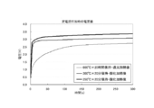
- FIG. 6 is a diagram showing X-ray diffraction results of an aluminum material having a coating layer made of a dielectric precursor formed on the surface after the coating layer forming step of Example 5 and the electrode structures obtained in Examples 5 to 7. is there. It is a figure which shows the X-ray-diffraction result of the electrode structure obtained in Example 7 and 8. It is a figure which shows the change of a voltage value when a DC constant current is sent through the electrode structure obtained in Example 6, 9, and 10.
- FIG. 6 is a diagram showing X-ray diffraction results of an aluminum material having a coating layer made of a dielectric precursor formed on the surface after the coating layer forming step of Example 5 and the electrode structures obtained in Examples 5 to 7. is there. It is a figure which shows the X-ray-diffraction result of the electrode structure obtained in Example 7 and 8. It is a figure which shows the change of a voltage value when a DC constant current is sent through the electrode structure obtained in Example 6, 9, and 10.
- FIG. 6 is a diagram showing X
- the electrode structure manufacturing method of the present invention includes a coating layer forming step of forming a coating layer made of a dielectric precursor containing a valve metal on the surface of an aluminum material, an aluminum material on which the coating layer is formed, carbon A reduction heating step of heating in a reducing atmosphere not included.
- Coating layer forming process In the method for manufacturing an electrode structure according to the present invention, first, a coating layer forming step of forming a coating layer made of a dielectric precursor containing a valve metal on the surface of an aluminum material is performed.
- the method for forming a coating layer made of a dielectric precursor containing a valve metal on the surface of an aluminum material as a substrate is not particularly limited, but a sol-gel method is preferably employed.
- a sol-gel method is preferably employed.
- a coating solution gelled from a solution (sol) containing oxide precursor particles as a dielectric precursor is used. Adjust and apply on the surface of the aluminum material.
- a coating liquid obtained by emulsifying valve metal-containing particles in a solution may be prepared and applied on the surface of an aluminum material.
- the application method is not particularly limited, and a spin coating method, a bar coating method, a flow coating method, or a dip coating method is appropriately employed.
- the thickness of the coating layer formed by coating can be controlled by the number of coatings, the composition and concentration of the coating solution.
- the aluminum material on which the coating layer made of the dielectric precursor containing the valve metal is formed on the surface is dried if necessary.
- Reduction heating process In the production method of the present invention, following the above-described coating layer forming step, reduction is performed by heating an aluminum material on which a coating layer made of a dielectric precursor containing a valve metal is formed in a reducing atmosphere not containing carbon. A heating process is performed.
- the reducing atmosphere is not particularly limited, as long as the reducing substance exists in the space where the aluminum material on which the coating layer made of the dielectric precursor material including the valve metal is formed is disposed. It may be used in any state such as gas.
- the reducing substance when the reducing substance is in the form of gas, the reducing substance is used alone in the sealed space where the aluminum material having the coating layer made of the dielectric precursor containing the valve metal is heated. Or a reducing substance may be filled together with an inert gas.
- the reducing substance is a liquid, the reducing substance may be filled alone, or the reducing substance may be filled together with an inert gas so as to vaporize in the sealed space. .
- the reducing substance is not particularly limited, and examples thereof include hydrogen, ammonia, hydrazine, hydrogen sulfide, etc. Among them, hydrogen is preferably used.
- the inert gas is not particularly limited, and specific examples include nitrogen, helium, neon, argon, krypton, xenon, and radon.
- the heating temperature may be appropriately set according to the composition of the aluminum material to be heated and the composition and thickness of the coating layer made of the dielectric precursor containing the valve metal, but is usually 450 ° C. or higher and lower than 660 ° C. It is preferably within the range, and more preferably within the range of 530 ° C. or more and 640 ° C. or less.
- the heating temperature is set to 450 ° C. or higher, at least a part of the coating layer made of a dielectric precursor containing a valve metal heated in a reducing atmosphere not containing carbon is reduced.
- heating the aluminum material on which the coating layer made of the dielectric precursor material including the valve metal is heated at a temperature lower than 450 ° C.
- the heating time depends on the heating temperature and the like, but generally it is preferably in the range of 1 hour to 100 hours.
- a coating layer containing a valve metal and having a conductive portion is formed on the surface of the aluminum material.
- This conductive portion is a portion in which at least a part of the coating layer made of the dielectric precursor containing the valve metal is reduced.
- An intervening layer containing aluminum and carbon is not formed between the aluminum material and the coating layer, but an intervening layer containing aluminum and oxygen is formed.
- an electrode structure that can suppress leakage current and suppress electrical short-circuit when in contact with an electrolyte is obtained. be able to.
- a coating layer since an intervening layer has an electroconductive part, it has a high electrostatic capacitance compared with the case where it does not have an electroconductive part.
- an oxidation heating step of further heating the obtained electrode structure of the present invention in an oxidizing atmosphere may be performed.
- the oxidizing atmosphere means that oxygen exists in the space in which the aluminum material on which the coating layer having a conductive portion is formed is arranged, may be filled with oxygen alone, or Further, oxygen may be filled together with a non-reducing gas.
- the oxidizing atmosphere is preferably a space containing 2 to 50% by volume of oxygen.
- the heating temperature may be appropriately set according to the withstand voltage required for the electrode structure, but is usually preferably in the range of 500 ° C. or lower, and more preferably in the range of 200 ° C. or higher and 400 ° C. or lower.
- the heating time depends on the heating temperature and the like, it is generally preferable that the heating time be in the range of 10 seconds to 50 hours.
- a coating layer containing a valve metal and having a conductive portion is formed, and at least a part of the coating layer has a reduced portion, and the particles constituting the coating layer have the outermost portion. At least a portion of the outer surface will have a more oxidized dielectric than the interior of the particle.
- the electrode structure thus obtained has a withstand voltage.
- an anodic oxidation step of further anodizing the obtained electrode structure of the present invention may be performed.
- the anodic oxidation step is not particularly limited, and may be performed at a voltage of 1 V or more and 100 V or less in a solution such as ammonium adipate.
- a coating layer containing a valve metal and having a conductive portion is formed, and at least a part of the coating layer is reduced, and particles constituting the coating layer At least a portion of the outermost surface of this will have a more oxidized dielectric than the interior of the particle.
- the electrode structure thus obtained also has a withstand voltage.
- the electrode structure obtained by the production method of the present invention can be applied not only to the anode material of the capacitor but also to the cathode material.
- the aluminum material as a base material on which a coating layer including a valve metal and having a conductive portion is formed is not particularly limited, and a pure aluminum or aluminum alloy foil is used. Can do.
- Such an aluminum material preferably has an aluminum purity of 98% by mass or more as a value measured according to the method described in “JIS H 2111”.
- the aluminum material used in the present invention has a composition of lead (Pb), silicon (Si), iron (Fe), copper (Cu), manganese (Mn), magnesium (Mg), chromium (Cr), zinc ( Zn alloy, titanium (Ti), vanadium (V), gallium (Ga), nickel (Ni), and aluminum alloy to which at least one alloy element is added within the necessary range, or the above inevitable It also includes aluminum with limited impurity element content.
- the thickness of the aluminum material is not particularly limited, but generally it is preferably in the range of 5 ⁇ m to 200 ⁇ m.
- the above-mentioned aluminum material can be manufactured by a known method. For example, a molten aluminum or aluminum alloy having the above predetermined composition is prepared, and an ingot obtained by casting this is appropriately homogenized. Then, the aluminum material used as a base material can be obtained by performing hot rolling and cold rolling to this ingot. In addition, you may perform an intermediate annealing process in the temperature range of 150 to 400 degreeC in the middle of said cold rolling process.
- the aluminum material may be appropriately pretreated before the step of forming the coating layer made of the dielectric precursor containing the valve metal (coating layer forming step).
- a coating layer containing a valve metal and having a conductive portion is formed on the surface of an aluminum material. Since the coating layer has a conductive portion, it has a higher capacitance than a case where it does not have a conductive portion.
- valve metal examples include, but are not limited to, magnesium, thorium, cadmium, tungsten, tin, iron, silver, silicon, tantalum, titanium, hafnium, aluminum, zirconium, niobium, and the like.
- titanium, tantalum, hafnium, Zirconium or niobium is preferably used.
- the thickness of the coating layer having a conductive portion is not particularly limited, but is preferably 0.01 ⁇ m or more and 100 ⁇ m or less, and more preferably 0.05 ⁇ m or more and 20 ⁇ m or less. If it is in this range, high electrostatic capacity can be secured in consideration of industrial productivity.
- the coating layer having a conductive portion is preferably composed of particles containing a valve metal.
- the size of the particles decreases as the surface of the coating layer having a conductive portion approaches the surface of the aluminum material.
- the particle size decreases from the surface of the coating layer having a conductive portion toward the surface of the aluminum material, the particle size increases at the surface layer of the coating layer, and the particle at the interface contacting the surface of the aluminum material on the opposite side. Is fine. Since the particles are large on the surface layer of the coating layer, the gaps between the particles are also large, and when used as an electrode structure, the conductive liquid substance can be easily infiltrated. Since the particles are fine at the interface in contact with the surface of the opposite aluminum material, a dense layer is formed.
- the particle size is preferably 1 nm or more and 1 ⁇ m or less. If the diameter of the particles constituting the coating layer is within the above range, the adhesion between the coating layer and the aluminum material is increased at the interface contacting the surface of the aluminum material, and the capacitance as the electrode structure is increased. In addition, it is advantageous to satisfy both the point of enlarging the surface area of the particles.
- the particle size is obtained by calculating the particle size by selecting 50 arbitrary particles from a photograph observed in a cross section with a scanning transmission electron microscope (STEM: Scanning Transmission Electron Microscopy), and calculating the particle size.
- the coating layer including the valve metal and having the conductive portion may be entirely composed of the conductive portion including the valve metal, or the dielectric layer including the valve metal and the valve metal You may comprise from the electroconductive part containing.
- the conductive portion has an oxidation number different from that of the portion other than the conductive portion and exists in at least a part of the particles.
- “part” means a part of one particle among the plurality of particles when attention is paid to one particle. If a part of one particle has conductivity, the other part may not have conductivity.
- the dielectric precursor containing the valve metal when the coating layer made of the dielectric precursor containing the valve metal is formed by the sol-gel method, before the reduction heating step, the dielectric precursor containing the valve metal is used.
- the resulting coating layer does not have electrical conductivity.
- the reduction heating process at least a part of the particles constituting the coating layer made of the dielectric precursor containing the valve metal is reduced, and a coating layer having a conductive portion is formed.
- the conductive portion is present in at least a part of the particles constituting the coating layer. Since the conductive portion is present in at least a part of the particles constituting the coating layer, it has a higher capacitance than when the conductive portion is not present in the particles.
- the particles containing the valve metal may be any kind of metal, oxide, hydroxide, sulfide, nitride, etc. as long as it contains the valve metal.
- an oxide is preferable.
- oxides containing valve metals include oxides such as magnesium, thorium, cadmium, tungsten, tin, iron, silver, silicon, tantalum, titanium, hafnium, aluminum, zirconium and niobium.
- the oxide containing the valve metal is an oxide of titanium
- Ti 2 O 5 , TiO 2 , Ti 2 O 3 , TiO and the like can be mentioned.
- these titanium oxides low-order titanium oxides represented by Ti n O 2n-1 such as TiO and Ti 2 O 3 are said to exhibit relatively good conductivity. Therefore, when the coating layer containing the valve metal and having the conductive portion formed after the reduction heating step is composed of particles containing an oxide of titanium, the dielectric precursor containing the valve metal is used. It is presumed that low-order titanium oxides exhibiting conductivity as described above are present in at least a part of the particles constituting the coating layer by reducing at least a part of the particles constituting the coating layer.
- the conductive portion has an oxidation number different from that of the portion other than the conductive portion (the oxidation number of the conductive portion is lower (small value) than the oxidation number of the portion other than the conductive portion).
- the particles constituting the coating layer may be composed of a conductive portion made of a low-order oxide having a low oxidation number and a dielectric portion made of a high-order oxide having a high oxidation number. It can be said that the particles constituting the coating layer may be composed of only a conductive portion made of a low-order oxide having a low oxidation number.
- the state of (particles including the valve metal) constituting the (conductive coating layer) further changes.
- the particles include an inside and an outermost surface located outside the inside, and at least a part of the outermost surface has a dielectric that is oxidized from the inside.
- the electrode structure has a withstand voltage.
- the titanium oxide as an example, at least a part of the particles constituting the coating layer made of the dielectric precursor containing the valve metal is reduced by the reduction heating step, and TiO, Ti 2 O 3 varies the low-order titanium oxides showing a relatively good conductivity, denoted by Ti n O 2n-1 equal, by subsequent oxidation heating step or anodic oxidation process, the particles are oxidized, of the particles It is inferred that at least a part of the outermost surface is oxidized more than the inside of the particle (in other words, the oxidation number is higher order), and at least a part of the outermost surface is changed to a dielectric. Is done.
- the particles constituting the coating layer are composed of a dielectric portion (inside) made of a high-order oxide having a high oxidation number, and a conductive portion (intermediate portion) made of a low-order oxide having a low oxidation number.
- a dielectric portion (outermost surface) made of a high-order oxide having a high oxidation number, and the particles constituting the coating layer are electrically conductive made of a low-order oxide having a low oxidation number It can be said that it may be composed of a portion (inside) and a dielectric portion (outermost surface) made of a high-order oxide having a high oxidation number.
- oxides having different oxidation numbers can be confirmed, for example, by performing X-ray diffraction (XRD) of the electrode structure.
- XRD X-ray diffraction
- the electrode structure of the present invention includes an intervening layer containing aluminum and oxygen between the aluminum material and the coating layer.
- This intervening layer is formed through the reduction heating process described above.
- the presence of the intervening layer has an effect of improving the adhesion between the aluminum material and the coating layer.
- this intervening layer does not contain carbon, it does not cause an increase in leakage current, nor does it cause an electrical short circuit when in contact with the electrolyte.
- the intervening layer is preferably formed in at least a part of the surface of the aluminum material.
- the intervening layer is more preferably an aluminum oxide.
- the surface of the aluminum material usually has an aluminum oxide film (natural oxide film) formed naturally.
- the surface of the aluminum material before carrying out each step in the manufacturing method of the electrode structure of the present invention has a natural oxide film of aluminum, but the aluminum oxide constituting the intervening layer is A mode different from a natural oxide film is clearly shown.
- the intervening layer containing oxygen is thicker than the natural oxide film of the aluminum material and is locally formed.
- the shape of the intervening layer is not particularly limited.
- an intervening layer in which crystal nuclei are dispersed between the aluminum material and the coating layer has an electrical resistance at the interface between the coating layer and the aluminum material. This is preferable in that it suppresses the increase in the amount.
- the thickness of the intervening layer is not particularly limited, for example, an intervening layer having a thickness of 10 nm to 500 nm is preferable in terms of preventing an increase in electrical resistance.
- the electrode structure of the present invention can be used as a capacitor electrode material.
- the type of the capacitor is not particularly limited, and examples thereof include a solid electrolytic capacitor and a liquid electrolytic capacitor.
- the electrode structure of the present invention can be used not only as a cathode of a capacitor but also as an anode.
- Electrode structures were produced according to the following Examples 1 to 10 and Comparative Examples 1 to 4.
- Example 1 Comparative Example 1
- An aluminum foil having a thickness of 50 ⁇ m and a purity of 99.3% by mass was immersed in a titanium alkoxide solution to form a coating layer made of a dielectric precursor having a thickness of 0.15 ⁇ m on both surfaces.
- the composition of the titanium alkoxide solution was as follows: Ti (n-OC 4 H 9 ) 4 : 0.15 mol, CH 3 COCH 2 COCH 3 : 0.45 mol, C 2 H 5 OH: 18 mol, H 2 O: 0. 3 mol.
- the aluminum foil was immersed in the titanium alkoxide solution for 3 seconds in an environment with a humidity of 40% or less, and then heated and dried in air at a temperature of 100 ° C. for 10 minutes. The above immersion treatment and heat treatment were repeated three times to form a coating layer made of a dielectric precursor.
- the aluminum material on which the coating layer made of the dielectric precursor is formed is held at a temperature of 600 ° C. for 10 hours in a hydrogen gas atmosphere in Example 1 and in a methane gas atmosphere in Comparative Example 1, respectively. As a result, an electrode structure was obtained.
- Example 2 The electrode structure obtained in Example 1 was held in air at a temperature of 300 ° C. for 10 minutes to obtain an electrode structure of Example 2.
- Example 3 The electrode structure of Example 3 was obtained by anodizing the electrode structure obtained in Example 1 at a voltage of 2V.
- the anodic oxidation conditions were such that a direct current of 50 mA / cm 2 was passed in a 15% by mass ammonium adipate aqueous solution at a temperature of 85 ° C. and held for 10 minutes after the voltage reached 2V.
- Example 4 The electrode structure of Example 4 was obtained by anodizing the electrode structure obtained in Example 2 at a voltage of 2V.
- the anodic oxidation conditions were such that a direct current of 50 mA / cm 2 was passed in a 15% by mass ammonium adipate aqueous solution at a temperature of 85 ° C. and held for 10 minutes after the voltage reached 2V.
- Examples 5 to 7 Using the same aluminum foil and titanium alkoxide solution as in Example 1, the immersion treatment and heat treatment performed in Example 1 were repeated about 6 to 10 times, and consisted of a dielectric precursor having a thickness of 1.0 ⁇ m on both sides.
- the aluminum material with the coating layer formed on the surface was held in a hydrogen gas atmosphere at a temperature of 600 ° C. for 5 hours, 20 hours, and 40 hours. An electrode structure was obtained.
- Example 8 The electrode structure obtained in Example 7 was held in air at a temperature of 350 ° C. for 2 minutes to obtain an electrode structure of Example 8.
- Example 9 The electrode structure obtained in Example 6 was held in air at a temperature of 300 ° C. for 20 minutes in Example 9 and in Example 10 for 20 minutes at a temperature of 350 ° C. to obtain an electrode structure.
- Comparative Example 2 The electrode structure obtained in Comparative Example 1 was held in air at a temperature of 300 ° C. for 10 minutes to obtain an electrode structure of Comparative Example 2.
- Comparative Example 3 An electrode structure of Comparative Example 3 was obtained by anodizing the electrode structure obtained in Comparative Example 1 at a voltage of 2V.
- the anodic oxidation conditions were such that a direct current of 50 mA / cm 2 was passed in a 15% by mass ammonium adipate aqueous solution at a temperature of 85 ° C. and held for 10 minutes after the voltage reached 2V.
- Comparative Example 4 An aluminum foil having a thickness of 100 ⁇ m and a purity of 99.9% by mass was AC-etched and anodized at a voltage of 2 V to obtain an electrode structure of Comparative Example 4.
- Electrolyte composition (12 wt% hydrochloric acid + 1 wt% sulfuric acid + 100 g aluminum chloride) / liter Temperature: 50 ° C.
- Current waveform Sine wave AC Frequency: 60Hz Current density: 200 mA / cm 2 Time: 60 seconds
- Electrolyte composition (20 wt% hydrochloric acid + 3 wt% sulfuric acid + 100 g aluminum chloride) / liter Temperature: 60 ° C. Time: 120 seconds
- Electrolyte composition (12 wt% hydrochloric acid + 1 wt% sulfuric acid + 100 g aluminum chloride) / liter Temperature: 30 ° C.
- Current waveform Sine wave AC Frequency: 60Hz Current density: 160 mA / cm 2 Time: 300 seconds
- the anodic oxidation conditions were such that a direct current of 50 mA / cm 2 was passed in a 15% by mass ammonium adipate aqueous solution at a temperature of 85 ° C. and held for 10 minutes after the voltage reached 2V.
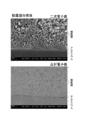
- Example 6 (1) a cross section of an aluminum material on which a coating layer made of a dielectric precursor was formed after the coating layer forming step, and (2) a temperature in a hydrogen gas atmosphere in the subsequent reduction heating step
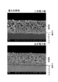
- FIGS. 1 and 2 show photographs obtained by observing, with a field emission scanning electron microscope, a cross section of the electrode structure of Example 6 obtained by holding at 600 ° C. for 20 hours.
- the upper photograph is a secondary electron image
- the lower photograph is a reflected electron image.
- fine particles having a particle diameter of less than 50 nm, which is a dielectric precursor containing a valve metal are uniformly present in the coating layer formed on the surface of the aluminum material.
- the upper photograph is the secondary electron image
- the lower photograph is the reflected electron image.
- particles that are dielectric precursors including a valve metal grow in the coating layer formed on the surface of the aluminum material, and there are particles having a particle size of less than 200 nm. And it turns out that a particle size becomes small as it approaches the surface of an aluminum material from the surface layer of a coating layer.
- a compound having a composition different from that of the aluminum material is present in a dispersed form in the intervening layer between the aluminum material and the coating layer. Recognize.
- Example 1 using a high-resolution scanning transmission electron microscope (STEM: Scanning Transmission Electron Microscopy) (TITI 80-300 manufactured by FEI), an intervening layer between the aluminum material and the coating layer was used. Identification of existing compounds was performed.
- STEM Scanning Transmission Electron Microscopy
- the cross section was observed with a scanning transmission electron microscope, and energy dispersive X-ray analysis (EDX: Energy Dispersive X-ray spectrocopy) was performed at two locations in the aluminum material and the intervening layer.
- EDX Energy Dispersive X-ray spectrocopy
- FIG. 3 shows a high-angle scattering dark field image (HAADF) observed with the STEM of the electrode structure of Example 1.
- HAADF high-angle scattering dark field image
- Table 1 shows the quantitative analysis results of the aluminum component and oxygen component at each point shown in FIG.
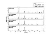
- FIG. 4 shows the results of X-ray diffraction (XRD: RINT2000 manufactured by Rigaku) on the body.
- X-ray diffraction was performed by a thin film X-ray diffraction method using Cu—K ⁇ rays, an acceleration voltage of 40 kV, a scanning axis 2 ⁇ ranging from 5 ° to 80 °.
- the uppermost curve in FIG. 4 shows the X-ray diffraction peak intensity of an aluminum material on the surface of which a coating layer made of a dielectric precursor is formed after the coating layer forming step of Example 5. From this curve, it can be seen that the aluminum peak of the aluminum material and the peak of TiO 2 (anatase) as the dielectric precursor containing the valve metal were detected.
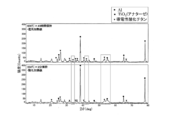
- the results of X-ray diffraction performed on the electrode structures of Example 7 and Example 8 are shown in FIG.
- the upper curve in FIG. 5 shows the X-ray diffraction peak intensity of the electrode structure of Example 7, and the lower curve in FIG. 5 shows the X-ray diffraction peak intensity of the electrode structure of Example 8.
- the X-ray diffraction peak intensity of Example 8 is higher than the X-ray diffraction peak intensity of Example 7, and the TiO 2 (anatase) peak of the dielectric precursor containing a valve metal and the conductive titanium oxide. It can be seen that the peak of is broad, the peak of the conductive titanium oxide becomes smaller overall, and some of the peak disappears.
- Example 8 This is because partly conductive titanium oxide reacts with oxygen and is oxidized because oxidation heating is performed in Example 8. From the above, it can be seen that at least a part of the conductive titanium oxide portion formed by reduction in the reduction heating step is oxidized after the oxidation heating step, so that the coating layer has a dielectric portion. .
- a reference electrode and a counter electrode terminal are connected to the foil, a 0.1 mA / cm 2 direct current is passed in a 15% by mass ammonium adipate aqueous solution at a temperature of 25 ° C., and the voltage value at that time is 5 minutes. It was measured.
- the electrode structure has a withstand voltage by performing the oxidation heating step, at least a part of the outermost surface such as particles constituting the coating layer containing the valve metal is oxidized more than the inside. It can be seen that it has a dielectric.
- a carbon layer as a cathode lead layer was formed thereon, and a silver layer was further formed on the carbon layer.
- a sandpaper the surface portion of the coating layer of the sample where the solid electrolyte layer / carbon layer / silver layer was not formed was scraped off to expose the aluminum part.
- Each terminal of an LCR meter (LCR HiTester 3522-50 manufactured by Hioki Electric Co., Ltd.) was pressed against each surface of the aluminum part and the silver layer of the test sample thus prepared, and the frequency was 120 Hz and the measurement voltage was 0.05 Vrms. The resistance value was measured under the conditions. In addition, the distance between the parts which press each terminal was 3 cm.
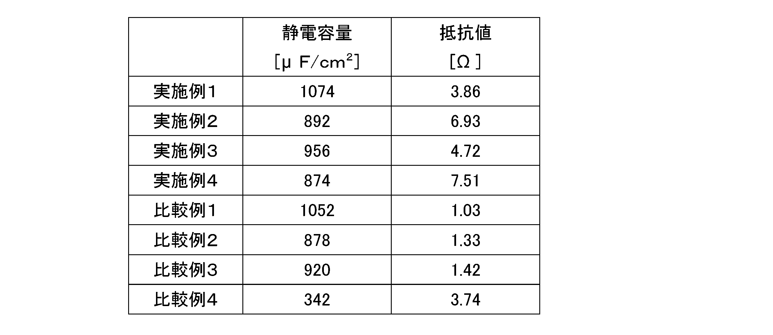
- Table 3 shows the above evaluation results.
- an electrode structure that can suppress a leakage current, has a high capacitance, and suppresses an electrical short-circuit when in contact with an electrolyte.
- an electrode structure that can also be used as an anode of a capacitor can be obtained by preferably having a withstand voltage.
Landscapes
- Engineering & Computer Science (AREA)
- Power Engineering (AREA)
- Microelectronics & Electronic Packaging (AREA)
- Chemical & Material Sciences (AREA)
- Materials Engineering (AREA)
- Manufacturing & Machinery (AREA)
- Other Surface Treatments For Metallic Materials (AREA)
- Solid-Phase Diffusion Into Metallic Material Surfaces (AREA)
- Fixed Capacitors And Capacitor Manufacturing Machines (AREA)
- Electric Double-Layer Capacitors Or The Like (AREA)
Abstract
Description
本発明の電極構造体の製造方法は、バルブ金属を含む誘電体前駆物質からなる被覆層をアルミニウム材の表面上に形成する被覆層形成工程と、被覆層が形成されたアルミニウム材を、炭素を含まない還元性雰囲気中で加熱する還元加熱工程とを備える。
本発明の電極構造体の製造方法においては、まず、バルブ金属を含む誘電体前駆物質からなる被覆層をアルミニウム材の表面上に形成する被覆層形成工程を行なう。
本発明の製造方法においては、上記の被覆層形成工程に続いて、バルブ金属を含む誘電体前駆物質からなる被覆層が形成されたアルミニウム材を、炭素を含まない還元性雰囲気中で加熱する還元加熱工程を行なう。
前述の還元加熱工程の後に、得られた本発明の電極構造体を酸化性雰囲気中でさらに加熱する酸化加熱工程を行なってもよい。
前述の加熱工程の後に、得られた本発明の電極構造体をさらに陽極酸化する陽極酸化工程を行なってもよい。
本発明の一つの実施形態として、バルブ金属を含み、かつ、導電性部分を有する被覆層が形成される基材としてのアルミニウム材は、特に限定されず、純アルミニウムまたはアルミニウム合金の箔を用いることができる。このようなアルミニウム材は、アルミニウム純度が「JIS H 2111」に記載された方法に準じて測定された値で98質量%以上のものが好ましい。本発明で用いられるアルミニウム材は、その組成として、鉛(Pb)、珪素(Si)、鉄(Fe)、銅(Cu)、マンガン(Mn)、マグネシウム(Mg)、クロム(Cr)、亜鉛(Zn)、チタン(Ti)、バナジウム(V)、ガリウム(Ga)、ニッケル(Ni)およびホウ素(B)の少なくとも1種の合金元素を必要範囲内において添加したアルミニウム合金、または、上記の不可避的不純物元素の含有量を限定したアルミニウムも含む。アルミニウム材の厚みは、特に限定されないが、一般的には5μm以上200μm以下の範囲内とするのが好ましい。
本発明の電極構造体は、上述のように、アルミニウム材の表面上には、バルブ金属を含み、かつ、導電性部分を有する被覆層が形成されている。被覆層は導電性部分を有するので、導電性部分を有していない場合に比べて、高い静電容量を有する。
本発明の電極構造体は、アルミニウム材と被覆層との間にアルミニウムと酸素を含む介在層とを備える。この介在層は、上述の還元加熱工程を経ることで形成される。この介在層が存在することにより、アルミニウム材と被覆層の密着性を高めるという効果を奏する。また、この介在層は、炭素を含まないので、漏れ電流が増大する原因にならず、電解質に接した場合に電気的に短絡する原因にもならない。
本発明の電極構造体は、コンデンサの電極材料として使用できる。コンデンサの種類は特に限定されないが、たとえば、固体電解コンデンサ、液体電解コンデンサ等が挙げられる。また、本発明の電極構造体は、コンデンサの陰極として利用できるだけでなく、陽極としても利用できる。
厚みが50μmで純度が99.3質量%のアルミニウム箔をチタンアルコキシド溶液に浸漬し、両面に厚みが0.15μmの誘電体前駆物質からなる被覆層を形成した。
実施例1で得られた電極構造体を、空気中にて温度300℃で10分間保持し、実施例2の電極構造体を得た。
実施例1で得られた電極構造体を電圧2Vで陽極酸化することにより、実施例3の電極構造体を得た。なお、陽極酸化条件は、温度が85℃の15質量%アジピン酸アンモニウム水溶液中で、50mA/cm2の直流電流を流し、電圧が2Vに達した後10分間保持することにした。
実施例2で得られた電極構造体を電圧2Vで陽極酸化することにより、実施例4の電極構造体を得た。なお、陽極酸化条件は、温度が85℃の15質量%アジピン酸アンモニウム水溶液中で、50mA/cm2の直流電流を流し、電圧が2Vに達した後10分間保持することにした。
実施例1と同じアルミニウム箔およびチタンアルコキシド溶液を使用し、実施例1で行った浸漬処理と加熱処理を6回~10回程度繰り返して、両面に厚みが1.0μmの誘電体前駆物質からなる被覆層が表面に形成されたアルミニウム材を、水素ガス雰囲気中にて、温度600℃で5時間保持、20時間保持、40時間保持して、それぞれ順に実施例5、実施例6、実施例7の電極構造体を得た。
実施例7で得られた電極構造体を、空気中にて温度350℃で2分間保持し、実施例8の電極構造体を得た。
実施例6で得られた電極構造体を、空気中にて、実施例9では温度300℃で20分間保持、実施例10では温度350℃で20分間保持して電極構造体を得た。
比較例1で得られた電極構造体を空気中にて温度300℃で10分間保持し、比較例2の電極構造体を得た。
比較例1で得られた電極構造体を電圧2Vで陽極酸化することにより、比較例3の電極構造体を得た。なお、陽極酸化条件は、温度が85℃の15質量%アジピン酸アンモニウム水溶液中で、50mA/cm2の直流電流を流し、電圧が2Vに達した後10分間保持することにした。
厚みが100μmで純度が99.9質量%のアルミニウム箔を交流エッチングし、電圧2Vで陽極酸化することにより、比較例4の電極構造体を得た。
電解液組成:(12wt%塩酸+1wt%硫酸+100g塩化アルミニウム)/リットル
温度:50℃
電流波形:正弦波交流
周波数:60Hz
電流密度:200mA/cm2
時間:60秒
電解液組成:(20wt%塩酸+3wt%硫酸+100g塩化アルミニウム)/リットル
温度:60℃
時間:120秒
電解液組成:(12wt%塩酸+1wt%硫酸+100g塩化アルミニウム)/リットル
温度:30℃
電流波形:正弦波交流
周波数:60Hz
電流密度:160mA/cm2
時間:300秒
高分解能の電界放射型走査電子顕微鏡(FE-SEM: field emission SEM)(Carl Zeiss製Ultra55)を用いて行った。

実施例5の被覆層形成工程後に誘電体前駆物質からなる被覆層が表面に形成されたアルミニウム材、および、水素ガス雰囲気中にて温度600℃で各時間保持した実施例5~7の電極構造体について、X線回折(XRD:X-ray diffraction)(Rigaku製RINT2000)を行った結果を図4に示す。X線回折は、Cu-Kα線を用い、加速電圧が40kVで、走査軸2θを5°から80°までの範囲とし、薄膜X線回折法によって行った。
実施例6、9、10で作製した電極構造体の被覆層上の一部に被覆層の露出面積が1cm2となるようにマスキングを行った。サンドペーパーを用いて、この試料の端部において表層の被覆層を削り落としてアルミニウム材部を露出させた。このようにして作製された試験試料のアルミニウム材部に電気化学システム(北斗電工株式会社製 HZ-3000)の作用電極端子を接続し、厚みが150μmで純度が99.99質量%の高純度アルミニウム箔に参照電極と対極の端子とを接続して、温度が25℃の15質量%アジピン酸アンモニウム水溶液中で、0.1mA/cm2の直流定電流を流し、その際の電圧値を5分間測定した。
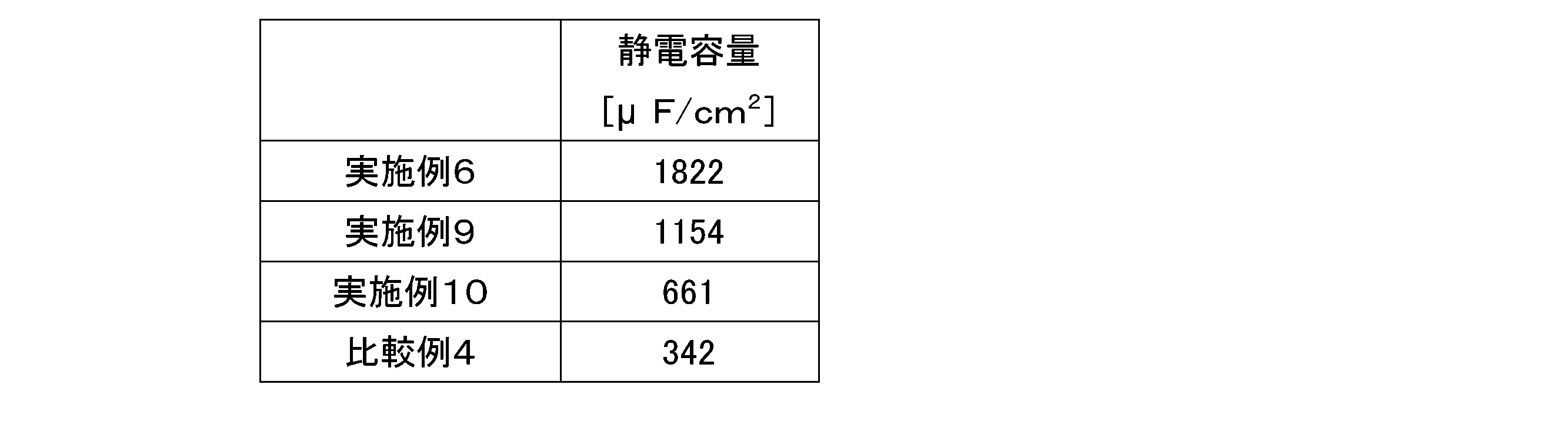
実施例1~4、比較例1~4の電極構造体についても、EIAJ規格に定める電解コンデンサ用極低圧用化成箔の静電容量測定方法に基づき、静電容量の評価を行った。
実施例1~4、比較例1~4の電極構造体を陽極とし、被覆層上の一部に被覆層の露出面積が1cm2となるようにマスキングを行い、露出した被覆層上に、導電性高分子のモノマーとして3,4-エチレンジオキシチオフェンと、酸化剤であるp-トルエンスルホン酸第二鉄と、溶媒のエタノールとを混合した溶液を塗布した後に、105℃の温度で1時間加熱して化学重合させることによって、陰極である固体電解質層を形成した。その上に陰極引出層であるカーボン層を形成し、さらにカーボン層の上に銀層を形成した。サンドペーパーを用いて、この試料の固体電解質層/カーボン層/銀層を形成していない一部において表層の被覆層を削り落としてアルミニウム部を露出させた。このようにして作製された試験試料のアルミニウム部と銀層の各表面に、LCRメーター(日置電機株式会社製 LCRハイテスタ3522-50)の各端子を押し当て、周波数120Hz、測定電圧0.05Vrmsの条件で抵抗値を測定した。なお、各端子を押し当てる部位の間の距離は3cmとした。抵抗値が高いほど、電極構造体の表面に漏れ電流の少ない、健全な被膜が形成されているといえる。また、コンデンサの陽極として一般的に用いられる、化成エッチド箔である比較例4と同等以上の抵抗値であれば問題ないといえる。
Claims (12)
- バルブ金属を含む誘電体前駆物質からなる被覆層をアルミニウム材の表面上に形成する被覆層形成工程と、
前記被覆層が形成された前記アルミニウム材を、炭素を含まない還元性雰囲気中で加熱する還元加熱工程と、
を備えた、電極構造体の製造方法。 - 前記還元性雰囲気は、水素を含む雰囲気である、請求項1に記載の電極構造体の製造方法。
- 前記還元加熱工程は、450℃以上660℃未満の温度範囲で行われる、請求項1に記載の電極構造体の製造方法。
- 前記還元加熱工程の後、前記アルミニウム材を酸化性雰囲気中で加熱する酸化加熱工程をさらに備える、請求項1に記載の電極構造体の製造方法。
- 前記還元加熱工程の後、前記アルミニウム材を陽極酸化する陽極酸化工程をさらに備える、請求項1に記載の電極構造体の製造方法。
- アルミニウム材と、
前記アルミニウム材の表面上に形成された、バルブ金属を含み、かつ、導電性部分を有する被覆層と、
前記アルミニウム材と前記被覆層との間に形成された、アルミニウムと酸素を含む介在層と、
を備えた、電極構造体。 - 前記介在層は、前記アルミニウム材の表面の少なくとも一部の領域に形成されている、請求項6に記載の電極構造体。
- 前記介在層は、アルミニウム酸化物である、請求項6に記載の電極構造体。
- 前記バルブ金属は、マグネシウム、トリウム、カドミウム、タングステン、錫、鉄、銀、シリコン、タンタル、チタン、ハフニウム、アルミニウム、ジルコニウム、および、ニオブからなる群より選ばれた一種以上である、請求項6に記載の電極構造体。
- 前記被覆層は、バルブ金属を含む粒子から構成され、前記導電性部分が、前記導電性部分以外の部分と異なる酸化数を有し、かつ、前記粒子の少なくとも一部に存在する、請求項6に記載の電極構造体。
- 前記粒子は、内部と、内部よりも外側に位置する最外表面とを含み、前記最外表面の少なくとも一部が、前記内部よりも酸化された誘電体を含む、請求項10に記載の電極構造体。
- 請求項6に記載の電極構造体を備えた、コンデンサ。
Priority Applications (5)
| Application Number | Priority Date | Filing Date | Title |
|---|---|---|---|
| KR1020127017375A KR20130076793A (ko) | 2010-04-07 | 2011-03-30 | 전극 구조체의 제조 방법, 전극 구조체 및 콘덴서 |
| CN201180017487.9A CN102822919B (zh) | 2010-04-07 | 2011-03-30 | 电极结构体的制造方法、电极结构体以及电容器 |
| JP2011532438A JP4834193B2 (ja) | 2010-04-07 | 2011-03-30 | 電極構造体の製造方法、電極構造体およびコンデンサ |
| EP11765621A EP2557578A1 (en) | 2010-04-07 | 2011-03-30 | Method of manufacturing electrode structure, electrode structure, and capacitor |
| US13/513,958 US20120261162A1 (en) | 2010-04-07 | 2011-03-30 | Method for manufacturing electrode structure, electrode structure, and capacitor |
Applications Claiming Priority (2)
| Application Number | Priority Date | Filing Date | Title |
|---|---|---|---|
| JP2010088243 | 2010-04-07 | ||
| JP2010-088243 | 2010-04-07 |
Publications (1)
| Publication Number | Publication Date |
|---|---|
| WO2011125721A1 true WO2011125721A1 (ja) | 2011-10-13 |
Family
ID=44762664
Family Applications (1)
| Application Number | Title | Priority Date | Filing Date |
|---|---|---|---|
| PCT/JP2011/057985 Ceased WO2011125721A1 (ja) | 2010-04-07 | 2011-03-30 | 電極構造体の製造方法、電極構造体およびコンデンサ |
Country Status (7)
| Country | Link |
|---|---|
| US (1) | US20120261162A1 (ja) |
| EP (1) | EP2557578A1 (ja) |
| JP (1) | JP4834193B2 (ja) |
| KR (1) | KR20130076793A (ja) |
| CN (1) | CN102822919B (ja) |
| TW (1) | TWI470660B (ja) |
| WO (1) | WO2011125721A1 (ja) |
Cited By (2)
| Publication number | Priority date | Publication date | Assignee | Title |
|---|---|---|---|---|
| JP2013077676A (ja) * | 2011-09-30 | 2013-04-25 | Toyo Aluminium Kk | 電極構造体の製造方法、電極構造体およびコンデンサ |
| WO2013191162A1 (ja) * | 2012-06-20 | 2013-12-27 | 東洋アルミニウム株式会社 | 光触媒被覆材料、物品および光触媒被覆材料の製造方法 |
Families Citing this family (3)
| Publication number | Priority date | Publication date | Assignee | Title |
|---|---|---|---|---|
| CN103280327A (zh) * | 2013-05-16 | 2013-09-04 | 陶荣燕 | 高介电常数电极箔制备方法 |
| CN110648849B (zh) * | 2019-09-26 | 2021-12-14 | 宇启材料科技南通有限公司 | 一种阀金属多孔体涂层电极箔及制作方法和电解电容器 |
| US12002631B2 (en) * | 2021-10-20 | 2024-06-04 | KYOCERA AVX Components Corporation | Electrodeposited dielectric for a solid electrolytic capacitor |
Citations (8)
| Publication number | Priority date | Publication date | Assignee | Title |
|---|---|---|---|---|
| JPS62222512A (ja) | 1986-03-20 | 1987-09-30 | キヤノン株式会社 | 誘電体材料 |
| JPH10182221A (ja) | 1996-10-22 | 1998-07-07 | Lucent Technol Inc | 容量性素子を有する物品 |
| JPH11317331A (ja) | 1998-03-03 | 1999-11-16 | Acktar Ltd | 高表面積フォイル電極の製造法 |
| WO2002062569A1 (fr) | 2001-02-05 | 2002-08-15 | Ct For Advanced Science & Tech | Structure a couche d'oxyde, procede de production de cette structure, et condensateur et filtre utilisant cette structure |
| JP2003055796A (ja) | 2001-08-09 | 2003-02-26 | Showa Denko Kk | アルミニウム材およびその製造方法、ならびに電子写真用感光体および電解コンデンサ電極用アルミニウム材料 |
| JP2004259932A (ja) | 2003-02-26 | 2004-09-16 | Sumitomo Light Metal Ind Ltd | 電解コンデンサ電極用アルミニウム箔およびその製造方法 |
| WO2007055121A1 (ja) | 2005-11-10 | 2007-05-18 | Toyo Aluminium Kabushiki Kaisha | 電極構造体、コンデンサおよび電極構造体の製造方法 |
| JP2007169690A (ja) * | 2005-12-20 | 2007-07-05 | Mitsubishi Alum Co Ltd | 電解コンデンサ用アルミニウム箔 |
Family Cites Families (12)
| Publication number | Priority date | Publication date | Assignee | Title |
|---|---|---|---|---|
| US6416730B1 (en) * | 1998-09-16 | 2002-07-09 | Cabot Corporation | Methods to partially reduce a niobium metal oxide oxygen reduced niobium oxides |
| TWI285385B (en) * | 2003-02-19 | 2007-08-11 | Matsushita Electric Industrial Co Ltd | Solid electrolytic capacitor and method for manufacturing same |
| US7551424B2 (en) * | 2004-03-30 | 2009-06-23 | Rohm Co., Ltd. | Solid electrolytic capacitor |
| CN101689429B (zh) * | 2007-04-20 | 2013-05-08 | 富士通株式会社 | 电极箔及其制造方法以及电解电容器 |
| JP4978509B2 (ja) * | 2008-02-22 | 2012-07-18 | 富士通株式会社 | 電極箔の製造方法 |
| DE102008026304A1 (de) * | 2008-06-02 | 2009-12-03 | H.C. Starck Gmbh | Verfahren zur Herstellung von Elektrolytkondensatoren mit niedrigem Leckstrom |
| WO2010058552A1 (ja) * | 2008-11-19 | 2010-05-27 | 三洋電機株式会社 | コンデンサ用電極体およびコンデンサ |
| JP5542801B2 (ja) * | 2009-03-23 | 2014-07-09 | 東洋アルミニウム株式会社 | 電極構造体、コンデンサ、電池および電極構造体の製造方法 |
| CN101651047B (zh) * | 2009-07-22 | 2011-02-09 | 电子科技大学 | 一种Al2O3/Nb2O5复合介质膜铝电极箔的制备方法 |
| CN101651046B (zh) * | 2009-07-22 | 2011-05-11 | 电子科技大学 | 一种Al2O3/TiO2复合介质膜铝电极箔的制备方法 |
| JPWO2011043059A1 (ja) * | 2009-10-09 | 2013-03-04 | パナソニック株式会社 | 電極箔およびこれを用いたコンデンサ |
| WO2011099260A1 (ja) * | 2010-02-15 | 2011-08-18 | パナソニック株式会社 | 電極箔とその製造方法、電極箔を用いたコンデンサ |
-
2011
- 2011-03-30 KR KR1020127017375A patent/KR20130076793A/ko not_active Withdrawn
- 2011-03-30 WO PCT/JP2011/057985 patent/WO2011125721A1/ja not_active Ceased
- 2011-03-30 US US13/513,958 patent/US20120261162A1/en not_active Abandoned
- 2011-03-30 CN CN201180017487.9A patent/CN102822919B/zh not_active Expired - Fee Related
- 2011-03-30 JP JP2011532438A patent/JP4834193B2/ja not_active Expired - Fee Related
- 2011-03-30 EP EP11765621A patent/EP2557578A1/en not_active Withdrawn
- 2011-04-07 TW TW100111964A patent/TWI470660B/zh not_active IP Right Cessation
Patent Citations (8)
| Publication number | Priority date | Publication date | Assignee | Title |
|---|---|---|---|---|
| JPS62222512A (ja) | 1986-03-20 | 1987-09-30 | キヤノン株式会社 | 誘電体材料 |
| JPH10182221A (ja) | 1996-10-22 | 1998-07-07 | Lucent Technol Inc | 容量性素子を有する物品 |
| JPH11317331A (ja) | 1998-03-03 | 1999-11-16 | Acktar Ltd | 高表面積フォイル電極の製造法 |
| WO2002062569A1 (fr) | 2001-02-05 | 2002-08-15 | Ct For Advanced Science & Tech | Structure a couche d'oxyde, procede de production de cette structure, et condensateur et filtre utilisant cette structure |
| JP2003055796A (ja) | 2001-08-09 | 2003-02-26 | Showa Denko Kk | アルミニウム材およびその製造方法、ならびに電子写真用感光体および電解コンデンサ電極用アルミニウム材料 |
| JP2004259932A (ja) | 2003-02-26 | 2004-09-16 | Sumitomo Light Metal Ind Ltd | 電解コンデンサ電極用アルミニウム箔およびその製造方法 |
| WO2007055121A1 (ja) | 2005-11-10 | 2007-05-18 | Toyo Aluminium Kabushiki Kaisha | 電極構造体、コンデンサおよび電極構造体の製造方法 |
| JP2007169690A (ja) * | 2005-12-20 | 2007-07-05 | Mitsubishi Alum Co Ltd | 電解コンデンサ用アルミニウム箔 |
Cited By (2)
| Publication number | Priority date | Publication date | Assignee | Title |
|---|---|---|---|---|
| JP2013077676A (ja) * | 2011-09-30 | 2013-04-25 | Toyo Aluminium Kk | 電極構造体の製造方法、電極構造体およびコンデンサ |
| WO2013191162A1 (ja) * | 2012-06-20 | 2013-12-27 | 東洋アルミニウム株式会社 | 光触媒被覆材料、物品および光触媒被覆材料の製造方法 |
Also Published As
| Publication number | Publication date |
|---|---|
| JPWO2011125721A1 (ja) | 2013-07-08 |
| JP4834193B2 (ja) | 2011-12-14 |
| KR20130076793A (ko) | 2013-07-08 |
| TW201212073A (en) | 2012-03-16 |
| CN102822919B (zh) | 2015-08-19 |
| US20120261162A1 (en) | 2012-10-18 |
| EP2557578A1 (en) | 2013-02-13 |
| CN102822919A (zh) | 2012-12-12 |
| TWI470660B (zh) | 2015-01-21 |
Similar Documents
| Publication | Publication Date | Title |
|---|---|---|
| Achour et al. | Titanium nitride films for micro-supercapacitors: Effect of surface chemistry and film morphology on the capacitance | |
| JP5762501B2 (ja) | 電極構造体、コンデンサおよび電池 | |
| JP4275187B2 (ja) | 電解コンデンサ | |
| JP4274857B2 (ja) | 電解コンデンサの製造方法 | |
| TWI466154B (zh) | Electrode for electrolytic capacitor for electrolysis and method for manufacturing the same | |
| TWI493581B (zh) | Electrode material for electrolytic capacitor and its manufacturing method | |
| JP2010500771A (ja) | 構造化した焼結活性表面を有する半製品およびその製造方法 | |
| JP4834193B2 (ja) | 電極構造体の製造方法、電極構造体およびコンデンサ | |
| WO2002049965A1 (fr) | Procede de formation d'une couche d'oxyde de titane et d'un condensateur electrolytique au titane | |
| JP4965455B2 (ja) | 電極構造体、コンデンサおよび電極構造体の製造方法 | |
| JP5851667B1 (ja) | コンデンサ陽極体、固体電解コンデンサ素子、固体電解コンデンサおよびコンデンサ陽極体の製造方法 | |
| JP2013077676A (ja) | 電極構造体の製造方法、電極構造体およびコンデンサ | |
| WO1998014970A1 (en) | High surface area metal nitrides or metal oxynitrides for electrical energy storage | |
| JP7784633B2 (ja) | キャパシタ用部材の製造方法、キャパシタ、電気回路、回路基板、機器、及び蓄電デバイス | |
| JP2008072003A (ja) | 電極基体および電極基材の製造方法 | |
| WO2026070610A1 (ja) | コンデンサ | |
| JP2008022041A (ja) | 電解コンデンサ | |
| JP2002180293A (ja) | チタン酸化被膜の形成方法およびチタン電解コンデンサ | |
| HK1177811B (en) | Semifinished products with a structured sinter-active surface and a process for their production |
Legal Events
| Date | Code | Title | Description |
|---|---|---|---|
| WWE | Wipo information: entry into national phase |
Ref document number: 201180017487.9 Country of ref document: CN |
|
| WWE | Wipo information: entry into national phase |
Ref document number: 2011532438 Country of ref document: JP |
|
| 121 | Ep: the epo has been informed by wipo that ep was designated in this application |
Ref document number: 11765621 Country of ref document: EP Kind code of ref document: A1 |
|
| WWE | Wipo information: entry into national phase |
Ref document number: 13513958 Country of ref document: US |
|
| WWE | Wipo information: entry into national phase |
Ref document number: 2011765621 Country of ref document: EP |
|
| ENP | Entry into the national phase |
Ref document number: 20127017375 Country of ref document: KR Kind code of ref document: A |
|
| NENP | Non-entry into the national phase |
Ref country code: DE |