WO2011125780A1 - パワーモジュール、およびパワーモジュールを備えた電力変換装置 - Google Patents
パワーモジュール、およびパワーモジュールを備えた電力変換装置 Download PDFInfo
- Publication number
- WO2011125780A1 WO2011125780A1 PCT/JP2011/058096 JP2011058096W WO2011125780A1 WO 2011125780 A1 WO2011125780 A1 WO 2011125780A1 JP 2011058096 W JP2011058096 W JP 2011058096W WO 2011125780 A1 WO2011125780 A1 WO 2011125780A1
- Authority
- WO
- WIPO (PCT)
- Prior art keywords
- power
- conductor
- power module
- module
- capacitor
- Prior art date
- Legal status (The legal status is an assumption and is not a legal conclusion. Google has not performed a legal analysis and makes no representation as to the accuracy of the status listed.)
- Ceased
Links
Images






Classifications
-
- H—ELECTRICITY
- H05—ELECTRIC TECHNIQUES NOT OTHERWISE PROVIDED FOR
- H05K—PRINTED CIRCUITS; CASINGS OR CONSTRUCTIONAL DETAILS OF ELECTRIC APPARATUS; MANUFACTURE OF ASSEMBLAGES OF ELECTRICAL COMPONENTS
- H05K7/00—Constructional details common to different types of electric apparatus
- H05K7/20—Modifications to facilitate cooling, ventilating, or heating
- H05K7/2089—Modifications to facilitate cooling, ventilating, or heating for power electronics, e.g. for inverters for controlling motor
- H05K7/20927—Liquid coolant without phase change
-
- H—ELECTRICITY
- H05—ELECTRIC TECHNIQUES NOT OTHERWISE PROVIDED FOR
- H05K—PRINTED CIRCUITS; CASINGS OR CONSTRUCTIONAL DETAILS OF ELECTRIC APPARATUS; MANUFACTURE OF ASSEMBLAGES OF ELECTRICAL COMPONENTS
- H05K7/00—Constructional details common to different types of electric apparatus
- H05K7/14—Mounting supporting structure in casing or on frame or rack
- H05K7/1422—Printed circuit boards receptacles, e.g. stacked structures, electronic circuit modules or box like frames
- H05K7/1427—Housings
- H05K7/1432—Housings specially adapted for power drive units or power converters
- H05K7/14329—Housings specially adapted for power drive units or power converters specially adapted for the configuration of power bus bars
-
- H—ELECTRICITY
- H10—SEMICONDUCTOR DEVICES; ELECTRIC SOLID-STATE DEVICES NOT OTHERWISE PROVIDED FOR
- H10W—GENERIC PACKAGES, INTERCONNECTIONS, CONNECTORS OR OTHER CONSTRUCTIONAL DETAILS OF DEVICES COVERED BY CLASS H10
- H10W90/00—Package configurations
-
- H—ELECTRICITY
- H02—GENERATION; CONVERSION OR DISTRIBUTION OF ELECTRIC POWER
- H02M—APPARATUS FOR CONVERSION BETWEEN AC AND AC, BETWEEN AC AND DC, OR BETWEEN DC AND DC, AND FOR USE WITH MAINS OR SIMILAR POWER SUPPLY SYSTEMS; CONVERSION OF DC OR AC INPUT POWER INTO SURGE OUTPUT POWER; CONTROL OR REGULATION THEREOF
- H02M1/00—Details of apparatus for conversion
- H02M1/32—Means for protecting converters other than automatic disconnection
-
- H—ELECTRICITY
- H02—GENERATION; CONVERSION OR DISTRIBUTION OF ELECTRIC POWER
- H02M—APPARATUS FOR CONVERSION BETWEEN AC AND AC, BETWEEN AC AND DC, OR BETWEEN DC AND DC, AND FOR USE WITH MAINS OR SIMILAR POWER SUPPLY SYSTEMS; CONVERSION OF DC OR AC INPUT POWER INTO SURGE OUTPUT POWER; CONTROL OR REGULATION THEREOF
- H02M7/00—Conversion of AC power input into DC power output; Conversion of DC power input into AC power output
- H02M7/003—Constructional details, e.g. physical layout, assembly, wiring or busbar connections
-
- H—ELECTRICITY
- H10—SEMICONDUCTOR DEVICES; ELECTRIC SOLID-STATE DEVICES NOT OTHERWISE PROVIDED FOR
- H10W—GENERIC PACKAGES, INTERCONNECTIONS, CONNECTORS OR OTHER CONSTRUCTIONAL DETAILS OF DEVICES COVERED BY CLASS H10
- H10W70/00—Package substrates; Interposers; Redistribution layers [RDL]
- H10W70/20—Conductive package substrates serving as an interconnection, e.g. metal plates
-
- H—ELECTRICITY
- H10—SEMICONDUCTOR DEVICES; ELECTRIC SOLID-STATE DEVICES NOT OTHERWISE PROVIDED FOR
- H10W—GENERIC PACKAGES, INTERCONNECTIONS, CONNECTORS OR OTHER CONSTRUCTIONAL DETAILS OF DEVICES COVERED BY CLASS H10
- H10W72/00—Interconnections or connectors in packages
- H10W72/071—Connecting or disconnecting
- H10W72/073—Connecting or disconnecting of die-attach connectors
- H10W72/07331—Connecting techniques
- H10W72/07336—Soldering or alloying
-
- H—ELECTRICITY
- H10—SEMICONDUCTOR DEVICES; ELECTRIC SOLID-STATE DEVICES NOT OTHERWISE PROVIDED FOR
- H10W—GENERIC PACKAGES, INTERCONNECTIONS, CONNECTORS OR OTHER CONSTRUCTIONAL DETAILS OF DEVICES COVERED BY CLASS H10
- H10W72/00—Interconnections or connectors in packages
- H10W72/071—Connecting or disconnecting
- H10W72/073—Connecting or disconnecting of die-attach connectors
- H10W72/07351—Connecting or disconnecting of die-attach connectors characterised by changes in properties of the die-attach connectors during connecting
-
- H—ELECTRICITY
- H10—SEMICONDUCTOR DEVICES; ELECTRIC SOLID-STATE DEVICES NOT OTHERWISE PROVIDED FOR
- H10W—GENERIC PACKAGES, INTERCONNECTIONS, CONNECTORS OR OTHER CONSTRUCTIONAL DETAILS OF DEVICES COVERED BY CLASS H10
- H10W72/00—Interconnections or connectors in packages
- H10W72/071—Connecting or disconnecting
- H10W72/076—Connecting or disconnecting of strap connectors
- H10W72/07631—Techniques
- H10W72/07636—Soldering or alloying
-
- H—ELECTRICITY
- H10—SEMICONDUCTOR DEVICES; ELECTRIC SOLID-STATE DEVICES NOT OTHERWISE PROVIDED FOR
- H10W—GENERIC PACKAGES, INTERCONNECTIONS, CONNECTORS OR OTHER CONSTRUCTIONAL DETAILS OF DEVICES COVERED BY CLASS H10
- H10W72/00—Interconnections or connectors in packages
- H10W72/30—Die-attach connectors
- H10W72/351—Materials of die-attach connectors
- H10W72/352—Materials of die-attach connectors comprising metals or metalloids, e.g. solders
-
- H—ELECTRICITY
- H10—SEMICONDUCTOR DEVICES; ELECTRIC SOLID-STATE DEVICES NOT OTHERWISE PROVIDED FOR
- H10W—GENERIC PACKAGES, INTERCONNECTIONS, CONNECTORS OR OTHER CONSTRUCTIONAL DETAILS OF DEVICES COVERED BY CLASS H10
- H10W72/00—Interconnections or connectors in packages
- H10W72/50—Bond wires
- H10W72/531—Shapes of wire connectors
- H10W72/5363—Shapes of wire connectors the connected ends being wedge-shaped
-
- H—ELECTRICITY
- H10—SEMICONDUCTOR DEVICES; ELECTRIC SOLID-STATE DEVICES NOT OTHERWISE PROVIDED FOR
- H10W—GENERIC PACKAGES, INTERCONNECTIONS, CONNECTORS OR OTHER CONSTRUCTIONAL DETAILS OF DEVICES COVERED BY CLASS H10
- H10W72/00—Interconnections or connectors in packages
- H10W72/851—Dispositions of multiple connectors or interconnections
- H10W72/874—On different surfaces
- H10W72/884—Die-attach connectors and bond wires
-
- H—ELECTRICITY
- H10—SEMICONDUCTOR DEVICES; ELECTRIC SOLID-STATE DEVICES NOT OTHERWISE PROVIDED FOR
- H10W—GENERIC PACKAGES, INTERCONNECTIONS, CONNECTORS OR OTHER CONSTRUCTIONAL DETAILS OF DEVICES COVERED BY CLASS H10
- H10W74/00—Encapsulations, e.g. protective coatings
-
- H—ELECTRICITY
- H10—SEMICONDUCTOR DEVICES; ELECTRIC SOLID-STATE DEVICES NOT OTHERWISE PROVIDED FOR
- H10W—GENERIC PACKAGES, INTERCONNECTIONS, CONNECTORS OR OTHER CONSTRUCTIONAL DETAILS OF DEVICES COVERED BY CLASS H10
- H10W90/00—Package configurations
- H10W90/701—Package configurations characterised by the relative positions of pads or connectors relative to package parts
- H10W90/731—Package configurations characterised by the relative positions of pads or connectors relative to package parts of die-attach connectors
- H10W90/736—Package configurations characterised by the relative positions of pads or connectors relative to package parts of die-attach connectors between a chip and a stacked lead frame, conducting package substrate or heat sink
-
- H—ELECTRICITY
- H10—SEMICONDUCTOR DEVICES; ELECTRIC SOLID-STATE DEVICES NOT OTHERWISE PROVIDED FOR
- H10W—GENERIC PACKAGES, INTERCONNECTIONS, CONNECTORS OR OTHER CONSTRUCTIONAL DETAILS OF DEVICES COVERED BY CLASS H10
- H10W90/00—Package configurations
- H10W90/701—Package configurations characterised by the relative positions of pads or connectors relative to package parts
- H10W90/751—Package configurations characterised by the relative positions of pads or connectors relative to package parts of bond wires
- H10W90/754—Package configurations characterised by the relative positions of pads or connectors relative to package parts of bond wires between a chip and a stacked insulating package substrate, interposer or RDL
-
- H—ELECTRICITY
- H10—SEMICONDUCTOR DEVICES; ELECTRIC SOLID-STATE DEVICES NOT OTHERWISE PROVIDED FOR
- H10W—GENERIC PACKAGES, INTERCONNECTIONS, CONNECTORS OR OTHER CONSTRUCTIONAL DETAILS OF DEVICES COVERED BY CLASS H10
- H10W90/00—Package configurations
- H10W90/701—Package configurations characterised by the relative positions of pads or connectors relative to package parts
- H10W90/751—Package configurations characterised by the relative positions of pads or connectors relative to package parts of bond wires
- H10W90/756—Package configurations characterised by the relative positions of pads or connectors relative to package parts of bond wires between a chip and a stacked lead frame, conducting package substrate or heat sink
-
- H—ELECTRICITY
- H10—SEMICONDUCTOR DEVICES; ELECTRIC SOLID-STATE DEVICES NOT OTHERWISE PROVIDED FOR
- H10W—GENERIC PACKAGES, INTERCONNECTIONS, CONNECTORS OR OTHER CONSTRUCTIONAL DETAILS OF DEVICES COVERED BY CLASS H10
- H10W90/00—Package configurations
- H10W90/701—Package configurations characterised by the relative positions of pads or connectors relative to package parts
- H10W90/761—Package configurations characterised by the relative positions of pads or connectors relative to package parts of strap connectors
- H10W90/763—Package configurations characterised by the relative positions of pads or connectors relative to package parts of strap connectors between laterally-adjacent chips
Definitions
- the present invention relates to a power module including a semiconductor element and a power conversion device including the power module.
- the above-mentioned double-sided cooling type power module sandwiches both main surfaces of the semiconductor element with a lead frame that is a plate-like conductor, and the surface of the lead frame opposite to the surface facing the main surface of the semiconductor element is thermally connected to the cooling medium. And cooled.
- Patent Document 1 a heat sink with a power lead projecting is connected to one main surface and the other main surface of a power element, the power element and the heat sink are sealed with a mold resin, and project to the outside of the mold resin.
- An invention in which a fuse member is provided between a power lead and a terminal portion is disclosed.
- the semiconductor chip, the first connecting conductor having one main surface connected to one main surface of the semiconductor chip, and the one main surface being the other main surface of the semiconductor chip.
- the second connection conductor to be connected, the connection terminal to which electric power is supplied from the DC power supply, and the resin material for sealing the semiconductor chip, and the resin material has the first and second connection conductors facing each other.
- the connection terminal is fixed to the protrusion, and at least one of the first or second connection conductors is connected to the connection terminal via a metal material that melts at a predetermined temperature. Connected power module.
- a power module according to the first aspect, wherein the power module has a bottomed structure including an opening, and the first cooling surface and the second cooling surface facing the first cooling surface.
- a cooler having a cooling surface is provided, the other main surface of the first connection conductor is disposed opposite to the first cooling surface, and the other main surface of the second connection conductor is opposed to the second cooling surface.
- the projecting portion projects from the opening to the outside of the cooler, and the metal material is disposed on the projecting portion projecting from the opening.
- the power module according to the second aspect, wherein the first insulation is disposed between the other main surface of the first connection conductor and the first cooling surface.
- the 2nd insulating member arrange
- the semiconductor chip is composed of an IGBT, and one main surface of the IGBT forms a collector electrode, and the IGBT The other main surface of the first electrode forms an emitter electrode, and the connection terminal includes a positive electrode connection terminal electrically connected to the collector electrode of the IGBT via the first connection conductor and a IGBT connection via the second connection conductor.
- the second connection conductor is connected to the negative electrode connection terminal via a metal material.
- the negative electrode connection terminal is electrically connected to the emitter electrode.
- a semiconductor chip, a plate-like conductor connected to the main surface of the semiconductor chip, a connection terminal electrically connected to a DC power source, and a resin material for sealing the plate-like conductor A power module having a flow path, and a flow path forming body having a flow path through which a cooling medium flows.
- the flow path forming body has an opening connected to the flow path on a predetermined surface.
- the resin material is immersed in the flow path, the resin material has a protruding portion that protrudes from the opening, the connection terminal is fixed to the protruding portion, and a part of the plate-like conductor is connected to the connection terminal via a metal material that melts at a predetermined temperature.
- Power conversion device connected to.
- the power conversion device comprising a first cooling surface and a second cooling surface facing the first cooling surface, and an opening.
- the cooler houses a power module, and the plate-like conductor is arranged so as to face one main surface of the semiconductor chip, and the other plate of the semiconductor chip.
- the cooler has a flange portion on one surface of the cooler in which the opening portion is formed, and the opening portion of the flange portion is It is preferable that the surface of the flange portion opposite to the formed surface is fixed to the flow path forming body.
- the power conversion device comprising a capacitor cell and a capacitor module having a capacitor case for housing the capacitor cell, wherein the capacitor case has a hole.
- the power module connection terminal passes through the hole of the capacitor case, and the metal material is disposed in a space formed by the flange portion of the cooler and the flange portion of the capacitor case facing each other. It is preferable.
- the power conversion device comprising a driver circuit board for driving a semiconductor chip, and the connection terminal has an end portion of the connection terminal flowing therethrough.
- the control circuit board that generates a control signal for controlling the semiconductor chip and the control circuit board are held. It has a metal base, and the metal base is preferably disposed between the flow path forming body and the control circuit board.
- the reliability of the power module and the power conversion device including the power module is improved.
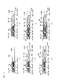
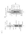
- FIG. 3 is a perspective view of an auxiliary mold body according to the present embodiment, and a cross-sectional view of the auxiliary mold body cut along a section AA.
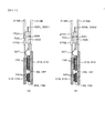
- It is a circuit diagram which shows the electric current path when an overcurrent flows into the power module which concerns on this embodiment. It is a figure explaining the temperature characteristic of the fuse material which concerns on this embodiment. It is a figure which shows the example of the shape of the fuse material which concerns on this embodiment. It is a figure which shows the 1st to 6th assembly process of the power module which concerns on this embodiment. It is a figure explaining the process of assembling the power module which concerns on this embodiment to a cooling jacket. It is an exploded perspective view of the capacitor module concerning this embodiment.
- the power conversion device 200 can be applied to a hybrid vehicle or a pure electric vehicle.
- a control configuration and a circuit configuration when applied to a hybrid vehicle are illustrated in FIGS. 1 and 2. Will be described.
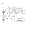
- FIG. 1 is a diagram showing a control block of a hybrid vehicle.
- the power conversion device will be described by taking as an example a vehicle drive inverter device that is used in a vehicle drive electrical system and has a very severe mounting environment and operational environment.
- the configuration of the present embodiment is optimal as a power conversion device for driving a vehicle such as an automobile or a truck.
- other power conversion devices such as a power conversion device such as a train, a ship, and an aircraft, and a factory facility are also included.
- a hybrid electric vehicle (hereinafter referred to as “HEV”) 110 is one electric vehicle, and includes two vehicle driving systems.
- One of them is an engine system that uses an engine 120 that is an internal combustion engine as a power source.
- the engine system is mainly used as a drive source for HEV.
- the other is an in-vehicle electric system using motor generators 192 and 194 as a power source.
- the in-vehicle electric system is mainly used as an HEV drive source and an HEV power generation source.
- the motor generators 192 and 194 are, for example, synchronous machines or induction machines, and operate as both a motor and a generator depending on the operation method.
- a front wheel axle 114 is rotatably supported at the front portion of the vehicle body, and a pair of front wheels 112 are provided at both ends of the front wheel axle 114.
- a rear wheel axle is rotatably supported at the rear portion of the vehicle body, and a pair of rear wheels are provided at both ends of the rear wheel axle (not shown).
- a so-called front wheel drive system is employed, but the reverse, that is, a rear wheel drive system may be employed.
- a front wheel side differential gear (hereinafter referred to as “front wheel side DEF”) 116 is provided at the center of the front wheel axle 114.
- the output shaft of the transmission 118 is mechanically connected to the input side of the front wheel side DEF 116.
- the output side of the motor generator 192 is mechanically connected to the input side of the transmission 118.
- the output side of the engine 120 and the output side of the motor generator 194 are mechanically connected to the input side of the motor generator 192 via the power distribution mechanism 122.
- the inverter units 140 and 142 are electrically connected to the battery 136 via the DC connector 138. Electric power can be exchanged between the battery 136 and the inverter units 140 and 142.
- the first motor generator unit including the motor generator 192 and the inverter unit 140 and the second motor generator unit including the motor generator 194 and the inverter unit 142 are provided, and they are selectively used according to the operation state. ing.
- the vehicle can be driven only by the power of the motor generator 192 by operating the first motor generator unit as an electric unit by the electric power of the battery 136.
- the battery 136 can be charged by generating power by operating the first motor generator unit or the second motor generator unit as the power generation unit by the power of the engine 120 or the power from the wheels.
- the battery 136 is also used as a power source for driving an auxiliary motor 195.
- the auxiliary machine is, for example, a motor that drives a compressor of an air conditioner, or a motor that drives a hydraulic pump for control.
- DC power is supplied from the battery 136 to the inverter unit 43, converted into AC power by the inverter unit 43, and supplied to the motor 195.
- the inverter unit 43 has the same function as the inverter units 140 and 142, and controls the phase, frequency, and power of alternating current supplied to the motor 195.
- the power conversion device 200 includes a capacitor module 500 for smoothing a direct current supplied to the inverter unit 140, the inverter unit 142, and the inverter unit 43.
- the inverter unit 140 will be described as a representative example.
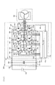
- the inverter circuit 144 is provided with three phases (U phase, V phase, W phase) corresponding to each phase winding of the armature winding of the motor generator 192 in the upper and lower arm series circuit 150.
- the upper and lower arm series circuit 150 includes an IGBT 328 (insulated gate bipolar transistor) and a diode 156 that operate as an upper arm, and an IGBT 330 and a diode 166 that operate as a lower arm.
- Each of the upper and lower arm series circuits 150 is connected to an AC power line (AC bus bar) 186 from the middle point (intermediate electrode 169) to the motor generator 192 through the AC terminal 159 and the AC connector 188.
- the collector electrode 153 of the IGBT 328 of the upper arm is connected to the capacitor electrode on the positive side of the capacitor module 500 via the positive terminal (P terminal) 157, and the emitter electrode of the IGBT 330 of the lower arm is connected to the capacitor via the negative terminal (N terminal) 158.
- the module 500 is electrically connected to the capacitor electrode on the negative electrode side.
- the control unit 170 includes a driver circuit 174 that drives and controls the inverter circuit 144 and a control circuit 172 that supplies a control signal to the driver circuit 174 via the signal line 176.
- the IGBT 328 and the IGBT 330 operate in response to the drive signal output from the control unit 170, and convert DC power supplied from the battery 136 into three-phase AC power. The converted electric power is supplied to the armature winding of the motor generator 192.
- the IGBT 328 includes a collector electrode 153, a signal emitter electrode 155, and a gate electrode 154.
- the IGBT 330 includes a collector electrode 163, a signal emitter electrode 165, and a gate electrode 164.
- a diode 156 is electrically connected between the collector electrode 153 and the emitter electrode.
- a diode 166 is electrically connected between the collector electrode 163 and the emitter electrode.
- a MOSFET metal oxide semiconductor field effect transistor
- the capacitor module 500 is electrically connected to the battery 136 through a positive capacitor terminal 506, a negative capacitor terminal 504, and a DC connector 138. Note that the inverter unit 140 is connected to the positive capacitor terminal 506 via the DC positive terminal 314 and is connected to the negative capacitor terminal 504 via the DC negative terminal 316.
- the control circuit 172 includes a microcomputer (hereinafter referred to as “microcomputer”) for performing arithmetic processing on the switching timing of the IGBT 328 and the IGBT 330.
- the microcomputer receives as input information a target torque value required for the motor generator 192, a current value supplied to the armature winding of the motor generator 192 from the upper and lower arm series circuit 150, and a magnetic pole of the rotor of the motor generator 192. The position has been entered.
- the target torque value is based on a command signal output from a host controller (not shown).
- the current value is detected based on the detection signal output from the current sensor 180 via the signal line 182.
- the magnetic pole position is detected based on a detection signal output from a rotating magnetic pole sensor (not shown) provided in the motor generator 192.
- a rotating magnetic pole sensor not shown
- the case where the current values of three phases are detected will be described as an example, but the current values for two phases may be detected.
- the microcomputer in the control circuit 172 calculates the d and q axis current command values of the motor generator 192 based on the target torque value, and the calculated d and q axis current command values and the detected d and q
- the voltage command values for the d and q axes are calculated based on the difference from the current value of the shaft, and the calculated voltage command values for the d and q axes are calculated based on the detected magnetic pole position. Convert to W phase voltage command value.
- the microcomputer generates a pulse-like modulated wave based on the comparison between the fundamental wave (sine wave) and the carrier wave (triangular wave) based on the voltage command values of the U-phase, V-phase, and W-phase, and the generated modulation
- the wave is output to the driver circuit 174 via the signal line 176 as a PWM (pulse width modulation) signal.
- the driver circuit 174 When driving the lower arm, the driver circuit 174 outputs a drive signal obtained by amplifying the PWM signal to the gate electrode of the corresponding IGBT 330 of the lower arm. Further, when driving the upper arm, the driver circuit 174 amplifies the PWM signal after shifting the level of the reference potential of the PWM signal to the level of the reference potential of the upper arm, and uses this as a drive signal as a corresponding upper arm. Are output to the gate electrodes of the IGBTs 328 respectively.
- control unit 170 performs abnormality detection (overcurrent, overvoltage, overtemperature, etc.) to protect the upper and lower arm series circuit 150. For this reason, sensing information is input to the control unit 170. For example, information on the current flowing through the emitter electrodes of the IGBTs 328 and IGBTs 330 is input from the signal emitter electrode 155 and the signal emitter electrode 165 of each arm to the corresponding drive unit (IC). Thereby, each drive part (IC) detects an overcurrent, and when an overcurrent is detected, the switching operation of the corresponding IGBT 328 and IGBT 330 is stopped, and the corresponding IGBT 328 and IGBT 330 are protected from the overcurrent.
- abnormality detection overcurrent, overvoltage, overtemperature, etc.
- Information on the temperature of the upper and lower arm series circuit 150 is input to the microcomputer from a temperature sensor (not shown) provided in the upper and lower arm series circuit 150.
- voltage information on the DC positive side of the upper and lower arm series circuit 150 is input to the microcomputer.
- the microcomputer performs over-temperature detection and over-voltage detection based on the information, and stops switching operations of all the IGBTs 328 and IGBTs 330 when an over-temperature or over-voltage is detected.
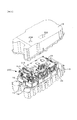
- FIG. 3 is an exploded perspective view for explaining an installation place of the power conversion device 200 according to the present embodiment.
- the power conversion device 200 is fixed to an aluminum casing 119 for housing the transmission 118. Since the power converter 200 has a substantially rectangular shape on the bottom and top surfaces, it can be easily attached to the vehicle and can be easily produced.
- the cooling jacket 12 holds a power module 300 and a capacitor module 500, which will be described later, and is cooled by a cooling medium.
- the cooling jacket 12 is fixed to the housing 119, and an inlet pipe 13 and an outlet pipe 14 are formed on a surface facing the housing 119. By connecting the inlet pipe 13 and the outlet pipe 14 with the pipe formed in the housing 119, a cooling medium for cooling the transmission 118 flows into and out of the cooling jacket 12.
- the case 10 covers the power conversion device 200 and is fixed to the housing 119 side.
- the bottom of the case 10 is configured to face the control circuit board 20 on which the control circuit 172 is mounted.
- a first opening 202 and a second opening 204 that are connected to the outside from the bottom of the case 10 are formed on the bottom surface of the case 10.
- the connector 21 is connected to the control circuit board 20 and transmits various signals from the outside to the control circuit board 20.
- the battery negative electrode side connection terminal portion 510 and the battery positive electrode side connection terminal portion 512 electrically connect the battery 136 and the capacitor module 500.
- Connector 21, battery negative electrode side connection terminal portion 510, and battery positive electrode side connection terminal portion 512 are extended toward the bottom surface of case 10, connector 21 projects from first opening 202, and battery negative electrode side connection terminal portion 510.
- the battery positive electrode side connection terminal portion 512 protrudes from the second opening 204.
- the case 10 is provided with a seal member (not shown) around the first opening 202 and the second opening 204 on the inner wall thereof.
- the direction of the mating surface of the terminal of the connector 21 and the like varies depending on the vehicle type. However, especially when trying to mount on a small vehicle, the mating surface is directed upward from the viewpoint of the size restriction in the engine room and the assembling property. It is preferable to take out.
- the power conversion device 200 is disposed above the transmission 118 as in the present embodiment, the workability is improved by projecting toward the opposite side of the transmission 118.
- the connector 21 needs to be sealed from the outside atmosphere.
- the case 10 is assembled to the connector 21 from above, so that when the case 10 is assembled to the housing 119, the seal member that contacts the case 10 attaches the connector 21. It can be pressed to improve airtightness.
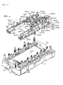
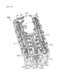
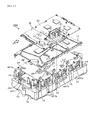
- FIG. 4 is a perspective view in which the entire configuration of the power conversion device according to the present embodiment is disassembled into components.
- the cooling jacket 12 is provided with a flow path 19 (FIG. 5).
- a flow path 19 (FIG. 5).
- openings 400a to 400c are formed along the refrigerant flow direction 418, and the openings 402a to 402c are formed. It is formed along the flow direction 422 of the refrigerant.
- the openings 400a to 400c are closed by the power modules 300a to 300c, and the openings 402a to 402c are closed by the power modules 301a to 301c.
- a storage space 405 for storing the capacitor module 500 is formed in the cooling jacket 12.
- the capacitor module 500 is cooled by the refrigerant flowing in the flow path 19. Since the capacitor module 500 is sandwiched between the flow path 19 for forming the refrigerant flow direction 418 and the flow path 19 for forming the refrigerant flow direction 422, the capacitor module 500 can be efficiently cooled.
- the cooling jacket 12 is formed with a protrusion 407 at a position facing the inlet pipe 13 and the outlet pipe 14.
- the protrusion 407 is formed integrally with the cooling jacket 12.
- the auxiliary power module 350 is fixed to the protruding portion 407 and is cooled by the refrigerant flowing in the flow path 19.
- a bus bar module 800 is disposed on the side of the auxiliary power module 350.
- the bus bar module 800 includes an AC bus bar 186, a current sensor 180, and the like, details of which will be described later.
- the storage space 405 of the capacitor module 500 is provided in the center of the cooling jacket 12, and the flow paths 19 are provided so as to sandwich the storage space 405.
- the power modules 300a to 300c for driving the vehicle and The power modules 301a to 301c are disposed, and the auxiliary power module 350 is disposed on the upper surface of the cooling jacket 12.
- the main structure of the flow path 19 of the cooling jacket 12 integrally with the cooling jacket 12 by casting an aluminum material, the flow path 19 has the effect of increasing the mechanical strength in addition to the cooling effect.
- the cooling jacket 12 and the flow path 19 become an integral structure by making it by aluminum casting, heat conduction improves, and cooling efficiency improves.
- the power module 300a to 300c and the power module 301a to 301c are fixed to the flow path 19 to complete the flow path 19, and a water leak test is performed.
- the work of attaching the capacitor module 500, the auxiliary power module 350, and the substrate can be performed next.
- the cooling jacket 12 is disposed at the bottom of the power conversion device 200, and then the work of fixing necessary components such as the capacitor module 500, the auxiliary power module 350, the bus bar module 800, and the board can be sequentially performed from the top. As a result, productivity and reliability are improved.
- the driver circuit board 22 is disposed above the auxiliary power module 350 and the bus bar module 800.
- the metal base plate 11 is disposed between the driver circuit board 22 and the control circuit board 20.
- the metal base plate 11 functions as an electromagnetic shield for a circuit group mounted on the driver circuit board 22 and the control circuit board 20, and also releases and cools heat generated by the driver circuit board 22 and the control circuit board 20. Have.
- FIG. 5 is a bottom view of the cooling jacket 12 having the flow path 19.
- the cooling jacket 12 and the flow path 19 provided inside the cooling jacket 12 are integrally cast.
- An opening 404 connected to one is formed on the lower surface of the cooling jacket 12.
- the opening 404 is closed by a lower cover 420 having an opening at the center.
- a seal member 409a and a seal member 409b are provided between the lower cover 420 and the cooling jacket 12 to maintain airtightness.
- an inlet hole 401 for inserting the inlet pipe 13 and an outlet hole 403 for inserting the outlet pipe 14 are formed in the vicinity of one end side and along the side edge.
- the lower cover 420 is formed with a convex portion 406 that protrudes in the arrangement direction of the transmission 118.
- the convex portion 406 is provided for each of the power modules 300a to 300c and the power modules 301a to 301c.
- the refrigerant flows through the inlet hole 401 toward the first flow path portion 19a formed along the short side of the cooling jacket 12. Then, the refrigerant flows through the second flow path portion 19b formed along the longitudinal side of the cooling jacket 12 as in the flow direction 418. Further, the refrigerant flows through the third flow path portion 19 c formed along the short side of the cooling jacket 12 as in the flow direction 421. The third flow path portion 19c forms a folded flow path. Further, the refrigerant flows through the fourth flow path portion 19d formed along the longitudinal side of the cooling jacket 12 as in the flow direction 422. The fourth flow path portion 19d is provided at a position facing the second flow path portion 19b with the capacitor module 500 interposed therebetween. Further, the refrigerant flows out to the outlet pipe 14 through the fifth flow path portion 19 e and the outlet hole 403 formed along the short side of the cooling jacket 12 as in the flow direction 423.
- the first flow path portion 19a, the second flow path portion 19b, the third flow path portion 19c, the fourth flow path portion 19d, and the fifth flow path portion 19e are all formed larger in the depth direction than in the width direction.
- the power modules 300a to 300c are inserted from the openings 400a to 400c formed on the upper surface side of the cooling jacket 12 (see FIG. 4) and stored in the storage space in the second flow path portion 19b.
- An intermediate member 408a is formed between the storage space of the power module 300a and the storage space of the power module 300b so as not to stagnate the refrigerant flow.
- an intermediate member 408b is formed between the storage space of the power module 300b and the storage space of the power module 300c so as not to stagnate the refrigerant flow.
- the intermediate member 408a and the intermediate member 408b are formed such that their main surfaces are along the flow direction of the refrigerant.
- the fourth flow path portion 19d forms a storage space and an intermediate member for the power modules 301a to 301c.
- the cooling jacket 12 is formed so that the opening 404 and the openings 400a to 400c and 402a to 402c face each other, the cooling jacket 12 is configured to be easily manufactured by aluminum casting.
- the lower cover 420 is provided with a support portion 410a and a support portion 410b for contacting the casing 119 and supporting the power conversion device 200.
- the support portion 410 a is provided close to one end side of the lower cover 420, and the support portion 410 b is provided close to the other end side of the lower cover 420.
- power conversion device 200 can be firmly fixed to the side wall of casing 119 formed in accordance with the cylindrical shape of transmission 118 or motor generator 192.
- the support portion 410b is configured to support the resistor 450.
- the resistor 450 is for discharging electric charges charged in the capacitor cell in consideration of occupant protection and safety during maintenance.
- the resistor 450 is configured to continuously discharge high-voltage electricity. However, in the unlikely event that there is any abnormality in the resistor or discharge mechanism, consideration was given to minimize damage to the vehicle. Must be configured. In other words, when the resistor 450 is arranged around the power module, the capacitor module, the driver circuit board, etc., there is a possibility that the resistor 450 may spread near the main component in the event that the resistor 450 has a problem such as heat generation or ignition. Conceivable.
- the power modules 300a to 300c, the power modules 301a to 301c, and the capacitor module 500 are disposed on the opposite side of the casing 119 housing the transmission 118 with the cooling jacket 12 interposed therebetween, and the resistor 450 Is disposed in a space between the cooling jacket 12 and the housing 119. Accordingly, the resistor 450 is disposed in a closed space surrounded by the cooling jacket 12 and the casing 119 formed of metal. Note that the electric charge stored in the capacitor cell in the capacitor module 500 is a resistor through a wiring passing through the side of the cooling jacket 12 by the switching operation of the switching means mounted on the driver circuit board 22 shown in FIG. The discharge is controlled to 450.
- the switching is controlled so as to discharge at high speed. Since the cooling jacket 12 is provided between the driver circuit board 22 that controls the discharge and the resistor 450, the driver circuit board 22 can be protected from the resistor 450. Further, since the resistor 450 is fixed to the lower cover 420, the resistor 450 is provided at a position that is thermally close to the flow path 19, so that abnormal heat generation of the resistor 450 can be suppressed.
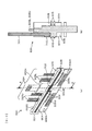
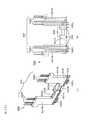
- FIG. 6A is a perspective view of the power module 300a of the present embodiment.
- FIG. 6B is a cross-sectional view of the power module 300a of the present embodiment.
- the power semiconductor elements (IGBT 328, IGBT 330, diode 156, and diode 166) constituting the upper and lower arm series circuit are connected by the conductor plate 315 and the conductor plate 318, or by the conductor plate 316 and the conductor plate 319, as shown in FIGS. It is fixed by being sandwiched from both sides.
- These conductor plates are assembled with an auxiliary molded body 600 formed by integrally molding the signal wirings which are the external signal terminals 325U and the external signal terminals 325L.
- the conductor plate 315 and the like are sealed with the first sealing resin 348 with the heat dissipation surface exposed, and the insulating sheet 333 is thermocompression bonded to the heat dissipation surface.
- the module primary sealing body 302 sealed with the first sealing resin 348 is inserted into the module case 304 and sandwiched with the insulating sheet 333, and is thermocompression bonded to the inner surface of the module case 304 that is a CAN type cooler.
- the CAN-type cooler is a cylindrical cooler having an insertion port 306 on one surface and a bottom on the other surface.
- the module case 304 is made of an aluminum alloy material such as Al, AlSi, AlSiC, Al—C, etc., and is integrally formed without a joint.
- the material used for the module case 304 is specifically an aluminum alloy material, but it is also possible to use copper or a copper alloy material. When a copper material is used, the module case 304 can be produced at a lower cost than when an aluminum alloy material is used.
- the module case 304 has a structure in which no opening other than the insertion port 306 is provided. The insertion port 306 is surrounded by a flange 304B. Further, as shown in FIG.
- the first heat radiating surface 307A and the second heat radiating surface 307B which are wider than the other surfaces, are arranged facing each other, and the opposing first heat radiating surface 307A and The three surfaces connecting the second heat radiating surface 307B constitute a surface sealed with a width narrower than the first heat radiating surface 307A and the second heat radiating surface 307B, and the insertion port 306 is formed on the surface of the other side.
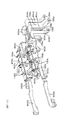
- a fuse material 700 is disposed in the vicinity of the auxiliary mold body 600 protruding from the insertion port 306. By providing the fuse material 700, it is possible to prevent the power module from being destroyed by an overcurrent.
- the module case 304 is directly inserted into the water channel through the insertion ports 400a, 400b, and 400c, and the outer surface of the module case 304 is in direct contact with the cooling medium. If the fuse material 700 is disposed inside the module case 304, the module case 304 may be destroyed when the fuse material 700 is melted, and the entire device may be destroyed due to water leakage. Therefore, as in the present embodiment, the fuse material 700 is provided on the auxiliary mold body 600 in which the fuse material 700 protrudes from the insertion port 306. Thereby, even when the fuse material 700 is melted, the module case 304 can be prevented from being broken, and the reliability is improved.
- the fuse material 700 is provided in the vicinity of the module case in direct contact with the refrigerant, and is further connected to the DC negative electrode wiring 319A and the DC negative electrode terminal 319B.
- One surface of the DC negative electrode wiring 319A is connected to the IGBTs 328 and 330 and the diodes 156 and 166, and the other surface is bonded to the first heat dissipation surface 307A via a resin insulating layer.
- the fuse material 700 connected to the DC negative electrode wiring 319A and the DC negative electrode terminal 319B is also cooled to prevent heat generation due to a noise voltage or the like of the fuse material 700 during normal operation, and thus the fuse material 700 is blown during normal operation. Therefore, reliability can be improved. Further, even when an overcurrent actually occurs, the heat generation of the semiconductor element is directly transmitted to the fuse material 700 by the above configuration, and the temperature of the fuse material 700 can follow the temperature of the semiconductor element. The fuse material 700 can be surely blown before being destroyed. As a result, the reliability is improved.
- the shape of the module case 304 does not have to be an accurate rectangular parallelepiped, and the corners may form a curved surface as shown in FIG.
- the metallic case having such a shape By using the metallic case having such a shape, even when the module case 304 is inserted into the flow path 19 through which a coolant such as water or oil flows, a seal against the coolant can be secured by the flange 304B. Can be prevented from entering the inside of the module case 304 with a simple configuration.
- the flange 304B By forming the flange 304B at the periphery of the insertion port 306, the heat generated by the fuse material 700 is directly conducted to the sealing materials 1000 and 1001 (shown in FIG. 15) between the flange 304B and the water channel forming body. Therefore, leakage due to melting of the sealing materials 1000 and 1001 can be prevented, and reliability is improved.
- the fins 305 are uniformly formed on the first heat radiation surface 307A and the second heat radiation surface 307B facing each other. Further, a curved portion 304A having an extremely thin thickness is formed on the outer periphery of the first heat radiating surface 307A and the second heat radiating surface 307B. Since the curved portion 304A is extremely thin to such an extent that it can be easily deformed by pressurizing the fin 305, the productivity after the module primary sealing body 302 is inserted is improved.
- the gap remaining inside the module case 304 is filled with the second sealing resin 351. Further, as shown in FIGS. 8 and 9, a DC positive electrode wiring 315A and a DC negative electrode wiring 319A for electrical connection with the capacitor module 500 are provided, and a DC positive electrode terminal 315B and a DC negative electrode are provided at the tip thereof. A terminal 319B is formed. An AC wiring 320 for supplying AC power to the motor generator 192 or 194 is provided, and an AC terminal 321 is formed at the tip thereof.
- the DC positive electrode wiring 315A is formed integrally with the conductor plate 315
- the AC wiring 320 is formed integrally with the conductor plate 316.
- the DC negative electrode wiring 319A is formed separately from the DC negative electrode terminal 319B.
- the DC negative electrode wiring 319 ⁇ / b> A side of the DC negative electrode terminal 319 ⁇ / b> B is exposed from the auxiliary mold body 600 and forms an exposed portion 702.
- the DC negative electrode terminal side of the DC negative electrode wiring 319 ⁇ / b> A is also exposed from the auxiliary mold body 600 to form an exposed portion 703.
- One end of the fuse material 700 is connected to the exposed portion 702, the other end is connected to the exposed portion 703, and the DC negative electrode wiring 319A and the DC negative electrode terminal 319B are connected.
- the auxiliary mold body 600 When the DC negative electrode wiring 319A and the DC negative electrode terminal 319B are fixed to the auxiliary mold body 600, a special fixing jig is required when the fuse material 700 is welded to the exposed portion 702 and the exposed portion 703 by ultrasonic welding or the like. This improves productivity. Further, when the fuse material 700 is welded by ultrasonic welding or the like, the auxiliary mold body 600 can be subjected to stress instead of the base, so that the fuse material 700 can be assembled with high reliability.
- the gap between the conductor plate and the inner wall of the module case 304 can be reduced, and the power semiconductor element The generated heat can be efficiently transmitted to the fins 305.
- the generation of thermal stress can be absorbed by the insulating sheet 333, so that the insulating sheet 333 is suitable for use in a power converter for a vehicle having a large temperature change.
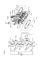
- FIG. 7A is an internal cross-sectional view in which the module case 304, the insulating sheet 333, the first sealing resin 348, and the second sealing resin 351 are removed in order to help understanding.
- FIG. 7B is an internal perspective view.
- FIG. 8A is an exploded view for helping understanding of the structure of FIG.
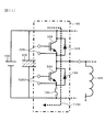
- FIG. 8B is a circuit diagram of the power module 300.
- FIG. 9A is a circuit diagram for explaining an inductance reduction effect
- FIG. 9B is a perspective view showing a current flow for explaining an inductance reduction effect.
- the direct current positive electrode side conductor plate 315 and the alternating current output side conductor plate 316 are arranged in substantially the same plane.
- the collector electrode of the IGBT 328 on the upper arm side and the cathode electrode of the diode 156 on the upper arm side are fixed.
- the collector electrode of the IGBT 330 on the lower arm side and the cathode electrode of the diode 166 on the lower arm side are fixed.
- the AC conductor plate 318 and the conductor plate 319 are arranged in substantially the same plane.
- the emitter electrode of the IGBT 328 on the upper arm side and the anode electrode of the diode 156 on the upper arm side are fixed.
- an emitter electrode of the IGBT 330 on the lower arm side and an anode electrode of the diode 166 on the lower arm side are fixed.
- Each power semiconductor element is fixed to an element fixing portion 322 provided on each conductor plate via a metal bonding material 160.
- the metal bonding material 160 is, for example, a low-temperature sintered bonding material including a solder material, a silver sheet, and fine metal particles.
- Each power semiconductor element has a flat plate-like structure, and each electrode of the power semiconductor element is formed on the front and back surfaces. As shown in FIG. 7A, each electrode of the power semiconductor element is sandwiched between the conductor plate 315 and the conductor plate 318, or the conductor plate 316 and the conductor plate 319. In other words, the conductor plate 315 and the conductor plate 318 are stacked so as to face each other substantially in parallel via the IGBT 328 and the diode 156. Similarly, the conductor plate 316 and the conductor plate 319 have a stacked arrangement facing each other substantially in parallel via the IGBT 330 and the diode 166. Further, the conductor plate 316 and the conductor plate 318 are connected via an intermediate electrode 329. By this connection, the upper arm circuit and the lower arm circuit are electrically connected to form an upper and lower arm series circuit.
- the direct current positive electrode wiring 315A and the direct current negative electrode wiring 319A have a shape extending substantially in parallel while facing each other through an auxiliary mold body 600 formed of a resin material.
- the external signal terminal 325U and the external signal terminal 325L are formed integrally with the auxiliary mold body 600 and extend in the same direction as the DC positive electrode wiring 315A and the DC negative electrode wiring 319A.
- a thermosetting resin having an insulating property or a thermoplastic resin is suitable. Thereby, insulation between the DC positive electrode wiring 315A, the DC negative electrode wiring 319A, the external signal terminal 325U, and the external signal terminal 325L can be secured, and high-density wiring is possible.
- the direct current positive electrode wiring 315A and the direct current negative electrode wiring 319A are arranged so as to face each other substantially in parallel, so that currents that instantaneously flow during the switching operation of the power semiconductor element face each other in the opposite direction. As a result, the magnetic fields produced by the currents cancel each other out, and this action can reduce the inductance.
- FIG. 9A it is assumed that the diode 166 on the lower arm side is conducting in the forward bias state.
- the diode 166 on the lower arm side is reversely biased, and a recovery current caused by carrier movement passes through the upper and lower arms.
- a recovery current 360 shown in FIG. 9B flows through each of the conductor plates 315, 316, 318, and 319.
- the recovery current 360 passes through the DC positive terminal 315B disposed opposite to the DC negative terminal 319B, and then flows through a loop-shaped path formed by the conductor plates 315, 316, 318, and 319.
- the current flows again as shown by the solid line through the DC negative terminal 319B disposed opposite to the DC positive terminal 315B.
- an eddy current 361 flows through the first heat radiating surface 307A and the second heat radiating surface 307B of the module case 304. Due to the magnetic field canceling effect generated by the equivalent circuit 362 in the current path of the eddy current 361, the wiring inductance 363 in the loop-shaped path is reduced.
- the loop-shaped current path flows along a path close to the DC positive terminal 315B side of the conductor plate 315 and passes through the IGBT 328 and the diode 156 as indicated by a dotted line.
- the loop-shaped current path flows through a path farther from the DC positive terminal 315B side of the conductor plate 318, as shown by a solid line, and then flows through a path farther from the DC positive terminal 315B side of the conductor plate 316, as shown by a dotted line. It passes through the diode 166.
- the loop-shaped current path flows along a path close to the DC negative electrode wiring 319A side of the conductor plate 319.
- a current path closer to the loop shape is formed by passing the loop-shaped current path closer to or farther from the DC positive terminal 315B and the DC negative terminal 319B.
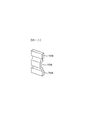
- FIG. 10 (a) is a perspective view of the auxiliary mold body 600
- FIG. 10 (b) is a cross-sectional view taken along the line AA of FIG. 10 (a).
- the auxiliary mold body 600 has the signal conductor 324 integrated by insert molding.
- the signal conductor 324 receives the temperature information of the upper arm side gate electrode terminal 154 and the emitter electrode terminal 155, the upper arm side gate electrode terminal 164 and the emitter electrode terminal 165 (see FIG. 2), and the power semiconductor element.
- a terminal for transmission is included. In the description of this embodiment, these terminals are collectively referred to as external signal terminals 325U and 325L.
- the signal conductor 324 forms the external signal terminals 325U and 325L at one end and the element side signal terminals 326U and 326L at the other end.
- the element-side signal terminals 326U and 326L are connected to signal pads provided on the surface electrode of the power semiconductor element by, for example, wires.
- the sealing portion 601 has a shape extending in a direction crossing the major axis of the shape of the DC positive electrode wiring 315A, the DC negative electrode wiring 319A, or the AC wiring 320 shown in FIG.
- the auxiliary mold body 600 is formed so that its length is longer than the entire length of the conductor plates 315 and 316 arranged side by side or the entire length of the conductor plates 319 and 320 arranged side by side. That is, the lengths of the conductor plates 315 and 316 arranged side by side or the lengths of the conductor plates 319 and 320 arranged side by side are within the range of the lateral length of the auxiliary mold body 600.
- the sealing portion 601 has a hollow shape and forms a wiring fitting portion 602B for fitting the DC negative electrode wiring 319A in the hollow.
- the sealing portion 601 has a hollow shape and forms a wiring fitting portion 602A for fitting the DC positive electrode wiring 315A into the hollow.
- the sealing portion 601 is disposed on the side portion of the wiring fitting portion 602A, has a hollow shape, and further forms a wiring fitting portion 602C for fitting the AC wiring 320 into the hollow.
- Each wiring is positioned by fitting each wiring to these wiring fitting portions 602A to 602C. Thereby, it becomes possible to perform the filling operation of the resin sealing material after firmly fixing each wiring, and the mass productivity is improved.
- the sealing portion 601 is formed with a mold pressing surface 604 that comes into contact with a mold used for resin sealing, and the mold pressing surface 604 prevents resin leakage during resin sealing.
- a protrusion 605 is formed around the outer periphery of the sealing portion 601 in the longitudinal direction. A plurality of protrusions 605 are provided to enhance the resin leakage prevention effect. Further, since the protrusions 605 are also provided in the wiring fitting part 602A and the wiring fitting part 602B, it is possible to prevent the resin sealing material from leaking from around the DC positive electrode wiring 315A and the DC negative electrode wiring 319A.
- thermoplastic liquid crystal polymer or polybutylene terephthalate high heat resistance
- PBT polybutylene terephthalate
- PPS polyphenylene sulfide resin
- a plurality of through holes 606A are provided in the longitudinal direction on the side of the power semiconductor element in the short direction of the sealing portion 601.
- the auxiliary mold body 600 supporting each wiring is inserted into a mold preheated to about 150 to 180 ° C.
- the auxiliary mold body 600, the DC positive electrode wiring 315A, the DC negative electrode wiring 319A, the AC wiring 320, the conductor plate 315, the conductor plate 316, the conductor plate 318, and the conductor plate 319 are firmly connected to each other.
- FIG. 11 shows a current path when an overcurrent 1100 flows in the circuit. In this way, even if the DC circuit 150 breaks down and an overcurrent 1100 flows between the batteries 136, the overcurrent before the first sealing resin 348 is decomposed or melted by the heat generated from the power semiconductor element. Can be cut off.
- the temperature characteristics of the fuse material 700 will be described in detail with reference to FIG.
- the horizontal axis in FIG. 12 is the time when the overcurrent flows in the circuit, and the vertical axis is the temperature corresponding to the time when the overcurrent flows.
- 900 is the sealing resin temperature
- 901 is the fuse material temperature.
- the overcurrent 1100 when the IGBT upper and lower arms are short-circuited is a large current of 7000 to 10000 A.
- the overcurrent 1100 is cut off in a short time within about 10 usec by the short circuit protection function of the driver circuit 174.
- the sealing resin temperature 900 near the IGBT chip rises to 200 to 300 ° C. at 100 usec.
- the temperature of the fuse material 700 also rises in proportion, and rises at the same temperature as the sealing resin temperature 900 near the IGBT chip or faster than the sealing resin temperature 900.
- the serious destruction of the sealed power module is considered to be caused by the accumulation of gas inside the module case due to gas decomposition of the first sealing resin 348 due to overheating. Therefore, by setting the fuse fusing temperature 902 to the same level as or lower than the gas decomposition start temperature 903 of the sealing resin, the overcurrent 1100 can be interrupted reliably and with minimal internal gas generation.
- the gas decomposition start temperature 903 of the sealing resin ranges from about 300 ° C. to 350 ° C. or more in the case of a flame retardant material.
- the auxiliary mold body 600 and the sealing resin 601 are preferably heat-resistant thermoplastic resins such as polybutylene terephthalate (PBT) and polyphenylene sulfide resin (PPS) from the functional aspect during transfer molding.
- PBT polybutylene terephthalate
- PPS polyphenylene sulfide resin
- These gas decomposition temperatures are often higher than the gas decomposition start temperature 903 of the sealing resin, and there are series from 340 to 500 ° C.
- the fuse fusing temperature 902 is surely lower than the gas decomposition temperature of the auxiliary mold body 600, so that a serious breakdown chain due to dielectric breakdown between the DC positive electrode conductor plate 315 and the DC positive electrode negative electrode plate 319 is obtained. Can be prevented.
- the fuse material 700 As the material of the fuse material 700, an Al alloy (Al-Si system, Al-Si-Mg), an Sn alloy (Sn-Cu system, Sn-Zn system, Sn-In system, Sn-Bi system, Sn-Cd system) ) Etc., and a lead-free alloy is desirable. Further, when an Sn alloy is used for the fuse material 700, metal bonding by ultrasonic welding becomes difficult. Therefore, as shown in FIG. 13, the fuse fusing part 705 is made of Sn alloy and the fuse joining part 706 is made of Cu alloy. Alternatively, it may be composed of an Al alloy. Both can be joined by brazing or caulking.
- the assembly process of the power module will be described with reference to FIGS. 14 (a) to 14 (f).
- the IGBTs 328 and 330 and the diodes 156 and 158 are mounted on the conductor plate 315 and the conductor plate 316 connected to the DC positive terminal 315B as shown in FIG.
- the conductor plate 319 and the conductor plate 318 are joined to the IGBTs 328 and 330 and the diodes 156 and 158.
- the auxiliary mold body 600 is inserted between the DC positive electrode wiring 315A and the DC negative electrode wiring 319A to position the DC positive electrode wiring 315A and the DC negative electrode wiring 319A. Fixed.
- the signal conductor 324 and the gate electrodes of the IGBTs 328 and 330 are joined by wire bonding 327.
- the fourth step shown in FIG. 14 (d) is a step of performing a so-called transfer mold in which the power module assembled as shown in FIG. 14 (c) is sealed with a resin material.
- the fifth step is a step of assembling the fuse material 700 as shown in FIG.
- the resin insulating layer 333 is bonded to both surfaces of the transfer-molded power module.
- the fuse material 700 may be formed by separately forming the DC positive electrode wiring 315A and the DC positive electrode terminal 315B on the positive electrode side, or on both the positive electrode side and the negative electrode side, but the fuse material 700 is provided only on the negative electrode side. Therefore, productivity is improved because the assembly is performed so that the positive electrode side faces down throughout the entire process.
- the reason for assembling so that the positive electrode side is down throughout the entire process is due to the structure of the IGBT.
- the gate electrode is formed on the emitter side of the IGBT.
- the IGBT is bonded from the emitter side by solder, and the IGBT and metal conductor are bonded from the IGBT collector side than by soldering. And the joint area becomes smaller. For this reason, when stress is applied in the assembly process, the IGBT or the like is peeled off, or the IGBT itself is displaced from the assembled position.
- the bonding area between the IGBT and the metal conductor is increased by always bonding the positive electrode side downward, that is, by joining from the collector side of the IGBT with solder. Therefore, when stress is applied in the assembling process, the semiconductor element such as the IGBT is not easily peeled off, and the IGBT is not easily displaced, so that the reliability of the power module is improved.
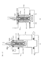
- FIG. 15 is a diagram illustrating a process of assembling the power module 300 to the water cooling jacket 12 of the power converter.
- the water cooling jacket 12 is a cooling unit in which a flow path 19 through which a cooling medium flows is formed.
- the cooling jacket 12 has an opening in the upper portion thereof, and an opening is formed on the side facing the opening.
- the power module 300 is inserted from the opening, and leakage of the refrigerant is prevented by the seal 1000 and the flange 304B of the module case 304.
- water is used as the refrigerant.
- the upper arm circuit sandwiched between the conductor plates 315 and 318 and the lower arm circuit sandwiched between the conductor plates 316 and 319 are arranged side by side along the direction of the refrigerant flow.
- the module can be made smaller. Moreover, it becomes thin in thickness and the fluid resistance with respect to the flow of a refrigerant
- coolant is suppressed.
- the upper arm circuit or the lower arm circuit is made of two power semiconductor elements connected in parallel, and the two power semiconductor elements connected in parallel are connected between the conductor plates 315 and 318 or the above-mentioned power semiconductor elements. Between the conductor plates 316 and 319, they are arranged side by side in the direction along the flow of the refrigerant, and this structure makes the entire module smaller.
- the power module 300 includes a module primary sealing body 302 (shown in FIG. 6B) having a built-in upper and lower arm circuit and a resin insulating layer 333 that are completely closed without a joint.
- a module primary sealing body 302 shown in FIG. 6B
- the built-in upper and lower arm circuits and the resin insulating layer 333 can be protected from penetration of the cooling medium.
- heat generated during operation of the power semiconductor element is diffused from both sides with a conductor plate and transmitted to the insulating sheet 333, and heat is radiated from the heat radiation surfaces 307A and 307B of the module case 304 and the fins 305, thereby realizing high cooling performance. It is a highly reliable structure capable of high current density.
- An auxiliary mold body 600 made of an insulating resin material is interposed between the DC positive electrode wiring 315A and the DC negative electrode wiring 319A so as to be fitted together, and the DC positive electrode wiring 315A and the DC negative electrode wiring are secured while ensuring insulation.
- 319A can be arranged substantially parallel to each other on the basis of high reliability. For this reason, insulation reliability can be ensured and inductance can be reduced, the power converter can be adapted to high-speed switching operation, the degree of control freedom is increased, and a good current balance is obtained. As a result, the power modules 300 can be connected in parallel, and a power conversion device having an increased current capacity can be realized.
- the fuse material 700 is melted, so that the overcurrent 800 is cut off, and the gas decomposition of the sealing resin can be prevented from proceeding at the temperature inside the power module 300, and the module case 304 and the water channel jacket 19A. Since fusing occurs outside, there is no risk of water leakage, and stable and serious destruction can be prevented.
- FIG. 16 is an exploded perspective view of the capacitor module 500 of the present embodiment.
- the laminated conductor plate 501 is composed of a negative electrode conductor plate 505 and a positive electrode conductor plate 507 formed of a thin plate-like wide conductor, and further an insulating sheet 517 sandwiched between the negative electrode conductor plate 505 and the positive electrode conductor plate 507. Low inductance is achieved.
- the laminated conductor plate 501 has a substantially rectangular shape.
- the battery positive terminal 508 and the battery negative terminal 509 are formed in a state where they are raised from one side of the laminated conductor plate 501 in the short direction.
- the capacitor terminals 503a to 503c are formed in a state where they are raised from one side in the longitudinal direction of the laminated conductor plate 501.
- the capacitor terminals 503d to 503f are formed in a state where they are raised from the other side in the longitudinal direction of the laminated conductor plate 501.
- the capacitor terminals 503a to 503f are raised in a direction crossing the main surface of the laminated conductor plate 501.
- Capacitor terminals 503a to 503c are connected to power modules 300a to 300c, respectively.
- Capacitor terminals 503d to 503f are connected to power modules 301a to 301c, respectively.
- a part of the insulating sheet 517 is provided between the negative-side capacitor terminal 504a and the positive-side capacitor terminal 506a constituting the capacitor terminal 503a to ensure insulation.
- the negative electrode conductor plate 505, the positive electrode conductor plate 507, the battery positive electrode side terminal 508, the battery negative electrode side terminal 509, and the capacitor terminals 503a to 503f are configured by integrally formed metal plates to reduce inductance. And improve productivity.
- a plurality of capacitor cells 514 are provided below the laminated conductor plate 501.
- eight capacitor cells 514 are arranged in a line along one side in the longitudinal direction of the multilayer conductor plate 501, and another eight capacitor cells 514 are arranged on the other side in the longitudinal direction of the multilayer conductor plate 501.
- a total of 16 capacitor cells are arranged in a line along the side.
- the capacitor cells 514 arranged along the respective sides in the longitudinal direction of the multilayer conductor plate 501 are arranged symmetrically with respect to the broken line AA shown in FIG.
- the direct current smoothed by the capacitor cell 514 is supplied to the power modules 300a to 300c and the power modules 301a to 301c, the current balance between the capacitor terminals 503a to 503c and the capacitor terminals 503d to 503f is uniform.
- the inductance of the laminated conductor plate 501 can be reduced.
- a heat balance can be equalized and heat resistance can also be improved.
- the battery positive terminal 508 and the battery negative terminal 509 are also arranged symmetrically with respect to the broken line AA shown in FIG. Similarly, the current balance between the capacitor terminals 503a to 503c and the capacitor terminals 503d to 503f can be made uniform to reduce the inductance of the multilayer conductor plate 501, and the heat balance is made uniform to improve heat resistance. Can be made.
- the capacitor cell 514 of the present embodiment is a unit structure of the power storage unit of the capacitor module 500, and is formed by laminating and winding two films each having a metal such as aluminum deposited thereon and winding each of the two metals as a positive electrode, A film capacitor having a negative electrode is used.
- the electrode of the capacitor cell 514 is manufactured by spraying a conductor such as tin, with the wound shaft surfaces serving as a positive electrode and a negative electrode, respectively.
- the capacitor case 502 includes a storage portion 511 for storing the capacitor cell 514, and the storage portion 511 has a substantially rectangular upper surface and lower surface.
- a flange portion 515a is provided on one side in the longitudinal direction of the storage portion 511, and a flange portion 515b is provided on the other side.
- the flange portion 515a is provided with through holes 519a to 519c for allowing the terminals extending from the insertion port 306 of the module case 304 to pass therethrough.
- through holes 519d to 519f are provided in the flange portion 515b.
- holes 520a to 520h for penetrating fixing means for fixing the capacitor module 500 to the cooling jacket 12 are provided in the respective side portions of the through holes 519a to 519f.
- the hole 520b, hole 520c, hole 520f, and hole 520g are provided between the power module and the airtightness between the power module and the flow path 19 is improved.
- the flange portion 515a and the flange portion 515b form a honeycomb structure in order to reduce the weight of the capacitor case 502 and improve the fixing strength to the cooling jacket 12.
- the bottom surface portion 513 of the storage portion 511 has a smooth uneven shape or corrugated shape so as to match the surface shape of the cylindrical capacitor cell 514. Accordingly, it is easy to position the module in which the laminated conductor plate 501 and the capacitor cell 514 are connected to the capacitor case 502. Further, after the multilayer conductor plate 501 and the capacitor cell 514 are accommodated in the capacitor case 502, the multilayer conductor plate 501 is covered except for the capacitor terminals 503a to 503f, the battery negative electrode side terminal 508, and the battery negative electrode side terminal 509.
- the capacitor case 502 is filled with a filler (not shown). Since the bottom surface portion 513 has a corrugated shape in accordance with the shape of the capacitor cell 514, the capacitor cell 514 can be prevented from being displaced from a predetermined position when the filler is filled in the capacitor case 502.
- the capacitor cell 514 generates heat due to a ripple current at the time of switching due to the electric resistance of the metal thin film and the internal conductor deposited on the internal film. Therefore, in order to easily release the heat of the capacitor cell 514 to the capacitor case 502, the capacitor cell 514 is molded with a filler. Furthermore, the moisture resistance of the capacitor cell 514 can be improved by using a resin filler.
- the capacitor module 500 is arranged so that the side wall forming the side in the longitudinal direction of the storage portion 511 is sandwiched between the flow paths 19, so that the capacitor module 500 can be cooled efficiently.
- the capacitor cell 514 is disposed so that one of the electrode surfaces of the capacitor cell 514 is opposed to the inner wall forming the side in the longitudinal direction of the storage portion 511. As a result, heat is easily transferred in the direction of the winding axis of the film, so that heat easily escapes to the capacitor case 502 via the electrode surface of the capacitor cell 514.
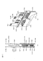
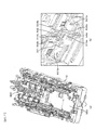
- FIG. 17A is an external perspective view in which a power module, a capacitor module, and a bus bar module are assembled to the cooling jacket 12.
- FIG. 17B is an enlarged view of a solid line encircled portion in FIG.
- the DC positive terminal 315B, the DC negative terminal 319B, the AC terminal 321 and the external signal terminals 325U and 325L pass through the through hole 519 of the capacitor case 502 to the upper side of the flange portion 515a. It extends.
- the area of the current path of the DC positive terminal 315B and the DC negative terminal 319B is much smaller than the area of the current path of the laminated conductor plate 501. Therefore, when the current flows from the laminated conductor plate 501 to the DC positive terminal 315B and the DC negative terminal 319B, the area of the current path changes greatly. That is, the current is concentrated on the DC positive terminal 315B and the DC negative terminal 319B.
- the negative-side capacitor terminal 504a includes a rising portion 540 rising from the laminated conductor plate 501, a folded portion 541 connected to the rising portion 540 and bent in a U shape, and the folded portion 541. And a connection portion 542 whose surface opposite to the rising portion 540 is opposed to the main surface of the DC negative electrode terminal 319B.
- the positive electrode side capacitor terminal 506a has a rising portion 543 rising from the laminated conductor plate 501, a folded portion 544, a surface connected to the folded portion 544 and opposite to the rising portion 543 of the DC positive electrode terminal 315B. And a connecting portion 545 facing the main surface.
- the folded portion 544 is configured to be connected to the rising portion 543 at a substantially right angle and straddle the side portions of the negative capacitor terminal 504a, the DC positive terminal 315B, and the DC negative terminal 319B. Further, the main surface of the rising portion 540 and the main surface of the rising portion 543 are opposed to each other with the insulating sheet 517 interposed therebetween. Similarly, the main surface of the folded portion 541 and the main surface of the folded portion 544 are opposed to each other with the insulating sheet 517 interposed therebetween.
- the capacitor terminal 503a forms a laminated structure through the insulating sheet 517 until just before the connection portion 542, the wiring inductance of the capacitor terminal 503a where current concentrates can be reduced.
- the folded portion 544 is configured to straddle the side portions of the negative electrode side capacitor terminal 504a, the DC positive electrode terminal 315B, and the DC negative electrode terminal 319B. Furthermore, the tip of the DC negative terminal 319B and the side of the connecting portion 542 are connected by welding, and similarly, the tip of the DC positive terminal 315B and the side of the connecting portion 545 are connected by welding.
- the tip of the AC terminal 321 is connected to the tip of the AC bus bar 802a by welding.
- a production facility for welding making the welding machine movable in a plurality of directions with respect to an object to be welded leads to a complicated production facility, which is not preferable from the viewpoint of productivity and cost. Therefore, in the present embodiment, the welding location of the AC terminal 321 and the welding location of the DC negative electrode terminal 319 ⁇ / b> B are arranged in a straight line along the longitudinal side of the cooling jacket 12. Thereby, it is possible to perform a plurality of weldings while moving the welding machine in one direction, and productivity is improved.
- the plurality of power modules 300a to 300c are arranged in a straight line along the side in the longitudinal direction of the cooling jacket 12. As a result, productivity can be further improved when welding the plurality of power modules 300a to 300c.
- FIG. 18 is an exploded perspective view of the cooling jacket 12 and the bus bar module 800 assembled with the power module and the capacitor module.
- FIG. 19 is an external perspective view of the bus bar module 800 with the holding member 803 removed.
- the capacitor case 502 shown in FIG. 16 is disposed between the fuse material 700 provided in the power module 300 and the positive conductor plate 505 and the negative conductor plate 507 provided in the capacitor module 500.
- Flange portions 515 a and 515 b of the capacitor case 502 exist between the positive electrode conductor plate 505 and the negative electrode conductor plate 507 and the fuse material 700.
- the DC positive terminal 315B and the DC negative terminal 319B protrude from the through holes 519 formed in the flange portions 515a and 515b of the capacitor case 502 and extend away from the openings formed in the flow paths.
- the positive conductor plate 505 and the negative conductor plate 507 are protected by the flange portions 515 a and 515 b of the capacitor case 502. For this reason, even if the fuse material 700 is melted, the positive conductor plate 505 and the negative conductor plate 507 are not affected, and the breakdown can be minimized, so that the reliability is improved.
- the first AC bus bars 802a to 802f are stacked conductors of the capacitor module 500 up to the installation location of the current sensor 180a or current sensor 180b. It is formed so as to be substantially perpendicular to the main surface of the plate 501. Further, the first AC bus bars 802a to 802f are bent substantially at right angles immediately before the through hole of the current sensor 180a or the through hole of the current sensor 180b. Thereby, the main surface of the portion of the first AC bus bars 802a to 802f that penetrates the current sensor 180a or the current sensor 180b is substantially parallel to the main surface of the multilayer conductor plate 501. Then, connection portions 805a to 805f for connecting to the second AC bus bars 804a to 804f are formed at the end portions of the first AC bus bars 802a to 802f (connection portions 805d to 805f are not shown).
- the second AC bus bars 804a to 804f are bent at substantially right angles toward the capacitor module 500 side in the vicinity of the connection portions 805a to 805f.
- the main surfaces of the second AC bus bars 804a to 804f are formed so as to be substantially perpendicular to the main surface of the multilayer conductor plate 501 of the capacitor module 500.
- the second AC bus bars 804a to 804f are extended from the vicinity of the current sensor 180a or the current sensor 180b toward one side 12a in the short direction of the cooling jacket 12 shown in FIG. It is formed to cross. That is, the second AC bus bars 804a to 804f are formed so as to cross the side 12a with the main surfaces of the plurality of second AC bus bars 804a to 804f facing each other.
- the first AC bus bars 802a to 802f, the current sensors 180a to 180b, and the second AC bus bars 804a to 804f are held and insulated by a holding member 803 made of resin.
- the second AC bus bars 804a to 804f improve the insulation between the metal cooling jacket 12 and the housing 119. Further, since the holding member 803 is in thermal contact with or directly in contact with the cooling jacket 12, heat transmitted from the transmission 118 side to the second AC bus bars 804a to 804f can be released to the cooling jacket 12, so that the current sensors 180a to The reliability of 180b can be improved.
- the holding member 803 is provided with a support member 807a and a support member 807b for indicating the driver circuit board 22 shown in FIG.
- a plurality of support members 807 a are provided and are arranged in a line along one side in the longitudinal direction of the cooling jacket 12. Further, a plurality of support members 807 b are provided, and are formed in a line along the other side in the longitudinal direction of the cooling jacket 12. Screw holes for fixing the driver circuit board 22 are formed at the distal ends of the support member 807a and the support member 807b.
- the holding member 803 is provided with a protruding portion 806a and a protruding portion 806b that extend upward from locations where the current sensor 180a and the current sensor 180b are disposed.
- the protrusion 806a and the protrusion 806b are configured to penetrate the current sensor 180a and the current sensor 180b, respectively.
- the current sensor 180 a and the current sensor 180 b are provided with a signal line 182 a and a signal line 182 b that extend in the arrangement direction of the driver circuit board 22.
- the signal line 182a and the signal line 182b are joined to the wiring pattern of the driver circuit board 22 by solder.
- the holding member 803, the support members 807a to 807b, and the protrusions 806a to 806b are integrally formed of resin.
- the holding member 803 has a function of positioning the current sensor 180 and the driver circuit board 22, the assembly and solder connection work between the signal line 182a and the driver circuit board 22 is facilitated. Further, by providing the holding member 803 with a mechanism for holding the current sensor 180 and the driver circuit board 22, the number of components as the whole power conversion device can be reduced.
- the holding member 803 is provided with a support member 808 for indicating the vicinity of the center portion of the driver circuit board 22 to reduce the influence of vibration applied to the driver circuit board 22.
- the holding member 803 is fixed to the cooling jacket 12 with screws.
- the holding member 803 is provided with a bracket 809 for fixing one end of the auxiliary power module 350.
- the auxiliary power module 350 is disposed in the protruding portion 407, whereby the other end of the auxiliary power module 350 is fixed to the protruding portion 407. Thereby, the influence of vibration applied to the auxiliary power module 350 can be reduced, and the number of parts for fixing can be reduced.
- FIG. 20 is an external perspective view of the cooling jacket 12 in which the power module, the capacitor module, the bus bar module 800, and the auxiliary power module 350 are assembled.
- the current sensor 180 may be destroyed when heated to a temperature of about 100 ° C. or higher.
- the temperature of the environment in which it is used becomes very high, so it is important to protect the current sensor 180 from heat.
- the power conversion device 200 according to the present embodiment is mounted on the transmission 118, it is important to protect it from heat generated from the transmission 118.
- the current sensor 180a and the current sensor 180b are disposed on the opposite side of the transmission 118 with the cooling jacket 12 interposed therebetween. This makes it difficult for the heat generated by the transmission 118 to be transmitted to the current sensor, and suppresses an increase in the temperature of the current sensor.
- the second AC bus bars 804a to 804f are formed so as to cross the flow direction 810 of the refrigerant flowing through the third flow path 19c shown in FIG.
- the current sensor 180a and the current sensor 180b are arranged closer to the AC terminal 321 of the power module than the portions of the second AC bus bars 804a to 804f crossing the third flow path portion 19c.
- the second AC bus bars 804a to 804f are indirectly cooled by the refrigerant, and heat transmitted from the AC bus bar to the current sensor and further to the semiconductor chip in the power module can be relieved, thereby improving the reliability.
- the flow direction 811 shown in FIG. 20 indicates the flow direction of the refrigerant flowing through the fourth flow path 19d shown in FIG.
- the flow direction 812 indicates the flow direction of the refrigerant flowing through the second flow path 19b shown in FIG.
- the current sensor 180a and the current sensor 180b according to the present embodiment are arranged so that the projection portions of the current sensor 180a and the current sensor 180b are surrounded by the projection portion of the flow path 19 when projected from above the power conversion device 200. The This further protects the current sensor from heat from the transmission 118.
- FIG. 21 is a divided perspective view of the power conversion device 200 in which the control circuit board 20 and the metal base plate 11 are separated.
- the driver circuit board 22 is fixed to support members 807a and 807b formed on the bus bar module 800. Further, the driver board 22 is disposed above the DC positive terminal 315B and the DC negative terminal 319B protruding from the through holes 519 formed in the flange portions 515a and 515b of the capacitor case 502. With this configuration, since the influence of the heat received by the driver circuit board 22 when the fuse material 700 is melted is reduced, the driver circuit board 22 is not easily broken, and the reliability is improved.
- the cooling jacket 12 has a support member 15, and the support member 15 extends so as to be separated from the opening 400 formed in the cooling jacket 12.
- the control circuit board 20 is fixed to the metal base plate 11 held by the support member 15, and the metal base plate 11 is disposed above the DC positive terminal 315B and the DC negative terminal 319B. Since the metal base plate 11 is disposed between the control circuit board 20 and the fuse material 700 as described above, the influence of heat applied to the control circuit board 20 is reduced when the fuse material 700 is melted, so that it is difficult to be destroyed. And reliability is improved.
- the current sensor 180 is disposed above the capacitor module 500.
- the driver circuit board 22 is disposed above the current sensor 180 and supported by support members 807a and 807b provided in the bus bar module 800 shown in FIG.
- the metal base plate 11 is disposed above the driver circuit board 22 and supported by a plurality of support members 15 erected from the cooling jacket 12.
- the control circuit board 20 is disposed above the metal base plate 11 and is fixed to the metal base plate 11.
- the current sensor 180, the driver circuit board 22 and the control circuit board 20 are hierarchically arranged in a row in the height direction, and the control circuit board 20 is arranged at a position farthest from the high-power system power modules 300 and 301, Mixing of switching noise or the like can be suppressed. Furthermore, the metal base plate 11 is electrically connected to a cooling jacket 12 that is electrically connected to the ground. The metal base plate 11 reduces noise mixed from the driver circuit board 22 into the control circuit board 20.
- the cooling target of the refrigerant flowing in the flow path 19 is mainly the driving power modules 300 and 301
- the power modules 300 and 301 are housed in the flow path 19 and directly contact the refrigerant. And cooled.
- the auxiliary power module 350 is also required to be cooled, although not as much as the driving power module.
- the heat radiating surface formed of the metal base of the auxiliary power module 350 is formed so as to face the inlet pipe 13 and the outlet pipe 14 through the flow path 19.
- the protruding portion 407 for fixing the auxiliary power module 350 is formed above the inlet pipe 13, the refrigerant flowing from below collides with the inner wall of the protruding portion 407, and the auxiliary power module efficiently. Heat can be taken from 350.
- a space connected to the flow path 19 is formed inside the protruding portion 407.
- the space inside the protrusion 407 increases the depth of the flow path 19 in the vicinity of the inlet pipe 13 and the outlet pipe 14, and a liquid pool is generated in the space inside the protrusion 407.
- the auxiliary power module 350 can be efficiently cooled by this liquid pool.
- the driver circuit board 22 of the present embodiment is formed with a first hole 24 and a second hole 26 that penetrate the driver circuit board 22. Further, the external signal terminal 325U and the external signal terminal 325L of the power module 300 are inserted into the first hole 24, and the external signal terminal 325U and the external signal terminal 325L are joined to the wiring pattern of the driver circuit board 22 by soldering. Further, the signal line 182 of the current sensor 180 is inserted into the second hole 26, and the signal line 182 is joined to the wiring pattern of the driver circuit board 22 by solder. Note that solder bonding is performed from the surface side of the driver circuit board 22 opposite to the surface facing the cooling jacket 12.
- productivity can be further improved by joining the external signal terminal 325 of the power module 300 and the signal line 182 of the current sensor 180 by solder from the same direction. Further, by providing the driver circuit board 22 with the first hole 24 for penetrating the external signal terminal 325 and the second hole 26 for penetrating the signal line 182, the risk of connection mistakes can be reduced. it can.
- the driver circuit board 22 of the present embodiment has a drive circuit (not shown) such as a driver IC chip mounted on the surface facing the cooling jacket 12.
- a drive circuit such as a driver IC chip mounted on the surface facing the cooling jacket 12.
- the heat of solder bonding is suppressed from being transmitted to the driver IC chip or the like, and damage to the driver IC chip or the like due to solder bonding is prevented.
- a high-profile component such as a transformer mounted on the driver circuit board 22 is disposed in the space between the capacitor module 500 and the driver circuit board 22, the entire power conversion device 200 can be reduced in height. Is possible.
- FIG. 22 is a cross-sectional view of the power conversion device 200 cut along the plane B of FIG. 21 as viewed from the C direction.
- the flange 304B provided in the module case 304 is pressed against the cooling jacket 12 by the flange 515a or the flange 515b provided in the capacitor case 502. That is, the airtightness of the flow path 19 can be improved by pressing the module case 304 against the cooling jacket 12 using the dead weight of the capacitor case 502 in which the capacitor cell 514 is accommodated.
- the refrigerant in the flow path 19 it is necessary to allow the refrigerant in the flow path 19 to flow through the region where the fins 305 are formed.
- the fin 305 is not formed in the lower part of the module case 304 in order to secure the space of the curved portion 304A. Therefore, the lower cover 420 is formed so that the lower part of the module case 304 is fitted into the recess 430 formed in the lower cover 420. Thereby, it can prevent that a refrigerant
- the arrangement direction of the power module 300, the capacitor module 500, and the power module 301 is arranged side by side so as to cross the arrangement direction of the control circuit board 20, the driver circuit board 22, and the transmission 118.
- the power module 300, the capacitor module 500, and the power module 301 are arranged side by side in the lowest layer in the power conversion device 200. As a result, the power converter 200 as a whole can be reduced in height, and the influence of vibration from the transmission 118 can be reduced.
- the second embodiment will be described.
- the shape of the auxiliary mold body 600 is changed.
- the other points are the same as in the first embodiment.
- FIG. 23A is a perspective view of the auxiliary mold body 660 used in the second embodiment, and FIG. 23B is a transparent view of the auxiliary mold body 600.
- FIG. 23B is a transparent view of the auxiliary mold body 600.
- the main difference from the first embodiment is that the DC positive terminal 315B, the DC negative terminal 319B, and the AC terminal 321 are arranged between the external signal terminal 325U and the external signal terminal 325L and are held by the auxiliary mold body 660. It is. With this arrangement, the space for welding the DC positive terminal 315B, the DC negative terminal 319B, and the AC terminal 321 can be made larger than when the auxiliary mold body 600 of the first embodiment is used. Further, by taking a large space for welding, the signal conductor 324 is hardly affected by heat during welding, and the signal conductor 324 can be prevented from being destroyed during welding. These configurations improve productivity and reliability.
- Sealing portion 601A has a shape extending in a direction crossing the major axis of the shape of DC positive electrode wiring 315A, DC negative electrode wiring 319A or AC wiring 320 shown in FIG.
- the second sealing portion 601B has a shape extending in a direction substantially parallel to the major axis of the shape of the DC positive electrode wiring 315A, the DC negative electrode wiring 319A, or the AC wiring 320.
- the second sealing portion 601B includes a sealing portion for sealing the external signal terminal 325U on the upper arm side and a sealing portion for sealing the external signal terminal 325L on the lower arm side. The Since the signal wiring 324 is covered with the second sealing portion 601B, the signal wiring 324 is not destroyed even when the fuse material 700 is melted, so that the reliability is improved.
- the sealing portion 601A has a hollow shape, and a wiring fitting portion 602B for fitting the DC negative electrode wiring 319A is formed in the hollow.
- the sealing part 601A has a hollow shape and forms a wiring fitting part 602A for fitting the DC positive electrode wiring 315A into the hollow.
- the sealing portion 601A is disposed on the side of the wiring fitting portion 602A, has a hollow shape, and further forms a wiring fitting portion 602C for fitting the AC wiring 320 into the hollow.
- Each wiring is positioned by fitting each wiring to these wiring fitting portions 602A to 602C. Thereby, it becomes possible to perform the filling operation of the resin sealing material after firmly fixing each wiring, and the mass productivity is improved.
- the wiring insulating part 608 protrudes in a direction away from the sealing part 601A from between the wiring fitting part 602A and the wiring fitting part 602B. Since the plate-shaped wiring insulating portion 608 is interposed between the DC positive electrode wiring 315A and the DC negative electrode wiring 319A, it is possible to arrange the wiring insulating portion 608 so as to reduce the inductance while ensuring insulation.
- the auxiliary mold body 600 supporting each wiring is inserted into a mold preheated to about 150 to 180 ° C.
- the auxiliary mold body 600, the DC positive electrode wiring 315A, the DC negative electrode wiring 319A, the AC wiring 320, the conductor plate 315, the conductor plate 316, the conductor plate 318, and the conductor plate 319 are firmly connected to each other.
- the second sealing portion 601B is formed to extend from the vicinity of the module case 304 to the vicinity of the driver circuit board 22.
- the switching control signal can be normally transmitted even when exposed to a high electric field.
- the DC positive electrode wiring 315A, the DC negative electrode wiring 319A, the AC wiring 320, the external signal terminal 325U and the external signal terminal 325L protrude from the module case 304 in the same direction, electrical insulation can be ensured, and reliability is ensured. Can be secured.
- the difference from the first embodiment is that in the first embodiment, the DC negative electrode wiring 319A, the DC negative terminal 319B, and the fuse material 700 are assembled in a shape that is not a single plate. 319A, DC negative terminal 319B, and fuse material 700 in the form of a single plate are used as a new insert bus bar 711.
- the other configuration is the same as that of the first embodiment.
- FIG. 24A is a diagram excluding the module case 304 and the first sealing resin material 348 of the power module 300
- FIG. 24B is a diagram in which the power module of FIG. is there.
- the fuse material 710 is bonded by being caulked to the DC negative terminal 319B and the DC negative wiring 319A.
- the fuse material 700 is disposed away from the DC positive electrode wiring 315A, the inductance is slightly increased as compared with the case where the DC positive electrode wiring and the DC negative electrode wiring are arranged to face each other. There was a problem that.
- the fuse material 710, the insert bus bar 711, and the DC negative electrode wiring 712 are formed as a single plate as the negative electrode conductor plate, the negative electrode side wiring can be opposed without being away from the DC positive electrode wiring 315A. With such a configuration, the inductance of the entire circuit is reduced, and the temperature rise to the extent that the fuse material is melted can be prevented in advance, thereby improving the reliability.
- the auxiliary mold body 600 since the negative electrode conductor plate insert-molded in the auxiliary mold body 600 has the recessed portion 620 in which the peripheral portion of the fuse material 710 is recessed, the auxiliary mold body 600 is not in direct contact with the auxiliary mold body 600 that easily generates heat. The mold body does not increase excessively. With such a configuration, it is possible to prevent the fuse material from being melted except when abnormal heat is generated, so that reliability is improved.
- the auxiliary mold body 600 of the first embodiment has been described.
- the auxiliary mold body 600 used in the second embodiment may be used.
- the fourth embodiment will be described.
- the difference from the first embodiment is that in the first embodiment, the thickness of the DC negative electrode wiring 319A is substantially constant, and the thickness of the DC negative electrode terminal 319B is also substantially constant, but in the fourth embodiment, it is exposed.
- the thickness of the parts 1701 and 1702 is made thinner than the thickness of the DC negative electrode terminal 319B and the DC negative electrode wiring 319A, and the fuse material 700 is assembled to the portions.
- the figure is shown in FIG. With such a configuration, the fuse material 700 is closer to the DC positive electrode wiring 315A than in the first embodiment, and the increase in inductance can be further suppressed. Therefore, the fuse material 700 generates heat due to generation of a surge voltage, and the fuse material due to the heat generation. Since the fusing of 700 itself can be prevented, the reliability is improved.
- an exposed portion 2702 connected to the DC negative electrode wiring 319A and an exposed portion 2701 connected to the DC negative electrode terminal 319B are bent and formed.
- the figure is shown in FIG.
- the fuse material 700 can be brought close to the DC positive electrode wiring 315A and bonded.
- an increase in inductance can be suppressed more than in the first embodiment, so that the fuse material 700 generates heat due to generation of a surge voltage and the fusing of the fuse material 700 itself due to the heat generation can be prevented.
- the auxiliary mold body 600 of the first embodiment has been described.
- the auxiliary mold body 600 used in the second embodiment may be used.
- a highly reliable semiconductor device, power module, and power conversion device including the power module can be provided.
Landscapes
- Engineering & Computer Science (AREA)
- Microelectronics & Electronic Packaging (AREA)
- Physics & Mathematics (AREA)
- Thermal Sciences (AREA)
- Inverter Devices (AREA)
- Cooling Or The Like Of Semiconductors Or Solid State Devices (AREA)
Abstract
パワーモジュールは、半導体チップと、一方の主面が半導体チップの一方の主面と接続される第1の接続導体と、一方の主面が半導体チップの他方の主面と接続される第2の接続導体と、直流電源から電力が供給される接続端子と、半導体チップを封止する樹脂材とを有し、樹脂材は、第1及び第2の接続導体が対向して形成された空間から突出した突出部を有し、接続端子は突出部に固定され、第1又は第2の接続導体の少なくとも一方は、所定の温度で溶断する金属材を介して接続端子に接続される。
Description
本発明は、半導体素子を内蔵するパワーモジュール、およびパワーモジュールを備えた電力変換装置に関する。
近年電力変換装置では、大電流を流すことができるものが求められている一方、小型化も要求されている。上記電力変換装置で大電流を流そうとすると、半導体素子からの発熱が大きくなり、上記電力変換装置の熱容量を大きくしなければ半導体素子の耐熱温度に達してしまい、小型化の妨げとなる。そこで上記半導体素子を両面から冷却することにより冷却効率を向上させる両面冷却型のパワーモジュールが開発されている。
上記両面冷却型のパワーモジュールは半導体素子の両主面を板状導体であるリードフレームで挟み込み、半導体素子の主面と対向する面と反対側のリードフレームの面が冷却媒体と熱的に接続され、冷却される。
特許文献1にはパワー素子の一方の主面及び他方の主面にパワーリードが突出したヒートシンクが接続され、上記パワー素子及び上記ヒートシンクをモールド樹脂で封止し、そのモールド樹脂の外部に突出したパワーリードと端子部の間にヒューズ部材を設けるという発明が開示されている。
しかし、1つのインバータに複数のパワーモジュールが搭載され、そのパワーモジュール1つ1つにヒューズを設ける場合には更なる信頼性の向上が求められる。
本発明の第1の態様によると、半導体チップと、一方の主面が半導体チップの一方の主面と接続される第1の接続導体と、一方の主面が半導体チップの他方の主面と接続される第2の接続導体と、直流電源から電力が供給される接続端子と、半導体チップを封止する樹脂材とを有し、樹脂材は、第1及び第2の接続導体が対向して形成された空間から突出した突出部を有し、接続端子は突出部に固定され、第1又は第2の接続導体の少なくとも一方は、所定の温度で溶断する金属材を介して接続端子に接続されるパワーモジュール。
本発明の第2の態様によると、第1の態様のパワーモジュールであって、開口部を備える有底の構造で、かつ第1の冷却面および当該第1の冷却面と対向する第2の冷却面を有する冷却器を備え、第1の接続導体における他方の主面は第1の冷却面と対向して配置され、第2の接続導体における他方の主面は第2の冷却面と対向して配置され、突出部は開口部から冷却器の外部に突出しており、金属材は開口部から突出した突出部に配置されるのが好ましい。
本発明の第3の態様によると、第2の態様のパワーモジュールであって、第1の接続導体における他方の主面と、第1の冷却面との間に配置されている第1の絶縁部材と、第2の接続導体における他方の主面と、第2の冷却面との間に配置されている第2の絶縁部材を有するのが好ましい。
本発明の第4の態様によると、第2乃至3の態様のいずれかのパワーモジュールであって、半導体チップはIGBTから構成され、かつ、IGBTの一方の主面はコレクタ電極を形成し、IGBTの他方の主面はエミッタ電極を形成し、接続端子は、第1の接続導体を介してIGBTのコレクタ電極に電気的に接続される正極接続端子と、第2の接続導体を介してIGBTのエミッタ電極に電気的に接続される負極接続端子と、を含んで構成され、第2の接続導体は、金属材を介して負極接続端子と接続されるのが好ましい。
本発明の第5の態様によると、半導体チップと、半導体チップの主面に接続される板状導体と、直流電源に電気的に接続される接続端子と、板状導体を封止する樹脂材を有するパワーモジュールと、冷却媒体が流れる流路を有する流路形成体と、を有し、流路形成体は、所定の面に流路と接続される開口を有し、パワーモジュールは開口から流路内に浸漬され、樹脂材は、開口から突出する突出部を有し、接続端子は突出部に固定され、板状導体の一部は所定の温度で溶断する金属材を介して接続端子と接続される電力変換装置。
本発明の第6の態様によると、第5の態様の電力変換装置であって、第1の冷却面と当該第1の冷却面と対向する第2の冷却面を有し、かつ、開口部を有する有底の冷却器を備え、 冷却器はパワーモジュールを収納し、板状導体は、半導体チップの一方の主面と対向して配置される第1の板状導体と、半導体チップの他方の主面と対向して配置される第2の板状導体から構成され、かつ、当該第1の板状導体は第1の絶縁部材を介して第1の冷却面と対向して配置され、当該第2の板状導体は第2の絶縁部材を介して第2の冷却面と対向して配置されるのが好ましい。
本発明の第7の態様によると、第6の態様の電力変換装置であって、冷却器は、開口部が形成された当該冷却器の一面にフランジ部を有し、フランジ部の開口部が形成された面とは反対側の当該フランジ部の面が流路形成体に固定されるのが好ましい。
本発明の第8の態様によると、第6乃至7の態様のいずれかの電力変換装置であって、コンデンサセルと、当該コンデンサセルを収納するコンデンサケースを有するコンデンサモジュールを備え、コンデンサケースは孔が形成されたフランジ部を有し、パワーモジュールの接続端子はコンデンサケースの孔を貫通し、金属材は冷却器のフランジ部とコンデンサケースのフランジ部が対向して形成された空間に配置されているのが好ましい。
本発明の第9の態様によると、第5乃至8の態様のいずれかの電力変換装置であって、半導体チップを駆動するドライバ回路基板を備え、接続端子は、当該接続端子の端部が流路形成体の開口から遠ざかる方向に延び、ドライバ回路基板の主面が開口と対向し、かつ、当該ドライバ回路基板は接続端子の端部より上方に配置されるのが好ましい。
本発明の第10の態様によると、第5乃至8の態様のいずれかの電力変換装置であって、半導体チップを制御するための制御信号を生成する制御回路基板と、制御回路基板を保持する金属ベースを有し、金属ベースは、流路形成体と制御回路基板の間に配置されるのが好ましい。
本発明により、パワーモジュール、およびパワーモジュールを備えた電力変換装置の信頼性が向上する。
本実施形態に係る電力変換装置200は、ハイブリッド用の自動車や純粋な電気自動車に適用可能であるが、代表例として、ハイブリッド自動車に適用した場合における制御構成と回路構成について、図1と図2を用いて説明する。
図1は、ハイブリッド自動車の制御ブロックを示す図である。
本実施形態に係る電力変換装置では、車両駆動用電機システムに用いられ、搭載環境や動作的環境などが大変厳しい車両駆動用インバータ装置を例に挙げて説明する。なお、本実施形態の構成は、自動車やトラックなどの車両駆動用電力変換装置として最適であるが、これら以外の電力変換装置、例えば電車や船舶,航空機などの電力変換装置、さらに工場の設備を駆動する電動機の制御装置として用いられる産業用電力変換装置、或いは家庭の太陽光発電システムや家庭の電化製品を駆動する電動機の制御装置に用いられたりする家庭用電力変換装置に対しても適用可能である。
図1において、ハイブリッド電気自動車(以下、「HEV」と記述する)110は1つの電動車両であり、2つの車両駆動用システムを備えている。その1つは、内燃機関であるエンジン120を動力源としたエンジンシステムである。エンジンシステムは、主としてHEVの駆動源として用いられる。もう1つは、モータジェネレータ192,194を動力源とした車載電機システムである。車載電機システムは、主としてHEVの駆動源及びHEVの電力発生源として用いられる。モータジェネレータ192,194は例えば同期機あるいは誘導機であり、運転方法によりモータとしても発電機としても動作するので、ここではモータジェネレータと記す。
車体のフロント部には前輪車軸114が回転可能に軸支され、前輪車軸114の両端には1対の前輪112が設けられている。車体のリア部には後輪車軸が回転可能に軸支され、後輪車軸の両端には1対の後輪が設けられている(図示省略)。本実施形態のHEVでは、いわゆる前輪駆動方式を採用しているが、この逆、すなわち後輪駆動方式を採用しても構わない。前輪車軸114の中央部には前輪側デファレンシャルギア(以下、「前輪側DEF」と記述する)116が設けられている。前輪側DEF116の入力側にはトランスミッション118の出力軸が機械的に接続されている。トランスミッション118の入力側にはモータジェネレータ192の出力側が機械的に接続されている。モータジェネレータ192の入力側には動力分配機構122を介してエンジン120の出力側及びモータジェネレータ194の出力側が機械的に接続されている。
インバータ部140,142は、直流コネクタ138を介してバッテリ136と電気的に接続される。バッテリ136とインバータ部140,142との相互において電力の授受が可能である。本実施形態では、モータジェネレータ192及びインバータ部140からなる第1電動発電ユニットと、モータジェネレータ194及びインバータ部142からなる第2電動発電ユニットとの2つを備え、運転状態に応じてそれらを使い分けている。なお、本実施形態では、バッテリ136の電力によって第1電動発電ユニットを電動ユニットとして作動させることにより、モータジェネレータ192の動力のみによって車両の駆動ができる。さらに、本実施形態では、第1電動発電ユニット又は第2電動発電ユニットを発電ユニットとしてエンジン120の動力或いは車輪からの動力によって作動させて発電させることにより、バッテリ136の充電ができる。
バッテリ136はさらに補機用のモータ195を駆動するための電源としても使用される。補機としては例えば、エアコンディショナーのコンプレッサを駆動するモータ、あるいは制御用の油圧ポンプを駆動するモータである。バッテリ136からインバータ部43に直流電力が供給され、インバータ部43で交流の電力に変換されてモータ195に供給される。インバータ部43は、インバータ部140や142と同様の機能を持ち、モータ195に供給する交流の位相や周波数,電力を制御する。モータ195の容量がモータジェネレータ192や194の容量より小さいので、インバータ部43の最大変換電力がインバータ部140や142より小さいが、インバータ部43の回路構成は基本的にインバータ部140や142の回路構成と同じである。なお、電力変換装置200は、インバータ部140,インバータ部142,インバータ部43に供給される直流電流を平滑化するためのコンデンサモジュール500を備えている。
次に、図2を用いてインバータ部140やインバータ部142あるいはインバータ部43の電気回路構成を説明する。なお、図2では、代表例としてインバータ部140の説明を行う。
インバータ回路144は、上下アーム直列回路150をモータジェネレータ192の電機子巻線の各相巻線に対応して3相(U相,V相,W相)分を設けている。上下アーム直列回路150は、上アームとして動作するIGBT328(絶縁ゲート型バイポーラトランジスタ)及びダイオード156と、下アームとして動作するIGBT330及びダイオード166と、からなる。それぞれの上下アーム直列回路150は、その中点部分(中間電極169)から交流端子159及び交流コネクタ188を通してモータジェネレータ192への交流電力線(交流バスバー)186と接続する。
上アームのIGBT328のコレクタ電極153は正極端子(P端子)157を介してコンデンサモジュール500の正極側のコンデンサの電極に、下アームのIGBT330のエミッタ電極は負極端子(N端子)158を介してコンデンサモジュール500の負極側のコンデンサ電極にそれぞれ電気的に接続されている。
制御部170は、インバータ回路144を駆動制御するドライバ回路174と、ドライバ回路174へ信号線176を介して制御信号を供給する制御回路172と、を有している。IGBT328やIGBT330は、制御部170から出力された駆動信号を受けて動作し、バッテリ136から供給された直流電力を三相交流電力に変換する。この変換された電力は、モータジェネレータ192の電機子巻線に供給される。
IGBT328は、コレクタ電極153と、信号用エミッタ電極155と、ゲート電極154を備えている。また、IGBT330は、コレクタ電極163と、信号用のエミッタ電極165と、ゲート電極164とを備えている。ダイオード156が、コレクタ電極153とエミッタ電極との間に電気的に接続されている。また、ダイオード166が、コレクタ電極163とエミッタ電極との間に電気的に接続されている。スイッチング用パワー半導体素子としてはMOSFET(金属酸化物半導体型電界効果トランジスタ)を用いてもよいが、この場合はダイオード156やダイオード166は不要となる。コンデンサモジュール500は、正極側コンデンサ端子506と負極側コンデンサ端子504と直流コネクタ138とを介してバッテリ136に電気的に接続されている。なお、インバータ部140は、直流正極端子314を介して正極側コンデンサ端子506と接続され、かつ直流負極端子316を介して負極側コンデンサ端子504と接続される。
制御回路172は、IGBT328及びIGBT330のスイッチングタイミングを演算処理するためのマイクロコンピュータ(以下、「マイコン」と記述する)を備えている。マイコンには入力情報として、モータジェネレータ192に対して要求される目標トルク値、上下アーム直列回路150からモータジェネレータ192の電機子巻線に供給される電流値、及びモータジェネレータ192の回転子の磁極位置が入力されている。目標トルク値は、不図示の上位の制御装置から出力された指令信号に基づくものである。電流値は、電流センサ180から信号線182を介して出力された検出信号に基づいて検出されたものである。磁極位置は、モータジェネレータ192に設けられた回転磁極センサ(不図示)から出力された検出信号に基づいて検出されたものである。本実施形態では3相の電流値を検出する場合を例に挙げて説明するが、2相分の電流値を検出するようにしても構わない。
制御回路172内のマイコンは、目標トルク値に基づいてモータジェネレータ192のd,q軸の電流指令値を演算し、この演算されたd,q軸の電流指令値と、検出されたd,q軸の電流値との差分に基づいてd,q軸の電圧指令値を演算し、この演算されたd,q軸の電圧指令値を、検出された磁極位置に基づいてU相,V相,W相の電圧指令値に変換する。そして、マイコンは、U相,V相,W相の電圧指令値に基づく基本波(正弦波)と搬送波(三角波)との比較に基づいてパルス状の変調波を生成し、この生成された変調波をPWM(パルス幅変調)信号として、信号線176を介してドライバ回路174に出力する。
ドライバ回路174は、下アームを駆動する場合、PWM信号を増幅したドライブ信号を、対応する下アームのIGBT330のゲート電極に出力する。また、ドライバ回路174は、上アームを駆動する場合、PWM信号の基準電位のレベルを上アームの基準電位のレベルにシフトしてからPWM信号を増幅し、これをドライブ信号として、対応する上アームのIGBT328のゲート電極にそれぞれ出力する。
また、制御部170は、異常検知(過電流,過電圧,過温度など)を行い、上下アーム直列回路150を保護している。このため、制御部170にはセンシング情報が入力されている。例えば各アームの信号用エミッタ電極155及び信号用エミッタ電極165からは各IGBT328とIGBT330のエミッタ電極に流れる電流の情報が、対応する駆動部(IC)に入力されている。これにより、各駆動部(IC)は過電流検知を行い、過電流が検知された場合には対応するIGBT328,IGBT330のスイッチング動作を停止させ、対応するIGBT328,IGBT330を過電流から保護する。上下アーム直列回路150に設けられた温度センサ(不図示)からは上下アーム直列回路150の温度の情報がマイコンに入力されている。また、マイコンには上下アーム直列回路150の直流正極側の電圧の情報が入力されている。マイコンは、それらの情報に基づいて過温度検知及び過電圧検知を行い、過温度或いは過電圧が検知された場合には全てのIGBT328,IGBT330のスイッチング動作を停止させる。
図3は、本実施形態に係る電力変換装置200の設置場所を説明するための分解斜視図を示す。
本実施形態に係る電力変換装置200は、トランスミッション118を収納するためのアルミニウム製の筐体119に固定される。電力変換装置200は、底面及び上面の形状を略長方形としたことで、車両への取り付けが容易となり、また生産し易い効果がある。冷却ジャケット12は、後述するパワーモジュール300及びコンデンサモジュール500を保持するとともに、冷却媒体によって冷却する。また、冷却ジャケット12は、筐体119に固定され、かつ筐体119との対向面に入口配管13と出口配管14が形成されている。入口配管13と出口配管14が筐体119に形成された配管と接続されることにより、トランスミッション118を冷却するための冷却媒体が、冷却ジャケット12に流入及び流出する。
ケース10は、電力変換装置200を覆って、かつ筐体119側に固定される。ケース10の底は、制御回路172を実装した制御回路基板20と対向するように構成される。またケース10には、ケース10の底から外部に繋がる第1開口202と第2開口204とが、ケース10の底面に形成されている。コネクタ21は、制御回路基板20に接続されており、外部からの各種信号を当該制御回路基板20に伝送する。バッテリ負極側接続端子部510とバッテリ正極側接続端子部512とは、バッテリ136とコンデンサモジュール500とを電気的に接続する。
コネクタ21とバッテリ負極側接続端子部510とバッテリ正極側接続端子部512とは、ケース10の底面に向かって延ばされ、コネクタ21は第1開口202から突出し、かつバッテリ負極側接続端子部510及びバッテリ正極側接続端子部512は第2開口204から突出する。ケース10には、その内壁の第1開口202及び第2開口204の周りにシール部材(不図示)が設けられる。
コネクタ21等の端子の勘合面の向きは、車種により種々の方向となるが、特に小型車両に搭載しようとした場合、エンジンルーム内の大きさの制約や組立性の観点から勘合面を上向きにして出すことが好ましい。特に、本実施形態のように、電力変換装置200が、トランスミッション118の上方に配置される場合には、トランスミッション118の配置側とは反対側に向かって突出させることにより、作業性が向上する。また、コネクタ21は外部の雰囲気からシールする必要がある。本実施の形態では、コネクタ21に対してケース10を上方向から組付ける構成となることで、ケース10が筐体119に組付けられたときに、ケース10と接触するシール部材がコネクタ21を押し付けることができ、気密性が向上する。
図4は、本実施形態に係る電力変換装置の全体構成を各構成要素に分解した斜視図である。
冷却ジャケット12には、流路19(図5)が設けられ、該流路19の上面には、開口部400a~400cが冷媒の流れ方向418に沿って形成され、かつ開口部402a~402cが冷媒の流れ方向422に沿って形成される。開口部400a~400cがパワーモジュール300a~300cによって塞がれる様に、かつ開口部402a~402cがパワーモジュール301a~301cによって塞がれる。
また、冷却ジャケット12には、コンデンサモジュール500を収納するための収納空間405が形成される。コンデンサモジュール500は、収納空間405に収納されることにより、流路19内に流れる冷媒によって冷やされることになる。コンデンサモジュール500は、冷媒の流れ方向418を形成するための流路19と、冷媒の流れ方向422を形成するための流路19とに挟まれるため、効率良く冷却することができる。
冷却ジャケット12には、入口配管13と出口配管14と対向する位置に突出部407が形成される。突出部407は、冷却ジャケット12と一体に形成される。補機用パワーモジュール350は、突出部407に固定され、流路19内に流れる冷媒によって冷やされることになる。補機用パワーモジュール350の側部には、バスバーモジュール800が配置される。バスバーモジュール800は、交流バスバー186や電流センサ180等により構成されるが、詳細は後述する。
このように冷却ジャケット12の中央部にコンデンサモジュール500の収納空間405を設け、その収納空間405を挟むように流路19を設け、それぞれの流路19に車両駆動用のパワーモジュール300a~300c及びパワーモジュール301a~301cを配置し、さらに冷却ジャケット12の上面に補機用パワーモジュール350を配置する。このため、少ない空間で効率良く冷却でき、電力変換装置全体の小型化が可能となる。また冷却ジャケット12の流路19の主構造を冷却ジャケット12と一体にアルミ材の鋳造で作ることにより、流路19は冷却効果に加え機械的強度を強くする効果がある。またアルミ鋳造で作ることで冷却ジャケット12と流路19とが一体構造となり、熱伝導が良くなり冷却効率が向上する。
なお、パワーモジュール300a~300cとパワーモジュール301a~301cを流路19に固定することで流路19を完成させ、水路の水漏れ試験を行う。水漏れ試験に合格した場合に、次にコンデンサモジュール500や補機用パワーモジュール350や基板を取り付ける作業を行うことができる。このように、電力変換装置200の底部に冷却ジャケット12を配置し、次にコンデンサモジュール500,補機用パワーモジュール350,バスバーモジュール800,基板等の必要な部品を固定する作業を上から順次行えるように構成されており、生産性と信頼性が向上する。
ドライバ回路基板22は、補機用パワーモジュール350及びバスバーモジュール800の上方に配置される。また、ドライバ回路基板22と制御回路基板20の間には金属ベース板11が配置される。金属ベース板11は、ドライバ回路基板22及び制御回路基板20に搭載される回路群の電磁シールドの機能を奏すると共にドライバ回路基板22と制御回路基板20とが発生する熱を逃がし、冷却する作用を有している。
図5は、流路19を有する冷却ジャケット12の下面図である。
冷却ジャケット12と当該冷却ジャケット12の内部に設けられた流路19とは、一体に鋳造されている。冷却ジャケット12に下面には、1つに繋がった開口部404が形成されている。開口部404は、中央部に開口を有する下カバー420によって塞がれる。下カバー420と冷却ジャケット12との間には、シール部材409a及びシール部材409bが設けられ気密性を保っている。
下カバー420には、一方の端辺の近傍であって当該端辺に沿って、入口配管13を挿入するための入口孔401と、出口配管14を挿入するための出口孔403が形成される。また下カバー420には、トランスミッション118の配置方向に向かって突出する凸部406が形成される。凸部406は、パワーモジュール300a~300c及びパワーモジュール301a~301c毎に設けられる。
冷媒は、流れ方向417のように、入口孔401を通って、冷却ジャケット12の短手方向の辺に沿って形成された第1流路部19aに向かって流れる。そして冷媒は、流れ方向418のように、冷却ジャケット12の長手方向の辺に沿って形成された第2流路部19bを流れる。また冷媒は、流れ方向421のように、冷却ジャケット12の短手方向の辺に沿って形成された第3流路部19cを流れる。第3流路部19cは折り返し流路を形成する。また、冷媒は、流れ方向422のように、冷却ジャケット12の長手方向の辺に沿って形成された第4流路部19dを流れる。第4流路部19dは、コンデンサモジュール500を挟んで第2流路部19bと対向する位置に設けられる。さらに、冷媒は、流れ方向423のように、冷却ジャケット12の短手方向の辺に沿って形成された第5流路部19e及び出口孔403を通って出口配管14に流出する。
第1流路部19a,第2流路部19b,第3流路部19c,第4流路部19d及び第5流路部19eは、いずれも幅方向より深さ方向が大きく形成される。パワーモジュール300a~300cが、冷却ジャケット12の上面側に形成された開口部400a~400cから挿入され(図4参照)、第2流路部19b内の収納空間に収納される。なお、パワーモジュール300aの収納空間とパワーモジュール300bの収納空間との間には、冷媒の流れを澱ませないための中間部材408aが形成される。同様に、パワーモジュール300bの収納空間とパワーモジュール300cの収納空間との間には、冷媒の流れを澱ませないための中間部材408bが形成される。中間部材408a及び中間部材408bは、その主面が冷媒の流れ方向に沿うように形成される。第4流路部19dも第2流路部19bと同様にパワーモジュール301a~301cの収納空間及び中間部材を形成する。また、冷却ジャケット12は、開口部404と開口部400a~400c及び402a~402cとが対向するように形成されているので、アルミ鋳造により製造し易い構成になっている。
下カバー420には、筐体119と当接し、電力変換装置200を支持するための支持部410a及び支持部410bが設けられる。支持部410aは下カバー420の一方の端辺に近づけて設けられ、支持部410bは下カバー420の他方の端辺に近づけて設けられる。これにより、電力変換装置200を、トランスミッション118やモータジェネレータ192の円柱形状に合わせて形成された筐体119の側壁に強固に固定することができる。
また、支持部410bは、抵抗器450を支持するように構成されている。この抵抗器450は、乗員保護やメンテナンス時における安全面に配慮して、コンデンサセルに帯電した電荷を放電するためのものである。抵抗器450は、高電圧の電気を継続的に放電できるように構成されているが、万が一抵抗器もしくは放電機構に何らかの異常があった場合でも、車両に対するダメージを最小限にするように配慮した構成とする必要がある。つまり、抵抗器450がパワーモジュールやコンデンサモジュールやドライバ回路基板等の周辺に配置されている場合、万が一抵抗器450が発熱,発火等の不具合を発生した場合に主要部品近傍で延焼する可能性が考えられる。
そこで本実施形態では、パワーモジュール300a~300cやパワーモジュール301a~301cやコンデンサモジュール500は、冷却ジャケット12を挟んで、トランスミッション118を収納した筐体119とは反対側に配置され、かつ抵抗器450は、冷却ジャケット12と筐体119との間の空間に配置される。これにより、抵抗器450が金属で形成された冷却ジャケット12及び筐体119で囲まれた閉空間に配置されることになる。なお、コンデンサモジュール500内のコンデンサセルに貯まった電荷は、図4に示されたドライバ回路基板22に搭載されたスイッチング手段のスイッチング動作によって、冷却ジャケット12の側部を通る配線を介して抵抗器450に放電制御される。本実施形態では、スイッチング手段によって高速に放電するように制御される。放電を制御するドライバ回路基板22と抵抗器450との間に、冷却ジャケット12が設けられているので、ドライバ回路基板22を抵抗器450から保護することができる。また、抵抗器450は下カバー420に固定されることにより、流路19と熱的に非常に近い位置に設けられているので、抵抗器450の異常な発熱を抑制することができる。
図6乃至図15を用いてインバータ部140およびインバータ部142に使用されるパワーモジュール300aの詳細構成を説明する。図6(a)は、本実施形態のパワーモジュール300aの斜視図である。図6(b)は、本実施形態のパワーモジュール300aの断面図である。
上下アーム直列回路を構成するパワー半導体素子(IGBT328,IGBT330,ダイオード156,ダイオード166)が、図7乃至図9に示す如く、導体板315や導体板318によって、あるいは導体板316や導体板319によって、両面から挟んで固着される。これら導体板には、外部信号端子325Uや外部信号端子325Lである信号配線を一体成型して成る補助モールド体600が組みつけられる。導体板315等は、その放熱面が露出した状態で第一封止樹脂348によって封止され、当該放熱面に絶縁シート333が熱圧着される。第一封止樹脂348により封止されたモジュール一次封止体302は、モジュールケース304の中に挿入して絶縁シート333を挟んで、CAN型冷却器であるモジュールケース304の内面に熱圧着される。ここで、CAN型冷却器とは、一面に挿入口306と他面に底を有する筒形状をした冷却器である。
モジュールケース304は、アルミ合金材料例えばAl,AlSi,AlSiC,Al-C等から構成され、かつ、つなぎ目の無い状態で一体に成形される。ここでモジュールケース304に使われている材料は具体的にアルミ合金材料を挙げているが、銅や銅合金材料などを用いることも考えられる。銅材料を用いた場合はアルミ合金材料を用いた場合に比べて安価にモジュールケース304を作成することができる。モジュールケース304は、挿入口306以外に開口を設けない構造であり、挿入口306は、フランジ304Bよって、その外周を囲まれている。また、図6(a)に示されるように、他の面より広い面を有する第1放熱面307A及び第2放熱面307Bがそれぞれ対向した状態で配置され、当該対向する第1放熱面307Aと第2放熱面307Bとを繋ぐ3つの面は、当該第1放熱面307A及び第2放熱面307Bより狭い幅で密閉された面を構成し、残りの一辺の面に挿入口306が形成される。この挿入口306から突出している補助モールド体600の近傍にヒューズ材700が配置されている。ヒューズ材700を設けることによって、過電流によるパワーモジュールの破壊を防ぐことができる。また、モジュールケース304は、挿入口400a,400b,400cより直接水路の中に挿入され、モジュールケース304の外表面は冷却媒体と直接接触する。ヒューズ材700をモジュールケース304の内部に配置すると、ヒューズ材700が溶断するときにモジュールケース304が破壊され、さらには漏水による装置全体の破壊を引き起こす可能性がある。そこで本実施例のようにヒューズ材700を挿入口306から突出している補助モールド体600にヒューズ材を設ける。これによって、たとえヒューズ材700が溶断した際であっても、モジュールケース304の破壊を防ぐことができ、信頼性が向上する。また、ヒューズ材700は冷媒が直接接しているモジュールケースの近傍に設けられ、さらに直流負極配線319A及び直流負極端子319Bと接続されている。直流負極配線319Aの一方の面はIGBT328,330及びダイオード156,166と接続され、他方の面は第一放熱面307Aと樹脂絶縁層を介して接着している。上記構成によって直流負極配線319A,直流負極端子319B及び半導体素子が熱的に接続されているのでそれぞれが冷却される。また、直流負極配線319A及び直流負極端子319Bと接続されているヒューズ材700も冷却され、通常の動作時にヒューズ材700のノイズ電圧などによる発熱を防ぎ、ひいては通常の動作時にヒューズ材700の溶断を防ぐことができるため、信頼性が向上する。さらに実際に過電流が発生した場合であっても、上記構成により半導体素子の発熱が直接ヒューズ材700に伝わり、ヒューズ材700の温度が半導体素子の温度に追従することができるため、パワーモジュールが破壊される前までに確実にヒューズ材700を溶断させることができる。以上のことによって信頼性が向上する。なお、モジュールケース304の形状は、正確な直方体である必要が無く、角が図6(a)に示す如く曲面を成していても良い。
このような形状の金属性のケースを用いることで、モジュールケース304を水や油などの冷媒が流れる流路19内に挿入しても、冷媒に対するシールをフランジ304Bにて確保できるため、冷却媒体がモジュールケース304の内部に侵入するのを簡易な構成で防ぐことができる。挿入口306の周縁にフランジ304Bが形成されることによって、ヒューズ材700が発生する熱がフランジ304Bと水路形成体の間にあるシール材1000及び1001(図15に図示)へ直接伝導することを防ぐことができるため、シール材1000及び1001が融解することによる漏水を防ぐことができ、信頼性が向上する。また、対向した第1放熱面307Aと第2放熱面307Bに、フィン305がそれぞれ均一に形成される。さらに、第1放熱面307A及び第2放熱面307Bの外周には、厚みが極端に薄くなっている湾曲部304Aが形成されている。湾曲部304Aは、フィン305を加圧することで簡単に変形する程度まで厚みを極端に薄くしてあるため、モジュール一次封止体302が挿入された後の生産性が向上する。
モジュールケース304の内部に残存する空隙には、第二封止樹脂351を充填される。また、図8及び図9に示されるように、コンデンサモジュール500と電気的に接続するための直流正極配線315Aおよび直流負極配線319Aが設けられており、その先端部に直流正極端子315Bと直流負極端子319Bが形成されている。モータジェネレータ192あるいは194に交流電力を供給するための交流配線320が設けられており、その先端に交流端子321が形成されている。本実施形態では、直流正極配線315Aは導体板315と一体成形され、交流配線320は導体板316と一体成形されているが、直流負極配線319Aは直流負極端子319Bと別体に成形されている。直流負極端子319Bにおける直流負極配線319A側は補助モールド体600から露出しており、露出部702を形成している。また、同様に直流負極配線319Aにおける直流負極端子側も補助モールド体600から露出しており、露出部703を形成している。なお、ヒューズ材700の一端は露出部702に接続され、他端は露出部703に接続され、直流負極配線319Aと直流負極端子319Bとを接続されている。直流負極配線319A及び直流負極端子319Bが補助モールド体600に固定されることによって、ヒューズ材700を露出部702及び露出部703に超音波溶接等で溶着させる際、特別な固定用治具が必要なくなるため、生産性が向上する。さらにヒューズ材700を超音波溶接等で溶着させる際に、補助モールド体600が土台の代わりとなり応力を受けることができるため、信頼性高くヒューズ材700を組み付けることができる。
上述のように導体板315等を絶縁シート333を介してモジュールケース304の内壁に熱圧着することにより、導体板とモジュールケース304の内壁の間の空隙を少なくすることができ、パワー半導体素子の発生熱を効率良くフィン305へ伝達できる。さらに絶縁シート333にある程度の厚みと柔軟性を持たせることにより、熱応力の発生を絶縁シート333で吸収できるので、温度変化の激しい車両用の電力変換装置に使用するのに良好となる。
図7(a)は、理解を助けるために、モジュールケース304と絶縁シート333と第一封止樹脂348と第二封止樹脂351を取り除いた内部断面図である。図7(b)は、内部斜視図である。図8(a)は、図7(b)の構造の理解を助けるための分解図である。図8(b)は、パワーモジュール300の回路図である。また、図9(a)は、インダクタンスの低減効果を説明する回路図であり、図9(b)は、インダクタンスの低減作用を説明するための電流の流れを示す斜視図である。
まず、パワー半導体素子(IGBT328,IGBT330,ダイオード156,ダイオード166)と導体板の配置を、図8(b)に示された電気回路と関連付けて説明する。図7(b)に示されるように、直流正極側の導体板315と交流出力側の導体板316は、略同一平面状に配置される。導体板315には、上アーム側のIGBT328のコレクタ電極と上アーム側のダイオード156のカソード電極が固着される。導体板316には、下アーム側のIGBT330のコレクタ電極と下アーム側のダイオード166のカソード電極が固着される。同様に、交流導体板318と導体板319は、略同一平面状に配置される。交流導体板318には、上アーム側のIGBT328のエミッタ電極と上アーム側のダイオード156のアノード電極が固着される。導体板319には、下アーム側のIGBT330のエミッタ電極と下アーム側のダイオード166のアノード電極が固着される。各パワー半導体素子は、各導体板に設けられた素子固着部322に、金属接合材160を介してそれぞれ固着される。金属接合材160は、例えばはんだ材や銀シート及び微細金属粒子を含んだ低温焼結接合材、等である。
各パワー半導体素子は板状の扁平構造であり、当該パワー半導体素子の各電極は表裏面に形成されている。図7(a)に示されるように、パワー半導体素子の各電極は、導体板315と導体板318、または導体板316と導体板319によって挟まれる。つまり、導体板315と導体板318は、IGBT328及びダイオード156を介して略平行に対向した積層配置となる。同様に、導体板316と導体板319は、IGBT330及びダイオード166を介して略平行に対向した積層配置となる。また、導体板316と導体板318は中間電極329を介して接続されている。この接続により上アーム回路と下アーム回路が電気的に接続され、上下アーム直列回路が形成される。
直流正極配線315Aと直流負極配線319Aは、樹脂材料で成形された補助モールド体600を介して対向した状態で略平行に延びる形状を成している。外部信号端子325Uや外部信号端子325Lは、補助モールド体600に一体に成形されて、かつ直流正極配線315A及び直流負極配線319Aと同様の方向に向かって延びている。補助モールド体600に用いる樹脂材料は、絶縁性を有する熱硬化性樹脂かあるいは熱可塑性樹脂が適している。これにより、直流正極配線315Aと直流負極配線319Aと外部信号端子325Uと外部信号端子325Lとの間の絶縁性を確保でき、高密度配線が可能となる。さらに、直流正極配線315Aと直流負極配線319Aを略平行に対向するように配置したことにより、パワー半導体素子のスイッチング動作時に瞬間的に流れる電流が、対向してかつ逆方向に流れる。これにより、電流が作る磁界が互いに相殺する作用をなし、この作用により低インダクタンス化が可能となる。
低インダクタンス化が起こる作用について、図9(a)を用いて説明する。なお、図9(b)では電流の流れを見やすくするためにヒューズ材701は省略している。
図9(a)において、下アーム側のダイオード166が順方向バイアス状態で導通している状態とする。この状態で、上アーム側IGBT328がON状態になると、下アーム側のダイオード166が逆方向バイアスとなりキャリア移動に起因するリカバリ電流が上下アームを貫通する。このとき、各導体板315,316,318,319には、図9(b)に示されるリカバリ電流360が流れる。リカバリ電流360は、点線で示されるとおり、直流負極端子319Bと対向に配置された直流正極端子315Bを通り、続いて各導体板315,316,318,319により形成されるループ形状の経路を流れ、再び直流正極端子315Bと対向に配置された直流負極端子319Bを介して実線に示すように流れる。ループ形状経路を電流が流れることによって、モジュールケース304の第1放熱面307A及び第2放熱面307Bに渦電流361が流れる。この渦電流361の電流経路に等価回路362が発生する磁界相殺効果によって、ループ形状経路における配線インダクタンス363が低減する。
なお、リカバリ電流360の電流経路がループ形状に近いほど、インダクタンス低減作用が増大する。本実施形態では、ループ形状の電流経路は点線で示す如く、導体板315の直流正極端子315B側に近い経路を流れ、IGBT328及びダイオード156内を通る。そしてループ形状の電流経路は実線で示す如く、導体板318の直流正極端子315B側より遠い経路を流れ、その後、点線で示す如く導体板316の直流正極端子315B側より遠い経路を流れ、IGBT330及びダイオード166内を通る。さらにループ形状の電流経路は実線で示す如く、導体板319の直流負極配線319A側に近い経路を流れる。このようにループ形状の電流経路が、直流正極端子315Bや直流負極端子319Bに対して、近い側や遠い側の経路を通ることで、よりループ形状に近い電流経路が形成される。
図10(a)は補助モールド体600の斜視図、図10(b)は図10(a)のA-Aで切った場合の断面図である。
補助モールド体600は、信号導体324をインサート成形により一体化している。ここで、信号導体324は、上アーム側のゲート電極端子154やエミッタ電極端子155及び上アーム側のゲート電極端子164やエミッタ電極端子165(図2参照)、さらにはパワー半導体素子の温度情報を伝達するための端子が含まれる。本実施形態の説明では、これらの端子を総称して、外部信号端子325U,325Lと表現する。
信号導体324は、一方の端部に外部信号端子325Uや325Lを形成し、他方の端部に素子側信号端子326Uや326Lを形成する。素子側信号端子326Uや326Lは、パワー半導体素子の表面電極に設けられた信号パッドと、例えばワイヤにより接続される。封止部601は、図8(a)に示された直流正極配線315Aや直流負極配線319Aあるいは交流配線320の形状の長軸に対してこれを横切る方向に延びる形状を成す。
補助モールド体600は、その長さが、横に並べられた導体板315と316との全体の長さ、あるいは横に並べられた導体板319と320との全体の長さより長く形成される。つまり、横に並べられた導体板315と316の長さ、あるいは横に並べられた導体板319と320の長さが、補助モールド体600の横方向の長さの範囲内に入っている。
封止部601は、窪み形状を成しておりかつ当該窪みに直流負極配線319Aを勘合するための配線勘合部602Bを形成する。また封止部601は、窪み形状を成しておりかつ当該窪みに直流正極配線315Aを勘合するための配線勘合部602Aを形成する。さらに封止部601は、配線勘合部602Aの側部に配置されており、かつ窪み形状を成し、さらに当該窪みに交流配線320を勘合するための配線勘合部602Cを形成する。これら配線勘合部602A~602Cに各配線が勘合されることにより、各配線の位置決めが為される。これにより、各配線を強固に固定した後に樹脂封止材の充填作業を行うことが可能となり、量産性が向上する。
また、封止部601には、樹脂封止する際に用いられる金型と接触する金型押圧面604が形成され、かつ金型押圧面604は、樹脂封止する際の樹脂漏れを防止するための突起部605が封止部601の長手方向の外周を一周して形成される。突起部605は、樹脂漏れ防止効果を高めるために、複数設けられる。さらに、これら配線勘合部602Aと配線勘合部602Bにも突起部605が設けられているので、直流正極配線315A及び直流負極配線319Aの周囲から樹脂封止材が漏れるのを防止できる。ここで、封止部601及び突起部605の材料としては、150~180℃程度の金型に設置されることを考慮すると、高耐熱性が期待できる熱可塑性樹脂の液晶ポリマーやポリブチレンテレフタレート(PBT)やポリフェニレンサルファイド樹脂(PPS)が望ましい。
また、封止部601の短手方向のパワー半導体素子側には貫通孔606Aが長手方向に複数設けられる。これにより、貫通孔606Aに第一封止樹脂348が流入して硬化するためにアンカー効果が発現して、補助モールド体600は第一封止樹脂348に強固に保持される。そのため温度変化や機械的振動によって応力がかかっても両者は剥離しなくなるので、信頼性が向上する。また、貫通孔の代わりに凹凸の形状としても剥離しがたくなる。さらに、第一封止樹脂601にポリイミド系のコート剤を塗布するか、あるいは表面を粗化することによってもある程度の効果を得ることができる。
モジュール一次封止体302における第1封止樹脂348の封止工程では、まず各配線を支持した補助モールド体600を、150~180℃程度に余熱された金型に挿入する。本実施形態では、補助モールド体600,直流正極配線315A,直流負極配線319A,交流配線320,導体板315,導体板316,導体板318,導体板319が、それぞれ強固につながっているため、補助モールド体600を所定の位置に設置することで主要回路およびパワー半導体素子が所定の位置に設置される。従って生産性が向上すると共に、信頼性が向上する。
図11は回路に過電流1100が流れたときの電流経路を示したものである。このように万が一、直流回路150が故障し、バッテリ136の間で過電流1100が流れたとしても、パワー半導体素子から発せられる熱によって第一封止樹脂348がガス分解や融解する前に過電流を遮断することができる。
図12を用いて、ヒューズ材700の温度特性について詳細に説明する。図12の横軸は回路に過電流が流れた時間、縦軸は過電流が流れたときに対応する温度である。さらに900は封止樹脂温度で901はヒューズ材温度である。IGBTの上下アーム短絡時の過電流1100は、7000~10000Aの大電流である。従来、ドライバ回路174の短絡保護機能により約10usec以内の短時間で過電流1100は遮断される。しかし、万が一の故障により短絡保護機能が効かなくなった場合、IGBTチップ近傍の封止樹脂温度900は100usecで200~300℃にまで上昇する。このとき、ヒューズ材700の温度も比例して上昇し、IGBTチップ近傍の封止樹脂温度900と同じか、あるいは封止樹脂温度900よりも早く上昇していく。封止型パワーモジュールの重大な破壊は、過熱による第一封止樹脂348のガス分解でモジュールケース内部へのガスが蓄積することによって発生するものと考えられる。そこで、ヒューズ溶断温度902を、封止樹脂のガス分解開始温度903と同程度かそれよりも低い温度とすることで、確実かつ内部発生ガスを最小限に抑えて過電流1100に遮断が可能になる。封止樹脂のガス分解開始温度903は、300℃程度から難燃材料であれば350℃以上まである。上述したように、補助モールド体600や封止樹脂601はトランスファモールド時の機能的な面から、ポリブチレンテレフタレート(PBT)やポリフェニレンサルファイド樹脂系(PPS)といった耐熱性のある熱可塑性樹脂が好ましい。これらのガス分解温度は、上記封止樹脂のガス分解開始温度903よりも高い場合が多く、340~500℃までシリーズがある。上記ヒューズ溶断温度902は、この補助モールド体600のガス分解温度よりも確実に低くしておくことで、前記直流正極導体板315と直流正極負極板319の間の絶縁破壊による重大な破壊の連鎖を防止することが可能となる。
ヒューズ材700の材料としては、Al合金(Al-Si系・Al-Si-Mg),Sn合金(Sn-Cu系・Sn-Zn系・Sn-In系・Sn-Bi系・Sn-Cd系)等を用いることが考えられ、鉛フリー合金であることが望ましい。また、ヒューズ材700にSn合金を用いる場合、超音波溶接による金属接合は困難となるため、図13に示すように、ヒューズ溶断部705をSn合金で構成し、ヒューズ接合部706をCu合金かあるいはAl合金で構成するとよい。両者はロウ付けか或いはカシメ等で接合することができる。
パワーモジュールの組立工程について図14(a)から(f)を用いて説明する。第1の工程では、図14(a)に示すように直流正極端子315Bと接続されている導体板315及び導体板316の上にIGBT328,330及びダイオード156,158が搭載される。さらにその後、導体板319及び導体板318がIGBT328,330及びダイオード156,158と接合される。
第2の工程では、図14(b)に示すように、補助モールド体600が直流正極配線315Aと直流負極配線319Aの間に挿入され、直流正極配線315Aと直流負極配線319Aを位置決めするように固定される。
第3の工程では、図14(c)に示すように、信号導体324と各IGBT328,330のゲート電極とが、ワイヤボンディング327で接合される。
図14(d)に示す第4の工程では、図14(c)のように組み上げられたパワーモジュールを樹脂材で封止する、いわゆるトランスファモールドを行う工程である。
第5の工程では、図14(e)に示すように、ヒューズ材700を組み付ける工程である。
第6の工程では、図14(f)に示すように、樹脂絶縁層333がトランスファモールドされたパワーモジュールの両面に接着される。
ヒューズ材700は直流正極配線315Aと直流正極端子315Bを別体に形成し正極側に設ける、もしくは正極側と負極側の両方に設けても問題ないが、負極側のみにヒューズ材700を設けることによって、全工程を通して正極側が下になるように組み立てられるため、生産性が向上する。
全工程を通して正極側が下になるように組み立てる理由としては、IGBTの構造に起因する。一般的にゲート電極はIGBTのエミッタ側に形成されている。上記パワーモジュールの組立工程で、負極側を下にしてパワーモジュールを組み立てた場合、IGBTのエミッタ側からはんだで接合することになり、IGBTのコレクタ側からはんだで接合する場合よりもIGBTと金属導体との接合面積が小さくなる。このため、組立工程で応力がかかった際にIGBT等がはがれてしまったり、IGBT自体が組み立てた位置よりもずれてしまうため、信頼性が低下してしまうという課題がある。上記工程では、常に正極側が下になる、つまりIGBTのコレクタ側からはんだで接合されることによって、IGBTと金属導体との接合面積が大きくなる。したがって、組立工程で応力がかかった際にIGBT等の半導体素子がはがれにくくなり、さらにIGBTがずれにくくなるため、パワーモジュールの信頼性が向上する。
図15は、パワーモジュール300を電力変換装置の水冷ジャケット12へ組み付ける工程を説明した図である。水冷ジャケット12は、冷却媒体が流れる流路19が形成される冷却部である。冷却ジャケット12は、その上部に開口が形成され、かつ、この開口と対向する側に開口が形成される。上記開口からパワーモジュール300が挿入され、シール1000とモジュールケース304のフランジ304Bにより冷媒の漏れが防止される。冷媒としては例えば水が使用される。
上記説明の構造では、導体板315と318とに挟まれた上アーム回路と、導体板316と319とに挟まれた下アーム回路とが、冷媒の流れの方向に沿って並べて配置されており、モジュールのより小型化が実現できる。また厚みにおいて薄くなり、冷媒の流れに対する流体抵抗が抑えられる。
さらに上アーム回路あるいは下アーム回路がそれぞれ並列接続された2つのパワー半導体素子で作られており、上記並列接続された2つのパワー半導体素子は、上記導体板315と318との間に、あるいは上記導体板316と319との間に、冷媒の流れに沿った方向に並べて配置されており、この構造によりモジュール全体がより小型となる。
以上、説明した本実施例によれば、パワーモジュール300は、上下アーム回路を内蔵したモジュール一次封止体302(図6(b)に図示)と樹脂絶縁層333とを、つなぎ目の無い全閉のモジュールケース304に収納することで、内蔵される上下アーム回路と樹脂絶縁層333を冷却媒体の浸透から守ることができる。
また、パワー半導体素子の動作時の発熱を、両面から導体板で拡散して絶縁シート333に伝え、モジュールケース304の放熱面307A,307Bとフィン305から放熱するため、高い冷却性能を実現で、高信頼性でかつ高電流密度が可能な構造である。
直流正極配線315Aと直流負極配線319Aとの間には、絶縁性樹脂材料からなる補助モールド体600が介在して両者を勘合しており、絶縁性を確保しつつ直流正極配線315Aと直流負極配線319Aとを高い信頼性の基に略平行に対向配置できる。このため、絶縁信頼性を確保して低インダクタンス化ができ、電力変換装置の高速スイッチング動作に対応可能となって制御自由度が増すと共に、良好な電流バランスが得られる。その結果、パワーモジュール300の並列接続が可能となり、電流容量増設性を備えた電力変換装置の実現が可能となる。
また、ヒューズ材700が溶断することで上記過電流800が遮断され、パワーモジュール300の内部の温度で封止樹脂のガス分解が進行するのを防ぐことができると共に、モジュールケース304と水路ジャケット19A外部で溶断が起こるため漏水の危険も無く、安定した重大な破壊を未然に防ぐことが可能となる。
図16は、本実施形態のコンデンサモジュール500の分解斜視図である。
積層導体板501は、薄板状の幅広導体で形成された負極導体板505及び正極導体板507、さらに負極導体板505と正極導体板507とに挟まれた絶縁シート517により構成されているので、低インダクタンス化が図られている。積層導体板501は、略長方形形状を成す。バッテリ正極側端子508及びバッテリ負極側端子509は、積層導体板501の短手方向の一方の辺から立ち上げられた状態で形成される。
コンデンサ端子503a~503cは、積層導体板501の長手方向の一方の辺から立ち上げられた状態で形成される。また、コンデンサ端子503d~503fは、積層導体板501の長手方向の他方の辺から立ち上げられた状態で形成される。なお、コンデンサ端子503a~503fは、積層導体板501の主面を横切る方向に立ち上げられている。コンデンサ端子503a~503cは、パワーモジュール300a~300cとそれぞれ接続される。コンデンサ端子503d~503fは、パワーモジュール301a~301cとそれぞれ接続される。コンデンサ端子503aを構成する負極側コンデンサ端子504aと正極側コンデンサ端子506aとの間には、絶縁シート517の一部が設けられ、絶縁が確保されている。他のコンデンサ端子503b~503fも同様である。なお、本実施形態では、負極導体板505,正極導体板507,バッテリ正極側端子508,バッテリ負極側端子509,コンデンサ端子503a~503fは、一体に成形された金属製板で構成され、インダクタンス低減及び生産性の向上を図っている。
コンデンサセル514は、積層導体板501の下方に複数個設けられる。本実施形態では、8つのコンデンサセル514が積層導体板501の長手方向の一方の辺に沿って一列に並べられ、かつさらに別の8つのコンデンサセル514が積層導体板501の長手方向の他方の辺に沿って一列に並べられ、合計16個のコンデンサセルが設けられる。積層導体板501の長手方向のそれぞれの辺に沿って並べられたコンデンサセル514は、図16に示される破線AAを境にて対称に並べられる。これにより、コンデンサセル514によって平滑化された直流電流をパワーモジュール300a~300c及びパワーモジュール301a~301cに供給する場合に、コンデンサ端子503a~503cとコンデンサ端子503d~503fとの間の電流バランスが均一化され、積層導体板501のインダクタンス低減を図ることができる。また、電流が積層導体板501にて局所的に流れることを防止できるので、熱バランスが均一化されて耐熱性も向上させることができる。
また、バッテリ正極側端子508とバッテリ負極側端子509も、図16に示される破線AAを境にて対称に並べられる。同様に、コンデンサ端子503a~503cとコンデンサ端子503d~503fとの間の電流バランスが均一化されて積層導体板501のインダクタンス低減を図ることができ、かつ熱バランスが均一化されて耐熱性も向上させることができる。
本実施形態のコンデンサセル514は、コンデンサモジュール500の蓄電部の単位構造体であり、片面にアルミなどの金属を蒸着したフィルムを2枚積層し巻回して、2枚の金属の各々を正極,負極としたフィルムコンデンサを用いる。コンデンサセル514の電極は、巻回した軸面がそれぞれ、正極,負極電極となり、スズなどの導電体を吹き付けて製造される。
コンデンサケース502は、コンデンサセル514を収納するための収納部511を備え、当該収納部511は上面及び下面が略長方形状を成す。収納部511の長手方向の一方の辺にはフランジ部515aが設けられ、他方の辺にはフランジ部515bが設けられる。フランジ部515aには、モジュールケース304の挿入口306から延びる各端子を貫通させるための貫通孔519a~519cが設けられる。同様に、フランジ部515bには、貫通孔519d~519fが設けられる。また、貫通孔519a~519fのそれぞれの側部には、コンデンサモジュール500を冷却ジャケット12に固定する固定手段を貫通させるための孔520a~520hが設けられる。パワーモジュールとの間に、孔520b,孔520c,孔520f,孔520gが設けられることで、パワーモジュールと流路19との気密性を向上させている。フランジ部515a及びフランジ部515bは、コンデンサケース502の軽量化と冷却ジャケット12への固定強度を向上させるために、ハニカム構造を成している。
収納部511の底面部513は、円筒形のコンデンサセル514の表面形状に合わせるように、なめらかな凹凸形状若しくは波形形状を成している。これにより、積層導体板501とコンデンサセル514とが接続されたモジュールをコンデンサケース502に位置決めすることが容易になる。また、積層導体板501とコンデンサセル514がコンデンサケース502に収納された後に、コンデンサ端子503a~503fとバッテリ負極側端子508及びバッテリ負極側端子509を除いて、積層導体板501が覆われるようにコンデンサケース502内に充填材(不図示)が充填される。底面部513がコンデンサセル514の形状に合わせて波形形状となっていることにより、充填材がコンデンサケース502内に充填される際に、コンデンサセル514が所定位置からずれることを防止できる。
また、コンデンサセル514は、スイッチング時のリップル電流により、内部のフィルム上に蒸着された金属薄膜、内部導体の電気抵抗により発熱する。そこで、コンデンサセル514の熱をコンデンサケース502に逃がし易くするために、コンデンサセル514を充填材でモールドする。さらに樹脂製の充填材を用いることにより、コンデンサセル514の耐湿も向上させることができる。
さらに、本実施形態では、コンデンサモジュール500は、収納部511の長手方向の辺を形成する側壁が流路19に挟まれように配置されているので、コンデンサモジュール500を効率良く冷やすことができる。また、コンデンサセル514は、当該コンデンサセル514の電極面の一方が収納部511の長手方向の辺を形成する内壁と対向するように配置されている。これにより、フィルムの巻回軸の方向に熱が伝達し易いので、熱がコンデンサセル514の電極面を介してコンデンサケース502に逃げやすくなっている。
図17(a)は、冷却ジャケット12にパワーモジュールとコンデンサモジュールとバスバーモジュールを組み付けた外観斜視図である。図17(b)は、図17(a)の実線囲み部の拡大図である。
図17(b)に示されるように、直流正極端子315B,直流負極端子319B,交流端子321及び外部信号端子325U,325Lは、コンデンサケース502の貫通孔519を通って、フランジ部515aの上方まで延びている。直流正極端子315B及び直流負極端子319Bの電流経路の面積は、積層導体板501の電流経路の面積より非常に小さい。そのため、電流が積層導体板501から直流正極端子315B及び直流負極端子319Bに流れる際には、電流経路の面積が大きく変化することになる。つまり、電流が直流正極端子315B及び直流負極端子319Bに集中することになる。また、直流正極端子315B及び直流負極端子319Bが積層導体板501を横切る方向に突出する場合、言い換えると、直流正極端子315B及び直流負極端子319Bが積層導体板501とねじれの関係にある場合、新たな接続用導体が必要になり生産性低下やコスト増大の問題が生じる。
そこで、本実施形態では、負極側コンデンサ端子504aは、積層導体板501から立ち上がっている立上り部540と、当該立上り部540と接続されかつU字状に屈曲した折返し部541と、当該折返し部541と接続されかつ立上り部540とは反対側の面が直流負極端子319Bの主面と対向する接続部542とにより構成される。また、正極側コンデンサ端子506aは、積層導体板501から立ち上がっている立上り部543と、折返し部544と、当該折返し部544と接続されかつ立上り部543とは反対側の面が直流正極端子315Bの主面と対向する接続部545と、により構成される。特に、折返し部544は、立上り部543と略直角に接続されかつ負極側コンデンサ端子504aと直流正極端子315Bと直流負極端子319Bの側部を跨ぐように構成される。さらに、立上り部540の主面と立上り部543の主面は絶縁シート517を介して対向する。同様に、折返し部541の主面と折返し部544の主面は絶縁シート517を介して対向する。
これにより、コンデンサ端子503aが接続部542の直前まで絶縁シート517を介した積層構造を成すため、電流が集中する当該コンデンサ端子503aの配線インダクタンスを低減することができる。
また、折返し部544が負極側コンデンサ端子504aと直流正極端子315Bと直流負極端子319Bの側部を跨ぐように構成される。さらに、直流負極端子319Bの先端と接続部542の側辺とは溶接により接続され、同様に直流正極端子315Bの先端と接続部545の側辺とは溶接により接続される。
これにより、直流負極端子319B及び直流正極端子315Bの溶接接続するための作業方向と折返し部544とが干渉することがなくなるので、低インダクタンスを図りながら生産性を向上させることができる。
また、交流端子321の先端は交流バスバー802aの先端とは溶接により接続される。溶接をするための生産設備において、溶接機械を溶接対象に対して複数方向に可動できるように作ることは、生産設備を複雑化させることにつながり生産性及びコスト的な観点から好ましくない。そこで、本実施形態では、交流端子321の溶接箇所と直流負極端子319Bの溶接箇所は、冷却ジャケット12の長手方向の辺に沿って一直線状に配置される。これにより、溶接機械を一方向に可動する間に、複数の溶接を行うことができ、生産性が向上する。
さらに、図4及び図17(a)に示されるように、複数のパワーモジュール300a~300cは、冷却ジャケット12の長手方向の辺に沿って一直線状に配置される。これにより、複数のパワーモジュール300a~300cを溶接する際に、更に生産性を向上させることができる。
図18は、パワーモジュールとコンデンサモジュールを組み付けた冷却ジャケット12とバスバーモジュール800の分解斜視図である。図19は、保持部材803を除いたバスバーモジュール800の外観斜視図である。パワーモジュール300に設けられたヒューズ材700とコンデンサモジュール500に設けられた正極導体板505及び負極導体板507の間には、図16で示されたコンデンサケース502が配置されることになる。正極導体板505及び負極導体板507とヒューズ材700との間にはコンデンサケース502のフランジ部515a,515bが存在している。直流正極端子315B及び直流負極端子319Bは、このコンデンサケース502のフランジ部515a,515bに形成された貫通孔519から突出し、かつ流路に形成された開口から遠ざかるように延びている。このような構成によって、正極導体板505及び負極導体板507がコンデンサケース502のフランジ部515a,515bによって保護される。このため、たとえヒューズ材700が溶断したとしても、正極導体板505及び負極導体板507にまで影響が及ぶことなく、破壊が最小限に抑えることができるため、信頼性が向上する。
図18及び図19に示されるように、第1交流バスバー802a~802fは、電流センサ180a又は電流センサ180bの設置箇所まで、当該第1交流バスバー802a~802fの主面がコンデンサモジュール500の積層導体板501の主面と略垂直になるように形成される。また、第1交流バスバー802a~802fは、電流センサ180aの貫通孔又は電流センサ180bの貫通孔の直前で略直角に折り曲げられる。これにより、電流センサ180a又は電流センサ180bを貫通する第1交流バスバー802a~802fの部分は、その主面が積層導体板501の主面と略平行になる。そして、第1交流バスバー802a~802fの端部には、第2交流バスバー804a~804fと接続する為の接続部805a~805fが形成される(接続部805d~805fは不図示)。
第2交流バスバー804a~804fは、接続部805a~805fの近傍で、コンデンサモジュール500側に向かって略直角に折り曲げられる。これにより、第2交流バスバー804a~804fの主面がコンデンサモジュール500の積層導体板501の主面と略垂直になるように形成される。さらに第2交流バスバー804a~804fは、電流センサ180a又は電流センサ180bの近傍から、図13に示された冷却ジャケット12の短手方向の一方の辺12aに向かって延ばされ、当該辺12aを横切るように形成される。つまり、複数の第2交流バスバー804a~804fの主面が向かい合った状態で、当該第2交流バスバー804a~804fが辺12aを横切るように形成される。
これにより、装置全体を大型化させることなく、冷却ジャケット12の短い辺側から複数の板状交流バスバーを外部に突出させることができる。そして、冷却ジャケット12の一面側から複数の交流バスバーを突出させることで、電力変換装置200の外部での配線の取り回しが容易になり、生産性が向上する。
図18に示されるように、第1交流バスバー802a~802f,電流センサ180a~180b及び第2交流バスバー804a~804fは、樹脂で構成された保持部材803によって、保持及び絶縁されている。この保持部材803により、第2交流バスバー804a~804fが金属製の冷却ジャケット12及び筐体119との間の絶縁性を向上させる。また保持部材803が冷却ジャケット12に熱的に接触又は直接接触することにより、トランスミッション118側から第2交流バスバー804a~804fに伝わる熱を、冷却ジャケット12に逃がすことができるので、電流センサ180a~180bの信頼性を向上させることができる。
図18に示されるように、保持部材803は、図4に示されたドライバ回路基板22を指示するための支持部材807a及び支持部材807bを設ける。支持部材807aは、複数設けられ、かつ冷却ジャケット12の長手方向の一方の辺に沿って一列に並べて形成される。また、支持部材807bは、複数設けられ、かつ冷却ジャケット12の長手方向の他方の辺に沿って一列に並べて形成される。支持部材807a及び支持部材807bの先端部には、ドライバ回路基板22を固定するための螺子穴が形成されている。
さらに、保持部材803は、電流センサ180a及び電流センサ180bが配置された箇所から上方に向かって延びる突起部806a及び突起部806bを設ける。突起部806a及び突起部806bは、それぞれ電流センサ180a及び電流センサ180bを貫通するように構成される。図19に示されるように、電流センサ180a及び電流センサ180bは、ドライバ回路基板22の配置方向に向かって延びる信号線182a及び信号線182bを設ける。信号線182a及び信号線182bは、ドライバ回路基板22の配線パターンと半田によって接合される。本実施形態では、保持部材803,支持部材807a~807b及び突起部806a~806bは、樹脂で一体に形成される。
これにより、保持部材803が電流センサ180とドライバ回路基板22との位置決め機能を備えることになるので、信号線182aとドライバ回路基板22との間の組み付け及び半田接続作業が容易になる。また、電流センサ180とドライバ回路基板22を保持する機構を保持部材803に設けることで、電力変換装置全体としての部品点数を削減できる。
本実施形態の電力変換装置200はトランスミッション118を収納した筐体119に固定されるので、トランスミッション118からの振動の影響を大きく受ける。そこで、保持部材803は、ドライバ回路基板22の中央部の近傍を指示するための支持部材808を設けて、ドライバ回路基板22に加わる振動の影響を低減している。なお、保持部材803は、冷却ジャケット12に螺子により固定される。
また、保持部材803は、補機用パワーモジュール350の一方の端部を固定するためのブラケット809を設ける。また図4に示されるように、補機用パワーモジュール350は突出部407に配置されることにより、当該補機用パワーモジュール350の他方の端部が当該突出部407に固定される。これにより、補機用パワーモジュール350に加わる振動の影響を低減するとともに、固定用の部品点数を削減することができる。
図20は、パワーモジュールとコンデンサモジュールとバスバーモジュール800と補機用パワーモジュール350を組み付けた冷却ジャケット12の外観斜視図である。
電流センサ180は、約100℃の耐熱温度以上に熱せられると破壊するおそれがある。特に車載用の電力変換装置では、使用される環境の温度が非常に高温になるため、電流センサ180を熱から保護することが重要になる。特に、本実施形態に係る電力変換装置200はトランスミッション118に搭載されるので、当該トランスミッション118から発せられる熱から保護することが重要になる。
そこで、本実施形態では、電流センサ180a及び電流センサ180bは、冷却ジャケット12を挟んでトランスミッション118とは反対側に配置される。これにより、トランスミッション118が発する熱が電流センサに伝達しづらくなり、電流センサの温度上昇を抑えられる。さらに、第2交流バスバー804a~804fは、図5に示された第3流路19cを流れる冷媒の流れ方向810を横切るように形成される。そして、電流センサ180a及び電流センサ180bは、第3流路部19cを横切る第2交流バスバー804a~804fの部分よりもパワーモジュールの交流端子321に近い側に配置される。これにより、第2交流バスバー804a~804fが冷媒によって間接的に冷却され、交流バスバーから電流センサ、更にはパワーモジュール内の半導体チップに伝わる熱を和らげることができるため、信頼性が向上する。
図20に示される流れ方向811は、図5にて示された第4流路19dを流れる冷媒の流れ方向を示す。同様に、流れ方向812は、図5にて示された第2流路19bを流れる冷媒の流れ方向を示す。本実施形態に係る電流センサ180a及び電流センサ180bは、電力変換装置200の上方から投影したときに、電流センサ180a及び電流センサ180bの投影部が流路19の投影部に囲まれるように配置される。これにより電流センサをトランスミッション118からの熱から更に保護することができる。
図21は、制御回路基板20と金属ベース板11を分離した電力変換装置200の分割斜視図である。ドライバ回路基板22はバスバーモジュール800に形成された支持部材807aおよび807bに固定されている。さらにドライバ基板22は、コンデンサケース502のフランジ部515a,515bに形成された貫通孔519から突出した直流正極端子315B及び直流負極端子319Bよりも上方に配置されている。係る構成によって、ヒューズ材700が溶断した際にドライバ回路基板22が受ける熱の影響が少なくなるため、ドライバ回路基板22が破壊されにくくなり、信頼性が向上する。
冷却ジャケット12は支持部材15を有しており、支持部材15は冷却ジャケット12に形成された開口部400からはなれるように延びている。制御回路基板20は、その支持部材15に保持された金属ベース板11に固定されており、金属ベース板11は直流正極端子315B及び直流負極端子319Bよりも上方に配置されている。このように制御回路基板20とヒューズ材700の間に金属ベース板11が配置されているため、ヒューズ材700が溶断した際、制御回路基板20に与える熱の影響が少なくなるため、破壊されにくくなり、信頼性が向上する。
図20にて示されたように、電流センサ180は、コンデンサモジュール500の上方に配置される。ドライバ回路基板22は、電流センサ180の上方に配置され、かつ図13に示されたバスバーモジュール800に設けられる支持部材807a及び807bによって支持される。金属ベース板11は、ドライバ回路基板22の上方に配置され、かつ冷却ジャケット12から立設された複数の支持部材15によって支持される。制御回路基板20は、金属ベース板11の上方に配置され、かつ金属ベース板11に固定される。
電流センサ180とドライバ回路基板22と制御回路基板20が高さ方向に一列に階層的に配置され、かつ制御回路基板20が強電系のパワーモジュール300及び301から最も遠い場所に配置されるので、スイッチングノイズ等が混入することを抑制することができる。さらに、金属ベース板11は、グランドに電気的に接続された冷却ジャケット12に電気的に接続されている。この金属ベース板11によって、ドライバ回路基板22から制御回路基板20に混入するノイズを低減している。
本実施形態においては、流路19に流れる冷媒の冷却対象が主に駆動用のパワーモジュール300及び301であるので、当該パワーモジュール300及び301は流路19内に収納されて直接と冷媒と接触して冷却される。一方、補機用パワーモジュール350も、駆動用パワーモジュールほどではないが冷却することが求められる。
そこで、本実施形態では、補機用パワーモジュール350の金属ベースで形成された放熱面が、流路19を介して、入口配管13及び出口配管14と対向するように形成される。特に、補機用パワーモジュール350を固定する突出部407が入口配管13の上方に形成されているので、下方から流入する冷媒が突出部407の内壁に衝突して、効率良く補機用パワーモジュール350から熱を奪うことができる。さらに、突出部407の内部には、流路19と繋がる空間を形成している。この突出部407内部の空間によって、入口配管13及び出口配管14近傍の流路19の深さが大きくなっており、突出部407内部の空間に液溜りが生じることになる。この液溜りにより効率良く補機用パワーモジュール350を冷却することができる。
電流センサ180とドライバ回路基板22を電気的に繋ぐ際に、配線コネクタを用いると接続工程の増大や、接続ミスの危険性を招くことになる。
そこで、図21に示されるように、本実施形態のドライバ回路基板22には、当該ドライバ回路基板22を貫通する第1孔24及び第2孔26が形成される。また第1孔24にはパワーモジュール300の外部信号端子325U及び外部信号端子325Lが挿入され、外部信号端子325U及び外部信号端子325Lはドライバ回路基板22の配線パターンと半田により接合される。さらに第2孔26には電流センサ180の信号線182が挿入され、信号線182はドライバ回路基板22の配線パターンと半田により接合される。なお、冷却ジャケット12との対向面とは反対側のドライバ回路基板22の面側から半田接合が行われる。
これにより、配線コネクタを用いることなく信号線が接続できるので生産性を向上させることができる。また、パワーモジュール300の外部信号端子325と電流センサ180の信号線182を、同一方向から半田により接合されることにより、生産性を更に向上させることができる。また、ドライバ回路基板22に、外部信号端子325を貫通させるための第1孔24や、信号線182を貫通させるための第2孔26をそれぞれ設けることにより接続ミスの危険性を少なくすることができる。
また、本実施形態のドライバ回路基板22は、冷却ジャケット12と対向する面側に、ドライバICチップ等の駆動回路(不図示)を実装している。これにより、半田接合の熱がドライバICチップ等に伝わることを抑制して、半田接合によるドライバICチップ等の損傷を防止している。また、ドライバ回路基板22に搭載されているトランスのような高背部品が、コンデンサモジュール500とドライバ回路基板22との間の空間に配置されるので、電力変換装置200全体を低背化することが可能となる。
図22は、図21のB面で切り取った電力変換装置200をC方向から見た断面図である。
モジュールケース304に設けられたフランジ304Bは、コンデンサケース502に設けられたフランジ515a又はフランジ515bによって冷却ジャケット12に押し付けられる。つまり、コンデンサセル514を収納したコンデンサケース502の自重を利用して、冷却ジャケット12にモジュールケース304を押しつけることにより、流路19の気密性を向上させることができる。
パワーモジュール300の冷却効率を向上させるために、流路19内の冷媒をフィン305が形成された領域に流すようにする必要がある。モジュールケース304は湾曲部304Aのスペースを確保するために、モジュールケース304の下部にはフィン305が形成されていない。そこで下カバー420は、モジュールケース304の下部が、当該下カバー420に形成された凹部430に勘合されるように形成される。これにより、冷却フィンが形成されていない空間に冷媒が流れ込むことを防止することができる。
図22に示されるように、パワーモジュール300とコンデンサモジュール500とパワーモジュール301の配列方向は、制御回路基板20とドライバ回路基板22とトランスミッション118の配列方向を横切るように並べて配置されている。特に、パワーモジュール300とコンデンサモジュール500とパワーモジュール301とは、電力変換装置200の中では、最下層に並べて配置されている。これにより、電力変換装置200全体の低背化が可能となるとともに、トランスミッション118からの振動の影響を低減することができる。
以上が第1の実施例である。
続いて第2の実施例について説明する。第2の実施例は補助モールド体600の形状が変わったものである。それ以外の点については第1の実施例と同じである。
図23(a)は第2の実施例で用いられる補助モールド体660の斜視図、図23(b)は補助モールド体600の透過図である。
第1の実施例と大きく異なる点は直流正極端子315B,直流負極端子319B、および交流端子321が外部信号端子325Uと外部信号端子325Lの間に配置され、補助モールド体660に保持されている点である。このような配置にすることによって第1の実施例の補助モールド体600を用いるよりも、直流正極端子315B,直流負極端子319B及び交流端子321を溶接する空間を大きくできる。また、溶接するための空間を大きく取れることによって、信号導体324が溶接時に熱の影響を受けにくくなり、溶接時に信号導体324の破壊を防ぐことができる。これらの構成によって生産性および信頼性が向上する。
封止部601Aは、図23(a)に示された直流正極配線315Aや直流負極配線319Aあるいは交流配線320の形状の長軸に対してこれを横切る方向に延びる形状を成す。一方、第2封止部601Bは、直流正極配線315Aや直流負極配線319Aあるいは交流配線320の形状の長軸に対して略平行な方向に延びる形状を成す。また、第2封止部601Bは、上アーム側の外部信号端子325Uを封止するための封止部と、下アーム側の外部信号端子325Lを封止するための封止部とにより構成される。信号配線324が第2封止部601Bによって覆われているため、たとえヒューズ材700が溶断した際に信号配線324が破壊されずにすむため、信頼性が向上する。
また、第1の実施例同様、封止部601Aは、窪み形状を成しておりかつ当該窪みに直流負極配線319Aを勘合するための配線勘合部602Bを形成している。封止部601Aは、窪み形状を成しておりかつ当該窪みに直流正極配線315Aを勘合するための配線勘合部602Aを形成する。さらに封止部601Aは、配線勘合部602Aの側部に配置されおり、かつ窪み形状を成し、さらに当該窪みに交流配線320を勘合するための配線勘合部602Cを形成する。これら配線勘合部602A~602Cに各配線が勘合されることにより、各配線の位置決めが為される。これにより、各配線を強固に固定した後に樹脂封止材の充填作業を行うことが可能となり、量産性が向上する。
また、配線絶縁部608が、配線勘合部602Aと配線勘合部602Bの間から、封止部601Aから遠ざかる方向に突出する。板形状を成す配線絶縁部608が直流正極配線315Aと直流負極配線319Aの間に介在することにより、絶縁性を確保しながら、低インダクタンス化のための対向配置が可能となる。
モジュール一次封止体302における第1封止樹脂348の封止工程では、まず各配線を支持した補助モールド体600を、150~180℃程度に余熱された金型に挿入する。本実施形態では、補助モールド体600,直流正極配線315A,直流負極配線319A,交流配線320,導体板315,導体板316,導体板318,導体板319が、それぞれ強固につながっているため、補助モールド体600を所定の位置に設置することで主要回路およびパワー半導体素子が所定の位置に設置される。従って生産性が向上すると共に、信頼性が向上する。
また、第2封止部601Bは、モジュールケース304近傍からドライバ回路基板22近傍まで延ばされるように形成される。これにより、強電配線の間をかいくぐってドライバ回路基板22との配線を行う際に、高電場にさらされても正常にスイッチング制御信号を伝達できるようになる。また、直流正極配線315A,直流負極配線319A,交流配線320,外部信号端子325U及び外部信号端子325Lが、モジュールケース304から同一方向に突出しても、電気的絶縁を確保することができ、信頼性を確保できる。
続いて第3の実施例について図24を用いて説明する。
第一の実施例と異なる点は、第一の実施例では直流負極配線319A,直流負極端子319B及びヒューズ材700が一枚板ではない形状として組み立てられていたが、本実施例では直流負極配線319A,直流負極端子319B及びヒューズ材700を一枚板の形状としたものを新たなインサートバスバー711としたものを用いた点である。それ以外の構成は第1の実施例と同様のものである。
図24(a)はパワーモジュール300のモジュールケース304及び第一封止樹脂材348を除いた図で、図24(b)は図24(a)のパワーモジュールをモジュールケース304に実装したものである。ヒューズ材710は直流負極端子319B及び直流負極配線319Aにかしめられることによって接着している。第一の実施例では直流正極配線315Aからヒューズ材700が遠ざかるような配置になっていたため、直流正極配線と直流負極配線が一枚板で対向して配置されるよりもインダクタンスが若干上昇してしまうという問題があった。しかし、ヒューズ材710,インサートバスバー711及び直流負極配線712が負極導体板として一枚板で形成されることにより、直流正極配線315Aから遠ざかることなく負極側の配線を対向させることができる。係る構成によって回路全体のインダクタンスが低減し、ヒューズ材が溶断するほどの温度上昇を未然に防ぐことができ、信頼性が向上する。
また補助モールド体600にインサート成形された上記負極導体板におけるヒューズ材710の周辺部を陥没させた陥没部620を有することによって、発熱しやすいヒューズ材と補助モールド体600が直接接触しなくなり、補助モールド体が余計な温度上昇をしなくなる。係る構成によって、異常な熱が発生した場合以外でのヒューズ材の溶断を防ぐことができるため、信頼性が向上する。
また、第3の実施例では第1の実施例の補助モールド体600を用いて説明したが、第2の実施例で用いた補助モールド体600を用いてもよい。
続いて第4の実施例及び第5の実施例について図25を用いて説明する。
まずは第4の実施例から説明する。第1の実施例と異なる点は、第1の実施例では直流負極配線319Aは厚みがほぼ一定であり、さらに直流負極端子319Bも厚みがほぼ一定であったが、第4の実施例では露出部1701及び1702の厚みを直流負極端子319B及び直流負極配線319Aの厚みよりも薄くし、その部分にヒューズ材700を組みつけているという点である。その図を図25(a)に示す。係る構成によって第1の実施例よりもヒューズ材700が直流正極配線315Aに近づき、よりインダクタンスの上昇を抑えることができるため、サージ電圧の発生などによってヒューズ材700が発熱し、前記発熱によるヒューズ材700自体の溶断を防ぐことができるため、信頼性が向上する。
続いて第5の実施例について説明する。第1の実施例と異なる点は、直流負極配線319Aと接続される露出部2702及び直流負極端子319Bと接続される露出部2701が折り曲げられて形成されているという点である。その図を図25(b)に示す。図25(b)のように露出部2702及び露出部2701を折り曲げて成型することによって、ヒューズ材700が直流正極配線315Aに近づけて接合できるようになる。係る構成によって第一の実施例よりもインダクタンスの上昇を抑えることができるため、サージ電圧の発生などによってヒューズ材700が発熱し、前記発熱によるヒューズ材700自体の溶断を防ぐことができるため、信頼性が向上する。
また、第4及び第5の実施例では、第1の実施例の補助モールド体600を用いて説明したが、第2の実施例で用いた補助モールド体600を用いてもよい。
以上の実施例で示したように、信頼性の高い半導体装置,パワーモジュール、およびパワーモジュールを備えた電力変換装置を提供することができる。
上記では、種々の実施の形態および変形例を説明したが、本発明はこれらの内容に限定されるものではない。本発明の技術的思想の範囲内で考えられるその他の態様も本発明の範囲内に含まれる。
次の優先権基礎出願の開示内容は引用文としてここに組み込まれる。
日本国特許出願2010年第84780号(2010年4月1日出願)
日本国特許出願2010年第84780号(2010年4月1日出願)
Claims (10)
- 半導体チップと、
一方の主面が前記半導体チップの一方の主面と接続される第1の接続導体と、
一方の主面が前記半導体チップの他方の主面と接続される第2の接続導体と、
直流電源から電力が供給される接続端子と、
前記半導体チップを封止する樹脂材とを有し、
前記樹脂材は、前記第1及び第2の接続導体が対向して形成された空間から突出した突出部を有し、
前記接続端子は前記突出部に固定され、
前記第1又は第2の接続導体の少なくとも一方は、所定の温度で溶断する金属材を介して前記接続端子に接続されるパワーモジュール。 - 請求項1に記載のパワーモジュールであって、
開口部を備える有底の構造で、かつ第1の冷却面および当該第1の冷却面と対向する第2の冷却面を有する冷却器を備え、
前記第1の接続導体における他方の主面は前記第1の冷却面と対向して配置され、
前記第2の接続導体における他方の主面は前記第2の冷却面と対向して配置され、
前記突出部は前記開口部から前記冷却器の外部に突出しており、
前記金属材は前記開口部から突出した前記突出部に配置されるパワーモジュール。 - 請求項2に記載のパワーモジュールであって、
前記第1の接続導体における他方の主面と、前記第1の冷却面との間に配置されている第1の絶縁部材と、
前記第2の接続導体における他方の主面と、前記第2の冷却面との間に配置されている第2の絶縁部材を有するパワーモジュール。 - 請求項2乃至3に記載のいずれかのパワーモジュールであって、
前記半導体チップはIGBTから構成され、かつ、前記IGBTの一方の主面はコレクタ電極を形成し、前記IGBTの他方の主面はエミッタ電極を形成し、
前記接続端子は、第1の接続導体を介して前記IGBTのコレクタ電極に電気的に接続される正極接続端子と、第2の接続導体を介して前記IGBTのエミッタ電極に電気的に接続される負極接続端子と、を含んで構成され、
前記第2の接続導体は、前記金属材を介して前記負極接続端子と接続されるパワーモジュール。 - 半導体チップと、前記半導体チップの主面に接続される板状導体と、直流電源に電気的に接続される接続端子と、前記板状導体を封止する樹脂材を有するパワーモジュールと、
冷却媒体が流れる流路を有する流路形成体と、を有し、
前記流路形成体は、所定の面に前記流路と接続される開口を有し、
前記パワーモジュールは前記開口から前記流路内に浸漬され、
前記樹脂材は、前記開口から突出する突出部を有し、
前記接続端子は前記突出部に固定され、
前記板状導体の一部は所定の温度で溶断する金属材を介して前記接続端子と接続される電力変換装置。 - 請求項5に記載の電力変換装置であって、
第1の冷却面と当該第1の冷却面と対向する第2の冷却面を有し、かつ、開口部を有する有底の冷却器を備え、
前記冷却器は前記パワーモジュールを収納し、
前記板状導体は、前記半導体チップの一方の主面と対向して配置される第1の板状導体と、前記半導体チップの他方の主面と対向して配置される第2の板状導体から構成され、かつ、当該第1の板状導体は第1の絶縁部材を介して前記第1の冷却面と対向して配置され、当該第2の板状導体は第2の絶縁部材を介して前記第2の冷却面と対向して配置される電力変換装置。 - 請求項6に記載の電力変換装置であって、
前記冷却器は、前記開口部が形成された当該冷却器の一面にフランジ部を有し、
前記フランジ部の前記開口部が形成された面とは反対側の当該フランジ部の面が流路形成体に固定される電力変換装置。 - 請求項6乃至7に記載のいずれかの電力変換装置であって、
コンデンサセルと、当該コンデンサセルを収納するコンデンサケースを有するコンデンサモジュールを備え、
前記コンデンサケースは孔が形成されたフランジ部を有し、
前記パワーモジュールの前記接続端子は前記コンデンサケースの孔を貫通し、
前記金属材は前記冷却器のフランジ部と前記コンデンサケースのフランジ部が対向して形成された空間に配置されている電力変換装置。 - 請求項5乃至8のいずれかに記載の電力変換装置であって、
前記半導体チップを駆動するドライバ回路基板を備え、
前記接続端子は、当該接続端子の端部が前記流路形成体の前記開口から遠ざかる方向に延び、
前記ドライバ回路基板の主面が前記開口と対向し、かつ、当該ドライバ回路基板は前記接続端子の端部より上方に配置される電力変換装置。 - 請求項5乃至8のいずれかに記載の電力変換装置であって、
前記半導体チップを制御するための制御信号を生成する制御回路基板と、
前記制御回路基板を保持する金属ベースを有し、
前記金属ベースは、前記流路形成体と前記制御回路基板の間に配置される電力変換装置。
Priority Applications (3)
| Application Number | Priority Date | Filing Date | Title |
|---|---|---|---|
| EP11765680.1A EP2562811B1 (en) | 2010-04-01 | 2011-03-30 | Power module and power conversion device provided with said power module |
| US13/638,394 US9000553B2 (en) | 2010-04-01 | 2011-03-30 | Power module and power converter containing power module |
| CN201180015659.9A CN102822967B (zh) | 2010-04-01 | 2011-03-30 | 功率模块、以及具备功率模块的电力变换装置 |
Applications Claiming Priority (2)
| Application Number | Priority Date | Filing Date | Title |
|---|---|---|---|
| JP2010084780A JP5618595B2 (ja) | 2010-04-01 | 2010-04-01 | パワーモジュール、およびパワーモジュールを備えた電力変換装置 |
| JP2010-084780 | 2010-04-01 |
Publications (1)
| Publication Number | Publication Date |
|---|---|
| WO2011125780A1 true WO2011125780A1 (ja) | 2011-10-13 |
Family
ID=44762720
Family Applications (1)
| Application Number | Title | Priority Date | Filing Date |
|---|---|---|---|
| PCT/JP2011/058096 Ceased WO2011125780A1 (ja) | 2010-04-01 | 2011-03-30 | パワーモジュール、およびパワーモジュールを備えた電力変換装置 |
Country Status (5)
| Country | Link |
|---|---|
| US (1) | US9000553B2 (ja) |
| EP (1) | EP2562811B1 (ja) |
| JP (1) | JP5618595B2 (ja) |
| CN (1) | CN102822967B (ja) |
| WO (1) | WO2011125780A1 (ja) |
Cited By (2)
| Publication number | Priority date | Publication date | Assignee | Title |
|---|---|---|---|---|
| JPWO2013065182A1 (ja) * | 2011-11-04 | 2015-04-02 | トヨタ自動車株式会社 | パワーモジュール、電力変換装置および電動車両 |
| US11848622B2 (en) | 2020-10-08 | 2023-12-19 | Kabushiki Kaisha Toshiba | Electronic device and power converter |
Families Citing this family (45)
| Publication number | Priority date | Publication date | Assignee | Title |
|---|---|---|---|---|
| JP5581131B2 (ja) * | 2010-06-30 | 2014-08-27 | 日立オートモティブシステムズ株式会社 | パワーモジュール及びそれを用いた電力変換装置 |
| JP5417314B2 (ja) * | 2010-12-27 | 2014-02-12 | 日立オートモティブシステムズ株式会社 | 電力変換装置 |
| JP5506741B2 (ja) | 2011-06-02 | 2014-05-28 | 日立オートモティブシステムズ株式会社 | 電力変換装置 |
| JP5520889B2 (ja) * | 2011-06-24 | 2014-06-11 | 日立オートモティブシステムズ株式会社 | パワー半導体モジュール及びそれを用いた電力変換装置 |
| JP5821387B2 (ja) * | 2011-08-09 | 2015-11-24 | スズキ株式会社 | 車両のインバータ搭載構造 |
| JP5823020B2 (ja) * | 2012-03-19 | 2015-11-25 | 三菱電機株式会社 | 電力変換装置 |
| JP5738794B2 (ja) * | 2012-03-30 | 2015-06-24 | 日立オートモティブシステムズ株式会社 | 電力変換装置 |
| JP5941787B2 (ja) * | 2012-08-09 | 2016-06-29 | 日立オートモティブシステムズ株式会社 | パワーモジュールおよびパワーモジュールの製造方法 |
| US9370994B2 (en) * | 2012-08-24 | 2016-06-21 | Nissan Motor Co., Ltd. | Integrated power electric unit mounted on electric vehicle |
| JP6186143B2 (ja) * | 2013-03-13 | 2017-08-23 | 日立オートモティブシステムズ株式会社 | 電力変換装置 |
| JP6364704B2 (ja) * | 2013-04-30 | 2018-08-01 | 株式会社明電舎 | 車載用電力変換装置 |
| US9627957B2 (en) * | 2013-05-22 | 2017-04-18 | Toyota Jidosha Kabushiki Kaisha | Power conversion device |
| USD732225S1 (en) | 2013-12-09 | 2015-06-16 | Kenall Manufacturing Company | Lighting fixture |
| USD780362S1 (en) | 2013-12-09 | 2017-02-28 | Kenall Manufacturing Company | Lighting fixture |
| US9310066B2 (en) | 2013-12-09 | 2016-04-12 | Kenall Manufacturing Company | Electronic component for an improved lighting system |
| US8882532B1 (en) | 2013-12-09 | 2014-11-11 | Kenall Manufacturing Company | Driver box for an improved lighting system |
| USD742581S1 (en) | 2013-12-09 | 2015-11-03 | Kenall Manufacturing Company | Driver housing |
| JP5991345B2 (ja) * | 2013-12-26 | 2016-09-14 | 株式会社デンソー | 電力変換装置 |
| JP6469837B2 (ja) * | 2015-03-04 | 2019-02-13 | 株式会社日立製作所 | 電力変換ユニットおよび電力変換装置 |
| US10217683B2 (en) * | 2015-05-13 | 2019-02-26 | Mitsubishi Electric Corporation | Mounted semiconductor module with a mold resin portion |
| JP6094772B2 (ja) * | 2015-06-05 | 2017-03-15 | 株式会社安川電機 | 電力変換装置、電力変換装置の製造方法、電気機器 |
| CN111162060B (zh) * | 2015-06-17 | 2024-01-05 | 富士电机株式会社 | 功率半导体模块、流路部件及功率半导体模块结构体 |
| US9705697B1 (en) | 2016-03-14 | 2017-07-11 | Cypress Semiconductor Corporation | Transceiver for communication and method for controlling communication |
| JP6665655B2 (ja) * | 2016-04-19 | 2020-03-13 | 株式会社デンソー | 電力変換装置 |
| CN109478546B (zh) | 2016-07-29 | 2022-08-30 | 日立安斯泰莫株式会社 | 功率半导体模块 |
| JP6635901B2 (ja) * | 2016-09-21 | 2020-01-29 | 本田技研工業株式会社 | 電力変換装置 |
| KR101916794B1 (ko) * | 2016-11-29 | 2018-11-08 | 현대오트론 주식회사 | 버스바 체결 구조 및 이를 구비한 배터리 제어 장치 |
| WO2019043806A1 (ja) * | 2017-08-30 | 2019-03-07 | 三菱電機株式会社 | 電力変換装置 |
| US11108225B2 (en) | 2017-11-08 | 2021-08-31 | Eaton Intelligent Power Limited | System, method, and apparatus for power distribution in an electric mobile application using a combined breaker and relay |
| US11070049B2 (en) | 2017-11-08 | 2021-07-20 | Eaton Intelligent Power Limited | System, method, and apparatus for power distribution in an electric mobile application using a combined breaker and relay |
| CN116742575A (zh) * | 2017-11-08 | 2023-09-12 | 伊顿智能动力有限公司 | 用于电动移动应用的电源分配单元和熔断器管理 |
| US11368031B2 (en) | 2017-11-08 | 2022-06-21 | Eaton Intelligent Power Limited | Power distribution and circuit protection for a mobile application having a high efficiency inverter |
| CN110323142B (zh) * | 2018-03-29 | 2021-08-31 | 台达电子工业股份有限公司 | 功率模块及其制造方法 |
| JP7154907B2 (ja) | 2018-09-14 | 2022-10-18 | 株式会社東芝 | 半導体モジュール |
| US11670937B2 (en) | 2019-02-22 | 2023-06-06 | Eaton Intelligent Power Limited | Coolant connector having a chamfered lip and fir tree axially aligned with at least one o-ring |
| JP7149886B2 (ja) * | 2019-03-22 | 2022-10-07 | 三菱電機株式会社 | 半導体装置 |
| FR3094834B1 (fr) * | 2019-04-05 | 2021-04-30 | Valeo Siemens eAutomotive France | Bloc capacitif comprenant un cadre en materiau electrique isolant |
| JP7273149B2 (ja) * | 2019-05-23 | 2023-05-12 | 株式会社ソニー・インタラクティブエンタテインメント | 電子機器 |
| US12695321B2 (en) | 2019-05-31 | 2026-07-28 | Eaton Intelligent Power Limited | Contactor damage and diagnostics |
| CN110197824B (zh) * | 2019-06-20 | 2025-01-10 | 深圳市汇川技术股份有限公司 | 智能功率模块封装结构 |
| WO2021009217A2 (en) | 2019-07-15 | 2021-01-21 | Eaton Intelligent Power Limited | Power distribution and circuit protection for a mobile application having a high efficiency inverter |
| US11764721B2 (en) * | 2020-04-10 | 2023-09-19 | Hamilton Sundstrand Corporation | Motor controller electronics arrangements with passively cooled feeder cables |
| FI20205844A1 (fi) * | 2020-08-31 | 2022-03-01 | Epec Oy | Sähkölaite ja menetelmä sähkölaitteen jäähdyttämiseksi |
| JP2024080720A (ja) * | 2022-12-05 | 2024-06-17 | 三菱電機株式会社 | 回転電機ユニット |
| CN117954399B (zh) * | 2024-03-26 | 2024-06-25 | 淄博美林电子有限公司 | 一种高耐温度的IGBT、SiC混合功率模块 |
Citations (6)
| Publication number | Priority date | Publication date | Assignee | Title |
|---|---|---|---|---|
| JP2003068967A (ja) | 2001-08-29 | 2003-03-07 | Denso Corp | 半導体装置 |
| JP2007053295A (ja) * | 2005-08-19 | 2007-03-01 | Hitachi Ltd | 半導体装置,それを用いた電力変換装置及び車載用電機システム |
| JP2008235502A (ja) * | 2007-03-20 | 2008-10-02 | Mitsubishi Electric Corp | 樹脂封止型半導体装置 |
| JP2009105178A (ja) * | 2007-10-23 | 2009-05-14 | Nichicon Corp | パワー半導体ユニット |
| JP2009219270A (ja) * | 2008-03-11 | 2009-09-24 | Hitachi Ltd | 電力変換装置 |
| JP2010084780A (ja) | 2008-09-29 | 2010-04-15 | Tokai Rubber Ind Ltd | 流体封入式エンジンマウント |
Family Cites Families (1)
| Publication number | Priority date | Publication date | Assignee | Title |
|---|---|---|---|---|
| JP4644275B2 (ja) * | 2008-07-29 | 2011-03-02 | 日立オートモティブシステムズ株式会社 | 電力変換装置および電動車両 |
-
2010
- 2010-04-01 JP JP2010084780A patent/JP5618595B2/ja active Active
-
2011
- 2011-03-30 CN CN201180015659.9A patent/CN102822967B/zh active Active
- 2011-03-30 EP EP11765680.1A patent/EP2562811B1/en active Active
- 2011-03-30 US US13/638,394 patent/US9000553B2/en active Active
- 2011-03-30 WO PCT/JP2011/058096 patent/WO2011125780A1/ja not_active Ceased
Patent Citations (6)
| Publication number | Priority date | Publication date | Assignee | Title |
|---|---|---|---|---|
| JP2003068967A (ja) | 2001-08-29 | 2003-03-07 | Denso Corp | 半導体装置 |
| JP2007053295A (ja) * | 2005-08-19 | 2007-03-01 | Hitachi Ltd | 半導体装置,それを用いた電力変換装置及び車載用電機システム |
| JP2008235502A (ja) * | 2007-03-20 | 2008-10-02 | Mitsubishi Electric Corp | 樹脂封止型半導体装置 |
| JP2009105178A (ja) * | 2007-10-23 | 2009-05-14 | Nichicon Corp | パワー半導体ユニット |
| JP2009219270A (ja) * | 2008-03-11 | 2009-09-24 | Hitachi Ltd | 電力変換装置 |
| JP2010084780A (ja) | 2008-09-29 | 2010-04-15 | Tokai Rubber Ind Ltd | 流体封入式エンジンマウント |
Non-Patent Citations (1)
| Title |
|---|
| See also references of EP2562811A4 |
Cited By (2)
| Publication number | Priority date | Publication date | Assignee | Title |
|---|---|---|---|---|
| JPWO2013065182A1 (ja) * | 2011-11-04 | 2015-04-02 | トヨタ自動車株式会社 | パワーモジュール、電力変換装置および電動車両 |
| US11848622B2 (en) | 2020-10-08 | 2023-12-19 | Kabushiki Kaisha Toshiba | Electronic device and power converter |
Also Published As
| Publication number | Publication date |
|---|---|
| EP2562811A4 (en) | 2018-01-17 |
| JP5618595B2 (ja) | 2014-11-05 |
| CN102822967A (zh) | 2012-12-12 |
| CN102822967B (zh) | 2015-12-09 |
| JP2011216755A (ja) | 2011-10-27 |
| US20130062724A1 (en) | 2013-03-14 |
| EP2562811A1 (en) | 2013-02-27 |
| EP2562811B1 (en) | 2019-02-27 |
| US9000553B2 (en) | 2015-04-07 |
Similar Documents
| Publication | Publication Date | Title |
|---|---|---|
| JP5618595B2 (ja) | パワーモジュール、およびパワーモジュールを備えた電力変換装置 | |
| JP5624875B2 (ja) | 電力変換装置 | |
| JP5422468B2 (ja) | 電力変換装置 | |
| JP5422466B2 (ja) | 電力変換装置 | |
| JP5591396B2 (ja) | 半導体モジュール、および半導体モジュールの製造方法 | |
| JP5557585B2 (ja) | パワーモジュール | |
| JP5506749B2 (ja) | 電力変換装置 | |
| US9241429B2 (en) | Power module and power conversion apparatus using same | |
| JP5486990B2 (ja) | パワーモジュール及びそれを用いた電力変換装置 | |
| US20130328185A1 (en) | Power Semiconductor Module, Method of Manufacturing Power Semiconductor Module, and Power Conversion Device | |
| EP2101402B1 (en) | Electric power conversion apparatus | |
| JP5378293B2 (ja) | パワーモジュール及びそれを用いた電力変換装置 | |
| JP5978324B2 (ja) | 電力変換装置 | |
| JP5568511B2 (ja) | 電力用変換装置 | |
| JP5188530B2 (ja) | パワーモジュール及びそれを用いた電力変換装置 | |
| JP5687786B2 (ja) | 電力変換装置 |
Legal Events
| Date | Code | Title | Description |
|---|---|---|---|
| WWE | Wipo information: entry into national phase |
Ref document number: 201180015659.9 Country of ref document: CN |
|
| 121 | Ep: the epo has been informed by wipo that ep was designated in this application |
Ref document number: 11765680 Country of ref document: EP Kind code of ref document: A1 |
|
| WWE | Wipo information: entry into national phase |
Ref document number: 2011765680 Country of ref document: EP |
|
| NENP | Non-entry into the national phase |
Ref country code: DE |
|
| WWE | Wipo information: entry into national phase |
Ref document number: 13638394 Country of ref document: US |