WO2011125827A1 - 光源装置、光学装置、露光装置、デバイス製造方法、照明方法、露光方法、および光学装置の製造方法 - Google Patents
光源装置、光学装置、露光装置、デバイス製造方法、照明方法、露光方法、および光学装置の製造方法 Download PDFInfo
- Publication number
- WO2011125827A1 WO2011125827A1 PCT/JP2011/058189 JP2011058189W WO2011125827A1 WO 2011125827 A1 WO2011125827 A1 WO 2011125827A1 JP 2011058189 W JP2011058189 W JP 2011058189W WO 2011125827 A1 WO2011125827 A1 WO 2011125827A1
- Authority
- WO
- WIPO (PCT)
- Prior art keywords
- optical
- light
- region
- light source
- length
- Prior art date
- Legal status (The legal status is an assumption and is not a legal conclusion. Google has not performed a legal analysis and makes no representation as to the accuracy of the status listed.)
- Ceased
Links
Images




Classifications
-
- H—ELECTRICITY
- H10—SEMICONDUCTOR DEVICES; ELECTRIC SOLID-STATE DEVICES NOT OTHERWISE PROVIDED FOR
- H10P—GENERIC PROCESSES OR APPARATUS FOR THE MANUFACTURE OR TREATMENT OF DEVICES COVERED BY CLASS H10
- H10P76/00—Manufacture or treatment of masks on semiconductor bodies, e.g. by lithography or photolithography
- H10P76/20—Manufacture or treatment of masks on semiconductor bodies, e.g. by lithography or photolithography of masks comprising organic materials
- H10P76/204—Manufacture or treatment of masks on semiconductor bodies, e.g. by lithography or photolithography of masks comprising organic materials of organic photoresist masks
-
- G—PHYSICS
- G03—PHOTOGRAPHY; CINEMATOGRAPHY; ANALOGOUS TECHNIQUES USING WAVES OTHER THAN OPTICAL WAVES; ELECTROGRAPHY; HOLOGRAPHY
- G03F—PHOTOMECHANICAL PRODUCTION OF TEXTURED OR PATTERNED SURFACES, e.g. FOR PRINTING, FOR PROCESSING OF SEMICONDUCTOR DEVICES; MATERIALS THEREFOR; ORIGINALS THEREFOR; APPARATUS SPECIALLY ADAPTED THEREFOR
- G03F7/00—Photomechanical, e.g. photolithographic, production of textured or patterned surfaces, e.g. printing surfaces; Materials therefor, e.g. comprising photoresists; Apparatus specially adapted therefor
- G03F7/70—Microphotolithographic exposure; Apparatus therefor
- G03F7/70058—Mask illumination systems
- G03F7/70075—Homogenization of illumination intensity in the mask plane by using an integrator, e.g. fly's eye lens, facet mirror or glass rod, by using a diffusing optical element or by beam deflection
-
- G—PHYSICS
- G02—OPTICS
- G02B—OPTICAL ELEMENTS, SYSTEMS OR APPARATUS
- G02B19/00—Condensers, e.g. light collectors or similar non-imaging optics
- G02B19/0004—Condensers, e.g. light collectors or similar non-imaging optics characterised by the optical means employed
- G02B19/0019—Condensers, e.g. light collectors or similar non-imaging optics characterised by the optical means employed having reflective surfaces only (e.g. louvre systems, systems with multiple planar reflectors)
- G02B19/0023—Condensers, e.g. light collectors or similar non-imaging optics characterised by the optical means employed having reflective surfaces only (e.g. louvre systems, systems with multiple planar reflectors) at least one surface having optical power
-
- G—PHYSICS
- G02—OPTICS
- G02B—OPTICAL ELEMENTS, SYSTEMS OR APPARATUS
- G02B19/00—Condensers, e.g. light collectors or similar non-imaging optics
- G02B19/0033—Condensers, e.g. light collectors or similar non-imaging optics characterised by the use
- G02B19/0047—Condensers, e.g. light collectors or similar non-imaging optics characterised by the use for use with a light source
-
- G—PHYSICS
- G03—PHOTOGRAPHY; CINEMATOGRAPHY; ANALOGOUS TECHNIQUES USING WAVES OTHER THAN OPTICAL WAVES; ELECTROGRAPHY; HOLOGRAPHY
- G03F—PHOTOMECHANICAL PRODUCTION OF TEXTURED OR PATTERNED SURFACES, e.g. FOR PRINTING, FOR PROCESSING OF SEMICONDUCTOR DEVICES; MATERIALS THEREFOR; ORIGINALS THEREFOR; APPARATUS SPECIALLY ADAPTED THEREFOR
- G03F7/00—Photomechanical, e.g. photolithographic, production of textured or patterned surfaces, e.g. printing surfaces; Materials therefor, e.g. comprising photoresists; Apparatus specially adapted therefor
- G03F7/70—Microphotolithographic exposure; Apparatus therefor
- G03F7/70058—Mask illumination systems
-
- G—PHYSICS
- G03—PHOTOGRAPHY; CINEMATOGRAPHY; ANALOGOUS TECHNIQUES USING WAVES OTHER THAN OPTICAL WAVES; ELECTROGRAPHY; HOLOGRAPHY
- G03F—PHOTOMECHANICAL PRODUCTION OF TEXTURED OR PATTERNED SURFACES, e.g. FOR PRINTING, FOR PROCESSING OF SEMICONDUCTOR DEVICES; MATERIALS THEREFOR; ORIGINALS THEREFOR; APPARATUS SPECIALLY ADAPTED THEREFOR
- G03F7/00—Photomechanical, e.g. photolithographic, production of textured or patterned surfaces, e.g. printing surfaces; Materials therefor, e.g. comprising photoresists; Apparatus specially adapted therefor
- G03F7/70—Microphotolithographic exposure; Apparatus therefor
- G03F7/70058—Mask illumination systems
- G03F7/7015—Details of optical elements
-
- G—PHYSICS
- G03—PHOTOGRAPHY; CINEMATOGRAPHY; ANALOGOUS TECHNIQUES USING WAVES OTHER THAN OPTICAL WAVES; ELECTROGRAPHY; HOLOGRAPHY
- G03F—PHOTOMECHANICAL PRODUCTION OF TEXTURED OR PATTERNED SURFACES, e.g. FOR PRINTING, FOR PROCESSING OF SEMICONDUCTOR DEVICES; MATERIALS THEREFOR; ORIGINALS THEREFOR; APPARATUS SPECIALLY ADAPTED THEREFOR
- G03F7/00—Photomechanical, e.g. photolithographic, production of textured or patterned surfaces, e.g. printing surfaces; Materials therefor, e.g. comprising photoresists; Apparatus specially adapted therefor
- G03F7/70—Microphotolithographic exposure; Apparatus therefor
- G03F7/70058—Mask illumination systems
- G03F7/702—Reflective illumination, i.e. reflective optical elements other than folding mirrors, e.g. extreme ultraviolet [EUV] illumination systems
Definitions
- the present invention relates to a light source device, an optical device, an exposure device, a device manufacturing method, an illumination method, an exposure method, and an optical device manufacturing method. More particularly, the present invention relates to an illumination optical system of an exposure apparatus used for manufacturing a device such as a semiconductor element, an imaging element, a liquid crystal display element, and a thin film magnetic head in a lithography process.
- a circuit pattern formed on a mask is projected and transferred onto a photosensitive substrate (for example, a wafer) via a projection optical system.
- a resist is coated on the photosensitive substrate, and the resist is exposed by projection exposure through the projection optical system, and a resist pattern corresponding to the mask pattern is obtained.
- the resolution of the exposure apparatus depends on the wavelength of the exposure light and the numerical aperture of the projection optical system. Therefore, in order to improve the resolution of the exposure apparatus, it is necessary to shorten the wavelength of the exposure light and increase the numerical aperture of the projection optical system.
- EUVL Extreme UltraViolet Lithography
- EUV Extreme UltraViolet
- the light intensity distribution (hereinafter also referred to as “pupil intensity distribution”) formed in the pupil of the illumination optical system be uniform in a general exposure apparatus, not limited to the EUV exposure apparatus.
- the present applicant has devised the correspondence between the plurality of first mirror elements in the first fly's eye optical member and the plurality of second mirror elements in the second fly's eye optical member in the reflective optical integrator, A technique for forming a substantially uniform pupil intensity distribution on the illumination pupil has been proposed (see Patent Document 1).
- each light beam that has been wavefront-divided by a plurality of first mirror elements in the first fly's eye optical member has a corresponding second mirror element in the second fly's eye optical member.
- an illumination region as an image of the first mirror element is formed in a superimposed manner on the pattern surface of the mask that is the irradiated surface.
- distortion occurs due to the relative arrangement of the first fly-eye optical member and the second fly-eye optical member, and the image of the first mirror element formed on the irradiated surface is The shape is not similar to the first mirror element.
- each illumination field formed on the irradiated surface by the plurality of light beams that are wavefront-divided by the plurality of first mirror elements is formed outside the overlapped illumination region of the desired outer shape, resulting in a so-called illumination field overlap error.
- the resulting light loss occurs.
- the present invention has been made in view of the above-described problems, and an object of the present invention is to illuminate a surface to be irradiated under required illumination conditions with a small light loss and high light efficiency.
- the optical device that illuminates the first region having a length in the second direction that intersects the first direction with the light from the light source longer than the length in the first direction, It is arranged in the optical path between the light source and the first region, collects light from the light source, and has a length in the fourth direction intersecting the third direction rather than a length in the third direction.
- a collector optical member that forms a long second region on a predetermined surface;
- a first fly's eye optical member provided in a predetermined plane including the second region, and having a plurality of first optical elements for guiding the light of the collector optical member to the first region;
- An optical device is provided.
- a first optical element provided in an optical path between the light source and the first region and having an outer shape having a length in a fourth direction that intersects the third direction is longer than a length in a third direction.
- a first fly's eye optical member provided in a predetermined plane including the second region and having a plurality of first optical elements; A fourth direction in which at least one of the plurality of first optical elements intersects with the curvature of the surface along the third direction among the surfaces orthogonal to the second region and the third direction.
- the optical device of the first mode, the second mode, or the third mode for illuminating a predetermined pattern formed in the first region An exposure apparatus is provided that exposes the predetermined pattern onto a photosensitive substrate.
- an exposure step of exposing the predetermined pattern to the photosensitive substrate using the exposure apparatus of the fourth embodiment Developing the photosensitive substrate to which the predetermined pattern is transferred, and forming a mask layer having a shape corresponding to the predetermined pattern on the surface of the photosensitive substrate; A processing step of processing the surface of the photosensitive substrate through the mask layer; A device manufacturing method is provided.
- the light source device that supplies light to the fly-eye optical member provided in the predetermined plane, A light emitting section for generating light; A collector optical member that condenses the light generated in the light emitting section and forms a second region in the predetermined plane having a length in the fourth direction that intersects the third direction rather than a length in the third direction; A light source device is provided.
- the illumination method is characterized in that a plurality of the light fluxes on the predetermined surface are arranged along the third direction and the fourth direction.
- exposing the predetermined pattern to the photosensitive substrate Developing the photosensitive substrate to which the predetermined pattern is transferred, and forming a mask layer having a shape corresponding to the predetermined pattern on the surface of the photosensitive substrate; Processing the surface of the photosensitive substrate through the mask layer; A device manufacturing method is provided.
- a method for manufacturing an optical device used for illuminating a first region having a length in a second direction that intersects the first direction by a light from a light source, which is longer than a length in the first direction Collecting the light from the light source to obtain a collector optical member that forms, on a predetermined surface, a second region having a length in the fourth direction that intersects the third direction rather than a length in the third direction; Installing a first fly's eye optical member having a plurality of first optical elements in a predetermined plane including the second region;
- a method for manufacturing an optical device is provided.
- an eleventh aspect in a method of manufacturing an optical device used for illuminating a first region having a length in a second direction that intersects the first direction by a light from a light source, rather than a length in the first direction, Preparing a plurality of first optical elements having an outer shape in which a length in a fourth direction intersecting the third direction is longer than a length in a third direction; A set of the first optical elements in which the plurality of first optical elements are arranged in the third direction and the fourth direction are different from each other in the length in the third direction and the length in the fourth direction. Obtaining a fly-eye optical member; The manufacturing method of an optical apparatus provided with this is provided.
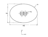
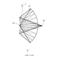
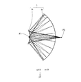
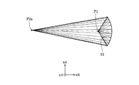
- FIG. 1 shows schematically the structure of the exposure apparatus concerning embodiment of this invention. It is a figure which illustrates schematically one scanning exposure in this embodiment. It is a figure which shows schematically the structure of the 1st fly eye optical member in an optical integrator. It is a figure which shows schematically the structure of the 2nd fly eye optical member in an optical integrator. It is a 1st figure which shows schematically the structure of the collector optical member concerning this embodiment. It is a 2nd figure which shows schematically the structure of the collector optical member concerning this embodiment. It is a figure which shows schematically the structure of the exposure apparatus concerning a modification. It is a 1st figure which shows roughly the structure of the collector optical member concerning a modification.
- FIG. 1 is a drawing schematically showing a configuration of an exposure apparatus according to an embodiment of the present invention.
- the Z-axis is along the normal direction of the surface (exposure surface) of the wafer W, which is a photosensitive substrate
- the Y-axis is parallel to the paper surface of FIG.
- the X axis is set in the direction perpendicular to the paper surface of FIG.
- exposure light is supplied from a light source apparatus that includes a DPP (Discharge ProducedlasPlasma) type light source unit LU and a collector optical member 1.
- DPP Discharge ProducedlasPlasma
- DPP type light source unit LU when a voltage is applied between electrodes in a state where an electrode made of a target material or a target material exists between the electrodes, a discharge occurs between the electrodes when a certain voltage is exceeded, and the target material is Turn into plasma. This discharge causes a large current to flow between the electrodes, and the plasma itself is compressed into a minute space by the magnetic field generated by this current, raising the plasma temperature. EUV light is emitted from this high temperature plasma.
- a light source that supplies (excites) energy to plasma by discharge and emits EUV light is generally called a DPP light source.
- the collector optical member 1 includes a concave reflecting mirror 1a having a through hole formed in the center and a convex reflecting mirror 1b having a through hole formed in the center in the order of incidence of light from the light source unit LU.
- the concave reflecting mirror 1a as the first reflecting mirror has a concave reflecting surface toward the light source unit LU
- the convex reflecting mirror 1b as the second reflecting mirror is a convex reflecting surface toward the concave reflecting mirror 1a.
- the divergent light emitted from the light emitting point P1 of the light source unit LU enters the concave reflecting mirror 1a through the through hole of the convex reflecting mirror 1b.
- the light reflected by the reflecting surface of the concave reflecting mirror 1a is reflected by the reflecting surface of the convex reflecting mirror 1b and then condensed at the point P2 through the through hole of the concave reflecting mirror 1a. That is, the collector optical member 1 reflects and collects the light from the light source unit LU, and forms a primary image of the light source at the position of the point P2.
- the EUV light once condensed at the point P2 passes through a pinhole member (not shown) disposed in the vicinity of the point P2, and then passes through a collimator optical member 2 having a concave reflecting mirror shape to become a substantially parallel light beam. Shaped into a second region on the surface.
- the EUV light shaped into the second region is incident from an incident surface of a fly-eye optical member 31 provided on a predetermined surface, and is guided to an optical integrator 3 including a pair of fly-eye optical members 31 and 32.
- the configuration and operation of the fly-eye optical members 31 and 32 will be described later.
- a substantial surface light source (pupil intensity distribution) having a predetermined shape is formed in the vicinity of the exit surface of the optical integrator 3, that is, in the vicinity of the reflection surface of the second fly's eye optical member 32 (the position of the illumination pupil).
- the light from the substantial surface light source passes through the deflecting member 4 having a planar reflecting surface and the condenser optical system 5 having the shape of a concave reflecting mirror, and is then emitted from the illumination optical system IL (1 to 5).
- the position of the illumination pupil of the illumination optical system IL where the above substantial surface light source is formed is the position of the entrance pupil of the projection optical system PL, which will be described later, or a position optically conjugate with the entrance pupil of the projection optical system PL. is there.
- the light emitted from the illumination optical system IL passes through an arc-shaped opening (light transmitting portion) of a field stop (not shown) disposed substantially parallel to and in close proximity to the reflective mask (reticle) M. Then, an arcuate superimposed illumination region (first region) is formed on the pattern surface of the mask M. For example, a circuit pattern for a device is formed on the mask M as a pattern to be transferred.
- the illumination optical system IL forms a pupil intensity distribution composed of a substantial surface light source on the illumination pupil by the light from the light source unit LU, and Koehler illuminations the pattern on the mask M with the light from the pupil intensity distribution.
- the mask M is held by a mask stage MS that can move along the Y direction so that the pattern surface extends along the XY plane.
- the movement of the mask stage MS is measured by a laser interferometer (not shown) having a known configuration.
- the light from the illuminated pattern of the mask M forms an image of the mask pattern on the wafer W, which is a photosensitive substrate, via the reflective projection optical system PL. That is, on the wafer W, as will be described later, for example, an arcuate still exposure region (effective exposure region) that is symmetrical with respect to the Y axis is formed.
- the projection optical system PL includes a first reflective imaging optical system that forms an intermediate image of the mask M pattern, and an image of the intermediate image of the mask pattern (secondary image of the pattern of the mask M) on the wafer W. And a second reflection imaging optical system to be formed.
- the first reflective imaging optical system is composed of four reflecting mirrors MR1 to MR4, and the second reflective imaging optical system is composed of two reflecting mirrors MR5 and MR6.
- the projection optical system PL is an optical system telecentric on the wafer side (image side).
- the wafer W is held by a wafer stage WS that can move two-dimensionally along the X and Y directions such that the exposure surface extends along the XY plane.
- the movement of the wafer stage WS is measured by a laser interferometer (not shown) having a known configuration.
- scanning exposure scan exposure
- the pattern of the mask M is transferred to one rectangular shot area of the wafer W.
- the movement speed of the wafer stage WS is set to 1/4 of the movement speed of the mask stage MS, and synchronous scanning is performed.
- the pattern of the mask M is sequentially transferred to each shot area of the wafer W by repeating scanning exposure while moving the wafer stage WS stepwise in two dimensions along the X direction and the Y direction.
- the mask is moved in the Y direction, but the mask may be moved (running obliquely) in a direction oblique to the Y direction.
- FIG. 2 is a diagram schematically illustrating one scanning exposure in the present embodiment.
- an arcuate static exposure region ER that is symmetric with respect to the Y axis corresponds to the arcuate effective imaging region and effective illumination region of the projection optical system PL.
- An arc-shaped first region which is formed on the surface of W and is also symmetrical with respect to the Y axis is formed on the pattern surface of the mask M.
- the Y direction corresponds to the normal direction of the arc-shaped side passing through the center of the arc-shaped outer shape of the first region and the static exposure region ER
- the X direction corresponds to the direction perpendicular to the Y direction. Yes.
- the arc-shaped exposure region ER is shown from the scanning start position indicated by the solid line in the drawing. It moves to the scanning end position indicated by the middle broken line.
- the first fly's eye optical member 31 includes a plurality of first mirror elements (first optical elements) 31a as shown in FIG.
- the plurality of first mirror elements 31a have the form of a concave reflecting mirror, and are arranged in parallel on a predetermined surface at a position optically conjugate with the pattern surface of the mask M, which is the irradiated surface of the illumination optical system IL.
- the second fly's eye optical member 32 includes a plurality of second mirror elements (second optical elements) 32a.
- the plurality of second mirror elements 32a have a concave reflecting mirror shape, and are arranged in parallel so as to optically correspond one-to-one with the plurality of first mirror elements 31a.
- the x1 direction is set in the direction corresponding to the X direction on the incident surface of the first fly's eye optical member 31, and the y1 direction is set in the direction orthogonal to the x1 direction on the incident surface.
- the incident surface of the first fly's eye optical member 31 is an area occupied by the reflecting surfaces of the plurality of first mirror elements 31a within a predetermined surface.
- the x2 direction is set in the direction corresponding to the X direction on the incident surface of the second fly's eye optical member system 32, and the y2 direction is set in the direction orthogonal to the x2 direction on the incident surface. .
- the incident surface of the second fly's eye optical member 32 is a region occupied by the reflective surfaces of the plurality of second mirror elements 32a within a predetermined surface. That is, the y1 and y2 directions in FIGS. 3 and 4 correspond to the scanning direction (Y direction) of the mask M and the wafer W. In FIG. 3 and FIG. 4, only a part of a large number of mirror elements 31 a and 32 a constituting the pair of fly-eye optical members 31 and 32 is shown for the sake of clarity.
- the first fly-eye optical member 31 is configured by vertically and horizontally arranging first mirror elements 31a having an arcuate outer shape. That is, the first mirror elements 31a are arranged side by side in the y1 direction so that the arc-shaped sides are adjacent to each other, and are arranged side by side in the x1 direction so that both ends of the arc-shaped are adjacent to each other. As described above, the first mirror element 31a has an arcuate outer shape on the mask M corresponding to the arcuate effective imaging region and effective illumination region of the projection optical system PL. This is because the first region having the shape is formed, and consequently the arc-shaped still exposure region ER is formed on the wafer W.
- the optical element having the outer shape corresponding to the first region can be an optical element having the arcuate outer shape.
- the outer shape of at least one optical element has a shape similar to the outer shape of the first region, a shape different from the outer shape of the first region, a posture, a curvature, an aspect ratio in the X direction and the Y direction, and the like.
- the first region and the optical element are not limited to having an arcuate outer shape.
- the optical element having the outer shape corresponding to the first region can be an optical element having the rectangular outer shape.
- the outer shape of the optical element has a shape similar to the outer shape of the first region, a shape different from the outer shape of the first region, the posture, the curvature, the aspect ratio in the X direction and the Y direction, and the like.
- the outer shape of the first region may be different from the outer shape of the optical element.
- the outer shape of the optical element is rectangular, and the illumination light reflected by the optical element is a first region having an arc-shaped outer shape by an optical system provided between the optical element and the first region.
- the optical element may be configured to form In addition, it is possible to illuminate the first region having various shapes and to use an optical element having an outer shape corresponding to the first region.
- the second fly's eye optical member 32 is configured by vertically and horizontally arranging second mirror elements 32a having a rectangular outer shape close to a square shape, for example. That is, the second mirror elements 32a are arranged side by side in the x2 direction and the y2 direction so that the rectangular sides are adjacent to each other.
- the reason why the second mirror element 32a has a rectangular outer shape close to a square shape is that a substantially circular small light source is formed on the surface of each second mirror element 32a or in the vicinity thereof.
- the outer shape of the second mirror element 32a is not limited to a square shape or a rectangular shape, but may be a polygonal shape (triangle to octagon, etc.) other than a quadrangle. Further, in order to minimize the loss of light amount, a shape that can be laid down (an optical element can be arranged without a gap) is preferable.
- the envelope of the assembly of the first element mirrors 31a of each of the first fly-eye optical members 31 has an elliptical shape, as will be described later, a light beam incident on the optical integrator 3 (that is, the first fly-eye optics). This is because the cross-sectional shape of the light beam incident on the member 31 is elliptical, and the illumination efficiency is increased.
- the envelope of the assembly of the second element mirrors 32a of each of the second fly's eye optical members 32 has a shape close to a circular shape because the exit surface of the optical integrator 3 (that is, the second fly's eye optical member). This is because the outer shape of the pupil intensity distribution (substantial surface light source) formed on the illumination pupil in the vicinity of (32 exit surfaces) is substantially circular.
- the envelope of the assembly of the first element mirrors 31a is not limited to an elliptical shape, but may be any shape having a length in the x1 direction longer than the length in the y1 direction.
- the first element mirror 31a may be arranged so as to draw envelopes having various shapes such as a rectangular shape, a polygonal shape, and an ellipse.
- the envelope of the assembly of the second element mirrors 32a is not limited to a shape close to a circular shape, and for example, envelopes of various shapes such as a perfect circle, an ellipse, an ellipse, a rectangle, and a polygon can be drawn.
- the second element mirror 32a may be disposed.
- the light beam incident on the optical integrator 3 is divided into wavefronts by the plurality of first mirror elements 31a in the first fly's eye optical member 31.
- the light beam reflected by each first mirror element 31 a is incident on the corresponding second mirror element 32 a in the second fly-eye optical member 32.
- the light beam reflected by each second mirror element 32a illuminates the arc-shaped first region on the mask M in a superimposed manner via the deflecting member 4 and the condenser optical system 5 as a light guide optical system.
- the light from the light source unit LU is led back to the mask M after being folded between the first fly-eye optical member 31 and the second fly-eye optical member 32.
- Light incident on the first fly's eye optical member 31 is not blocked by the second fly's eye optical member 32, and light emitted from the second fly's eye optical member 32 is blocked by the first fly's eye optical member 31.
- the first fly-eye optical member 31 and the second fly-eye optical member 32 face each other so that light cannot enter vertically, and a certain amount of lateral deviation occurs along the plane of FIG. Therefore, it is necessary to make the light incident obliquely.
- the second mirror element 32a constituting the second fly's eye optical member 32 moves the first mirror element 31a constituting the first fly's eye optical member 31 in an oblique direction (on the incident surface of the second fly's eye optical member 32).
- the direction is inclined with respect to the normal direction.
- the first mirror element 31a appears distorted when viewed from the second mirror element 32a.
- each of the plurality of second mirror elements 32a projects the corresponding first mirror element 31a onto the pattern surface of the mask M, which is the irradiated surface, but due to the effect of looking at the first mirror element 31a from this oblique direction,
- the image of the first mirror element 31a projected onto the mask M does not have a shape that is exactly similar to the first mirror element 31a.
- each arc-shaped illumination field formed on the pattern surface of the mask M by the plurality of light fluxes divided by the plurality of first mirror elements 31a is formed outside the desired first arc-shaped region, so-called A light amount loss due to an overlap error of the illumination field occurs.
- the optical integrator 3 divides the light flux into a plurality of light fluxes, and superimposes the plurality of light fluxes on the irradiated surface (for example, the pattern surface of the mask M and eventually the exposure surface of the wafer W), thereby illuminance in the first region. It is an optical element that makes the distribution uniform. Therefore, the optical integrator 3 can include a required number of optical elements (for example, mirror elements 31a and 32a) necessary for homogenization.
- the equalization is relatively independent in the vertical direction (for example, y1 direction, y2 direction) and the horizontal direction (for example, x1 direction, x2 direction), a predetermined number of rows in both the horizontal direction and the vertical direction are used. There may be a number of optical elements.
- the number of rows in the x1 direction of the mirror elements 31a in the first fly-eye optical member 31 is n.
- the envelope of the assembly of the first element mirrors 31a of each first fly-eye optical member 31 is circular and its diameter is Df.
- the dimension of the mirror element 31a in the x1 direction is Df / n.
- the number n of columns in the x1 direction is better for increasing the uniformity, and can be 5 or more.
- the interval between the first fly's eye optical member 31 and the second fly's eye optical member 32 is Ff, and the envelope of the assembly of the second element mirrors 32a of each of the second fly's eye optical members 32 has a circular shape. It is assumed that the diameter is Dp.
- Fc be the focal length of the light guiding optical system interposed between the second fly's eye optical member 32 and the mask M, that is, the focal length of the condenser optical system 5.
- the distance from the second fly's eye optical member 32 to the mask M can be Fc.
- Expression (1) corresponds to the fact that each mirror element 31a of the first fly's eye optical member 31 and the pattern surface of the mask M are optically conjugate and the imaging magnification thereof is Fc / Ff.
- equations (1) and (2) are modified as shown in the following equations (4) and (5). Further, when Expressions (4) and (5) are substituted into Expression (3), the relationship shown in the following Expression (6) is obtained.
- Equation (6) it is clear how to reduce the value of I on the left side.
- the number n of columns in the x1 direction of the mirror element 31a in the first fly's eye optical member 31 may be reduced.
- the number n of columns is a variable that is rather desired to be increased for sufficient homogeneity from the standpoint of optical design, and cannot be reduced.
- Wi and NAi are treated as constants as described above.
- the only variables remaining on the right side of Expression (6) are the distance Ff between the pair of fly-eye optical members 31 and 32 and the focal length Fc of the condenser optical system 5.
- the focal length Fc of the condenser optical system 5 in order to reduce the value of I, the focal length Fc of the condenser optical system 5 must be set large and the interval Ff should be set large according to the increasing rate larger than the focal length Fc.
- the diameter Df of the first fly's eye optical member 31 is increased.
- the diameter Dp of the second fly's eye optical member 32 becomes large.
- the size of the optical integrator 3 is increased, and as a result, the illumination optical system IL is increased in size. Furthermore, recently, in order to improve the resolving power in the EUV exposure apparatus, it has been studied to set the numerical aperture NAi of the light beam incident on the mask M to be larger. As is clear from the equation (6), when the numerical aperture NAi is further increased, the value of I on the left side is also increased, and the optical integrator 3 is further increased in size.
- the envelope of the assembly of the first element mirrors 31a of each of the first fly-eye optical members 31 has a major axis Dfx in the x1 direction and a minor axis Dfy in the y1 direction. Is set to an elliptical shape.
- the above equations (1), (3) and (4) are rewritten as shown in the following equations (1A), (3A) and (4A).
- Wi ⁇ (Dfx / n) ⁇ (Fc / Ff) (1A) (Dfy + Dp) / Ff I (3A) Dfx ⁇ Wi ⁇ n ⁇ (Ff / Fc) (4A)
- the envelope of the assembly of the first element mirrors 31a of each first fly-eye optical member 31 has a shape close to a circular shape because the spread angle of the divergent light supplied from the light source is shifted in the direction. This is because the light beam incident on the first fly's eye optical member 31 has a circular cross section.
- the size of the fly-eye optical members 31 and 32 is increased by setting the envelope of the assembly of the first element mirrors 31a of each first fly-eye optical member 31 to an elongated shape in the x1 direction. Without this, the value of the left side I of the equation (6A) can be reduced.
- the envelope of the assembly of the first element mirrors 31a may be an ellipse that is elongated in the x1 direction.
- the illumination efficiency at the first fly's eye optical member 31 can be maintained high.
- a light beam having a circular cross section emitted from the light emitting point P1 of the light source unit LU (a light beam having a constant light spread angle regardless of the direction) is converted into a light beam having a cross section elongated in the x1 direction.
- the collector optical member 1 may be configured to be incident on the first fly's eye optical member 31.
- the cross section of the light beam incident on the first fly's eye optical member 31 from the collector optical member 1 can have an elliptical shape elongated in the x1 direction.
- the illumination optical system IL of the present embodiment it is necessary to suppress the occurrence of distortion without increasing the size of the optical integrator 3, and to suppress the occurrence of light loss due to the overlap error of the illumination field and to have high light efficiency.
- the mask M can be illuminated under the following illumination conditions.
- the exposure apparatus of the present embodiment uses the illumination optical system IL that illuminates the mask M under the required illumination conditions with low light amount loss and high light efficiency, and performs good exposure under good illumination conditions. It can be carried out.
- the exposure apparatus uses the illumination optical system IL that includes the optical integrator 3 that suppresses the loss of light quantity and illuminates the mask M under the required illumination conditions with high light efficiency. With this, good exposure can be performed.
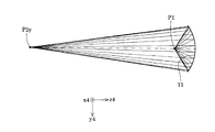
- FIGS. 5 and 6 are diagrams schematically showing the configuration of the collector optical member according to the present embodiment.
- the x3 direction and the y3 direction are set in directions corresponding to the x1 direction and the y1 direction on the incident surface (second region) of the first fly's eye optical member 31, and are perpendicular to the x3 direction and the y3 direction.
- the z3 direction is set as the direction. That is, the y3 direction in FIGS. 5 and 6 corresponds to the Y direction which is the scanning direction, and the x3 direction corresponds to the X direction orthogonal to the scanning direction.
- FIG. 5 shows light rays along the x3z3 plane
- FIG. 6 shows light rays along the y3z3 plane.
- Table (1) lists the values of the specifications of the collector optical member according to this embodiment. Table (1) is described according to the format of “Code V”, which is optical design software of ORA (Optical Research Associates).
- RDY is the radius of curvature of the surface (in the case of an aspherical surface, the radius of curvature of the vertex; unit: mm)
- THI is the distance from the surface to the next surface, that is, the surface interval (unit: mm)
- RMD indicates whether the surface is a reflective surface or a refractive surface.
- REFL means a reflective surface.
- INFINITY means infinity, and if RDY is INFINITY, it means that the surface is a plane.
- OBJ indicates a light emitting point P1
- STO indicates a virtual aperture stop surface
- IMG indicates a condensing point P2.
- Surface number 1 represents a virtual surface
- surface number 2 represents a reflecting surface of a concave reflecting mirror 1a as a first reflecting mirror
- surface number 4 represents a reflecting surface of a convex reflecting mirror 1b as a second reflecting mirror.
- SPS ZRN means that the reflecting surfaces of the reflecting mirrors 1a and 1b are aspherical surfaces represented by power series. The part other than the expression of the aspherical surface in the notation of Table (1) is the same in Table (2) described later.
- the divergent light emitted from the light emitting point P1 has a constant and circular cross section with the spread angle not depending on the direction.
- the divergent light having a circular cross section passes through the aspherical reflecting surface of the concave reflecting mirror 1a and the aspherical reflecting surface of the convex reflecting mirror 1b, and has a major axis in the x3 direction and a minor axis in the y3 direction. Is converted into a light beam having an elliptical cross section and is condensed at a point P2.
- the light beam incident on the first fly's eye optical member 31 via the condensing point P2 has an elliptical cross section having a major axis in the x1 direction and a minor axis in the y1 direction.
- the ratio of the major axis to the minor axis of the cross section of the light beam incident on the first fly's eye optical member 31 is 2: 1.
- the DPP type light source unit LU is used.
- the present invention is not limited to this.
- a modification using an LPP (Laser Produced Plasma) type light source unit LU ' is also possible.
- the LPP type light source unit LU ' the laser light is condensed on the target, and the target is turned into plasma to obtain EUV light.
- FIG. 7 has a configuration similar to that of the embodiment of FIG.
- the modification of FIG. 7 uses an LPP type light source unit LU ′ instead of the DPP type light source unit LU, and also uses a collector optical member 11 having a configuration corresponding to the LPP type light source unit LU ′.
- this is different from the embodiment of FIG.
- the configuration and operation of the modified example of FIG. 7 will be described with a focus on differences from the embodiment of FIG.
- the light source device includes a light source unit LU ′ and a collector optical member 11.
- the light source unit LU ′ includes a laser light source 21, a condenser lens 22, a nozzle 23 and a duct 24.
- a high-pressure gas made of, for example, xenon (Xe) is supplied from the nozzle 23, and the gas injected from the nozzle 23 forms the gas target 25.
- light (non-EUV light) emitted from the laser light source 21 is condensed on the gas target 25 via the condenser lens 22.
- the gas target 25 obtains energy from the focused laser beam, turns it into plasma, and emits EUV light. That is, the position of the gas target 25 becomes the light emission point P1.
- the EUV light emitted from the light emitting point P1 of the light source unit LU ′ is collected by the collector optical member 11 having a form similar to an elliptic concave reflecting mirror, and then the first fly-eye optical member via the collimator optical member 2 To 31.
- the gas that has finished emitting light is sucked through the duct 24 and guided to the outside.
- FIGS. 8 and 9 are diagrams schematically showing the configuration of the collector optical member according to the modification shown in FIG. 8 and 9, the x4 direction and the y4 direction are set in the direction corresponding to the x1 direction and the y1 direction on the incident surface (light receiving surface) of the first fly's eye optical member 31, and the directions perpendicular to the x4 direction and the y4 direction are set.
- Z4 direction is set in That is, the y4 direction in FIGS. 8 and 9 corresponds to the Y direction, which is the scanning direction, and the x3 direction corresponds to the X direction orthogonal to the scanning direction.
- FIG. 8 shows light rays along the x4z4 plane, and
- FIG. 9 shows light rays along the y4z4 plane.
- the following table (2) lists the values of the specifications of the collector optical member according to the modification.
- the “data in x4 direction” column contains data related to the light beam along the x4z4 plane in FIG. 8
- the “data in y4 direction” column contains data related to the light beam along the y4z4 plane in FIG.
- OBJ represents the light emitting point P1
- surface number 1 represents the virtual surface
- STO represents the reflecting surface of the concave reflecting mirror constituting the collector optical member 11
- IMG represents the condensing points P2x and P2y.
- ASP means an aspherical surface represented by a power series.
- the intersection of the reflecting surface of the concave reflecting mirror constituting the collector optical member 11 and the plane passing through the light emitting point P1 and parallel to the x4z4 plane is the light emitting point P1.
- the intersection line between the reflecting surface of the collector optical member 11 and a plane passing through the light emitting point P1 and parallel to the y4z4 plane has one focal point at the light emitting point P1 and is at the point P2y. It corresponds to a part of an ellipse having the other focal point.
- the divergent light supplied from the light emitting point P1 has a constant and circular cross section with the spread angle not depending on the direction.
- the light beam along the x4z4 plane is condensed at the point P2x through the aspherical reflecting surface of the collector optical member 11, and the light beam along the y4z4 plane is collected by the collector optical member 11.
- the light is condensed at a point P2y that is further from the collector optical member 11 than the point P2x through the aspherical reflecting surface.
- the divergent light having a circular cross section from the light emitting point P1 passes through the aspherical reflecting surface of the collector optical member 11, and has an elliptical cross section having a major axis in the x4 direction and a minor axis in the y4 direction. Is converted into a luminous flux having
- the light beam incident on the first fly's eye optical member 31 has an elliptical cross section having a major axis in the x1 direction and a minor axis in the y1 direction.
- the ratio of the major axis to the minor axis of the cross section of the light beam incident on the first fly's eye optical member 31 is 1.1: 1.
- the collector optical member 11 reflects and collects the light from the light source unit LU 'to form a primary image of the light source.
- the light collection point P2x along the x4z4 plane does not match the light collection point P2y along the y4z4 plane.
- the light beam propagating in the y4z4 plane is the light emitting point (that is, the light source) of the light source unit LU ′.
- a light beam that is condensed at a condensing position P2y between P1 and the mask M and propagates in the x4z4 plane is condensed at a condensing position P2x between the light emitting point P1 of the light source unit LU ′ and the condensing position P2y.
- the light condensed at the light condensing position P2y between the light emitting point P1 of the light source unit LU ′ and the mask M constitutes the collector optical member 11 out of the light from the light source unit LU ′. It propagates through the y4z4 cross section of the condensing surface of the concave reflecting mirror. At the same time, the light condensed at the condensing position P2x between the light emitting point P1 of the light source unit LU 'and the condensing position P2y propagates through the x4z4 cross section of the condensing surface.
- the curvature of the condensing surface is different between the y4z4 cross section including the y4 direction and the x4z4 cross section including the x4 direction (cross section orthogonal to the y4z4 cross section).
- the curvature radius of the x4z4 cross section is larger than the curvature radius of the y4z4 cross section on the light collecting surface.
- the light condensed on the condensing surface of the x4z4 cross section of the collector optical member 11 is optical between the collector optical member 11 and the superimposed illumination region (first region) on the mask M.
- the direction projected onto the superimposed illumination area by the system (2 to 5) is the X direction.
- the direction in which the light condensed on the condensing surface of the collector optical member 11 on the y4z4 cross section is projected onto the superimposed illumination area by the optical system (2 to 5) is the Y direction.
- the plurality of first mirror elements 31a of the first fly's eye optical member 31 and the plurality of second mirror elements 32a of the second fly's eye optical member 32 correspond optically.
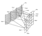
- “optically corresponds” means that, for example, as shown in FIG. 10, light reflected by one mirror element 31a among the plurality of first mirror elements 31a is out of the plurality of second mirror elements 32a. It is reflected by any one of the mirror elements 32a. Specifically, in FIG. 10, light reflected by the first mirror elements 31a1, 31a2, 31a3, 31a4, and 31a5 is incident on the second mirror elements 32a1, 32a2, 32a3, 32a4, and 32a5, respectively.
- the first mirror element 31a1 and the second mirror element 32a1 correspond optically.
- the first mirror elements 31a2 to 31a5 and the second mirror elements 32a2 to 32a5 optically correspond to each other.
- the plurality of first mirror elements 31a and the plurality of second mirror elements 32a do not have to have a one-to-one correspondence, and the light reflected by one first mirror element is reflected by another first mirror element. Light may be reflected by the same second mirror element. Alternatively, there may be a second mirror element that does not reflect the light reflected by the first mirror element.
- the optical correspondence between the plurality of first mirror elements and the plurality of second mirror elements may be changed.
- the intensity distribution in the cross section of the light beam incident on the first fly's eye optical member 31 is elliptical
- the intensity distribution in the cross section (pupil plane) of the light beam incident on the second fly's eye optical member 32 is circular. can do.
- the intensity distribution on the pupil plane is not limited to a circular shape, and may be a bipolar shape, a quadrupole shape, an annular zone, a rectangular shape, an elliptical shape, or the like. Even in such a case, the resolving power of the pattern formed on the wafer W can be made equal in two orthogonal directions (for example, the X direction and the Y direction). At this time, the optical correspondence between the plurality of first mirror elements and the plurality of second mirror elements may be adjusted.
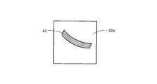
- the outer shape of the light source image 41 is astigmatism due to the influence of the cross-sectional shape of the light beam divided by the first fly's eye optical member 31 (that is, the influence of the anisotropy of the curvature of the condensing surface of the collector optical member 11). Therefore, the other becomes longer with respect to one direction. There is no particular problem as long as the light source image 41 (that is, the light beam incident on the second mirror element 32a) does not protrude from the reflection surface of the second mirror element 32a. However, if the light source image 41 is too large and protrudes from the reflection surface of the second mirror element 32a, not only light amount loss occurs but also an illumination field overlap error in the superimposed illumination region on the mask M occurs. .
- the number of wavefront divisions in the first fly-eye optical member 31 tends to increase, that is, the reflection of the first mirror element 31a and the second mirror element 32a.
- the surface tends to be downsized.
- the second mirror element 32a is downsized, the light source image 41 protrudes from the reflection surface of the second mirror element 32a, and there is a high possibility that the light amount loss and the collapse of the superimposed illumination area will occur.
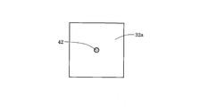
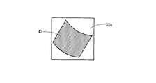
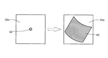
- the size of the light source image 42 formed on the second mirror element 32a is reduced by making the reflecting surface of the first mirror element 31a into a toroidal surface as schematically shown in FIG. Suppressing and thus avoiding the loss of light quantity and the collapse of the superimposed illumination area.
- the reflection surface of the first mirror element 31a is formed in a toroidal surface shape in which the curvature of the surface along the x1 direction and the curvature of the surface along the y1 direction are different from each other.
- the light source image 41 elongated in one direction obtained when the reflecting surface of the first mirror element 31a has a spherical shape becomes a light source image 42 having a relatively small size that is not defocused as a whole.
- a required curvature along the x1 direction and a required curvature along the y1 direction are given to the reflection surface of the first mirror element 31a.
- the curvature along the x1 direction and the curvature along the y1 direction of the reflection surface of the first mirror element 31a are different from each other.
- the multilayer film forming the reflection surface of the second mirror element 32a may be easily deformed or damaged by light irradiation.
- the image 43 can be positively formed, and thermal deformation and damage of the multilayer film can be reduced.
- the curvature Cx4 along the y4 direction of the condensing surface of the concave reflecting mirror constituting the collector optical member 11 is, for example, 5: 6 or 7: 8.
- the curvature Cy1 along the x1 direction of the reflection surface of the first mirror element 31a may be set to 5: 6, 6: 5, 7: 8, 8: 7, for example. it can.
- the curvature Cy4: curvature Cx4 in the collector optical member 11 is 5: 6
- the curvature Cx1: curvature Cy1 of the first mirror element 31a is 5: 6
- the size is relatively small on the second mirror element 32a.
- a light source image 42 is obtained, and as a result, it is possible to avoid the loss of light amount and the collapse of the superimposed illumination area.
- curvature Cy4: curvature Cx4 in the collector optical member 11 is 5: 6
- the curvature Cx1: curvature Cy1 of the first mirror element 31a is 7: 8
- the size is relatively large on the second mirror element 32a.
- a light source image 43 is obtained, and as a result, thermal deformation and damage of the multilayer film can be reduced.
- the influence of the curvature of the condensing surface of the collector optical member 11 and the reflection surface of the first mirror element 31a on the illumination efficiency on the mask M is different from the curvature of the collector optical member 11 and the first mirror.
- the correction can be performed by adjusting the relationship with the curvature of the element 31a
- the reflecting surface of the second mirror element 32a may remain spherical. If correction is not possible even if the curvature relationship between the collector optical member 11 and the first mirror element 31a is adjusted, the correction can be made by forming the reflecting surface of the second mirror element 32a into a required toroidal surface shape.
- the reflecting surfaces of all the first mirror elements 31a it is not necessary to make the reflecting surfaces of all the first mirror elements 31a to be a toroidal surface, and the required number (at least one) of reflecting surfaces of the first mirror elements 31a is formed in a toroidal surface.
- the effect of avoiding the occurrence of light loss and the collapse of the superimposed illumination region, or the effect of reducing the thermal deformation and damage of the multilayer film can be obtained.
- These effects are obtained when the curvature Cx1 along the x1 direction and the curvature Cy1 along the y1 direction of the reflecting surface of the first mirror element 31a satisfy the following conditional expression (7), for example.
- the technique of making the reflecting surface of the first mirror element 31a a toroidal surface is applied to the configuration of the modification of FIG.
- the present invention is not limited to the configuration of the modified example of FIG. 7, and the method of making the reflecting surface of the first mirror element 31 a toroidal can also be applied to the configuration of the embodiment of FIG. 1.
- the light condensing point P2 of the light from the collector optical member 1 coincides without depending on the direction.
- a light source image 42 having a relatively small size is formed on the reflection surface of the second mirror element 32a, and the multilayer film is thermally deformed or damaged by light irradiation. May be easier to do.
- the curvature Cx1 along the x1 direction and the curvature Cy1 along the y1 direction of the reflection surface of the first mirror element 31a are appropriately adjusted, so that the diagram on the right side of FIG.
- the light source image 43 having a relatively large size which is defocused as a whole can be positively formed, and thermal deformation and damage of the multilayer film can be reduced.
- a region is formed on the pattern surface of the mask M.
- the optical device of the first form is disposed in the optical path between the light source unit LU (LU ′) and the mask M, condenses the light from the light source unit LU (LU ′), and is in the y1 direction (Y direction).
- a second region (an elliptical incident light beam region having a major axis in the x1 direction and a minor axis in the y1 direction) that is longer in the x1 direction (corresponding to the X direction) than the length of A first fly having a collector optical member 1 (11) to be formed and a plurality of first mirror elements 31a provided in a predetermined plane including the second region and guiding the light of the collector optical member 1 (11) to the first region.
- the optical device of the second form is provided in the optical path between the light source unit LU (LU ′) and the mask M, and is longer in the x1 direction (corresponding to the X direction) than in the y1 direction (corresponding to the Y direction).
- a plurality of first mirror elements 31a having a long outer shape are arranged on a predetermined surface, and the first fly-eye optical system has different lengths in the y1 direction and the x1 direction of the aggregate of the arranged first mirror elements 31a
- a member 31 and a second mirror element 32a provided in the optical path between the first fly's eye optical member 31 and the mask M and having a plurality of second mirror elements 32a installed so as to optically correspond to the first mirror element 31a. 2 fly-eye optical member 32.
- the optical device of the third form is provided in a predetermined plane including a second region (an elliptical incident light beam region having a major axis in the x1 direction and a minor axis in the y1 direction), and a plurality of first mirror elements 31a.
- the 1st fly eye optical member 31 which has is provided.
- At least one of the plurality of first mirror elements 31a includes a curvature of a surface along the y1 direction (third direction) and a x1 direction (fourth direction) among surfaces orthogonal to the second region.
- first optical element constituting the first fly's eye optical member when the first optical element constituting the first fly's eye optical member is a reflecting member, optical surfaces having different curvatures in two directions are a reflecting surface, a diffractive surface, and the like.
- first optical element when the first optical element is a light transmission member, optical surfaces having different curvatures in two directions are a lens surface, a diffraction surface, and the like.
- the occurrence of distortion is suppressed without causing an increase in the size of the optical integrator 3, and thus the occurrence of light amount loss due to the illumination field overlap error is suppressed and the light efficiency is reduced.
- the mask M can be illuminated under a high required illumination condition.
- the illumination optical system IL that illuminates the mask M under the required illumination condition that suppresses the light amount loss and has high light efficiency is used. With this, good exposure can be performed.
- the second region an elliptical incident light beam region having a major axis in the x1 direction and a minor axis in the y1 direction; a region of the incident light beam on the first fly's eye optical member 31
- You may comprise so that the length of x1 direction may be 1.1 times or more longer than the length of y1 direction.
- the aspect ratio between the length in the y1 direction and the length in the x1 direction in the second region is 1: ⁇ , it may be configured to satisfy the condition that ⁇ is 1.1 or more. Further, ⁇ can be set to 4.0 or less.
- the mirror elements 31a of the optical integrator 3 it is possible to further reduce the light loss by configuring the mirror elements 31a of the optical integrator 3 to be arranged only in the second region.
- ⁇ when the aspect ratio between the length in the y3 direction and the length in the x1 direction in the aggregate of the mirror elements 31a is 1: ⁇ , ⁇ may be configured to satisfy the condition of 1.1 or more. Further, ⁇ can be set to 4.0 or less.
- the length in the x1 direction is 1.1 times or more than the length in the y1 direction in the cross section of the light beam incident on the optical integrator 3 (and hence the light beam incident on the first fly's eye optical member 31). You may comprise so that it may be long. Further, when the aspect ratio between the length in the y1 direction and the length in the x1 direction in the cross-section of the light beam incident on the optical integrator 3 is 1: ⁇ , it may be configured to satisfy the condition that ⁇ is 1.1 or more. Further, ⁇ can be set to 4.0 or less.
- an illumination area that is long in the X direction intersecting the Y direction that is, an arc-shaped illumination area that is elongated in the X direction is formed on the pattern surface of the mask M.
- the first fly's eye optical member 31 in the optical integrator 3 has a mirror element 31a having an outer shape corresponding to the illumination area, that is, an arcuate outer shape elongated in the x1 direction (corresponding to the X direction) in the y1 direction (Y direction). Corresponding) and a plurality of arrangements in the x1 direction.
- the lengths in the y1 direction and the x1 direction of the aggregate of the arranged mirror elements 31a are different from each other.
- the length of the light receiving surface (incident surface) of the first fly's eye optical member 31 is different between the y1 direction and the x1 direction.
- the number of arrangements in the y1 direction and the x1 direction on the light receiving surface of the first fly's eye optical member 31 are different from each other.
- the optical optical system IL that illuminates the mask M under the required illumination conditions with high light efficiency which includes the optical integrator 3 that suppresses the light loss, is good. Good exposure can be performed under various illumination conditions.
- the aspect ratio between the y1 direction and the x1 direction of the aggregate of the arranged mirror elements 31a is 1: ⁇ , it may be configured such that ⁇ satisfies the condition of 1.1 or more. Further, the aggregate of the arranged mirror elements 31a may be configured to be 1.1 times or longer in the x1 direction with respect to the y1 direction. Moreover, you may comprise so that the aggregate
- the collimator optical system 2 is provided between the collector optical member 1 and the optical integrator 3, but the present invention is not limited to this. That is, light from the light source unit LU (LU ′) enters the first fly's eye optical member 31 of the optical integrator 3 without passing through an optical member having power (for example, an optical member such as the collimator optical system 2). You may comprise so that it may do.
- the power of the optical member is the reciprocal of the focal length of the optical member.
- an exposure apparatus including a projection optical system in which the entrance pupil is located on the projection optical system side with respect to the object plane (corresponding to the pattern surface of the mask M) is referred to as a normal pupil type exposure apparatus.
- the present invention is not limited to the normal pupil type exposure apparatus and can be applied to the reverse pupil type exposure apparatus.
- An exposure apparatus having a projection optical system in which the entrance pupil is located on the opposite side of the projection optical system with the object plane in between is called an inverted pupil type exposure apparatus.
- the inverted pupil type exposure apparatus light from the light source unit LU (LU ′) passes through the collector optical member 1 (collector optical member 11) and then passes through the collimator optical system 2 in the illumination optical system IL. Is incident on the optical integrator 3. Thereafter, the light that has passed through the optical integrator 3 forms an arc-shaped first region on the mask M via an oblique incidence mirror (planar reflecting mirror). That is, the light passing through the second fly's eye optical member 32 of the optical integrator 3 does not pass through an optical member having power (for example, an optical member such as the condenser optical system 5), and the pattern surface of the mask M as an irradiated surface. Led to.
- an optical member having power for example, an optical member such as the condenser optical system 5
- An optical member having power may be interposed in the optical path between the optical integrator 3 and the irradiated surface. Moreover, it is good also as a structure which does not interpose the optical member which has power like the collimator optical system 2 between the collector optical member 1 (11) and the optical integrator 3.
- FIG. 1 A structure which does not interpose the optical member which has power like the collimator optical system 2 between the collector optical member 1 (11) and the optical integrator 3.
- the first mirror element 31a in the first fly's eye optical member 31 has an arcuate outer shape
- the second mirror element 32a in the second fly's eye optical member 32 has a rectangular outer shape. Has a shape.
- the present invention is not limited to this, and various forms are possible for the outer shape of each optical element and the power of each optical element.
- a refractive optical element or a diffractive optical element can be used instead of the mirror element.
- the ratio of the major axis to the minor axis of the cross section of the light beam incident on the first fly's eye optical member 31 is 2: 1 or 1.1: 1.
- the ratio of the major axis to the minor axis of the cross section of the incident light beam is not limited to this, and can be ⁇ : 1 (where ⁇ is 1.1 or more). Further, ⁇ may be 4.0 or less.
- the light from the light source unit LU has a first region that is longer in the X direction than the length in the Y direction, that is, an arcuate overlapping illumination region that is elongated in the X direction. , Formed on the pattern surface of the mask M.
- the light from the light source is condensed and guided to the second region on the predetermined surface, and the length in the fourth direction intersecting the third direction is longer than the length in the third direction on the predetermined surface.
- the method includes dividing the wavefront into a plurality of light beams having a long outer shape, and guiding the plurality of light beams obtained by wavefront division to the first region.
- the second region has a shape in which the length in the fourth direction is longer than the length in the third direction (incident light flux region that is long in the x1 direction and short in the y1 direction), and a plurality of light fluxes on the predetermined plane are A plurality are arranged along the three directions and the fourth direction.
- the optical device used for uniformly illuminating an illumination area having a length in the X direction longer than a length in the Y direction by light from the light source unit LU (LU ′).
- the light from the light source is condensed, and the second region (long in the x1 direction and short in the y1 direction) having a length in the fourth direction intersecting the third direction is longer than the length in the third direction.
- the optical device used for uniformly illuminating an illumination region having a length in the X direction longer than a length in the Y direction by light from the light source unit LU (LU ′).
- a plurality of first optical elements having an outer shape whose length in the fourth direction intersecting the third direction is longer than the length in the third direction; and
- the assembly of the first optical elements arranged in the three directions and the fourth direction includes obtaining first fly-eye optical members that are different from each other in the length in the third direction and the length in the fourth direction.
- variable pattern forming apparatus that forms a predetermined pattern based on predetermined electronic data can be used.
- a spatial light modulation element including a plurality of reflection elements driven based on predetermined electronic data
- An exposure apparatus using a spatial light modulator is disclosed in, for example, US Patent Publication No. 2007/0296936.
- a transmissive spatial light modulator may be used, or a self-luminous image display element may be used.
- the exposure apparatus of the above-described embodiment is manufactured by assembling various subsystems including the respective constituent elements recited in the claims of the present application so as to maintain predetermined mechanical accuracy, electrical accuracy, and optical accuracy. Is done. To ensure these various accuracies, before and after this assembly, various optical systems are adjusted to achieve optical accuracy, various mechanical systems are adjusted to achieve mechanical accuracy, and various electrical systems are Adjustments are made to achieve electrical accuracy.
- the assembly process from the various subsystems to the exposure apparatus includes mechanical connection, electrical circuit wiring connection, pneumatic circuit piping connection and the like between the various subsystems. Needless to say, there is an assembly process for each subsystem before the assembly process from the various subsystems to the exposure apparatus. When the assembly process of the various subsystems to the exposure apparatus is completed, comprehensive adjustment is performed to ensure various accuracies as the entire exposure apparatus.
- the exposure apparatus may be manufactured in a clean room where the temperature, cleanliness, etc. are controlled.
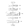
- FIG. 15 is a flowchart showing a manufacturing process of a semiconductor device.
- a metal film is vapor-deposited on a wafer W to be a semiconductor device substrate (step S40), and a photoresist, which is a photosensitive material, is applied on the vapor-deposited metal film.
- Step S42 the pattern formed on the mask (reticle) M is transferred to each shot area on the wafer W (step S44: exposure process), and the transfer of the wafer W after the transfer is completed.
- step S46 development process
- step S48 processing step
- the resist pattern is a photoresist layer in which unevenness having a shape corresponding to the pattern transferred by the exposure apparatus of the above-described embodiment is generated, and the recess penetrates the photoresist layer. is there.
- the surface of the wafer W is processed through this resist pattern.
- the processing performed in step S48 includes, for example, at least one of etching of the surface of the wafer W or film formation of a metal film or the like.
- the exposure apparatus of the above-described embodiment performs pattern transfer using the wafer W coated with the photoresist as a photosensitive substrate.
- the present invention is applied to an exposure apparatus having a light source for supplying EUV light.
- the present invention is not limited to this, and a light source that supplies light of a wavelength other than EUV light.
- the present invention can also be applied to an exposure apparatus having
- the present invention is applied to the illumination optical system of the EUV exposure apparatus that uses the reflective mask M.
- the present invention is not limited to this, and the first embodiment is based on the light from the light source.
- the present invention can also be applied to a general illumination optical system that illuminates one area.
Landscapes
- Physics & Mathematics (AREA)
- General Physics & Mathematics (AREA)
- Optics & Photonics (AREA)
- Exposure Of Semiconductors, Excluding Electron Or Ion Beam Exposure (AREA)
- Exposure And Positioning Against Photoresist Photosensitive Materials (AREA)
- Microscoopes, Condenser (AREA)
- Lenses (AREA)
Abstract
Description
前記光源と前記第1領域との間の光路中に配置されて、前記光源からの光を集光して、第3方向の長さよりも前記第3方向と交差する第4方向の長さが長い第2領域を所定面に形成するコレクター光学部材と、
前記第2領域を含む所定面内に設けられ、前記コレクター光学部材の光を前記第1領域に導く複数の第1光学要素を有する第1フライアイ光学部材と、
を備えることを特徴とする光学装置を提供する。
前記光源と前記第1領域との間の光路中に設けられ、第3方向の長さより前記第3方向と交差する第4方向の長さが長い外形形状を有する第1光学要素を、所定面に複数配列するとともに、配列された前記第1光学要素の集合体の前記第3方向と前記第4方向の長さが互いに異なる第1フライアイ光学部材と、
前記第1フライアイ光学部材と前記第1領域との間の光路中に設けられ、前記第1光学要素に光学的に対応するように設置された複数の第2光学要素を有する第2フライアイ光学部材と、
を備えることを特徴とする光学装置を提供する。
第2領域を含む所定面内に設けられ、複数の第1光学要素を有する第1フライアイ光学部材を備え、
前記複数の第1光学要素のうちの少なくとも一つの光学要素が、前記第2領域と直交する面のうちで、第3方向に沿った面の曲率と、前記第3方向と交差する第4方向に沿った面の曲率とが互いに異なる光学面を有することを特徴とする光学装置を提供する。
前記所定のパターンを感光性基板に露光することを特徴とする露光装置を提供する。
前記所定のパターンが転写された前記感光性基板を現像し、前記所定のパターンに対応する形状のマスク層を前記感光性基板の表面に形成する現像工程と、
前記マスク層を介して前記感光性基板の表面を加工する加工工程と、
を含むことを特徴とするデバイス製造方法を提供する。
光を発生する発光部と、
前記発光部で発生した光を集光して、第3方向の長さよりも前記第3方向と交差する第4方向の長さが長い第2領域を前記所定面内に形成するコレクター光学部材と、を備えることを特徴とする光源装置を提供する。
所定面上の第2領域に前記光源からの光を集光して導くことと;
前記所定面上で第3方向の長さより前記第3方向と交差する第4方向の長さが長い外形形状を有する複数の光束に波面分割することと;
該波面分割された複数の光束を前記第1領域へ導くことと;
を含み、
前記第2領域は、前記第3方向の長さよりも前記第4方向の長さが長い形状を有し、
前記所定面上での前記複数の光束は、前記第3方向と前記第4方向とに沿って複数配列されることを特徴とする照明方法を提供する。
前記所定のパターンを感光性基板に露光することと;
を含むことを特徴とする露光方法を提供する。
前記所定のパターンが転写された前記感光性基板を現像し、前記所定のパターンに対応する形状のマスク層を前記感光性基板の表面に形成することと;
前記マスク層を介して前記感光性基板の表面を加工することと;
を含むことを特徴とするデバイス製造方法を提供する。
前記光源からの光を集光して、第3方向の長さよりも前記第3方向と交差する第4方向の長さが長い第2領域を所定面に形成するコレクター光学部材を得ることと;
前記第2領域を含む所定面内に、複数の第1光学要素を有する第1フライアイ光学部材を設置することと;
を備えることを特徴とする光学装置の製造方法を提供する。
第3方向の長さより前記第3方向と交差する第4方向の長さが長い外形形状を有する複数の第1光学要素を準備することと;
前記複数の第1光学要素を前記第3方向と前記第4方向とに配列する前記第1光学要素の集合体が、前記第3方向の長さと前記第4方向の長さとで互いに異なる第1フライアイ光学部材を得ることと;
を備える光学装置の製造方法を提供する。
Wi≒(Df/n)×(Fc/Ff) (1)
NAi≒Dp/(2×Fc) (2)
(Df+Dp)/Ff=I (3)
Dp≒NAi×(2×Fc) (5)
I≒Wi×n/Fc+2×NAi×(Fc/Ff) (6)
Wi≒(Dfx/n)×(Fc/Ff) (1A)
(Dfy+Dp)/Ff=I (3A)
Dfx≒Wi×n×(Ff/Fc) (4A)
I≒(Wi×n/Fc)/m+2×NAi×(Fc/Ff) (6A)
RDY THI RMD GLA
OBJ: INFINITY 0.000000
1: INFINITY 1500.000124
2: -432.83272 -949.999641 REFL
SPS ZRN:
SCO
K: -9.4341E-01 ZP4: -1.8270E-05 ZP5: 4.3276E-04
ZP11: 4.3260E-13 ZP12: -1.9463E-12 ZP13: 1.0935E-11
ZP22: -2.6779E-20 ZP23: -6.7188E-20 ZP24: -7.5913E-20
ZP25: 4.5844E-19 ZP38: -2.9880E-29 ZP39: -3.1230E-27
ZP40: 2.1408E-26 ZP41: 2.6357E-27 ZP56: 1.1351E-33
ZP57: -1.6723E-33 ZP58: -3.4764E-34 ZP59: 7.2244E-34
ZP60: -4.0069E-33 ZP61: 3.9159E-33
STO: INFINITY -500.000000
4: -0.00000 1800.000000 REFL
SPS ZRN:
SCO
K: -1.4290E+33 ZP4: -2.5757E-04 ZP5: -1.9264E-04
ZP11: -3.4980E-11 ZP12: 3.1541E-12 ZP13: 4.8114E-11
ZP22: -8.3924E-17 ZP23: 6.3352E-17 ZP24: 3.2097E-17
ZP25: -5.6027E-17 ZP38: 7.4668E-23 ZP39: -5.3416E-24
ZP40: 1.9365E-23 ZP41: 5.7693E-23 ZP56: 2.3481E-28
ZP57: 3.9143E-29 ZP58: 1.4709E-30 ZP59: 2.1537E-29
ZP60: 8.3116E-30 ZP61: -1.0180E-29
IMG: INFINITY 0.000000
<x4方向のデータ>
RDY THI RMD GLA
OBJ: INFINITY 0.000000
1: INFINITY 150.000000
STO: -256.06602 -874.264069 REFL
ASP:
K : -0.500000
IC : YES CUF: 0.000000
A :0.000000E+00 B :0.000000E+00 C :0.000000E+00 D :0.000000E+00
IMG: INFINITY 0.000000
<y4方向のデータ>
RDY THI RMD GLA
OBJ: INFINITY 0.000000
1: INFINITY 150.000000
STO: -266.18950 -1180.947502 REFL
ASP:
K : -0.600000
IC : YES CUF: 0.000000
A :0.000000E+00 B :0.000000E+00 C :0.000000E+00 D :0.000000E+00
IMG: INFINITY 0.000000
1.0<Cx1/Cy1<1.2または1.0<Cy1/Cx1<1.2 (7)
2 コリメータ光学部材
3 オプティカルインテグレータ
5 コンデンサー光学系
31,32 フライアイ光学部材
LU,LU’ 光源ユニット
M マスク
MS マスクステージ
PL 投影光学系
W ウェハ
WS ウェハステージ
Claims (52)
- 光源からの光により第1方向の長さよりも前記第1方向と交差する第2方向の長さが長い第1領域を照明する光学装置において、
前記光源と前記第1領域との間の光路中に配置されて、前記光源からの光を集光して、第3方向の長さよりも前記第3方向と交差する第4方向の長さが長い第2領域を所定面に形成するコレクター光学部材と、
前記第2領域を含む所定面内に設けられ、前記コレクター光学部材の光を前記第1領域に導く複数の第1光学要素を有する第1フライアイ光学部材と、
を備えることを特徴とする光学装置。 - 前記第1フライアイ光学部材と前記第1領域との間の光学系によって前記第3方向が前記第1領域に射影される方向が前記第1方向であるとともに、前記第4方向が射影される方向が前記第2方向であることを特徴とする請求項1に記載の光学装置。
- 前記コレクター光学部材は、
前記第2領域における前記第3方向の長さよりも、前記第4方向の長さが、1.1倍以上長い光を形成することを特徴とする請求項1または2に記載の光学装置。 - 前記コレクター光学部材は、
前記第2領域における前記第3方向の長さと前記第4方向の長さとのアスペクト比が、1:αとすると、αが1.1以上の条件を満たす光を形成することを特徴とする請求項1または2に記載の光学装置。 - 前記コレクター光学部材は、
前記光源からの光を集光する集光面の曲率が、第1断面と前記第1断面に直交する第2断面とで異なることを特徴とする請求項1乃至4のいずれか1項に記載の光学装置。 - 前記コレクター光学部材は、
前記光源からの光を反射して集光することを特徴とする請求項1乃至5のいずれか1項に記載の光学装置。 - 前記コレクター光学部材は、
前記光源の一次像を形成することを特徴とする請求項1乃至6のいずれか1項に記載の光学装置。 - 前記コレクター光学部材は、
非球面状で且つ凹面状の反射面および貫通孔を有する第1反射鏡と、
前記光源と前記第1反射鏡との間の光路中に配置されて、非球面状で且つ凸面状の反射面および貫通孔を有する第2反射鏡と、を備え、
前記光源からの光を、前記第2反射鏡の貫通孔、前記第1反射鏡の反射面、前記第2反射鏡の反射面、および前記第1反射鏡の貫通孔を介して、前記第2領域に整形させることを特徴とする請求項1乃至7のいずれか1項に記載の光学装置。 - 前記第1光学要素は、
前記第3方向の長さと前記第4方向の長さとが異なる外形形状を有し、
前記所定面内の前記第3方向と前記第4方向とに沿って配列されることを特徴とする請求項1乃至8のいずれか1項に記載の光学装置。 - 前記第1光学要素は、
前記第3方向の長さより前記第4方向の長さが長い外形形状を有し、
前記第1光学要素の集合体は、前記第3方向より前記第4方向に長いことを特徴とする請求項9に記載の光学装置。 - 前記第1フライアイ光学部材と前記第1領域との間の光路中に設けられ、前記複数の第1光学要素に光学的に対応するように設置された複数の第2光学要素を有する第2フライアイ光学部材を、さらに備えることを特徴とする請求項1乃至10のいずれか1項に記載の光学装置。
- 前記第1フライアイ光学部材は、
前記複数の第1光学要素のうちの少なくとも1つの光学要素が、前記第2領域と直交する面のうちで、前記第3方向に沿った面の曲率と、前記第4方向に沿った面の曲率とが互いに異なる光学面を有することを特徴とする請求項1乃至11のいずれか1項に記載の光学装置。 - 前記光学面の前記第3方向に沿った面の曲率C1と前記第4方向に沿った面の曲率C2とは、
1.0<C1/C2<1.2または1.0<C2/C1<1.2
の条件を満足することを特徴とする請求項12に記載の光学装置。 - 光源からの光により第1方向の長さよりも前記第1方向と交差する第2方向の長さが長い第1領域を照明するために用いられる光学装置において、
前記光源と前記第1領域との間の光路中に設けられ、第3方向の長さより前記第3方向と交差する第4方向の長さが長い外形形状を有する第1光学要素を、所定面に複数配列するとともに、配列された前記第1光学要素の集合体の前記第3方向と前記第4方向の長さが互いに異なる第1フライアイ光学部材と、
前記第1フライアイ光学部材と前記第1領域との間の光路中に設けられ、前記第1光学要素に光学的に対応するように設置された複数の第2光学要素を有する第2フライアイ光学部材と、
を備えることを特徴とする光学装置。 - 前記第1フライアイ光学部材と前記第1領域との間の光学系によって前記第3方向が射影される方向が前記第1方向であるとともに、前記第4方向が射影される方向が前記第2方向であることを特徴とする請求項14に記載の光学装置。
- 前記第1フライアイ光学部材は、
前記第3方向に沿って配列される前記第1光学要素の数と、前記第4方向に沿って配列される前記第1光学要素の数が互いに異なるように、配列することを特徴とする請求項14または15に記載の光学装置。 - 前記第1光学要素が円弧状の外形形状を有するとともに、
前記第2光学要素が多角形状の外形形状を有することを特徴とする請求項14乃至16のいずれか1項に記載の光学装置。 - 前記第1領域は、円弧状の外形形状を有し、
前記第1方向は、前記円弧状の辺が互いに隣り合うように前記複数の第1光学要素が設置される方向に対応し、
前記第2方向は、前記円弧状の両端が互いに隣り合うように前記複数の第1光学要素が設置される方向に対応していることを特徴とする請求項17に記載の光学装置。 - 前記第1フライアイ光学部材は、
配列された前記第1光学要素の集合体の前記第3方向と前記第4方向とのアスペクト比が1:αとすると、αが1.1以上の条件を満たすことを特徴とする請求項14乃至18のいずれか1項に記載の光学装置。 - 前記第1フライアイ光学部材は、
配列された前記第1光学要素の集合体が、前記第3方向に対して前記第4方向に1.1倍以上長いことを特徴とする請求項14乃至19のいずれか1項に記載の光学装置。 - 前記第1フライアイ光学部材は、
前記第1光学要素の集合体が、前記第3方向に20列以上、前記第4方向に5列以上配列されることを特徴とする請求項14乃至20のいずれか1項に記載の光学装置。 - 前記複数の第1光学要素および前記複数の第2光学要素が、凹面反射鏡の形態を有することを特徴とする請求項14乃至21のいずれか1項に記載の光学装置。
- 前記光源と前記第1フライアイ光学部材との間の光路中に配置されて、前記光源からの光を集光して、所定面に前記第3方向の長さよりも前記第4方向の長さが長い第2領域を形成するコレクター光学部材をさらに備え、
前記複数の第1光学要素は、前記所定面内に配置されることを特徴とする請求項14乃至22のいずれか1項に記載の光学装置。 - 前記第1フライアイ光学部材は、
前記複数の第1光学要素のうちの少なくとも1つの光学要素が、前記第2領域と直交する面のうちで、前記第3方向に沿った面の曲率と、前記第4方向に沿った面の曲率とが互いに異なる光学面を有することを特徴とする請求項14乃至23のいずれか1項に記載の光学装置。 - 前記光学面の前記第3方向に沿った面の曲率C1と前記第4方向に沿った面の曲率C2とは、
1.0<C1/C2<1.2または1.0<C2/C1<1.2
の条件を満足することを特徴とする請求項24に記載の光学装置。 - 光源からの光により第1方向の長さよりも前記第1方向と交差する第2方向の長さが長い第1領域を照明するために用いられる光学装置において、
第2領域を含む所定面内に設けられ、複数の第1光学要素を有する第1フライアイ光学部材を備え、
前記複数の第1光学要素のうちの少なくとも一つの光学要素が、前記第2領域と直交する面のうちで、第3方向に沿った面の曲率と、前記第3方向と交差する第4方向に沿った面の曲率とが互いに異なる光学面を有することを特徴とする光学装置。 - 前記光学面の前記第1方向に沿った面の曲率C1と前記第2方向に沿った面の曲率C2とは、
1.0<C1/C2<1.2または1.0<C2/C1<1.2
の条件を満足することを特徴とする請求項26に記載の光学装置。 - 前記第1フライアイ光学部材と前記第1領域との間の光路中に設けられ、前記第1光学要素に光学的に対応するように設置された複数の第2光学要素を有する第2フライアイ光学部材を、さらに備えることを特徴とする請求項26または27に記載の光学装置。
- 前記光源と前記第1フライアイ光学部材との間の光路中に配置されて、前記光源からの光を集光して、第3方向の長さよりも前記第3方向と交差する第4方向の長さが長い第2領域を所定面に形成するコレクター光学部材を、
さらに備えることを特徴とする請求項26乃至28のいずれか1項に記載の光学装置。 - 前記第2フライアイ光学部材は、
前記複数の第2光学要素を、第3領域の第5方向と前記第5方向と交差する第6方向とに配列しており、
前記複数の第2光学要素のうち少なくとも1つの光学要素が、前記第3領域と直交する面のうちで、前記第5方向に沿った面の曲率と、前記第6方向に沿った面の曲率とが互いに異なる光学面を有することを特徴とする請求項11乃至25、28、29のいずれか1項に記載の光学装置。 - 前記光源から供給される光は、波長が5nm乃至20nmのEUV光であることを特徴とする請求項1乃至30のいずれか1項に記載の光学装置。
- 前記第1領域に形成された所定のパターンを照明するための請求項1乃至31のいずれか1項に記載の光学装置を備え、
前記所定のパターンを感光性基板に露光することを特徴とする露光装置。 - 前記所定のパターンの像を前記感光性基板に形成する投影光学系をさらに備え、
該投影光学系に対して前記所定のパターンおよび前記感光性基板を走査方向に沿って相対移動させて、前記所定のパターンを前記感光性基板へ投影露光することを特徴とする請求項32に記載の露光装置。 - 前記走査方向は、前記第1方向に平行な方向であることを特徴とする請求項33に記載の露光装置。
- 請求項32乃至34のいずれか1項に記載の露光装置を用いて、前記所定のパターンを前記感光性基板に露光する露光工程と、
前記所定のパターンが転写された前記感光性基板を現像し、前記所定のパターンに対応する形状のマスク層を前記感光性基板の表面に形成する現像工程と、
前記マスク層を介して前記感光性基板の表面を加工する加工工程と、
を含むことを特徴とするデバイス製造方法。 - 所定面内に設けられるフライアイ光学部材に光を供給する光源装置において、
光を発生する発光部と、
前記発光部で発生した光を集光して、第3方向の長さよりも前記第3方向と交差する第4方向の長さが長い第2領域を前記所定面内に形成するコレクター光学部材と、を備えることを特徴とする光源装置。 - 前記コレクター光学部材は、
前記第2領域における前記第3方向の長さよりも、前記第4方向の長さが、1.1倍以上長い光を形成することを特徴とする請求項36に記載の光源装置。 - 前記コレクター光学部材は、
前記第2領域における前記第3方向の長さと前記第4方向の長さとのアスペクト比が、1:αとすると、αが1.1以上の条件を満たす光を形成することを特徴とする請求項36または37に記載の光源装置。 - 前記コレクター光学部材は、
前記光源からの光を集光する集光面の曲率が、第1断面と前記第1断面に直交する第2断面とで異なることを特徴とする請求項36乃至38のいずれか1項に記載の光源装置。 - 前記コレクター光学部材は、
前記光源からの光を反射して集光することを特徴とする請求項36乃至39のいずれか1項に記載の光源装置。 - 前記コレクター光学部材は、
前記光源の一次像を形成することを特徴とする請求項36乃至40のいずれか1項に記載の光源装置。 - 前記コレクター光学部材は、
非球面状で且つ凹面状の反射面および貫通孔を有する第1反射鏡と、
前記光源と前記第1反射鏡との間の光路中に配置されて、非球面状で且つ凸面状の反射面および貫通孔を有する第2反射鏡と、を備え、
前記光源からの光を、前記第2反射鏡の貫通孔、前記第1反射鏡の反射面、前記第2反射鏡の反射面、および前記第1反射鏡の貫通孔を介して、前記第2領域に整形させることを特徴とする請求項36乃至41のいずれか1項に記載の光源装置。 - 光源からの光により第1方向の長さよりも前記第1方向と交差する第2方向の長さが長い第1領域を照明する照明方法において、
所定面上の第2領域に前記光源からの光を集光して導くことと;
前記所定面上で第3方向の長さより前記第3方向と交差する第4方向の長さが長い外形形状を有する複数の光束に波面分割することと;
該波面分割された複数の光束を前記第1領域へ導くことと;
を含み、
前記第2領域は、前記第3方向の長さよりも前記第4方向の長さが長い形状を有し、
前記所定面上での前記複数の光束は、前記第3方向と前記第4方向とに沿って複数配列されることを特徴とする照明方法。 - 前記第3方向が射影される方向が前記第1方向であるとともに、前記第4方向が射影される方向が前記第2方向であることを特徴とする請求項43に記載の照明方法。
- 前記複数の光束は、
前記第3方向と前記第4方向とにおける長さが互いに異なることを特徴とする請求項43または44に記載の照明方法。 - 前記集光して導くことでは、
前記光源からの光がコレクター光学部材の第1断面によって集光されるとともに、
前記第1断面に直交し、前記第1断面とは異なる曲率を有する前記コレクター光学部材の第2断面によって集光されることを特徴とする請求項43乃至45のいずれか1項に記載の照明方法。 - 前記集光して導くことでは、
前記コレクター光学部材の前記第1断面で集光される光によって前記光源の一次像を形成することと;
前記第2断面で集光される光によって前記光源の一次像を形成することと;
を備え、
前記第1断面で集光される光を、前記光源と前記第1領域との間の第1集光位置で集光させ、且つ前記第2断面で集光される光を、前記光源と前記第1集光位置の間の第2集光位置で集光させることを特徴とする請求項46に記載の照明方法。 - 請求項43乃至47のいずれか1項に記載の照明方法を用いて所定のパターン上の前記第1領域を照明することと;
前記所定のパターンを感光性基板に露光することと;
を含むことを特徴とする露光方法。 - 請求項48に記載の露光方法を用いて、前記所定のパターンを前記感光性基板に露光することと;
前記所定のパターンが転写された前記感光性基板を現像し、前記所定のパターンに対応する形状のマスク層を前記感光性基板の表面に形成することと;
前記マスク層を介して前記感光性基板の表面を加工することと;
を含むことを特徴とするデバイス製造方法。 - 光源からの光により第1方向の長さよりも前記第1方向と交差する第2方向の長さが長い第1領域を照明するために用いられる光学装置の製造方法において、
前記光源からの光を集光して、第3方向の長さよりも前記第3方向と交差する第4方向の長さが長い第2領域を所定面に形成するコレクター光学部材を得ることと;
前記第2領域を含む所定面内に、複数の第1光学要素を有する第1フライアイ光学部材を設置することと;
を備えることを特徴とする光学装置の製造方法。 - 光源からの光により第1方向の長さよりも前記第1方向と交差する第2方向の長さが長い第1領域を照明するために用いられる光学装置の製造方法において、
第3方向の長さより前記第3方向と交差する第4方向の長さが長い外形形状を有する複数の第1光学要素を準備することと;
前記複数の第1光学要素を前記第3方向と前記第4方向とに配列する前記第1光学要素の集合体が、前記第3方向の長さと前記第4方向の長さとで互いに異なる第1フライアイ光学部材を得ることと;
を備える光学装置の製造方法。 - 複数の第2光学要素を前記第1光学要素に光学的に対応するように設置する第2フライアイ光学部材を得ること;
をさらに備えることを特徴とする請求項50または51に記載の光学装置の製造方法。
Priority Applications (18)
| Application Number | Priority Date | Filing Date | Title |
|---|---|---|---|
| JP2012509567A JP5704519B2 (ja) | 2010-04-02 | 2011-03-31 | 光源装置、光学装置、露光装置、デバイス製造方法、照明方法、露光方法、および光学装置の製造方法 |
| KR1020237039607A KR102776597B1 (ko) | 2010-04-02 | 2011-03-31 | 조명 광학계, 노광 방법 및 디바이스 제조 방법 |
| KR1020217021477A KR102397041B1 (ko) | 2010-04-02 | 2011-03-31 | 조명 광학계, 노광 방법 및 디바이스 제조 방법 |
| KR1020177029894A KR101944655B1 (ko) | 2010-04-02 | 2011-03-31 | 조명 광학계, 광학 장치, 노광 방법 및 디바이스 제조 방법 |
| EP11765727.0A EP2555228A4 (en) | 2010-04-02 | 2011-03-31 | Light source apparatus, optical apparatus, exposure apparatus, device manufacturing method, illuminating method, exposure method, and method for manufacturing optical apparatus |
| KR1020207024346A KR102277452B1 (ko) | 2010-04-02 | 2011-03-31 | 조명 광학계, 노광 방법 및 디바이스 제조 방법 |
| KR1020197002269A KR102051267B1 (ko) | 2010-04-02 | 2011-03-31 | 조명 광학계, 노광 방법 및 디바이스 제조 방법 |
| KR1020127028634A KR20130083833A (ko) | 2010-04-02 | 2011-03-31 | 광원 장치, 광학 장치, 노광 장치, 디바이스 제조 방법, 조명 방법, 노광 방법, 및 광학 장치의 제조 방법 |
| US13/639,037 US9703204B2 (en) | 2010-04-02 | 2011-03-31 | Light source apparatus, optical apparatus, exposure apparatus, device manufacturing method, illuminating method, exposure method, and method for manufacturing optical apparatus |
| EP24150668.2A EP4328647A3 (en) | 2010-04-02 | 2011-03-31 | Light source apparatus, optical apparatus, exposure apparatus, device manufacturing method, illuminating method, exposure method, and method for manufacturing optical apparatus |
| KR1020257006728A KR20250035035A (ko) | 2010-04-02 | 2011-03-31 | 조명 광학계, 노광 방법 및 디바이스 제조 방법 |
| KR1020227015373A KR102605356B1 (ko) | 2010-04-02 | 2011-03-31 | 조명 광학계, 노광 방법 및 디바이스 제조 방법 |
| KR1020197034427A KR102160046B1 (ko) | 2010-04-02 | 2011-03-31 | 조명 광학계, 노광 방법 및 디바이스 제조 방법 |
| US15/623,749 US10345708B2 (en) | 2010-04-02 | 2017-06-15 | Light source apparatus, optical apparatus, exposure apparatus, device manufacturing method, illuminating method, exposure method, and method for manufacturing optical apparatus |
| US16/431,355 US10831106B2 (en) | 2010-04-02 | 2019-06-04 | Light source apparatus, optical apparatus, exposure apparatus, device manufacturing method, illuminating method, exposure method, and method for manufacturing optical apparatus |
| US17/034,954 US11353795B2 (en) | 2010-04-02 | 2020-09-28 | Light source apparatus, optical apparatus, exposure apparatus, device manufacturing method, illuminating method, exposure method, and method for manufacturing optical apparatus |
| US17/737,610 US11934104B2 (en) | 2010-04-02 | 2022-05-05 | Light source apparatus, optical apparatus, exposure apparatus, device manufacturing method, illuminating method, exposure method, and method for manufacturing optical apparatus |
| US18/433,957 US20240176248A1 (en) | 2010-04-02 | 2024-02-06 | Light source apparatus, optical apparatus, exposure apparatus, device manufacturing method, illuminating method, exposure method, and method for manufacturing optical apparatus |
Applications Claiming Priority (4)
| Application Number | Priority Date | Filing Date | Title |
|---|---|---|---|
| US32044310P | 2010-04-02 | 2010-04-02 | |
| US32045310P | 2010-04-02 | 2010-04-02 | |
| US61/320,453 | 2010-04-02 | ||
| US61/320,443 | 2010-04-02 |
Related Child Applications (2)
| Application Number | Title | Priority Date | Filing Date |
|---|---|---|---|
| US13/639,037 A-371-Of-International US9703204B2 (en) | 2010-04-02 | 2011-03-31 | Light source apparatus, optical apparatus, exposure apparatus, device manufacturing method, illuminating method, exposure method, and method for manufacturing optical apparatus |
| US15/623,749 Continuation US10345708B2 (en) | 2010-04-02 | 2017-06-15 | Light source apparatus, optical apparatus, exposure apparatus, device manufacturing method, illuminating method, exposure method, and method for manufacturing optical apparatus |
Publications (1)
| Publication Number | Publication Date |
|---|---|
| WO2011125827A1 true WO2011125827A1 (ja) | 2011-10-13 |
Family
ID=44762765
Family Applications (1)
| Application Number | Title | Priority Date | Filing Date |
|---|---|---|---|
| PCT/JP2011/058189 Ceased WO2011125827A1 (ja) | 2010-04-02 | 2011-03-31 | 光源装置、光学装置、露光装置、デバイス製造方法、照明方法、露光方法、および光学装置の製造方法 |
Country Status (5)
| Country | Link |
|---|---|
| US (6) | US9703204B2 (ja) |
| EP (2) | EP4328647A3 (ja) |
| JP (1) | JP5704519B2 (ja) |
| KR (9) | KR102160046B1 (ja) |
| WO (1) | WO2011125827A1 (ja) |
Cited By (3)
| Publication number | Priority date | Publication date | Assignee | Title |
|---|---|---|---|---|
| KR20160118353A (ko) * | 2014-02-21 | 2016-10-11 | 칼 짜이스 에스엠티 게엠베하 | 투영 리소그래피용 조명 광학 유닛 |
| US20180142865A1 (en) * | 2013-11-15 | 2018-05-24 | Lg Innotek Co., Ltd. | Optical member and lighting device using the same |
| JP2021193456A (ja) * | 2016-05-19 | 2021-12-23 | 株式会社ニコン | 露光装置、露光方法および高密度ラインのパターニングのためのeuvリソグラフィシステム |
Families Citing this family (10)
| Publication number | Priority date | Publication date | Assignee | Title |
|---|---|---|---|---|
| KR102290738B1 (ko) | 2009-11-24 | 2021-08-18 | 가부시키가이샤 니콘 | 결상 광학계, 노광 장치 및 디바이스 제조 방법 |
| KR102160046B1 (ko) * | 2010-04-02 | 2020-09-28 | 가부시키가이샤 니콘 | 조명 광학계, 노광 방법 및 디바이스 제조 방법 |
| WO2013118615A1 (ja) * | 2012-02-06 | 2013-08-15 | 株式会社ニコン | 反射結像光学系、露光装置、およびデバイス製造方法 |
| ITRM20120265A1 (it) * | 2012-06-07 | 2013-12-08 | Consiglio Nazionale Ricerche | Dispositivo di illuminazione comprendente una schiera di sorgenti optoelettroniche |
| US9354508B2 (en) | 2013-03-12 | 2016-05-31 | Applied Materials, Inc. | Planarized extreme ultraviolet lithography blank, and manufacturing and lithography systems therefor |
| US9632411B2 (en) * | 2013-03-14 | 2017-04-25 | Applied Materials, Inc. | Vapor deposition deposited photoresist, and manufacturing and lithography systems therefor |
| US20140272684A1 (en) | 2013-03-12 | 2014-09-18 | Applied Materials, Inc. | Extreme ultraviolet lithography mask blank manufacturing system and method of operation therefor |
| KR102374206B1 (ko) | 2017-12-05 | 2022-03-14 | 삼성전자주식회사 | 반도체 장치 제조 방법 |
| US20240271996A1 (en) * | 2023-02-09 | 2024-08-15 | Kla Corporation | Optical beam sensor with center transmissive cut-out |
| KR102859739B1 (ko) | 2024-12-23 | 2025-09-16 | 신우이엔지 주식회사 | 배큠 릴리프 밸브 및 그를 구비하는 탱크 어셈블리 |
Citations (7)
| Publication number | Priority date | Publication date | Assignee | Title |
|---|---|---|---|---|
| JP2002048977A (ja) * | 2000-08-01 | 2002-02-15 | Nikon Corp | 反射光学系及びこの光学系を用いたプロキシミティ露光装置 |
| JP2004311814A (ja) * | 2003-04-09 | 2004-11-04 | Nikon Corp | 光源ユニット、照明光学装置、露光装置および露光方法 |
| JP2006253487A (ja) * | 2005-03-11 | 2006-09-21 | Nikon Corp | 照明装置、投影露光方法、投影露光装置、及びマイクロデバイスの製造方法 |
| JP2007234717A (ja) * | 2006-02-28 | 2007-09-13 | Nikon Corp | 露光装置 |
| US20070273859A1 (en) | 2006-05-25 | 2007-11-29 | Hideki Komatsuda | Illumination optical apparatus, exposure apparatus, and device manufacturing method |
| US20070296936A1 (en) | 2005-01-25 | 2007-12-27 | Nikon Corporation | Exposure Apparatus, Exposure Method, and Producing Method of Microdevice |
| JP2009054340A (ja) * | 2007-08-24 | 2009-03-12 | Seiko Epson Corp | 照明装置及びプロジェクタ |
Family Cites Families (19)
| Publication number | Priority date | Publication date | Assignee | Title |
|---|---|---|---|---|
| US5636003A (en) * | 1992-11-05 | 1997-06-03 | Nikon Corporation | Illumination optical apparatus and scanning exposure apparatus |
| JP3633002B2 (ja) * | 1994-05-09 | 2005-03-30 | 株式会社ニコン | 照明光学装置、露光装置及び露光方法 |
| US6833904B1 (en) * | 1998-02-27 | 2004-12-21 | Nikon Corporation | Exposure apparatus and method of fabricating a micro-device using the exposure apparatus |
| EP0955641B1 (de) * | 1998-05-05 | 2004-04-28 | Carl Zeiss | Beleuchtungssystem insbesondere für die EUV-Lithographie |
| DE10100265A1 (de) * | 2001-01-08 | 2002-07-11 | Zeiss Carl | Beleuchtungssystem mit Rasterelementen unterschiedlicher Größe |
| US6195201B1 (en) * | 1999-01-27 | 2001-02-27 | Svg Lithography Systems, Inc. | Reflective fly's eye condenser for EUV lithography |
| DE19931848A1 (de) * | 1999-07-09 | 2001-01-11 | Zeiss Carl Fa | Astigmatische Komponenten zur Reduzierung des Wabenaspektverhältnisses bei EUV-Beleuchtungssystemen |
| JP2003506881A (ja) * | 1999-07-30 | 2003-02-18 | カール ツァイス シュティフトゥング トレイディング アズ カール ツァイス | Euv照明光学系の射出瞳における照明分布の制御 |
| US6919951B2 (en) * | 2001-07-27 | 2005-07-19 | Canon Kabushiki Kaisha | Illumination system, projection exposure apparatus and device manufacturing method |
| US6883904B2 (en) | 2002-04-24 | 2005-04-26 | Eastman Kodak Company | Apparatus and method for maintaining constant drop volumes in a continuous stream ink jet printer |
| DE602004024168D1 (de) * | 2003-01-10 | 2009-12-31 | Nippon Kogaku Kk | Belichtungssystem und belichtungsverfahren |
| JP4322757B2 (ja) * | 2004-09-06 | 2009-09-02 | 富士フイルム株式会社 | パターン形成材料及びパターン形成方法 |
| KR20070100964A (ko) * | 2005-02-03 | 2007-10-15 | 가부시키가이샤 니콘 | 광학 적분기, 조명 광학 장치, 노광 장치, 및 노광 방법 |
| EP1708008B1 (en) * | 2005-04-01 | 2011-08-17 | Semiconductor Energy Laboratory Co., Ltd. | Beam homogenizer and laser irradition apparatus |
| WO2007045434A2 (de) * | 2005-10-18 | 2007-04-26 | Carl Zeiss Smt Ag | Kollektor für beleuchtungssysteme mit einer wellenlänge ≤ 193 nm |
| JP5241270B2 (ja) * | 2008-02-27 | 2013-07-17 | キヤノン株式会社 | 照明光学系、これを用いた露光装置及びデバイス製造方法 |
| JP5142892B2 (ja) * | 2008-09-03 | 2013-02-13 | キヤノン株式会社 | 照明光学系及び露光装置 |
| US8497977B2 (en) * | 2009-03-12 | 2013-07-30 | Nikon Corporation | Optical integrator, illumination optical system, exposure apparatus, and device manufacturing method |
| KR102160046B1 (ko) * | 2010-04-02 | 2020-09-28 | 가부시키가이샤 니콘 | 조명 광학계, 노광 방법 및 디바이스 제조 방법 |
-
2011
- 2011-03-31 KR KR1020197034427A patent/KR102160046B1/ko active Active
- 2011-03-31 EP EP24150668.2A patent/EP4328647A3/en active Pending
- 2011-03-31 KR KR1020127028634A patent/KR20130083833A/ko not_active Ceased
- 2011-03-31 US US13/639,037 patent/US9703204B2/en active Active
- 2011-03-31 KR KR1020177029894A patent/KR101944655B1/ko active Active
- 2011-03-31 KR KR1020207024346A patent/KR102277452B1/ko active Active
- 2011-03-31 KR KR1020257006728A patent/KR20250035035A/ko active Pending
- 2011-03-31 EP EP11765727.0A patent/EP2555228A4/en not_active Withdrawn
- 2011-03-31 WO PCT/JP2011/058189 patent/WO2011125827A1/ja not_active Ceased
- 2011-03-31 KR KR1020227015373A patent/KR102605356B1/ko active Active
- 2011-03-31 KR KR1020237039607A patent/KR102776597B1/ko active Active
- 2011-03-31 JP JP2012509567A patent/JP5704519B2/ja active Active
- 2011-03-31 KR KR1020197002269A patent/KR102051267B1/ko active Active
- 2011-03-31 KR KR1020217021477A patent/KR102397041B1/ko active Active
-
2017
- 2017-06-15 US US15/623,749 patent/US10345708B2/en active Active
-
2019
- 2019-06-04 US US16/431,355 patent/US10831106B2/en active Active
-
2020
- 2020-09-28 US US17/034,954 patent/US11353795B2/en active Active
-
2022
- 2022-05-05 US US17/737,610 patent/US11934104B2/en active Active
-
2024
- 2024-02-06 US US18/433,957 patent/US20240176248A1/en active Pending
Patent Citations (8)
| Publication number | Priority date | Publication date | Assignee | Title |
|---|---|---|---|---|
| JP2002048977A (ja) * | 2000-08-01 | 2002-02-15 | Nikon Corp | 反射光学系及びこの光学系を用いたプロキシミティ露光装置 |
| JP2004311814A (ja) * | 2003-04-09 | 2004-11-04 | Nikon Corp | 光源ユニット、照明光学装置、露光装置および露光方法 |
| US20070296936A1 (en) | 2005-01-25 | 2007-12-27 | Nikon Corporation | Exposure Apparatus, Exposure Method, and Producing Method of Microdevice |
| JP2006253487A (ja) * | 2005-03-11 | 2006-09-21 | Nikon Corp | 照明装置、投影露光方法、投影露光装置、及びマイクロデバイスの製造方法 |
| JP2007234717A (ja) * | 2006-02-28 | 2007-09-13 | Nikon Corp | 露光装置 |
| US20070273859A1 (en) | 2006-05-25 | 2007-11-29 | Hideki Komatsuda | Illumination optical apparatus, exposure apparatus, and device manufacturing method |
| WO2007138805A1 (ja) * | 2006-05-25 | 2007-12-06 | Nikon Corporation | 照明光学装置、露光装置、およびデバイス製造方法 |
| JP2009054340A (ja) * | 2007-08-24 | 2009-03-12 | Seiko Epson Corp | 照明装置及びプロジェクタ |
Non-Patent Citations (1)
| Title |
|---|
| See also references of EP2555228A4 |
Cited By (10)
| Publication number | Priority date | Publication date | Assignee | Title |
|---|---|---|---|---|
| US20180142865A1 (en) * | 2013-11-15 | 2018-05-24 | Lg Innotek Co., Ltd. | Optical member and lighting device using the same |
| US10767837B2 (en) * | 2013-11-15 | 2020-09-08 | Lg Innotek Co., Ltd. | Optical member and lighting device using the same |
| KR20160118353A (ko) * | 2014-02-21 | 2016-10-11 | 칼 짜이스 에스엠티 게엠베하 | 투영 리소그래피용 조명 광학 유닛 |
| JP2017507356A (ja) * | 2014-02-21 | 2017-03-16 | カール・ツァイス・エスエムティー・ゲーエムベーハー | 投影リソグラフィのための照明光学ユニット |
| JP2020074040A (ja) * | 2014-02-21 | 2020-05-14 | カール・ツァイス・エスエムティー・ゲーエムベーハー | 投影リソグラフィのための照明光学ユニット |
| KR102402946B1 (ko) * | 2014-02-21 | 2022-05-27 | 칼 짜이스 에스엠티 게엠베하 | 투영 리소그래피용 조명 광학 유닛 |
| KR20220070578A (ko) * | 2014-02-21 | 2022-05-31 | 칼 짜이스 에스엠티 게엠베하 | 투영 리소그래피용 조명 광학 유닛 |
| KR102464752B1 (ko) | 2014-02-21 | 2022-11-09 | 칼 짜이스 에스엠티 게엠베하 | 투영 리소그래피용 조명 광학 유닛 |
| JP2021193456A (ja) * | 2016-05-19 | 2021-12-23 | 株式会社ニコン | 露光装置、露光方法および高密度ラインのパターニングのためのeuvリソグラフィシステム |
| JP7160163B2 (ja) | 2016-05-19 | 2022-10-25 | 株式会社ニコン | 露光装置、露光方法および高密度ラインのパターニングのためのeuvリソグラフィシステム |
Also Published As
Similar Documents
| Publication | Publication Date | Title |
|---|---|---|
| JP5704519B2 (ja) | 光源装置、光学装置、露光装置、デバイス製造方法、照明方法、露光方法、および光学装置の製造方法 | |
| US20250013156A1 (en) | Image-forming optical system, exposure apparatus, and device producing method | |
| JP5509933B2 (ja) | オプティカルインテグレータ、照明光学系、露光装置、およびデバイス製造方法 | |
| JP5888585B2 (ja) | 反射結像光学系、露光装置、およびデバイス製造方法 | |
| JP2004170869A (ja) | 結像光学系、露光装置および露光方法 | |
| JP2011150227A (ja) | 露光装置、およびデバイス製造方法 | |
| HK1175585A (en) | Light source apparatus, optical apparatus, exposure apparatus, device manufacturing method, illuminating method, exposure method, and method for manufacturing optical apparatus | |
| JP2005072513A (ja) | 露光装置および露光方法 |
Legal Events
| Date | Code | Title | Description |
|---|---|---|---|
| 121 | Ep: the epo has been informed by wipo that ep was designated in this application |
Ref document number: 11765727 Country of ref document: EP Kind code of ref document: A1 |
|
| WWE | Wipo information: entry into national phase |
Ref document number: 2012509567 Country of ref document: JP |
|
| NENP | Non-entry into the national phase |
Ref country code: DE |
|
| ENP | Entry into the national phase |
Ref document number: 20127028634 Country of ref document: KR Kind code of ref document: A |
|
| WWE | Wipo information: entry into national phase |
Ref document number: 2011765727 Country of ref document: EP |
|
| WWE | Wipo information: entry into national phase |
Ref document number: 13639037 Country of ref document: US |
|
| WWP | Wipo information: published in national office |
Ref document number: 1020257006728 Country of ref document: KR |