WO2011126040A1 - Ptc素子と発熱体モジュール - Google Patents
Ptc素子と発熱体モジュール Download PDFInfo
- Publication number
- WO2011126040A1 WO2011126040A1 PCT/JP2011/058681 JP2011058681W WO2011126040A1 WO 2011126040 A1 WO2011126040 A1 WO 2011126040A1 JP 2011058681 W JP2011058681 W JP 2011058681W WO 2011126040 A1 WO2011126040 A1 WO 2011126040A1
- Authority
- WO
- WIPO (PCT)
- Prior art keywords
- ceramic composition
- semiconductor ceramic
- electrode
- ptc element
- temperature
- Prior art date
- Legal status (The legal status is an assumption and is not a legal conclusion. Google has not performed a legal analysis and makes no representation as to the accuracy of the status listed.)
- Ceased
Links
Images


Classifications
-
- C—CHEMISTRY; METALLURGY
- C04—CEMENTS; CONCRETE; ARTIFICIAL STONE; CERAMICS; REFRACTORIES
- C04B—LIME, MAGNESIA; SLAG; CEMENTS; COMPOSITIONS THEREOF, e.g. MORTARS, CONCRETE OR LIKE BUILDING MATERIALS; ARTIFICIAL STONE; CERAMICS; REFRACTORIES; TREATMENT OF NATURAL STONE
- C04B35/00—Shaped ceramic products characterised by their composition; Ceramics compositions; Processing powders of inorganic compounds preparatory to the manufacturing of ceramic products
- C04B35/01—Shaped ceramic products characterised by their composition; Ceramics compositions; Processing powders of inorganic compounds preparatory to the manufacturing of ceramic products based on oxide ceramics
- C04B35/46—Shaped ceramic products characterised by their composition; Ceramics compositions; Processing powders of inorganic compounds preparatory to the manufacturing of ceramic products based on oxide ceramics based on titanium oxides or titanates
- C04B35/462—Shaped ceramic products characterised by their composition; Ceramics compositions; Processing powders of inorganic compounds preparatory to the manufacturing of ceramic products based on oxide ceramics based on titanium oxides or titanates based on titanates
- C04B35/465—Shaped ceramic products characterised by their composition; Ceramics compositions; Processing powders of inorganic compounds preparatory to the manufacturing of ceramic products based on oxide ceramics based on titanium oxides or titanates based on titanates based on alkaline earth metal titanates
- C04B35/468—Shaped ceramic products characterised by their composition; Ceramics compositions; Processing powders of inorganic compounds preparatory to the manufacturing of ceramic products based on oxide ceramics based on titanium oxides or titanates based on titanates based on alkaline earth metal titanates based on barium titanates
- C04B35/4682—Shaped ceramic products characterised by their composition; Ceramics compositions; Processing powders of inorganic compounds preparatory to the manufacturing of ceramic products based on oxide ceramics based on titanium oxides or titanates based on titanates based on alkaline earth metal titanates based on barium titanates based on BaTiO3 perovskite phase
-
- C—CHEMISTRY; METALLURGY
- C04—CEMENTS; CONCRETE; ARTIFICIAL STONE; CERAMICS; REFRACTORIES
- C04B—LIME, MAGNESIA; SLAG; CEMENTS; COMPOSITIONS THEREOF, e.g. MORTARS, CONCRETE OR LIKE BUILDING MATERIALS; ARTIFICIAL STONE; CERAMICS; REFRACTORIES; TREATMENT OF NATURAL STONE
- C04B35/00—Shaped ceramic products characterised by their composition; Ceramics compositions; Processing powders of inorganic compounds preparatory to the manufacturing of ceramic products
- C04B35/01—Shaped ceramic products characterised by their composition; Ceramics compositions; Processing powders of inorganic compounds preparatory to the manufacturing of ceramic products based on oxide ceramics
- C04B35/46—Shaped ceramic products characterised by their composition; Ceramics compositions; Processing powders of inorganic compounds preparatory to the manufacturing of ceramic products based on oxide ceramics based on titanium oxides or titanates
- C04B35/462—Shaped ceramic products characterised by their composition; Ceramics compositions; Processing powders of inorganic compounds preparatory to the manufacturing of ceramic products based on oxide ceramics based on titanium oxides or titanates based on titanates
- C04B35/465—Shaped ceramic products characterised by their composition; Ceramics compositions; Processing powders of inorganic compounds preparatory to the manufacturing of ceramic products based on oxide ceramics based on titanium oxides or titanates based on titanates based on alkaline earth metal titanates
- C04B35/468—Shaped ceramic products characterised by their composition; Ceramics compositions; Processing powders of inorganic compounds preparatory to the manufacturing of ceramic products based on oxide ceramics based on titanium oxides or titanates based on titanates based on alkaline earth metal titanates based on barium titanates
- C04B35/4686—Shaped ceramic products characterised by their composition; Ceramics compositions; Processing powders of inorganic compounds preparatory to the manufacturing of ceramic products based on oxide ceramics based on titanium oxides or titanates based on titanates based on alkaline earth metal titanates based on barium titanates based on phases other than BaTiO3 perovskite phase
-
- C—CHEMISTRY; METALLURGY
- C04—CEMENTS; CONCRETE; ARTIFICIAL STONE; CERAMICS; REFRACTORIES
- C04B—LIME, MAGNESIA; SLAG; CEMENTS; COMPOSITIONS THEREOF, e.g. MORTARS, CONCRETE OR LIKE BUILDING MATERIALS; ARTIFICIAL STONE; CERAMICS; REFRACTORIES; TREATMENT OF NATURAL STONE
- C04B35/00—Shaped ceramic products characterised by their composition; Ceramics compositions; Processing powders of inorganic compounds preparatory to the manufacturing of ceramic products
- C04B35/622—Forming processes; Processing powders of inorganic compounds preparatory to the manufacturing of ceramic products
- C04B35/626—Preparing or treating the powders individually or as batches ; preparing or treating macroscopic reinforcing agents for ceramic products, e.g. fibres; mechanical aspects section B
- C04B35/62605—Treating the starting powders individually or as mixtures
- C04B35/62645—Thermal treatment of powders or mixtures thereof other than sintering
- C04B35/62675—Thermal treatment of powders or mixtures thereof other than sintering characterised by the treatment temperature
-
- C—CHEMISTRY; METALLURGY
- C04—CEMENTS; CONCRETE; ARTIFICIAL STONE; CERAMICS; REFRACTORIES
- C04B—LIME, MAGNESIA; SLAG; CEMENTS; COMPOSITIONS THEREOF, e.g. MORTARS, CONCRETE OR LIKE BUILDING MATERIALS; ARTIFICIAL STONE; CERAMICS; REFRACTORIES; TREATMENT OF NATURAL STONE
- C04B35/00—Shaped ceramic products characterised by their composition; Ceramics compositions; Processing powders of inorganic compounds preparatory to the manufacturing of ceramic products
- C04B35/622—Forming processes; Processing powders of inorganic compounds preparatory to the manufacturing of ceramic products
- C04B35/626—Preparing or treating the powders individually or as batches ; preparing or treating macroscopic reinforcing agents for ceramic products, e.g. fibres; mechanical aspects section B
- C04B35/62605—Treating the starting powders individually or as mixtures
- C04B35/62685—Treating the starting powders individually or as mixtures characterised by the order of addition of constituents or additives
-
- H—ELECTRICITY
- H01—ELECTRIC ELEMENTS
- H01C—RESISTORS
- H01C7/00—Non-adjustable resistors formed as one or more layers or coatings; Non-adjustable resistors made from powdered conducting material or powdered semi-conducting material with or without insulating material
- H01C7/02—Non-adjustable resistors formed as one or more layers or coatings; Non-adjustable resistors made from powdered conducting material or powdered semi-conducting material with or without insulating material having positive temperature coefficient
- H01C7/022—Non-adjustable resistors formed as one or more layers or coatings; Non-adjustable resistors made from powdered conducting material or powdered semi-conducting material with or without insulating material having positive temperature coefficient mainly consisting of non-metallic substances
- H01C7/023—Non-adjustable resistors formed as one or more layers or coatings; Non-adjustable resistors made from powdered conducting material or powdered semi-conducting material with or without insulating material having positive temperature coefficient mainly consisting of non-metallic substances containing oxides or oxidic compounds, e.g. ferrites
- H01C7/025—Perovskites, e.g. titanates
-
- C—CHEMISTRY; METALLURGY
- C04—CEMENTS; CONCRETE; ARTIFICIAL STONE; CERAMICS; REFRACTORIES
- C04B—LIME, MAGNESIA; SLAG; CEMENTS; COMPOSITIONS THEREOF, e.g. MORTARS, CONCRETE OR LIKE BUILDING MATERIALS; ARTIFICIAL STONE; CERAMICS; REFRACTORIES; TREATMENT OF NATURAL STONE
- C04B2235/00—Aspects relating to ceramic starting mixtures or sintered ceramic products
- C04B2235/02—Composition of constituents of the starting material or of secondary phases of the final product
- C04B2235/30—Constituents and secondary phases not being of a fibrous nature
- C04B2235/32—Metal oxides, mixed metal oxides, or oxide-forming salts thereof, e.g. carbonates, nitrates, (oxy)hydroxides, chlorides
- C04B2235/3201—Alkali metal oxides or oxide-forming salts thereof
-
- C—CHEMISTRY; METALLURGY
- C04—CEMENTS; CONCRETE; ARTIFICIAL STONE; CERAMICS; REFRACTORIES
- C04B—LIME, MAGNESIA; SLAG; CEMENTS; COMPOSITIONS THEREOF, e.g. MORTARS, CONCRETE OR LIKE BUILDING MATERIALS; ARTIFICIAL STONE; CERAMICS; REFRACTORIES; TREATMENT OF NATURAL STONE
- C04B2235/00—Aspects relating to ceramic starting mixtures or sintered ceramic products
- C04B2235/02—Composition of constituents of the starting material or of secondary phases of the final product
- C04B2235/30—Constituents and secondary phases not being of a fibrous nature
- C04B2235/32—Metal oxides, mixed metal oxides, or oxide-forming salts thereof, e.g. carbonates, nitrates, (oxy)hydroxides, chlorides
- C04B2235/3205—Alkaline earth oxides or oxide forming salts thereof, e.g. beryllium oxide
- C04B2235/3208—Calcium oxide or oxide-forming salts thereof, e.g. lime
-
- C—CHEMISTRY; METALLURGY
- C04—CEMENTS; CONCRETE; ARTIFICIAL STONE; CERAMICS; REFRACTORIES
- C04B—LIME, MAGNESIA; SLAG; CEMENTS; COMPOSITIONS THEREOF, e.g. MORTARS, CONCRETE OR LIKE BUILDING MATERIALS; ARTIFICIAL STONE; CERAMICS; REFRACTORIES; TREATMENT OF NATURAL STONE
- C04B2235/00—Aspects relating to ceramic starting mixtures or sintered ceramic products
- C04B2235/02—Composition of constituents of the starting material or of secondary phases of the final product
- C04B2235/30—Constituents and secondary phases not being of a fibrous nature
- C04B2235/32—Metal oxides, mixed metal oxides, or oxide-forming salts thereof, e.g. carbonates, nitrates, (oxy)hydroxides, chlorides
- C04B2235/3205—Alkaline earth oxides or oxide forming salts thereof, e.g. beryllium oxide
- C04B2235/3213—Strontium oxides or oxide-forming salts thereof
-
- C—CHEMISTRY; METALLURGY
- C04—CEMENTS; CONCRETE; ARTIFICIAL STONE; CERAMICS; REFRACTORIES
- C04B—LIME, MAGNESIA; SLAG; CEMENTS; COMPOSITIONS THEREOF, e.g. MORTARS, CONCRETE OR LIKE BUILDING MATERIALS; ARTIFICIAL STONE; CERAMICS; REFRACTORIES; TREATMENT OF NATURAL STONE
- C04B2235/00—Aspects relating to ceramic starting mixtures or sintered ceramic products
- C04B2235/02—Composition of constituents of the starting material or of secondary phases of the final product
- C04B2235/30—Constituents and secondary phases not being of a fibrous nature
- C04B2235/32—Metal oxides, mixed metal oxides, or oxide-forming salts thereof, e.g. carbonates, nitrates, (oxy)hydroxides, chlorides
- C04B2235/3224—Rare earth oxide or oxide forming salts thereof, e.g. scandium oxide
- C04B2235/3225—Yttrium oxide or oxide-forming salts thereof
-
- C—CHEMISTRY; METALLURGY
- C04—CEMENTS; CONCRETE; ARTIFICIAL STONE; CERAMICS; REFRACTORIES
- C04B—LIME, MAGNESIA; SLAG; CEMENTS; COMPOSITIONS THEREOF, e.g. MORTARS, CONCRETE OR LIKE BUILDING MATERIALS; ARTIFICIAL STONE; CERAMICS; REFRACTORIES; TREATMENT OF NATURAL STONE
- C04B2235/00—Aspects relating to ceramic starting mixtures or sintered ceramic products
- C04B2235/02—Composition of constituents of the starting material or of secondary phases of the final product
- C04B2235/30—Constituents and secondary phases not being of a fibrous nature
- C04B2235/32—Metal oxides, mixed metal oxides, or oxide-forming salts thereof, e.g. carbonates, nitrates, (oxy)hydroxides, chlorides
- C04B2235/3224—Rare earth oxide or oxide forming salts thereof, e.g. scandium oxide
- C04B2235/3227—Lanthanum oxide or oxide-forming salts thereof
-
- C—CHEMISTRY; METALLURGY
- C04—CEMENTS; CONCRETE; ARTIFICIAL STONE; CERAMICS; REFRACTORIES
- C04B—LIME, MAGNESIA; SLAG; CEMENTS; COMPOSITIONS THEREOF, e.g. MORTARS, CONCRETE OR LIKE BUILDING MATERIALS; ARTIFICIAL STONE; CERAMICS; REFRACTORIES; TREATMENT OF NATURAL STONE
- C04B2235/00—Aspects relating to ceramic starting mixtures or sintered ceramic products
- C04B2235/02—Composition of constituents of the starting material or of secondary phases of the final product
- C04B2235/30—Constituents and secondary phases not being of a fibrous nature
- C04B2235/32—Metal oxides, mixed metal oxides, or oxide-forming salts thereof, e.g. carbonates, nitrates, (oxy)hydroxides, chlorides
- C04B2235/3231—Refractory metal oxides, their mixed metal oxides, or oxide-forming salts thereof
- C04B2235/3232—Titanium oxides or titanates, e.g. rutile or anatase
- C04B2235/3234—Titanates, not containing zirconia
-
- C—CHEMISTRY; METALLURGY
- C04—CEMENTS; CONCRETE; ARTIFICIAL STONE; CERAMICS; REFRACTORIES
- C04B—LIME, MAGNESIA; SLAG; CEMENTS; COMPOSITIONS THEREOF, e.g. MORTARS, CONCRETE OR LIKE BUILDING MATERIALS; ARTIFICIAL STONE; CERAMICS; REFRACTORIES; TREATMENT OF NATURAL STONE
- C04B2235/00—Aspects relating to ceramic starting mixtures or sintered ceramic products
- C04B2235/02—Composition of constituents of the starting material or of secondary phases of the final product
- C04B2235/30—Constituents and secondary phases not being of a fibrous nature
- C04B2235/32—Metal oxides, mixed metal oxides, or oxide-forming salts thereof, e.g. carbonates, nitrates, (oxy)hydroxides, chlorides
- C04B2235/3231—Refractory metal oxides, their mixed metal oxides, or oxide-forming salts thereof
- C04B2235/3251—Niobium oxides, niobates, tantalum oxides, tantalates, or oxide-forming salts thereof
- C04B2235/3255—Niobates or tantalates, e.g. silver niobate
-
- C—CHEMISTRY; METALLURGY
- C04—CEMENTS; CONCRETE; ARTIFICIAL STONE; CERAMICS; REFRACTORIES
- C04B—LIME, MAGNESIA; SLAG; CEMENTS; COMPOSITIONS THEREOF, e.g. MORTARS, CONCRETE OR LIKE BUILDING MATERIALS; ARTIFICIAL STONE; CERAMICS; REFRACTORIES; TREATMENT OF NATURAL STONE
- C04B2235/00—Aspects relating to ceramic starting mixtures or sintered ceramic products
- C04B2235/02—Composition of constituents of the starting material or of secondary phases of the final product
- C04B2235/30—Constituents and secondary phases not being of a fibrous nature
- C04B2235/32—Metal oxides, mixed metal oxides, or oxide-forming salts thereof, e.g. carbonates, nitrates, (oxy)hydroxides, chlorides
- C04B2235/3294—Antimony oxides, antimonates, antimonites or oxide forming salts thereof, indium antimonate
-
- C—CHEMISTRY; METALLURGY
- C04—CEMENTS; CONCRETE; ARTIFICIAL STONE; CERAMICS; REFRACTORIES
- C04B—LIME, MAGNESIA; SLAG; CEMENTS; COMPOSITIONS THEREOF, e.g. MORTARS, CONCRETE OR LIKE BUILDING MATERIALS; ARTIFICIAL STONE; CERAMICS; REFRACTORIES; TREATMENT OF NATURAL STONE
- C04B2235/00—Aspects relating to ceramic starting mixtures or sintered ceramic products
- C04B2235/02—Composition of constituents of the starting material or of secondary phases of the final product
- C04B2235/30—Constituents and secondary phases not being of a fibrous nature
- C04B2235/32—Metal oxides, mixed metal oxides, or oxide-forming salts thereof, e.g. carbonates, nitrates, (oxy)hydroxides, chlorides
- C04B2235/3298—Bismuth oxides, bismuthates or oxide forming salts thereof, e.g. zinc bismuthate
-
- C—CHEMISTRY; METALLURGY
- C04—CEMENTS; CONCRETE; ARTIFICIAL STONE; CERAMICS; REFRACTORIES
- C04B—LIME, MAGNESIA; SLAG; CEMENTS; COMPOSITIONS THEREOF, e.g. MORTARS, CONCRETE OR LIKE BUILDING MATERIALS; ARTIFICIAL STONE; CERAMICS; REFRACTORIES; TREATMENT OF NATURAL STONE
- C04B2235/00—Aspects relating to ceramic starting mixtures or sintered ceramic products
- C04B2235/02—Composition of constituents of the starting material or of secondary phases of the final product
- C04B2235/30—Constituents and secondary phases not being of a fibrous nature
- C04B2235/34—Non-metal oxides, non-metal mixed oxides, or salts thereof that form the non-metal oxides upon heating, e.g. carbonates, nitrates, (oxy)hydroxides, chlorides
- C04B2235/3418—Silicon oxide, silicic acids or oxide forming salts thereof, e.g. silica sol, fused silica, silica fume, cristobalite, quartz or flint
-
- C—CHEMISTRY; METALLURGY
- C04—CEMENTS; CONCRETE; ARTIFICIAL STONE; CERAMICS; REFRACTORIES
- C04B—LIME, MAGNESIA; SLAG; CEMENTS; COMPOSITIONS THEREOF, e.g. MORTARS, CONCRETE OR LIKE BUILDING MATERIALS; ARTIFICIAL STONE; CERAMICS; REFRACTORIES; TREATMENT OF NATURAL STONE
- C04B2235/00—Aspects relating to ceramic starting mixtures or sintered ceramic products
- C04B2235/02—Composition of constituents of the starting material or of secondary phases of the final product
- C04B2235/50—Constituents or additives of the starting mixture chosen for their shape or used because of their shape or their physical appearance
- C04B2235/54—Particle size related information
- C04B2235/5409—Particle size related information expressed by specific surface values
-
- C—CHEMISTRY; METALLURGY
- C04—CEMENTS; CONCRETE; ARTIFICIAL STONE; CERAMICS; REFRACTORIES
- C04B—LIME, MAGNESIA; SLAG; CEMENTS; COMPOSITIONS THEREOF, e.g. MORTARS, CONCRETE OR LIKE BUILDING MATERIALS; ARTIFICIAL STONE; CERAMICS; REFRACTORIES; TREATMENT OF NATURAL STONE
- C04B2235/00—Aspects relating to ceramic starting mixtures or sintered ceramic products
- C04B2235/02—Composition of constituents of the starting material or of secondary phases of the final product
- C04B2235/50—Constituents or additives of the starting mixture chosen for their shape or used because of their shape or their physical appearance
- C04B2235/54—Particle size related information
- C04B2235/5418—Particle size related information expressed by the size of the particles or aggregates thereof
- C04B2235/5436—Particle size related information expressed by the size of the particles or aggregates thereof micrometer sized, i.e. from 1 to 100 micron
-
- C—CHEMISTRY; METALLURGY
- C04—CEMENTS; CONCRETE; ARTIFICIAL STONE; CERAMICS; REFRACTORIES
- C04B—LIME, MAGNESIA; SLAG; CEMENTS; COMPOSITIONS THEREOF, e.g. MORTARS, CONCRETE OR LIKE BUILDING MATERIALS; ARTIFICIAL STONE; CERAMICS; REFRACTORIES; TREATMENT OF NATURAL STONE
- C04B2235/00—Aspects relating to ceramic starting mixtures or sintered ceramic products
- C04B2235/02—Composition of constituents of the starting material or of secondary phases of the final product
- C04B2235/50—Constituents or additives of the starting mixture chosen for their shape or used because of their shape or their physical appearance
- C04B2235/54—Particle size related information
- C04B2235/5418—Particle size related information expressed by the size of the particles or aggregates thereof
- C04B2235/5445—Particle size related information expressed by the size of the particles or aggregates thereof submicron sized, i.e. from 0,1 to 1 micron
-
- C—CHEMISTRY; METALLURGY
- C04—CEMENTS; CONCRETE; ARTIFICIAL STONE; CERAMICS; REFRACTORIES
- C04B—LIME, MAGNESIA; SLAG; CEMENTS; COMPOSITIONS THEREOF, e.g. MORTARS, CONCRETE OR LIKE BUILDING MATERIALS; ARTIFICIAL STONE; CERAMICS; REFRACTORIES; TREATMENT OF NATURAL STONE
- C04B2235/00—Aspects relating to ceramic starting mixtures or sintered ceramic products
- C04B2235/70—Aspects relating to sintered or melt-casted ceramic products
- C04B2235/72—Products characterised by the absence or the low content of specific components, e.g. alkali metal free alumina ceramics
-
- C—CHEMISTRY; METALLURGY
- C04—CEMENTS; CONCRETE; ARTIFICIAL STONE; CERAMICS; REFRACTORIES
- C04B—LIME, MAGNESIA; SLAG; CEMENTS; COMPOSITIONS THEREOF, e.g. MORTARS, CONCRETE OR LIKE BUILDING MATERIALS; ARTIFICIAL STONE; CERAMICS; REFRACTORIES; TREATMENT OF NATURAL STONE
- C04B2235/00—Aspects relating to ceramic starting mixtures or sintered ceramic products
- C04B2235/70—Aspects relating to sintered or melt-casted ceramic products
- C04B2235/80—Phases present in the sintered or melt-cast ceramic products other than the main phase
- C04B2235/85—Intergranular or grain boundary phases
Definitions
- the present invention relates to a PTC element having a semiconductor ceramic composition having a positive resistance temperature coefficient used for a PTC (Positive Temperature Coefficient) thermistor, a PTC heater, a PTC switch, a temperature detector, and the like, and a heating element module using the PTC element About.
- PTC Physical Temperature Coefficient
- Patent Document 1 a semiconductor ceramic composition having a positive temperature coefficient of resistance is disclosed in Patent Document 1.
- Such a semiconductor ceramic composition has a characteristic that the resistance value increases abruptly when the temperature becomes higher than the Curie point, and therefore is used for a PTC thermistor, a PTC heater, a PTC switch, a temperature detector, and the like.
- PTC Positive Temperature Coefficient of Resistivity
- the present inventors made various Pb-free semiconductor ceramic compositions and evaluated their characteristics.
- the conventional semiconductor ceramic compositions regardless of whether Pb is contained or not, contain Schottky crystals.
- a semiconductor porcelain composition having a specific composition and a specific defect exhibits PTCR characteristics due to a Schottky barrier at the interface between the electrode and the semiconductor ceramic composition.
- Substances that exhibit PTCR characteristics due to the Schottky barrier at the interface between the electrode and the semiconductor ceramic composition have a large degree of freedom in element shape because the withstand voltage does not change with respect to the material shape, particularly the thickness.
- the present invention has been realized by finding that it can be processed into various shapes and applied to various apparatuses. Therefore, an object of the present invention is to provide a thin PTC element having excellent voltage resistance using a Pb-free semiconductor ceramic composition.
- a PTC element having at least two metal electrodes and a BaTiO 3 -based semiconductor ceramic composition disposed between the electrodes, In the semiconductor ceramic composition, a part of BaTiO 3 -based Ba is substituted with Bi—Na and a semiconducting element, vacancy is formed at least at the Bi site, and oxygen defects are formed in the crystal.
- a characteristic PTC element (2) The PTC element according to (1), wherein the porosity of Bi is greater than 5% and 75% or less with respect to the Bi site. (3) The PTC element according to (1) or (2), wherein the oxygen defect is 10 ppm or less with respect to the O site.
- vacancies are formed in the Na site, and the porosity of the Na is greater than 0% and less than or equal to 60% with respect to the Na site (1) ) To (3).
- vacancies are formed in the Ba site, and the porosity of the Ba is greater than 0% and 4% or less with respect to the Ba site (1) ) To (4).
- a PTC element having at least two metal electrodes and a BaTiO 3 -based semiconductor ceramic composition disposed between the electrodes, In the semiconductor ceramic composition, a part of BaTiO 3 -based Ba is substituted with Bi—Na and a semiconducting element, vacancies are formed at least at the Bi site, and oxygen defects are formed in the crystal.
- a PTC element wherein a depletion layer is present in the vicinity of an interface between the metal electrode and the semiconductor ceramic composition.
- the width of the depletion layer may be 0.04 ⁇ m to 0.8 ⁇ m.
- a heating element module comprising the PTC element according to any one of (1) to (8) and a power supply electrode provided on the PTC element.
- the PTC element of the present invention it is possible to realize a PTC element that expresses PTCR characteristics by the resistance component at the interface between the semiconductor ceramic composition and the electrode. That is, the PTCR characteristic of the PTC element of the present invention is determined by the resistance component of the interface between the semiconductor ceramic composition and the electrode, and the semiconductor ceramic composition determined by the resistance component of the crystal grain boundary inside the conventional composition. In contrast, the resistance value and jump characteristics are not determined depending on the thickness, and a thin PTC element with high withstand voltage can be obtained. Therefore, since it is not necessary to increase the thickness in order to obtain a predetermined resistance value, it is possible to realize a thin PTC element with high withstand voltage.
- FIG. 16 is a schematic diagram obtained by tracing FIG. 15 and showing the density of the depletion layer in three stages. It is a schematic diagram which shows the heating apparatus 30 using the heat generating body module of this invention. It is a perspective view which cuts out some heating element modules 12 concerning the modification of the present invention, and shows it.
- a PTC element according to the present invention is a PTC element having a plurality of electrodes and a BaTiO 3 -based semiconductor ceramic composition sandwiched between the electrodes, and an interface between the semiconductor ceramic composition and the electrodes
- the PTCR characteristic is expressed by the resistance component in the vicinity.
- a part of Ba in the BaTiO 3 based semiconductor ceramic composition is composed of Bi—Na and a semiconductor.
- the porosity of the Bi site is strongly related to the interface level concentration and is considered to affect the PTCR characteristics, the porosity of the Bi site is larger than 5% and less than 75% with respect to the Bi site. Preferably there is.
- the reason is that when the porosity of Bi is 5% or less, there is no Schottky barrier at the interface between the electrode and the PTC element and jumping is difficult, and when it exceeds 75%, the pore increases (density decreases) at room temperature. This is because the resistance increases and the evaluation itself becomes difficult.
- the porosity of Bi is more than 10%, preferably about 35% or less.
- the jump is reduced below 10%, and the room temperature resistance starts increasing above 35%.
- the porosity of Ba is greater than 0% and 4% or less with respect to the Ba site. It is preferable that the porosity of Na is greater than 0% and 60% or less with respect to the Na site. The reason is that if the porosity of Ba exceeds 4%, the number of different phases increases and it becomes difficult to make a semiconductor, and 3% or less is more preferable. When the porosity of Na exceeds 60%, different phases increase and the room temperature resistance increases, and 40% or less is more preferable.
- (BaQ) TiO 3 calcined powder (Q is a semiconducting element) is prepared.
- BaCO 3 , TiO 2 and a semiconducting element raw material powder, for example, La 2 O 3 are mixed to prepare a mixed raw material powder, which is calcined.
- the calcination temperature is preferably in the range of 900 ° C. to 1300 ° C., and the calcination time is preferably 0.5 hours or more. When the calcining temperature is less than 900 ° C. or the calcining time is less than 0.5 hour, (BaQ) TiO 3 is not completely formed, and unreacted BaO reacts with the moisture in the atmosphere and the mixed medium, causing the composition deviation. This is not preferable.
- the calcining temperature exceeds 1300 ° C.
- sintered particles are generated in the calcined powder, which is not preferable because it prevents solid solution with the (Bi—Na) TiO 3 calcined powder to be mixed later.
- BaCO 3 , TiO 2 and semiconducting element Nb 2 O 5 are mixed to prepare Ba (TiM) O 3 (M is any semiconducting element of Nb, Ta and Sb). Also good.
- the calcined powder obtained by these processes is called BT calcined powder.
- (Bi—Na) TiO 3 calcined powder is prepared. Na 2 CO 3 , Bi 2 O 3 , and TiO 2 that are raw material powders are mixed to produce a mixed raw material powder, which is calcined.
- Na 2 CO 3 and Bi 2 O 3 are mixed while being shifted from the stoichiometric composition.
- the calcining time and temperature are also controlled. For example, if Bi is blended in a substoichiometric composition, the Bi porosity increases, and if Na is blended in a smaller amount than the stoichiometric composition, the Na porosity increases.
- the calcining time for example, 4 hours on the basis of 2 hours at 800 ° C., the Bi porosity becomes about 1.1 to 1.2 times. When the temperature is 900 ° C., it becomes about 1.6 times.
- the calcining temperature is preferably in the range of 700 ° C. to 950 ° C. so that Bi is not volatilized as much as possible and there is no overreaction of Na
- the calcining time is preferably 0.5 to 10 hours.
- the calcining temperature is less than 700 ° C. or the calcining time is less than 0.5 hours, unreacted NaO reacts with moisture in the atmosphere or, in the case of wet mixing, reacts with the solvent, resulting in compositional deviation and characteristic variation. It is not preferable.
- the calcined powder obtained in this step is referred to as BNT calcined powder.
- the calcining temperature (900 ° C. to 1300 ° C.) in the step of preparing the BT calcined powder and the calcining temperature (700 ° C. to 950 ° C.) in the step of preparing the BNT calcined powder depend on the application. Also, select the optimum temperature as appropriate.
- the calcination temperature of BNT is preferably performed at a relatively low temperature by adjusting the calcination time in order to sufficiently perform the reaction while suppressing the volatilization of Bi.
- the above-described step of preparing the BT calcined powder and the step of preparing the BNT calcined powder are performed separately (divided calcining method).
- the volatilization of Bi of BNT in the calcining step can be suppressed, the composition deviation of Bi-Na can be prevented and the generation of heterogeneous phase can be suppressed, so that the room temperature resistivity is further reduced and the variation in Curie temperature is suppressed.
- a semiconductor porcelain composition can be realized.
- pulverization may be performed according to the particle size of the raw material powder when mixing the raw material powder.
- mixing and pulverization may be either wet mixing / pulverization using pure water or ethanol, or dry mixing / pulverization.
- dry mixing / pulverization is preferable because compositional deviation can be further prevented.
- raw material powders BaCO 3, Na 2 CO 3 , TiO 2 and has been raised as an example, other Ba compounds, does not impair the effects of the present invention even by using a Na compound.
- each calcined powder is mixed in a predetermined amount and then mixed.
- Mixing may be either wet mixing using pure water or ethanol or dry mixing, but it is preferable to perform dry mixing because composition deviation can be further prevented.
- pulverization after mixing, or mixing and pulverization may be performed simultaneously.
- the average particle size of the mixed calcined powder after mixing and pulverization is preferably 0.6 ⁇ m to 1.5 ⁇ m.
- the mixed calcined powder obtained by the step of mixing the BT calcined powder and the BNT calcined powder is molded by an appropriate molding means. You may granulate a pulverized powder with a granulator as needed before shaping
- the compact density after molding is preferably 2 to 3 g / cm 3 .
- the melting point of the BNT calcined powder is 1250 ° C. or higher and is stable at a high value, even if it is mixed with the BT calcined powder, firing can be performed at a higher temperature.
- One of the advantages of the divided calcining method is that it suppresses the volatilization of Bi and the overreaction of Na and uses it as BNT calcined powder having a small composition deviation of Bi—Na with respect to the weighed value.
- Sintering is performed in the air, in a reducing atmosphere, or in an inert gas atmosphere with a low oxygen concentration, at a sintering temperature of 1200 ° C. to 1400 ° C. and a sintering time of 2 hours to 6 hours.
- a binder removal treatment it is preferable to perform a binder removal treatment at 300 ° C. to 700 ° C. before sintering.
- BaTiO 3 -based semiconductor ceramic composition targeted in the present invention a part of BaTiO 3 is replaced with Bi—Na, and further, a semiconducting element is added to control the valence.
- the semiconducting element Q is added to BaTiO 3 to form (BaQ) TiO 3 calcined powder.
- the obtained semiconductor ceramic composition has the composition formula [(Bi—Na) x (Ba 1 ⁇ y Q y ) 1 ⁇ x ] TiO 3 , where x and y are 0 ⁇ x ⁇ 0.2 and 0 ⁇ y ⁇ 0. .02 is satisfied.
- the semiconductor ceramic composition represented by the above composition [(Bi—Na) x (Ba 1 ⁇ y Q y ) 1 ⁇ x ] TiO 3 , among the semiconducting elements Q, among La, Dy, Eu, Gd, and Y La is particularly preferred.
- x represents a component range of Bi + Na, and 0 ⁇ x ⁇ 0.2 is preferable. If x is 0, the Curie temperature cannot be shifted to the high temperature side, and if it exceeds 0.2, the room temperature specific resistance approaches 10 4 ⁇ ⁇ cm, making it difficult to apply to a PTC heater or the like.
- y represents a component range of Q, and 0 ⁇ y ⁇ 0.02 is preferable. This is because when y is 0, the composition does not become a semiconductor, and when it exceeds 0.02, the room temperature resistivity increases. The valence is controlled by changing the value of y. When a trivalent cation is added as a semiconducting element in a system in which a part of Ba is substituted with Bi-Na, the effect of semiconductorization is obtained. Due to the presence of monovalent Na ions, there is a problem that the room temperature resistivity increases. Therefore, a more preferable range is 0.002 ⁇ y ⁇ 0.02. The above 0.002 ⁇ y ⁇ 0.02 is 0.2 mol% to 2.0 mol% in terms of mol%.
- the composition formula is [(Bi—Na) x (Ba 1 ⁇ y Q y ) 1 ⁇ x ] TiO 3 (Q is at least one of La, Dy, Eu, Gd, and Y, and x and y are Semiconductor porcelain compositions satisfying 0 ⁇ x ⁇ 0.2 and 0 ⁇ y ⁇ 0.02 can be obtained, and these semiconductor porcelain compositions have a Curie temperature without using Pb that causes environmental pollution. The specific resistance at room temperature can be lowered.
- the semiconducting element M is Nb, Ta, Sb, and the composition formula is [(Bi—Na) x Ba 1-x ].
- [Ti 1-z M z ] O 3 (where M is at least one of Nb, Ta, and Sb), and x and z satisfy the following conditions: 0 ⁇ x ⁇ 0.2, 0 ⁇ z ⁇ 0.005
- a satisfactory composition may be used.
- the present invention can be carried out by taking means for blending the BNT calcined powder out of the stoichiometric composition.
- Raw material powders of BaCO 3 , TiO 2 , and La 2 O 3 were prepared, and these raw material powders were blended so as to be (Ba 0.994 La 0.006 ) TiO 3 .
- the blended raw material powder was mixed with pure water, and the mixed raw material powder was calcined in the atmosphere at 900 ° C. for 4 hours to obtain a BT calcined powder.
- raw material powders of Bi 2 O 3 , Na 2 CO 3 , and TiO 2 were prepared.
- ⁇ was 0.05 and ⁇ was 0.002. It mix
- the obtained mixed raw material powder was calcined in the air at 800 ° C. for 2 hours to prepare BNT calcined powder.
- the obtained BT calcined powder and BNT calcined powder are blended in a molar ratio of about 92: 8, and the center particle size of these calcined powder is 0.5 to 2.0 ⁇ m by a pot mill using pure water as a medium. Mix and grind until At this time, in order to reduce the amount of Ba in the BT calcined powder by a predetermined amount, 30 kg of BT calcined powder is ball milled in 100 l of pure water for 6 hours to dissolve Ba in pure water, and then left for 12 hours. did. When a larger amount of Ba is dissolved, the content is adjusted by stirring with a pot mill. At this time, in order to maintain the particle size of the BT calcined powder, no ball mill media is inserted.
- the mixed powder of BT calcined powder and BNT calcined powder was dried with a hot air dryer.
- PVA polyvinyl alcohol
- the obtained granulated powder was molded with a uniaxial press, the molded body was debindered at 700 ° C., and then sintered in nitrogen to obtain a sintered body.
- the porosity of Bi, Na, and Ba in the above sintered body was 18.4% for the Bi site, 6.3% for the Na site, and 2.5% for the Ba site, respectively. .
- the oxygen defect was 1 ppm with respect to the O site.
- test pieces of 10 mm ⁇ 10 mm ⁇ 1.00 mm, 10 mm ⁇ 10 mm ⁇ 0.75 mm, 10 mm ⁇ 10 mm ⁇ 10 mm ⁇ 0.5 mm, 10 mm ⁇ 10 mm ⁇ 0.25 mm were produced from the obtained sintered bodies.
- a silver-zinc electrode as an ohmic electrode and a silver electrode as a cover electrode were baked and formed on both end faces of the test piece by a screen printing method, respectively, to produce a PTC element according to the present invention.
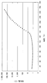
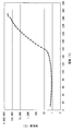
- FIG. 1 Since it can be read from FIG. 1 that the linear relationship is established between the thickness and the resistance value, an approximate straight line can be introduced into FIG.
- the resistance value R 0 (T) can be calculated at each temperature. It can also be seen that the resistance value R 0 (T) at the thickness of 0 depends on the temperature. Therefore, FIG. 2 is a plot of the resistance value R 0 (T) when the thickness is 0 for each temperature.
- the PTCR characteristic in which the resistance value suddenly increases from a predetermined temperature (in the present example, around 160 ° C.) when the thickness is theoretically 0 is obtained.
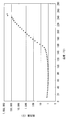
- the resistance value R 0 (T) when the thickness is 0 is considered to be due to the resistance component generated at the interface between the semiconductor ceramic composition and the electrode, not inside the semiconductor ceramic composition. This consideration can be confirmed by comparison with FIG. 3 showing the relationship between the thickness and the resistance value in the Pb-containing semiconductor ceramic composition.
- FIG. 3 shows the relationship between the temperature and resistance of a PTC element having a Pb-containing semiconductor ceramic composition.
- Pb-containing semiconductor ceramic composition Ba 0.65 Sr 0.12 Ca 0.06 Pb 0.17
- TiO 3 10 mm ⁇ 10 mm ⁇ 1.00 mm
- 10 mm ⁇ 10 mm ⁇ 0.75 mm 10 mm ⁇ 10 mm ⁇ 0.
- a plate-shaped test piece of 5 mm, 10 mm ⁇ 10 mm ⁇ 0.25 mm was prepared, the same electrode was formed on both end faces thereof to produce a PTC element, and a graph similar to FIG. 1 was created.
- a linear relationship can be established between the thickness and the resistance value, and an approximate straight line can be introduced.
- a Pb-free semiconductor ceramic composition different from the present invention is considered to have the same temperature-resistance relationship as in FIG.
- the resistance value of the semiconductor ceramic composition containing Pb increases as the thickness increases, so that jump characteristics are expressed inside the semiconductor ceramic composition. This is consistent with the fact that jump characteristics are expressed at the grain boundaries inside the semiconductor ceramic composition.
- the PTC element according to the present invention exhibits a unique phenomenon because it is assumed that the resistance value R 0 (T) exists even when the thickness of the semiconductor ceramic composition is zero. This phenomenon cannot be explained by the mechanism of the Schottky barrier formed at the crystal grain boundary.
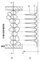
- FIG. 4A is a schematic diagram showing a state in which a Pb-containing semiconductor ceramic composition composed of a plurality of crystal grains is sandwiched between a pair of electrodes
- FIG. 4B is a diagram in FIG. It is a schematic diagram showing an energy potential E on a straight line XX.
- a curve a in FIG. 4B indicates the energy potential at room temperature
- a curve b indicates the energy potential at 200 ° C.
- FIG. 5A is a schematic view showing a state in which the semiconductor ceramic composition of the present invention composed of a plurality of crystal grains is sandwiched between a pair of electrodes
- FIG. 5B is a view in FIG.
- FIG. 6 is a schematic diagram showing an energy potential E on a straight line YY.
- a curve c in FIG. 5B shows the energy potential at room temperature
- a curve d shows the energy potential at 200 ° C.
- w in FIG. 5B indicates the width of the region showing the Schottky barrier at the interface between the electrode and the semiconductor ceramic composition.
- an energy potential is also generated at the crystal grain boundary inside the semiconductor ceramic composition, it is smaller than the energy potential at the interface between the semiconductor ceramic composition and the electrode. It can be considered that the jump characteristics are governed by the interface between the semiconductor ceramic composition and the electrode.
- FIG. 6 to FIG. 10 are obtained by examining (T). 6 to 10 calculate the resistance value R 0 (T) when the thickness at each temperature is 0 for the PTC element of 10 mm ⁇ 10 mm ⁇ 1.00 mm among the PTC elements measured in FIGS. The relationship between the temperature and the resistance value R 0 (T) of thickness 0 is shown.
- the PTC element measured in FIG. 6 is formed by sputtering a nickel electrode as an ohmic electrode and a silver electrode as a cover electrode thereon, followed by heat treatment in the atmosphere at 300 ° C. for 2 hours. .
- the PTC element measured in FIG. 7 is obtained by forming a silver electrode as a cover electrode and a nickel electrode as an ohmic electrode by sputtering, and then performing a heat treatment at 300 ° C. for 3 hours in oxygen.
- a silver electrode as a cover electrode and a nickel electrode as an ohmic electrode were formed by sputtering, and heat treatment was not performed.
- the PTC element measured in FIG. 10 is obtained by forming a nickel electrode as a cover electrode and a titanium electrode as an ohmic electrode by sputtering and performing heat treatment at 300 ° C. for 5 hours in the atmosphere.
- ⁇ Multilayer electrode structure since a resistance component is generated at the interface between the semiconductor ceramic composition and the metal electrode, the room temperature resistivity ⁇ 25 , the Curie temperature Tsc, and the resistance temperature coefficient ⁇ when the interface is increased by providing an intermediate layer electrode It was measured.
- the resistance value in the material (total resistance value) and the resistance value at the interface between the electrode and the material (resistance value R 0 (T) when thickness is 0) are separated from the measured resistance value of the semiconductor ceramic composition.
- the temperature at which the interface resistance value is twice the interface resistance value at room temperature is defined as the Curie temperature Tsc.
- Table 1 uses the PTC elements used in FIGS. 1 and 2 described above and, as shown in FIG. 11, 1 to 4 PTC elements having the same thickness are stacked, and the room temperature specific resistance ⁇ 25 of the stacked PTC elements is shown. The Curie temperature Tsc and the resistance temperature coefficient ⁇ are measured.
- a positive electrode is printed on one surface of the PTC element, a negative electrode is printed on the other surface, and the positive electrodes or negative electrodes facing the end surface of the laminate are external electrodes.
- a comb-like electrode structure connected in the above was formed.
- three sheet-like test pieces are laminated, and silver and zinc are used for the positive electrode and the negative electrode.
- the thickness of the sheet material can be about 20 to 200 ⁇ m.
- the thickness is less than 20 ⁇ m, the chemical reaction between the electrode and the material proceeds during firing and the characteristics change, which is not preferable. If it is 20 ⁇ m or more, a sheet of several hundred ⁇ m can be produced by a conventional doctor blade method or the like.
- the semiconductor porcelain composition used in this measurement was one having a Ba porosity of 2.21%, a Na porosity of 6.44%, a Bi porosity of 18.01%, and an oxygen defect rate of 1 ppm.
- the resistance temperature coefficient ⁇ is an index indicating how much the resistance value has increased before and after the jump, and the larger the value, the better the jump characteristic.
- the room temperature resistivity ⁇ 25 and the temperature coefficient of resistance ⁇ increase as the number of layers increases. Therefore, from the characteristic effect of the present invention that a high resistance value is exhibited in the vicinity of the interface, if the semiconductor ceramic composition according to the present invention is used, the number of stacked layers can be increased without changing the material and thickness of the semiconductor ceramic composition. By doing so, the PTC element can be applied to uses where high room temperature specific resistance and resistance temperature coefficient are required. Thus, the laminated structure is suitable for applications that require high withstand voltage even if the thickness is equal to or less than the conventional thickness.
- FIGS. 12 to 14 show that the jump characteristics appear even if the electrodes are baked or formed by sputtering or the intermediate electrode is formed.
- FIG. 12 shows a temperature-thickness resistance value R of a test piece in which a silver cover electrode, a nickel intermediate electrode, and a chromium ohmic electrode are formed on both ends of a semiconductor ceramic composition by sputtering and heat treatment is not performed. It is a measurement result of 0 (T).
- FIG. 13 shows a test piece in which a silver cover electrode, a nickel intermediate electrode, and a chromium ohmic electrode are formed on both ends of a semiconductor porcelain composition by sputtering and heat-treated at 300 ° C. for 5 hours in the atmosphere.
- FIG. 14 shows a test piece formed by sputtering a cover electrode made of silver, an intermediate electrode made of nickel, and an ohmic electrode made of chromium on both ends of a semiconductor ceramic composition and subjected to heat treatment in oxygen at 300 ° C. for 5 hours. It is a measurement result of resistance value R 0 (T) of temperature-thickness 0.
- jump characteristics are manifested, and in particular, those subjected to heat treatment after the electrodes are formed show excellent jump characteristics. This is presumably because the level concentration at the interface increased due to the influence of the metal (chromium) of the ohmic electrode and atmospheric components due to the heat treatment.
- the PTC element according to the present invention exhibits jump characteristics regardless of the electrode forming method. Further, it was confirmed that even if the PTC element has the same material electrode, the heat-treated PTC element has excellent jump characteristics.
- the oxygen defect amount was determined by the following calculation formula.
- the room temperature resistivity is suitable for in-vehicle auxiliary heaters up to about 70 ⁇ cm, for steam generating modules up to about 1000 ⁇ cm, and for heaters and heating modules for hybrid vehicles and electric vehicles up to 1000 ⁇ cm. This is because if a PTC element having a low specific resistance is used for a component requiring a high withstand voltage, a current may flow excessively to the other electronic component and the other electronic component may be damaged.
- the porosity of Bi is preferably greater than 5% and 75% or less with respect to the Bi site. If the porosity of Bi is in the range, an interface having a depletion layer (having a Schottky barrier) can be easily formed.
- Bi is adjusted so that ⁇ does not exceed 0.4 in Bi 0.5- ⁇ Na 0.5- ⁇ ) TiO 3 in the raw material powder adjustment stage so that Bi porosity does not exceed 80%. It is preferable to adjust the input amount of 2 O 3 .
- ⁇ exceeds 0.4 and becomes extremely large, a heterogeneous phase lacking Bi is formed in a normal tetragonal phase, so that Bi is volatilized as much as possible in the calcination and sintering stages. It is preferable. As a result, heterogeneous phase generation can be minimized and Bi defects can be formed in the tetragonal crystal.
- ⁇ is preferably as small as possible for Na described later. Since Ba has a low saturated vapor pressure and cannot be volatilized in the calcination or sintering stage, Ba is adjusted by eluting Ba into water at the raw material powder adjustment stage.
- the oxygen defect amount is 20 ppm exceeding 10 ppm, the semiconductor porcelain composition does not exhibit jump characteristics, so the oxygen defect amount is preferably 10 ppm or less.
- the porosity of Bi is a component that directly affects the jump characteristics of the semiconductor porcelain composition.
- the vacancy of Ba is considered.
- the porosity is larger than 0% with respect to the Ba site, preferably 4% or less, and more preferably 3% or less.
- the porosity of Na is preferably greater than 0% and 60% or less with respect to the Na site. That is, when the Ba porosity is adjusted to 4% and the Na porosity exceeds 60%, the jump characteristic is exhibited, but the Ba and Na porosity in the semiconductor ceramic composition is too large. A regular crystal structure is not formed, and a heterogeneous phase is formed.
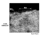
- FIG. 15 is an SCM photograph in which the electric capacity of the surface of the PTC element in which an electrode is provided on a part of the surface of the semiconductor porcelain composition is examined with a scanning capacitance microscope (manufactured by Veeco, model: NanoScope Iva AFM Dimension 3100).
- FIG. 16 is a schematic diagram showing the density of electric capacity of the depletion layer divided into three stages by tracing the crystal grain boundaries in FIG.
- the capacitance C of the depletion layer is proportional to the donor concentration, that is, the square root of the level concentration at the interface between the semiconductor ceramic composition and the electrode, as shown in the following (Equation 2).
- a region having a high level concentration has a large capacitance C and appears dark.
- FIGS. 15 and 16 show the changes in capacitance while changing the voltage applied to the interface between the semiconductor ceramic composition and the electrode. 15 and 16, the higher the density region, the larger the capacitance C.
- a region e having a large capacitance that is, a region having a high level concentration, or a region f having a middle level of capacitance / level concentration appears in the vicinity of the interface where the electrode is formed. It was confirmed that many were formed.
- a region with a low electric capacity that is, a region with a low level concentration appears on the end face where the electrode is not formed or inside the semiconductor composition, and it is confirmed that these regions are regions g with a low concentration even if there is a depletion layer. It was done. Since this level concentration increases as the Bi porosity increases, it is estimated that a depletion layer is formed to such an extent that jump characteristics can be expressed.
- the interface level concentration increases, the temperature coefficient of resistance falls below 5% / ° C, jump characteristics are not exhibited, room temperature resistivity is too large, and resistance values can be measured. There is not.
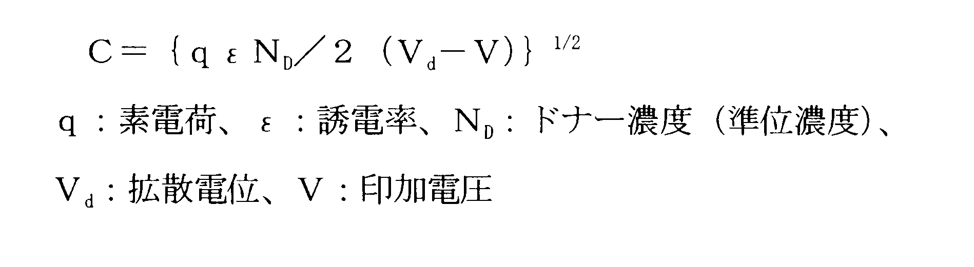
- the width (width of the depletion layer) w of the Schottky barrier at the interface between the metal and the semiconductor ceramic composition is obtained by the following (Equation 3).
- This equation indicates that the width w of the region showing the Schottky barrier is inversely proportional to the electric capacity C.
- the width w e of the region showing the Schottky barrier in the region e showing the large capacitance C is smaller than the width w f of the region f showing the medium capacitance C. This is consistent with the results of FIGS.
- the depletion layer width of the heavily doped region e in the vicinity of the interface (depth) w e is 0.04 ⁇ 0.8 [mu] m
- the depletion layer of the medium density region f width (depth) w f was found to be approximately 2 ⁇ m.
- the room temperature specific resistance ⁇ 25 , the Curie temperature Tsc, and the resistance temperature coefficient ⁇ are influenced by the silver / silver zinc electrode. It can be confirmed from Table 3 that this is the same even when other electrodes are used.
- the PTC element of the present invention was sandwiched and fixed between metal radiating fins 20a1, 20b1, and 20c1 as shown in FIG.
- the electrodes 2a and 2c formed on one surface of the heating element 11 are in thermal and electrical contact with the power supply electrodes 20a and 20c, respectively, and the electrode 2b formed on the other surface is thermally and electrically connected to the power supply electrode 20b. Is closely attached.
- the power supply electrodes 20a, 20b, and 20c are thermally connected to the radiation fins 20a1, 20b1, and 20c1, respectively.
- the insulating layer 2d is provided between the power supply electrode 20a and the power supply electrode 20c, and electrically insulates them. Heat generated in the heating element 11 is transmitted in the order of the electrodes 2a, 2b, 2c, the power supply electrodes 20a, 20b, 20c, and the radiation fins 20a1, 20b1, 20c1, and is mainly released from the radiation fins 20a1, 20b1, 20c1 into the atmosphere. .
- the power supply 30c is connected between the power supply electrode 20a and the power supply electrode 20b, or between the power supply electrode 20c and the power supply electrode 20b, the power consumption is reduced, and both the power supply electrode 20a and the power supply electrode 20c If it connects between the electric power supply electrodes 20b, power consumption will become large. That is, the power consumption can be changed in two stages. In this way, the heating element module 20 can switch the heating capacity according to the load condition of the power source 30c and the desired degree of heating.
- the heating device 30 can be configured by connecting the heating element module 20 capable of switching the heating capacity to the power source 30c.
- the power source 30c may be either direct current / alternating current.
- the power supply electrode 20a and the power supply electrode 20c of the heating element module 20 are connected in parallel to one electrode of the power supply 30c via separate switches 30a and 30b, respectively, and the power supply electrode 20b is the other electrode of the power supply 30c as a common terminal. Connected to.
- the heating capacity can be reduced and the load of the power source 30c can be reduced, and if both are turned on, the heating capacity can be increased.
- the element 2 can be maintained at a constant temperature without providing a special mechanism to the power source 30c. That is, when the element 2 having PTCR characteristics is heated to near the Curie temperature, the resistance value of the element 2 rapidly increases, the current flowing through the element 2 decreases, and the element 2 is not automatically heated any more. Further, when the temperature of the element 2 decreases from around the Curie temperature, a current flows again to the element, and the element 2 is heated. Such a cycle can be repeated to make the temperature of the element 2 and thus the entire heating element module 20 constant. Therefore, a circuit for adjusting the phase and amplitude of the power supply 30c, a temperature detection mechanism, and a comparison mechanism with a target temperature Also, a heating power adjustment circuit and the like are unnecessary.
- the heating device 30 may flow air between the radiation fins 20a1 to 20c1 to warm the air, or connect a metal tube through which a liquid such as water passes between the radiation fins 20a1 to 20c1 to warm the liquid. it can. Also at this time, the element 2 is kept at a constant temperature, so that a safe heating device 30 can be obtained.
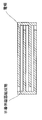
- heating element module 12 according to a modification of the present invention will be described with reference to FIG. In FIG. 18, a part of the heating element module 12 is notched for the sake of explanation.
- the heating element module 12 is a substantially flat rectangular parallelepiped module, and includes an element 3 in which the semiconductor ceramic composition of the example is processed into a substantially rectangular parallelepiped shape, electrodes 3a and 3b provided on the upper and lower surfaces of the element 3, and an element 3 and the insulating coating layer 5 covering the electrodes 3a and 3b, and lead electrodes 4a and 4b connected to the electrodes 3a and 3b and exposed to the outside from the insulating coating layer 5, respectively.
- the heating element module 12 is provided with a plurality of through holes 6 that penetrate the upper and lower surfaces of the heating element module 12 and whose inner peripheral surface is covered with the insulating coating layer 5.
- the heating element module 12 can be manufactured as follows. First, a plurality of holes penetrating in the thickness direction of the element 3 are formed in the element 3 processed from the semiconductor ceramic composition of Example 1. Next, electrodes 3 a and 3 b are formed on both surfaces of the element 3 except for the opening periphery where the holes open on the upper and lower surfaces of the element 3. The electrodes 3a and 3b are formed by printing an ohmic electrode and a surface electrode in the same manner as described above. Further, after providing the external extraction electrodes 4a and 4b, the insulating coating layer 5 is formed by covering the entire element 3 and the electrodes 3a and 3b with an insulating coating agent so that the extraction electrodes 4a and 4b are exposed to the outside. Thus, the heating element module 12 is obtained. In forming the insulating coating layer 5, the through hole 6 is formed by covering the inner peripheral surface of the hole of the element 3 with the insulating coating layer 5.
- the heating element module 12 can heat the fluid by flowing the fluid through the through hole 6. At this time, since the element 3 and the electrodes 3a and 4a through which the current flows are covered with the insulating coating layer 5, the conductive liquid can be heated because it is not in direct contact with the fluid. Therefore, the heating element module 12 is suitable for an application that instantaneously heats a fluid such as salt water having electrical conductivity.
Landscapes
- Engineering & Computer Science (AREA)
- Chemical & Material Sciences (AREA)
- Ceramic Engineering (AREA)
- Materials Engineering (AREA)
- Manufacturing & Machinery (AREA)
- Structural Engineering (AREA)
- Organic Chemistry (AREA)
- Inorganic Chemistry (AREA)
- Physics & Mathematics (AREA)
- Microelectronics & Electronic Packaging (AREA)
- Thermal Sciences (AREA)
- Electromagnetism (AREA)
- Thermistors And Varistors (AREA)
- Compositions Of Oxide Ceramics (AREA)
Abstract
Description
そこで本発明は、Pbフリーの半導体磁器組成物を用いて薄型で、且つ耐電圧性に優れたPTC素子を提供することを目的とする。
(1) 少なくとも2つの金属電極と、前記電極の間に配置されたBaTiO3系半導体磁器組成物とを有するPTC素子であって、
前記半導体磁器組成物は、BaTiO3系のBaの一部がBi-Naと半導体化元素で置換され、少なくともBiサイトに空孔が形成されて、その結晶に酸素欠陥が形成されていることを特徴とするPTC素子。
(2) 前記Biの空孔率がBiサイトに対して5%より大きく、75%以下であることを特徴とする(1)のPTC素子。
(3) 前記酸素欠陥がOサイトに対して10ppm以下であることを特徴とする(1)または(2)のPTC素子。
(4) 前記BiサイトのほかにNaサイトにも空孔が形成されており、当該Naの空孔率がNaサイトに対して0%より大きく、60%以下であることを特徴とする(1)~(3)のいずれかのPTC素子。
(5) 前記BiサイトのほかにBaサイトにも空孔が形成されており、当該Baの空孔率がBaサイトに対して0%より大きく、4%以下であることを特徴とする(1)~(4)のいずれかのPTC素子。
(6) 少なくとも2つの金属電極と、前記電極の間に配置されたBaTiO3系半導体磁器組成物とを有するPTC素子であって、
前記半導体磁器組成物は、BaTiO3系のBaの一部がBi-Naと半導体化元素で置換され、少なくともBiサイトに空孔が形成されて、その結晶に酸素欠陥が形成されたものであり、
前記金属電極と半導体磁器組成物との間の界面近傍に空乏層が存在することを特徴とするPTC素子。
(7) 前記金属電極と半導体磁器組成物との間の界面から2μm以内に空乏層があることを特徴とする(6)のPTC素子。また、前記空乏層の幅は0.04μm~0.8μmであってもよい。
(8) 前記電極と、前記半導体磁器組成物とを積層させてなることを特徴とする(1)~(7)のいずれかのPTC素子。
(9) (1)~(8)のいずれかのPTC素子と、前記PTC素子に設けられた電力供給電極とを備えることを特徴とする発熱体モジュール。
<実施例>
作製したPTC素子を14℃から256℃まで加熱し、両電極間の抵抗値を4端子法で測定し、抵抗値の温度変化を測定した。その結果を図1に示す。
そこで、本発明の発明者は、電極を構成する金属の種類を変えた時にジャンプ特性も変化すれば上記モデルの妥当性が証明されると考え、金属の種類を変えて上記の抵抗値R0(T)を調べたものが図6~図10である。図6~図10は、図1,3で測定したPTC素子のうち、10mm×10mm×1.00mmのPTC素子について、各温度での厚みが0の時の抵抗値R0(T)を算出して、温度と厚み0の抵抗値R0(T)の関係を示している。
図7で測定したPTC素子は、カバー電極としての銀電極とオーミック電極としてのニッケル電極をスパッタリングで形成し、その後酸素中で300℃、3時間の熱処理を施したものである。
図8で測定したPTC素子は、カバー電極としての銀電極とオーミック電極としてのニッケル電極とをスパッタリングで形成し、熱処理を行わなかったものである。
図9で測定したPTC素子は、カバー電極としてのチタン電極とオーミック電極としての銅電極とをスパッタリングで形成し、大気中で300℃、5時間の熱処理を施したものである。
図10で測定したPTC素子は、カバー電極としてのニッケル電極とオーミック電極としてのチタン電極とをスパッタリングで形成し、大気中で300℃、5時間の熱処理を施したものである。
さらに、半導体磁器組成物と金属電極との界面で抵抗成分が発生していることから、中間層電極を設けて界面を増やした場合の室温比抵抗ρ25、キュリー温度Tsc、抵抗温度係数αについて測定した。なお、半導体磁器組成物の抵抗測定値から材料中の抵抗値(全体の抵抗値)と、電極と材料の界面での抵抗値(厚み0の時の抵抗値R0(T))とを分離し、界面の抵抗値が室温における界面の抵抗値の2倍となったときの温度を便宜的にキュリー温度Tscとした。
α=(lnR2―lnR1)×100/(T2-T1)
T1はキュリー温度Tscを超えて比抵抗が室温比抵抗ρ25の2倍になる温度、T2は最大比抵抗を示す温度、R1,R2はそれぞれ温度T1,T2の時の抵抗値である。この抵抗温度係数αは、ジャンプの前後でどれくらい抵抗値が増加したかを示す指標であり、数値が大きいほどジャンプ特性に優れていることを示す。

図12は、半導体磁器組成物の両端に銀のカバー電極、ニッケルの中間電極、クロムのオーミック電極からなる電極をスパッタリングで形成し、熱処理を行わなかった試験片の温度―厚み0の抵抗値R0(T)の測定結果である。
図13は、半導体磁器組成物の両端に銀のカバー電極、ニッケルの中間電極、クロムのオーミック電極からなる電極をスパッタリングで形成し、大気中で300℃、5時間の熱処理を施した試験片の温度―厚み0の抵抗値R0(T)の測定結果である。
図14は、半導体磁器組成物の両端に銀のカバー電極、ニッケルの中間電極、クロムのオーミック電極からなる電極をスパッタリングで形成し、酸素中で300℃、5時間の熱処理を施した試験片の温度―厚み0の抵抗値R0(T)の測定結果である。
次に、上記のジャンプ特性に影響を及ぼす半導体磁器組成物中の原子空孔率について考察した。上記実施例の組成[(Bi-Na)x(Ba1-yLay)1-x]TiO3についてBi,Ba,Na,Oの空孔率を分析した。これは、理論上Ti:1に対し、BiやNaは0.08×0.5が含まれているべきところ、実際の半導体磁器組成物を分析した結果、Bi,Ba,Na,Oの値があるべき数値より少なくなっているので、Bi,Ba,Na,Oサイトに欠陥が生じていると推定されたからである。そこで、これらの欠陥の度合いが、室温比抵抗ρ25、キュリー温度Tsc、抵抗温度係数αに対して影響を及ぼすとの着想を得て分析した。

Biの空孔率が範囲であれば、空乏層を有する(ショットキー障壁を有する)界面を構成し易い。したがって、Bi空孔率が80%を超えないように、原料粉末の調整段階では、Bi0.5-γNa0.5-η)TiO3のうちγが0.4を超えないようにBi2O3の投入量を調整することが好ましい。
なお、γが、0.4を超えて、極めて大きくなる場合は、正常な正方晶相にBiが欠如した異相が極めて多く形成されてしまうため、できるだけ仮焼きや焼結段階でBiを揮散させることが好ましい。これによって異相生成を最小限に抑え、Bi欠陥を正方晶内に形成することができる。
同様の理由で、後述するNaについても同様にηはできるだけ小さいことが好ましい。なお、Baは飽和蒸気圧が低いので仮焼きや焼結段階で揮散させることができないので、原料粉の調整段階で水中にBaを溶出させるなどして調整する。
すなわち、Ba空孔率が4%、Na空孔率が60%を超えるよう調整された場合、ジャンプ特性は発現するものの、半導体磁器組成物中のBaやNaの空孔比率が多くなりすぎて規則的な結晶構造が形成されず、異相が形成されてしまうので好ましくない。また、金属と半導体磁器組成物との界面で上述のジャンプ特性が発現し、このジャンプ特性がBi、Oの空孔率に影響されることを考慮すると、金属と半導体磁器組成物との界面に空乏層が存在すると考えられる。


<発熱体モジュール>
Claims (9)
- 少なくとも2つの金属電極と、前記電極の間に配置されたBaTiO3系半導体磁器組成物とを有するPTC素子であって、
前記半導体磁器組成物は、BaTiO3系のBaの一部がBi-Naと半導体化元素で置換され、少なくともBiサイトに空孔が形成されて、その結晶に酸素欠陥が形成されたものであることを特徴とするPTC素子。 - 前記Biの空孔率がBiサイトに対して5%より大きく、75%以下であることを特徴とする請求項1に記載のPTC素子。
- 前記酸素欠陥がOサイトに対して10ppm以下であることを特徴とする請求項1または2に記載のPTC素子。
- 前記BiサイトのほかにNaサイトにも空孔が形成されており、当該Naの空孔率がNaサイトに対して0%より大きく、60%以下であることを特徴とする請求項1~3の何れかに記載のPTC素子。
- 前記BiサイトのほかにBaサイトにも空孔が形成されており、当該Baの空孔率がBaサイトに対して0%より大きく、4%以下であることを特徴とする請求項1~4の何れかに記載のPTC素子。
- 少なくとも2つの金属電極と、前記電極の間に配置されたBaTiO3系半導体磁器組成物とを有するPTC素子であって、
前記半導体磁器組成物は、BaTiO3系のBaの一部がBi-Naと半導体化元素で置換され、少なくともBiサイトに空孔が形成されて、その結晶に酸素欠陥が形成されたものであり、
前記金属電極と半導体磁器組成物との間の界面近傍に空乏層が存在することを特徴とするPTC素子。 - 前記金属電極と半導体磁器組成物との間の界面から2μm以内に空乏層があることを特徴とする請求項6に記載のPTC素子。
- 前記電極と、前記半導体磁器組成物とを積層させてなることを特徴とする請求項1~7の何れか1項に記載のPTC素子。
- 請求項1~8の何れか1項に記載のPTC素子と、前記PTC素子に設けられた電力供給電極とを備えることを特徴とする発熱体モジュール。
Priority Applications (4)
| Application Number | Priority Date | Filing Date | Title |
|---|---|---|---|
| CN201180017538.8A CN102822911B (zh) | 2010-04-08 | 2011-04-06 | Ptc元件和加热元件模块 |
| EP11765940.9A EP2557575A4 (en) | 2010-04-08 | 2011-04-06 | PTC ELEMENT AND HEAT ELEMENT MODULE |
| US13/639,804 US8686827B2 (en) | 2010-04-08 | 2011-04-06 | PTC element and heating-element module |
| JP2012509682A JP5803906B2 (ja) | 2010-04-08 | 2011-04-06 | Ptc素子と発熱体モジュール |
Applications Claiming Priority (2)
| Application Number | Priority Date | Filing Date | Title |
|---|---|---|---|
| JP2010-089758 | 2010-04-08 | ||
| JP2010089758 | 2010-04-08 |
Publications (1)
| Publication Number | Publication Date |
|---|---|
| WO2011126040A1 true WO2011126040A1 (ja) | 2011-10-13 |
Family
ID=44762974
Family Applications (1)
| Application Number | Title | Priority Date | Filing Date |
|---|---|---|---|
| PCT/JP2011/058681 Ceased WO2011126040A1 (ja) | 2010-04-08 | 2011-04-06 | Ptc素子と発熱体モジュール |
Country Status (6)
| Country | Link |
|---|---|
| US (1) | US8686827B2 (ja) |
| EP (1) | EP2557575A4 (ja) |
| JP (1) | JP5803906B2 (ja) |
| CN (1) | CN102822911B (ja) |
| TW (1) | TWI470653B (ja) |
| WO (1) | WO2011126040A1 (ja) |
Cited By (2)
| Publication number | Priority date | Publication date | Assignee | Title |
|---|---|---|---|---|
| WO2013051486A1 (ja) | 2011-10-03 | 2013-04-11 | 日立金属株式会社 | 半導体磁器組成物、ptc素子、および発熱モジュール |
| JP2017005020A (ja) * | 2015-06-05 | 2017-01-05 | 株式会社村田製作所 | 積層セラミックコンデンサの製造方法 |
Families Citing this family (4)
| Publication number | Priority date | Publication date | Assignee | Title |
|---|---|---|---|---|
| KR102116675B1 (ko) * | 2015-12-04 | 2020-05-29 | 가부시키가이샤 무라타 세이사쿠쇼 | 유전체 자기 조성물, 적층 세라믹 콘덴서 및 적층 세라믹 콘덴서의 제조 방법 |
| WO2017104539A1 (ja) * | 2015-12-18 | 2017-06-22 | 株式会社村田製作所 | 誘電体磁器組成物、誘電体磁器組成物の製造方法、及び積層型セラミック電子部品 |
| CN107721412A (zh) * | 2017-11-13 | 2018-02-23 | 陕西科技大学 | 一种nbt基半导体陶瓷及其制备方法 |
| CN113475755B (zh) * | 2021-08-06 | 2024-07-09 | 广东省奇思智能制造有限公司 | 发热体及其制备方法和雾化器、雾化装置 |
Citations (6)
| Publication number | Priority date | Publication date | Assignee | Title |
|---|---|---|---|---|
| JPS56169301A (en) * | 1980-06-02 | 1981-12-26 | Tohoku Metal Ind Ltd | Method of producing barium titanate semiconductor porcelain |
| JP2006179692A (ja) * | 2004-12-22 | 2006-07-06 | Komatsu Electronics Inc | サーミスタの製造方法 |
| WO2006118274A1 (ja) * | 2005-04-28 | 2006-11-09 | Hitachi Metals, Ltd. | 半導体磁器組成物とその製造方法 |
| JP2008063188A (ja) * | 2006-09-07 | 2008-03-21 | Furukawa Co Ltd | Ptcサーミスタ用配合材料およびptcサーミスタ用半導体磁器組成物 |
| WO2008038538A1 (fr) * | 2006-09-28 | 2008-04-03 | Murata Manufacturing Co., Ltd. | Composition de porcelaine semiconductrice de titanate de baryum et dispositif ptc utilisant celle-ci |
| JP2010089758A (ja) | 2008-10-10 | 2010-04-22 | Autonetworks Technologies Ltd | 車両用電源装置 |
Family Cites Families (8)
| Publication number | Priority date | Publication date | Assignee | Title |
|---|---|---|---|---|
| JPS4827556A (ja) | 1971-08-13 | 1973-04-11 | ||
| TW369514B (en) * | 1994-01-13 | 1999-09-11 | Tam Ceramics Inc | A method of sintering Pb(Mg1/3Nb2/3)O3 or the oxide precursors thereof without using lead oxide |
| JP3498211B2 (ja) * | 1999-12-10 | 2004-02-16 | 株式会社村田製作所 | 積層型半導体セラミック電子部品 |
| JP4827556B2 (ja) | 2005-03-18 | 2011-11-30 | キヤノン株式会社 | 積層型半導体パッケージ |
| US8067325B2 (en) * | 2006-02-27 | 2011-11-29 | Hitachi Metals, Ltd. | Semiconductor ceramic composition |
| US20090105064A1 (en) * | 2006-10-27 | 2009-04-23 | Takeshi Shimada | Semiconductor ceramic composition and method for producing the same |
| JP5251119B2 (ja) * | 2007-12-26 | 2013-07-31 | 日立金属株式会社 | 半導体磁器組成物 |
| JP5590494B2 (ja) * | 2008-03-27 | 2014-09-17 | 日立金属株式会社 | 半導体磁器組成物−電極接合体の製造方法 |
-
2011
- 2011-04-06 EP EP11765940.9A patent/EP2557575A4/en not_active Withdrawn
- 2011-04-06 CN CN201180017538.8A patent/CN102822911B/zh not_active Expired - Fee Related
- 2011-04-06 WO PCT/JP2011/058681 patent/WO2011126040A1/ja not_active Ceased
- 2011-04-06 US US13/639,804 patent/US8686827B2/en not_active Expired - Fee Related
- 2011-04-06 JP JP2012509682A patent/JP5803906B2/ja not_active Expired - Fee Related
- 2011-04-08 TW TW100112183A patent/TWI470653B/zh not_active IP Right Cessation
Patent Citations (6)
| Publication number | Priority date | Publication date | Assignee | Title |
|---|---|---|---|---|
| JPS56169301A (en) * | 1980-06-02 | 1981-12-26 | Tohoku Metal Ind Ltd | Method of producing barium titanate semiconductor porcelain |
| JP2006179692A (ja) * | 2004-12-22 | 2006-07-06 | Komatsu Electronics Inc | サーミスタの製造方法 |
| WO2006118274A1 (ja) * | 2005-04-28 | 2006-11-09 | Hitachi Metals, Ltd. | 半導体磁器組成物とその製造方法 |
| JP2008063188A (ja) * | 2006-09-07 | 2008-03-21 | Furukawa Co Ltd | Ptcサーミスタ用配合材料およびptcサーミスタ用半導体磁器組成物 |
| WO2008038538A1 (fr) * | 2006-09-28 | 2008-04-03 | Murata Manufacturing Co., Ltd. | Composition de porcelaine semiconductrice de titanate de baryum et dispositif ptc utilisant celle-ci |
| JP2010089758A (ja) | 2008-10-10 | 2010-04-22 | Autonetworks Technologies Ltd | 車両用電源装置 |
Non-Patent Citations (1)
| Title |
|---|
| See also references of EP2557575A4 |
Cited By (2)
| Publication number | Priority date | Publication date | Assignee | Title |
|---|---|---|---|---|
| WO2013051486A1 (ja) | 2011-10-03 | 2013-04-11 | 日立金属株式会社 | 半導体磁器組成物、ptc素子、および発熱モジュール |
| JP2017005020A (ja) * | 2015-06-05 | 2017-01-05 | 株式会社村田製作所 | 積層セラミックコンデンサの製造方法 |
Also Published As
| Publication number | Publication date |
|---|---|
| JPWO2011126040A1 (ja) | 2013-07-11 |
| US20130037904A1 (en) | 2013-02-14 |
| EP2557575A1 (en) | 2013-02-13 |
| TWI470653B (zh) | 2015-01-21 |
| US8686827B2 (en) | 2014-04-01 |
| EP2557575A4 (en) | 2013-12-11 |
| JP5803906B2 (ja) | 2015-11-04 |
| CN102822911A (zh) | 2012-12-12 |
| TW201212050A (en) | 2012-03-16 |
| CN102822911B (zh) | 2015-11-25 |
Similar Documents
| Publication | Publication Date | Title |
|---|---|---|
| JP5757239B2 (ja) | 半導体磁器組成物およびその製造方法、ptc素子および発熱モジュール | |
| JP5803906B2 (ja) | Ptc素子と発熱体モジュール | |
| CN103748056B (zh) | 半导体陶瓷组合物、正温度系数元件和发热模块 | |
| WO2013157650A1 (ja) | 半導体磁器組成物の製造方法 | |
| JP2005255493A (ja) | 半導体磁器組成物 | |
| KR20170016805A (ko) | 반도체 자기 조성물 및 ptc 서미스터 | |
| KR20170094085A (ko) | 반도체 자기 조성물 및 ptc 서미스터 | |
| Li et al. | Sb–doped ZnO ceramics: NTC thermistors with high temperature sensitivity and electrical stability | |
| JP5590494B2 (ja) | 半導体磁器組成物−電極接合体の製造方法 | |
| Xiang et al. | Positive temperature coefficient of resistivity effect of semiconducting BaTiO3–(Bi1/2Na1/2) TiO3 ceramics prepared by a wet-chemistry route | |
| JP5765611B2 (ja) | Ptc素子および発熱モジュール | |
| JP5626204B2 (ja) | 半導体磁器組成物、発熱体及び発熱モジュール | |
| JP2012004496A (ja) | Ptc素子および発熱モジュール | |
| JP5263668B2 (ja) | 半導体磁器組成物 | |
| JP2012036032A (ja) | 半導体磁器組成物、その製造方法、ptc素子及び発熱モジュール | |
| JP2012046372A (ja) | Ptc素子および発熱モジュール | |
| JP2012001416A (ja) | Ptc素子および発熱モジュール | |
| JP2012224537A (ja) | Ptc素子用焼結体、その製造方法、ptc素子、及び発熱モジュール | |
| JP5737634B2 (ja) | 半導体磁器組成物の製造方法 | |
| CN105359227A (zh) | Ptc元件和发热模块 | |
| Wei et al. | Enhanced Ptcr Effect of (Ba, Pb) Tio3-Based Ceramics by Appropriate Al2o3 Addition |
Legal Events
| Date | Code | Title | Description |
|---|---|---|---|
| WWE | Wipo information: entry into national phase |
Ref document number: 201180017538.8 Country of ref document: CN |
|
| 121 | Ep: the epo has been informed by wipo that ep was designated in this application |
Ref document number: 11765940 Country of ref document: EP Kind code of ref document: A1 |
|
| WWE | Wipo information: entry into national phase |
Ref document number: 2012509682 Country of ref document: JP |
|
| WWE | Wipo information: entry into national phase |
Ref document number: 13639804 Country of ref document: US |
|
| NENP | Non-entry into the national phase |
Ref country code: DE |
|
| WWE | Wipo information: entry into national phase |
Ref document number: 2011765940 Country of ref document: EP |