WO2011136312A1 - 振動発電デバイスおよびその製造方法 - Google Patents
振動発電デバイスおよびその製造方法 Download PDFInfo
- Publication number
- WO2011136312A1 WO2011136312A1 PCT/JP2011/060346 JP2011060346W WO2011136312A1 WO 2011136312 A1 WO2011136312 A1 WO 2011136312A1 JP 2011060346 W JP2011060346 W JP 2011060346W WO 2011136312 A1 WO2011136312 A1 WO 2011136312A1
- Authority
- WO
- WIPO (PCT)
- Prior art keywords
- power generation
- generation device
- vibration
- weight
- silicon substrate
- Prior art date
- Legal status (The legal status is an assumption and is not a legal conclusion. Google has not performed a legal analysis and makes no representation as to the accuracy of the status listed.)
- Ceased
Links
Images



Classifications
-
- H—ELECTRICITY
- H10—SEMICONDUCTOR DEVICES; ELECTRIC SOLID-STATE DEVICES NOT OTHERWISE PROVIDED FOR
- H10N—ELECTRIC SOLID-STATE DEVICES NOT OTHERWISE PROVIDED FOR
- H10N30/00—Piezoelectric or electrostrictive devices
- H10N30/30—Piezoelectric or electrostrictive devices with mechanical input and electrical output, e.g. functioning as generators or sensors
- H10N30/304—Beam type
- H10N30/306—Cantilevers
-
- H—ELECTRICITY
- H02—GENERATION; CONVERSION OR DISTRIBUTION OF ELECTRIC POWER
- H02N—ELECTRIC MACHINES NOT OTHERWISE PROVIDED FOR
- H02N2/00—Electric machines in general using piezoelectric effect, electrostriction or magnetostriction
Definitions
- the present invention relates to a vibration power generation device configured to convert vibration energy into electric energy using MEMS (micro-electromechanical systems) technology and a method for manufacturing the same.
- MEMS micro-electromechanical systems
- the power generation device shown in the above-mentioned document 1 includes a main substrate 4, a first cover substrate 5, and a second cover substrate 6, as shown in FIG.
- the main substrate 4 includes a frame portion 1 and a weight portion 3 that is disposed inside the frame portion 1 and is swingably supported via a flexible bending portion 2, and is formed using an element forming substrate.
- the first cover substrate 5 is formed using the first cover forming substrate, and the frame portion 1 is fixed to one surface side of the main substrate 4.
- the second cover substrate 6 is formed using a second cover forming substrate, and the frame portion 1 is fixed to the other surface side of the main substrate 4.
- a power generation unit 7 that generates an AC voltage in response to vibration of the weight unit 3 is formed in the bending unit 2 of the main substrate 4.
- the power generation unit 7 has a laminated structure of a lower electrode 8, a piezoelectric layer 9, and an upper electrode 10.
- the density of silicon that becomes the weight portion 3 is relatively smaller than that of the metal material, and the silicon that becomes the flexure portion 2 has a Young's modulus greater than that of the metal material. There was a problem that the weight portion 3 did not vibrate sufficiently and the output was reduced.
- the elastic film is formed to extend to the weight portion.
- the frame portion and the weight portion are formed using a silicon substrate on which an etching stop layer is formed, and the bending portion is formed by etching the silicon substrate until reaching the etching stop layer. It is preferable to form.
- FIG. 3 is a schematic plan view of a modification example of an elastic film part in the vibration power generation device showing one embodiment and a schematic cross-sectional view taken along the line AA ′ of FIG. 2 of a modification example of the silicon substrate part.
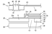
- 1 is a schematic exploded cross-sectional view of a vibration power generation device showing an embodiment of the present invention.
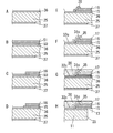
- FIG. 3 is a main process cross-sectional view taken along the line AA ′ of FIG. 2 for explaining a method for manufacturing a silicon substrate portion in the vibration power generation device showing one embodiment of the present invention. It is a schematic sectional drawing of the vibration electric power generation device which shows a prior art example.
- This vibration power generation device includes at least a frame part 11, a weight part 12, a bending part 13, and a power generation part 18.
- the weight portion 12 is provided inside the frame portion 11.
- the bending part 13 connects between the frame part 11 and the weight part 12 and is formed to bend when the weight part 12 is displaced.
- the power generation unit 18 is disposed at least in the bending unit 13 and is configured to generate an AC voltage according to the vibration of the weight unit 12.
- the frame part 11 and the weight part 12 are formed using a silicon substrate 25.
- An elastic film 20 made of a resin material is formed on the surface of the power generation unit 18.
- the bending portion 13 is made of an elastic film 20 formed using a resin material having a Young's modulus smaller than that of silicon constituting the frame portion 11 and the weight portion 12.
- the elastic film 20 is formed to extend to the weight portion 12.
- this vibration power generation device has a first cover substrate 29 fixed to the frame portion 11 on the first surface of a silicon substrate 25.
- the vibration power generation device includes a second cover substrate 30 fixed to the frame portion 11 on the second surface opposite to the first surface of the silicon substrate 25.
- the first cover substrate 29 and the second cover substrate 30 are formed using silicon, glass, or the like.
- the vibration power generation device is configured using the silicon substrate 25, the first cover substrate 29, and the second cover substrate 30.
- the outer shape of the frame portion 11 in plan view is a rectangular shape. Further, the outer shape in plan view of the weight portion 12 and the bending portion 13 formed inside the frame portion 11 is also rectangular like the outer shape of the frame portion 11. Further, the outer shape of the power generation unit 18 arranged in the bending portion 13 in a plan view is a rectangular shape along the outer shape of the bending portion 13.
- the weight portion 12 includes first and second ends, and has a free end and a supported end at the first and second ends, respectively. The supported end is supported by a part of the frame part 11 as a support part via the bending part 13. In the example of FIG.
- the frame portion 11 is a rectangular frame having a rectangular hole
- the weight portion 12 is a rectangular plate disposed in the frame portion 11
- the first and second ends are weights. It corresponds to both ends in the longitudinal direction of the portion 12.
- the elastic film 20 is formed at least between the edge of the supported end of the weight part 12 and the edge of the support part of the frame part 11.
- the elastic film 20 may be formed of a resin material so as to cover the entire first surface side of the silicon substrate 25.
- the elastic film 20 is provided with a through hole 23 at a position corresponding to the lower electrode pad 32a and the upper electrode pad 32c, and a metal film is formed in the through hole 23. Is deposited.
- PMMA polymethyl methacrylate resin
- polyimide polyimide
- the elastic film 20 only needs to cover at least the power generation unit 18. In such a case, if the lower electrode pad 32a and the upper electrode pad 32c are exposed on the surface, it is not necessary to provide the through hole 23.
- the shape of the through hole 23 in a plan view is not limited to this as long as wiring can be installed, such as a substantially square shape or a substantially circular shape.
- an insulating portion 35 for preventing a short circuit between the connection wiring 31 c electrically connected to the upper electrode 17 and the lower electrode 15 is provided in each of the frame portions in the lower electrode 15 and the piezoelectric layer 16. It is formed so as to cover the end portion on the 11 side. Further, when the insulating portion 35 is provided, the insulating portion 35 is configured by a silicon oxide film, but is not limited to a silicon oxide film, and may be configured by a silicon nitride film. A seed layer (not shown) made of an MgO layer is formed between the silicon substrate 25 and the lower electrode 15. Silicon oxide films 36 and 37 are formed on the first surface side and the second surface side of the silicon substrate 25, respectively.
- the substrate material constituting the silicon substrate 25 is silicon
- the silicon oxide film 36 on the first surface of the silicon substrate becomes an etching stop layer.
- the elastic film 20 has through-holes 23 at positions corresponding to the AC voltage taken out from the lower electrode pad 32a and the upper electrode pad 32c.
- the first cover substrate 29 has first and second surfaces, and the second surface of the first cover substrate 29 is bonded to the first surface side of the silicon substrate 25.
- a displacement space of the movable portion composed of the weight portion 12 and the bending portion 13 is formed in a part of the second surface side on the silicon substrate 25 side, and the displacement space is defined as a first recess 38.
- Output electrodes 40 and 40 for supplying the AC voltage generated by the power generation unit 18 to the outside are formed on the first surface side of the first cover substrate 29.
- the output electrodes 40, 40 are respectively connected electrodes 41, 41 formed on the second surface side of the first cover substrate 29 and through-hole wirings penetrating in the thickness direction of the first cover substrate 29. They are electrically connected via 42 and 42.
- the connecting electrodes 41 and 41 of the first cover substrate 29 are joined and electrically connected to the lower electrode pad 32a and the upper electrode pad 32c of the silicon substrate 25, respectively.
- the output electrodes 40 and 40 and the connection electrodes 41 and 41 are each composed of a laminated film of a Ti film and an Au film, but these materials and layer structures are not particularly limited.
- Cu is adopted as the material of each through-hole wiring 42, 42, it is not limited to this, and for example, Ni, Al, or the like may be adopted.
- the second cover substrate 30 has first and second surfaces, and the first surface of the second cover substrate 30 is bonded to the second surface side of the silicon substrate 25. On the first surface side of the second cover substrate 30, a displacement space of the movable portion composed of the weight portion 12 and the bending portion 13 is formed, and the displacement space is a second recess 39.
- the second cover substrate 30 may be an insulating substrate such as a glass substrate.
- the silicon substrate 25 provided with the elastic film 20 and the first cover substrate 29 are bonded together with an adhesive or the like.
- the silicon substrate 25 and the second cover substrate 30 are bonded by a room temperature bonding method, but not limited to the room temperature bonding method, for example, by an anodic bonding method or a resin bonding method using an epoxy resin or the like. You may join.
- the vibration power generation device of the present embodiment is formed by using a MEMS device manufacturing technique or the like.
- the piezoelectric layer 16 is stressed by vibration of the flexure 13. As a result, a bias of electric charge occurs between the lower electrode 15 and the upper electrode 17, and an AC voltage is generated in the power generation unit 18.
- the relative dielectric constant of the piezoelectric material used for the piezoelectric layer 16 of the vibration power generation device is ⁇
- the piezoelectric constant is e
- the power generation index is P
- the relationship P ⁇ e 2 / ⁇ is established, and the power generation index P is large.
- the power generation efficiency increases.
- PZT which is a typical piezoelectric material used for vibration power generation devices, has a large piezoelectric constant e that can be squared to the power generation index P from the general values of the piezoelectric constant e and relative permittivity ⁇ of each of PZT and AlN.
- the power generation index P can be increased.
- the vibration power generation device employs PZT, which is a kind of lead-based piezoelectric material, as the piezoelectric material of the piezoelectric layer 16, but the lead-based piezoelectric material is not limited to PZT, for example, PZT-PMN (: PZT to which Pb (Mn, Nb) O 3 ) or other impurities are added may be employed.
- PZT-PMN PZT to which Pb (Mn, Nb) O 3
- the piezoelectric material of the piezoelectric layer 16 is not limited to the lead-based piezoelectric material, and other piezoelectric materials may be adopted.
- FIGS. 5A to 5H show portions corresponding to the AA ′ cross section of FIG.
- an insulating film forming step is performed in which silicon oxide films 36 and 37 are respectively formed on the first surface side and the second surface side of the silicon substrate 25 formed using silicon by a thermal oxidation method or the like. Get the structure. Specifically, the (first) silicon oxide film 36 is formed on the entire first surface of the silicon substrate 25, while the (second) silicon oxide film 37 is formed on the first surface of the silicon substrate 25 excluding the formation region of the bending portion 13. 2 formed on the surface.
- a piezoelectric film 51 (for example, a PZT film) that forms the basis of the piezoelectric layer 16 made of a piezoelectric material (for example, PZT) is formed on the entire surface of the metal layer 50 by a sputtering method, a CVD method, a sol-gel method, or the like.
- the structure shown in FIG. 5B is obtained by performing the film forming process.
- the metal layer 50 is not limited to the Pt layer, and may be, for example, an Al layer or an Al—Si layer, or a Pt layer and a Ti layer for improving adhesion that is interposed between the Pt layer and the seed layer. May be.
- the material of the adhesion layer is not limited to Ti, but may be Cr, Nb, Zr, TiN, TaN, or the like.
- the piezoelectric film 51 is patterned using photolithography technology and etching technology, and the piezoelectric film patterning step for forming the piezoelectric layer 16 made of a part of the piezoelectric film 51 is performed.
- the structure shown in 5C is obtained.
- connection wiring forming process for forming the connection wiring 31a and a lower electrode pad forming process for forming the lower electrode pad 32a may be provided separately.
- etching of the metal layer 50 for example, an RIE method or an ion milling method may be employed.
- the insulating part forming process is performed.
- the structure shown in 5E is obtained.
- an insulating layer is formed on the entire surface of the first surface side of the substrate 25 by the CVD method and then patterned using the photolithography technique and the etching technique, but the lift-off method is used.
- the insulating portion 35 may be formed.
- the upper electrode 17 is formed simultaneously with the upper electrode forming process in which the upper electrode 17 is formed using a thin film forming technique such as EB vapor deposition, sputtering, or CVD, photolithography, or etching.
- 5C is obtained by performing a wiring formation process in which 31c and upper electrode pad 32c are formed using thin film formation technology such as EB vapor deposition, sputtering, and CVD, photolithography, and etching. .
- the connection wiring 31c and the upper electrode pad 32c are formed together with the upper electrode 17, but not limited thereto, the upper electrode forming process and the wiring forming process May be performed separately.
- a connection wiring formation process for forming the connection wiring 31c and an upper electrode pad formation process for forming the upper electrode pad 32c may be provided separately.
- Etching of the upper electrode 17 is preferably dry etching such as RIE. However, wet etching may be used.
- the Au film may be wet-etched with a potassium iodide aqueous solution, and the Ti film may be wet-etched with hydrogen peroxide water.
- the upper electrode 17 is made of Pt, Al, Al—Si, or the like.
- a substrate processing step for forming the frame portion 11, the weight portion 12, and the bent portion 13 using a photolithography technique, an etching technique, and the like is performed, whereby the structure shown in FIG. Get.
- the substrate processing step portions other than the frame portion 11 and the weight portion 12 are removed by etching until the silicon substrate 25 reaches the silicon oxide film 36 from the second surface side using photolithography technology and etching technology.
- a back surface groove forming step for forming a back surface groove is performed.
- the silicon oxide film 36 is etched to communicate with each other, thereby forming the frame portion 11, the weight portion 12, and the bending portion 13.
- the silicon oxide film 37 is also removed by etching. By performing this etching step, the power generation device having the structure shown in FIG. 5H is obtained.
- the silicon substrate 25 is etched using an inductively coupled plasma (ICP) type etching apparatus capable of vertical deepening in the back surface groove forming step of the substrate processing step, the silicon oxide film 36 is formed.
- the angle formed between the back surface and the inner surface of the frame portion 11 can be approximately 90 degrees.
- the back surface groove forming step of the substrate processing step is not limited to dry etching using an ICP type dry etching apparatus, as long as etching with high anisotropy is possible, and other dry etching apparatuses may be used. .
- wet etching crystal anisotropic etching
- an alkaline solution such as a TMAH aqueous solution or a KOH aqueous solution may be used.
- the power generation device of the present embodiment is divided into individual power generation devices by performing a dicing process after the substrate processing process is completed at the wafer level.
- a joining process is performed.
- the process may be performed at the wafer level until the cover joining process is completed, and then the dicing process may be performed to divide into individual vibration power generation devices.
- the cover substrates 29 and 30 may be formed by appropriately applying known processes such as a photolithography process, an etching process, a thin film forming process, and a plating process.
- the piezoelectric layer 16 is formed on the lower electrode 15, but a buffer layer (not shown) serving as a base when the piezoelectric layer 16 is formed between the lower electrode 15 and the piezoelectric layer 16.
- the crystallinity of the piezoelectric layer 16 may be further improved.
- SrRuO 3 , (Pb, Ra) TiO 3 , PbTiO 3, or the like, which is a kind of conductive oxide material, may be employed.
- the vibration power generation device may be an arrayed vibration power generation device arranged in a two-dimensional array, for example.
- the elastic film 20 is formed to extend to the weight portion 12. From this, it is possible to obtain a larger output by increasing the mass of the weight portion 12 while suppressing breakage of the bent portion 13 due to vibration of the weight portion 12.
Landscapes
- General Electrical Machinery Utilizing Piezoelectricity, Electrostriction Or Magnetostriction (AREA)
- Micromachines (AREA)
Abstract
Description
15と圧電層16との間に、圧電層16の成膜時の下地となるバッファ層(図示せず)を介在させることで、圧電層16の結晶性を更に向上させてもよい。バッファ層の材料としては、導電性酸化物材料の一種であるSrRuO 3、(Pb,Ra)TiO 3、PbTiO 3などを採用すればよい。
Claims (4)
- フレーム部と、前記フレーム部の内側に設けられた錘部と、前記フレーム部と前記錘部との間をつなぎ前記錘部が変位することで撓む撓み部と、少なくとも前記撓み部に配置され前記錘部の振動に応じて交流電圧を発生するように構成される発電部と、を備えた振動発電デバイスであって、
前記フレーム部および前記錘部は、シリコン基板を用いて形成され、
前記発電部の表面には、樹脂材料で形成された弾性膜を備え、
前記撓み部は、前記フレーム部かつ前記錘部を構成するシリコンよりもヤング率が小さな前記樹脂材料を用いて形成した前記弾性膜でなることを特徴とする振動発電デバイス。 - 前記撓み部は、前記弾性膜、および前記シリコン基板に対するエッチングストップ層のうち、少なくとも前記弾性膜のみからなり、前記発電部が具備されることを特徴とする請求項1に記載の振動発電デバイス。
- 前記弾性膜は、前記錘部にまで延長されて形成されていることを特徴とする請求項1または2に記載の振動発電デバイス。
- 請求項1~3の何れか1項に記載の前記振動発電デバイスの製造方法であって、
前記フレーム部および前記錘部は、エッチングストップ層を形成したシリコン基板を用いて形成し、
前記撓み部は、前記エッチングストップ層に達するまで前記シリコン基板をエッチングして形成することを特徴とする振動発電デバイスの製造方法。
Priority Applications (4)
| Application Number | Priority Date | Filing Date | Title |
|---|---|---|---|
| KR1020127026505A KR101526254B1 (ko) | 2010-04-28 | 2011-04-28 | 진동 발전 디바이스 및 그 제조 방법 |
| US13/639,027 US20130020910A1 (en) | 2010-04-28 | 2011-04-28 | Vibration power generation device and method of making the same |
| CN201180021062.5A CN102906987B (zh) | 2010-04-28 | 2011-04-28 | 振动发电装置及其制造方法 |
| EP11775093.5A EP2566038A4 (en) | 2010-04-28 | 2011-04-28 | DEVICE FOR GENERATING A VIBRATING POWER AND METHOD FOR THE PRODUCTION THEREOF |
Applications Claiming Priority (2)
| Application Number | Priority Date | Filing Date | Title |
|---|---|---|---|
| JP2010-104269 | 2010-04-28 | ||
| JP2010104269A JP5627279B2 (ja) | 2010-04-28 | 2010-04-28 | 振動発電デバイスおよびその製造方法 |
Publications (1)
| Publication Number | Publication Date |
|---|---|
| WO2011136312A1 true WO2011136312A1 (ja) | 2011-11-03 |
Family
ID=44861608
Family Applications (1)
| Application Number | Title | Priority Date | Filing Date |
|---|---|---|---|
| PCT/JP2011/060346 Ceased WO2011136312A1 (ja) | 2010-04-28 | 2011-04-28 | 振動発電デバイスおよびその製造方法 |
Country Status (7)
| Country | Link |
|---|---|
| US (1) | US20130020910A1 (ja) |
| EP (1) | EP2566038A4 (ja) |
| JP (1) | JP5627279B2 (ja) |
| KR (1) | KR101526254B1 (ja) |
| CN (1) | CN102906987B (ja) |
| TW (1) | TWI455471B (ja) |
| WO (1) | WO2011136312A1 (ja) |
Families Citing this family (5)
| Publication number | Priority date | Publication date | Assignee | Title |
|---|---|---|---|---|
| TWI455473B (zh) * | 2012-11-09 | 2014-10-01 | David T W Lin | 壓電型微發電裝置 |
| KR20150082938A (ko) * | 2014-01-08 | 2015-07-16 | 삼성전기주식회사 | 압전 진동 모듈 |
| JP2017098304A (ja) * | 2015-11-18 | 2017-06-01 | 京セラ株式会社 | 圧電デバイス、センサ装置および発電装置 |
| US10761108B2 (en) * | 2017-11-20 | 2020-09-01 | Analog Devices, Inc. | Microelectromechanical systems (MEMS) inertial sensors with energy harvesters and related methods |
| JP7298225B2 (ja) * | 2019-03-20 | 2023-06-27 | セイコーエプソン株式会社 | Memsデバイス、及び電子機器 |
Citations (4)
| Publication number | Priority date | Publication date | Assignee | Title |
|---|---|---|---|---|
| JPH05296713A (ja) * | 1992-04-23 | 1993-11-09 | Canon Inc | カンチレバー型変位素子、及びこれを用いたカンチレバー型プローブ、及びこのカンチレバー型プローブを用いた走査型トンネル顕微鏡、情報処理装置 |
| JPH07107752A (ja) * | 1993-09-30 | 1995-04-21 | Mitsuteru Kimura | 圧電発電装置 |
| JP2003060254A (ja) * | 2001-08-14 | 2003-02-28 | Sony Corp | マイクロデバイスの製造方法 |
| JP2009093107A (ja) * | 2007-10-12 | 2009-04-30 | Seiko Epson Corp | アクチュエータ、光スキャナおよび画像形成装置 |
Family Cites Families (9)
| Publication number | Priority date | Publication date | Assignee | Title |
|---|---|---|---|---|
| JP2001357640A (ja) * | 2000-06-15 | 2001-12-26 | Matsushita Electric Ind Co Ltd | ディスク装置用薄膜圧電体アクチュエーターおよびその製造方法 |
| US6590267B1 (en) * | 2000-09-14 | 2003-07-08 | Mcnc | Microelectromechanical flexible membrane electrostatic valve device and related fabrication methods |
| JP2003272324A (ja) * | 2002-03-15 | 2003-09-26 | Matsushita Electric Ind Co Ltd | 薄膜圧電体素子およびその製造方法並びにアクチュエータ |
| JP4504237B2 (ja) * | 2005-03-18 | 2010-07-14 | 富士通株式会社 | ウエットエッチング方法、マイクロ可動素子製造方法、およびマイクロ可動素子 |
| WO2008084806A1 (ja) * | 2007-01-12 | 2008-07-17 | Nec Corporation | 圧電アクチュエータおよび電子機器 |
| JP2008244552A (ja) * | 2007-03-26 | 2008-10-09 | Seiko Epson Corp | 圧電振動子およびその製造方法並びに電子装置 |
| KR20090112348A (ko) * | 2008-04-24 | 2009-10-28 | 광운대학교 산학협력단 | 초소형 압전 자가 발전기 및 그 제조 방법 |
| JP2010273408A (ja) * | 2009-05-19 | 2010-12-02 | Emprie Technology Development LLC | 電力装置、電力発生方法、電力装置の製造方法 |
| US20120049694A1 (en) * | 2010-08-27 | 2012-03-01 | Stichting Imec Nederland | Micromachined Piezoelectric Energy Harvester with Polymer Beam |
-
2010
- 2010-04-28 JP JP2010104269A patent/JP5627279B2/ja not_active Expired - Fee Related
-
2011
- 2011-04-28 US US13/639,027 patent/US20130020910A1/en not_active Abandoned
- 2011-04-28 KR KR1020127026505A patent/KR101526254B1/ko not_active Expired - Fee Related
- 2011-04-28 TW TW100114822A patent/TWI455471B/zh not_active IP Right Cessation
- 2011-04-28 EP EP11775093.5A patent/EP2566038A4/en not_active Withdrawn
- 2011-04-28 WO PCT/JP2011/060346 patent/WO2011136312A1/ja not_active Ceased
- 2011-04-28 CN CN201180021062.5A patent/CN102906987B/zh not_active Expired - Fee Related
Patent Citations (4)
| Publication number | Priority date | Publication date | Assignee | Title |
|---|---|---|---|---|
| JPH05296713A (ja) * | 1992-04-23 | 1993-11-09 | Canon Inc | カンチレバー型変位素子、及びこれを用いたカンチレバー型プローブ、及びこのカンチレバー型プローブを用いた走査型トンネル顕微鏡、情報処理装置 |
| JPH07107752A (ja) * | 1993-09-30 | 1995-04-21 | Mitsuteru Kimura | 圧電発電装置 |
| JP2003060254A (ja) * | 2001-08-14 | 2003-02-28 | Sony Corp | マイクロデバイスの製造方法 |
| JP2009093107A (ja) * | 2007-10-12 | 2009-04-30 | Seiko Epson Corp | アクチュエータ、光スキャナおよび画像形成装置 |
Non-Patent Citations (2)
| Title |
|---|
| R. VAN SCHAI JK ET AL.: "Piezoelectric ALN energy harvesters for wireless autonomous transducer solution", IEEE SENSORS 2008 CONFERENCE, 2008, pages 45 - 48 |
| See also references of EP2566038A4 |
Also Published As
| Publication number | Publication date |
|---|---|
| TW201212514A (en) | 2012-03-16 |
| JP5627279B2 (ja) | 2014-11-19 |
| KR20120137493A (ko) | 2012-12-21 |
| JP2011234569A (ja) | 2011-11-17 |
| CN102906987B (zh) | 2015-07-29 |
| US20130020910A1 (en) | 2013-01-24 |
| KR101526254B1 (ko) | 2015-06-08 |
| EP2566038A1 (en) | 2013-03-06 |
| TWI455471B (zh) | 2014-10-01 |
| EP2566038A4 (en) | 2014-10-15 |
| CN102906987A (zh) | 2013-01-30 |
Similar Documents
| Publication | Publication Date | Title |
|---|---|---|
| JP5609244B2 (ja) | 振動発電デバイス | |
| CN102006540B (zh) | 具有活塞膈膜的压电微扬声器及其制造方法 | |
| CN102859735B (zh) | 强电介质器件 | |
| JP6519652B2 (ja) | 圧電デバイス、圧電デバイスアレイおよび圧電トランス | |
| US20100156238A1 (en) | Piezoelectric acoustic transducer and method of fabricating the same | |
| JP5658757B2 (ja) | 振動発電素子およびそれを用いた振動発電装置 | |
| JP5685719B2 (ja) | 振動発電素子およびそれを用いた振動発電装置 | |
| WO2011083762A1 (ja) | 圧電発電素子および圧電発電素子を用いた発電方法 | |
| JP2011152010A (ja) | 発電デバイス | |
| JP5627279B2 (ja) | 振動発電デバイスおよびその製造方法 | |
| JP2011091319A (ja) | 発電デバイス | |
| JP2011091318A (ja) | 発電デバイス | |
| JP2011125071A (ja) | 発電デバイス | |
| CN117499848A (zh) | Mems压电扬声器及其制备方法 | |
| KR20150040839A (ko) | 압전형 음향 변환기 및 이의 제조방법 | |
| JP2011091977A (ja) | 発電デバイス | |
| WO2014020786A1 (ja) | 発電デバイス |
Legal Events
| Date | Code | Title | Description |
|---|---|---|---|
| WWE | Wipo information: entry into national phase |
Ref document number: 201180021062.5 Country of ref document: CN |
|
| 121 | Ep: the epo has been informed by wipo that ep was designated in this application |
Ref document number: 11775093 Country of ref document: EP Kind code of ref document: A1 |
|
| WWE | Wipo information: entry into national phase |
Ref document number: 13639027 Country of ref document: US |
|
| ENP | Entry into the national phase |
Ref document number: 20127026505 Country of ref document: KR Kind code of ref document: A |
|
| WWE | Wipo information: entry into national phase |
Ref document number: 2011775093 Country of ref document: EP |
|
| NENP | Non-entry into the national phase |
Ref country code: DE |