WO2011145202A1 - 半導体装置 - Google Patents
半導体装置 Download PDFInfo
- Publication number
- WO2011145202A1 WO2011145202A1 PCT/JP2010/058586 JP2010058586W WO2011145202A1 WO 2011145202 A1 WO2011145202 A1 WO 2011145202A1 JP 2010058586 W JP2010058586 W JP 2010058586W WO 2011145202 A1 WO2011145202 A1 WO 2011145202A1
- Authority
- WO
- WIPO (PCT)
- Prior art keywords
- semiconductor device
- electrode
- resin
- semiconductor element
- bonding film
- Prior art date
- Legal status (The legal status is an assumption and is not a legal conclusion. Google has not performed a legal analysis and makes no representation as to the accuracy of the status listed.)
- Ceased
Links
Images


Classifications
-
- H—ELECTRICITY
- H10—SEMICONDUCTOR DEVICES; ELECTRIC SOLID-STATE DEVICES NOT OTHERWISE PROVIDED FOR
- H10W—GENERIC PACKAGES, INTERCONNECTIONS, CONNECTORS OR OTHER CONSTRUCTIONAL DETAILS OF DEVICES COVERED BY CLASS H10
- H10W74/00—Encapsulations, e.g. protective coatings
- H10W74/01—Manufacture or treatment
-
- C—CHEMISTRY; METALLURGY
- C23—COATING METALLIC MATERIAL; COATING MATERIAL WITH METALLIC MATERIAL; CHEMICAL SURFACE TREATMENT; DIFFUSION TREATMENT OF METALLIC MATERIAL; COATING BY VACUUM EVAPORATION, BY SPUTTERING, BY ION IMPLANTATION OR BY CHEMICAL VAPOUR DEPOSITION, IN GENERAL; INHIBITING CORROSION OF METALLIC MATERIAL OR INCRUSTATION IN GENERAL
- C23C—COATING METALLIC MATERIAL; COATING MATERIAL WITH METALLIC MATERIAL; SURFACE TREATMENT OF METALLIC MATERIAL BY DIFFUSION INTO THE SURFACE, BY CHEMICAL CONVERSION OR SUBSTITUTION; COATING BY VACUUM EVAPORATION, BY SPUTTERING, BY ION IMPLANTATION OR BY CHEMICAL VAPOUR DEPOSITION, IN GENERAL
- C23C24/00—Coating starting from inorganic powder
- C23C24/02—Coating starting from inorganic powder by application of pressure only
- C23C24/04—Impact or kinetic deposition of particles
-
- C—CHEMISTRY; METALLURGY
- C23—COATING METALLIC MATERIAL; COATING MATERIAL WITH METALLIC MATERIAL; CHEMICAL SURFACE TREATMENT; DIFFUSION TREATMENT OF METALLIC MATERIAL; COATING BY VACUUM EVAPORATION, BY SPUTTERING, BY ION IMPLANTATION OR BY CHEMICAL VAPOUR DEPOSITION, IN GENERAL; INHIBITING CORROSION OF METALLIC MATERIAL OR INCRUSTATION IN GENERAL
- C23C—COATING METALLIC MATERIAL; COATING MATERIAL WITH METALLIC MATERIAL; SURFACE TREATMENT OF METALLIC MATERIAL BY DIFFUSION INTO THE SURFACE, BY CHEMICAL CONVERSION OR SUBSTITUTION; COATING BY VACUUM EVAPORATION, BY SPUTTERING, BY ION IMPLANTATION OR BY CHEMICAL VAPOUR DEPOSITION, IN GENERAL
- C23C28/00—Coating for obtaining at least two superposed coatings either by methods not provided for in a single one of groups C23C2/00 - C23C26/00 or by combinations of methods provided for in subclasses C23C and C25C or C25D
-
- H—ELECTRICITY
- H10—SEMICONDUCTOR DEVICES; ELECTRIC SOLID-STATE DEVICES NOT OTHERWISE PROVIDED FOR
- H10W—GENERIC PACKAGES, INTERCONNECTIONS, CONNECTORS OR OTHER CONSTRUCTIONAL DETAILS OF DEVICES COVERED BY CLASS H10
- H10W40/00—Arrangements for thermal protection or thermal control
- H10W40/70—Fillings or auxiliary members in containers or in encapsulations for thermal protection or control
- H10W40/77—Auxiliary members characterised by their shape
- H10W40/778—Auxiliary members characterised by their shape in encapsulations
-
- H—ELECTRICITY
- H10—SEMICONDUCTOR DEVICES; ELECTRIC SOLID-STATE DEVICES NOT OTHERWISE PROVIDED FOR
- H10W—GENERIC PACKAGES, INTERCONNECTIONS, CONNECTORS OR OTHER CONSTRUCTIONAL DETAILS OF DEVICES COVERED BY CLASS H10
- H10W70/00—Package substrates; Interposers; Redistribution layers [RDL]
- H10W70/40—Leadframes
- H10W70/456—Materials
- H10W70/457—Materials of metallic layers on leadframes
-
- H—ELECTRICITY
- H10—SEMICONDUCTOR DEVICES; ELECTRIC SOLID-STATE DEVICES NOT OTHERWISE PROVIDED FOR
- H10W—GENERIC PACKAGES, INTERCONNECTIONS, CONNECTORS OR OTHER CONSTRUCTIONAL DETAILS OF DEVICES COVERED BY CLASS H10
- H10W70/00—Package substrates; Interposers; Redistribution layers [RDL]
- H10W70/40—Leadframes
- H10W70/464—Additional interconnections in combination with leadframes
-
- H—ELECTRICITY
- H10—SEMICONDUCTOR DEVICES; ELECTRIC SOLID-STATE DEVICES NOT OTHERWISE PROVIDED FOR
- H10W—GENERIC PACKAGES, INTERCONNECTIONS, CONNECTORS OR OTHER CONSTRUCTIONAL DETAILS OF DEVICES COVERED BY CLASS H10
- H10W70/00—Package substrates; Interposers; Redistribution layers [RDL]
- H10W70/40—Leadframes
- H10W70/481—Leadframes for devices being provided for in groups H10D8/00 - H10D48/00
-
- H—ELECTRICITY
- H10—SEMICONDUCTOR DEVICES; ELECTRIC SOLID-STATE DEVICES NOT OTHERWISE PROVIDED FOR
- H10W—GENERIC PACKAGES, INTERCONNECTIONS, CONNECTORS OR OTHER CONSTRUCTIONAL DETAILS OF DEVICES COVERED BY CLASS H10
- H10W74/00—Encapsulations, e.g. protective coatings
- H10W74/10—Encapsulations, e.g. protective coatings characterised by their shape or disposition
- H10W74/111—Encapsulations, e.g. protective coatings characterised by their shape or disposition the semiconductor body being completely enclosed
- H10W74/127—Encapsulations, e.g. protective coatings characterised by their shape or disposition the semiconductor body being completely enclosed characterised by arrangements for sealing or adhesion
-
- H—ELECTRICITY
- H10—SEMICONDUCTOR DEVICES; ELECTRIC SOLID-STATE DEVICES NOT OTHERWISE PROVIDED FOR
- H10W—GENERIC PACKAGES, INTERCONNECTIONS, CONNECTORS OR OTHER CONSTRUCTIONAL DETAILS OF DEVICES COVERED BY CLASS H10
- H10W76/00—Containers; Fillings or auxiliary members therefor; Seals
- H10W76/10—Containers or parts thereof
- H10W76/12—Containers or parts thereof characterised by their shape
- H10W76/13—Containers comprising a conductive base serving as an interconnection
- H10W76/138—Containers comprising a conductive base serving as an interconnection having another interconnection being formed by a cover plate parallel to the conductive base, e.g. sandwich type
-
- H—ELECTRICITY
- H10—SEMICONDUCTOR DEVICES; ELECTRIC SOLID-STATE DEVICES NOT OTHERWISE PROVIDED FOR
- H10W—GENERIC PACKAGES, INTERCONNECTIONS, CONNECTORS OR OTHER CONSTRUCTIONAL DETAILS OF DEVICES COVERED BY CLASS H10
- H10W72/00—Interconnections or connectors in packages
- H10W72/071—Connecting or disconnecting
- H10W72/073—Connecting or disconnecting of die-attach connectors
- H10W72/07351—Connecting or disconnecting of die-attach connectors characterised by changes in properties of the die-attach connectors during connecting
- H10W72/07354—Connecting or disconnecting of die-attach connectors characterised by changes in properties of the die-attach connectors during connecting changes in dispositions
-
- H—ELECTRICITY
- H10—SEMICONDUCTOR DEVICES; ELECTRIC SOLID-STATE DEVICES NOT OTHERWISE PROVIDED FOR
- H10W—GENERIC PACKAGES, INTERCONNECTIONS, CONNECTORS OR OTHER CONSTRUCTIONAL DETAILS OF DEVICES COVERED BY CLASS H10
- H10W72/00—Interconnections or connectors in packages
- H10W72/30—Die-attach connectors
- H10W72/341—Dispositions of die-attach connectors, e.g. layouts
- H10W72/347—Dispositions of multiple die-attach connectors
-
- H—ELECTRICITY
- H10—SEMICONDUCTOR DEVICES; ELECTRIC SOLID-STATE DEVICES NOT OTHERWISE PROVIDED FOR
- H10W—GENERIC PACKAGES, INTERCONNECTIONS, CONNECTORS OR OTHER CONSTRUCTIONAL DETAILS OF DEVICES COVERED BY CLASS H10
- H10W72/00—Interconnections or connectors in packages
- H10W72/30—Die-attach connectors
- H10W72/351—Materials of die-attach connectors
- H10W72/352—Materials of die-attach connectors comprising metals or metalloids, e.g. solders
-
- H—ELECTRICITY
- H10—SEMICONDUCTOR DEVICES; ELECTRIC SOLID-STATE DEVICES NOT OTHERWISE PROVIDED FOR
- H10W—GENERIC PACKAGES, INTERCONNECTIONS, CONNECTORS OR OTHER CONSTRUCTIONAL DETAILS OF DEVICES COVERED BY CLASS H10
- H10W72/00—Interconnections or connectors in packages
- H10W72/30—Die-attach connectors
- H10W72/381—Auxiliary members
-
- H—ELECTRICITY
- H10—SEMICONDUCTOR DEVICES; ELECTRIC SOLID-STATE DEVICES NOT OTHERWISE PROVIDED FOR
- H10W—GENERIC PACKAGES, INTERCONNECTIONS, CONNECTORS OR OTHER CONSTRUCTIONAL DETAILS OF DEVICES COVERED BY CLASS H10
- H10W72/00—Interconnections or connectors in packages
- H10W72/851—Dispositions of multiple connectors or interconnections
- H10W72/853—On the same surface
- H10W72/865—Die-attach connectors and bond wires
-
- H—ELECTRICITY
- H10—SEMICONDUCTOR DEVICES; ELECTRIC SOLID-STATE DEVICES NOT OTHERWISE PROVIDED FOR
- H10W—GENERIC PACKAGES, INTERCONNECTIONS, CONNECTORS OR OTHER CONSTRUCTIONAL DETAILS OF DEVICES COVERED BY CLASS H10
- H10W72/00—Interconnections or connectors in packages
- H10W72/851—Dispositions of multiple connectors or interconnections
- H10W72/874—On different surfaces
- H10W72/884—Die-attach connectors and bond wires
-
- H—ELECTRICITY
- H10—SEMICONDUCTOR DEVICES; ELECTRIC SOLID-STATE DEVICES NOT OTHERWISE PROVIDED FOR
- H10W—GENERIC PACKAGES, INTERCONNECTIONS, CONNECTORS OR OTHER CONSTRUCTIONAL DETAILS OF DEVICES COVERED BY CLASS H10
- H10W74/00—Encapsulations, e.g. protective coatings
-
- H—ELECTRICITY
- H10—SEMICONDUCTOR DEVICES; ELECTRIC SOLID-STATE DEVICES NOT OTHERWISE PROVIDED FOR
- H10W—GENERIC PACKAGES, INTERCONNECTIONS, CONNECTORS OR OTHER CONSTRUCTIONAL DETAILS OF DEVICES COVERED BY CLASS H10
- H10W74/00—Encapsulations, e.g. protective coatings
- H10W74/10—Encapsulations, e.g. protective coatings characterised by their shape or disposition
- H10W74/111—Encapsulations, e.g. protective coatings characterised by their shape or disposition the semiconductor body being completely enclosed
-
- H—ELECTRICITY
- H10—SEMICONDUCTOR DEVICES; ELECTRIC SOLID-STATE DEVICES NOT OTHERWISE PROVIDED FOR
- H10W—GENERIC PACKAGES, INTERCONNECTIONS, CONNECTORS OR OTHER CONSTRUCTIONAL DETAILS OF DEVICES COVERED BY CLASS H10
- H10W90/00—Package configurations
- H10W90/701—Package configurations characterised by the relative positions of pads or connectors relative to package parts
- H10W90/731—Package configurations characterised by the relative positions of pads or connectors relative to package parts of die-attach connectors
- H10W90/736—Package configurations characterised by the relative positions of pads or connectors relative to package parts of die-attach connectors between a chip and a stacked lead frame, conducting package substrate or heat sink
-
- H—ELECTRICITY
- H10—SEMICONDUCTOR DEVICES; ELECTRIC SOLID-STATE DEVICES NOT OTHERWISE PROVIDED FOR
- H10W—GENERIC PACKAGES, INTERCONNECTIONS, CONNECTORS OR OTHER CONSTRUCTIONAL DETAILS OF DEVICES COVERED BY CLASS H10
- H10W90/00—Package configurations
- H10W90/701—Package configurations characterised by the relative positions of pads or connectors relative to package parts
- H10W90/751—Package configurations characterised by the relative positions of pads or connectors relative to package parts of bond wires
- H10W90/756—Package configurations characterised by the relative positions of pads or connectors relative to package parts of bond wires between a chip and a stacked lead frame, conducting package substrate or heat sink
Definitions
- the present invention relates to a semiconductor device in which adhesion between a substrate and a sealing resin is improved at a low cost.
- Patent Document 1 discloses that a thermal spray coating made of aluminum (Al) or silicon oxide (Al 2 O 3 , SiO 2 ) is formed on a substrate.
- the substrate to which the thermal spray coating is applied has a strong bond with the sealing resin.
- Patent Document 2 a plurality of recesses are formed on the surface of a substrate by a punching process of a processing punch having a plurality of protrusions, and the sealing resin entering the recesses is hooked to strengthen the adhesion. What to do is disclosed.
- the application of the polyamide resin or the polyimide resin is expensive in material cost, and if it adheres to the non-applied region, it takes time and effort, such as a subsequent cleaning operation.
- the thermal spray coating melts metal powder such as aluminum and sprays the molten metal onto the substrate, the thermal effect on the substrate is large.
- thermal spraying requires a cost for forming a coating, for example, in a chamber with a high degree of reduced pressure, thereby increasing the price of the semiconductor device.
- the substrate is heated by the heat of the melted material powder, a laborious process such as a cooling process after film formation is required. Further, the formation of the mechanical recess has a problem that the substrate is distorted by the punching process, and the recess cannot be formed in the immediate vicinity of the semiconductor element.
- An object of the present invention is to provide a semiconductor device in which the adhesiveness of a resin to a substrate is improved at a low cost in order to solve such a problem.
- a semiconductor element and one or two substrates disposed to face one or both surfaces of the semiconductor element are sealed with a resin.
- a resin bonding film formed by spraying metal powder by cold spraying is formed on one or both of the substrates, and the resin bonding film has a space extending in the depth direction from the film surface. It is characterized in that a concave portion is formed.
- the recess is preferably formed in a step shape.
- the substrate includes a first electrode and a second electrode disposed on both surfaces of the semiconductor element, and a block electrode disposed between the semiconductor element and the first electrode exists.
- the block electrode is formed on the first electrode by a cold spray method.
- the recess is preferably a plurality of holes arranged so as to surround the semiconductor element and the block electrode.
- the recess is preferably a groove surrounding the semiconductor element and the block electrode.
- the concave portion is overlapped with a groove surrounding the semiconductor element and the block electrode, and a rectangular hole having a size larger than the groove width is formed.
- the resin bonding film is formed on the substrate, and the sealing resin adheres to the resin bonding film, and also improves the adhesive strength against the stress that enters the recess and is peeled off.
- the resin bonding film formed by the cold spray method is porous, the surface is uneven, and the bonding strength can be improved also by the sealing resin entering the recessed portion. Therefore, by improving the bonding strength by the resin bonding film, it is possible to abolish the conventional application of polyamide resin and the like, and the formation of thermal spray coating made of aluminum, etc., and by reducing the material cost and improving the productivity of the semiconductor device Cost reduction is possible.
- FIG. 2 is a cross-sectional view illustrating an enlarged P portion of FIG. 1 and a boundary portion between a second electrode and a sealing resin. It is the conceptual diagram which showed the formation process of the resin bonding film. It is the top view which showed the example of the hole shape about the recessed part of the resin bonding film. It is the top view which showed the example of groove shape about the recessed part of the resin bonding film. It is the top view which showed the example of the combination of hole shape and groove shape about the recessed part of the resin bonding film.
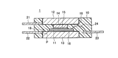
- FIG. 1 is a cross-sectional view showing the semiconductor device of this embodiment.
- a semiconductor element 11 is sandwiched between a first electrode 12 and a second electrode 13, and a block electrode 14 is disposed between the semiconductor element 11 and the first electrode 12.
- the first electrode 12 and the second electrode 13 are provided as an emitter electrode and a collector electrode, which are the main electrodes of the semiconductor element 11, and further function as a heat radiating plate. It is made of a good metal such as copper or aluminum.
- the block electrode 14 is integrally formed with the first electrode 12 by a cold spray method.
- Solder layers 15 and 16 are provided between the semiconductor element 11 and the second electrode 13 and the block electrode 14, and are joined to each other.
- Main electrode terminals 21 and 22 are connected to the first electrode 12 and the second electrode 13, respectively, and a bonding wire 24 is connected between the control electrode terminal 23 and the semiconductor element 11.
- the whole is sealed with a sealing resin 10.
- the first electrode 12 and the second electrode 13 are examples of the substrate described in the claims, and a resin bonding film 18 is formed on the surface thereof by a cold spray method.
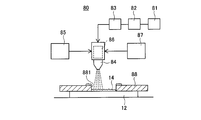
- FIG. 2 is a diagram conceptually showing the configuration of a film forming apparatus that executes the cold spray method.
- the film forming apparatus 80 has a compressor 81 for supplying compressed gas, and the compressed gas sent from the compressor 81 is heated by the heating means 82 and is injected from the nozzle 84 via the pressure adjusting valve 83. Yes.
- the powder tank 85 is filled with, for example, copper powder, and a heater 86 is provided so that the copper powder fed from the powder tank 85 can be heated by the nozzle 84.
- a driving means 87 for moving the nozzle 84 in parallel is provided.
- the mask 88 is disposed on the first electrode 12.
- the mask 88 is formed with an opening frame 881 having a size corresponding to the film formation region, and the position of the opening frame 881 is aligned with the first electrode 12.
- the nozzle 84 is supplied with copper powder having an average particle diameter of 5 to 60 ⁇ m from the powder tank 85, and the copper powder is heated by the heater 86. Further, the compressed gas heated from the compressor 81 is fed into the nozzle 84.
- the formation of the resin bonding film 18 by the cold spray method performed on the surfaces of the first electrode 12 and the second electrode 13 will be described.
- peeling of the sealing resin 10 is caused by a cooling / heating cycle.
- the cure shrinkage in which the volume shrinks due to the crosslinking reaction when the epoxy resin is cured at high temperature and the heat shrinkage when cooled from the high curing temperature to room temperature are combined. It was also found that the stress for peeling off the adhesion with the electrodes 12 and 13 was very large.
- the two electrodes 12 and 13 are arranged at a certain distance by a block electrode 14, and a sealing resin 10 is enclosed between them. Is done.
- the sealing resin 10 between the electrodes 12 and 13 is cured and shrunk, the opposing electrodes on both sides are thereby brought closer to reduce the distance between them, but the block electrode 14 between them prevents this.
- stress that promotes peeling acts on the bonding interface between the sealing resin 10 and the electrodes 12 and 13, and the sealing resin 10 is peeled off due to insufficient adhesive force.
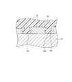
- FIG. 3 is an enlarged cross-sectional view of a P portion of FIG. 1 and showing a boundary portion between the second electrode 13 and the sealing resin 10.
- the resin bonding film 18 is formed by a cold spray method, and in particular, a recess 181 that is a space into which the sealing resin 10 enters is formed.
- the recess 181 is formed so that a space extends in the depth direction from the film surface. Specifically, the opening portion side of the surface is narrowed by the step, and the anchor portion 101 of the sealing resin 10 that has entered and hardened is caught and cannot be removed.
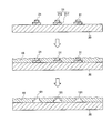
- FIG. 4 is a conceptual diagram showing the formation process of the resin bonding film 18.
- a two-stage resist block 31 for forming a space of the recess 181 is formed on the substrate 30 corresponding to the first electrode 12 and the second electrode 13.
- a photolithography technique is used, a photoresist is applied to the substrate 30, and then ultraviolet rays are irradiated from above the mask.
- the photoresist in the chemically changed portion is melted, and a resist block 31 is formed.
- a lower layer block 311 and an upper layer block 312 are formed in order, and the area of the lower layer block 311 is larger than that of the upper layer block 312.
- the resin bonding film 18 is formed by the cold spray method using the film forming apparatus 80 described above.
- the resin bonding film 18 having a predetermined thickness is formed so as to fill the resist block 31 on the surface of the substrate 30.
- the resist block 31 embedded in the resin bonding film 18 is removed by ashing using oxygen plasma or the like.
- impurities such as metals and organic substances are removed by washing with a solution such as an acid.
- a concave portion 181 having a space extending in the depth direction from the opening side of the surface is formed.
- the resin bonding film 18 with respect to the first electrode 12 and the second electrode 13 of the semiconductor device 1 has a recess 181 formed around the semiconductor element 11 and the block electrode 14 disposed in the center thereof.
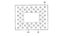
- 5 to 7 are plan views showing examples of the recesses formed in the resin bonding film 18 of the second electrode 13.
- An example of the recess 181 is a rectangular hole as shown in FIG. 5, and a plurality of the recesses 181 are arranged so as to surround the bonding region 131 of the semiconductor element 11.
- Another example of the recess 181 may be a plurality of grooves surrounding the bonding region 131 as shown in FIG.
- a rectangular groove having a dimension larger than the groove width may be combined with an annular groove surrounding the bonding region 131.
- the resin bonding film 18 is formed on the surfaces of the first and second electrodes 12 and 13, and as illustrated in FIG. 3, the sealing resin 10 is formed from the resin bonding film 18. Adhere to.
- the anchor portion 101 that has entered the recess 181 improves the adhesive strength against the stress that causes the sealing resin 10 to peel off.
- the resin bonding film 18 formed by the cold spray method is porous, the surface is uneven. Therefore, the bonding strength can also be improved by the sealing resin 10 entering the recessed portion of the surface of the resin bonding film 18.
- the block electrode 14 is also formed by the cold spray method, the bonding strength between the sealing resin 10 and the block electrode 14 is improved.
- the concave portion 181 of the resin bonding film 18 improves the bonding strength of the sealing resin 10 when the sealing resin 10 that has entered the hole spreads and adheres in all directions.
- the concave portion 181 is the groove shown in FIG. 6, the sealing resin 10 that has entered the concave portion 181 flows to the corner of the groove. Therefore, the internal bubbles can be pushed out to form the anchor portion 101 filled with resin, and the adhesion can be ensured.
- the recessed part 181 is what combined the hole and groove
- the bonding strength by the resin bonding film 18 by improving the bonding strength by the resin bonding film 18, it is possible to abolish the conventional application of polyamide resin or the like and the formation of a sprayed coating made of aluminum, etc., reducing the material cost, improving the productivity, etc. Thus, the cost of the semiconductor device 1 can be reduced.
- the concave portion 181 since the formation of the concave portion 181 does not cause distortion such as a punching process, the concave portion 181 can be formed in the second electrode 13 near the semiconductor element 11.
- the resin bonding film 18 can be formed on the entire second electrode 13 by being formed of a metal such as aluminum or copper having good thermal conductivity and electrical conductivity. Therefore, the adhesiveness between the resin bonding film 18 and the sealing resin 10 can be ensured in the immediate vicinity of the semiconductor element 11.
- the three-dimensional molding of the resin bonding film 18 can be easily and uniformly performed, and can be soldered as it is. Since the resin bonding film 18 is made of copper, nickel, silver, or copper, soldering can be performed, so the nickel plating and gold plating that have been applied to the first and second electrodes 12 and 13 are unnecessary. become. Nickel plating causes a decrease in adhesion to the sealing resin, and gold plating is very expensive. In this respect as well, the price of the semiconductor device 1 can be reduced.
- the block electrode 14 and the resin bonding film 18 formed by the cold spray method cause capillary action due to the unevenness of the surface. Therefore, surplus solder is absorbed in the recesses, so that the excess solder can be prevented from protruding, and there are effects such as preventing the solder from forming droplets and adhering to the extra portions.
- the semiconductor device 1 for double-sided cooling is shown and described in FIG. 1, but it may be a semiconductor device for single-sided cooling in which electrodes are provided only on one side of the semiconductor element.
- the concave portion 181 has been described by taking a rectangular hole as an example, but other shapes such as a round shape may be used.
Landscapes
- Chemical & Material Sciences (AREA)
- Chemical Kinetics & Catalysis (AREA)
- Engineering & Computer Science (AREA)
- Materials Engineering (AREA)
- Mechanical Engineering (AREA)
- Metallurgy (AREA)
- Organic Chemistry (AREA)
- Structures Or Materials For Encapsulating Or Coating Semiconductor Devices Or Solid State Devices (AREA)
- Encapsulation Of And Coatings For Semiconductor Or Solid State Devices (AREA)
Abstract
Description
また、上記半導体装置は、前記基板が、前記半導体素子の両方の面に配置された第1電極と第2電極であり、前記半導体素子と前記第1電極の間に配置されたブロック電極が存在し、そのブロック電極が前記第1電極に対してコールドスプレー法によって成膜されたものであることが好ましい。
また、上記半導体装置は、前記凹部が、前記半導体素子や前記ブロック電極の周りを囲むように配置された複数の穴であることが好ましい。
また、上記半導体装置は、前記凹部が、前記半導体素子や前記ブロック電極の周りを囲む溝であることが好ましい。
また、上記半導体装置は、前記凹部が、前記半導体素子や前記ブロック電極の周りを囲む溝に重ねて、その溝幅より寸法の大きい矩形の穴が形成されたものであることが好ましい。
10 樹脂
11 半導体素子
12 第1電極
13 第2電極
14 ブロック電極
15,16 半田層
18 樹脂接合膜
101 アンカー部
181 凹部
例えば、図1には両面冷却用の半導体装置1を示して説明したが、半導体素子の片側にのみ電極を設ける片面冷却用の半導体装置であってもよい。
また、例えば、図5及び図7では、凹部181の形状として矩形の穴を例に挙げて説明したが、丸形状など、その他の形状であってもよい。
Claims (6)
- 半導体素子と、その半導体素子の一方の面又は両方の面に対向して配置された一枚又は二枚の基板とが、樹脂によって封止された半導体装置において、
前記基板の一方又は両方に、コールドスプレー法によって金属の粉末を吹き付けて成膜した樹脂接合膜が形成され、その樹脂接合膜には、膜表面から深さ方向に空間が広がるようにした凹部が形成されたものであることを特徴とする半導体装置。 - 請求項1に記載する半導体装置において、
前記凹部は、段状に形成されたものであることを特徴とする半導体装置。 - 請求項1又は請求項2に記載する半導体装置において、
前記基板は、前記半導体素子の両方の面に配置された第1電極と第2電極であり、前記半導体素子と前記第1電極の間に配置されたブロック電極が存在し、そのブロック電極が前記第1電極に対してコールドスプレー法によって成膜されものであることを特徴とする半導体装置。 - 請求項1乃至請求項3のいずれかに記載する半導体装置において、
前記凹部は、前記半導体素子や前記ブロック電極の周りを囲むように配置された複数の穴であることを特徴とする半導体装置。 - 請求項1乃至請求項3のいずれかに記載する半導体装置において、
前記凹部は、前記半導体素子や前記ブロック電極の周りを囲む溝であることを特徴とする半導体装置。 - 請求項1乃至請求項3のいずれかに記載する半導体装置において、
前記凹部は、前記半導体素子や前記ブロック電極の周りを囲む溝に重ねて、その溝幅より寸法の大きい矩形の穴が形成されたものであることを特徴とする半導体装置。
Priority Applications (6)
| Application Number | Priority Date | Filing Date | Title |
|---|---|---|---|
| EP10851766.5A EP2573810B1 (en) | 2010-05-21 | 2010-05-21 | Semiconductor device |
| CN201080055269.XA CN102652357B (zh) | 2010-05-21 | 2010-05-21 | 半导体装置 |
| KR1020127014542A KR101297870B1 (ko) | 2010-05-21 | 2010-05-21 | 반도체 장치 |
| US13/499,253 US8436461B2 (en) | 2010-05-21 | 2010-05-21 | Semiconductor device |
| PCT/JP2010/058586 WO2011145202A1 (ja) | 2010-05-21 | 2010-05-21 | 半導体装置 |
| JP2010544107A JP5321601B2 (ja) | 2010-05-21 | 2010-05-21 | 半導体装置 |
Applications Claiming Priority (1)
| Application Number | Priority Date | Filing Date | Title |
|---|---|---|---|
| PCT/JP2010/058586 WO2011145202A1 (ja) | 2010-05-21 | 2010-05-21 | 半導体装置 |
Publications (1)
| Publication Number | Publication Date |
|---|---|
| WO2011145202A1 true WO2011145202A1 (ja) | 2011-11-24 |
Family
ID=44991326
Family Applications (1)
| Application Number | Title | Priority Date | Filing Date |
|---|---|---|---|
| PCT/JP2010/058586 Ceased WO2011145202A1 (ja) | 2010-05-21 | 2010-05-21 | 半導体装置 |
Country Status (6)
| Country | Link |
|---|---|
| US (1) | US8436461B2 (ja) |
| EP (1) | EP2573810B1 (ja) |
| JP (1) | JP5321601B2 (ja) |
| KR (1) | KR101297870B1 (ja) |
| CN (1) | CN102652357B (ja) |
| WO (1) | WO2011145202A1 (ja) |
Cited By (8)
| Publication number | Priority date | Publication date | Assignee | Title |
|---|---|---|---|---|
| JP2014139968A (ja) * | 2013-01-21 | 2014-07-31 | Toyota Motor Corp | 半導体装置およびその製造方法 |
| WO2014129061A1 (ja) * | 2013-02-19 | 2014-08-28 | 三菱重工業株式会社 | 成膜方法 |
| CN104956535A (zh) * | 2013-01-29 | 2015-09-30 | 丰田自动车株式会社 | 电池 |
| JP2015211157A (ja) * | 2014-04-28 | 2015-11-24 | 三菱電機株式会社 | パワー半導体モジュールおよびその製造方法 |
| JP2016152386A (ja) * | 2015-02-19 | 2016-08-22 | 三菱マテリアル株式会社 | パワーモジュール用基板及びパワーモジュール |
| JP2018507555A (ja) * | 2015-02-04 | 2018-03-15 | シーメンス アクチエンゲゼルシヤフトSiemens Aktiengesellschaft | マスクを用いてコールドガススプレーする方法 |
| WO2021193643A1 (ja) * | 2020-03-25 | 2021-09-30 | 国立大学法人東北大学 | 複合部材の製造方法および複合部材 |
| JP2021154733A (ja) * | 2020-03-25 | 2021-10-07 | 国立大学法人東北大学 | 複合部材の製造方法および複合部材 |
Families Citing this family (5)
| Publication number | Priority date | Publication date | Assignee | Title |
|---|---|---|---|---|
| CN102549738B (zh) * | 2010-05-18 | 2015-07-01 | 丰田自动车株式会社 | 半导体装置及其制造方法 |
| KR102424402B1 (ko) | 2015-08-13 | 2022-07-25 | 삼성전자주식회사 | 반도체 패키지 및 그 제조방법 |
| USD926234S1 (en) | 2018-05-24 | 2021-07-27 | Whirlpool Corporation | Kitchen appliance with two-dimensional applied surface graphic |
| JP7680240B2 (ja) * | 2021-03-30 | 2025-05-20 | ローム株式会社 | 半導体装置 |
| KR102866116B1 (ko) | 2021-11-26 | 2025-09-30 | 삼성전자주식회사 | 반도체 패키지 |
Citations (6)
| Publication number | Priority date | Publication date | Assignee | Title |
|---|---|---|---|---|
| JPH03280452A (ja) * | 1990-03-29 | 1991-12-11 | Seiko Epson Corp | 半導体装置 |
| JPH06112390A (ja) | 1992-09-24 | 1994-04-22 | Nippon Steel Corp | リードフレーム |
| JP2002289739A (ja) * | 2001-03-23 | 2002-10-04 | Dainippon Printing Co Ltd | 樹脂封止型半導体装置および半導体装置用回路部材とその製造方法 |
| JP2003124406A (ja) * | 2001-08-06 | 2003-04-25 | Denso Corp | 半導体装置 |
| JP2006319146A (ja) * | 2005-05-13 | 2006-11-24 | Fuji Electric Holdings Co Ltd | 配線基板 |
| JP2007258587A (ja) | 2006-03-24 | 2007-10-04 | Rohm Co Ltd | リードフレームおよびその製造方法並びにリードフレームを備えた半導体装置 |
Family Cites Families (5)
| Publication number | Priority date | Publication date | Assignee | Title |
|---|---|---|---|---|
| JP4248037B2 (ja) * | 1997-02-04 | 2009-04-02 | 株式会社不二機販 | 金属被膜の形成方法 |
| JP3719506B2 (ja) | 2001-12-19 | 2005-11-24 | 株式会社デンソー | 半導体装置及びその製造方法 |
| JP3748849B2 (ja) * | 2002-12-06 | 2006-02-22 | 三菱電機株式会社 | 樹脂封止型半導体装置 |
| JP4241859B2 (ja) | 2007-07-19 | 2009-03-18 | トヨタ自動車株式会社 | パワーモジュールの製造方法、パワーモジュール、車両用インバータ、及び車両 |
| KR101438826B1 (ko) * | 2008-06-23 | 2014-09-05 | 엘지이노텍 주식회사 | 발광장치 |
-
2010
- 2010-05-21 CN CN201080055269.XA patent/CN102652357B/zh not_active Expired - Fee Related
- 2010-05-21 KR KR1020127014542A patent/KR101297870B1/ko not_active Expired - Fee Related
- 2010-05-21 JP JP2010544107A patent/JP5321601B2/ja not_active Expired - Fee Related
- 2010-05-21 EP EP10851766.5A patent/EP2573810B1/en not_active Not-in-force
- 2010-05-21 WO PCT/JP2010/058586 patent/WO2011145202A1/ja not_active Ceased
- 2010-05-21 US US13/499,253 patent/US8436461B2/en not_active Expired - Fee Related
Patent Citations (6)
| Publication number | Priority date | Publication date | Assignee | Title |
|---|---|---|---|---|
| JPH03280452A (ja) * | 1990-03-29 | 1991-12-11 | Seiko Epson Corp | 半導体装置 |
| JPH06112390A (ja) | 1992-09-24 | 1994-04-22 | Nippon Steel Corp | リードフレーム |
| JP2002289739A (ja) * | 2001-03-23 | 2002-10-04 | Dainippon Printing Co Ltd | 樹脂封止型半導体装置および半導体装置用回路部材とその製造方法 |
| JP2003124406A (ja) * | 2001-08-06 | 2003-04-25 | Denso Corp | 半導体装置 |
| JP2006319146A (ja) * | 2005-05-13 | 2006-11-24 | Fuji Electric Holdings Co Ltd | 配線基板 |
| JP2007258587A (ja) | 2006-03-24 | 2007-10-04 | Rohm Co Ltd | リードフレームおよびその製造方法並びにリードフレームを備えた半導体装置 |
Non-Patent Citations (1)
| Title |
|---|
| See also references of EP2573810A4 |
Cited By (12)
| Publication number | Priority date | Publication date | Assignee | Title |
|---|---|---|---|---|
| JP2014139968A (ja) * | 2013-01-21 | 2014-07-31 | Toyota Motor Corp | 半導体装置およびその製造方法 |
| CN104956535A (zh) * | 2013-01-29 | 2015-09-30 | 丰田自动车株式会社 | 电池 |
| WO2014129061A1 (ja) * | 2013-02-19 | 2014-08-28 | 三菱重工業株式会社 | 成膜方法 |
| JP2014159611A (ja) * | 2013-02-19 | 2014-09-04 | Mitsubishi Heavy Ind Ltd | 成膜方法 |
| US9677165B2 (en) | 2013-02-19 | 2017-06-13 | Mitsubishi Heavy Industries, Ltd. | Film growing method |
| JP2015211157A (ja) * | 2014-04-28 | 2015-11-24 | 三菱電機株式会社 | パワー半導体モジュールおよびその製造方法 |
| JP2018507555A (ja) * | 2015-02-04 | 2018-03-15 | シーメンス アクチエンゲゼルシヤフトSiemens Aktiengesellschaft | マスクを用いてコールドガススプレーする方法 |
| US10648085B2 (en) | 2015-02-04 | 2020-05-12 | Siemens Aktiengesellschaft | Cold gas dynamic spraying using a mask |
| JP2016152386A (ja) * | 2015-02-19 | 2016-08-22 | 三菱マテリアル株式会社 | パワーモジュール用基板及びパワーモジュール |
| WO2021193643A1 (ja) * | 2020-03-25 | 2021-09-30 | 国立大学法人東北大学 | 複合部材の製造方法および複合部材 |
| JP2021154733A (ja) * | 2020-03-25 | 2021-10-07 | 国立大学法人東北大学 | 複合部材の製造方法および複合部材 |
| US12479188B2 (en) | 2020-03-25 | 2025-11-25 | Tohoku University | Method for manufacturing composite member, and composite member |
Also Published As
| Publication number | Publication date |
|---|---|
| US20120181685A1 (en) | 2012-07-19 |
| CN102652357B (zh) | 2015-09-09 |
| JP5321601B2 (ja) | 2013-10-23 |
| EP2573810A4 (en) | 2014-04-30 |
| KR20120091297A (ko) | 2012-08-17 |
| EP2573810B1 (en) | 2016-08-17 |
| JPWO2011145202A1 (ja) | 2013-07-22 |
| US8436461B2 (en) | 2013-05-07 |
| KR101297870B1 (ko) | 2013-08-19 |
| CN102652357A (zh) | 2012-08-29 |
| EP2573810A1 (en) | 2013-03-27 |
Similar Documents
| Publication | Publication Date | Title |
|---|---|---|
| JP5321601B2 (ja) | 半導体装置 | |
| JP5565315B2 (ja) | 半導体装置の製造方法 | |
| US6693350B2 (en) | Semiconductor device having radiation structure and method for manufacturing semiconductor device having radiation structure | |
| US8558367B2 (en) | Semiconductor module | |
| JP6309112B2 (ja) | パワーモジュール | |
| JP4844702B1 (ja) | マスキング治具、基板加熱装置、及び成膜方法 | |
| JP6619356B2 (ja) | 電力用半導体装置およびその製造方法 | |
| JP4023397B2 (ja) | 半導体モジュールおよびその製造方法 | |
| JP2010171271A (ja) | 半導体装置およびその製造方法 | |
| CN107424971A (zh) | 芯片载体上基于腔体的特征 | |
| WO2011092859A1 (ja) | 半導体装置の製造方法および半導体装置 | |
| JP5983249B2 (ja) | 半導体モジュールの製造方法 | |
| JP2011054889A (ja) | 樹脂封止型半導体装置およびその製造方法 | |
| JP4363324B2 (ja) | 半導体モジュール | |
| JP3719506B2 (ja) | 半導体装置及びその製造方法 | |
| JP4631205B2 (ja) | 半導体装置及びその製造方法 | |
| JP2013168421A (ja) | 配線基板および配線基板の製造方法 | |
| JP2020077857A (ja) | モジュールおよびその製造方法 | |
| JP4024458B2 (ja) | 半導体装置の実装方法および半導体装置実装体の製造方法 | |
| JP4492257B2 (ja) | 半導体モジュールおよびその製造方法 | |
| JP5035265B2 (ja) | 電子部品実装構造体の製造方法 | |
| JP2011249599A (ja) | 半導体実装基板およびそれを用いた実装構造体 | |
| WO1995032520A1 (fr) | Montage de composants electroniques et son procede de realisation | |
| JP2013191722A (ja) | 配線基板および配線基板の製造方法 |
Legal Events
| Date | Code | Title | Description |
|---|---|---|---|
| WWE | Wipo information: entry into national phase |
Ref document number: 201080055269.X Country of ref document: CN |
|
| WWE | Wipo information: entry into national phase |
Ref document number: 2010544107 Country of ref document: JP |
|
| 121 | Ep: the epo has been informed by wipo that ep was designated in this application |
Ref document number: 10851766 Country of ref document: EP Kind code of ref document: A1 |
|
| REEP | Request for entry into the european phase |
Ref document number: 2010851766 Country of ref document: EP |
|
| WWE | Wipo information: entry into national phase |
Ref document number: 2010851766 Country of ref document: EP |
|
| WWE | Wipo information: entry into national phase |
Ref document number: 13499253 Country of ref document: US |
|
| ENP | Entry into the national phase |
Ref document number: 20127014542 Country of ref document: KR Kind code of ref document: A |
|
| NENP | Non-entry into the national phase |
Ref country code: DE |