WO2011145676A1 - タッチセンサ付き表示装置 - Google Patents
タッチセンサ付き表示装置 Download PDFInfo
- Publication number
- WO2011145676A1 WO2011145676A1 PCT/JP2011/061497 JP2011061497W WO2011145676A1 WO 2011145676 A1 WO2011145676 A1 WO 2011145676A1 JP 2011061497 W JP2011061497 W JP 2011061497W WO 2011145676 A1 WO2011145676 A1 WO 2011145676A1
- Authority
- WO
- WIPO (PCT)
- Prior art keywords
- sensor
- signal
- period
- pixel circuit
- correction data
- Prior art date
- Legal status (The legal status is an assumption and is not a legal conclusion. Google has not performed a legal analysis and makes no representation as to the accuracy of the status listed.)
- Ceased
Links
Images












Classifications
-
- G—PHYSICS
- G09—EDUCATION; CRYPTOGRAPHY; DISPLAY; ADVERTISING; SEALS
- G09G—ARRANGEMENTS OR CIRCUITS FOR CONTROL OF INDICATING DEVICES USING STATIC MEANS TO PRESENT VARIABLE INFORMATION
- G09G3/00—Control arrangements or circuits, of interest only in connection with visual indicators other than cathode-ray tubes
- G09G3/20—Control arrangements or circuits, of interest only in connection with visual indicators other than cathode-ray tubes for presentation of an assembly of a number of characters, e.g. a page, by composing the assembly by combination of individual elements arranged in a matrix no fixed position being assigned to or needed to be assigned to the individual characters or partial characters
- G09G3/34—Control arrangements or circuits, of interest only in connection with visual indicators other than cathode-ray tubes for presentation of an assembly of a number of characters, e.g. a page, by composing the assembly by combination of individual elements arranged in a matrix no fixed position being assigned to or needed to be assigned to the individual characters or partial characters by control of light from an independent source
- G09G3/3406—Control of illumination source
-
- G—PHYSICS
- G02—OPTICS
- G02F—OPTICAL DEVICES OR ARRANGEMENTS FOR THE CONTROL OF LIGHT BY MODIFICATION OF THE OPTICAL PROPERTIES OF THE MEDIA OF THE ELEMENTS INVOLVED THEREIN; NON-LINEAR OPTICS; FREQUENCY-CHANGING OF LIGHT; OPTICAL LOGIC ELEMENTS; OPTICAL ANALOGUE/DIGITAL CONVERTERS
- G02F1/00—Devices or arrangements for the control of the intensity, colour, phase, polarisation or direction of light arriving from an independent light source, e.g. switching, gating or modulating; Non-linear optics
- G02F1/01—Devices or arrangements for the control of the intensity, colour, phase, polarisation or direction of light arriving from an independent light source, e.g. switching, gating or modulating; Non-linear optics for the control of the intensity, phase, polarisation or colour
- G02F1/13—Devices or arrangements for the control of the intensity, colour, phase, polarisation or direction of light arriving from an independent light source, e.g. switching, gating or modulating; Non-linear optics for the control of the intensity, phase, polarisation or colour based on liquid crystals, e.g. single liquid crystal display cells
- G02F1/133—Constructional arrangements; Operation of liquid crystal cells; Circuit arrangements
- G02F1/1333—Constructional arrangements; Manufacturing methods
- G02F1/13338—Input devices, e.g. touch panels
-
- G—PHYSICS
- G02—OPTICS
- G02F—OPTICAL DEVICES OR ARRANGEMENTS FOR THE CONTROL OF LIGHT BY MODIFICATION OF THE OPTICAL PROPERTIES OF THE MEDIA OF THE ELEMENTS INVOLVED THEREIN; NON-LINEAR OPTICS; FREQUENCY-CHANGING OF LIGHT; OPTICAL LOGIC ELEMENTS; OPTICAL ANALOGUE/DIGITAL CONVERTERS
- G02F1/00—Devices or arrangements for the control of the intensity, colour, phase, polarisation or direction of light arriving from an independent light source, e.g. switching, gating or modulating; Non-linear optics
- G02F1/01—Devices or arrangements for the control of the intensity, colour, phase, polarisation or direction of light arriving from an independent light source, e.g. switching, gating or modulating; Non-linear optics for the control of the intensity, phase, polarisation or colour
- G02F1/13—Devices or arrangements for the control of the intensity, colour, phase, polarisation or direction of light arriving from an independent light source, e.g. switching, gating or modulating; Non-linear optics for the control of the intensity, phase, polarisation or colour based on liquid crystals, e.g. single liquid crystal display cells
- G02F1/133—Constructional arrangements; Operation of liquid crystal cells; Circuit arrangements
- G02F1/135—Liquid crystal cells structurally associated with a photoconducting or a ferro-electric layer, the properties of which can be optically or electrically varied
- G02F1/1354—Liquid crystal cells structurally associated with a photoconducting or a ferro-electric layer, the properties of which can be optically or electrically varied having a particular photoconducting structure or material
-
- G—PHYSICS
- G06—COMPUTING OR CALCULATING; COUNTING
- G06F—ELECTRIC DIGITAL DATA PROCESSING
- G06F3/00—Input arrangements for transferring data to be processed into a form capable of being handled by the computer; Output arrangements for transferring data from processing unit to output unit, e.g. interface arrangements
- G06F3/01—Input arrangements or combined input and output arrangements for interaction between user and computer
- G06F3/03—Arrangements for converting the position or the displacement of a member into a coded form
- G06F3/041—Digitisers, e.g. for touch screens or touch pads, characterised by the transducing means
- G06F3/042—Digitisers, e.g. for touch screens or touch pads, characterised by the transducing means by opto-electronic means
-
- G—PHYSICS
- G02—OPTICS
- G02F—OPTICAL DEVICES OR ARRANGEMENTS FOR THE CONTROL OF LIGHT BY MODIFICATION OF THE OPTICAL PROPERTIES OF THE MEDIA OF THE ELEMENTS INVOLVED THEREIN; NON-LINEAR OPTICS; FREQUENCY-CHANGING OF LIGHT; OPTICAL LOGIC ELEMENTS; OPTICAL ANALOGUE/DIGITAL CONVERTERS
- G02F1/00—Devices or arrangements for the control of the intensity, colour, phase, polarisation or direction of light arriving from an independent light source, e.g. switching, gating or modulating; Non-linear optics
- G02F1/01—Devices or arrangements for the control of the intensity, colour, phase, polarisation or direction of light arriving from an independent light source, e.g. switching, gating or modulating; Non-linear optics for the control of the intensity, phase, polarisation or colour
- G02F1/13—Devices or arrangements for the control of the intensity, colour, phase, polarisation or direction of light arriving from an independent light source, e.g. switching, gating or modulating; Non-linear optics for the control of the intensity, phase, polarisation or colour based on liquid crystals, e.g. single liquid crystal display cells
- G02F1/133—Constructional arrangements; Operation of liquid crystal cells; Circuit arrangements
- G02F1/13306—Circuit arrangements or driving methods for the control of single liquid crystal cells
- G02F1/13312—Circuits comprising photodetectors for purposes other than feedback
-
- G—PHYSICS
- G09—EDUCATION; CRYPTOGRAPHY; DISPLAY; ADVERTISING; SEALS
- G09G—ARRANGEMENTS OR CIRCUITS FOR CONTROL OF INDICATING DEVICES USING STATIC MEANS TO PRESENT VARIABLE INFORMATION
- G09G2360/00—Aspects of the architecture of display systems
- G09G2360/14—Detecting light within display terminals, e.g. using a single or a plurality of photosensors
- G09G2360/145—Detecting light within display terminals, e.g. using a single or a plurality of photosensors the light originating from the display screen
Definitions
- the present invention relates to a display device having a photodetection element such as a photodiode in a pixel, and more particularly to a display device capable of automatically correcting a photosensor signal during operation of the display device.
- a method of providing a plurality of optical sensors on a display panel and providing an input function such as a touch panel, a pen input, and a scanner is known for display devices.
- an input function such as a touch panel, a pen input, and a scanner.
- a method is also known in which a component that depends on the light environment is removed from a signal detected by an optical sensor and a signal to be originally input is obtained.
- the backlight blinks once in one frame period, and the amount of light in the backlight lighting period in one frame period. It is described that the light receiving elements are reset and read out in a line-sequential manner so that the amount of light in the backlight off period is obtained from all the light receiving elements.
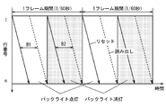
- FIG. 25 is a diagram showing the lighting and extinguishing timings of the backlight described in Japanese Patent No. 4072732 and the resetting and reading timings of the light receiving elements.
- the backlight is turned on in the first half of one frame period and turned off in the second half.
- the light receiving elements are reset line-sequentially (solid line arrows), and then reading from the light-receiving elements is line-sequentially (dashed line arrows). Even during the backlight off period, the light receiving element is reset and read out in the same manner.
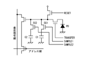
- Japanese Patent No. 3521187 describes a solid-state imaging device having a unit light receiving section shown in FIG.
- the unit light receiving unit shown in FIG. 26 includes one photoelectric conversion unit PD and two charge storage units C1 and C2.
- the first sample gate SG1 is turned on, and the charge generated by the photoelectric conversion unit PD is stored in the first charge storage unit C1.
- the second sample gate SG2 is turned on, and the charges generated by the photoelectric conversion unit PD are accumulated in the second charge accumulation unit C2.
- a display device in which a plurality of photosensors are provided on a display panel, readout from the photosensors is performed in a line sequential manner.
- the backlight for the mobile device is turned on at the same time as the entire screen and turned off at the same time.
- the input / output device described in Japanese Patent No. 4072732 blinks the backlight once in one frame period, performs reset and readout in a period that does not overlap in the backlight lighting period, and overlaps reset and readout in the backlight off period. Do it in a period not to be. For this reason, it is necessary to perform reading from the light receiving element within a 1 ⁇ 4 frame period (for example, within 1/240 seconds when the frame rate is 60 frames / second). However, it is actually quite difficult to perform such high-speed reading.
- this input / output device detects the light quantity during the backlight lighting period and the light quantity during the backlight extinguishing period by the same light receiving element. For this reason, when the amount of light in the backlight lighting period is detected in a certain light receiving element, the detection of the amount of light in the backlight extinction period cannot be started in the light receiving element until the detected amount of light is read from the light receiving element.
- an object of the present invention is to solve the above-mentioned problems and to provide a display device having an input function that does not depend on the light environment.
- a display device disclosed herein is a display device including an active matrix substrate, and is connected to the photosensor provided in a pixel region of the active matrix substrate and the photosensor.
- a sensor drive wiring that supplies a sensor drive signal to the optical sensor via the sensor drive wiring, and amplifies a signal read from the optical sensor in accordance with the sensor drive signal.
- An amplifier circuit that outputs a signal; a signal processing circuit that processes an optical sensor signal output from the amplifier circuit; and a light source for the optical sensor, wherein the optical sensor includes the light source according to the sensor drive signal.
- a first sensor that accumulates charges according to the amount of received light during the accumulation period at the time of lighting, and outputs a sensor signal according to the accumulated charges when the readout period comes.
- a second sensor pixel circuit that accumulates charges according to the amount of received light during the accumulation period when the light source is turned off and outputs a sensor signal according to the accumulated charges when the readout period arrives.
- a sensor driving mode for obtaining the sensor signal from each of the first sensor pixel circuit and the second sensor pixel circuit of the photosensor as an operation mode of one frame period,
- a first correction data acquisition mode for acquiring first correction data for correcting a sensor signal obtained from the first sensor pixel circuit using a sensor drive signal different from the sensor drive mode;
- a second correction data for correcting the sensor signal obtained from the second sensor pixel circuit using a sensor drive signal different from the drive mode.
- a second correction data acquisition mode for acquiring data and an accumulation period when the light source is turned on in the first correction data acquisition mode is greater than an accumulation period when the light source is turned on in the sensor drive mode.
- the storage period when the light source is turned off in the second correction data acquisition mode is shorter than the storage period when the light source is turned off in the sensor drive mode.
- a display device having a photodetection element in a pixel and in particular, a display device having an input function independent of the light environment.
- FIG. 1 is a block diagram showing a configuration of a display device according to an embodiment of the present invention.
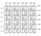
- FIG. 2 is a diagram showing an arrangement of sensor pixel circuits in a display panel included in the display device shown in FIG.
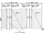
- FIG. 3 is a diagram showing the timing of turning on and off the backlight and the reset and readout timing for the sensor pixel circuit in the display device shown in FIG.
- FIG. 4 is a signal waveform diagram of the display panel in the display device shown in FIG.
- FIG. 5 is a diagram showing a schematic configuration of a sensor pixel circuit included in the display device shown in FIG.
- FIG. 6 is a circuit diagram of the sensor pixel circuit according to the first embodiment of the present invention.
- FIG. 7 is a layout diagram of the sensor pixel circuit shown in FIG. FIG.
- FIG. 8 is a diagram showing the operation of the sensor pixel circuit shown in FIG.
- FIG. 9 is a signal waveform diagram of the sensor pixel circuit shown in FIG.
- FIG. 10 is a timing chart showing an example of a drive signal in the sensor drive mode, a drive signal in the first correction data acquisition mode, and a drive signal in the second correction data acquisition mode.
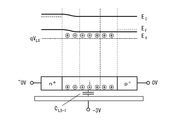
- FIG. 11 is a timing chart showing another example of the drive signal in the sensor drive mode, the drive signal in the first correction data acquisition mode, and the drive signal in the second correction data acquisition mode.
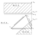
- FIG. 12 is a schematic sectional view of a diode.
- FIG. 13 is a diagram showing the distribution of the modes A, B, and C of the diode by the relationship between the anode potential V A and the potential V LS of the light shielding film LS.
- FIG. 14A is a schematic diagram showing the charge distribution of the diode in the mode B state.
- FIG. 14B is a schematic diagram showing the charge distribution of the diode in the mode A state.
- FIG. 15 is a circuit diagram of a sensor pixel circuit according to the second embodiment of the present invention.
- FIG. 16 is a layout diagram of the sensor pixel circuit shown in FIG.
- FIG. 17 is a diagram illustrating the operation of the sensor pixel circuit shown in FIG. 18 is a signal waveform diagram of the sensor pixel circuit shown in FIG. FIG.
- FIG. 19A is a circuit diagram of a sensor pixel circuit according to a first modification of the first embodiment.
- FIG. 19B is a circuit diagram of a sensor pixel circuit according to a second modification example of the first embodiment.
- FIG. 19C is a circuit diagram of a sensor pixel circuit according to a third modification example of the first embodiment.
- FIG. 19D is a circuit diagram of a sensor pixel circuit according to a fourth modification example of the first embodiment.
- FIG. 19E is a circuit diagram of a sensor pixel circuit according to a fifth modification example of the first embodiment.
- FIG. 20 is a diagram illustrating an operation of the sensor pixel circuit illustrated in FIG. 19C.
- FIG. 21 is a signal waveform diagram of the sensor pixel circuit shown in FIG. 19C.
- FIG. 22 is a diagram illustrating an operation of the sensor pixel circuit illustrated in FIG. 19D.
- FIG. 23 is a diagram illustrating an operation of the sensor pixel circuit illustrated in FIG. 19E.
- FIG. 24A is a circuit diagram of a sensor pixel circuit according to a first modification example of the second embodiment.
- FIG. 24B is a circuit diagram of a sensor pixel circuit according to a second modification example of the second embodiment.
- FIG. 24C is a circuit diagram of a sensor pixel circuit according to a third modification example of the second embodiment.
- FIG. 24D is a circuit diagram of a sensor pixel circuit according to a fourth modification example of the second embodiment.
- FIG. 24E is a circuit diagram of a sensor pixel circuit according to a fifth modification example of the second embodiment.
- FIG. 24A is a circuit diagram of a sensor pixel circuit according to a first modification example of the second embodiment.
- FIG. 24B is a circuit diagram of a sensor pixel circuit according to a second modification
- FIG. 25 is a diagram showing the lighting and extinguishing timing of the backlight and the resetting and reading timing for the light receiving element in the conventional input / output device.
- FIG. 26 is a circuit diagram of a unit light receiving unit included in a conventional solid-state imaging device.
- a display device is a display device including an active matrix substrate, and includes a photosensor provided in a pixel region of the active matrix substrate and a connection to the photosensor.
- Sensor drive wiring a sensor drive circuit for supplying a sensor drive signal to the optical sensor via the sensor drive wiring, a signal read from the photosensor in accordance with the sensor drive signal,
- An amplifier circuit that outputs as a sensor signal, a signal processing circuit that processes an optical sensor signal output from the amplifier circuit, and a light source for the optical sensor are provided.
- the photosensor According to the sensor drive signal, the photosensor accumulates charges according to the amount of received light during the accumulation period when the light source is turned on, and when the readout period comes, a sensor signal according to the accumulated charge is accumulated.
- the first sensor pixel circuit to be output and the sensor drive signal a charge corresponding to the amount of received light is accumulated during the accumulation period when the light source is turned off, and a sensor signal corresponding to the accumulated charge is output when the readout period comes.
- Sensor pixel circuit In the first configuration, the sensor driving circuit is configured to obtain a sensor signal from each of the first sensor pixel circuit and the second sensor pixel circuit of the photosensor as an operation mode for one frame period.
- a first correction data acquisition mode for acquiring first correction data for correcting a sensor signal obtained from the first sensor pixel circuit using a sensor drive signal different from the mode and the sensor drive mode
- a second correction data acquisition mode for acquiring second correction data for correcting a sensor signal obtained from the second sensor pixel circuit using a sensor drive signal different from the sensor drive mode.
- the light source lighting period in the first correction data acquisition mode is shorter than the light source lighting period in the sensor drive mode (second configuration).
- the light source lighting start timing in one frame period is preferably the same timing as the sensor drive mode (third configuration).
- the period from the start time of the accumulation period in the first correction data acquisition mode to the end time of the light source lighting period is from the start time of the accumulation period in the sensor drive mode. It is preferable that the period is shorter than the period until the end of the light source lighting period (fourth configuration).
- the length of the period from the end of the accumulation period to the end of the light source lighting period is equal to the length of the accumulation period in the sensor drive mode. It is preferable to be equal to the length of the period from the end point to the end point of the light source lighting period (fifth configuration).
- the light source lighting period in the second correction data acquisition mode is preferably longer than the light source lighting period in the first correction data acquisition mode (sixth configuration).
- the start and end timings of the light source lighting period in one frame period are the light source lighting period in one frame period in the sensor drive mode. It is preferable that the timing is the same as the start and end timing (seventh configuration).
- an optical sensor signal level obtained from the second sensor pixel circuit in the sensor driving mode is denoted as B
- the first sensor pixel circuit is expressed in the first correction data acquisition mode.
- B 1st the optical sensor signal level obtained from the first sensor pixel circuit in the second correction data acquisition mode
- the sensor drive circuit in the first correction data acquisition mode, supplies a read signal having an amplitude smaller than the amplitude of the read signal in the sensor drive mode.
- the gain correction optical sensor signal level W 1st is acquired
- the sensor drive circuit in the second correction data acquisition mode, outputs a read signal having an amplitude smaller than the amplitude of the read signal in the sensor drive mode.
- the signal processing circuit is controlled by the sensor driving mode from the first sensor pixel circuit.
- an optical sensor signal level obtained from the second sensor pixel circuit in the sensor driving mode is expressed as B, and the first sensor is acquired in the first correction data acquisition mode.
- the optical sensor signal level obtained from the pixel circuit is denoted as B 1st
- the optical sensor signal level obtained from the first sensor pixel circuit in the second correction data acquisition mode is denoted as B 2nd
- the first In the correction data acquisition mode the sensor driving circuit acquires a gain correction optical sensor signal level W 1st by supplying a readout signal having an amplitude smaller than the amplitude of the readout signal in the sensor driving mode
- the sensor drive circuit determines the amplitude of the readout signal in the sensor drive mode.
- the corrected optical sensor signal level R ′ L ⁇ ⁇ (R ⁇ B 1st ) / (W 1st ⁇ B 1st ) ⁇ (B ⁇ B 2nd ) / (W 2nd ⁇ B 2nd ) ⁇ (10th configuration).
- the first and second sensor pixel circuits include one light receiving element, one storage node for storing electric charge according to the detected light amount, and the storage. It is preferable to include a readout transistor having a control terminal that can be electrically connected to a node, and a holding switching element that is provided on a path of a current flowing through the light receiving element and is turned on / off in accordance with the control signal. (Eleventh configuration).
- the holding switching element is provided between the storage node and one end of the light receiving element, and the other end of the light receiving element. Is preferably connected to the reset line (a twelfth configuration).
- the first and second sensor pixel circuits share one light receiving element, and one end of the light receiving element is connected to the first and second sensor pixel circuits, respectively. It is preferable that the holding switching element included is connected to one end and the other end is connected to the reset line (a thirteenth configuration).
- the display device according to the present invention is implemented as a liquid crystal display device.
- the display device according to the present invention is not limited to the liquid crystal display device, and is an active matrix.
- the present invention can be applied to any display device using a substrate.
- the display device according to the present invention has an image capturing function, thereby detecting an object close to the screen and performing an input operation, or for bidirectional communication including a display function and an imaging function. Use as a display device or the like is assumed.
- FIG. 1 is a block diagram showing a configuration of a display device according to the first embodiment of the present invention.
- the display device shown in FIG. 1 includes a display control circuit 1, a display panel 2, and a backlight 3.
- the display panel 2 includes a pixel region 4, a gate driver circuit 5, a source driver circuit 6, and a sensor row driver circuit 7 (sensor drive circuit).
- the pixel region 4 includes a plurality of display pixel circuits 8 and a plurality of sensor pixel circuits 9.
- This display device has a function of displaying an image on the display panel 2 and a function of detecting light incident on the display panel 2.
- x is an integer of 2 or more
- y is a multiple of 3
- m and n are even numbers
- the frame rate of the display device is 60 frames / second.
- the video signal Vin and the timing control signal Cin are supplied from the outside to the display device shown in FIG. Based on these signals, the display control circuit 1 outputs a video signal VS and control signals CSg, CSs, and CSr to the display panel 2 and outputs a control signal CSb to the backlight 3.
- the video signal VS may be the same as the video signal Vin, or may be a signal obtained by performing signal processing on the video signal Vin.
- the backlight 3 is a sensing light source provided separately from the display light source, and irradiates the display panel 2 with light. More specifically, the backlight 3 is provided on the back side of the display panel 2 and irradiates the back surface of the display panel 2 with light. The backlight 3 is turned on when the control signal CSb is at a high level, and is turned off when the control signal CSb is at a low level. As the backlight 3, for example, an infrared light source or the like can be used.
- (x ⁇ y) display pixel circuits 8 and (n ⁇ m / 2) sensor pixel circuits 9 are two-dimensionally arranged. More specifically, the pixel region 4 is provided with x gate lines GL1 to GLx and y source lines SL1 to SLy.
- the gate lines GL1 to GLx are arranged in parallel to each other, and the source lines SL1 to SLy are arranged in parallel to each other so as to be orthogonal to the gate lines GL1 to GLx.
- the (x ⁇ y) display pixel circuits 8 are arranged in the vicinity of the intersections of the gate lines GL1 to GLx and the source lines SL1 to SLy.
- Each display pixel circuit 8 is connected to one gate line GL and one source line SL.
- the display pixel circuit 8 is classified into red display, green display, and blue display. These three types of display pixel circuits 8 are arranged side by side in the extending direction of the gate lines GL1 to GLx, and constitute one color pixel.
- n clock lines CLK1 to CLKn, n reset lines RST1 to RSTn, and n read lines RWS1 to RWSn are provided in parallel with the gate lines GL1 to GLx. Further, other signal lines and power supply lines (not shown) may be provided in the pixel region 4 in parallel with the gate lines GL1 to GLx.
- m selected from the source lines SL1 to SLy are used as the power supply lines VDD1 to VDDm, and another m are used as the output lines OUT1 to OUTm.
- FIG. 2 is a diagram showing the arrangement of the sensor pixel circuit 9 in the pixel region 4.
- a first sensor pixel circuit 9a that detects light incident during the lighting period of the backlight 3 and light incident during the extinguishing period of the backlight 3 are detected.
- a second sensor pixel circuit 9b The number of first sensor pixel circuits 9a and the number of second sensor pixel circuits 9b is the same.
- first sensor pixel circuits 9a are arranged in the vicinity of intersections of odd-numbered clock lines CLK1 to CLKn-1 and odd-numbered output lines OUT1 to OUTm-1.
- the (n ⁇ m / 4) second sensor pixel circuits 9b are arranged in the vicinity of the intersections of the even-numbered clock lines CLK2 to CLKn and the even-numbered output lines OUT2 to OUTm.
- the display panel 2 includes the plurality of output lines OUT1 to OUTm that propagate the output signal of the first sensor pixel circuit 9a and the output signal of the second sensor pixel circuit 9b, and includes the first sensor pixel circuit 9a and the second sensor.
- the pixel circuit 9b is connected to a different output line for each type.
- the gate driver circuit 5 drives the gate lines GL1 to GLx. More specifically, the gate driver circuit 5 sequentially selects one gate line from the gate lines GL1 to GLx based on the control signal CSg, sets a high level potential to the selected gate line, and applies to the remaining gate lines. Apply a low level potential. As a result, the y display pixel circuits 8 connected to the selected gate line are collectively selected.
- the source driver circuit 6 drives the source lines SL1 to SLy. More specifically, the source driver circuit 6 applies potentials corresponding to the video signal VS to the source lines SL1 to SLy based on the control signal CSs. At this time, the source driver circuit 6 may perform line sequential driving or dot sequential driving.
- the potentials applied to the source lines SL1 to SLy are written into y display pixel circuits 8 selected by the gate driver circuit 5. Thus, by writing the potential according to the video signal VS to all the display pixel circuits 8 using the gate driver circuit 5 and the source driver circuit 6, a desired image can be displayed on the display panel 2.
- the sensor row driver circuit 7 drives the clock lines CLK1 to CLKn, the reset lines RST1 to RSTn, the read lines RWS1 to RWSn, and the like. More specifically, the sensor row driver circuit 7 applies a high level potential and a low level potential to the clock lines CLK1 to CLKn at the timing shown in FIG. 4 (details will be described later) based on the control signal CSr. In addition, the sensor row driver circuit 7 selects (n / 2) or two reset lines from the reset lines RST1 to RSTn based on the control signal CSr, and sets the selected reset line to a high level potential for resetting. A low level potential is applied to the remaining reset lines. As a result, (n ⁇ m / 4) or m sensor pixel circuits 9 connected to the reset line to which the high level potential is applied are collectively reset.
- the sensor row driver circuit 7 sequentially selects two adjacent read lines from the read lines RWS1 to RWSn based on the control signal CSr, and sets the read high level potential to the selected read lines. A low level potential is applied to the readout line. As a result, the m sensor pixel circuits 9 connected to the two selected readout lines become ready for readout collectively. At this time, the source driver circuit 6 applies a high level potential to the power supply lines VDD1 to VDDm. As a result, signals corresponding to the amount of light detected by each sensor pixel circuit 9 (hereinafter referred to as sensor signals) are output from the m sensor pixel circuits 9 in a readable state to the output lines OUT1 to OUTm.
- sensor signals signals corresponding to the amount of light detected by each sensor pixel circuit 9
- the source driver circuit 6 includes a difference circuit (not shown) for obtaining a difference between the output signal of the first sensor pixel circuit 9a and the output signal of the second sensor pixel circuit 9b.
- the source driver circuit 6 includes an amplifier circuit (not shown) that amplifies the difference in light quantity obtained by the difference circuit.
- the source driver circuit 6 outputs the amplified signal to the outside of the display panel 2 as the sensor output Sout.
- the sensor output Sout is appropriately processed as necessary by the signal processing circuit 20 provided outside the display panel 2.
- FIG. 3 is a diagram showing lighting and extinguishing timings of the backlight 3, and resetting and reading timings for the sensor pixel circuit 9.
- the backlight 3 is turned on once every frame period for a predetermined time, and is turned off in other periods. Specifically, the backlight 3 is turned on at time ta within one frame period, and is turned off at time tb.
- all the first sensor pixel circuits 9a are reset at time ta
- all the second sensor pixel circuits 9b are reset at time tb.
- the first sensor pixel circuit 9a detects light incident during a period A1 (lighting period of the backlight 3) from time ta to time tb.
- the second sensor pixel circuit 9b detects the light incident during the period A2 (the backlight 3 is turned off) from the time tb to the time tc.
- the period A1 and the period A2 have the same length. Reading from the first sensor pixel circuit 9a and reading from the second sensor pixel circuit 9b are performed in line-sequentially in parallel after time tc. In FIG. 3, the reading from the sensor pixel circuit 9 is completed within one frame period, but it may be completed until the first sensor pixel circuit 9 a is reset in the next frame period.
- FIG. 4 is a signal waveform diagram of the display panel 2 for driving at the timing of FIG.
- the potentials of the gate lines GL1 to GLx are set to the high level for a predetermined time in order once every frame period.
- the potentials of the odd-numbered clock lines CLK1 to CLKn ⁇ 1 are at a high level once in one frame period in the period A1 (more specifically, from time ta to slightly before time tb).
- the potentials of the even-numbered clock lines CLK2 to CLKn become high level once in one frame period in the period A2 (more specifically, from time tb to slightly before time tc).
- the potentials of the odd-numbered reset lines RST1 to RSTn ⁇ 1 are set to the high level once every frame period and for a predetermined time at the beginning of the period A1.
- the potentials of the even-numbered reset lines RST2 to RSTn are set to the high level once every frame period and for a predetermined time at the beginning of the period A2.
- the read lines RWS1 to RWSn are paired in pairs, and the potentials of the (n / 2) pairs of read lines sequentially become high for a predetermined time after the time tc.
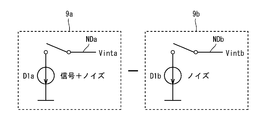
- FIG. 5 is a diagram showing a schematic configuration of the sensor pixel circuit 9.
- the first sensor pixel circuit 9a includes one photodiode D1a and one storage node NDa.
- the photodiode D1a extracts charges from the storage node NDa according to the amount of light (signal + noise) incident while the backlight 3 is lit.
- the second sensor pixel circuit 9b includes one photodiode D1b and one storage node NDb.
- the photodiode D1b extracts charges from the storage node NDb according to the amount of light (noise) incident while the backlight 3 is turned off.
- a sensor signal corresponding to the amount of light incident during the detection period when the backlight 3 is lit is read out.
- a sensor signal corresponding to the amount of light incident during the detection period when the backlight 3 is turned off is read out.
- the difference circuit included in the source driver circuit 6 the difference between the output signal of the first sensor pixel circuit 9 a and the output signal of the second sensor pixel circuit 9 b is obtained, so that the light amount when the backlight is turned on And the difference in the amount of light when the backlight is turned off.
- the number of sensor pixel circuits 9 provided in the pixel region 4 may be arbitrary. However, it is preferable to connect the first sensor pixel circuit 9a and the second sensor pixel circuit 9b to different output lines. For example, when (n ⁇ m) sensor pixel circuits 9 are provided in the pixel region 4, n first sensor pixel circuits 9a are connected to the odd-numbered output lines OUT1 to OUTm-1, respectively, It is only necessary to connect n second sensor pixel circuits 9b to the respective output lines OUT2 to OUTm. In this case, reading from the sensor pixel circuit 9 is performed for each row.
- the same number of sensor pixel circuits 9 as the color pixels may be provided in the pixel region 4.
- a smaller number of sensor pixel circuits 9 than the color pixels may be provided in the pixel region 4.
- the display device is a display device in which a plurality of photodiodes (photosensors) are arranged in the pixel region 4, and includes a plurality of display pixel circuits 8 and a plurality of sensor pixel circuits 9.
- a sensor row driver circuit 7 (drive circuit) that outputs a clock signal CLK (control signal) indicating a detection period when the backlight is turned on and a detection period when the backlight is turned off to the display panel 2 and the sensor pixel circuit 9.
- CLK clock signal
- the sensor pixel circuit is abbreviated as a pixel circuit, and the same name as the signal line is used to identify a signal on the signal line (for example, a signal on the clock line CLKa is referred to as a clock signal CLKa).
- the first sensor pixel circuit 9a is connected to the clock line CLKa, the reset line RSTa, the readout line RWSa, the power supply line VDDa, and the output line OUTa.
- the second sensor pixel circuit 9b is connected to the clock line CLKb, the reset line RSTb, the readout line RWSb, the power supply line VDDb, and the output line OUTb.
- the second sensor pixel circuit 9b has the same configuration as that of the first sensor pixel circuit 9a and operates in the same manner, and thus the description regarding the second sensor pixel circuit 9b is omitted as appropriate.
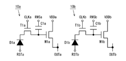
- FIG. 6 is a circuit diagram showing an example of a specific configuration of the first sensor pixel circuit 9a and the second sensor pixel circuit 9b.
- the first pixel circuit 10a shown in FIG. 6 is a specific example of the first sensor pixel circuit 9a
- the second pixel circuit 10b is a specific example of the second sensor pixel circuit 9b.
- the first pixel circuit 10a includes transistors T1a and M1a, a photodiode D1a, and a capacitor C1a.
- the second pixel circuit 10b includes transistors T1b and M1b, a photodiode D1b, and a capacitor C1b.
- the transistors T1a, M1a, T1b, and M1b are N-type TFTs (Thin Film Transistor).
- the anode of the photodiode D1a is connected to the reset line RSTa, and the cathode is connected to the source of the transistor T1a.
- the gate of the transistor T1a is connected to the clock line CLKa, and the drain is connected to the gate of the transistor M1a.
- the drain of the transistor M1a is connected to the power supply line VDDa, and the source is connected to the output line OUTa.
- the capacitor C1a is provided between the gate of the transistor M1a and the read line RWSa.
- a node connected to the gate of the transistor M1a serves as an accumulation node for accumulating charges according to the detected light amount, and the transistor M1a functions as a readout transistor.
- the second pixel circuit 10b has the same configuration as the first pixel circuit 10a.
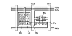
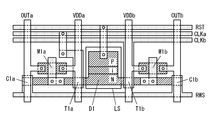
- FIG. 7 is a layout diagram of the first pixel circuit 10a.
- a light shielding film LS As shown in FIG. 7, in the first pixel circuit 10a, a light shielding film LS, a semiconductor layer (shaded portion), a gate wiring layer (dot pattern portion), and a source wiring layer (white coating portion) are sequentially formed on a glass substrate. It is constituted by.
- a contact (indicated by a white circle) is provided at a location where the semiconductor layer and the source wiring layer are connected and a location where the gate wiring layer and the source wiring layer are connected.
- the transistors T1a and M1a are formed by arranging a semiconductor layer and a gate wiring layer so as to cross each other.
- the photodiode D1a is formed by arranging the P layer, I layer, and N semiconductor layers side by side.
- the capacitor C1a is formed by arranging the semiconductor layer and the gate wiring layer so as to overlap each other.
- the light shielding film LS is made of metal, and prevents light entering from the back side of the substrate from entering the photodiode D1a.
- the second pixel circuit 10b is laid out in the same form as the first pixel circuit 10a.
- the first and second pixel circuits 10a and 10b may be laid out in a form other than the above.
- FIG. 8 is a diagram showing the operation of the first pixel circuit 10a when driven by the signal shown in FIG. As shown in FIG. 8, the first pixel circuit 10a performs (a) reset, (b) accumulation, (c) holding, and (d) reading in one frame period.
- FIG. 9 is a signal waveform diagram of the first pixel circuit 10a and the second pixel circuit 10b when driven by the signal shown in FIG.
- BL represents the luminance of the backlight 3
- Vinta represents the potential of the storage node of the first pixel circuit 10a (gate potential of the transistor M1a)
- Vintb represents the potential of the storage node of the second pixel circuit 10b (transistor).
- M1b gate potential).
- the reset period is from time t1 to time t2
- the storage period is from time t2 to time t3
- the holding period is from time t3 to time t7
- the readout period is from time t7 to time t8.
- the time t4 to time t5 is the reset period
- the time t5 to time t6 is the accumulation period
- the time t6 to time t7 is the holding period
- the time t7 to time t8 is the reading period.
- the clock signal CLKa is at a high level
- the readout signal RWSa is at a low level
- the reset signal RSTa is at a reset high level.
- the transistor T1a is turned on. Therefore, a current (forward current of the photodiode D1a) flows from the reset line RSTa to the storage node via the photodiode D1a and the transistor T1a (FIG. 8A), and the potential Vanta is reset to a predetermined level.
- the clock signal CLKa is at a high level, and the reset signal RSTa and the readout signal RWSa are at a low level.
- the transistor T1a is turned on.
- a current photocurrent of the photodiode D1a
- the potential Vanta falls according to the amount of light incident during the period in which the clock signal CLKa is at the high level (lighting period of the backlight 3).
- the clock signal CLKa, the reset signal RSTa, and the readout signal RWSa are at a low level.
- the transistor T1a is turned off.
- the transistor T1a is off and the gate of the photodiode D1a and the transistor M1 is electrically cut off, so that the potential Vanta does not change (FIG. 8). (C)).
- the clock signal CLKa and the reset signal RSTa are at a low level, and the readout signal RWSa is at a readout high level.
- the transistor T1a is turned off.
- the potential Vanta increases by (Cqa / Cpa) times the increase amount of the potential of the readout signal RWSa (where Cpa is the overall capacitance value of the first pixel circuit 10a and Cqa is the capacitance value of the capacitor C1a).
- the transistor M1a forms a source follower amplifier circuit using a transistor (not shown) included in the source driver circuit 6 as a load, and drives the output line OUTa according to the potential Vanta (FIG. 8D).
- the second pixel circuit 10b operates in the same manner as the first pixel circuit 10a.
- the potential Vintb is reset to a predetermined level during the reset period, falls during the accumulation period according to the amount of light incident during the period when the clock signal CLKb is at the high level (backlight extinguishing period), and does not change during the holding period. .
- the potential Vintb increases by (Cqb / Cpb) times the amount of increase in the potential of the readout signal RWSb (where Cpb is the overall capacitance value of the second pixel circuit 10b, and Cqb is the capacitance value of the capacitor C1b).
- the transistor M1b drives the output line OUTb according to the potential Vintb.
- the first pixel circuit 10a includes one photodiode D1a (photosensor), one accumulation node that accumulates charges according to the detected light amount, and an accumulation node. It includes a transistor M1a (readout transistor) having a connected control terminal, and a transistor T1a (holding switching element) provided on the path of a current flowing through the photodiode D1a and turned on / off in accordance with the clock signal CLK.
- the transistor T1a is provided between the storage node and one end of the photodiode D1a, and the other end of the photodiode D1a is connected to the reset line RSTa.
- the transistor T1a is turned on in the detection period when the backlight is lit in accordance with the clock signal CLKa.
- the second pixel circuit 10b has the same configuration as the first pixel circuit 10a, and the transistor T1b included in the second pixel circuit 10b is turned on in the detection period when the backlight is turned off.
- the transistor T1a that is turned on in the detection period when the backlight is turned on is provided on the path of the current that flows through the photodiode D1a, and the transistor T1b that is turned on in the detection period when the backlight is turned off on the path of the current that flows through the photodiode D1b. Is provided.
- the light is detected in the detection period when the backlight is turned on, and the light is detected in the detection period when the backlight is extinguished, and the first pixel circuit 10a that holds the detected light amount in other cases.
- the second pixel circuit 10b that holds the amount of light can be configured.
- the first and second pixel circuits 10a and 10b further include capacitors C1a and C1b provided between the storage node and the read lines RWSa and RWSb, respectively. Therefore, by applying a read potential to the read lines RWSa and RWSb, the potential of the storage node can be changed, and a signal corresponding to the detected light amount can be read from the first and second pixel circuits 10a and 10b.
- the display panel 2 further includes a plurality of output lines OUT1 to OUTm that propagate the output signals of the first and second pixel circuits 10a and 10b, and the first pixel circuit 10a and the second pixel circuit 10b have different outputs for each type. Connected to the wire. Therefore, reading from the first and second pixel circuits 10a and 10b can be performed in parallel, the reading speed can be reduced, and the power consumption of the apparatus can be reduced.
- the display device corrects offset errors of the first pixel circuit 10a and the second pixel circuit 10b in addition to the sensor drive mode described with reference to FIGS. 4 and 9 above.
- These two types of correction data acquisition modes are provided as operation modes.
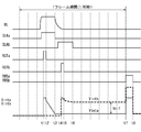
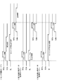
- FIG. 10 is a timing chart showing drive signals in the sensor drive mode, drive signals in the first correction data acquisition mode, and drive signals in the second correction data acquisition mode.
- the time point and length of the reset signal at a high level within one frame period are The same.
- the length of the clock signal is different from the length of the lighting period of the sensing backlight.
- the sensor signals are read from the first and second pixel circuits 10a and 10b in the sensor drive mode, and at the predetermined timing, the first signal shown in FIG.
- correction data is acquired. That is, in the display device according to the present embodiment, a frame that operates in the first correction data acquisition mode and a frame that operates in the second correction data acquisition mode between one or a plurality of frames in the sensor drive mode. are provided as appropriate.
- the frequency of the frame operating in the first correction data acquisition mode and the frame operating in the second correction data acquisition mode is arbitrary.
- the frame for the first correction data acquisition mode and the frame for the second correction data acquisition mode may be continuous, or one or more frames depending on the sensor drive mode may be interposed therebetween. Further, a frame for the second correction data acquisition mode may be arranged before the frame for the first correction data acquisition mode.
- an output corresponding to the potential Vinta is obtained from the first pixel circuit 10a
- an output corresponding to the potential Vintb is obtained from the second pixel circuit 10b.
- first correction data B 1st for correcting the offset of the first pixel circuit 10a in the sensor drive mode is obtained from the first pixel circuit 10a in the readout period.
- second correction data B 2nd for correcting the offset of the second pixel circuit 10b in the sensor driving mode is obtained from the second pixel circuit 10b in the readout period.
- the timings at which the clock signals CLKa and CLKb rise are the same in one frame period for all of the sensor drive mode, the first correction data acquisition mode, and the second correction data acquisition mode.
- the length of the period in which the clock signal CLKa is at the high level is equal to the length of the period in which the clock signal CLKb is at the high level.
- the length of the period in which the clock signal CLKa is at the high level in the first correction data acquisition mode and the second correction data acquisition mode is greater than the length of the period in which the clock signal CLKa is at the high level in the sensor drive mode. Also short. In other words, the length of the accumulation period in the first correction data acquisition mode and the second correction data acquisition mode is shorter than the length of the accumulation period in the sensor drive mode.
- the length of the accumulation period in the first correction data acquisition mode and the second correction data acquisition mode is substantially zero so as not to be affected by the photocurrent due to external light or the like.
- the clock signal CLKa may be switched from the high level to the low level after the reset signal RSTa is switched from the high level to the low level.
- the length of the accumulation period is such that the order of falling of the reset signal RSTa (switching from high level to low level) and falling of the clock signal CLKa is not reversed due to variations in signal timing.
- the length of the predetermined margin period is sufficient.
- the accumulation period in this case is preferably a short time of about several microseconds depending on the design.
- the RST signal RSTa may fall after the fall of the clock signal CLKa in the first correction data acquisition mode and the second correction data acquisition mode. In this case, the length of the accumulation period is effectively zero.
- the sensing backlight starts lighting in synchronization with the rising edge of the clock signal CLKa in all modes.
- the present invention is not limited to this, and the rising edge of the clock signal CLKa may be after or before the start of lighting of the backlight.
- the length of the period from the start of lighting of the backlight to the rise of the clock signal CLKa is equal.
- the length of the backlight lighting period is equal in the case of the sensor drive mode and the case of the second correction data acquisition mode.
- the length of the backlight lighting period in the first correction data acquisition mode is shorter than the backlight lighting period in the sensor drive mode and the second correction data acquisition mode.
- the length of the period from the end of the accumulation period to the backlight turn-off in the first correction data acquisition mode is shorter than the period from the end of the accumulation period to the backlight turn-off in the sensor drive mode.
- the backlight is turned off when a predetermined time elapses after the clock signal CLKa falls (that is, after the accumulation period ends). Also in the first correction data acquisition mode, it is preferable that the backlight is turned off when the same time as the predetermined time has elapsed after the fall of the clock signal CLKa.
- the first correction data B 1st for correcting the offset of the first pixel circuit 10a in the sensor drive mode is obtained from the first pixel circuit 10a.
- second correction data B 2nd for correcting the offset of the second pixel circuit 10b in the sensor drive mode is obtained from the second pixel circuit 10b.
- the charge accumulation state in the accumulation period within the backlight lighting period is affected by the length of the backlight lighting period before the reset period.
- the length of the backlight lighting period before the reset period is set equal in both the sensor drive mode and the first correction data acquisition mode. Therefore, in the case of the sensor drive mode and the case of the first correction data acquisition mode, the influence of the length of the backlight lighting period before the reset period can be made the same condition.
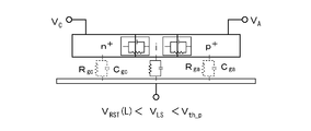
- FIG. 12 is a schematic cross-sectional view of the diode D1a.
- the diode is divided into three by the parasitic capacitance generated between the light shielding film LS.
- the potential V LS of the gate that is, the light shielding film LS, the anode potential V A, and the cathode potential V C.
- the distribution of the modes A, B, and C is represented by the relationship between the anode potential V A and the potential V LS of the light shielding film LS as shown in FIG.
- an area without hatching is mode A
- an area with lower right hatching is mode B
- an area with lower left hatching is mode C.
- t0 is a coordinate representing V LS and V A when the reset signal RSTa becomes high level.
- t1 corresponds to the time when the reset signal RSTa switches from the high level to the low level, and t2 corresponds to the time when the clock signal CLKa switches from the high level to the low level.
- the diode D1a is in the mode B state at the time when the reset signal RSTa becomes high level (at the start of reset, ie, time t0).
- the diode D1a When in the mode B state, the diode D1a is in a state where holes are accumulated in the i layer, as shown in FIG. 14A.
- the diode D1a At the time when the reset signal RSTa is switched to the low level (that is, time t1), the diode D1a is in the mode A state, and as shown in FIG. 14B, holes are trapped in the i layer. Therefore, in the reset period, the diode D1a is in the mode B state shown in FIG. 14A, and is affected by light from the backlight immediately before the reset period.
- the reset level and the reset field through amount of the diode D1a depend on the lighting condition of the backlight immediately before the reset period.
- the length of the backlight lighting period before the reset period is set to be equal to each other. Yes.
- the first correction data acquisition mode allows the first pixel circuit 10a in the sensor drive mode.
- First correction data B 1st for correcting the offset is obtained.
- the period from the end of the accumulation period to the backlight turn-off is set to be equal in the sensor drive mode and in the first correction data acquisition mode. This is because the influence of the leakage of the transistor T1a due to the light from the backlight entering the diode D1a during the period from the end of the accumulation period to the backlight extinction is obtained in the sensor driving mode and the first correction data acquisition. This is to make it uniform in the mode. That is, even after the clock signal CLKa becomes low level and the accumulation period ends, while the backlight is lit, light from the backlight passes through the light-shielding film LS or the configuration in the panel. There is a light component that is reflected by the member and incident on the transistor T1a.
- second correction data B 2nd for correcting the offset of the second pixel circuit 10b in the sensor drive mode is obtained as the output of the second pixel circuit 10b.
- the backlight lighting period in one frame period has the same timing and the same length as the lighting period in the sensor drive mode. is there. Accordingly, the lighting condition of the backlight immediately before the reset period of the second pixel circuit 10b (the period in which the reset signal RSTb is high level) is the same as that in the sensor drive mode.
- the second level in the sensor driving mode is obtained under the condition that the reset level and the reset field through amount of the diode D1b are the same as those in the sensor driving mode.
- Second correction data B 2nd for correcting the offset of the pixel circuit 10b can be obtained.
- the signal processing circuit 20 corrects the sensor output obtained in the sensor drive mode using the first correction data B 1st and the second correction data B 2nd obtained as described above.
- a specific example of the correction process will be described below.
- the following correction processing is performed by the signal processing circuit 20, but it may be configured to be performed by an arithmetic circuit provided in the source driver circuit 6. [Specific example 1 of correction]
- the gain correction optical sensor signal level W 1st is obtained by supplying a read pulse whose amplitude is smaller than that in the sensor drive mode (the amplitude may be zero).
- the gain correction optical sensor signal level W 2nd is acquired by supplying a read pulse having an amplitude smaller than that in the sensor drive mode (the amplitude may be zero).
- the optical sensor signal level B obtained from the second pixel circuit 10b by the sensor driving mode, the gain correcting optical sensor signal level W 1st and the gain correcting optical sensor signal level W 2nd , From the photosensor signal level R obtained from the first pixel circuit 10a in the sensor driving mode using the tone number L of the photosensor signal, the corrected photosensor signal level R ′ is R ′ L ⁇ ⁇ (R ⁇ B 1st ) / (W 1st ⁇ B 1st ) ⁇ (B ⁇ B 2nd ) / (W 2nd ⁇ B 2nd ) ⁇ Ask for.
- FIG. 15 is a circuit diagram of a pixel circuit according to the second embodiment of the present invention.
- a pixel circuit 30 shown in FIG. 15 includes transistors T1a, T1b, M1a, M1b, a photodiode D1, and capacitors C1a, C1b.
- the transistors T1a, T1b, M1a, and M1b are N-type TFTs.
- the left half corresponds to the first pixel circuit
- the right half corresponds to the second pixel circuit.
- the pixel circuit 30 is connected to clock lines CLKa and CLKb, a reset line RST, a readout line RWS, power supply lines VDDa and VDDb, and output lines OUTa and OUTb.
- the anode of the photodiode D1 is connected to the reset line RST, and the cathode is connected to the sources of the transistors T1a and T1b.
- the gate of the transistor T1a is connected to the clock line CLKa, and the drain is connected to the gate of the transistor M1a.
- the drain of the transistor M1a is connected to the power supply line VDDa, and the source is connected to the output line OUTa.
- the capacitor C1a is provided between the gate of the transistor M1a and the read line RWS.
- the gate of the transistor T1b is connected to the clock line CLKb, and the drain is connected to the gate of the transistor M1b.
- the drain of the transistor M1b is connected to the power supply line VDDb, and the source is connected to the output line OUTb.
- the capacitor C1b is provided between the gate of the transistor M1b and the read line RWS.
- a node connected to the gate of the transistor M1a is a first storage node
- a node connected to the gate of the transistor M1b is a second storage node
- the transistors M1a and M1b function as readout transistors.
- FIG. 16 is a layout diagram of the pixel circuit 30. The description of FIG. 16 is the same as that of the first embodiment.
- FIG. 17 is a diagram illustrating the operation of the pixel circuit 30 in the sensor driving mode.
- the pixel circuit 30 includes (a) reset when the backlight is turned on, (b) accumulation when the backlight is turned on, (c) reset when the backlight is turned off, and (d) turn off the backlight in one frame period. Accumulation of time, (e) holding, and (f) reading are performed.
- FIG. 18 is a signal waveform diagram of the pixel circuit 30 in the sensor driving mode.
- Vanta represents the potential of the first storage node (the gate potential of the transistor M1a)
- Vintb represents the potential of the second storage node (the gate potential of the transistor M1b).
- time t1 to time t2 is a reset period when the backlight is turned on
- time t2 to time t3 is an accumulation period when the backlight is turned on
- time t4 to time t5 is a reset period when the backlight is turned off
- time t5 to time t6 is an accumulation period when the backlight is extinguished
- time t3 to time t4 and time t6 to time t7 are holding periods
- time t7 to time t8 are reading periods.
- the clock signal CLKa is at a high level
- the clock signal CLKb and the readout signal RWS are at a low level
- the reset signal RST is at a high level for reset.
- the transistor T1a is turned on and the transistor T1b is turned off. Therefore, a current (forward current of the photodiode D1) flows from the reset line RST to the first accumulation node via the photodiode D1 and the transistor T1a (FIG. 17A), and the potential Vanta is reset to a predetermined level. .
- the clock signal CLKa is at a high level
- the clock signal CLKb, the reset signal RST, and the readout signal RWS are at a low level.
- the transistor T1a is turned on and the transistor T1b is turned off.
- a current photocurrent of the photodiode D1 flows from the first storage node to the reset line RST via the transistor T1a and the photodiode D1, and the charge is transferred from the first storage node. It is pulled out (FIG. 17 (b)). Therefore, the potential Vanta falls according to the amount of light incident during this period (lighting time of the backlight 3). Note that the potential Vintb does not change during this period.
- the clock signal CLKb is at a high level
- the clock signal CLKa and the read signal RWS are at a low level
- the reset signal RST is at a high level for reset.
- the transistor T1a is turned off and the transistor T1b is turned on. Therefore, a current (forward current of the photodiode D1) flows from the reset line RST to the second accumulation node via the photodiode D1 and the transistor T1b (FIG. 17C), and the potential Vintb is reset to a predetermined level. .
- the clock signal CLKb is at a high level, and the clock signal CLKa, the reset signal RST, and the read signal RWS are at a low level.
- the transistor T1a is turned off and the transistor T1b is turned on.
- a current photocurrent of the photodiode D1 flows from the second storage node to the reset line RST via the transistor T1b and the photodiode D1, and the charge is transferred from the second storage node. It is pulled out (FIG. 17 (d)). Therefore, the potential Vintb drops according to the amount of light incident during this period (backlight 3 extinguishing time). Note that the potential Vanta does not change during this period.
- the clock signals CLKa and CLKb, the reset signal RST, and the read signal RWS are at a low level.
- the transistors T1a and T1b are turned off. Even if light is incident on the photodiode D1 at this time, the transistors T1a and T1b are turned off, and the gates of the photodiode D1 and the transistors M1a and M1b are electrically disconnected. Therefore, the potentials Vinta and Vintb Does not change (FIG. 17E).
- the clock signals CLKa and CLKb and the reset signal RST are at a low level, and the read signal RWS is at a high level for reading.
- the transistors T1a and T1b are turned off.
- the potentials Vinta and Vintb increase by the increase in the potential of the read signal RWS, a current Ia corresponding to the potential Vinta flows between the drain and source of the transistor M1a, and the potential between the drain and source of the transistor M1b.
- An amount of current Ib corresponding to Vintb flows (FIG. 17 (f)).
- the current Ia is input to the source driver circuit 6 via the output line OUTa
- the current Ib is input to the source driver circuit 6 via the output line OUTb.
- the pixel circuit 30 has a configuration in which one photodiode D1 (photosensor) is shared between the first and second pixel circuits 10a and 10b according to the first embodiment.
- the cathode of the shared photodiode D1 is connected to the source of the transistor T1a included in the portion corresponding to the first pixel circuit and the source of the transistor T1b included in the portion corresponding to the second pixel circuit.
- the pixel circuit 30 as in the first and second pixel circuits 10a and 10b according to the first embodiment, it is possible to detect the light amount when the backlight is turned on and the light amount when the backlight is turned off. Thereby, the effect similar to 1st Embodiment is acquired. Further, by sharing one photodiode D1 between the two types of pixel circuits, there is no difference in the characteristics of the photodiodes between the two types of pixel circuits. Thereby, the difference between the light amount when the backlight is turned on and the light amount when the backlight is turned off can be accurately obtained. In addition, the number of photodiodes can be reduced, the aperture ratio can be increased, and the sensitivity of the sensor pixel circuit can be increased.
- the frames for the first correction data acquisition mode and the second correction data acquisition mode are appropriately inserted between the frames for the sensor drive mode. Then, it is possible to correct at least one of the offset and gain of the sensor output obtained in the sensor drive mode using the first correction data B 1st and the second correction data B 2nd obtained in these modes. Thereby, as in the first embodiment, a sensor output with high accuracy and a wide dynamic range can be obtained.
- 19A to 19E are circuit diagrams of pixel circuits according to first to fifth modifications of the first embodiment, respectively.
- the first pixel circuits 11a to 17a shown in FIGS. 19A to 19E are obtained by making the following modifications to the first pixel circuit 10a according to the first embodiment.
- the second pixel circuits 11b to 17b are obtained by performing the same modification on the second pixel circuit 10b according to the first embodiment.
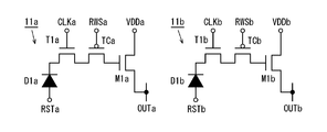
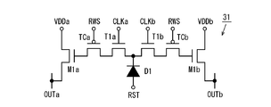
- the first pixel circuit 11a shown in FIG. 19A is obtained by replacing the capacitor C1 included in the first pixel circuit 10a with a transistor TCa that is a P-type TFT.
- the drain of the transistor TCa is connected to the drain of the transistor T1a
- the source is connected to the gate of the transistor M1a
- the gate is connected to the readout line RWSa.
- the transistor TCa connected in this way changes the potential of the storage node more than the original pixel circuit when a high level for reading is applied to the reading line RWSa.
- the difference between the potential of the storage node when the strong light is incident and the potential of the storage node when the weak light is incident can be amplified to improve the sensitivity of the pixel circuit 11a.
- the pixel circuit 31 shown in FIG. 24A is obtained.
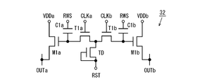
- the first pixel circuit 12a shown in FIG. 19B is obtained by replacing the photodiode D1 included in the first pixel circuit 10a with a phototransistor TDa. Thereby, all the transistors included in the first pixel circuit 12a are N-type. Therefore, the first pixel circuit 12a can be manufactured using a single channel process that can manufacture only N-type transistors. When the same modification is performed on the second embodiment, a pixel circuit 32 shown in FIG. 24B is obtained.
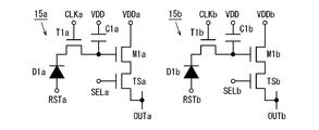
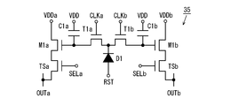
- a first pixel circuit 15a shown in FIG. 19C is obtained by adding a transistor TSa to the first pixel circuit 10a.
- the transistor TSa is an N-type TFT and functions as a selection switching element.
- the source of the transistor M1a is connected to the drain of the transistor TSa.
- the source of the transistor TSa is connected to the output line OUTa, and the gate is connected to the selection line SELa.
- the selection signal SELa is at a high level when reading from the first pixel circuit 15a.
- the capacitor C1a is connected to the readout line RSWa in the first pixel circuit 10a, but is connected to the power supply line VDD in the first pixel circuit 15a. Thereby, variations of the pixel circuit can be obtained.
- a pixel circuit 35 shown in FIG. 24C is obtained.
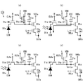
- FIG. 20 is a diagram illustrating the operation of the first pixel circuit 15a in the sensor drive mode.
- FIG. 21 is a signal waveform diagram of the first pixel circuit 15a.
- the selection signal SELa is at a low level, the transistor TSa is turned off, and the first pixel circuit 15a operates in the same manner as the first pixel circuit 10a (FIGS. 20A to 20C).
- the selection signal SELa becomes high level and the transistor TSa is turned on.
- an amount of current Ia corresponding to the potential Vanta flows between the drain and source of the transistor M1a (FIG. 20D).
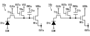
- the first pixel circuit 16a shown in FIG. 19D is obtained by adding a transistor TRa to the first pixel circuit 10a.
- the transistor TRa is an N-type TFT and functions as a reset switching element.
- the low-level potential VSS is applied to the source of the transistor TRa, the drain is connected to the gate of the transistor M1a, and the gate is connected to the reset line RSTa.
- the low level potential COM is applied to the anode of the photodiode D1a.
- a pixel circuit 36 shown in FIG. 24D is obtained.
- FIG. 22 is a diagram illustrating the operation of the first pixel circuit 16a in the sensor drive mode.
- the reset signal RSTa becomes high level, the transistor TRa is turned on, and the potential of the storage node (gate potential of the transistor M1a) is reset to the low level potential VSS (FIG. 22A).
- the reset signal RSTa goes low, and the transistor TRb is turned off (FIGS. 22B to 22D).
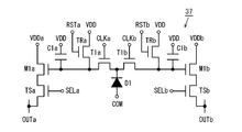
- a first pixel circuit 17a shown in FIG. 19E is obtained by adding the transistors TSa and TRa to the first pixel circuit 10a.
- the connection form of the transistors TSa and TRa is the same as that of the first pixel circuits 15a and 16a. Thereby, variations of the pixel circuit can be obtained.
- a pixel circuit 37 shown in FIG. 24E is obtained.
- FIG. 23 is a diagram illustrating the operation of the first pixel circuit 17a in the sensor drive mode.
- the reset signal RSTa becomes high level
- the transistor TRa is turned on
- the potential of the storage node (gate potential of the transistor M1a) is reset to the high level potential VDD (FIG. 23 (a)).
- the selection signal SELa becomes high level and the transistor TSa is turned on.
- an amount of current Ia corresponding to the potential Vanta flows between the drain and source of the transistor M1a (FIG. 23 (d)).
- the reset signal RSTa and the selection signal SELa are at a low level (FIGS. 23B and 23C).
- the display device As described above, the display device according to each of the above-described embodiments and the modifications thereof detects the light during the detection period when the backlight is turned on, and holds the detected light amount otherwise.
- a second sensor pixel circuit that detects light during the detection period when the backlight is turned off and holds the detected light quantity is provided separately.
- the display device can obtain the difference between the two kinds of light amounts outside the sensor pixel circuit, and can detect the difference between the light amount when the backlight is turned on and the light amount when the backlight is turned off. Therefore, the conventional problem can be solved and an input function independent of the light environment can be provided.
- the type of light source provided in the display device is not particularly limited. Therefore, for example, a visible light backlight provided for display may be turned on and off. Alternatively, an infrared backlight for light detection may be provided in the display device separately from the visible light backlight for display. In such a display device, the visible light backlight may be always turned on, and only the infrared light backlight may be turned on and off once in one frame period.
Landscapes
- Physics & Mathematics (AREA)
- Engineering & Computer Science (AREA)
- Nonlinear Science (AREA)
- General Physics & Mathematics (AREA)
- Theoretical Computer Science (AREA)
- Mathematical Physics (AREA)
- Chemical & Material Sciences (AREA)
- Crystallography & Structural Chemistry (AREA)
- General Engineering & Computer Science (AREA)
- Optics & Photonics (AREA)
- Human Computer Interaction (AREA)
- Computer Hardware Design (AREA)
- Liquid Crystal (AREA)
- Liquid Crystal Display Device Control (AREA)
- Control Of Indicators Other Than Cathode Ray Tubes (AREA)
Abstract
Description
R’=(R-B1st)-(B-B2nd)
により求めることが好ましい(第8の構成)。
R’=L×{R/(W1st-B1st)-B/(W2nd-B2nd)}
により求めることとしても良い(第9の構成)。
R’=L×{(R-B1st)/(W1st-B1st)-
(B-B2nd)/(W2nd-B2nd)}
により求める構成とすることも好ましい(第10の構成)。
[実施の形態]
[第1の実施形態]
VA+Vth_p≦VLS≦VC+Vth_n
モードBの領域は、
VLS≦VA+Vth_p
モードCの領域は、
VC+Vth_n≦VLS
と表すことができる。
[補正の具体例1]
R’=(R-B1st)-(B-B2nd)
により求める。
[補正の具体例2]
R’=L×{R/(W1st-B1st)-B/(W2nd-B2nd)}
により求める。
[補正の具体例3]
R’=L×{(R-B1st)/(W1st-B1st)-
(B-B2nd)/(W2nd-B2nd)}
により求める。
[第2の実施形態]
[回路構成の変形例]
Claims (14)
- アクティブマトリクス基板を備えた表示装置であって、
前記アクティブマトリクス基板の画素領域に設けられた光センサと、
前記光センサに接続されたセンサ駆動配線と、
前記光センサへ、前記センサ駆動配線を介して、センサ駆動信号を供給するセンサ駆動回路と、
前記センサ駆動信号に従って前記光センサから読み出された信号を増幅し、光センサ信号として出力するアンプ回路と、
前記アンプ回路から出力された光センサ信号を処理する信号処理回路と、
前記光センサ用の光源とを備え、
前記光センサには、
前記センサ駆動信号に従い、前記光源点灯時の蓄積期間で受光量に応じた電荷を蓄積し、読み出し期間が到来すると蓄積電荷に応じたセンサ信号を出力する第1センサ画素回路と、
前記センサ駆動信号に従い、前記光源消灯時の蓄積期間で受光量に応じた電荷を蓄積し、読み出し期間が到来すると蓄積電荷に応じたセンサ信号を出力する第2センサ画素回路とが含まれ、
前記センサ駆動回路が、1フレーム期間の動作モードとして、
前記光センサの前記第1センサ画素回路および前記第2センサ画素回路のそれぞれから前記センサ信号を得るためのセンサ駆動モードと、
前記センサ駆動モードとは異なるセンサ駆動信号を用いて、前記第1センサ画素回路から得られるセンサ信号を補正するための第1の補正用データを取得する第1の補正用データ取得モードと、
前記センサ駆動モードとは異なるセンサ駆動信号を用いて、前記第2センサ画素回路から得られるセンサ信号を補正するための第2の補正用データを取得する第2の補正用データ取得モードとを有し、
前記第1の補正用データ取得モードにおける前記光源点灯時の蓄積期間が、前記センサ駆動モードにおける前記光源点灯時の蓄積期間よりも短く、
前記第2の補正用データ取得モードにおける前記光源消灯時の蓄積期間が、前記センサ駆動モードにおける前記光源消灯時の蓄積期間よりも短い、表示装置。 - 前記第1の補正用データ取得モードにおける前記光源点灯期間が、前記センサ駆動モードにおける前記光源点灯期間より短い、請求項1に記載の表示装置。
- 前記第1の補正用データ取得モードにおいて、1フレーム期間における前記光源点灯開始のタイミングが、前記センサ駆動モードと同じタイミングである、請求項2に記載の表示装置。
- 前記第1の補正用データ取得モードにおける前記蓄積期間の開始時点から前記光源点灯期間の終了時点までの期間が、前記センサ駆動モードにおける前記蓄積期間の開始時点から前記光源点灯期間の終了時点までの期間よりも短い、請求項3に記載の表示装置。
- 前記第1の補正用データ取得モードにおいて、前記蓄積期間の終了時点から前記光源点灯期間の終了時点までの期間の長さが、前記センサ駆動モードにおける前記蓄積期間の終了時点から前記光源点灯期間の終了時点までの期間の長さと等しい、請求項4に記載の表示装置。
- 前記第2の補正用データ取得モードにおける前記光源点灯期間が、前記第1の補正用データ取得モードにおける前記光源点灯期間より長い、請求項1に記載の表示装置。
- 前記第2の補正用データ取得モードにおいて、1フレーム期間における前記光源点灯期間の開始および終了のタイミングが、前記センサ駆動モードの場合の1フレーム期間における前記光源点灯期間の開始および終了のタイミングと等しい、請求項6に記載の表示装置。
- 前記センサ駆動モードにより前記第2センサ画素回路から得られる光センサ信号レベルをBと表記し、前記第1の補正用データ取得モードにより前記第1センサ画素回路から得られる光センサ信号レベルをB1stと表記し、前記第2の補正用データ取得モードにより前記第1センサ画素回路から得られる光センサ信号レベルをB2ndと表記した場合、
前記信号処理回路が、前記センサ駆動モードにより前記第1センサ画素回路から得られる光センサ信号レベルRから、補正後の光センサ信号レベルR’を、
R’=(R-B1st)-(B-B2nd)
により求める、請求項1~7のいずれか一項に記載の表示装置。 - 前記第1の補正用データ取得モードにおいて、前記センサ駆動回路が、センサ駆動モード時の読み出し信号の振幅よりも小さい振幅を有する読み出し信号を供給することにより、ゲイン補正用光センサ信号レベルW1stを取得し、
前記第2の補正用データ取得モードにおいて、前記センサ駆動回路が、センサ駆動モード時の読み出し信号の振幅よりも小さい振幅を有する読み出し信号を供給することにより、ゲイン補正用光センサ信号レベルW2ndを取得し、
光センサ信号の階調数をLと表記した場合、
前記信号処理回路が、前記センサ駆動モードにより前記第1センサ画素回路から得られる光センサ信号レベルRから、補正後の光センサ信号レベルR’を
R’=L×{R/(W1st-B1st)-B/(W2nd-B2nd)}
により求める、請求項1~7のいずれか一項に記載の表示装置。 - 前記センサ駆動モードにより前記第2センサ画素回路から得られる光センサ信号レベルをBと表記し、前記第1の補正用データ取得モードにより前記第1センサ画素回路から得られる光センサ信号レベルをB1stと表記し、前記第2の補正用データ取得モードにより前記第1センサ画素回路から得られる光センサ信号レベルをB2ndと表記し、
前記第1の補正用データ取得モードにおいて、前記センサ駆動回路が、センサ駆動モード時の読み出し信号の振幅よりも小さい振幅を有する読み出し信号を供給することにより、ゲイン補正用光センサ信号レベルW1stを取得し、
前記第2の補正用データ取得モードにおいて、前記センサ駆動回路が、センサ駆動モード時の読み出し信号の振幅よりも小さい振幅を有する読み出し信号を供給することにより、ゲイン補正用光センサ信号レベルW2ndを取得し、
光センサ信号の階調数をLと表記した場合、
前記信号処理回路が、前記センサ駆動モードにより前記第1センサ画素回路から得られる光センサ信号レベルRから、補正後の光センサ信号レベルR’を、
R’=L×{(R-B1st)/(W1st-B1st)-
(B-B2nd)/(W2nd-B2nd)}
により求める、請求項1~7のいずれか一項に記載の表示装置。 - 前記第1および第2センサ画素回路は、
1個の受光素子と、
検知した光量に応じた電荷を蓄積する1個の蓄積ノードと、
前記蓄積ノードに電気的に接続可能な制御端子を有する読み出しトランジスタと、
前記受光素子を流れる電流の経路上に設けられ、前記制御信号に従いオン/オフする保持用スイッチング素子とを含む、請求項1~10のいずれか一項に記載の表示装置。 - 前記第1および第2センサ画素回路において、
前記保持用スイッチング素子は、前記蓄積ノードと前記受光素子の一端との間に設けられ、
前記受光素子の他端はリセット線に接続されている、請求項11に記載の表示装置。 - 前記第1および第2センサ画素回路は、1個の受光素子を共有し、
前記受光素子の一端は前記第1および第2センサ画素回路にそれぞれ含まれる保持用スイッチング素子の一端に接続され、他端は前記リセット線に接続されている、請求項1~10のいずれか一項に記載の表示装置。 - 前記アクティブマトリクス基板に対向する対向基板と、
前記アクティブマトリクス基板と対向基板との間に挟持された液晶とをさらに備えた、請求項1~13のいずれか一項に記載の表示装置。
Priority Applications (3)
| Application Number | Priority Date | Filing Date | Title |
|---|---|---|---|
| EP11783610.6A EP2573754A4 (en) | 2010-05-20 | 2011-05-19 | DISPLAY DEVICE WITH TOUCH SENSOR |
| CN201180025042.5A CN102906807B (zh) | 2010-05-20 | 2011-05-19 | 带有触摸传感器的显示装置 |
| US13/698,745 US9064460B2 (en) | 2010-05-20 | 2011-05-19 | Display device with touch sensor including photosensor |
Applications Claiming Priority (2)
| Application Number | Priority Date | Filing Date | Title |
|---|---|---|---|
| JP2010-116413 | 2010-05-20 | ||
| JP2010116413 | 2010-05-20 |
Publications (1)
| Publication Number | Publication Date |
|---|---|
| WO2011145676A1 true WO2011145676A1 (ja) | 2011-11-24 |
Family
ID=44991768
Family Applications (1)
| Application Number | Title | Priority Date | Filing Date |
|---|---|---|---|
| PCT/JP2011/061497 Ceased WO2011145676A1 (ja) | 2010-05-20 | 2011-05-19 | タッチセンサ付き表示装置 |
Country Status (4)
| Country | Link |
|---|---|
| US (1) | US9064460B2 (ja) |
| EP (1) | EP2573754A4 (ja) |
| CN (1) | CN102906807B (ja) |
| WO (1) | WO2011145676A1 (ja) |
Families Citing this family (11)
| Publication number | Priority date | Publication date | Assignee | Title |
|---|---|---|---|---|
| WO2011145677A1 (ja) * | 2010-05-20 | 2011-11-24 | シャープ株式会社 | タッチセンサ付き表示装置 |
| US20130063407A1 (en) * | 2010-05-20 | 2013-03-14 | Sharp Kabushiki Kaisha | Display device |
| KR102043165B1 (ko) * | 2013-01-30 | 2019-11-12 | 삼성디스플레이 주식회사 | 표시 장치 |
| GB201305288D0 (en) * | 2013-03-22 | 2013-05-01 | St Microelectronics Res & Dev | A sensor and input device such as a touch screen including such a sensor, display device and method |
| CN103413522B (zh) * | 2013-07-31 | 2015-04-22 | 京东方科技集团股份有限公司 | 一种像素电路、有机电致发光显示面板及显示装置 |
| CN103413521B (zh) * | 2013-07-31 | 2015-06-10 | 京东方科技集团股份有限公司 | 有机发光二极管像素电路及其驱动方法、显示装置 |
| US9330604B2 (en) | 2013-07-31 | 2016-05-03 | Boe Technology Group Co., Ltd. | Organic light-emitting diode pixel circuit, drive method thereof, and display device |
| CN109923605B (zh) * | 2016-11-11 | 2021-05-11 | 夏普株式会社 | 带触摸传感器的显示装置及其驱动方法 |
| TWI658393B (zh) * | 2017-12-19 | 2019-05-01 | 友達光電股份有限公司 | 光學觸控系統 |
| US11302102B2 (en) * | 2020-01-22 | 2022-04-12 | Novatek Microelectronics Corp. | Method for controlling display panel and control circuit using the same |
| JP7411474B2 (ja) * | 2020-03-27 | 2024-01-11 | 株式会社ジャパンディスプレイ | 検出装置、指紋検出装置及び静脈検出装置 |
Citations (4)
| Publication number | Priority date | Publication date | Assignee | Title |
|---|---|---|---|---|
| JPH0472732B2 (ja) | 1985-01-14 | 1992-11-19 | Yanmar Diesel Engine Co | |
| JP3521187B2 (ja) | 1996-10-18 | 2004-04-19 | 株式会社東芝 | 固体撮像装置 |
| JP2008096928A (ja) * | 2006-10-16 | 2008-04-24 | Toshiba Matsushita Display Technology Co Ltd | 液晶表示装置、液晶表示装置の駆動方法、プログラム、及び記録媒体 |
| JP2008202828A (ja) * | 2007-02-19 | 2008-09-04 | Daikin Ind Ltd | 操作装置 |
Family Cites Families (10)
| Publication number | Priority date | Publication date | Assignee | Title |
|---|---|---|---|---|
| JP4065671B2 (ja) * | 2001-08-31 | 2008-03-26 | シャープ株式会社 | 不揮発性半導体記憶装置、その製造方法及びその動作方法 |
| JP4072732B2 (ja) | 2004-10-29 | 2008-04-09 | ソニー株式会社 | 入出力装置および方法、記録媒体、並びにプログラム |
| GB2439118A (en) | 2006-06-12 | 2007-12-19 | Sharp Kk | Image sensor and display |
| GB2439098A (en) | 2006-06-12 | 2007-12-19 | Sharp Kk | Image sensor and display |
| CN200947340Y (zh) * | 2007-01-04 | 2007-09-12 | 贝治发 | 户外电子信息展示装置 |
| CN101636644B (zh) * | 2007-04-09 | 2011-08-31 | 夏普株式会社 | 显示装置 |
| JP5178710B2 (ja) | 2007-04-09 | 2013-04-10 | シャープ株式会社 | 表示装置 |
| WO2008156023A1 (ja) | 2007-06-21 | 2008-12-24 | Sharp Kabushiki Kaisha | 光検出装置、及びそれを備えた表示装置 |
| JP5067088B2 (ja) * | 2007-09-13 | 2012-11-07 | 富士ゼロックス株式会社 | 制御装置、プログラム、画像形成装置、および情報処理装置 |
| WO2009119417A1 (ja) * | 2008-03-24 | 2009-10-01 | ソニー株式会社 | 撮像装置、表示撮像装置、電子機器および物体の検出方法 |
-
2011
- 2011-05-19 CN CN201180025042.5A patent/CN102906807B/zh not_active Expired - Fee Related
- 2011-05-19 WO PCT/JP2011/061497 patent/WO2011145676A1/ja not_active Ceased
- 2011-05-19 EP EP11783610.6A patent/EP2573754A4/en not_active Withdrawn
- 2011-05-19 US US13/698,745 patent/US9064460B2/en active Active
Patent Citations (4)
| Publication number | Priority date | Publication date | Assignee | Title |
|---|---|---|---|---|
| JPH0472732B2 (ja) | 1985-01-14 | 1992-11-19 | Yanmar Diesel Engine Co | |
| JP3521187B2 (ja) | 1996-10-18 | 2004-04-19 | 株式会社東芝 | 固体撮像装置 |
| JP2008096928A (ja) * | 2006-10-16 | 2008-04-24 | Toshiba Matsushita Display Technology Co Ltd | 液晶表示装置、液晶表示装置の駆動方法、プログラム、及び記録媒体 |
| JP2008202828A (ja) * | 2007-02-19 | 2008-09-04 | Daikin Ind Ltd | 操作装置 |
Non-Patent Citations (1)
| Title |
|---|
| See also references of EP2573754A4 * |
Also Published As
| Publication number | Publication date |
|---|---|
| CN102906807B (zh) | 2015-06-17 |
| US9064460B2 (en) | 2015-06-23 |
| EP2573754A1 (en) | 2013-03-27 |
| CN102906807A (zh) | 2013-01-30 |
| EP2573754A4 (en) | 2014-02-19 |
| US20130063403A1 (en) | 2013-03-14 |
Similar Documents
| Publication | Publication Date | Title |
|---|---|---|
| CN102906807B (zh) | 带有触摸传感器的显示装置 | |
| CN101636644B (zh) | 显示装置 | |
| JP5269203B2 (ja) | 表示装置 | |
| CN101647049B (zh) | 显示装置 | |
| US8373825B2 (en) | Display device | |
| US9069412B2 (en) | Touch-sensor-equipped display device comrpising photodetecting elements | |
| WO2011145507A1 (ja) | 表示装置 | |
| CN101636643B (zh) | 显示装置 | |
| WO2011040090A1 (ja) | 表示装置 | |
| CN102597922B (zh) | 显示装置 | |
| JP5398842B2 (ja) | 表示装置 | |
| US9384707B2 (en) | Display device | |
| CN102906674B (zh) | 带有触摸传感器的显示装置 | |
| WO2012014865A1 (ja) | 表示装置およびその駆動方法 | |
| JP5289583B2 (ja) | 表示装置 | |
| WO2012014817A1 (ja) | 表示装置 | |
| WO2011040094A1 (ja) | 表示装置 | |
| US20130120331A1 (en) | Display device |
Legal Events
| Date | Code | Title | Description |
|---|---|---|---|
| WWE | Wipo information: entry into national phase |
Ref document number: 201180025042.5 Country of ref document: CN |
|
| 121 | Ep: the epo has been informed by wipo that ep was designated in this application |
Ref document number: 11783610 Country of ref document: EP Kind code of ref document: A1 |
|
| WWE | Wipo information: entry into national phase |
Ref document number: 13698745 Country of ref document: US Ref document number: 2011783610 Country of ref document: EP |
|
| NENP | Non-entry into the national phase |
Ref country code: DE |
|
| NENP | Non-entry into the national phase |
Ref country code: JP |