WO2011158533A1 - 炭化珪素半導体装置の製造方法および炭化珪素半導体装置の製造装置 - Google Patents
炭化珪素半導体装置の製造方法および炭化珪素半導体装置の製造装置 Download PDFInfo
- Publication number
- WO2011158533A1 WO2011158533A1 PCT/JP2011/054332 JP2011054332W WO2011158533A1 WO 2011158533 A1 WO2011158533 A1 WO 2011158533A1 JP 2011054332 W JP2011054332 W JP 2011054332W WO 2011158533 A1 WO2011158533 A1 WO 2011158533A1
- Authority
- WO
- WIPO (PCT)
- Prior art keywords
- oxide film
- silicon carbide
- forming
- carbide semiconductor
- semiconductor device
- Prior art date
- Legal status (The legal status is an assumption and is not a legal conclusion. Google has not performed a legal analysis and makes no representation as to the accuracy of the status listed.)
- Ceased
Links
Images


Classifications
-
- H—ELECTRICITY
- H10—SEMICONDUCTOR DEVICES; ELECTRIC SOLID-STATE DEVICES NOT OTHERWISE PROVIDED FOR
- H10P—GENERIC PROCESSES OR APPARATUS FOR THE MANUFACTURE OR TREATMENT OF DEVICES COVERED BY CLASS H10
- H10P14/00—Formation of materials, e.g. in the shape of layers or pillars
- H10P14/60—Formation of materials, e.g. in the shape of layers or pillars of insulating materials
- H10P14/69—Inorganic materials
- H10P14/6903—Inorganic materials containing silicon
- H10P14/6905—Inorganic materials containing silicon being a silicon carbide or silicon carbonitride and not containing oxygen, e.g. SiC or SiC:H
-
- H—ELECTRICITY
- H10—SEMICONDUCTOR DEVICES; ELECTRIC SOLID-STATE DEVICES NOT OTHERWISE PROVIDED FOR
- H10D—INORGANIC ELECTRIC SEMICONDUCTOR DEVICES
- H10D30/00—Field-effect transistors [FET]
- H10D30/60—Insulated-gate field-effect transistors [IGFET]
- H10D30/64—Double-diffused metal-oxide semiconductor [DMOS] FETs
- H10D30/66—Vertical DMOS [VDMOS] FETs
-
- H—ELECTRICITY
- H10—SEMICONDUCTOR DEVICES; ELECTRIC SOLID-STATE DEVICES NOT OTHERWISE PROVIDED FOR
- H10D—INORGANIC ELECTRIC SEMICONDUCTOR DEVICES
- H10D12/00—Bipolar devices controlled by the field effect, e.g. insulated-gate bipolar transistors [IGBT]
- H10D12/01—Manufacture or treatment
- H10D12/031—Manufacture or treatment of IGBTs
-
- H—ELECTRICITY
- H10—SEMICONDUCTOR DEVICES; ELECTRIC SOLID-STATE DEVICES NOT OTHERWISE PROVIDED FOR
- H10D—INORGANIC ELECTRIC SEMICONDUCTOR DEVICES
- H10D30/00—Field-effect transistors [FET]
- H10D30/01—Manufacture or treatment
- H10D30/021—Manufacture or treatment of FETs having insulated gates [IGFET]
- H10D30/028—Manufacture or treatment of FETs having insulated gates [IGFET] of double-diffused metal oxide semiconductor [DMOS] FETs
- H10D30/0291—Manufacture or treatment of FETs having insulated gates [IGFET] of double-diffused metal oxide semiconductor [DMOS] FETs of vertical DMOS [VDMOS] FETs
-
- H—ELECTRICITY
- H10—SEMICONDUCTOR DEVICES; ELECTRIC SOLID-STATE DEVICES NOT OTHERWISE PROVIDED FOR
- H10D—INORGANIC ELECTRIC SEMICONDUCTOR DEVICES
- H10D48/00—Individual devices not covered by groups H10D1/00 - H10D44/00
- H10D48/01—Manufacture or treatment
-
- H—ELECTRICITY
- H10—SEMICONDUCTOR DEVICES; ELECTRIC SOLID-STATE DEVICES NOT OTHERWISE PROVIDED FOR
- H10D—INORGANIC ELECTRIC SEMICONDUCTOR DEVICES
- H10D62/00—Semiconductor bodies, or regions thereof, of devices having potential barriers
- H10D62/80—Semiconductor bodies, or regions thereof, of devices having potential barriers characterised by the materials
- H10D62/83—Semiconductor bodies, or regions thereof, of devices having potential barriers characterised by the materials being Group IV materials, e.g. B-doped Si or undoped Ge
- H10D62/832—Semiconductor bodies, or regions thereof, of devices having potential barriers characterised by the materials being Group IV materials, e.g. B-doped Si or undoped Ge being Group IV materials comprising two or more elements, e.g. SiGe
- H10D62/8325—Silicon carbide
-
- H—ELECTRICITY
- H10—SEMICONDUCTOR DEVICES; ELECTRIC SOLID-STATE DEVICES NOT OTHERWISE PROVIDED FOR
- H10D—INORGANIC ELECTRIC SEMICONDUCTOR DEVICES
- H10D64/00—Electrodes of devices having potential barriers
- H10D64/01—Manufacture or treatment
- H10D64/013—Manufacture or treatment of electrodes having a conductor capacitively coupled to a semiconductor by an insulator
- H10D64/01366—Manufacture or treatment of electrodes having a conductor capacitively coupled to a semiconductor by an insulator the semiconductor being silicon carbide
-
- H—ELECTRICITY
- H10—SEMICONDUCTOR DEVICES; ELECTRIC SOLID-STATE DEVICES NOT OTHERWISE PROVIDED FOR
- H10P—GENERIC PROCESSES OR APPARATUS FOR THE MANUFACTURE OR TREATMENT OF DEVICES COVERED BY CLASS H10
- H10P14/00—Formation of materials, e.g. in the shape of layers or pillars
- H10P14/60—Formation of materials, e.g. in the shape of layers or pillars of insulating materials
- H10P14/63—Formation of materials, e.g. in the shape of layers or pillars of insulating materials characterised by the formation processes
- H10P14/6302—Non-deposition formation processes
- H10P14/6304—Formation by oxidation, e.g. oxidation of the substrate
- H10P14/6306—Formation by oxidation, e.g. oxidation of the substrate of the semiconductor materials
- H10P14/6308—Formation by oxidation, e.g. oxidation of the substrate of the semiconductor materials of Group IV semiconductors
-
- H—ELECTRICITY
- H10—SEMICONDUCTOR DEVICES; ELECTRIC SOLID-STATE DEVICES NOT OTHERWISE PROVIDED FOR
- H10P—GENERIC PROCESSES OR APPARATUS FOR THE MANUFACTURE OR TREATMENT OF DEVICES COVERED BY CLASS H10
- H10P14/00—Formation of materials, e.g. in the shape of layers or pillars
- H10P14/60—Formation of materials, e.g. in the shape of layers or pillars of insulating materials
- H10P14/65—Formation of materials, e.g. in the shape of layers or pillars of insulating materials characterised by treatments performed before or after the formation of the materials
- H10P14/6502—Formation of materials, e.g. in the shape of layers or pillars of insulating materials characterised by treatments performed before or after the formation of the materials of treatments performed before formation of the materials
- H10P14/6504—In-situ cleaning
-
- H—ELECTRICITY
- H10—SEMICONDUCTOR DEVICES; ELECTRIC SOLID-STATE DEVICES NOT OTHERWISE PROVIDED FOR
- H10P—GENERIC PROCESSES OR APPARATUS FOR THE MANUFACTURE OR TREATMENT OF DEVICES COVERED BY CLASS H10
- H10P70/00—Cleaning of wafers, substrates or parts of devices
- H10P70/20—Cleaning during device manufacture
-
- H—ELECTRICITY
- H10—SEMICONDUCTOR DEVICES; ELECTRIC SOLID-STATE DEVICES NOT OTHERWISE PROVIDED FOR
- H10D—INORGANIC ELECTRIC SEMICONDUCTOR DEVICES
- H10D12/00—Bipolar devices controlled by the field effect, e.g. insulated-gate bipolar transistors [IGBT]
- H10D12/01—Manufacture or treatment
- H10D12/031—Manufacture or treatment of IGBTs
- H10D12/032—Manufacture or treatment of IGBTs of vertical IGBTs
Definitions
- the present invention relates to a method and an apparatus for manufacturing a silicon carbide (SiC) semiconductor device, and more particularly to a method and an apparatus for manufacturing an SiC semiconductor device having an oxide film.
- SiC silicon carbide
- Patent Document 1 a technique disclosed in Japanese Patent Laid-Open No. 6-314679 (Patent Document 1) can be cited.
- the semiconductor substrate cleaning method disclosed in Patent Document 1 is disclosed as follows. First, a silicon (Si) substrate is washed with ultrapure water containing ozone to form a Si oxide film, and particles and metal impurities are taken into the inside and the surface of the Si oxide film. Next, the Si substrate is washed with a dilute hydrofluoric acid aqueous solution to remove the Si oxide film by etching, and at the same time, particles and metal impurities are removed.
- the SiC semiconductor device is manufactured by using the cleaning method disclosed in Patent Document 1, the present inventor has revealed for the first time that there is the following problem.
- a MOSFET Metal Oxide Semiconductor Field Effect Transistor
- a SiC epitaxial layer is formed on a SiC substrate, the surface of the epitaxial layer is cleaned, and the surface of the epitaxial layer is cleaned. Then, a gate oxide film is formed. Even if the surface of the epitaxial layer is cleaned by the cleaning method of Patent Document 1, impurities adhere to the cleaned surface. Even if the gate oxide film is formed on this surface, there is a problem that the characteristics of the SiC semiconductor device deteriorate due to the presence of impurities at the interface between the epitaxial layer and the gate oxide film.
- MOSFET Metal Oxide Semiconductor Field Effect Transistor
- an object of the present invention is to provide an SiC semiconductor device manufacturing method and an SiC semiconductor device manufacturing apparatus capable of improving characteristics.
- a method for manufacturing a SiC semiconductor device of the present invention includes a step of forming a first oxide film on a first surface of a SiC semiconductor, a step of removing the first oxide film, and a first oxidation in the SiC semiconductor. Forming a second oxide film constituting the SiC semiconductor device on the second surface exposed by removing the film, and removing the first oxide film; and the second oxide film In the process of forming the SiC semiconductor, the SiC semiconductor is disposed in an atmosphere in which air is blocked.
- impurities, particles, etc. adhering to the first surface of the SiC semiconductor can be taken into the first oxide film. it can.
- the step of removing the first oxide film it is possible to form a second surface that is cleaned by removing impurities, particles, and the like attached to the first surface of the SiC semiconductor.
- the second oxide film constituting the SiC semiconductor device can be formed on the second surface of the SiC semiconductor that is kept clean. Impurities, particles, etc. existing at the interface between the surface and the second oxide film can be reduced. Therefore, a SiC semiconductor device that can improve the characteristics can be manufactured.
- the SiC semiconductor is disposed in an atmosphere in which air is blocked between the step of forming the first oxide film and the step of removing the first oxide film. .
- the damaged layer formed on the first surface of the SiC semiconductor is oxidized.
- the damaged layer formed on the first surface of the SiC semiconductor can also be removed. For this reason, since the characteristic of a SiC semiconductor can be improved, the SiC semiconductor which can improve a characteristic more can be manufactured.
- the step of removing the first oxide film is a step of thermally decomposing the first oxide film at a temperature not less than 1200 ° C. and not more than a sublimation temperature of SiC in an atmosphere not containing oxygen (O).
- O oxygen
- the first oxide film can be easily removed without performing wet cleaning (cleaning including a liquid phase), so that contamination due to wet cleaning can be prevented.
- the temperature difference of the SiC semiconductor is maintained at 500 ° C. or less between the step of removing the first oxide film and the step of forming the second oxide film.
- the temperature rise time can be reduced, so that the throughput can be improved.
- the second oxide film is formed using the apparatus used in the step of removing the first oxide film.
- the temperature between the step of removing the first oxide film and the step of forming the second oxide film can be reduced. Can be suppressed. Thereby, the temperature rise time due to the transition between the step of removing the first oxide film and the step of forming the second oxide film can be reduced, so that the throughput can be improved.
- the SiC is formed between each of the step of forming the first oxide film, the step of removing the first oxide film, and the step of forming the second oxide film.
- the temperature difference of the semiconductor is kept at 500 ° C. or lower.
- the temperature can be prevented from decreasing between the step of forming the first oxide film, the step of removing the first oxide film, and the step of forming the second oxide film, thereby further improving the throughput. be able to.
- the device used in the step of forming the first oxide film, the device used in the step of removing the first oxide film, and the step of forming the second oxide film are used.
- the device is the same.
- the first oxide film can be formed, the first oxide film can be removed, and the second oxide film can be formed. Therefore, the step of forming the first oxide film, It is possible to suppress the temperature from decreasing due to the transition between the step of removing the oxide film and the step of forming the second oxide film. For this reason, the throughput can be further improved.
- the SiC semiconductor device manufacturing apparatus includes a first formation portion, a removal portion, a second formation portion, and a first connection portion.
- the first formation unit forms a first oxide film on the first surface of the SiC semiconductor.
- the removing unit removes the first oxide film.
- the second formation part is a removal part, and forms a second oxide film constituting the SiC semiconductor device on the second surface exposed by removing the first oxide film in the SiC semiconductor.
- the first connection portion connects the removal portion and the second formation portion so that the SiC semiconductor can be transported.
- region which conveys the SiC semiconductor in a 1st connection part can interrupt
- the first oxide film is formed in the first forming unit so as to take in impurities, particles, and the like attached to the first surface of the SiC semiconductor. can do.
- the SiC semiconductor having the second surface from which impurities, particles, and the like are removed by the first connection portion can be disposed in an atmosphere in which the atmosphere is blocked, so that impurities, particles, etc. in the atmosphere are removed from the SiC semiconductor. Reattachment to the second surface can be suppressed, and the second surface of the SiC semiconductor can be kept clean.
- the second oxide film constituting the SiC semiconductor device can be formed on the second surface of the SiC semiconductor that has been kept clean. Impurities, particles, etc. existing at the interface with the oxide film can be reduced. Therefore, a SiC semiconductor device that can improve the characteristics can be manufactured.
- the SiC semiconductor manufacturing apparatus preferably further includes a second connection portion that connects the first forming portion and the removal portion so that the SiC semiconductor can be transported, and the SiC semiconductor in the second connection portion is provided.
- the area to be transported can be shielded from the atmosphere.
- An SiC semiconductor device manufacturing apparatus includes a first formation portion and a second formation portion.
- the first formation unit forms a first oxide film on the first surface of the SiC semiconductor.
- the second forming portion removes the first oxide film, and the second oxide film constituting the SiC semiconductor device is exposed on the second surface exposed by removing the first oxide film from the SiC semiconductor. Form.
- the first oxide film is formed in the first forming portion so as to take in impurities, particles, and the like attached to the first surface of the SiC semiconductor. can do.
- the second surface cleaned by removing impurities, particles, etc. adhering to the first surface of the SiC semiconductor is formed.
- the second oxide film constituting the SiC semiconductor device can be formed in the same second formation portion, impurities are removed between the removal of the first oxide film and the formation of the second oxide film.
- the SiC semiconductor having the second surface from which particles and the like are removed can be disposed in an atmosphere in which the atmosphere is blocked.
- the first formation portion and the second formation portion are the same.
- the cleaned SiC semiconductor is disposed in an atmosphere in which the atmosphere is shut off, so that the SiC semiconductor and the SiC semiconductor device are configured. Impurities, particles, etc. existing at the interface with the oxide film can be reduced. Therefore, an SiC semiconductor with improved characteristics can be manufactured.
- FIG. 1 is a schematic diagram showing an apparatus for manufacturing an SiC semiconductor device according to Embodiment 1 of the present invention. Referring to FIG. 1, a SiC semiconductor device manufacturing apparatus 10 according to an embodiment of the present invention will be described.
- the SiC semiconductor device manufacturing apparatus 10 includes a first forming unit 11, a removing unit 12, a second forming unit 13, a first connecting unit 14, and a second connecting unit. 15.
- the removal unit 12 and the second formation unit 13 are connected by a first connection unit 14.
- the first forming part 11 and the removing part 12 are connected by a second connecting part 15.
- the insides of the removing unit 12, the second forming unit 13, and the first connecting unit 14 are shielded from the atmosphere, and the insides can communicate with each other.
- the insides of the first forming part 11, the removing part 12, and the second connecting part 15 are shielded from the atmosphere, and the insides can communicate with each other.
- the first formation unit 11 forms a first oxide film on the first surface of the SiC semiconductor.
- a thermal oxidation apparatus for example, a thermal oxidation apparatus, a plasma generation apparatus, an apparatus for forming a first oxide film using a solution containing oxygen such as ozone water, or the like is used.
- the removing unit 12 removes the first oxide film formed by the first forming unit 11.
- the removal unit 12 is, for example, a thermal decomposition apparatus, an etching apparatus using gas, a plasma generation apparatus, or an apparatus that removes the first oxide film using a solution such as hydrogen fluoride (HF).
- HF hydrogen fluoride
- the plasma generating apparatus used in the first forming unit 11 and the removing unit 12 is not particularly limited.
- a parallel plate RIE (Reactive Ion Etching) apparatus, an ICP (Inductive Coupled Plasma) type is used.
- An RIE apparatus, an ECR (Electron Cyclotron Resonance) type RIE apparatus, a SWP (Surface Wave Plasma) type RIE apparatus, or the like is used.
- the second forming unit 13 is the removing unit 12, and the second oxide constituting the SiC semiconductor device (see FIG. 9) is exposed on the second surface exposed by removing the first oxide film from the SiC semiconductor. A film is formed.
- a thermal oxidation apparatus, a CVD (Chemical Vapor Deposition) apparatus, or the like is used for the second forming unit 13.
- 1st connection part 14 connects removal part 12 and 2nd formation part 13 so that a SiC semiconductor can be conveyed.
- the 2nd connection part 15 connects the 1st formation part 11 and the removal part 12 so that a SiC semiconductor can be conveyed.
- the region (internal space) where the SiC semiconductor is transported can be blocked from the atmosphere.
- the interruption of the atmosphere means an atmosphere in which no atmosphere is mixed, for example, an atmosphere made of inert gas or nitrogen gas, or a vacuum.
- the atmosphere that shuts off the air is, for example, nitrogen (N), helium (He), neon (Ne), argon (Ar), krypton (Kr), xenon (Xe), radon (Rn), or these It is the atmosphere filled with the gas which consists of these.
- atmosphere is 1 Pa or less, for example, Preferably it is 0.1 Pa or less.
- first connecting portion 14 connects the inside of the removing portion 12 and the inside of the second forming portion 13.
- First connection unit 14 has a space for transporting the SiC semiconductor unloaded from removal unit 12 to second formation unit 13. That is, the first connection unit 14 is installed to transport the SiC semiconductor from the removal unit 12 to the second formation unit 13 so as not to be released to the atmosphere.
- the second connecting portion 15 connects the inside of the first forming portion 11 and the inside of the removing portion 12.
- Second connecting portion 15 has a space for transporting the SiC semiconductor carried out from first forming portion 11 to removing portion 12. That is, the 2nd connection part 15 is installed in order to convey to the removal part 12 from the 1st formation part 11 so that a SiC semiconductor may not be open
- the first and second connecting portions 14 and 15 have such a size that the SiC semiconductor can be transported inside. Moreover, the 1st and 2nd connection parts 14 and 15 may have a magnitude
- the first connecting portion 14 is a load lock chamber that connects, for example, the outlet of the removing portion 12 and the inlet of the second forming portion 13.
- the second connecting portion 15 is a load lock chamber that connects, for example, the outlet of the first forming portion 11 and the inlet of the removing portion 12.
- manufacturing apparatus 10 may be further provided with a first transport unit that is disposed inside first connection unit 14 and transports the SiC semiconductor from removal unit 12 to second formation unit 13. Good. Similarly, manufacturing apparatus 10 further includes a second transport unit that is disposed inside second connection unit 15 and transports the SiC semiconductor from first formation unit 11 to removal unit 12. Also good.
- the first transport unit and the second transport unit may be the same or different.
- the manufacturing apparatus 10 may further include a heat insulating member that covers the first and second connection portions 14 and 15.
- the manufacturing apparatus 10 may further include a heating unit that is disposed on the outer periphery of the first and second connection units 14 and 15 and heats the first and second connection units 14 and 15. In this case, since the temperature difference between the first forming unit 11, the removing unit 12, and the second forming unit 13 can be reduced, the temperature drop of the SiC semiconductor due to the conveyance can be suppressed.
- the manufacturing apparatus 10 is further provided with the 1st interruption
- FIG. Also good.
- the manufacturing apparatus 10 may further include a second blocking unit that is disposed in the second connecting unit 15 and that blocks the inside of the first forming unit 11 and the inside of the removing unit 12.
- the first and second blocking portions for example, a valve or a door that can block each communicating portion can be used, and a plurality of the first and second blocking portions may be provided.
- the manufacturing apparatus 10 may further include a vacuum pump for discharging the internal atmospheric gas and a replacement gas cylinder for replacing the internal atmospheric gas.
- the vacuum pump and the replacement gas cylinder may be connected to each of the first forming unit 11, the removing unit 12, the second forming unit 13, the first connecting unit 14, and the second connecting unit 15. Or may be connected to one.
- the manufacturing apparatus 10 may include various elements other than the above, illustration and description of these elements are omitted for convenience of explanation.
- the first connecting portion 14 connects only between the removing portion 12 and the second forming portion 13, and the second connecting portion 15 is connected to the first forming portion 11 and the removing portion 12.
- the shape which connects only between was shown, it is not limited to this in particular.
- a chamber in which air is shut off may be used, and the first formation portion 11, the removal portion 12, and the second formation portion 13 may be disposed in the chamber. .
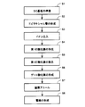
- FIG. 2 is a flowchart showing a method for manufacturing the SiC semiconductor device according to the first embodiment of the present invention.
- 3 to 10 are cross-sectional views schematically showing each manufacturing process of the SiC semiconductor device according to the first embodiment of the present invention.
- a method for manufacturing an SiC semiconductor device according to an embodiment of the present invention will be described.
- a MOSFET Metal Oxide Semiconductor Field Effect Transistor
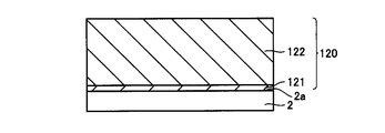
- SiC substrate 2 having a surface 2a is prepared (step S1).
- SiC substrate 2 is not particularly limited, but can be prepared, for example, by the following method.
- a SiC ingot grown by a vapor phase growth method such as a growth method, a liquid phase growth method such as a flux method, or a high nitrogen pressure solution method is prepared. Thereafter, a SiC substrate having a surface is cut out from the SiC ingot.
- the cutting method is not particularly limited, and the SiC substrate is cut from the SiC ingot by slicing or the like.
- the surface of the cut SiC substrate is polished.
- the surface to be polished may be only the front surface, or the back surface opposite to the front surface may be further polished.
- the method of polishing is not particularly limited, but CMP (Chemical Mechanical Polishing), for example, can be employed to flatten the surface and reduce damage such as scratches.
- CMP Chemical Mechanical Polishing
- colloidal silica is used as an abrasive, diamond
- chromium oxide is used as abrasive grains
- an adhesive, wax, or the like is used as a fixing agent.
- other polishing such as an electric field polishing method, a chemical polishing method, and a mechanical polishing method may be further performed. Polishing may be omitted.
- the cleaning method is not particularly limited. For example, after the oxide film is formed by thermal oxidation or the like, cleaning by removing the oxide film by thermal decomposition or thermal etching can be employed. Cleaning may be omitted.
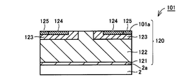
- the SiC substrate 2 having the surface 2a shown in FIG. 3 can be prepared.
- SiC substrate 2 for example, a substrate having an n-type conductivity and a resistance of 0.02 ⁇ cm is used.
- the epitaxial layer 120 is formed on the surface 2a of the SiC substrate 2 by vapor phase growth, liquid phase growth, or the like (step S2).
- epitaxial layer 120 is formed as follows, for example.
- buffer layer 121 is formed on surface 2 a of SiC substrate 2.
- Buffer layer 121 is an epitaxial layer made of, for example, n-type SiC and having a thickness of 0.5 ⁇ m, for example.
- the concentration of conductive impurities in the buffer layer 121 is, for example, 5 ⁇ 10 17 cm ⁇ 3 .
- a breakdown voltage holding layer 122 is formed on the buffer layer 121.
- a layer made of SiC of n-type conductivity is formed by a vapor phase growth method, a liquid phase growth method, or the like.
- the thickness of the breakdown voltage holding layer 122 is, for example, 15 ⁇ m.
- the concentration of the n-type conductive impurity in the breakdown voltage holding layer 122 is, for example, 5 ⁇ 10 15 cm ⁇ 3 .
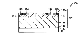
- ions are implanted into the epitaxial layer 120 (step S3).
- a p-type well region 123, an n + source region 124, and a p + contact region 125 are formed as follows.
- a well region 123 is formed by selectively injecting p-type impurities into a part of the breakdown voltage holding layer 122.
- a source region 124 is formed by selectively injecting an n-type conductive impurity into a predetermined region, and a contact is formed by selectively injecting a p-type conductive impurity into the predetermined region.
- Region 125 is formed.
- the impurity is selectively implanted using a mask made of an oxide film, for example. This mask is removed after the implantation of impurities.
- Activating annealing may be performed after such step S3 for ion implantation.
- annealing is performed in an argon atmosphere at a heating temperature of 1700 ° C. for 30 minutes.
- step S3 for ion implantation surface cleaning such as organic cleaning, acid cleaning, and RCA cleaning may be further performed.
- an epitaxial wafer 100 including the SiC substrate 2 and the epitaxial layer 120 formed on the SiC substrate 2 can be prepared.
- the surface 100a (first surface) of the epitaxial wafer 100 (SiC semiconductor) is cleaned.
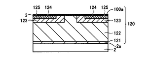
- the first oxide film 3 is formed on the surface 100a of the epitaxial wafer 100 (step S4).
- the first oxide film 3 is, for example, silicon oxide.
- the first oxide film 3 is formed by the first forming unit 11 of the manufacturing apparatus 10 shown in FIG.
- the method for forming the first oxide film 3 is not particularly limited, and a method of oxidizing the surface 100a of the epitaxial wafer 100 using, for example, thermal oxidation in an atmosphere containing a solution containing O, O plasma, O gas, or the like. Used.
- the solution containing O means a solution containing oxygen, for example, ozone water.
- ozone water having a concentration of, for example, 30 ppm or more. In this case, the decomposition of ozone can be suppressed, and the reaction rate between the surface 100a of the epitaxial wafer 100 and ozone can be increased, so that the first oxide film 3 can be easily formed on the surface 100a.
- O gas means a gas containing oxygen
- thermal oxidation containing O gas is preferably performed in a dry atmosphere at a temperature of 700 ° C. or higher, for example, considering that SiC is a stable compound.
- the dry atmosphere means that the first oxide film 3 is formed in the gas phase, and may include an unintended liquid phase component.
- O plasma means plasma generated from a gas containing oxygen, and can be generated, for example, by supplying oxygen gas (O 2 ) to a plasma generator.
- “Forming the first oxide film 3 by O plasma” means forming the first oxide film 3 by plasma using a gas containing oxygen. In other words, it means that the first oxide film 3 is formed by processing with plasma generated from a gas containing oxygen.
- step S4 when the purpose is to remove impurities and particles adhering to the surface 100a, for example, the thickness of one molecular layer or more and 10 nm or less (thickness in the direction from the surface 100a toward the SiC substrate 2).
- 1 oxide film 3 is formed.
- impurities, particles, and the like attached to the surface 100a can be taken into the surface and the inside of the first oxide film 3.
- the oxide film having a thickness of 10 nm or less the first oxide film 3 is easily removed in step S5 described later.
- liquid phase cleaning wet cleaning
- gas phase cleaning dry cleaning
- the damaged layer is removed in step S4. Oxidize.
- first oxide film 3 having a thickness of more than 10 nm and not more than 100 nm is formed.
- impurities, particles and the like attached to the surface 100a can be taken into the first oxide film 3.
- cleaning by a gas phase dry cleaning
- the damage layer has surface roughness compared to other regions, for example, by performing SIMS analysis, excessive silicon or carbon (C) is present compared to the non-implanted region. Specified by.
- the epitaxial wafer 100 on which the first oxide film 3 is formed by the first formation unit 11 is transferred to the removal unit 12.
- the epitaxial wafer 100 is transferred in the second connection portion 15 which is an atmosphere in which the atmosphere is blocked.
- the epitaxial wafer 100 is placed in an atmosphere in which air is blocked.
- step S5 of the present embodiment the first oxide film 3 is removed by the removing unit 12 of the manufacturing apparatus 10 shown in FIG.
- the method for removing the first oxide film 3 is not particularly limited, and for example, wet etching, dry etching, thermal decomposition, F plasma, or the like can be used.
- the first oxide film 3 is removed using a solution such as HF or NH 4 F (ammonium fluoride).
- the dry etching is at least one selected from the group consisting of hydrogen gas, hydrogen chloride gas, sulfur fluoride gas, and fluorocarbon gas at 800 ° C. or higher and lower than or equal to SiC sublimation temperature, preferably 1000 ° C. or higher and lower than SiC sublimation temperature. It is preferable to remove the first oxide film 3 using a gas containing one of the two. Hydrogen gas, hydrogen chloride gas, sulfur fluoride gas, and fluorocarbon gas at 800 ° C. or higher have a high effect of reducing the first oxide film 3. From this viewpoint, 1000 ° C. or higher is more preferable.
- the first oxide film is SiO x
- hydrogen gas decomposes SiO x into H 2 O and SiH y
- hydrogen chloride gas decomposes SiO x into H 2 O and SiCl z .
- Deterioration of the epitaxial wafer 100 can be suppressed by setting the temperature to a sublimation temperature of SiC or lower. Also, dry etching is preferably performed under reduced pressure from the viewpoint of promoting the reaction.
- the thermal decomposition is preferably performed by thermally decomposing the first oxide film 3 at 1200 ° C. or higher and SiC sublimation temperature or lower in an oxygen-free atmosphere.
- the first oxide film 3 formed on the surface 100a of the epitaxial wafer 100 is heated in an atmosphere not containing oxygen at 1200 ° C. or higher, the first oxide film 3 can be easily pyrolyzed.
- Degradation of the epitaxial wafer 100 can be suppressed by setting the temperature to a sublimation temperature of SiC or lower.
- F plasma means plasma generated from a gas containing fluorine (F), for example, carbon tetrafluoride gas (CF 4 ), trifluoromethane gas (CHF 3 ), Freon gas (C 2 F 6 ), six Sulfur fluoride gas (SF 6 ), nitrogen trifluoride gas (NF 3 ), xenon difluoride gas (XeF 2 ), fluorine gas (F 2 ), and chlorine trifluoride gas (ClF 3 ) alone or It can generate
- “Removing the first oxide film 3 by F plasma” means removing the first oxide film 3 by plasma using a gas containing fluorine. In other words, it means that the first oxide film 3 is removed by processing with plasma generated from a gas containing fluorine.
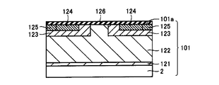
- step S5 By performing step S5, the first oxide film 3 that has taken in impurities, particles, and the like in step S4 is removed, so that impurities, particles, and the like on the surface 100a of the epitaxial wafer 100 can be removed. Thereby, as shown in FIG. 7, an epitaxial wafer 101 having a surface 101a (second surface) in which impurities, particles, and the like are reduced can be formed.
- the damaged layer can be further removed by performing step S5.
- an epitaxial wafer 101 having a surface 101a in which impurities, particles, and the like are reduced can be formed.
- an epitaxial wafer 101 having a surface 101a from which impurities, particles, and the like are reduced and from which a damaged layer is removed can be formed.
- steps S4 and S5 may be repeated. Moreover, you may implement by adding the washing
- the other chemical liquid include SPM containing sulfuric acid and hydrogen peroxide solution.
- SPM sulfuric acid
- organic substances can be removed.
- step S5 for removing the first oxide film 3 and step S6 for forming a gate oxide film 126 described later even when shifting to another process.
- the epitaxial wafer is placed in an atmosphere where the atmosphere is blocked.
- the epitaxial wafer 101 from which the first oxide film 3 has been removed by the removing unit 12 is transferred to the second forming unit 13.
- the epitaxial wafer 101 is transported in the first connection portion 14 which is an atmosphere in which air is blocked.
- the epitaxial wafer 101 is placed in an atmosphere in which the atmosphere is blocked. .
- the second surface constituting the SiC semiconductor device is formed on the surface 101 a (second surface) exposed by removing the first oxide film 3 in the epitaxial wafer 101.
- a gate oxide film 126 as an oxide film is formed (step S6). Specifically, as shown in FIG. 8, a gate oxide film 126 is formed so as to cover the breakdown voltage holding layer 122, the well region 123, the source region 124, and the contact region 125. This formation can be performed, for example, by thermal oxidation (dry oxidation). Thermal oxidation is performed by heating to a high temperature in an atmosphere containing oxygen such as O 2 , O 3 , and N 2 O.
- the thermal oxidation conditions are, for example, a heating temperature of 1200 ° C. and a heating time of 30 minutes.
- the formation of the gate oxide film 126 is not limited to thermal oxidation, and may be formed by, for example, a CVD method or a sputtering method.
- Gate oxide film 126 is made of a silicon oxide film having a thickness of 50 nm, for example.
- step S5 for removing the first oxide film 3 and step S6 for forming the gate oxide film 126.
- step S5 for removing the first oxide film 3
- step S6 for forming the gate oxide film 126.
- the difference in temperature between the epitaxial wafers 100 and 101 between step S4 for forming the first oxide film 3, step S5 for removing the first oxide film 3, and step S6 for forming the gate oxide film 126. is more preferably maintained at 500 ° C. or lower. In this case, since the temperature difference of the epitaxial wafer is small between the start of step S4 and the end of step S6, the throughput can be improved.
- the epitaxial wafer 101 having the cleaned surface 101a it is preferable to hold the epitaxial wafer 101 having the cleaned surface 101a at 800 ° C. or higher between step S5 for removing the first oxide film 3 and step S6 for forming the gate oxide film 126. It is more preferable to hold at 1000 ° C. or higher. In this case, since the temperature drop of the epitaxial wafer between step S5 and step S6 can be suppressed, the throughput can be improved.
- the epitaxial wafers 100 and 101 are formed between the step S4 for forming the first oxide film 3, the step S5 for removing the first oxide film 3, and the step S6 for forming the gate oxide film 126, respectively. It is preferable to hold at 800 ° C. or higher, and more preferable to hold at 1000 ° C. or higher. In this case, since the temperature drop of the epitaxial wafer can be suppressed from the start of step S4 to the end of step S6, the throughput can be improved.
- nitrogen annealing is performed (step S7). Specifically, an annealing process is performed in a nitrogen monoxide (NO) atmosphere.
- the heating temperature is 1100 ° C. and the heating time is 120 minutes.
- nitrogen atoms can be introduced in the vicinity of the interface between each of the breakdown voltage holding layer 122, the well region 123, the source region 124, and the contact region 125 and the gate oxide film 126.
- an annealing process using an argon gas which is an inert gas may be performed after the annealing process using the nitric oxide.
- the conditions for this treatment are, for example, a heating temperature of 1100 ° C. and a heating time of 60 minutes.
- step S7 surface cleaning such as organic cleaning, acid cleaning, and RCA cleaning may be further performed.
- step S8 electrodes are formed (step S8).
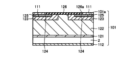
- the source electrode 111 shown in FIG. 9 is formed as follows. Specifically, a resist film having a pattern is formed on the gate oxide film 126 by using a photolithography method. Using this resist film as a mask, portions of gate oxide film 126 located on source region 124 and contact region 125 are removed by etching. As a result, an opening 126 a is formed in the gate oxide film 126.
- a conductor film is formed by vapor deposition so as to be in contact with each of the source region 124 and the contact region 125 in the opening 126a.
- the conductor film may be a metal film, and is made of nickel (Ni), for example. As a result of this lift-off, the source electrode 111 is formed.
- the heat processing for alloying is performed here.
- heat treatment is performed for 2 minutes at a heating temperature of 950 ° C. in an atmosphere of argon (Ar) gas that is an inert gas.
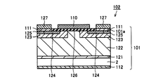
- an upper source electrode 127 is formed on the source electrode 111 by, for example, vapor deposition.
- drain electrode 112 is formed on the back surface of SiC substrate 2 by, for example, vapor deposition.
- the gate electrode 110 is formed as follows, for example. A resist film having an opening pattern located in a region on the gate oxide film 126 is formed in advance, and a conductor film constituting a gate electrode is formed so as to cover the entire surface of the resist film. Then, by removing the resist film, the conductor film other than the portion of the conductor film to be the gate electrode is removed (lifted off). As a result, the gate electrode 110 can be formed on the gate oxide film 126 as shown in FIG.
- MOSFET 102 as the SiC semiconductor device shown in FIG. 10 can be manufactured.
- the SiC substrate 2 is used to manufacture the MOSFET 102, the material of the substrate is not limited to SiC, and may be manufactured using crystals of other materials. Further, the SiC substrate 2 may be omitted.
- the method for manufacturing MOSFET 102 as an example of the SiC semiconductor device according to the present embodiment includes the step S5 for removing first oxide film 3 and the gate oxidation that constitutes MOSFET 102 as the second oxide film. Between step S6 of forming the film 126, the epitaxial wafer 101 as the SiC semiconductor is placed in an atmosphere in which the atmosphere is blocked.
- MOSFET 102 manufacturing apparatus 10 as an example of the SiC semiconductor device according to the present embodiment includes a first connection portion 14 that connects removal portion 12 and second formation portion 13 so that epitaxial wafer 101 can be transported.
- the region where the epitaxial wafer 101 is transported in one connecting portion 14 can be shut off from the atmosphere.
- step S4 for forming the first oxide film impurities such as titanium (Ti), particles, etc. adhering to the surface 100a of the epitaxial wafer 100 are first removed.
- the oxide film 3 can be incorporated.
- step S5 of removing the first oxide film 3 impurities, particles, and the like attached to the surface 100a of the epitaxial wafer 100 can be removed.
- step S6 for forming the gate oxide film 126 the gate oxide film 126 constituting the SiC semiconductor device can be formed on the surface 101a of the epitaxial wafer 101 in this state. Impurities and particles present at the interface can be reduced. In addition, since the surface 101a of the epitaxial wafer 101 can be kept clean, impurities, particles, and the like present in the gate oxide film 126 formed on the surface 101a can be reduced. Furthermore, the film quality of the gate oxide film 126 can be improved. Therefore, the withstand voltage when the reverse voltage is applied to the MOSFET 102 can be improved, and the stability and long-term reliability of the operation when the forward voltage is applied can be improved. Therefore, the MOSFET 102 that can improve the characteristics can be manufactured.
- the first oxide film 3 is formed on the surface of the epitaxial wafer 100, and after the surface is cleaned by removing the first oxide film 3, the epitaxial wafer 101 is exposed to the atmosphere. Reducing the possibility of recontamination. Since SiC is a stable compound, it is not easy to form the first oxide film 3 on the surface 100a of the epitaxial wafer 100 as compared with Si. For this reason, after cleaning the surface 100a of the epitaxial wafer 100, which is a SiC semiconductor, transferring the epitaxial wafer 101 to the next step (step S6 for forming a gate oxide film) without exposing it to the atmosphere simplifies the cleaning. And greatly contributes to the improvement of the characteristics of the manufactured SiC semiconductor device.
- the removal portion 12 for removing the first oxide film 3 and the second formation portion 13 are mutually connected. It becomes difficult to bring in contaminants such as particles and impurities. Similarly, it is possible to reduce the possibility of bringing in contamination between steps S5 for removing the first oxide film 3 and step S6 for forming the gate oxide film 126. For this reason, since the removal part 12 and the 2nd formation part 13 can be maintained clean, it contributes greatly to the improvement of the characteristic of the SiC semiconductor device to manufacture.
- step S4 for forming first oxide film 3, step S5 for removing first oxide film 3, and gate oxide film 126 are preferable.
- the epitaxial wafers 100 and 101 are placed in an atmosphere in which the atmosphere is shut off between the step S6 and the step S6.
- second connection portion 15 that connects first formation portion 11 and removal portion 12 is further provided so that epitaxial wafer 100 can be transported.
- the region where the epitaxial wafer 101 is transported in the second connection portion 15 can be shielded from the atmosphere.
- the epitaxial wafer 101 can be prevented from being exposed to the atmosphere from the start to the end of the cleaning process, and the epitaxial wafer 101 can be suppressed from being exposed to the atmosphere from the end of the cleaning process to the formation of the gate oxide film. For this reason, since it can suppress that the surface 100a, 101a of the epitaxial wafers 100 and 101 during washing
- a MOSFET manufacturing method has been described as an example of a SiC semiconductor device.
- the present invention describes a SiC epitaxial wafer having a surface and an oxidation forming a SiC semiconductor device formed on the surface.
- the present invention can be applied to a semiconductor device provided with a film (an oxide film remaining as a SiC semiconductor device).
- SiC epitaxial wafers include those that are ion-implanted from the surface and those that are not ion-implanted.
- the present invention is a semiconductor device having an insulated gate field effect section such as a MOSFET or IGBT (Insulated Gate Bipolar Transistor), or a JFET (Junction Field-Effect Transistor).
- the present invention can be applied to all SiC semiconductor devices having an oxide film.
- FIG. 11 is a schematic diagram of a SiC semiconductor device manufacturing apparatus according to the second embodiment of the present invention.
- the SiC semiconductor device manufacturing apparatus according to the second embodiment will be described with reference to FIG.
- the manufacturing apparatus 20 of the present embodiment includes a chamber 21, a first gas supply unit 22, a second gas supply unit 23, and a vacuum pump 24.
- the first gas supply unit 22, the second gas supply unit 23, and the vacuum pump 24 are connected to the chamber 21.
- the chamber 21 accommodates the epitaxial wafers 100 and 101 (see FIGS. 5 to 7).
- a plasma generator can be used as the chamber 21, for example.
- the first gas supply unit 22 forms an oxide film (this embodiment) for forming the first oxide film 3 (see FIG. 6) on the epitaxial wafer 100 and constituting the SiC semiconductor device (MOSFET 102 in this embodiment).
- a gas used to form a gate oxide film 126) (see FIG. 8) is supplied to the chamber 21.
- the first gas supply unit 22 supplies a gas containing oxygen, for example.
- the second gas supply unit 23 supplies a gas used to remove the first oxide film 3 formed on the epitaxial wafer 100 to the chamber 21.
- the second gas supply unit 23 supplies a gas for reducing silicon (Si) and oxygen such as H 2 gas and HCl gas to the chamber 21.
- the vacuum pump 24 evacuates the inside of the chamber 21. Therefore, after forming the first oxide film 3 on the epitaxial wafer 100 by the first gas supply unit 22, the inside of the chamber 21 is evacuated and the first oxide film 3 is formed by the second gas supply unit 23. Can be removed. Further, after removing the first oxide film 3, the inside of the chamber 21 is evacuated, and the second gas film (gate oxide film 126) constituting the SiC semiconductor device is formed by the first gas supply unit 22 as an epitaxial wafer. 101 can be formed.
- the vacuum pump 24 may be omitted.
- manufacturing apparatus 20 shown in FIG. 11 may include various elements other than the above, illustration and description of these elements are omitted for convenience of explanation.
- the manufacturing method of the SiC semiconductor device according to the present embodiment is the same as that of the first embodiment, except that the MOSFET 102 shown in FIG. 9 is manufactured. However, the manufacturing method 20 shown in FIG. 11 is different. Therefore, between step S4 for forming the first oxide film and step S5 for removing the first oxide film, and step S5 for removing the first oxide film and step S6 for forming the gate oxide film 126. Since the epitaxial wafer is placed in the chamber 21, the atmosphere is shielded from the atmosphere.
- the gate oxide film 126 as the second oxide film can be formed using the apparatus used in step S5 for removing the first oxide film 3.
- step S5 for removing the first oxide film 3 and step S6 for forming the gate oxide film 126 are performed by the same apparatus. Therefore, the temperature of the epitaxial wafer can be kept as low as possible (for example, 500 ° C. or less) between step S5 for removing the first oxide film and step S6 for forming the gate oxide film. Further, the temperature of the epitaxial wafer can be maintained at 800 ° C. or higher, preferably 1000 ° C. or higher, between step S 5 for removing the first oxide film and step S 6 for forming the gate oxide film.
- step S4 for forming the first oxide film 3, step S5 for removing the first oxide film 3, and step S6 for forming the gate oxide film 126 are performed by the same apparatus. Is done. Therefore, the step S4 for forming the first oxide film 3 and the step S5 for removing the first oxide film 3 and the step S5 for removing the first oxide film 3 and the gate oxide film 126 are formed.
- the temperature of the epitaxial wafer can be kept as low as possible (for example, 500 ° C. or lower). Further, between step S4 for forming the first oxide film and step S5 for removing the first oxide film, and between step S5 for removing the first oxide film and step S6 for forming the gate oxide film. In the meantime, the temperature of the epitaxial wafer can be maintained at 800 ° C. or higher, preferably 1000 ° C. or higher.
- step S4 for forming the first oxide film 3 and after step S5 for removing the first oxide film 3 the inside of the chamber 21 is evacuated by the vacuum pump 24 (for example, up to 0.1 Pa or less). It is preferable to evacuate.
- the pressure of the atmosphere is preferably reduced (for example, reduced to 0.1 Pa or less).
- the step S5 for removing the first oxide film 3 is switched between the step S5 for removing the first oxide film 3 and the step S6 for forming the gate oxide film 126.
- the Si decomposed in step 1 generation of SiO 2 particles formed by the reaction between the remaining Si and the O 2 gas introduced to form the gate oxide film 126 can be reduced.
- the surface of the epitaxial wafer can be made cleaner. That is, the generation of particles associated with gas switching can be suppressed.
- the first oxide film 3 is removed, and the surface exposed by removing the first oxide film 3 from the epitaxial wafer 100 is A chamber 21 for forming a gate oxide film 126) as a second oxide film constituting the MOSFET 102 as the SiC semiconductor device is provided.
- a chamber 21 for forming a gate oxide film 126) as a second oxide film constituting the MOSFET 102 as the SiC semiconductor device is provided.
- step S6 for forming the gate oxide film 126 the gate oxide film 126 constituting the MOSFET 102 as the SiC semiconductor device can be formed on the surface 101a of the epitaxial wafer 101 in this state. Impurities, particles, etc. existing at the interface with 126 can be reduced. In addition, since the surface 101a of the epitaxial wafer 101 can be kept clean, impurities, particles, and the like present in the gate oxide film 126 can be reduced. Further, the film quality of the gate oxide film 126 formed on the surface 101a can be improved. Therefore, the withstand voltage when the reverse voltage is applied to the MOSFET 102 can be improved, and the stability and long-term reliability of the operation when the forward voltage is applied can be improved. Therefore, the MOSFET 102 that can improve the characteristics can be manufactured.
- the first formation portion for forming the first oxide film 3 on the surface 100 a of the epitaxial wafer 100 and the first oxide film 3 are removed, and the first oxide film 3 is removed from the epitaxial wafer 100.
- the manufacturing apparatus 20 which is the same as the second forming portion for forming the gate oxide film 126 constituting the MOSFET 102 on the surface 101a exposed by removing the oxide film 3 has been described as an example.
- the first forming unit and the second forming unit may be different devices. That is, in the manufacturing apparatus of the present invention, the second forming unit has the configuration shown in FIG. 11, and the first forming unit may be arranged separately from the second forming unit.
- the manufacturing apparatus further includes a connecting portion that connects the first forming portion and the second forming portion so that the SiC semiconductor can be transported, and the region where the SiC semiconductor is transported in the connecting portion is shielded from the atmosphere.
- a connecting portion that connects the first forming portion and the second forming portion so that the SiC semiconductor can be transported, and the region where the SiC semiconductor is transported in the connecting portion is shielded from the atmosphere.
Landscapes
- Electrodes Of Semiconductors (AREA)
- Chemical & Material Sciences (AREA)
- Crystallography & Structural Chemistry (AREA)
- Formation Of Insulating Films (AREA)
- Insulated Gate Type Field-Effect Transistor (AREA)
- Cleaning Or Drying Semiconductors (AREA)
Abstract
Description
図1は、本発明の実施の形態1におけるSiC半導体装置の製造装置を示す模式図である。図1を参照して、本発明の一実施の形態におけるSiC半導体装置の製造装置10を説明する。
図11は、本発明の実施の形態2におけるSiC半導体装置の製造装置の模式図である。図11などを参照して、本実施の形態2におけるSiC半導体装置の製造装置を説明する。
Claims (12)
- 炭化珪素半導体装置(102)を製造する方法であって、
炭化珪素半導体の第1の表面(100a)に第1の酸化膜(3)を形成する工程と、
前記第1の酸化膜(3)を除去する工程と、
前記炭化珪素半導体において前記第1の酸化膜(3)が除去されることにより露出した第2の表面(101a)に、前記炭化珪素半導体装置(102)を構成する第2の酸化膜(126)を形成する工程とを備え、
前記第1の酸化膜(3)を除去する工程と、前記第2の酸化膜(126)を形成する工程との間において、前記炭化珪素半導体は大気が遮断された雰囲気内に配置される、炭化珪素半導体装置(102)の製造方法。 - 前記第1の酸化膜(3)を形成する工程と、前記第1の酸化膜(3)を除去する工程との間において、前記炭化珪素半導体は大気が遮断された雰囲気内に配置される、請求項1に記載の炭化珪素半導体装置(102)の製造方法。
- 前記第1の酸化膜(3)を形成する工程では、前記炭化珪素半導体の前記第1の表面(100a)に形成されたダメージ層を酸化する、請求項1に記載の炭化珪素半導体装置(102)の製造方法。
- 前記第1の酸化膜(3)を除去する工程は、酸素を含まない雰囲気で1200℃以上炭化珪素の昇華温度以下で前記第1の酸化膜(3)を熱分解する工程と、800℃以上炭化珪素の昇華温度以下で水素ガス、塩化水素ガス、フッ化硫黄ガスおよびフッ化炭素ガスからなる群から選択される少なくとも1つを含むガスを用いてエッチングする工程との少なくとも一方を含む、請求項1に記載の炭化珪素半導体装置(102)の製造方法。
- 前記第1の酸化膜(3)を除去する工程と前記第2の酸化膜(126)を形成する工程との間において、前記炭化珪素半導体の温度差を500℃以下に保持する、請求項1に記載の炭化珪素半導体装置の製造方法。
- 前記第2の酸化膜(126)を形成する工程では、前記第1の酸化膜(3)を除去する工程で用いる装置を用いて、前記第2の酸化膜(126)を形成する、請求項5に記載の炭化珪素半導体装置(102)の製造方法。
- 前記第1の酸化膜(3)を形成する工程と、前記第1の酸化膜(3)を除去する工程と、前記第2の酸化膜(126)を形成する工程とのそれぞれの間において、前記炭化珪素半導体の温度差を500℃以下に保持する、請求項2に記載の炭化珪素半導体装置(1002)の製造方法。
- 前記第1の酸化膜(3)を形成する工程で用いる装置と、前記第1の酸化膜(3)を除去する工程で用いる装置と、前記第2の酸化膜を形成する工程で用いる装置とが同一である、請求項7に記載の炭化珪素半導体装置の製造方法。
- 炭化珪素半導体装置(102)を製造する装置(10)であって、
炭化珪素半導体の第1の表面(100a)に第1の酸化膜(3)を形成するための第1の形成部(11)と、
前記第1の酸化膜(3)を除去するための除去部(12)と、
前記除去部(12)で、前記炭化珪素半導体において前記第1の酸化膜(3)が除去されることにより露出した第2の表面(101a)に、前記炭化珪素半導体装置(102)を構成する第2の酸化膜(126)を形成するための第2の形成部(13)と、
前記炭化珪素半導体を搬送可能に前記除去部(12)と前記第2の形成部(13)とを接続する第1の接続部(14)とを備え、
前記第1の接続部(14)における前記炭化珪素半導体を搬送させる領域は、大気の遮断が可能である、炭化珪素半導体装置(102)の製造装置。 - 前記炭化珪素半導体を搬送可能に前記第1の形成部(11)と前記除去部(12)とを接続する第2の接続部(15)をさらに備え、
前記第2の接続部(15)における前記炭化珪素半導体を搬送させる領域は、大気の遮断が可能である、請求項9に記載の炭化珪素半導体装置(102)の製造装置(10)。 - 炭化珪素半導体装置(102)を製造する装置であって、
炭化珪素半導体の第1の表面(100a)に第1の酸化膜(3)を形成するための第1の形成部と、
前記第1の酸化膜(3)を除去し、かつ前記炭化珪素半導体において前記第1の酸化膜(3)が除去されることにより露出した第2の表面(101a)に、前記炭化珪素半導体装置を構成する第2の酸化膜(126)を形成するための第2の形成部とを備えた、炭化珪素半導体装置の製造装置(20)。 - 前記第1の形成部と前記第2の形成部とは、同一である、請求項11に記載の炭化珪素半導体装置の製造装置(20)。
Priority Applications (5)
| Application Number | Priority Date | Filing Date | Title |
|---|---|---|---|
| KR1020127010182A KR20130076790A (ko) | 2010-06-16 | 2011-02-25 | 탄화규소 반도체 장치의 제조 방법 및 탄화규소 반도체 장치의 제조 장치 |
| CN201180004388.7A CN102986009B (zh) | 2010-06-16 | 2011-02-25 | 用于制造碳化硅半导体装置的方法和设备 |
| US13/502,976 US9184276B2 (en) | 2010-06-16 | 2011-02-25 | Method and apparatus for manufacturing silicon carbide semiconductor device |
| CA2778197A CA2778197A1 (en) | 2010-06-16 | 2011-02-25 | Method and apparatus for manufacturing silicon carbide semiconductor device |
| EP11795441.2A EP2584592A4 (en) | 2010-06-16 | 2011-02-25 | METHOD FOR PRODUCING A SILICON CARBIDE SEMICONDUCTOR COMPONENT AND DEVICE FOR PRODUCING A SILICON CARBIDE SEMICONDUCTOR COMPONENT |
Applications Claiming Priority (2)
| Application Number | Priority Date | Filing Date | Title |
|---|---|---|---|
| JP2010136870A JP5605005B2 (ja) | 2010-06-16 | 2010-06-16 | 炭化珪素半導体装置の製造方法および炭化珪素半導体装置の製造装置 |
| JP2010-136870 | 2010-06-16 |
Publications (1)
| Publication Number | Publication Date |
|---|---|
| WO2011158533A1 true WO2011158533A1 (ja) | 2011-12-22 |
Family
ID=45347945
Family Applications (1)
| Application Number | Title | Priority Date | Filing Date |
|---|---|---|---|
| PCT/JP2011/054332 Ceased WO2011158533A1 (ja) | 2010-06-16 | 2011-02-25 | 炭化珪素半導体装置の製造方法および炭化珪素半導体装置の製造装置 |
Country Status (8)
| Country | Link |
|---|---|
| US (1) | US9184276B2 (ja) |
| EP (1) | EP2584592A4 (ja) |
| JP (1) | JP5605005B2 (ja) |
| KR (1) | KR20130076790A (ja) |
| CN (1) | CN102986009B (ja) |
| CA (1) | CA2778197A1 (ja) |
| TW (1) | TW201203386A (ja) |
| WO (1) | WO2011158533A1 (ja) |
Cited By (2)
| Publication number | Priority date | Publication date | Assignee | Title |
|---|---|---|---|---|
| WO2013145022A1 (ja) * | 2012-03-30 | 2013-10-03 | 株式会社日立製作所 | 炭化珪素半導体装置の製造方法 |
| JPWO2013145022A1 (ja) * | 2012-03-30 | 2015-08-03 | 株式会社日立製作所 | 炭化珪素半導体装置の製造方法 |
Families Citing this family (8)
| Publication number | Priority date | Publication date | Assignee | Title |
|---|---|---|---|---|
| JP2015061001A (ja) * | 2013-09-20 | 2015-03-30 | 株式会社東芝 | 半導体装置の製造方法 |
| JP6248532B2 (ja) * | 2013-10-17 | 2017-12-20 | セイコーエプソン株式会社 | 3C−SiCエピタキシャル層の製造方法、3C−SiCエピタキシャル基板および半導体装置 |
| JP6844176B2 (ja) * | 2016-09-29 | 2021-03-17 | 富士電機株式会社 | 炭化珪素半導体装置および炭化珪素半導体装置の製造方法 |
| US20180233574A1 (en) * | 2017-02-10 | 2018-08-16 | Purdue Research Foundation | Silicon carbide power transistor apparatus and method of producing same |
| CN109003895B (zh) * | 2018-07-19 | 2021-06-08 | 大连理工大学 | 一种提高SiC MOSFET器件性能稳定性的制作方法 |
| JP7294097B2 (ja) * | 2019-12-04 | 2023-06-20 | 株式会社デンソー | 半導体装置の製造方法 |
| WO2022130788A1 (ja) * | 2020-12-18 | 2022-06-23 | 国立大学法人京都大学 | SiC半導体素子の製造方法及びSiCMOSFET |
| US20220336203A1 (en) * | 2021-04-15 | 2022-10-20 | Globalwafers Co., Ltd. | Fabrication method of semiconductor substrate |
Citations (4)
| Publication number | Priority date | Publication date | Assignee | Title |
|---|---|---|---|---|
| JPH06314679A (ja) | 1993-04-30 | 1994-11-08 | Sony Corp | 半導体基板の洗浄方法 |
| JP2002075908A (ja) * | 2000-09-01 | 2002-03-15 | National Institute Of Advanced Industrial & Technology | 炭化珪素半導体装置およびその製造方法 |
| JP2002093800A (ja) * | 2000-09-14 | 2002-03-29 | Nissan Motor Co Ltd | 炭化珪素半導体装置の製造方法 |
| JP2009064955A (ja) * | 2007-09-06 | 2009-03-26 | Mitsubishi Electric Corp | 炭化珪素半導体装置の製造方法 |
Family Cites Families (18)
| Publication number | Priority date | Publication date | Assignee | Title |
|---|---|---|---|---|
| US5272107A (en) | 1983-09-24 | 1993-12-21 | Sharp Kabushiki Kaisha | Manufacture of silicon carbide (SiC) metal oxide semiconductor (MOS) device |
| JPS6066866A (ja) * | 1983-09-24 | 1985-04-17 | Sharp Corp | 炭化珪素mos構造の製造方法 |
| JPH0952796A (ja) * | 1995-08-18 | 1997-02-25 | Fuji Electric Co Ltd | SiC結晶成長方法およびSiC半導体装置 |
| JP3105770B2 (ja) * | 1995-09-29 | 2000-11-06 | 日本電気株式会社 | 半導体装置の製造方法 |
| EP0845803A4 (en) * | 1996-04-18 | 2002-03-27 | Matsushita Electric Industrial Co Ltd | SiC ELEMENT AND PROCESS FOR ITS PRODUCTION |
| JP3085272B2 (ja) * | 1997-12-19 | 2000-09-04 | 富士電機株式会社 | 炭化けい素半導体装置の熱酸化膜形成方法 |
| JP3959856B2 (ja) * | 1998-07-31 | 2007-08-15 | 株式会社デンソー | 炭化珪素半導体装置及びその製造方法 |
| JP2000349081A (ja) | 1999-06-07 | 2000-12-15 | Sony Corp | 酸化膜形成方法 |
| TW484170B (en) * | 1999-11-30 | 2002-04-21 | Applied Materials Inc | Integrated modular processing platform |
| JP3534056B2 (ja) * | 2000-08-31 | 2004-06-07 | 日産自動車株式会社 | 炭化珪素半導体装置の製造方法 |
| JP4678672B2 (ja) * | 2005-03-09 | 2011-04-27 | 誠 後藤 | 発音学習装置及び発音学習プログラム |
| JP2006321707A (ja) | 2005-04-22 | 2006-11-30 | Bridgestone Corp | 炭化ケイ素単結晶ウェハ及びその製造方法 |
| JP2007053227A (ja) * | 2005-08-18 | 2007-03-01 | Matsushita Electric Ind Co Ltd | 半導体素子およびその製造方法 |
| US7572741B2 (en) * | 2005-09-16 | 2009-08-11 | Cree, Inc. | Methods of fabricating oxide layers on silicon carbide layers utilizing atomic oxygen |
| JP2008098200A (ja) * | 2006-10-05 | 2008-04-24 | Kiyoyoshi Mizuno | 成膜体およびその製造方法 |
| JP4600438B2 (ja) * | 2007-06-21 | 2010-12-15 | 株式会社デンソー | 炭化珪素半導体装置の製造方法 |
| JP2009212366A (ja) * | 2008-03-05 | 2009-09-17 | Oki Semiconductor Co Ltd | 半導体装置の製造方法 |
| JP2010147730A (ja) * | 2008-12-18 | 2010-07-01 | Nec Corp | ネットワーク装置、ipネットワークシステム及び呼制御方法 |
-
2010
- 2010-06-16 JP JP2010136870A patent/JP5605005B2/ja not_active Expired - Fee Related
-
2011
- 2011-02-25 CA CA2778197A patent/CA2778197A1/en not_active Abandoned
- 2011-02-25 KR KR1020127010182A patent/KR20130076790A/ko not_active Withdrawn
- 2011-02-25 WO PCT/JP2011/054332 patent/WO2011158533A1/ja not_active Ceased
- 2011-02-25 CN CN201180004388.7A patent/CN102986009B/zh not_active Expired - Fee Related
- 2011-02-25 US US13/502,976 patent/US9184276B2/en not_active Expired - Fee Related
- 2011-02-25 EP EP11795441.2A patent/EP2584592A4/en not_active Ceased
- 2011-04-11 TW TW100112515A patent/TW201203386A/zh unknown
Patent Citations (4)
| Publication number | Priority date | Publication date | Assignee | Title |
|---|---|---|---|---|
| JPH06314679A (ja) | 1993-04-30 | 1994-11-08 | Sony Corp | 半導体基板の洗浄方法 |
| JP2002075908A (ja) * | 2000-09-01 | 2002-03-15 | National Institute Of Advanced Industrial & Technology | 炭化珪素半導体装置およびその製造方法 |
| JP2002093800A (ja) * | 2000-09-14 | 2002-03-29 | Nissan Motor Co Ltd | 炭化珪素半導体装置の製造方法 |
| JP2009064955A (ja) * | 2007-09-06 | 2009-03-26 | Mitsubishi Electric Corp | 炭化珪素半導体装置の製造方法 |
Non-Patent Citations (1)
| Title |
|---|
| See also references of EP2584592A4 |
Cited By (2)
| Publication number | Priority date | Publication date | Assignee | Title |
|---|---|---|---|---|
| WO2013145022A1 (ja) * | 2012-03-30 | 2013-10-03 | 株式会社日立製作所 | 炭化珪素半導体装置の製造方法 |
| JPWO2013145022A1 (ja) * | 2012-03-30 | 2015-08-03 | 株式会社日立製作所 | 炭化珪素半導体装置の製造方法 |
Also Published As
| Publication number | Publication date |
|---|---|
| JP5605005B2 (ja) | 2014-10-15 |
| JP2012004273A (ja) | 2012-01-05 |
| CN102986009A (zh) | 2013-03-20 |
| TW201203386A (en) | 2012-01-16 |
| EP2584592A1 (en) | 2013-04-24 |
| KR20130076790A (ko) | 2013-07-08 |
| US9184276B2 (en) | 2015-11-10 |
| CA2778197A1 (en) | 2011-12-22 |
| CN102986009B (zh) | 2016-02-03 |
| US20120208368A1 (en) | 2012-08-16 |
| EP2584592A4 (en) | 2014-12-10 |
Similar Documents
| Publication | Publication Date | Title |
|---|---|---|
| JP5605005B2 (ja) | 炭化珪素半導体装置の製造方法および炭化珪素半導体装置の製造装置 | |
| WO2012070368A1 (ja) | 炭化珪素半導体装置の製造方法および炭化珪素半導体装置の製造装置 | |
| US20120178259A1 (en) | Method of cleaning silicon carbide semiconductor and apparatus for cleaning silicon carbide semiconductor | |
| US10199221B2 (en) | Cleaning method | |
| WO2011158528A1 (ja) | 炭化珪素半導体装置の製造方法および炭化珪素半導体装置の製造装置 | |
| JP2012004275A (ja) | 炭化珪素半導体装置の製造方法 | |
| TWI821158B (zh) | 用於半導體製程的整合系統 | |
| CN102549723A (zh) | 碳化硅半导体的清洗方法 | |
| US20120174944A1 (en) | Cleaning method for silicon carbide semiconductor and cleaning apparatus for silicon carbide semiconductor |
Legal Events
| Date | Code | Title | Description |
|---|---|---|---|
| WWE | Wipo information: entry into national phase |
Ref document number: 201180004388.7 Country of ref document: CN |
|
| 121 | Ep: the epo has been informed by wipo that ep was designated in this application |
Ref document number: 11795441 Country of ref document: EP Kind code of ref document: A1 |
|
| WWE | Wipo information: entry into national phase |
Ref document number: 2778197 Country of ref document: CA |
|
| WWE | Wipo information: entry into national phase |
Ref document number: 13502976 Country of ref document: US |
|
| ENP | Entry into the national phase |
Ref document number: 20127010182 Country of ref document: KR Kind code of ref document: A |
|
| WWE | Wipo information: entry into national phase |
Ref document number: 2011795441 Country of ref document: EP |
|
| NENP | Non-entry into the national phase |
Ref country code: DE |