WO2011158811A1 - 光半導体装置用リードフレーム、光半導体装置用リードフレームの製造方法、および光半導体装置 - Google Patents
光半導体装置用リードフレーム、光半導体装置用リードフレームの製造方法、および光半導体装置 Download PDFInfo
- Publication number
- WO2011158811A1 WO2011158811A1 PCT/JP2011/063542 JP2011063542W WO2011158811A1 WO 2011158811 A1 WO2011158811 A1 WO 2011158811A1 JP 2011063542 W JP2011063542 W JP 2011063542W WO 2011158811 A1 WO2011158811 A1 WO 2011158811A1
- Authority
- WO
- WIPO (PCT)
- Prior art keywords
- optical semiconductor
- semiconductor device
- lead frame
- alloy
- silver
- Prior art date
- Legal status (The legal status is an assumption and is not a legal conclusion. Google has not performed a legal analysis and makes no representation as to the accuracy of the status listed.)
- Ceased
Links
Images





Classifications
-
- H—ELECTRICITY
- H10—SEMICONDUCTOR DEVICES; ELECTRIC SOLID-STATE DEVICES NOT OTHERWISE PROVIDED FOR
- H10H—INORGANIC LIGHT-EMITTING SEMICONDUCTOR DEVICES HAVING POTENTIAL BARRIERS
- H10H20/00—Individual inorganic light-emitting semiconductor devices having potential barriers, e.g. light-emitting diodes [LED]
- H10H20/80—Constructional details
- H10H20/85—Packages
- H10H20/857—Interconnections, e.g. lead-frames, bond wires or solder balls
-
- C—CHEMISTRY; METALLURGY
- C25—ELECTROLYTIC OR ELECTROPHORETIC PROCESSES; APPARATUS THEREFOR
- C25D—PROCESSES FOR THE ELECTROLYTIC OR ELECTROPHORETIC PRODUCTION OF COATINGS; ELECTROFORMING; APPARATUS THEREFOR
- C25D5/00—Electroplating characterised by the process; Pretreatment or after-treatment of workpieces
- C25D5/10—Electroplating with more than one layer of the same or of different metals
-
- C—CHEMISTRY; METALLURGY
- C25—ELECTROLYTIC OR ELECTROPHORETIC PROCESSES; APPARATUS THEREFOR
- C25D—PROCESSES FOR THE ELECTROLYTIC OR ELECTROPHORETIC PRODUCTION OF COATINGS; ELECTROFORMING; APPARATUS THEREFOR
- C25D5/00—Electroplating characterised by the process; Pretreatment or after-treatment of workpieces
- C25D5/10—Electroplating with more than one layer of the same or of different metals
- C25D5/12—Electroplating with more than one layer of the same or of different metals at least one layer being of nickel or chromium
-
- C—CHEMISTRY; METALLURGY
- C25—ELECTROLYTIC OR ELECTROPHORETIC PROCESSES; APPARATUS THEREFOR
- C25D—PROCESSES FOR THE ELECTROLYTIC OR ELECTROPHORETIC PRODUCTION OF COATINGS; ELECTROFORMING; APPARATUS THEREFOR
- C25D5/00—Electroplating characterised by the process; Pretreatment or after-treatment of workpieces
- C25D5/34—Pretreatment of metallic surfaces to be electroplated
-
- C—CHEMISTRY; METALLURGY
- C25—ELECTROLYTIC OR ELECTROPHORETIC PROCESSES; APPARATUS THEREFOR
- C25D—PROCESSES FOR THE ELECTROLYTIC OR ELECTROPHORETIC PRODUCTION OF COATINGS; ELECTROFORMING; APPARATUS THEREFOR
- C25D5/00—Electroplating characterised by the process; Pretreatment or after-treatment of workpieces
- C25D5/48—After-treatment of electroplated surfaces
-
- C—CHEMISTRY; METALLURGY
- C25—ELECTROLYTIC OR ELECTROPHORETIC PROCESSES; APPARATUS THEREFOR
- C25D—PROCESSES FOR THE ELECTROLYTIC OR ELECTROPHORETIC PRODUCTION OF COATINGS; ELECTROFORMING; APPARATUS THEREFOR
- C25D5/00—Electroplating characterised by the process; Pretreatment or after-treatment of workpieces
- C25D5/48—After-treatment of electroplated surfaces
- C25D5/50—After-treatment of electroplated surfaces by heat-treatment
-
- C—CHEMISTRY; METALLURGY
- C25—ELECTROLYTIC OR ELECTROPHORETIC PROCESSES; APPARATUS THEREFOR
- C25D—PROCESSES FOR THE ELECTROLYTIC OR ELECTROPHORETIC PRODUCTION OF COATINGS; ELECTROFORMING; APPARATUS THEREFOR
- C25D5/00—Electroplating characterised by the process; Pretreatment or after-treatment of workpieces
- C25D5/60—Electroplating characterised by the structure or texture of the layers
- C25D5/605—Surface topography of the layers, e.g. rough, dendritic or nodular layers
- C25D5/611—Smooth layers
-
- C—CHEMISTRY; METALLURGY
- C25—ELECTROLYTIC OR ELECTROPHORETIC PROCESSES; APPARATUS THEREFOR
- C25D—PROCESSES FOR THE ELECTROLYTIC OR ELECTROPHORETIC PRODUCTION OF COATINGS; ELECTROFORMING; APPARATUS THEREFOR
- C25D5/00—Electroplating characterised by the process; Pretreatment or after-treatment of workpieces
- C25D5/60—Electroplating characterised by the structure or texture of the layers
- C25D5/615—Microstructure of the layers, e.g. mixed structure
- C25D5/617—Crystalline layers
-
- C—CHEMISTRY; METALLURGY
- C25—ELECTROLYTIC OR ELECTROPHORETIC PROCESSES; APPARATUS THEREFOR
- C25D—PROCESSES FOR THE ELECTROLYTIC OR ELECTROPHORETIC PRODUCTION OF COATINGS; ELECTROFORMING; APPARATUS THEREFOR
- C25D5/00—Electroplating characterised by the process; Pretreatment or after-treatment of workpieces
- C25D5/627—Electroplating characterised by the visual appearance of the layers, e.g. colour, brightness or mat appearance
-
- C—CHEMISTRY; METALLURGY
- C25—ELECTROLYTIC OR ELECTROPHORETIC PROCESSES; APPARATUS THEREFOR
- C25D—PROCESSES FOR THE ELECTROLYTIC OR ELECTROPHORETIC PRODUCTION OF COATINGS; ELECTROFORMING; APPARATUS THEREFOR
- C25D7/00—Electroplating characterised by the article coated
- C25D7/08—Mirrors; Reflectors
-
- H—ELECTRICITY
- H10—SEMICONDUCTOR DEVICES; ELECTRIC SOLID-STATE DEVICES NOT OTHERWISE PROVIDED FOR
- H10H—INORGANIC LIGHT-EMITTING SEMICONDUCTOR DEVICES HAVING POTENTIAL BARRIERS
- H10H20/00—Individual inorganic light-emitting semiconductor devices having potential barriers, e.g. light-emitting diodes [LED]
- H10H20/80—Constructional details
- H10H20/85—Packages
- H10H20/855—Optical field-shaping means, e.g. lenses
- H10H20/856—Reflecting means
-
- H—ELECTRICITY
- H10—SEMICONDUCTOR DEVICES; ELECTRIC SOLID-STATE DEVICES NOT OTHERWISE PROVIDED FOR
- H10W—GENERIC PACKAGES, INTERCONNECTIONS, CONNECTORS OR OTHER CONSTRUCTIONAL DETAILS OF DEVICES COVERED BY CLASS H10
- H10W70/00—Package substrates; Interposers; Redistribution layers [RDL]
- H10W70/40—Leadframes
- H10W70/451—Multilayered leadframes
-
- H—ELECTRICITY
- H10—SEMICONDUCTOR DEVICES; ELECTRIC SOLID-STATE DEVICES NOT OTHERWISE PROVIDED FOR
- H10W—GENERIC PACKAGES, INTERCONNECTIONS, CONNECTORS OR OTHER CONSTRUCTIONAL DETAILS OF DEVICES COVERED BY CLASS H10
- H10W70/00—Package substrates; Interposers; Redistribution layers [RDL]
- H10W70/40—Leadframes
- H10W70/456—Materials
-
- C—CHEMISTRY; METALLURGY
- C25—ELECTROLYTIC OR ELECTROPHORETIC PROCESSES; APPARATUS THEREFOR
- C25D—PROCESSES FOR THE ELECTROLYTIC OR ELECTROPHORETIC PRODUCTION OF COATINGS; ELECTROFORMING; APPARATUS THEREFOR
- C25D3/00—Electroplating: Baths therefor
- C25D3/02—Electroplating: Baths therefor from solutions
- C25D3/12—Electroplating: Baths therefor from solutions of nickel or cobalt
-
- C—CHEMISTRY; METALLURGY
- C25—ELECTROLYTIC OR ELECTROPHORETIC PROCESSES; APPARATUS THEREFOR
- C25D—PROCESSES FOR THE ELECTROLYTIC OR ELECTROPHORETIC PRODUCTION OF COATINGS; ELECTROFORMING; APPARATUS THEREFOR
- C25D3/00—Electroplating: Baths therefor
- C25D3/02—Electroplating: Baths therefor from solutions
- C25D3/38—Electroplating: Baths therefor from solutions of copper
-
- C—CHEMISTRY; METALLURGY
- C25—ELECTROLYTIC OR ELECTROPHORETIC PROCESSES; APPARATUS THEREFOR
- C25D—PROCESSES FOR THE ELECTROLYTIC OR ELECTROPHORETIC PRODUCTION OF COATINGS; ELECTROFORMING; APPARATUS THEREFOR
- C25D3/00—Electroplating: Baths therefor
- C25D3/02—Electroplating: Baths therefor from solutions
- C25D3/46—Electroplating: Baths therefor from solutions of silver
-
- C—CHEMISTRY; METALLURGY
- C25—ELECTROLYTIC OR ELECTROPHORETIC PROCESSES; APPARATUS THEREFOR
- C25D—PROCESSES FOR THE ELECTROLYTIC OR ELECTROPHORETIC PRODUCTION OF COATINGS; ELECTROFORMING; APPARATUS THEREFOR
- C25D3/00—Electroplating: Baths therefor
- C25D3/02—Electroplating: Baths therefor from solutions
- C25D3/56—Electroplating: Baths therefor from solutions of alloys
- C25D3/64—Electroplating: Baths therefor from solutions of alloys containing more than 50% by weight of silver
-
- C—CHEMISTRY; METALLURGY
- C25—ELECTROLYTIC OR ELECTROPHORETIC PROCESSES; APPARATUS THEREFOR
- C25D—PROCESSES FOR THE ELECTROLYTIC OR ELECTROPHORETIC PRODUCTION OF COATINGS; ELECTROFORMING; APPARATUS THEREFOR
- C25D5/00—Electroplating characterised by the process; Pretreatment or after-treatment of workpieces
- C25D5/02—Electroplating of selected surface areas
- C25D5/022—Electroplating of selected surface areas using masking means
-
- C—CHEMISTRY; METALLURGY
- C25—ELECTROLYTIC OR ELECTROPHORETIC PROCESSES; APPARATUS THEREFOR
- C25D—PROCESSES FOR THE ELECTROLYTIC OR ELECTROPHORETIC PRODUCTION OF COATINGS; ELECTROFORMING; APPARATUS THEREFOR
- C25D5/00—Electroplating characterised by the process; Pretreatment or after-treatment of workpieces
- C25D5/34—Pretreatment of metallic surfaces to be electroplated
- C25D5/36—Pretreatment of metallic surfaces to be electroplated of iron or steel
-
- C—CHEMISTRY; METALLURGY
- C25—ELECTROLYTIC OR ELECTROPHORETIC PROCESSES; APPARATUS THEREFOR
- C25D—PROCESSES FOR THE ELECTROLYTIC OR ELECTROPHORETIC PRODUCTION OF COATINGS; ELECTROFORMING; APPARATUS THEREFOR
- C25D5/00—Electroplating characterised by the process; Pretreatment or after-treatment of workpieces
- C25D5/34—Pretreatment of metallic surfaces to be electroplated
- C25D5/42—Pretreatment of metallic surfaces to be electroplated of light metals
- C25D5/44—Aluminium
-
- H—ELECTRICITY
- H10—SEMICONDUCTOR DEVICES; ELECTRIC SOLID-STATE DEVICES NOT OTHERWISE PROVIDED FOR
- H10H—INORGANIC LIGHT-EMITTING SEMICONDUCTOR DEVICES HAVING POTENTIAL BARRIERS
- H10H20/00—Individual inorganic light-emitting semiconductor devices having potential barriers, e.g. light-emitting diodes [LED]
- H10H20/80—Constructional details
- H10H20/85—Packages
- H10H20/8506—Containers
Definitions
- the present invention relates to an optical semiconductor device lead frame, a manufacturing method thereof, and an optical semiconductor device.
- the reflective material of the lead frame has a high reflectance in the entire visible light wavelength range (400 to 800 nm) (for example, the reflectance with respect to a reference material such as barium sulfate or aluminum oxide). 80% or more).
- the use of LEDs that emit ultraviolet rays has been expanded, such as light sources for measuring / analyzing instruments that use ultraviolet rays, photocatalytic air purifiers, ultraviolet sensors, and light sources for curing ultraviolet curable resins.
- optical semiconductor devices using LED elements have come to be used.
- a layer (film) made of silver or a silver alloy is formed on the lead frame on which the LED element is mounted, particularly for the purpose of improving the light reflectance in the visible light region (hereinafter referred to as reflectance). ) Is often formed.
- the silver film has a high reflectance in the visible light region.
- a silver plating layer is formed on the reflection surface (Patent Document 1), or 200 or after the silver or silver alloy film is formed. It is known that a heat treatment is performed at a temperature of not lower than 30 ° C. for 30 seconds or longer, and the crystal grain size of the film is 0.5 ⁇ m to 30 ⁇ m (Patent Document 2).
- the absorption peak in the near ultraviolet region also affects the reflectance in the visible light region (near 400 nm to 800 nm). It has also led to a decline. This problem is particularly apparent at wavelengths near the near ultraviolet region.
- the luminous efficiency of the LED is improved year by year, it is still about 20%, so that the reflectance is low by 10% means a significant reduction in luminance. For this reason, when using a chip having a wavelength of 340 to 400 nm, which is in the near ultraviolet region, it is necessary to improve the reflectance in this wavelength region. By improving the reflectance of the lead frame material, it is possible to improve the luminance around one LED.
- Patent Document 3 has no knowledge about optical characteristics such as reflectance, and is not a rolling process for the purpose of improving reflectance.
- low-temperature annealing heat treatment
- the substrate component diffused to the surface layer due to the heating and lowered the reflectivity.
- the contact surface is maintained because the new surface is exposed by sliding and good conduction is obtained.
- the state of the outermost surface contributes most to the optical reflection phenomenon, so that the reflectivity is considered to decrease. From this, it can be seen that simply by rolling after plating and annealing, it cannot be easily developed for an optical semiconductor lead frame.
- the luminous efficiency of the LED module is affected by the reflectance of the lead frame surface as well as the luminous efficiency of the LED chip. If the reflectivity of the lead frame surface is low, not only the light emission efficiency of the LED module is lowered, but also the heat generation on the lead frame surface is increased and the sealing resin is deteriorated. . For this reason, when an LED module having high color rendering properties using an LED chip that emits ultraviolet light is to be realized, there is a strong demand for improving the reflectivity of the lead frame in the near ultraviolet region with a wavelength of 340 to 400 nm.
- the emission wavelength of the optical semiconductor chip mounted on the white LED module is still mainly around 450 nm.
- the improvement in the reflectance in the visible light region is very effective in improving the luminance of the LED module, and it is required to be as close as possible to the theoretical reflectance of the silver film (the reflectance is about 98% at 450 nm).
- the reflectance is about 98% at 450 nm.
- even in the case of a film made of a metal other than silver or an alloy thereof it has been required to achieve a high reflectance in the near ultraviolet region to the visible light region, which is required as an optical semiconductor lead frame.
- the present invention provides a lead frame for an optical semiconductor device used in LEDs, photocouplers, photointerrupters, and the like that include a near-ultraviolet to visible light range (wavelength 340 to 800 nm) in the emission wavelength. 400nm), particularly in the vicinity of a wavelength of 375nm and in the visible light region (wavelength of 400 to 800nm), particularly in the case of mounting a chip that emits light in the vicinity of a wavelength of 450nm.
- the task is to do.
- Another object is to provide an optical semiconductor device and an illumination device using the lead frame.
- the present inventors have formed an optical semiconductor device in which a reflective layer made of a metal or an alloy thereof, such as silver or a silver alloy, is formed by plating on the outermost surface of the substrate.
- the reflection layer is not necessary in the vicinity of a wavelength of 345 nm to 355 nm by applying a mechanical process such as rolling after forming the plated layer to crush the plated structure into a mechanically deformed metal structure.
- a lead frame for a semiconductor device can be obtained that can eliminate or remarkably suppress a large absorption peak and is excellent in the reflectance of light in the near ultraviolet region having a wavelength of 340 to 400 nm.
- the reflectance in the visible light region can be improved by several percent compared to the conventional silver plating film, and can be made close to the theoretical value of silver to the limit, and is made of a metal other than silver or an alloy thereof.
- coatings by achieving high reflectivity from the near ultraviolet region to the visible light region required for optical semiconductor lead frames, it is possible to obtain lead frames for semiconductor devices that have excellent light reflectivities. I found it.
- the crystal grain boundary of the silver plating film that has been conventionally used is the cause of the decrease in reflectance.
- the structure obtained by plating grows in the length, width, and thickness direction after nucleation in the substrate, but the bonding strength between adjacent silver crystals is weak, and metallurgically produced silver. It was found that the interval between the grains was wider than the grain boundary. And it turned out that the fall of a reflectance can be suppressed by narrowing the space
- the inventors of the present invention have developed a lead frame for an optical semiconductor device in which the outermost reflective layer on the conductive substrate is formed by a plating method. It has been found that the rate can be improved and the resin adhesion can be increased. By setting the surface roughness to a small range and a predetermined range in a micro surface shape, unnecessary absorption peaks in the near ultraviolet region, particularly around 345 nm to 355 nm can be eliminated or significantly suppressed, and at the same time visible It has been found that the reflectance is improved over the entire light region.
- the adhesion between the lead frame material and the sealing material (hereinafter referred to as resin adhesion) is improved by setting the surface roughness within a certain range in the macro surface shape. It has been found that the surface smoothness is improved by controlling the two surface roughnesses, macro surface roughness and micro surface roughness, to improve the reflectance while improving the resin adhesion.
- resin adhesion the adhesion between the lead frame material and the sealing material
- An optical semiconductor device lead frame comprising a reflective layer on at least one side or both sides of the outermost surface of the substrate, partly or entirely, wherein the reflective layer emits at least light emitted by the optical semiconductor element.
- a lead frame for an optical semiconductor device characterized in that at the outermost surface of the reflective region, at least the surface of a plating structure made of metal or an alloy thereof has a mechanically deformed structure.
- the reflective layer has a surface roughness Ra measured by a contact needle surface roughness meter of 0.010 ⁇ m or more and a surface roughness Sa measured by an atomic force microscope of 50 nm or less.
- the metal forming the reflective layer or its alloy is silver, silver-tin alloy, silver-indium alloy, silver-rhodium alloy, silver-ruthenium alloy, silver-gold alloy, silver-palladium alloy, silver-nickel
- the lead frame for an optical semiconductor device according to (1) or (5) which is an alloy, a silver-selenium alloy, a silver-antimony alloy, or a silver-platinum alloy.
- the base includes n metal layers (n is an integer of 1 or more) thereon, and the reflective layer is provided on the base directly or via at least one of the metal layers.
- the lead frame for an optical semiconductor device according to any one of (1) to (7), wherein (9) A plating layer made of any one of silver, a silver alloy, tin, a tin alloy, gold, or a gold alloy is provided at least in a portion that requires soldering, (1) to (8) The lead frame for optical semiconductor devices according to any one of the above. (10) A method for manufacturing a material for a lead frame for a semiconductor device according to any one of (1) to (8), wherein at least light emitted from an optical semiconductor element is reflected on an outermost surface of a substrate.
- An optical semiconductor device characterized in that a reflective layer made of a metal or an alloy thereof is formed in a region by a plating method, and then mechanically processed to mechanically deform at least a plated structure on the surface of the reflective layer.
- Lead frame material manufacturing method (11)
- the mechanical processing after forming the reflective layer is performed by rolling and the processing rate at the time of the rolling processing is set to 1% to 80%, or the processing rate at the time of the press processing performed by pressing is 1%.
- mechanical processing is performed to obtain a lead frame material for an optical semiconductor device in which at least the plating structure of the surface of the reflective layer is mechanically deformed.
- a method for producing a lead frame for an optical semiconductor device wherein a lead frame is obtained by subjecting a material to a punching process by a pressing method or an etching method.
- the mechanical processing after forming the reflective layer is performed by rolling, and the processing rate at the time of the rolling processing is set to 1% to 80%, or the processing rate at the time of the press processing performed by pressing is 1%.
- the plating with good solderability is applied to at least a region other than a region that reflects light emitted from the optical semiconductor element, and the plating component is silver, silver alloy, tin, tin alloy, gold, or The method for manufacturing a lead frame for an optical semiconductor device according to item (14), wherein the method is any one of gold alloys.
- An optical semiconductor device comprising an optical semiconductor element and the lead frame for an optical semiconductor device according to any one of (1) to (9), wherein the optical semiconductor device lead frame includes: The reflective layer is provided on the outermost surface of the substrate and reflects at least light generated from the optical semiconductor element, and at least the plated structure on the surface has a mechanically deformed structure.
- optical semiconductor device (17) The optical semiconductor device according to (16), wherein an emission wavelength of the optical semiconductor element is 340 nm to 800 nm. (18) The optical semiconductor device according to (16) or (17), wherein the light output from the device is white light. (19) The optical semiconductor device according to (16) or (17), wherein the light output from the device is ultraviolet, near ultraviolet, or violet light. (20) An illumination device comprising the optical semiconductor device according to any one of (16) to (19).
- a plating layer such as an electroplating method, an electroless plating method, or a sputtering method is applied to a reflective layer made of a metal or an alloy thereof, such as silver or a silver alloy, on the outermost surface on the substrate.
- the reflective layer is further subjected to mechanical processing such as rolling to mechanically deform at least the surface of the plated structure, thereby eliminating the above-described unnecessary absorption peak in the vicinity of the wavelength of 345 nm to 355 nm.
- the reflectance at 340 to 400 nm, which is in the near ultraviolet region, is improved, and a good reflectance is obtained particularly in an optical semiconductor device mounted with an optical semiconductor chip whose emission wavelength includes a wavelength in the near ultraviolet region. It is done. Furthermore, the reflectance can be improved to the theoretical value level of the silver film by the same method, and the reflectivity at the wavelength range of 400 to 800 nm can be improved.
- an optical semiconductor By achieving high reflectivity from the near ultraviolet region to the visible light region, which is required as a lead frame, both are good, for example, in a conventional optical semiconductor device mounted on an optical semiconductor chip with an emission wavelength of around 450 nm. Reflectivity can be obtained.
- a light-emitting chip having good reflection characteristics over a wide range from the near-ultraviolet light to the visible light region, in particular, a wavelength of 340 to 400 nm, and further combined with this is a visible light region of 400 to 800 nm.
- a lead frame for an optical semiconductor device which is superior in reflection characteristics than a conventional silver plating material. Further, by using this optical semiconductor device lead frame, a high-intensity optical semiconductor device and illumination device can be provided.
- the reflective layer is further subjected to mechanical processing such as rolling.
- the visible The reflectance at a wavelength of 400 to 800 nm, which is the light region can be increased to 85% or more, and further, at a wavelength of 450 nm or more, the reflectance can be increased to 90% or more.
- it has an excellent effect in improving the reflectance in the near ultraviolet region.
- heat dissipation is superior to that formed directly on a circuit on a mounting substrate, and deterioration of the optical semiconductor device due to heat can be delayed.
- the lead frame for an optical semiconductor device of the present invention for example, LED component material
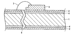
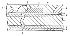
- FIG. 1 is a schematic cross-sectional view of a first embodiment of a lead frame for an optical semiconductor device according to the present invention.
- FIG. 2 is a schematic sectional view of a second embodiment of the lead frame for an optical semiconductor device according to the present invention.
- FIG. 3 is a schematic sectional view of a third embodiment of the lead frame for an optical semiconductor device according to the present invention.
- FIG. 4 is a schematic cross-sectional view of a fourth embodiment of the lead frame for optical semiconductor devices according to the present invention.
- FIG. 5 is a schematic sectional view of a fifth embodiment of a lead frame for an optical semiconductor device according to the present invention.
- FIG. 6 is a schematic sectional view of a sixth embodiment of a lead frame for an optical semiconductor device according to the present invention.
- FIG. 7 is a schematic sectional view of a seventh embodiment of the lead frame for an optical semiconductor device according to the present invention.
- FIG. 8 is a graph showing the reflectance of the lead frame for an optical semiconductor device of Invention Example 19 according to the present invention together with the reflectance of Conventional Example 1.
- a metal such as silver or a silver alloy or a layer of an alloy thereof as a reflective layer is initially formed by a plating method, and further, mechanical processing (for example, plastic processing such as rolling) is performed on the layer. Then, the metal structure (plating structure) formed by the plating method has a reflective layer in which at least the surface thereof is mechanically deformed by mechanical processing.
- the plating method may be a wet plating method such as an electroplating method or an electroless plating method, or a dry plating method such as a sputtering method.
- the mechanical processing may be plastic processing such as rolling or pressing, or mechanical polishing using colloidal silica or the like.
- plastic processing such as rolling or pressing, or mechanical polishing using colloidal silica or the like.
- the entire material including the base body undergoes plastic working, so that the entire plated structure undergoes plastic deformation.
- mechanical polishing the surface of the plated structure is smoothed and subjected to mechanical deformation including the surface of the substrate.
- the metallographic structure (plating structure) formed by electroplating, electroless plating, or sputtering is applied to the plating structure by plastic working such as rolling or pressing, or mechanical polishing. It has a reflective layer whose surface is mechanically deformed at least on the outermost surface.
- the plastically deformed metal structure is different from the cast structure as is metallurgically clear in the present technical field, and is also different from the plated structure before deformation formed by plating. Specifically, fine crystals are usually observed on the surface after plating, and a needle-like structure, a precipitated state of spherical particles, and the like are observed.
- the surface state after rolling or pressing after plating exhibits surface properties such that the processing pattern formed on the rolls of the rolling rolls or the surface of the press mold is transferred to the lead frame side. Therefore, the surface can be clearly distinguished by performing surface observation with a general-purpose SEM at an observation magnification of 2000 to 10,000 times, for example.
- a general-purpose SEM at an observation magnification of 2000 to 10,000 times, for example.
- mechanical polishing is performed after plating, it can be confirmed that the processing alteration layer seen by the polishing streaks and cross-sectional observation of the abrasive paper and abrasive grains is formed on the outermost layer. It can be clearly distinguished from later states.
- the lead frame of the present invention not only the wavelength range of 340 to 400 nm but also the visible light wavelength range of 400 to 800 nm can reach the physical theoretical value of the reflectance of silver as much as possible. This is because the reflectivity is about 98% at a wavelength of 450 nm when pure silver is formed on a mirror substrate such as silicon by sputtering. However, it is easy to use a brightener by simply plating. It is a numerical value that cannot be achieved. In the case of a film made of a metal other than silver or an alloy thereof, a high reflectance in the near ultraviolet region to the visible light region required as an optical semiconductor lead frame can be achieved.
- the present inventors cause mechanical deformation in the plated structure by performing mechanical processing such as rolling after plating, reduce fine irregularities by crushing the plated structure, and reduce crystal grain boundaries. As a result of extinction, the light absorption phenomenon was reduced to the limit. As a result, it was clarified that the reflectance can be brought close to the theoretical value even in the visible light region. As a result, by using the lead frame according to the present invention, excellent luminance can be obtained even in a conventional optical semiconductor device in the visible light region, and a blue light emitting element having a wavelength region of 400 to 800 nm, particularly an emission wavelength of around 450 nm is mounted. It is suitably used for an optical semiconductor device.
- the reflective layer made of a metal or an alloy thereof according to the present invention is formed on the outermost surface of at least a portion that contributes to light reflection (that is, at least a region that reflects light emitted from the optical semiconductor element). It only has to be. In other portions, it is not necessary to provide a reflective layer, and even if a layer other than the reflective layer is formed, there is no particular problem in terms of reflectance.
- a plating method for example, electroplating method, electroless plating method or sputtering method
- a conductive substrate for example, strip material
- a reflective layer made of a metal or an alloy thereof, such as silver or a silver alloy
- mechanical processing such as rolling, pressing, or mechanical polishing (for example, polishing using colloidal silica) is performed.
- the shape of the lead frame is formed by pressing or etching.
- a chip mounting portion is formed on the lead frame by a resin mold or the like, and an optical semiconductor module is manufactured by mounting an optical semiconductor chip, wire bonding, and sealing with resin or glass containing a phosphor.
- a conductive base such as a strip
- silver plating or gold / palladium / nickel plating is performed.
- it attaches to predetermined heat processing after metal plating, and makes the particle size of a plating layer coarse.
- the present invention and the conventional method are the ones in which the present invention is a modification of the plating structure as a mechanical processing finish, whereas the conventional method is a simple processing finish by cladding, plating finish or heat treatment finish, or The structure is completely different in that the heat treatment for plating and rolling is improved.
- the processing rate (or area reduction rate) at the time of plastic processing such as rolling or pressing after forming the reflective layer is 1% or more in the portion used as the reflective layer.
- the higher the processing rate the better the reflection characteristics and the higher the brightness of the LED lead frame. If the processing rate during plastic processing such as rolling after forming the reflective layer exceeds 80%, not only the effect of improving the reflection characteristics is saturated, but also cracks and cracks during bending are likely to occur. % Or less is preferable.
- the “machining rate” indicates a ratio represented by “(plate thickness before processing ⁇ plate thickness after processing) ⁇ 100 / (plate thickness before processing)”.
- location used as a reflective layer means that when an optical semiconductor module is formed, an optical semiconductor module is obtained by resin-molding a portion other than the light emitting portion, but the optical semiconductor chip emits light. In this case, it means a portion where the lead frame is exposed and a portion where light reflection occurs.
- the lead frame for an optical semiconductor device of the present invention has good reflectance characteristics and can easily form a film by using copper or a copper alloy, iron or an iron alloy, or aluminum or an aluminum alloy as a base.
- a lead frame that can contribute to cost reduction can be provided.
- the lead frame based on these metals or alloys has excellent heat dissipation characteristics, and the heat energy generated when the light emitter emits light can be smoothly discharged to the outside through the lead frame, and light emission It is expected that the lifetime of the element will be prolonged and the reflectance characteristics will be stabilized over a long period of time. This depends on the conductivity of the substrate, preferably at least 10% in IACS (International Annealed Copper Standard), more preferably 50% or more.
- IACS International Annealed Copper Standard
- the lead frame for an optical semiconductor device of the present invention has a reflective layer thickness of 0.2 ⁇ m or more after mechanical processing such as rolling made of metal or an alloy thereof, for example, silver or a silver alloy,
- the reflectivity can be stably increased, and deterioration due to heating in a subsequent process such as wire bonding, sealing with resin or glass can be suppressed.
- the upper limit of the thickness of the reflective layer after mechanical processing such as rolling is preferably 10 ⁇ m or less from the viewpoint of reduction of silver as a noble metal and plating processing cost. When it is thinner than the lower limit (for example, 0.1 ⁇ m), discoloration due to heating occurs and the rate of improvement in reflectance is small. For this reason, in order to prevent discoloration due to heating more stably, the thickness of the reflective layer after mechanical processing such as rolling is preferably 0.5 ⁇ m or more.
- the silver or silver alloy forming the reflective layer in the lead frame for optical semiconductor devices of the present invention is silver, silver-tin alloy, silver-indium alloy, silver-rhodium alloy, silver-ruthenium alloy, silver-gold alloy, By using a material selected from the group consisting of a silver-palladium alloy, a silver-nickel alloy, a silver-selenium alloy, a silver-antimony alloy, and a silver-platinum alloy, a lead frame with good reflectivity and good productivity can be obtained.
- silver, silver-tin alloy, silver-indium alloy, silver-palladium alloy, silver-selenium alloy, or silver-antimony alloy are more preferable from the viewpoint of improving the reflectance.
- nickel, nickel alloy, cobalt, cobalt alloy, copper, and the like are provided between the base and the reflective layer made of metal or an alloy thereof (for example, silver or silver alloy).
- An intermediate layer made of a metal or alloy selected from the group consisting of copper alloys may be provided.
- the intermediate layer is suitably formed by plating, for example.
- the thermal conductivity of the material is relatively low. Therefore, by providing a copper or copper alloy layer as an intermediate layer, the heat dissipation can be improved without impairing the reflectance. Furthermore, since the plating layer which is the copper or copper alloy layer contributes to the improvement of plating adhesion, it is possible to prevent deterioration of adhesion due to heat generation when the light emitting element emits light.
- a nickel, nickel alloy, cobalt, or cobalt alloy layer is used as an intermediate layer in order to suppress diffusion of the substrate component to the reflective layer due to heat generated when the light emitting element emits light. It is effective to provide it.
- the improvement of the resin is also progressing, and in some cases, glass sealing is being performed, and during the sealing process with resin or glass
- the processing temperature is also rising.
- an optical semiconductor device such as an LED
- the diffusion phenomenon is expected to proceed due to heat generated by the LED chip.
- it is effective to provide an intermediate layer.
- the thickness of these intermediate layers is not particularly limited in the present invention, but is preferably in the range of 0.08 to 2.0 ⁇ m.
- the thickness of the intermediate layer is particularly preferably in the range of 0.2 to 2.0 ⁇ m.
- the processing rate at the time of mechanical processing such as rolling after forming the reflective layer is set to 1% or more as the processing rate based on the plate thickness immediately after the initial formation of the reflective layer (immediately after plating).
- a lead frame having a reflectance improved by several percent over silver or a silver alloy film obtained by the plating method can be obtained even at a wavelength of 400 to 800 nm, which is a visible light region, while preventing a decrease in reflectance due to the appearance of an absorption peak.
- the processing rate at the time of mechanical processing, such as rolling processing after formation of a reflective layer is less than 1%, mechanical deformation such as plastic deformation is insufficient, and its effect is small.
- the number of rolling is preferably 3 times or less at most.
- the processing rate at the time of rolling after the reflective layer is formed may be 1% or more in each rolling.
- the processing rate during the rolling process after the formation of the reflective layer is 10% or more in total.
- the processing rate at the time of rolling after forming the reflective layer is too large, the plating thickness increases at the time of initial formation of the reflective layer (during plating), resulting in not only an increase in plating cost but also an environmental load.
- the processing cost increases due to the increase in the number of rolling processes after the reflective layer is formed and the effect of improving the reflectance is saturated, the reflective layer is formed because the cracks and cracks are likely to occur during bending.
- the processing rate in the subsequent rolling process is 80% or less in total.
- the total processing rate is more preferably 20 to 60% in consideration of bending workability.
- heat treatment also referred to as tempering or low-temperature annealing
- a technique such as batch type or running type after mechanical processing such as rolling.
- the bonding force between the crystal grains can be strengthened at the crystal grain boundaries to narrow the intergranular spacing, but it is necessary to limit the heat treatment to a level that does not lower the reflectivity.
- the conditions for the heat treatment performed after mechanical processing such as rolling are not particularly limited.
- the heat treatment is performed at a temperature of 50 to 150 ° C. for 0.08 to 3 hours. It is preferable. If the temperature of this heat treatment is too high or the time is too long, the heat history becomes excessive and the reflectance is lowered.
- the reflective layer on the surface made of a metal such as silver or a silver alloy or an alloy thereof may be formed by wet plating using an electroplating method or an electroless plating method, or alternatively, the metal may be formed by sputtering.
- the substrate surface may be formed by plating and precipitating.
- the electroplating method has been described as a representative example.
- a metal such as silver or a silver alloy is used in the same manner as in the case of the electroplating method.
- a layer made of the alloy can be formed.
- the electroless plating method it may be formed by using a commercially available bath (for example, S.Dia. Ag40; manufactured by Sasaki Chemical Co., Ltd.), etc. Can be used.
- the thickness of the reflective layer made of a metal such as silver or silver alloy or an alloy thereof after mechanical processing such as rolling is not particularly limited, but may be in the range of 0.5 to 10 ⁇ m. preferable.
- the coating thickness (initial thickness) before processing for achieving the thickness after mechanical processing is not particularly limited, but is preferably in the range of 1 to 50 ⁇ m, for example.
- Mechanical processing to a material in which a part or all of the conductive substrate is coated with a metal such as silver or a silver alloy or an alloy thereof can be performed, for example, by rolling with a cold rolling mill.
- the rolling machine includes a 2-stage roll, a 4-stage roll, a 6-stage roll, a 12-stage roll, a 20-stage roll, and the like, and any rolling machine can be used.
- the processing rate (area reduction rate) in rolling or pressing is 1% or more, preferably 10% or more, and the gap between the grain boundaries of silver or silver alloy is sufficiently narrowed to form a plastic deformation structure. Can do.
- the rolling roll used for the rolling process is preferably less than 0.1 ⁇ m in terms of the arithmetic average (Ra) of the surface roughness in consideration of improving the reflectance on the lead frame side formed by transferring the rolls.
- Ra arithmetic average
- plastic processing by cold rolling processing has been described, but in the case of press processing (for example, coining) or mechanical polishing (for example, polishing by colloidal silica), it is always the case.
- press processing for example, coining
- mechanical polishing for example, polishing by colloidal silica
- plastic processing and mechanical surface processing can be performed in the same manner as in the case of cold rolling.
- it can be achieved by adjusting the working rate by pressure adjustment at a press pressure of 0.1 N / mm 2 or more and plastically deforming.
- colloidal silica having a particle size of 10 to 300 nm is dispersed to control the number of polishing seconds and adjust the degree of processing.
- the degree of processing varies depending on the abrasive grains used and the polishing time. For example, in the case of polishing with colloidal silica (OP-S suspension: manufactured by Marumoto Struers), 10 to 60 seconds. It is preferable to set the polishing time as follows.
- the optical semiconductor device of the present invention is provided at least at a place where light generated from the optical semiconductor element is reflected by plating made of a metal such as silver or a silver alloy or an alloy thereof, and is mechanical such as a rolling process.
- a metal such as silver or a silver alloy or an alloy thereof
- the lead frame of the present invention having a reflective layer with a layer whose whole is plastically deformed or at least its surface is mechanically deformed by processing, it is possible to effectively obtain reflectance characteristics at low cost. be able to. This is because the reflectance characteristics are sufficiently effective by forming a reflective layer made of silver or a silver alloy only on the mounting portion of the optical semiconductor element.
- the optical semiconductor element mounting surface of the double-sided plating material may be thickened and the non-mounting surface may be thinned.
- a reflective layer made of a metal such as silver or a silver alloy or an alloy thereof may be partially formed, and formed by partial plating such as single-sided plating, stripe plating, spot plating, etc. It may be formed by mechanical processing. Manufacturing a lead frame in which the reflective layer is partially formed can reduce the amount of metal used in the part where the reflective layer is unnecessary, so that a lead frame with a low environmental load can be obtained. Fewer optical semiconductor devices can be obtained.
- the substrate is exposed to the end face of the lead frame inevitably obtained because it is processed into a predetermined lead frame shape by performing stamping or etching. If the lead frame after pressing or etching is stored with the substrate exposed, there is a concern about corrosion of the substrate component or deterioration of solderability to the surface of the substrate.
- the exposed area of the substrate is very small with respect to the entire surface, and there is almost no effect on the solderability with external leads. Further, the exposure of the substrate does not cause a problem even in the case of a thin plate thickness or a wide lead width. However, in the case of a thick plate thickness or a narrow lead width, soldering with a lead may affect the soldering, and the reliability of soldering is enhanced when the external lead is plated.
- solder wetting is improved by applying a plating film (soldering improvement layer) with good solder wetting, such as silver, tin, gold, and alloys of these, at least on the external lead parts that are soldered outside the reflective area .
- soldering improvement layer good solder wetting, such as silver, tin, gold, and alloys of these, at least on the external lead parts that are soldered outside the reflective area .
- the plating type may be a metal type that achieves the purpose, such as silver, tin, gold, or alloy plating thereof.
- the reflective layer is further subjected to plastic processing such as rolling or pressing, or mechanical polishing.
- plastic processing such as rolling or pressing, or mechanical polishing.
- the plated structure made of silver is characterized in that at least the surface is mechanically deformed. By causing mechanical deformation in the plating layer, the bonding force of the grain boundaries of the crystal formed by plating is strengthened and dislocations are discharged. At the same time, silver is recrystallized by the energy of plastic processing, and at the same time The unevenness can be smoothed by a mechanically acting force.
- the reflectance at a wavelength of 400 to 800 nm can be improved, so that it is suitably used particularly for an optical semiconductor device on which an optical semiconductor light emitting chip with a wavelength of 450 nm to 800 nm is mounted.
- optical semiconductor devices it is particularly effective for LEDs.
- it has an excellent effect in improving the reflectance in the near ultraviolet region.
- the plating structure remaining ratio that has not been mechanically processed is preferably 50% or less, and more preferably 30% or less of the region in the location used as the reflective layer.
- the plating structure residual rate typically means that when a silver plating layer is formed by an electroplating method, a plating structure (a needle-like structure or a precipitated state of spherical particles) is formed over almost the entire area. Even if mechanical processing is applied to cause mechanical deformation and the plating structure disappears, if the shape that resembles the plating structure remains on the subsequent surface, the area of the shape similar to the remaining plating structure Ratio [area of shape similar to remaining plating structure / area of measurement target area] (%).
- the plating structure or a shape similar thereto may not remain at all, so the lower limit of the plating structure remaining rate is 0%.
- the plating structure remaining rate is preferably closer to 0%, and from the viewpoint of improving the reflectance, the plating structure remaining rate is most preferably 0%.
- the “location used as the reflective layer” means that the LED module is formed by resin molding other than the light emitting portion when forming the LED module, but the lead frame when the LED chip emits light. It shows the part where the light reflection phenomenon occurs at the exposed part.
- the plating structure remaining rate at the exposed portion of the lead frame that contributes to the reflection phenomenon is 50% or less, and the plating structure remaining rate of 50% or less on the entire surface is naturally good. Processing may be performed so that the plating structure remaining rate of the portion is 50% or less, and only that region becomes a portion used as a reflective layer of the LED.
- long-term reliability can be ensured by setting the thickness of the reflective layer made of silver after mechanical deformation to 0.2 ⁇ m or more.
- the thickness is 10 ⁇ m or less, the cost can be reduced without using a precious metal more than necessary. This is because the effect of long-term reliability is that the thickness of the reflective layer is saturated at 10 ⁇ m. The effect is sufficiently expected when the thickness is 0.2 to 10 ⁇ m, but preferably 0.5 to 7 ⁇ m, and more preferably 1 to 5 ⁇ m.
- the reflective layer coating thickness after mechanical deformation made of silver is less than 0.2 ⁇ m, the copper component of the substrate is likely to diffuse to the surface, so that the outermost layer coating thickness is at least 0.2 ⁇ m or more. It means that it is preferably formed. Actually, a material having the above lower limit value or more was produced, and it was confirmed that the heat resistance was increased as compared with a material having a value below this value. Note that if the reflective layer is made of a silver alloy, it may be difficult to ensure 90% of the reflectance at a wavelength of 400 to 800 nm. Therefore, silver is preferably used for the reflective layer in this embodiment, and the purity is 99% or more. Preferably there is.
- the rolling processing rate is relative to the plate thickness after plating. Is preferably 10% or more, and more preferably 40% or more. It is preferable to manufacture the lead frame for optical semiconductors in such a processing rate range so that the plating structure residual rate can be easily adjusted to a suitable range.
- the rolling process rate is equal to or more than the above lower limit value, the plating structure remaining rate is less affected by the roughness of the rolling roll, so that the plating structure remaining rate is stably 50% or less without depending on the roll roughness. And the reflectance can be sufficiently increased.
- the rolling rate there is no particular upper limit for the rolling rate, but it must be determined after adjusting the strength, hardness, and conductivity required for the material. If the rolling rate is high, the power required for the rolling mill is high. Not only does it increase and the environmental impact increases, but cracks and cracks during bending work tend to occur, so the upper limit is practically about 80%. It should be noted that the rolling process may be repeated any number of times from the plate thickness after plating to the product plate thickness of the optical semiconductor lead frame. By setting the number of rolling times to several times, the probability that the rolling roll comes into contact with the plated structure is increased, and as a result, it is easy to reduce the remaining ratio of the plated structure. Even 5 times or less is preferable. Note that the rolling roll used for the rolling process has an arithmetic average (Ra) of surface roughness of less than 0.1 ⁇ m in consideration of improving the reflectance on the lead frame side formed by transferring the rolls. preferable.
- Ra arithmetic average
- the press processing rate is preferably 10% or more with respect to the plate thickness after plating as in the rolling processing. 40% or more is more preferable. It is preferable to manufacture the lead frame for optical semiconductors in such a processing rate range so that the plating structure residual rate can be easily adjusted to a suitable range.
- the conditions of press work are not limited, for example, it can be plastically deformed by setting the press pressure to 0.1 N / mm 2 or more.
- the upper limit of the pressing rate is not particularly set, but in reality, the upper limit is about 80%.
- heat treatment may be performed by a technique such as a batch mold or a running mold after rolling or pressing, and a tempering step may be performed, but the degree of reflectance is not reduced. It is necessary to keep it in the heat treatment. Preferred conditions for this heat treatment are as described above.
- the macro surface roughness in the present invention is a surface roughness obtained by a measurement distance of a contact type surface roughness meter. Specifically, small undulations of the substrate itself appear as numerical values.
- the measurement distance is appropriate between several mm to several tens mm, and the experimental result shows that the measurement distance of 4 mm best represents the macroscopic surface roughness and has a correlation with the resin adhesion.
- the surface roughness Ra was determined by a method based on JIS B 6010-2001, and measured in 5 points in each of the two directions, ie, the rolling direction and the vertical direction, and the average value was defined as the macroscopic surface roughness.
- the micro surface roughness in the present invention is a surface roughness obtained in an observation field of an atomic force microscope (AFM).
- This micro surface roughness cannot be measured with a macro surface roughness, but greatly affects the reflectance. Specifically, the frequency of dendritic precipitation after plating appears as this value. It was found that unevenness on the surface of the order of several tens of nanometers is a cause of reducing the reflectance. In order to measure this micro surface roughness, it is appropriate to use an AFM and measure within a field of several to several tens of microns. From the results of experiments, a field of view of 6.16 microns ⁇ 6.16 microns. It was found that the measurement by means best represents the micro surface roughness and has a correlation with the reflectance.
- the surface roughness Sa was determined with a field of view of 6.16 microns ⁇ 6.16 microns.
- measurements were taken at any five points on the lead frame, and the average value was set to a micro surface roughness.
- the macro surface roughness While maintaining the macro surface roughness as much as possible, by suppressing the micro surface roughness as much as possible, it has excellent reflectivity for both light in the near ultraviolet region of wavelength 340 to 400 nm and visible light region of 400 nm to 800 nm, It has been found that a lead frame for a semiconductor device having high resin adhesion can be obtained. Based on this finding, the present invention has been made.
- the surface roughness is measured as a micro surface roughness by AFM, and the height of surface undulation is measured as a macro surface roughness by a stylus type surface roughness meter.
- Macro surface roughness can be determined by intermediate rolling or final rolling of the substrate. It is possible to change the macro surface roughness by changing the rolling conditions and roll number.
- the micro surface roughness can be changed by subjecting the outermost surface after plating to a treatment such as mechanical polishing using fine particles. For example, in the case of mechanical polishing, it is possible to change the micro surface roughness by changing the count and polishing time. Further, as non-contact polishing, methods such as chemical polishing and electrolytic polishing may be used.
- metal plating is performed on both surfaces or one surface of a conductive material.
- Metal plating is performed by a method of depositing on the surface of the metal material by electroplating.
- the metal plating film is formed of any one of Au, Ag, Cu, Pt, Al, Rh, or an alloy thereof. Ag or an alloy thereof is preferable.
- the metal plating method itself can be performed by a normal method.
- the resulting plated surface is smoothed by polishing with colloidal silica or the like.
- any means for smoothing the plating surface may be used, and for example, plastic processing such as the above-described rolling processing or press processing may be used.
- the thickness of the metal plating film itself on the metal substrate can be determined by the plating conditions and the method of subsequent processing, and is preferably 0.01 to 20 ⁇ m, more preferably after the above polishing or plastic processing. Is 0.1 to 10 ⁇ m.
- substrate Copper or a copper base alloy or iron or an iron base alloy etc. are used.
- the base is preferably a copper alloy strip having a conductivity of 60% IACS or more from the viewpoint of heat dissipation of the lead frame for optical semiconductor devices.
- a copper alloy material having a conductivity of 60% IACS or higher CD19 listed alloys C19400, C14410, Furukawa Electric Co., Ltd. EFTEC64T (C18045) (trade name), and the like can be used.
- the macro surface roughness is changed to some extent by changing the roll roughness at the time of finish rolling to be applied last. Since actual strip products vary to some extent, a strip having a desired roughness is selected from strips created by varying the conditions, and the plating is applied thereto.
- a substrate having a small macro surface roughness is obtained, and when the roll roughness is large, a substrate having a large macro surface roughness is obtained.
- Macro surface roughness is measured with a stylus type surface roughness meter.
- the macro surface roughness is preferably such that Ra is 0.010 ⁇ m or more, more preferably 0.020 ⁇ m or more, further preferably 0.030 ⁇ m or more, and most preferably 0.040 ⁇ m or more.
- resin adhesiveness improves.
- the macro surface roughness exceeds 0.100 ⁇ m, the undulation (heaviness of the undulation) of the substrate surface increases, and the sealing material does not sufficiently enter the undulation valley.
- the macro surface roughness is preferably 0.060 ⁇ m or less.
- “improvement of resin adhesion” means that peeling does not occur in the resin adhesion test evaluated in Examples described later.
- the surface of the plating film is processed.
- the micro surface roughness is regulated.
- the micro surface roughness is obtained by measurement at a viewing angle of 6.16 ⁇ m ⁇ 6.16 ⁇ m using an atomic force microscope.
- the micro surface roughness Ra is preferably 50 nm or less, more preferably 30 nm or less, particularly preferably 10 nm or less, and most preferably 5 nm or less, whereby the reflectance of the LED component material is improved.
- “improvement of reflectance” means having a preferable reflectance described below.
- the micro surface roughness is about 2.0 nm or less, the resin adhesion is reduced regardless of the macro surface roughness, and therefore the micro surface roughness is preferably 3.0 nm or more. Since a plating layer made of a metal such as Ag or an alloy thereof is formed and then passed through a rolling process, the macro surface roughness and the micro surface roughness change simultaneously. Here, it is possible to simultaneously change the macro surface roughness and the micro surface roughness by changing the rolling rate. By changing the roll roughness used for rolling, it is possible to control the micro surface roughness to some extent. Even at the same rolling ratio, if the roll roughness is small, the micro surface roughness becomes small.
- the control of the micro surface roughness directly contributes to the reflectance, and the smaller the roughness, the better the reflectance (particularly the reflectance in the ultraviolet region).
- the macro surface roughness contributes to improvement of solder wettability and resin adhesion, imparts suitable characteristics to the lead frame for optical semiconductor devices, and maintains excellent smoothness.
- the reflectance can be further improved by combining both the above-described micro surface roughness and macro surface roughness within the preferable range. This has nothing to do with the conventional metal recrystallized grain size and orientation as noted above.
- the preferable reflectance in the present invention is preferably the following mode. Preferred conditions will be described in the order of the following (a), (b), (c), and (d). The following (d) is the most preferable condition.
- a metal plating film is gold
- the total reflectance is 30% or more in the entire region of the near ultraviolet light region (for example, 375 nm) and the visible light region (for example, 400 to 800 nm), and the total reflectance on the long wavelength side in the visible light region is particularly high.
- the metal plating film is copper, the following modes are preferred.
- the total reflectivity is 35% or more in the entire region of the near ultraviolet light region (for example, 375 nm) and the visible light region (for example, 400 to 800 nm), and the total reflectance on the long wavelength side in the visible light region is particularly high.
- the metal plating film is platinum, the following embodiments are preferable.
- the total reflectance is 55% or more in the visible light region (for example, 400 to 800 nm), and the total reflectance is 55% or more in the near ultraviolet light region (for example, 375 nm). Furthermore, when a metal plating film is aluminum, the following aspects are preferable.
- the total reflectance is 85% or more in the visible light region (for example, 400 to 800 nm), and the total reflectance is 95% or more in the near ultraviolet region (for example, 375 nm).
- the metal plating film is rhodium, the following embodiments are preferable.
- the total reflectivity is 75% or more in the entire region of the near ultraviolet light region (for example, 375 nm) and the visible light region (for example, 400 to 800 nm), and the total reflectance on the long wavelength side in the visible light region is particularly high.
- Silver or silver alloy plating and metal plating other than these can be performed by a method of depositing on the surface of the metal material by electroplating, electroless plating or sputtering.
- the silver or silver alloy plating film is not particularly limited, and pure silver, silver-antimony alloy, silver-selenium alloy, silver-indium alloy, silver-tin alloy, silver-gold alloy and the like can be used.
- the thickness of the plating is not particularly limited, but is usually in the range of 0.2 to 10 ⁇ m after the plastic working. A material in which a part or all of the conductive substrate is coated with silver, a silver alloy, or a metal other than these is rolled by a cold rolling mill.
- the lead frame of this embodiment after the reflective layer 2 is formed by electroplating or the like, plastic deformation or the like is generated by, for example, rolling, and the near ultraviolet and visible light regions (wavelengths of 340 nm to 800 nm) are generated.
- the lead frame for an optical semiconductor device is excellent in reflection characteristics.
- 3 and 4 are schematic cross-sectional views of the third and fourth embodiments in which a reflective layer deformed by rolling after electroplating, for example, is disposed only on one side on which the optical semiconductor element is mounted. 3 differs from FIG. 4 in the presence or absence of the intermediate layer 4.
- the soldering improvement layer 7 is formed on the surface where the reflective layer is formed and on a portion other than the portion where the reflectance is required (that is, at least the region where the light emitted from the optical semiconductor element is reflected). There is no problem even if it is provided.
- the unit of the number before each element is mass%.
- “A1100”, “A2014”, “A3003”, and “A5052” represent aluminum or aluminum alloy substrates, each of which is specified in Japanese Industrial Standards (JIS H 4000: 2006, etc.).
- “42 Alloy” represents an iron-based substrate, containing 42% by mass of nickel, and the balance of iron and inevitable impurities.
- the substrate was aluminum, it was subjected to a process of electrolytic degreasing, pickling and zinc replacement treatment, and in the case of other substrates, a pretreatment was performed through the steps of electrolytic degreasing and pickling.
- silver strike plating was performed, and the outermost layer plating thickness was expressed as the thickness after rolling including the silver strike plating thickness.
- Example 1 The pretreatment conditions in Example 1 are shown below.
- (Pretreatment conditions) [Cathode electrolytic degreasing]
- Degreasing solution NaOH 60 g / liter
- Degreasing conditions 2.5 A / dm 2 , temperature 60 ° C., degreasing time 60 seconds
- Pickling solution 10% sulfuric acid pickling condition: 30 seconds immersion, room temperature [zinc substitution] (used when the substrate is aluminum)
- Zinc replacement solution NaOH 500 g / liter, ZnO 100 g / liter, tartaric acid (C 4 H 6 O 6 ) 10 g / liter, FeCl 2 2 g / liter
- Treatment conditions 30 seconds immersion, room temperature [Ag strike plating] coating thickness 0.01 ⁇ m
- Plating solution KAg (CN) 2 5 g / liter, KCN 60 g / liter
- Plating conditions current density 2 A / dm 2 , plating time 4 seconds, temperature 25
- Example 1 The liquid composition and plating conditions for the reflective layer plating used in Example 1 are shown below.
- the reflectance at a wavelength of 340 nm is 60% or more, the reflectance at 375 nm is 75% or more, the reflectance at 400 nm is 80% or more, and 90% or more at wavelengths of 450 nm and 600 nm in the visible light region.
- Patent Document 2 is an alumina substrate made of ceramics, whereas a lead frame material using a metal for the substrate as in the present invention is subjected to a heat treatment at 320 ° C. for 30 seconds. It is thought that diffusion of the base material and the substrate component occurs, and further, the heat treatment is performed in the atmosphere, so that the oxidation of the substrate component proceeds and the heat resistance is lowered as shown in Table 2. It is. Moreover, when Ag thickness is thin, it turns out that it exists in the tendency which is inferior to heat resistance, as it exists in the prior art examples 2 and 4.
- the outermost layer since the outermost layer has a coating thickness of 0.1 ⁇ m, it is inferior in heat resistance and improved in reflectance at wavelengths of 375 nm and 400 nm, but inferior to Invention Example 11, It can be seen that the surface coating thickness is preferably 0.2 ⁇ m or more. Further, in Reference Example 2, since the processing rate at the time of rolling after forming the reflective layer is as low as 0.5%, the reflectance is improved as compared with that without rolling, but the level is not sufficient. Further, in Reference Example 3, although the area reduction rate is over 80%, it was confirmed that the reflectivity and heat resistance were excellent, but the bending workability was inferior. Therefore, it can be seen that the area reduction rate is preferably 1 to 80%.
- Reference Example 4 and Reference Example 5 are examples in which heat treatment (low temperature annealing) was performed after plating and rolling, but the reflectivity was reduced by about 10% overall, and the thermal history due to low temperature annealing was excessive. As a result, the reflectance decreased. Thus, it can be seen that when heat treatment is performed after rolling, it is necessary to apply it while fully considering the reflectance.
- FIG. 8 shows the measurement results of the reflectance in Conventional Example 1 and Inventive Example 19. These are the results obtained by comparing the conventional example 1 which has been plated by a conventional ordinary method (no plastic working or heat treatment) and the inventive example 19 which has been subjected to plastic working after plating.
- the example of the present invention has extinction of the absorption peak at a wavelength of 345 to 355 nm and exhibits a very excellent reflectance in the visible light region.
- This reflectivity is very close to the physical limit reflectivity of silver and shows an unprecedented reflectivity, and is very suitable for use as a lead frame for optical semiconductor devices in the wavelength range of 340 to 800 nm from the near ultraviolet to the visible light region. I understand that I can do it.
- the result of the conventional example 1 shown in the figure seems to have a lower reflectance on the lower wavelength side than the case of the conventional example 3.
- Example 2 As Example 2, a substrate having a width of 100 mm shown in Table 3 was pretreated in the same manner as in Example 1, and then electroplating treatment shown in Table 3 was performed in the same manner as in Example 1. Using a substrate having a plate thickness of 0.25 mm and 0.83 mm, Ag plating is performed on both sides of the substrate so that the Ag coating thickness after the rolling process is 3 ⁇ m, and then processing during the rolling process after forming the reflective layer Rolling was performed at a rate of 40% to obtain strips having sheet thicknesses of 0.15 mm and 0.5 mm.
- the total reflectance is 60% or more at a wavelength of 340 nm, 75% or more at a wavelength of 375 nm, 80% or more at a wavelength of 400 nm, and a visible light region.
- the required characteristics were 90% or more at wavelengths of 450 nm and 600 nm.
- Solder type Sn-3Ag-0.5Cu Temperature: 250 ° C
- Flux Isopropyl alcohol-25% rosin Immersion speed: 25 mm / sec Immersion time: 10 seconds
- Immersion depth 10 mm
- Example 2 the following was found in the present invention example, the reference example, and the conventional example.
- A If the plated Ag coating has a rolled reflective layer of 3 ⁇ m, the reflectance is as good as in Example 1.
- B It was found that none of the inventive examples in which Ag, Sn, or Au was plated on the external lead as a plating film having good solder wettability had a problem of solderability.
- C In the reference example in which the external lead is not plated with good solder wetting, there is no problem with a thin plate thickness and a wide width, but with a narrow width, the wetting time is slightly long. A thick plate and a wide width have a slightly longer wetting time, and a narrow width has a considerably longer wetting time.
- the conventional example 101 is a normal silver-plated product, but the reflectance at a wavelength of 400 nm is 85% or less, and further, the reflectance is 85% at a wavelength of 450 nm.
- the brightness is as high as 5 to 10%.
- This is expected to be suitably used for optical semiconductors utilizing these wavelengths due to improved reflectivity.
- Conventional Example 102 is an example in which heat treatment was performed after silver plating to increase the crystal grain size to 0.5 ⁇ m or more, but the initial reflectivity was slightly lower than 85% at a wavelength of 400 nm, It turns out that the nature is inferior.
- the macro surface roughness was controlled by changing the roll roughness during finish rolling.
- a substrate having a small surface roughness was obtained when the roll roughness was small, and a substrate having a large surface roughness was obtained when the roll roughness was large.
- the skin pass roll (the surface is smoother than the following 0.1S roll), 0.1S roll, 0.2S roll, 0.4S roll, 0.8S in order of increasing surface roughness Rz of the roll. I used a roll.
- the roll surface is smooth in the order of skin pass roll, 0.1S roll, 0.2S roll, 0.4S roll, and 0.8S roll.
- the macroscopic surface roughness is controlled so that the erosive macroscopic surface roughness obtained in this way becomes Ra ⁇ 0.005 ⁇ m, 0.01 ⁇ m, 0.02 ⁇ m, 0.03 ⁇ m, and 0.04 ⁇ m, respectively. did.
- a sample having a different surface shape on the metal substrate is used, and colloidal silica (OP-S suspension (OPSIF-5 liters included): Polishing by Marumoto Struers Co., Ltd.) was performed for the time shown in Table 6 so that the desired micro surface roughness was controlled.
- 0 second means a plated sample that has not been polished.
- the total reflectance is 80% or more in the visible light region (400 to 800 nm) and the total reflectance is 70% or more in the near ultraviolet light region (for example, 375 nm), each is acceptable, and a reflectance less than this is regarded as unacceptable. To do. Table 6 shows the total reflectance for each wavelength. From the results of continuous measurement, it has been confirmed that the total reflectance does not drop sharply between wavelengths.
- Plating solution CuSO 4 .5H 2 O 250 g / liter, H 2 SO 4 50 g / liter, NaCl 0.1 g / liter Plating condition: current density 6 A / dm 2 , temperature 40 ° C.
- Pt plating Plating solution: Pt (NO 2 ) (NH 3 ) 2 10 g / liter, NaNO 2 10 g / liter, NH 4 NO 3 100 g / liter, NH 3 50 ml / liter Plating conditions: current density 5 A / dm 2 , temperature 80 ° C.
- the rolling rate (%) is a value expressed as a percentage (%) obtained by dividing the difference between the cross-sectional area of the material before rolling and the cross-sectional area after rolling by the cross-sectional area of the material before rolling. .
- the results are shown in Table 8 below.
Landscapes
- Chemical & Material Sciences (AREA)
- Engineering & Computer Science (AREA)
- Chemical Kinetics & Catalysis (AREA)
- Electrochemistry (AREA)
- Materials Engineering (AREA)
- Metallurgy (AREA)
- Organic Chemistry (AREA)
- Crystallography & Structural Chemistry (AREA)
- Led Device Packages (AREA)
Abstract
Description
リードフレームを用いたLEDの場合、銅条などの素材をプレスやエッチング加工により、抜き形状とした後にAgやAu/Pdなどのめっきが施されて使用される。
さらに近年、紫外線(近紫外を含む)を発光するLEDの用途が拡大しており、紫外線を用いる測定・分析機器の光源、光触媒作用による空気清浄装置、紫外線センサ、紫外硬化樹脂の硬化用光源などにもLED素子を用いた光半導体装置が用いられるようになってきている。この光半導体装置の反射材には、近紫外域(波長340~400nm)において反射率が高いことが求められている。
さらに、白色光を用いる照明用やバックライト向けのLEDにおいても、演色性の観点から、従来用いられていた青色LEDチップと黄色蛍光体に代えて、紫色・近紫外・紫外LEDチップとRGB蛍光体(赤色、緑色、青色)を用いる手法が開発されている。この手法において、光半導体装置の反射材には、近紫外域(波長340~400nm)および可視光波長(400~800nm)における反射率が高いことが求められる。
LEDの発光効率は年々改善されているものの未だに20%程度であるので、反射率が10%低いことは輝度の大幅な低下を意味する。このため、近紫外域である波長340~400nmのチップを使用するに当り、この波長域の反射率改善が必要とされる。リードフレーム材の反射率を向上させることで、LED一個辺りの輝度を向上させることが可能になる。反射効率増加による省電力化、照明辺りのLED使用個数減など、多くのメリットが見込める。
リードフレームと封止材との密着性が悪いと、発生した剥離部よりガスが浸透し、銀などのリードフレーム表面は変色し、反射率が低下してしまう。封止材の密着性を向上させたリードフレームが求められる。
また、特許文献4では銀合金反射膜の表面粗さを2.0nm以下とすることで400~450nmの波長領域の反射率の改善をしている。しかし近紫外域における吸収ピークに関しての記述が無い。また、合金化により加熱時の劣化を抑えているが、リードフレーム材として使用するために必要な封止材との密着性を向上させることには至っていない。
リードフレーム材の反射皮膜の合金化、結晶粒径といったものでは、反射率を十分に満足できず課題を解決できない。LEDの発光効率は年々改善されているものの未だに20%程度であるので、反射率が10%低いことは輝度の大幅な低下を意味する。近紫外域から可視光域(340~800nm)の反射率改善が必要とされる。また、単に平滑にするだけでは、封止材との密着性が不十分であり課題を解決できない。高い反射率を長期に渡って保持するためにリードフレーム材と封止材との密着性を向上させる必要がある。
この問題を解決するために、特許文献2では、めっき後の熱処理によって銀めっきの結晶粒を粗大化させて、結晶粒と結晶粒の間隙を小さくし、その結果、反射率を上げる手法を採用している。しかし、熱処理によって結晶粒を粗大化させても、例えば、3つ以上の結晶粒が近接している領域を考えると、必ずしも、それらの結晶粒の間隙を完全に消滅させたり、間隙を狭くすることはできないことがわかった。このため、このような熱処理された材料を使って製品とした場合、光発光素子の発光に伴う発熱によって、前記めっきされた銀の結晶粒の間隙を介して、下地材料である基体や下地めっき層が外部の空気と接触して酸化され、また、めっきされた銀の酸化が促進されて、めっき剥がれの原因となっていると考えられる。さらに、結晶粒が表面側に粗大化すれば、表面での粗さが増大してしまうために、より大きくなった表面粗さに影響を受けて反射率が悪化することも考えられる。
また、表面を平滑にするためのめっきとして、レベラ(レベリング剤、平滑化剤)を使用するという手法がある。しかし、下地材料の表面粗さの影響を受けないで、めっき表面を平滑化するためには、ある程度のめっき厚さが必要で、例えば、表面粗さ0.5μm以上の下地材料の表面に、平滑なめっきを行う場合、めっき厚は例えば10μm以上であれば、下地材料の表面粗さの影響を受けずに平滑なめっき表面での表面粗さが得られる。このようにめっき厚さを増加させることになるので、反射率改善手段としては、なお改善の余地があると考えられる。加えて、レベリング剤を用いて平滑化を図った場合には、得られる表面は前記リードフレームに要求される反射率、ワイヤボンド性、樹脂密着性などを満足することができないので、この点でも改善が必要であった。
このため、紫外光を発するLEDチップを用いた演色性の高いLEDモジュールを実現しようとする場合、波長340~400nmの近紫外域におけるリードフレームの反射率改善の要望は非常に強い。
本発明は、これらの知見に基づきなされるに至ったものである。
(1)基体の最表面の、少なくとも片面もしくは両面に、一部もしくは全面に反射層を具備してなる光半導体装置用リードフレームであって、前記反射層が、少なくとも光半導体素子が発する光を反射する領域の最表面において、金属またはその合金からなるめっき組織の少なくとも表面が機械的に変形された組織を有することを特徴とする、光半導体装置用リードフレーム。
(2)前記反射層が、接触針式表面粗さ計による測定での表面粗さRaが0.010μm以上であり、かつ原子間力顕微鏡による測定での表面粗さSaが50nm以下であることを特徴とする、(1)項に記載の光半導体装置用リードフレーム。
(3)前記反射層が、銀(Ag)、金(Au)、銅(Cu)、プラチナ(Pt)、アルミニウム(Al)、ロジウム(Rh)のいずれか、またはそれらの合金からなることを特徴とする(2)項に記載の光半導体装置用リードフレーム。
(4)前記反射層が銀からなり、その少なくとも表面において、機械的変形により残存した銀からなるめっき組織の面積比が50%以下であることを特徴とする、(1)項に記載の光半導体装置用リードフレーム。
(5)前記機械的に変形された反射層の厚さが、0.2~10μmであることを特徴とする、(1)~(4)のいずれか1項に記載の光半導体装置用リードフレーム。
(6)前記反射層を形成する金属またはその合金が、銀、銀-錫合金、銀-インジウム合金、銀-ロジウム合金、銀-ルテニウム合金、銀-金合金、銀-パラジウム合金、銀-ニッケル合金、銀-セレン合金、銀-アンチモン合金、または銀-白金合金であることを特徴とする、(1)または(5)項に記載の光半導体装置用リードフレーム。
(7)前記基体が、銅、銅合金、鉄、鉄合金、アルミニウム、またはアルミニウム合金からなることを特徴とする、(1)~(6)のいずれか1項に記載の光半導体装置用リードフレーム。
(8)前記基体が、その上に金属層をn層(nは1以上の整数)具備し、かつ前記反射層が前記基体上に、直接、または前記金属層の少なくとも1層を介して設けられていることを特徴とする(1)~(7)のいずれか1項に記載の光半導体装置用リードフレーム。
(9)少なくとも半田付けを要する部分に、銀、銀合金、スズ、スズ合金、金、または金合金のいずれかからなるめっき層を有してなることを特徴とする、(1)~(8)のいずれか1項に記載の光半導体装置用リードフレーム。
(10)(1)~(8)のいずれか1項に記載の半導体装置用リードフレームの素材を製造する方法であって、基体の最表面であって少なくとも光半導体素子が発する光を反射する領域に、金属またはその合金からなる反射層をめっき法で形成した後、機械的加工を施して少なくとも前記反射層の表面のめっき組織を機械的に変形することを特徴とする、光半導体装置用リードフレーム素材の製造方法。
(11)前記反射層形成後の機械的加工を、圧延加工で行い該圧延加工時の加工率を1%以上80%以下とするか、プレス加工で行い該プレス加工時の加工率を1%以上80%以下とするか、または、機械的研磨で行うことを特徴とする、(10)項に記載の光半導体装置用リードフレーム素材の製造方法。
(12)(1)~(8)のいずれか1項に記載の半導体装置用リードフレームを製造する方法であって、基体の最表面であって少なくとも光半導体素子が発する光を反射する領域に金属またはその合金からなる反射層をめっき法で形成した後、機械的加工を施して少なくとも前記反射層の表面のめっき組織が機械的に変形された光半導体装置用リードフレーム素材を得て、該素材にプレス法もしくはエッチング法により抜き加工を施して、リードフレームを得ることを特徴とする、光半導体装置用リードフレームの製造方法。
(13)前記反射層形成後の機械的加工を、圧延加工で行い該圧延加工時の加工率を1%以上80%以下とするか、プレス加工で行い該プレス加工時の加工率を1%以上80%以下とするか、または、機械的研磨で行うことを特徴とする、(12)項に記載の光半導体装置用リードフレームの製造方法。
(14)前記抜き加工後に、半田付け性の良好なめっきを部分的に施すことを特徴とする、(12)または(13)項に記載の光半導体装置用リードフレームの製造方法。
(15)前記半田付け性の良好なめっきは、少なくとも光半導体素子が発する光を反射する領域以外の領域に施され、前記めっきの成分は、銀、銀合金、スズ、スズ合金、金、または金合金のいずれかであることを特徴とする、(14)項に記載の光半導体装置用リードフレームの製造方法。
(16)光半導体素子と、(1)~(9)のいずれか1項に記載の光半導体装置用リードフレームとを具備してなる光半導体装置であって、前記光半導体装置用リードフレームの反射層が、基体の最表面であって少なくとも前記光半導体素子から発生する光を反射する領域に設けられた、かつ、少なくとも表面のめっき組織が機械的に変形された組織を有することを特徴とする光半導体装置。
(17)前記光半導体素子の発光波長が340nmから800nmであることを特徴とする、(16)項に記載の光半導体装置。
(18)装置から出力される光が白色光であることを特徴とする、(16)または(17)に記載の光半導体装置。
(19)装置から出力される光が紫外、近紫外または紫光であることを特徴とする、(16)または(17)に記載の光半導体装置。
(20)(16)~(19)のいずれか1項に記載の光半導体装置を具備してなることを特徴とする照明装置。
めっき法としては、電気めっき法や無電解めっき法等の湿式めっき法でもよく、または、スパッタ法等の乾式めっき法でもよい。
また、機械的加工としては、圧延加工やプレス加工等の塑性加工でもよく、または、コロイダルシリカ等を用いた機械的研磨加工でもよい。圧延加工やプレス加工によれば、基体を含めた素材の全体が塑性加工を受けるので、そのめっき組織の全体が塑性変形を受ける。一方、機械的研磨加工によれば、めっき組織の表面が平滑化されるとともに基体の表面も含めて機械的変形を受ける。
このリードフレームに樹脂モールドなどによってチップ搭載部を形成し、光半導体チップの搭載、ワイヤーボンディング、蛍光体を含有させた樹脂やガラスで封止して光半導体モジュールを製造する。
従来の方法では、一般的に、導電性の基体(条材など)をプレスやエッチング加工によりリードフレームの形状とした後に、銀めっきや金/パラジウム/ニッケルめっきを行っている。また、前記特許文献2記載の方法では、めっき後に所定の加熱処理に付してめっき層の粒径を粗大化させている。
本発明と従来の方法とは、本発明が機械的な加工上がりとしてめっき組織を変性したものであるのに対して、従来法ではクラッドによる単なる加工上がりや、めっき上がりや熱処理上がりであるか又はめっき圧延熱処理上がりである点で、組織が全く相違する。
なお「加工率」とは、「(加工前の板厚-加工後の板厚)×100/(加工前の板厚)」で示される割合のことを示すものである。また、「反射層として利用される箇所」とは、光半導体モジュールを形成する際に発光部以外のところを樹脂モールドして光半導体モジュールを得ているが、その光半導体チップが光を発した際にリードフレームが露出している箇所であって光の反射現象が起こる部分を意味する。
銅または銅合金基体を用いた場合は、発光素子が発光する際の発熱による基体成分の反射層への拡散を抑制するために、中間層としてニッケル、ニッケル合金、コバルト、またはコバルト合金の層を設けることが有効である。
これらの中間層の厚さは、本発明においては特に限定されるものではないが、0.08~2.0μmの範囲が好ましい。中間層の厚さは、0.2~2.0μmの範囲が特に好ましい。
反射層初期形成直後(めっき直後)の板厚から光半導体用リードフレームの製品板厚になるまでには、塑性加工としての圧延工程を何回経ても構わないが、圧延回数が増えると生産性が悪くなるため、圧延回数は多くても3回以下が好ましい。反射層形成後の圧延加工時の加工率は各圧延において1%以上であればよい。一方、反射層初期形成直後(めっき直後)の板厚から製品板厚とするまでの合計の加工率として、反射率がより向上し安定できること、基体の機械的性質の変化を抑制すること、及び、反射層のめっき組織を均一に塑性加工できることを考慮して、反射層形成後の圧延加工時の加工率を合計で10%以上にすることが好ましい。
また、光半導体チップを搭載した後で曲げ加工を施す工程がある光半導体装置となる場合は、曲げ加工性を考慮すると加工率は合計で20~60%がより好ましい。
このような圧延加工等の機械的な加工の後に施される熱処理の条件としては、特に制限されるものではないが、例えば、温度50~150℃で、0.08~3時間の熱処理を行うことが好ましい。この熱処理の温度が高すぎたり時間が長すぎると熱履歴が過剰となり、反射率が低下してしまう。
銀または銀合金等の金属またはその合金からなる反射層の、前記圧延加工等の機械的な加工後の厚さは、特に限定するものではないが、0.5~10μmの範囲とすることが好ましい。この機械的な加工後の厚さを達成するための加工前の被覆厚さ(初期厚さ)は、特に限定するものではないが、例えば、1~50μmの範囲とすることが好ましい。
導電性基体の一部または全部に銀または銀合金等の金属またはその合金が被覆された材料への機械的な加工は、例えば、冷間圧延機による圧延加工によって行うことができる。圧延加工機は、2段ロール、4段ロール、6段ロール、12段ロール、20段ロール等があるが、いずれの圧延加工機でも使用することができる。
圧延加工やプレス加工での加工率(減面率)は、1%以上で、好ましくは10%以上で、銀または銀合金の結晶粒界の間隙を狭く十分に潰して塑性変形組織とすることができる。
圧延加工に用いる圧延ロールは、ロール目の転写によって形成されるリードフレーム側の反射率を向上させることを考慮すると、表面粗度の算術平均(Ra)で0.1μm未満であることが好ましい。
ここでは、機械的な加工の代表例として、冷間圧延加工による塑性加工について説明したが、プレス加工(例えば、コイニング)や機械的研磨(例えば、コロイダルシリカによる研磨)の場合には、それぞれ常法により、冷間圧延加工の場合と同様にして、塑性加工や機械的な表面加工を施すことができる。例えばプレス加工法の場合は、プレス圧力を0.1N/mm2以上で圧力調整によって加工率を調整して塑性変形させることで達成できる。また機械的研磨法であれば、例えば粒径10~300nmのコロイダルシリカを分散させて研磨秒数を制御し、加工度を調整することで得られる。研磨の場合には、用いる砥粒と研磨時間に応じてこの加工度は変わるが、例えばコロイダルシリカ(OP-S懸濁液:丸本ストルアス社製)による研磨の場合には、10~60秒間の研磨時間とすることが好ましい。
例えば、基体の両面に銀または銀合金を被覆した場合では、全表面に対して、基体の露出面積は非常に少なく、外部リードでの半田付け性などへの影響は、ほとんど見られない。また、基体の露出は、薄い板厚または広いリード幅の場合にも問題とならない。しかし、厚い板厚または狭いリード幅の場合には、リードでの半田付けでは、影響がでることがあり、外部リードをめっき加工したほうが半田付けの信頼性は高まる。
さらに、基体の片面にのみ、銀または銀合金等の金属またはその合金を被覆した場合や光半導体素子搭載部を含む部分めっき(例えばスポット状やストライプ状のめっき)を行う場合には、外部リード部での基体の露出面積が大きいために、プレスやエッチング後に半田濡れの良好なめっき皮膜を設けることが好ましい。
プレスやエッチング後のめっきにおいては、光半導体素子から発する光の反射領域相当部を少なくとも含む領域をマスキングしてめっきすれば良く、テープやレジストマスク、ドラムマスク、ベルトマスクなど任意の各種手法で行うことができる。また、IC半導体で常用されるモジュール(樹脂モールド)形成後の外装めっきを行っても良い。
この外部リードへの半田濡れの良好なめっき皮膜の厚さは、本発明においては特に規定されるものではないが、半田付け性および保管中での耐食性が確保されれば良く、0.1μm程度以上あれば良い。めっき種も同様に、銀、錫、金、さらにはこれらの合金めっきなど、目的を達成する金属種でかまわない。
本発明のリードフレームの1つの好ましい態様では、銀からなる反射層を電気めっき法で形成した後、さらにその反射層に、圧延加工やプレス加工等の塑性加工、または、機械的研磨が施されて銀からなるめっき組織が少なくとも表面に機械的な変形を生じていることを特徴とする。めっき層に機械的な変形を生じさせることにより、めっきで形成された結晶の粒界の結合力を強固にして転位を排出するとともに、塑性加工のエネルギーで銀を再結晶させると同時に、表面の凹凸を機械的に作用する力で平滑にすることができる。その結果、波長400~800nmの反射率を向上させることができるため、特に波長450nm~800nmの光半導体発光チップを搭載する光半導体装置に好適に使用される。光半導体装置の中でも、特にLEDにおいて効果を発揮する。また、近紫外域での反射率向上にも優れた効果を奏する。
以下、本態様について詳細に説明する。
なお、反射層を銀合金にすると反射率が波長400~800nmで90%を確保するのが難しい場合があるため、本態様で反射層に用いるのは銀が好ましく、その純度は99%以上であることが好ましい。
なお、めっき後の板厚から光半導体用リードフレームの製品板厚になるまでには、圧延工程を何回経ても構わない。圧延回数を数回とすることでめっき組織に圧延ロールが接触する確率が高くなり、その結果めっき組織残存率を低減しやすくなるが、回数が増えると生産性が悪くなるため、圧延回数は多くても5回以下が好ましい。なお、圧延加工に用いる圧延ロールは、ロール目の転写によって形成されるリードフレーム側の反射率を向上させることを考慮すると、表面粗度の算術平均(Ra)で0.1μm未満であることが好ましい。
なお、要求される機械特性を制御するため、圧延加工後やプレス加工後にバッチ型あるいは走間型などの手法によって熱処理を行って、調質する工程を経てもよいが、反射率を低下させない程度の熱処理に留める必要がある。この熱処理の好ましい条件は、前記の通りである。
本発明のリードフレームの別の1つの好ましい態様を説明する。
本発明におけるミクロな表面粗さとは、原子間力顕微鏡(Atomic Force Microscope:AFM)の観察視野で得られる表面粗さのことである。このミクロな表面粗さは、マクロな表面粗さでは測定することができないが、反射率に大きく影響する。具体的にはめっき上がりのデンドライト状の析出の頻度などがこの数値として現れる。表面の数十ナノオーダーの凹凸が反射率を低減させる原因であることを見いだした。このミクロな表面粗さを測定するためには、AFMを用い、数ミクロン~数十ミクロン視野内にて測定することが適切であり、実験の結果より6.16ミクロン×6.16ミクロンの視野による測定がミクロな表面粗さを最も良く表わし、反射率との相関があることが分かった。AFMを用い、6.16ミクロン×6.16ミクロンの視野にて表面粗さSaを求めた。なお、リードフレームの大きな表面キズ、圧延筋の影響を小さくするため、リードフレームの任意の5点において測定をおこない平均値をミクロな表面粗さとした。
マクロな表面粗さを残しながら、ミクロな表面粗さを極力押さえることで、波長340~400nmの近紫外域と400nm付近~800nm付近の可視光領域の光両方に対して反射率に優れながら、高い樹脂密着性を有する半導体装置用リードフレームを得ることを見出した。この知見に基づき本発明をなすに至った。
AFMによりミクロな表面粗さとして表面の粗さを、蝕針式表面粗さ計によりマクロな表面粗さとして表面のうねりの高さを、それぞれ測定する。
ミクロな表面粗さは、めっき後の最表面に微細粒子を用いた機械的な研磨などの処理を施すことで変化させることが出来る。例えば機械的な研磨の場合は、番手や研磨時間などを変えることでミクロな表面粗さを変えることが可能である。また非接触な研磨として、化学研磨、電解研磨などの手法を用いても良い。
また、圧延などの塑性加工において、ミクロな表面粗さとマクロな表面粗さを同時に制御することも工業的に有用である。例えば、基体にめっき等で反射皮膜層を形成した後に圧延することにより、圧延条件を適宜設定することでマクロな表面粗さを制御しながら、表面粗度を小さくした平滑ロールにてミクロな表面粗さを制御することも可能である。
また、反射率に影響を及ぼすミクロな表面粗さだけに注目し表面を平滑にするだけでなく、基体の小さなうねりなどに対応するマクロな表面粗さをあえて粗くすることで樹脂密着性を向上させることを明らかにした。2つの表面粗さをバランスさせることで、近紫外域から可視光域における反射率が良好で、高輝度かつ封止材との密着性に優れたリードフレームを提供することを可能にしたものである。
金属めっきは電気めっき法により前記金属材料表面に析出させる方法により行う。金属めっき皮膜はAu、Ag、Cu、Pt、Al、Rhのいずれか、またはそれらの合金から形成する。好ましくはAgまたはその合金である。金属めっき方法自体は通常の方法で行うことができる。
得られためっき表面に対してコロイダルシリカなどによる研磨で表面を平滑にする。これ以外に、めっき表面を平滑にする手段は、あらゆる加工の何であってもよく、例えば、前記の圧延加工やプレス加工等の塑性加工であってもよい。圧延加工やプレス加工における好ましい加工率は、前記と同様である。本発明において金属基体上の金属めっき膜自体の厚さは、めっき条件やその後の加工の施し方によって定めることができ、上記の研磨または塑性加工後において、好ましくは0.01~20μm、より好ましくは0.1~10μmとする。
金属基体としては特に制限はないが、銅もしくは銅基合金、または鉄もしくは鉄基合金等が用いられる。この基体としては、光半導体装置用リードフレームの放熱性の観点から導電率が60%IACS以上の銅合金の条材とすることが好ましい。導電率が60%IACS以上の銅合金材料としては、CDA掲載合金であるC19400、C14410、および古河電気工業(株)製EFTEC64T(C18045)(商品名)等を用いることができる。
また、ミクロな表面粗さが2.0nm程度以下になると、マクロな表面粗さに関係なく樹脂密着力が低下するため、ミクロな表面粗さは3.0nm以上が好ましい。
前記Agなどの金属又はその合金からなるめっき層を形成させた後に、圧延工程を通すため、マクロな表面粗さとミクロな表面粗さが同時に変化することになる。
ここで、圧延加工率を変えることでマクロな表面粗さとミクロな表面粗さを同時に変えることが可能である。圧延に使用するロール粗度を変化させることで、ある程度ミクロな表面粗さを制御することが可能である。同じ圧延加工率においてもロール粗度が小さければミクロな表面粗さは小さくなる。
本発明において、ミクロな表面粗さの制御は、反射率に直接寄与し、この粗さの小さい方が反射率(特に紫外域における反射率)は向上する。またマクロな表面粗さは、はんだ濡れ性、樹脂密着性の向上に寄与して、光半導体装置用リードフレームに好適な特性を付与するとともに、優れた平滑性を維持する。
本態様において、反射率は、前記のミクロな表面粗さとマクロな表面粗さの両方をそれぞれ好ましい範囲内の値として組合せることによって、一層その作用を向上することができる。このようなことは前述したような従来の金属の再結晶粒径や配向に着目したものとは関係がない。
(a)銀めっき:可視光領域(例えば400~800nm)で全反射率が80%以上(光をそのまま反射させる白色LED用)、近紫外光領域(例えば375nm)で全反射率が70%以上(紫外光領域は黄色の蛍光体で青色の波長を跳ね返すことで白色にするLED用)。
(b)銀めっき:可視光領域(例えば400~800nm)で全反射率が85%以上、近紫外光領域(例えば375nm)で全反射率が75%以上。
(c)銀めっき:可視光領域(例えば400~800nm)で全反射率が90%以上、近紫外光領域(例えば375nm)で全反射率が90%以上。
(d)銀めっき:可視光領域(例えば400~800nm)で全反射率が95%以上、近紫外光領域(例えば375nm)で全反射率が95%以上。
また、金属めっき皮膜が金の場合、以下の態様が好ましい。
近紫外光領域(例えば375nm)および可視光領域(例えば400~800nm)の全域で全反射率が30%以上であり、特に可視光領域の長波長側の全反射率が高い。
金属めっき皮膜が銅の場合、以下の態様が好ましい。
近紫外光領域(例えば375nm)および可視光領域(例えば400~800nm)の全域で全反射率が35%以上であり、特に可視光領域の長波長側の全反射率が高い。
さらに、金属めっき皮膜が白金の場合、以下の態様が好ましい。
可視光領域(例えば400~800nm)で全反射率が55%以上、近紫外光領域(例えば375nm)で全反射率が55%以上。
さらに、金属めっき皮膜がアルミニウムの場合、以下の態様が好ましい。
可視光領域(例えば400~800nm)で全反射率が85%以上、近紫外光領域(例えば375nm)で全反射率が95%以上。
金属めっき皮膜がロジウムの場合、以下の態様が好ましい。
近紫外光領域(例えば375nm)および可視光領域(例えば400~800nm)の全域で全反射率が75%以上であり、特に可視光領域の長波長側の全反射率が高い。
めっきの厚さは、特に限定するものではないが、塑性加工後において、通常0.2~10μmの範囲で行われる。
導電性基体の一部または全部に銀または銀合金あるいはこれら以外の金属が被覆された材料は、冷間圧延機によって圧延加工を行う。圧延加工機は、2段ロール、4段ロール、6段ロール、12段ロール、20段ロール等があるが、いずれの圧延加工機でも使用することができる。
圧延加工率(減面率、または単に加工率とも言う)は、1%以上で銀または銀合金あるいはこれら以外の金属の結晶粒界の間隔を狭くすることができる。より好ましい加工率は10~50%である。
圧延加工に用いる圧延ロールは、表面粗度がRaで0.1μm未満であることが好ましい。
また、図示した形態は説明に必要な限度で省略して示しており、寸法や具体的なリードフレームないしは素子の構造が図示したものに限定して解釈されるものではない。
本発明においては、このように、光反射に寄与する部分にのみに銀または銀合金等の金属またはその合金からなる反射層2を形成することも可能である。
このプレス後に設けられる、例えば銀、錫、金などのめっきからなる半田付け改善層7によって、より安定した半田付け性が確保できる。なお、この場合、反射層が形成されている面であって、反射率が要求される部分(つまり、少なくとも光半導体素子が発する光を反射する領域)以外の部分に、半田付け改善層7が設けられていても差し支えない。
実施例1として、表1に示す幅100mmの基体に以下に示す前処理を行った後、以下に示す電気めっき処理を施した。圧延後の被覆厚さを含めた全板厚を0.2mmとするべく、反射層形成後の圧延加工時の加工率を考慮して反射層初期形成時(めっき時)の板厚を変化させて、反射層をめっきにより初期形成した。その後、6段圧延機(日立製作所製)を用い、圧延ワークロールの表面粗度Raがおよそ0.03μmのロールを使用して、表1に示す減面率によって厚さ0.2mmに圧延加工を施すことにより、表1に示す構成の発明例1~38および参考例1~3のサンプル(圧延加工上がり品)を得た。なお参考例4は、特許文献3の比較例1を、参考例5は、特許文献3の実施例2を、それぞれ模したものであり、圧延加工を行った後に240℃で4時間の熱処理を実施したものを準備した(熱処理上がり品)。また、従来例1~4については、板厚0.2mm、幅100mmの基体に、以下に示す前処理を行った後、以下に示す反射層を形成するための電気めっき処理を施すことで、表1に示すリードフレーム用の母材(条材)を作製した。(従来例1、2、4は、めっき上がり品である。)なお、従来例3に関しては、先述の特許文献2の実施例8記載の被覆状況を本実施例における基体にて再現するため、文献2記載の条件にてめっき層を形成後、熱処理を320℃で30秒間、残留酸素濃度500ppmの雰囲気で実施したものを準備した(熱処理上がり品)。中間層のない発明例及び比較例が図1に示したリードフレームの構造に相当し、中間層のある発明例及び参考例が図2に示したリードフレームの構造に相当する。
なお、本実施例の評価では、簡便のためプレス加工は行わず、条形状にて評価した。
また、「A1100」、「A2014」、「A3003」、および「A5052」はアルミニウムまたはアルミニウム合金の基体を表し、それぞれ日本工業規格(JIS H 4000:2006など)にその成分が規定されている。
また、「42アロイ」は鉄系基体を表し、ニッケルを42質量%含有し、残部が鉄と不可避不純物からなる合金を表す。
なお、基体がアルミニウムのときは電解脱脂・酸洗・亜鉛置換処理の工程を経て、その他の基体の場合は電解脱脂・酸洗の工程を経た前処理を行った。また、それぞれ銀または銀合金のめっきを行う前は、銀ストライクめっきを行い、最表層めっき厚は銀ストライクめっき厚を含めた圧延後の厚さとして表記した。
(前処理条件)
[陰極電解脱脂]
脱脂液:NaOH 60g/リットル
脱脂条件:2.5A/dm2、温度60℃、脱脂時間60秒
[酸洗]
酸洗液:10%硫酸
酸洗条件:30秒 浸漬、室温
[亜鉛置換](基体がアルミニウムの時に使用)
亜鉛置換液:NaOH 500g/リットル、ZnO 100g/リットル、酒石酸(C4H6O6) 10g/リットル、FeCl2 2g/リットル
処理条件:30秒 浸漬、室温
[Agストライクめっき]被覆厚0.01μm
めっき液:KAg(CN)2 5g/リットル、KCN 60g/リットル、
めっき条件:電流密度 2A/dm2、めっき時間 4秒、温度 25℃
(中間層めっき条件)
[Niめっき]
めっき液:Ni(SO3NH2)2・4H2O 500g/リットル、NiCl2 30g/リットル、H3BO3 30g/リットル
めっき条件:電流密度 5A/dm2、温度 50℃
[Coめっき]
めっき液:Co(SO3NH2)2・4H2O 500g/リットル、CoCl2 30g/リットル、H3BO3 30g/リットル
めっき条件:電流密度 5A/dm2、温度 50℃
[Cuめっき]
めっき液:CuSO4・5H2O 250g/リットル、H2SO4 50g/リットル、NaCl 0.1g/リットル
めっき条件:電流密度 6A/dm2、温度 40℃
(反射層めっき条件)
[Agめっき]
めっき液:AgCN 50g/リットル、KCN 100g/リットル、K2CO3 30g/リットル
めっき条件:電流密度 1A/dm2、温度 30℃
[Ag-Sn合金めっき]
めっき液:KCN 100g/リットル、NaOH 50g/リットル、AgCN 10g/リットル、K2Sn(OH)6 80g/リットル
めっき条件:電流密度 1A/dm2、温度 40℃
[Ag-In合金めっき]
めっき液:KCN 100g/リットル、NaOH 50g/リットル、AgCN 10g/リットル、InCl3 20g/リットル
めっき条件:電流密度 2A/dm2、温度 30℃
[Ag-Pd合金めっき]
めっき液:KAg[CN]2 20g/リットル、PdCl2 25g/リットル、K4O7P2 60g/リットル、KSCN 150g/リットル
めっき条件:電流密度 0.5A/dm2、温度 40℃
[Ag-Se合金めっき]
めっき液:KCN 150g/リットル、K2CO3 15g/リットル、KAg[CN]2 75g/リットル、Na2O3Se5H2O 5g/リットル
めっき条件:電流密度 2A/dm2、温度 50℃
[Ag-Sb合金めっき]
めっき液:KCN 150g/リットル、K2CO3 15g/リットル、KAg[CN]2 75g/リットル、C4H4KOSb 10g/リットル
めっき条件:電流密度 1A/dm2、温度 50℃

上記のようにして得られた、表1の発明例、参考例、および従来例のリードフレームについて、下記試験および基準により評価を行った。その結果を表2に示す。
(1A)反射率測定:分光光度計(U-4100(商品名、(株)日立ハイテクノロジーズ製))において、全反射率を300nm~800nmにかけて連続測定を実施した。このうち、紫外域~近紫外域である340nm、375nm、400nm、さらには可視光域である450nmおよび600nmにおける全反射率(%)を表2に示す。それぞれ波長340nmでの反射率を60%以上、375nmでの反射率を75%以上、400nmでの反射率を80%以上、可視光域の波長450nmおよび600nmにおいては90%以上であることが要求特性とした。
(1B)耐熱性:150℃および190℃の温度で3時間大気中にて熱処理を行った後の変色状況を目視観察した。変色が全くないものを「良」と判定して表に「○」を付し、やや褐色に変色しているものを「可」と判定して表に「△」、完全に褐色なものを「不可」と判定して表に「×」を付し、「可」以上を実用レベルとした。
(1C)曲げ加工性:曲げ半径0.2mmにおいて、圧延筋に対して平行な方向に90°曲げを1トンプレス機を使用して実施した。その曲げ加工部の頂点を実体顕微鏡にて100倍で観察し、割れの有無を調査した。全く割れていないものを「優」と判定して表に「◎」を付し、最表層に軽微な割れが発生しているものの基体まで到達していないものを「良」と判定して表に「○」を付し、最表層に軽微な割れが発生しているが、基体の割れは認められないものを「可」と判定して表に「△」を付し、基体まで割れが発生しているものを「不可」と判定して表に「×」を付し、「可」以上を実用レベルとした。

また、Ag厚が薄い場合には、従来例2および4にあるように、耐熱性に劣っている傾向にあることが分かる。
また参考例2では、反射層形成後の圧延加工時の加工率が0.5%と低いため、圧延なしよりは反射率が向上するものの、十分とはいえないレベルに留まっている。
さらに参考例3では、減面率が80%を越えている状態であるが、反射率及び耐熱性は優れるものの、曲げ加工性において劣っていることが確認された。このため、減面率は1~80%であることが好ましいことが分かる。さらに曲げ加工性も重視すると、20~60%の減面率がより好適である。
さらに参考例4及び参考例5では、めっき、圧延の後、熱処理(低温焼鈍)を行った例であるが、反射率が全体的に10%程度低下しており、低温焼鈍による熱履歴が過剰であったために反射率が低下した。このように、圧延の後に熱処理を施す場合は、反射率を十分に考慮しつつ適用する必要があることが分かる。
実施例2として、表3に示す幅100mmの基体に、前記実施例1と同様にして前処理を行った後、表3に示す電気めっき処理を前記実施例1と同様にして施した。0.25mmおよび0.83mmの板厚の基体を用いて、圧延加工後のAg被覆厚が3μmとなるように、基体の両面をAgめっきし、その後、反射層形成後の圧延加工時の加工率40%で圧延加工を施し、0.15mmおよび0.5mmの板厚の条材を得た。その後プレスによる打ち抜き加工を施した後、レジストマスクにより、外部リード部のみに半田濡れの良好なめっき皮膜を形成するための電気めっきを行い、レジストを除去して、表3に示す構成の発明例39~50および参考例6~9を得た。
また、従来例5~8については、板厚0.15mmおよび0.5mm、幅100mmの条材をプレス抜き加工後にAgめっきし、表3に示すリードフレームを作製した。
いずれも、半田付けを行うリード部の幅は、3mmと0.5mmとした。

上記のようにして得られた、表3の発明例、参考例、および従来例のリードフレームについて、下記試験および基準により評価を行った。その結果を表4に示す。
(2A)反射率測定:分光光度計 U-4100(商品名、(株)日立ハイテクノロジーズ製)において、全反射率を300nm~800nmにかけて連続測定を実施した。このうち、波長340nm、波長375nm、波長400nm、波長450nmおよび波長600nmにおける全反射率(%)を表4に示す。
全反射率は、実用性を考慮して、それぞれ、波長340nmでの反射率を60%以上、波長375nmでの反射率を75%以上、波長400nmでの反射率を80%以上、可視光域の波長450nmおよび600nmにおいては90%以上であることを要求特性とした。
(2B)半田付け性:ソルダーチェッカー(SAT-5100(商品名、(株)レスカ製))において、150℃-3時間の大気加熱後にリード部の半田濡れ時間を評価した。測定条件詳細は以下の条件とし、半田濡れ時間が1秒以下であると良好であると判定した。
半田の種類:Sn-3Ag-0.5Cu
温度:250℃
フラックス:イソプロピルアルコール-25%ロジン
浸漬速度:25mm/秒
浸漬時間:10秒
浸漬深さ:10mm
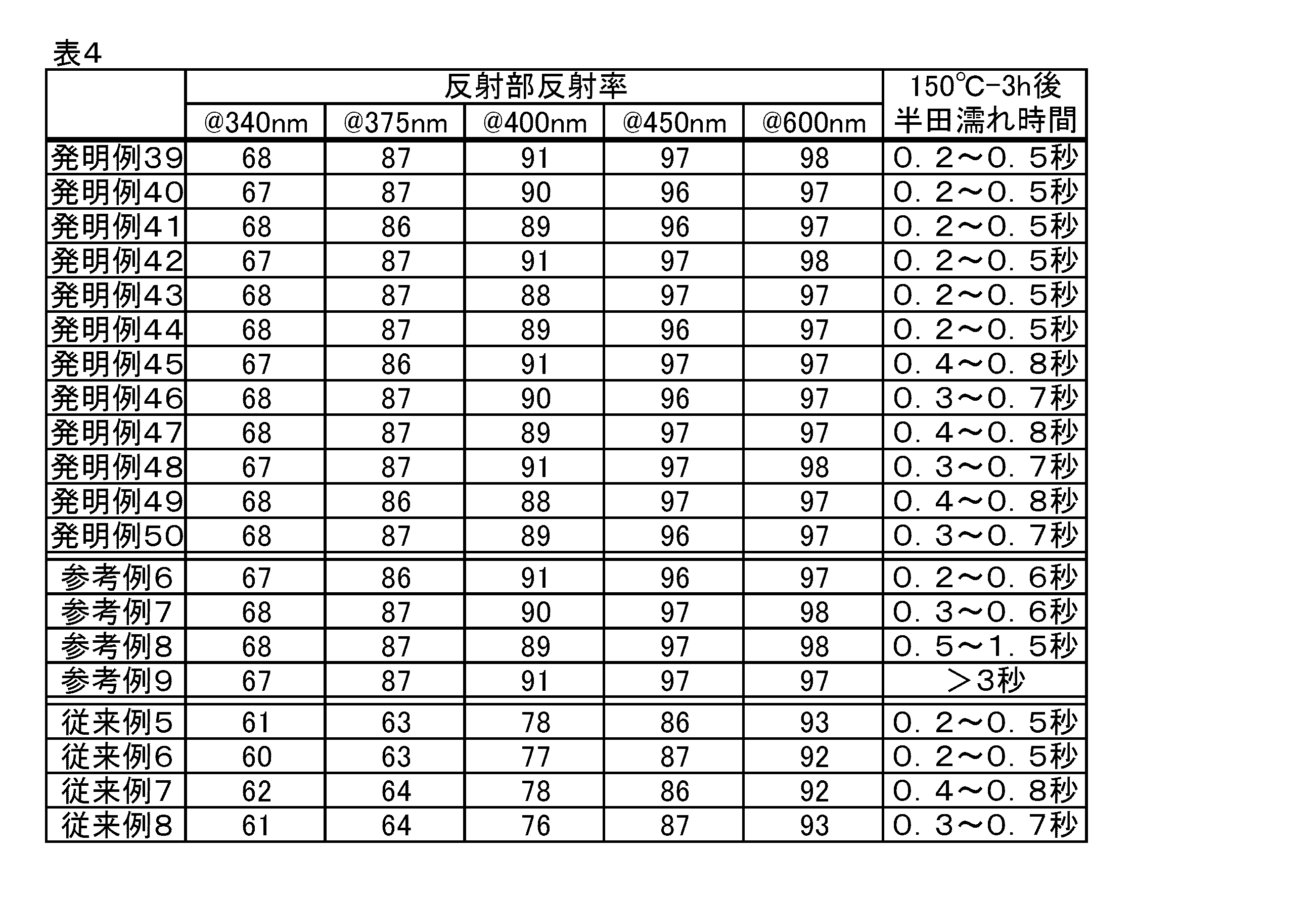
(a)めっきされたAg被覆が圧延された反射層を3μm有していれば、反射率は実施例1と同様に良好である。
(b)外部リードに半田濡れの良好なめっき皮膜としてAg、SnまたはAuをめっきした発明例は、いずれも半田付け性の問題はないことがわかった。
(c)外部リードに半田濡れの良好なめっきを施していない参考例においては、薄い板厚で広い幅では問題ないが、狭い幅では、やや濡れ時間が長い。厚い板厚で広い幅でも若干濡れ時間が長くなっており、狭い幅になるとかなり濡れ時間が長くなっている。
(d)上記(b)、(c)から、半田付けの信頼性の高度に要求される用途や、板厚・幅から半田濡れしにくい形状の場合には、外部リードへ半田濡れの良好なめっきを施すことが好ましい。
上記の実施例においては、外部リードへのめっきとして純金属(Ag、SnまたはAu)でめっきした例を示したが、これらが合金でも同様な効果を奏することは確認している。
前記のめっき組織残存率を特徴とする態様の実施例である。
実施例3として、厚さ0.25mm、幅180mmの表5に示す導電性基体に前記と同様に前処理を行った後、前記と同様に電気めっき処理を施した。その後、Agめっき層を塑性変形させるため、圧延加工またはプレス加工により加工率を変化させて本発明例101~121、参考例101のリードフレームを作製した。参考例102は、特許文献3の比較例1を、参考例103は、特許文献3の実施例2を、それぞれ模したものであり、圧延加工を行った後に240℃で4時間の熱処理を実施したものを準備した(熱処理上がり品)。また、従来例101のめっき上がり品については、板厚0.25mm、幅180mmの表5に示す導電性基体に前記と同様に前処理を行った後、前記と同様に電気めっき処理を施し、圧延を行わないで、リードフレームを作製した。また従来例102では、従来例101で得られためっき材に、残留酸素濃度500ppm以下の窒素雰囲気にて、300℃で5分間の熱処理を行ったリードフレームを準備し、結晶粒径を熱処理によって調整したものを準備した。(中間層のない実施例及び参考例が図1に示したリードフレームの構造に相当し、中間層のある実施例が図2に示したリードフレームの構造に相当する。)
[Agストライクめっき]
めっき液:KAg(CN)2 4.45g/リットル、KCN 60g/リットル
めっき条件:電流密度 5A/dm2、温度 25℃

上記のようにして得られた、表5の発明例、参考例および従来例のリードフレームについて、下記試験および基準により評価を行った。その結果を表5に示す。なお、従来例とは、比較例のうち従来技術相当のものを示す。
(3A)反射率測定:分光光度計(V660(商品名、日本分光(株)製))において、全反射率を300nm~800nmにかけて連続測定を実施した。このうち、400nm、450nm、600nmおよび800nmにおける全反射率(%)を表5に示す。それぞれ波長400nmでの反射率を85%以上、波長450nm~800nmでの反射率を90%以上であることが要求特性とした。
(3B)耐熱性:150℃の温度で3時間大気中にて熱処理を行った後、上記反射率測定を実施した。その結果、波長450nmの全反射率がまったく変化しなかったものを「AA」、反射率低下が2%以内であったものを「A」、反射率低下が2%を越え5%以内だったものを「B」、反射率低下が5%を越えたものを「C」とし、B以上を耐熱性に優れ安定な反射率が得られる実用レベルとして表5に示した。
一方の従来例101は通常の銀めっき品であるが、波長400nmの反射率が85%以下、さらに波長450nmでは反射率が85%であり、450nm発光のチップを搭載した場合、本発明例の方が5~10%も輝度が高いことを意味する。このことは、反射率向上によりこれらの波長を利用した光半導体に好適に用いられることが期待される。さらに従来例102は、銀めっき後に熱処理を施して結晶粒径を0.5μm以上に粗大化させた例であるが、初期の反射率が波長400nmでは85%を僅かながら下回っており、さらに耐熱性が劣っていることが分かる。これは、リードフレームタイプに従来例2のような熱処理を施すと、基体の銅成分が表層にまで拡散しやすくなり、その結果耐熱性に劣るものと考えられる。このため、機械的な加工によりめっき組織の少なくとも表面を変形させて本発明例では耐熱性にも優れ、反射率が熱劣化しにくい光半導体用リードフレームが提供できる。
さらに参考例101においては、銀からなる反射層のめっき組織残存率が50%を上回っており、その結果波長400nmおよび450nmの反射率がそれぞれ85%および90%を下回っていることから、反射率改善が不十分であることが分かる。
さらに参考例102、参考例103においては、銀からなる反射層のめっき組織残存率は50%を下回っているものの、圧延加工後に過剰な熱処理が加えられている。この結果、反射率の低下が大きく、全波長域で反射率の低下が見られていることから、先述の適正な熱処理条件を超えないようにすることが必要であることがわかる。
これらの結果から、最表層の銀からなる反射層を電気めっき法で形成後、そのめっき組織残存率を50%以下にすることによって、波長400nmで反射率85%以上、波長450~800nmで反射率90%以上が達成でき、本発明のリードフレームを光半導体装置に用いることで、優れた輝度を示し、かつ耐熱性に優れるので長期に渡って高輝度を維持できる、優れた光半導体装置を提供できることが分かる。
前記の表面粗さを特徴とする態様の実施例である。
実施例4として、金属基体は古河電気工業株式会社製銅基合金「EFTEC64T-C(C18045)」(商品名)を使用した。幅100mmとした。以下に示す前処理を行った後、以下に示す電気めっき処理を施すことで銀めっき層を1.0μmの厚さで形成させた。
[電解脱脂]
脱脂液:NaOH 60g/リットル
脱脂条件:2.5A/dm2、温度60℃、脱脂時間60秒
[酸洗]
酸洗液:10%硫酸
酸洗条件:30秒 浸漬、室温
[銀ストライクめっき]
めっき液:KAg(CN)2 4.45g/リットル、KCN 60g/リットル
めっき条件:電流密度 5A/dm2、温度 25℃
[銀めっき]
めっき液:AgCN 50g/リットル、KCN 100g/リットル、K2CO3 30g/リットル
めっき条件:電流密度 1A/dm2、温度 30℃
AFM(Mobile S:製品名、Nanosurf社製、触針:CONTR-10#)でミクロな表面粗さSaを測定した。視野角は6.16μm×6.16μmとした。
それぞれの波長に対する全反射率を表6に示した。連続測定の結果から、各波長間で全反射率が急落することはないことを確認している。
◎:全くハガレが無い(優)
○:端に浮きが見られる(良)
△:多少の剥離が認められる(可)
×:剥離してしまう(不可)

前記の表面粗さを特徴とする態様の実施例である。
上述のAgめっき材の評価と同様に、実施例5としてAu、Cu、Pt、Al及びRhについても同様の評価を行った。
用いた各金属めっきのめっき条件は以下の通りである。
[Auめっき]
めっき液:KAu(CN)2 14.6g/リットル、C6H8O7 150g/リットル、K2C6H4O7 180g/リットル
めっき条件:電流密度 1A/dm2、温度 40℃
[Cuめっき]
めっき液:CuSO4・5H2O 250g/リットル、H2SO4 50g/リットル、NaCl 0.1g/リットル
めっき条件:電流密度 6A/dm2、温度 40℃
[Ptめっき]
めっき液:Pt(NO2)(NH3)2 10g/リットル、NaNO2 10g/リットル、NH4NO3 100g/リットル、NH3 50ミリリットル/リットル
めっき条件:電流密度 5A/dm2、温度 80℃
[Alスパッタリング]
装置名:SPV-403(製品名、トッキ(株)製)
ターゲット:純度99.99%
スパッタ条件:スパッタレート 27nm/分、RF Power 100W、圧力 3×10⁻³torr、Ar流量 50sccm(standard cc/min、1atm(大気圧1013hPa)、25℃での流量)
[Rhめっき]
めっき液:RHODEX(商品名、日本エレクトロプレイティングエンジニヤース(株)製)
めっき条件:1.3A/dm2、温度 50℃
また、それぞれのサンプルについて、実施例4と同様に全反射率を連続して測定した。
さらに、前述の実施例4と同様に樹脂密着性の評価を行った。その評価方法は、前述の実施例4と同様である。
それらの結果を以下の表7に示す。

前記の表面粗さを特徴とする態様の実施例である。
実施例6として、前記実施例4に示したコロイダルシリカの研磨による表面の平滑化をロールの表面粗さを変えた圧延による表面の平滑化に変え、前述の実施例4と同様の評価を行った。前記Agめっき層を形成させた後に、圧延工程を通すため、マクロな表面粗さとミクロな表面粗さが同時に変化した。ここで、圧延加工率を変えることでマクロな表面粗さとミクロな表面粗さを同時に変えた。圧延に使用するロール粗度を変化させることで、ある程度ミクロな表面粗さを制御した。同じ圧延加工率においてもロール粗度が小さければミクロな表面粗さは小さくなった。
表中、圧延加工率(%)は、圧延加工前の材料の断面積と圧延加工後の断面積の差を圧延加工前の材料の断面積で割った百分率(%)で表した値である。
その結果を以下の表8に示す。

2 反射層(圧延加工された層)
3 光半導体素子
4 中間層
5 モールド樹脂
6 封止樹脂
7 ボンディングワイヤ
8 半田付け改善層(Ag、Au、Sn、それらの合金など)
Claims (20)
- 基体の最表面の、少なくとも片面もしくは両面に、一部もしくは全面に反射層を具備してなる光半導体装置用リードフレームであって、前記反射層が、少なくとも光半導体素子が発する光を反射する領域の最表面において、金属またはその合金からなるめっき組織の少なくとも表面が機械的に変形された組織を有することを特徴とする、光半導体装置用リードフレーム。
- 前記反射層が、接触針式表面粗さ計による測定での表面粗さRaが0.010μm以上であり、かつ原子間力顕微鏡による測定での表面粗さSaが50nm以下であることを特徴とする、請求項1に記載の光半導体装置用リードフレーム。
- 前記反射層が、銀(Ag)、金(Au)、銅(Cu)、プラチナ(Pt)、アルミニウム(Al)、ロジウム(Rh)のいずれか、またはそれらの合金からなることを特徴とする請求項2に記載の光半導体装置用リードフレーム。
- 前記反射層が銀からなり、その少なくとも表面において、機械的変形により残存した銀からなるめっき組織の面積比が50%以下であることを特徴とする、請求項1に記載の光半導体装置用リードフレーム。
- 前記機械的に変形された反射層の厚さが、0.2~10μmであることを特徴とする、請求項1~4のいずれか1項に記載の光半導体装置用リードフレーム。
- 前記反射層を形成する金属またはその合金が、銀、銀-錫合金、銀-インジウム合金、銀-ロジウム合金、銀-ルテニウム合金、銀-金合金、銀-パラジウム合金、銀-ニッケル合金、銀-セレン合金、銀-アンチモン合金、または銀-白金合金であることを特徴とする、請求項1または5に記載の光半導体装置用リードフレーム。
- 前記基体が、銅、銅合金、鉄、鉄合金、アルミニウム、またはアルミニウム合金からなることを特徴とする、請求項1~6のいずれか1項に記載の光半導体装置用リードフレーム。
- 前記基体が、その上に金属層をn層(nは1以上の整数)具備し、かつ前記反射層が前記基体上に、直接、または前記金属層の少なくとも1層を介して設けられていることを特徴とする請求項1~7のいずれか1項に記載の光半導体装置用リードフレーム。
- 少なくとも半田付けを要する部分に、銀、銀合金、スズ、スズ合金、金、または金合金のいずれかからなるめっき層を有してなることを特徴とする、請求項1~8のいずれか1項に記載の光半導体装置用リードフレーム。
- 請求項1~8のいずれか1項に記載の半導体装置用リードフレームの素材を製造する方法であって、基体の最表面であって少なくとも光半導体素子が発する光を反射する領域に、金属またはその合金からなる反射層をめっき法で形成した後、機械的加工を施して少なくとも前記反射層の表面のめっき組織を機械的に変形することを特徴とする、光半導体装置用リードフレーム素材の製造方法。
- 前記反射層形成後の機械的加工を、圧延加工で行い該圧延加工時の加工率を1%以上80%以下とするか、プレス加工で行い該プレス加工時の加工率を1%以上80%以下とするか、または、機械的研磨で行うことを特徴とする、請求項10に記載の光半導体装置用リードフレーム素材の製造方法。
- 請求項1~8のいずれか1項に記載の半導体装置用リードフレームを製造する方法であって、基体の最表面であって少なくとも光半導体素子が発する光を反射する領域に金属またはその合金からなる反射層をめっき法で形成した後、機械的加工を施して少なくとも前記反射層の表面のめっき組織が機械的に変形された光半導体装置用リードフレーム素材を得て、該素材にプレス法もしくはエッチング法により抜き加工を施して、リードフレームを得ることを特徴とする、光半導体装置用リードフレームの製造方法。
- 前記反射層形成後の機械的加工を、圧延加工で行い該圧延加工時の加工率を1%以上80%以下とするか、プレス加工で行い該プレス加工時の加工率を1%以上80%以下とするか、または、機械的研磨で行うことを特徴とする、請求項12に記載の光半導体装置用リードフレームの製造方法。
- 前記抜き加工後に、半田付け性の良好なめっきを部分的に施すことを特徴とする、請求項12または13項に記載の光半導体装置用リードフレームの製造方法。
- 前記半田付け性の良好なめっきは、少なくとも光半導体素子が発する光を反射する領域以外の領域に施され、前記めっきの成分は、銀、銀合金、スズ、スズ合金、金、または金合金のいずれかであることを特徴とする、請求項14に記載の光半導体装置用リードフレームの製造方法。
- 光半導体素子と、請求項1~9のいずれか1項に記載の光半導体装置用リードフレームとを具備してなる光半導体装置であって、前記光半導体装置用リードフレームの反射層が、基体の最表面であって少なくとも前記光半導体素子から発生する光を反射する領域に設けられた、かつ、少なくとも表面のめっき組織が機械的に変形された組織を有することを特徴とする光半導体装置。
- 前記光半導体素子の発光波長が340nmから800nmであることを特徴とする、請求項16に記載の光半導体装置。
- 装置から出力される光が白色光であることを特徴とする、請求項16または17に記載の光半導体装置。
- 装置から出力される光が紫外、近紫外または紫光であることを特徴とする、請求項16または17に記載の光半導体装置。
- 請求項16~19のいずれか1項に記載の光半導体装置を具備してなることを特徴とする照明装置。
Priority Applications (4)
| Application Number | Priority Date | Filing Date | Title |
|---|---|---|---|
| KR1020127021093A KR101718575B1 (ko) | 2010-06-15 | 2011-06-13 | 광반도체 장치용 리드 프레임, 광반도체 장치용 리드 프레임의 제조방법, 및 광반도체 장치 |
| CN201180019412.4A CN102844897B (zh) | 2010-06-15 | 2011-06-13 | 光半导体装置用引线框架、光半导体装置用引线框架的制造方法以及光半导体装置 |
| EP11795716.7A EP2584621A4 (en) | 2010-06-15 | 2011-06-13 | PCB FOR AN OPTICAL SEMICONDUCTOR COMPONENT, METHOD FOR PRODUCING THE PCB FOR AN OPTICAL SEMICONDUCTOR COMPONENT AND OPTICAL SEMICONDUCTOR COMPONENT |
| US13/714,000 US20130099270A1 (en) | 2010-06-15 | 2012-12-13 | Lead frame for optical semiconductor device, method of producing the same, and optical semiconductor device |
Applications Claiming Priority (6)
| Application Number | Priority Date | Filing Date | Title |
|---|---|---|---|
| JP2010-136596 | 2010-06-15 | ||
| JP2010136596 | 2010-06-15 | ||
| JP2010-142664 | 2010-06-23 | ||
| JP2010142664 | 2010-06-23 | ||
| JP2010-157132 | 2010-07-09 | ||
| JP2010157132 | 2010-07-09 |
Related Child Applications (1)
| Application Number | Title | Priority Date | Filing Date |
|---|---|---|---|
| US13/714,000 Continuation US20130099270A1 (en) | 2010-06-15 | 2012-12-13 | Lead frame for optical semiconductor device, method of producing the same, and optical semiconductor device |
Publications (1)
| Publication Number | Publication Date |
|---|---|
| WO2011158811A1 true WO2011158811A1 (ja) | 2011-12-22 |
Family
ID=45348210
Family Applications (1)
| Application Number | Title | Priority Date | Filing Date |
|---|---|---|---|
| PCT/JP2011/063542 Ceased WO2011158811A1 (ja) | 2010-06-15 | 2011-06-13 | 光半導体装置用リードフレーム、光半導体装置用リードフレームの製造方法、および光半導体装置 |
Country Status (6)
| Country | Link |
|---|---|
| US (1) | US20130099270A1 (ja) |
| EP (1) | EP2584621A4 (ja) |
| KR (1) | KR101718575B1 (ja) |
| CN (1) | CN102844897B (ja) |
| TW (1) | TWI536616B (ja) |
| WO (1) | WO2011158811A1 (ja) |
Cited By (5)
| Publication number | Priority date | Publication date | Assignee | Title |
|---|---|---|---|---|
| WO2015029211A1 (ja) * | 2013-08-30 | 2015-03-05 | 古河電気工業株式会社 | 光半導体装置用リードフレーム用の基体とその製造方法、これを用いた光半導体装置用リードフレームとその製造方法、および光半導体装置 |
| JP2015079841A (ja) * | 2013-10-16 | 2015-04-23 | 古河電気工業株式会社 | 光半導体装置用リードフレーム基体、光半導体装置用リードフレーム、および光半導体装置用リードフレームの製造方法 |
| CN105742459A (zh) * | 2012-05-18 | 2016-07-06 | 九尊城网络科技(深圳)有限公司 | 发光二极管及其封装方法 |
| JP2017005265A (ja) * | 2016-09-01 | 2017-01-05 | 大日本印刷株式会社 | 半導体装置 |
| JP2017011101A (ja) * | 2015-06-22 | 2017-01-12 | Shマテリアル株式会社 | Ledパッケージ及び多列型led用リードフレーム、並びにそれらの製造方法 |
Families Citing this family (10)
| Publication number | Priority date | Publication date | Assignee | Title |
|---|---|---|---|---|
| CN103354270B (zh) * | 2013-07-01 | 2016-08-24 | 宁波康强电子股份有限公司 | 一种emc封装led引线框架去溢料工艺 |
| JP6085536B2 (ja) * | 2013-08-05 | 2017-02-22 | 株式会社Shカッパープロダクツ | 銅条、めっき付銅条、リードフレーム及びledモジュール |
| DE102013224581A1 (de) * | 2013-11-29 | 2015-06-03 | Osram Opto Semiconductors Gmbh | Optoelektronisches Bauelement und Verfahren zu seiner Herstellung |
| US20150364626A1 (en) * | 2014-06-11 | 2015-12-17 | Electronics And Telecommunications Research Institute | Transparent electrode and solar cell including the same |
| US9859481B2 (en) | 2014-12-22 | 2018-01-02 | Nichia Corporation | Light emitting device |
| US9590158B2 (en) | 2014-12-22 | 2017-03-07 | Nichia Corporation | Light emitting device |
| JP6237826B2 (ja) * | 2015-09-30 | 2017-11-29 | 日亜化学工業株式会社 | パッケージ及び発光装置、並びにそれらの製造方法 |
| EP3618129B1 (en) * | 2017-04-27 | 2023-03-29 | KYOCERA Corporation | Circuit board and light-emitting device provided with same |
| CN110800118B (zh) * | 2017-06-29 | 2022-10-28 | 京瓷株式会社 | 电路基板以及具备该电路基板的发光装置 |
| EP4525037A4 (en) * | 2023-07-26 | 2025-05-14 | Diodes Incorporated | Semiconductor chip package and manufacturing method therefor |
Citations (12)
| Publication number | Priority date | Publication date | Assignee | Title |
|---|---|---|---|---|
| JPS61148883A (ja) | 1984-12-22 | 1986-07-07 | Toshiba Corp | 光半導体装置用リ−ドフレ−ム |
| JPS61156779A (ja) * | 1984-12-28 | 1986-07-16 | Toshiba Corp | 発光表示装置用電極部材の製造方法 |
| JP2003282948A (ja) * | 2002-03-20 | 2003-10-03 | Sharp Corp | 発光装置およびその製造方法 |
| JP3515226B2 (ja) | 1995-06-22 | 2004-04-05 | 古河電気工業株式会社 | 銀被覆バネ用りん青銅とその製造方法 |
| JP2005029849A (ja) | 2003-07-07 | 2005-02-03 | Kobe Steel Ltd | リフレクター用Ag合金反射膜、及び、このAg合金反射膜を用いたリフレクター、並びに、このAg合金反射膜の形成用のAg合金スパッタリングターゲット |
| JP2007194385A (ja) * | 2006-01-19 | 2007-08-02 | Stanley Electric Co Ltd | 半導体発光装置及び半導体発光装置の製造方法 |
| JP2008016674A (ja) | 2006-07-06 | 2008-01-24 | Matsushita Electric Works Ltd | 銀膜、銀膜の製造方法、led実装用基板、及びled実装用基板の製造方法 |
| JP2008277349A (ja) * | 2007-04-25 | 2008-11-13 | Kyocera Corp | 発光素子搭載用基体、及びその製造方法、ならびに発光装置 |
| JP2009135355A (ja) * | 2007-12-03 | 2009-06-18 | Hitachi Cable Precision Co Ltd | リードフレーム及びその製造方法並びに受発光装置 |
| JP2010136596A (ja) | 2008-12-08 | 2010-06-17 | Nippon Densan Corp | モータ |
| JP2010142664A (ja) | 2010-02-18 | 2010-07-01 | Sammy Corp | 弾球遊技機 |
| JP2010157132A (ja) | 2008-12-27 | 2010-07-15 | Incs Inc | 設計支援装置、設計支援システム、設計支援方法、コンピュータプログラム及び記録媒体 |
Family Cites Families (5)
| Publication number | Priority date | Publication date | Assignee | Title |
|---|---|---|---|---|
| JPS53122392A (en) * | 1977-03-31 | 1978-10-25 | Omron Tateisi Electronics Co | Manufacture for photo electric device |
| KR101059361B1 (ko) * | 2003-01-16 | 2011-08-24 | 파나소닉 주식회사 | 리드 프레임 및 반도체 발광장치 |
| US7425083B2 (en) * | 2005-05-02 | 2008-09-16 | Samsung Electro-Mechanics Co., Ltd. | Light emitting device package |
| JP2008288394A (ja) * | 2007-05-17 | 2008-11-27 | Sharp Corp | 金属反射壁の製造方法 |
| KR101077264B1 (ko) * | 2009-02-17 | 2011-10-27 | (주)포인트엔지니어링 | 광소자용 기판, 이를 갖는 광소자 패키지 및 이의 제조 방법 |
-
2011
- 2011-06-13 CN CN201180019412.4A patent/CN102844897B/zh not_active Expired - Fee Related
- 2011-06-13 WO PCT/JP2011/063542 patent/WO2011158811A1/ja not_active Ceased
- 2011-06-13 KR KR1020127021093A patent/KR101718575B1/ko not_active Expired - Fee Related
- 2011-06-13 EP EP11795716.7A patent/EP2584621A4/en not_active Withdrawn
- 2011-06-15 TW TW100120805A patent/TWI536616B/zh not_active IP Right Cessation
-
2012
- 2012-12-13 US US13/714,000 patent/US20130099270A1/en not_active Abandoned
Patent Citations (12)
| Publication number | Priority date | Publication date | Assignee | Title |
|---|---|---|---|---|
| JPS61148883A (ja) | 1984-12-22 | 1986-07-07 | Toshiba Corp | 光半導体装置用リ−ドフレ−ム |
| JPS61156779A (ja) * | 1984-12-28 | 1986-07-16 | Toshiba Corp | 発光表示装置用電極部材の製造方法 |
| JP3515226B2 (ja) | 1995-06-22 | 2004-04-05 | 古河電気工業株式会社 | 銀被覆バネ用りん青銅とその製造方法 |
| JP2003282948A (ja) * | 2002-03-20 | 2003-10-03 | Sharp Corp | 発光装置およびその製造方法 |
| JP2005029849A (ja) | 2003-07-07 | 2005-02-03 | Kobe Steel Ltd | リフレクター用Ag合金反射膜、及び、このAg合金反射膜を用いたリフレクター、並びに、このAg合金反射膜の形成用のAg合金スパッタリングターゲット |
| JP2007194385A (ja) * | 2006-01-19 | 2007-08-02 | Stanley Electric Co Ltd | 半導体発光装置及び半導体発光装置の製造方法 |
| JP2008016674A (ja) | 2006-07-06 | 2008-01-24 | Matsushita Electric Works Ltd | 銀膜、銀膜の製造方法、led実装用基板、及びled実装用基板の製造方法 |
| JP2008277349A (ja) * | 2007-04-25 | 2008-11-13 | Kyocera Corp | 発光素子搭載用基体、及びその製造方法、ならびに発光装置 |
| JP2009135355A (ja) * | 2007-12-03 | 2009-06-18 | Hitachi Cable Precision Co Ltd | リードフレーム及びその製造方法並びに受発光装置 |
| JP2010136596A (ja) | 2008-12-08 | 2010-06-17 | Nippon Densan Corp | モータ |
| JP2010157132A (ja) | 2008-12-27 | 2010-07-15 | Incs Inc | 設計支援装置、設計支援システム、設計支援方法、コンピュータプログラム及び記録媒体 |
| JP2010142664A (ja) | 2010-02-18 | 2010-07-01 | Sammy Corp | 弾球遊技機 |
Non-Patent Citations (1)
| Title |
|---|
| See also references of EP2584621A4 |
Cited By (5)
| Publication number | Priority date | Publication date | Assignee | Title |
|---|---|---|---|---|
| CN105742459A (zh) * | 2012-05-18 | 2016-07-06 | 九尊城网络科技(深圳)有限公司 | 发光二极管及其封装方法 |
| WO2015029211A1 (ja) * | 2013-08-30 | 2015-03-05 | 古河電気工業株式会社 | 光半導体装置用リードフレーム用の基体とその製造方法、これを用いた光半導体装置用リードフレームとその製造方法、および光半導体装置 |
| JP2015079841A (ja) * | 2013-10-16 | 2015-04-23 | 古河電気工業株式会社 | 光半導体装置用リードフレーム基体、光半導体装置用リードフレーム、および光半導体装置用リードフレームの製造方法 |
| JP2017011101A (ja) * | 2015-06-22 | 2017-01-12 | Shマテリアル株式会社 | Ledパッケージ及び多列型led用リードフレーム、並びにそれらの製造方法 |
| JP2017005265A (ja) * | 2016-09-01 | 2017-01-05 | 大日本印刷株式会社 | 半導体装置 |
Also Published As
| Publication number | Publication date |
|---|---|
| TWI536616B (zh) | 2016-06-01 |
| US20130099270A1 (en) | 2013-04-25 |
| EP2584621A1 (en) | 2013-04-24 |
| CN102844897B (zh) | 2016-01-13 |
| KR101718575B1 (ko) | 2017-03-21 |
| TW201218463A (en) | 2012-05-01 |
| EP2584621A4 (en) | 2015-12-16 |
| KR20130077811A (ko) | 2013-07-09 |
| CN102844897A (zh) | 2012-12-26 |
Similar Documents
| Publication | Publication Date | Title |
|---|---|---|
| KR101718575B1 (ko) | 광반도체 장치용 리드 프레임, 광반도체 장치용 리드 프레임의 제조방법, 및 광반도체 장치 | |
| JP4763094B2 (ja) | 光半導体装置用リードフレーム及びその製造方法 | |
| JP5089795B2 (ja) | 光半導体装置用リードフレーム、光半導体装置用リードフレームの製造方法、および光半導体装置 | |
| JP4897981B2 (ja) | 光半導体装置用リードフレーム、その製造方法および光半導体装置 | |
| JP4885309B2 (ja) | 光半導体装置用リードフレーム、光半導体装置用リードフレームの製造方法および光半導体装置 | |
| EP2448027A1 (en) | Lead frame for optical semiconductor device, process for manufacturing lead frame for optical semiconductor device, and optical semiconductor device | |
| JP5578960B2 (ja) | 光半導体装置用リードフレーム及びその製造方法 | |
| JP5950563B2 (ja) | 光半導体装置用リードフレーム、光半導体装置用リードフレームの製造方法、および光半導体装置 | |
| JP4981979B2 (ja) | 高反射率化させためっき皮膜を有するled用部品材料およびled用部品 | |
| KR101894160B1 (ko) | 광반도체장치용 리드 프레임용 기체와 그 제조방법, 이것을 이용한 광반도체장치용 리드 프레임과 그 제조방법, 및 광반도체장치 | |
| JP5995641B2 (ja) | 光半導体装置用リードフレーム、光半導体装置用リードフレームの製造方法、および光半導体装置 | |
| JP5767521B2 (ja) | 光半導体装置用リードフレーム及びその製造方法 | |
| JP5839861B2 (ja) | 光半導体装置用リードフレーム、光半導体装置用リードフレームの製造方法、および光半導体装置 | |
| JP2014204046A (ja) | 光半導体装置用リードフレームとその製造方法、および光半導体装置 | |
| JP2015079841A (ja) | 光半導体装置用リードフレーム基体、光半導体装置用リードフレーム、および光半導体装置用リードフレームの製造方法 | |
| JP2012151289A (ja) | 光半導体実装用基板、その製造方法、及び光半導体装置 | |
| JP2014072247A (ja) | 長期信頼性を有する高反射率光半導体装置用リードフレーム用基体、それを用いた光半導体装置用リードフレームとその製造方法 |
Legal Events
| Date | Code | Title | Description |
|---|---|---|---|
| WWE | Wipo information: entry into national phase |
Ref document number: 201180019412.4 Country of ref document: CN |
|
| 121 | Ep: the epo has been informed by wipo that ep was designated in this application |
Ref document number: 11795716 Country of ref document: EP Kind code of ref document: A1 |
|
| ENP | Entry into the national phase |
Ref document number: 20127021093 Country of ref document: KR Kind code of ref document: A |
|
| NENP | Non-entry into the national phase |
Ref country code: DE |
|
| REEP | Request for entry into the european phase |
Ref document number: 2011795716 Country of ref document: EP |
|
| WWE | Wipo information: entry into national phase |
Ref document number: 2011795716 Country of ref document: EP |