WO2012011223A1 - 導電性部材、プロセスカートリッジおよび電子写真装置 - Google Patents
導電性部材、プロセスカートリッジおよび電子写真装置 Download PDFInfo
- Publication number
- WO2012011223A1 WO2012011223A1 PCT/JP2011/003450 JP2011003450W WO2012011223A1 WO 2012011223 A1 WO2012011223 A1 WO 2012011223A1 JP 2011003450 W JP2011003450 W JP 2011003450W WO 2012011223 A1 WO2012011223 A1 WO 2012011223A1
- Authority
- WO
- WIPO (PCT)
- Prior art keywords
- conductive
- metal oxide
- structural formula
- oxide particles
- group
- Prior art date
- Legal status (The legal status is an assumption and is not a legal conclusion. Google has not performed a legal analysis and makes no representation as to the accuracy of the status listed.)
- Ceased
Links
Images




Classifications
-
- G—PHYSICS
- G03—PHOTOGRAPHY; CINEMATOGRAPHY; ANALOGOUS TECHNIQUES USING WAVES OTHER THAN OPTICAL WAVES; ELECTROGRAPHY; HOLOGRAPHY
- G03G—ELECTROGRAPHY; ELECTROPHOTOGRAPHY; MAGNETOGRAPHY
- G03G15/00—Apparatus for electrographic processes using a charge pattern
- G03G15/02—Apparatus for electrographic processes using a charge pattern for laying down a uniform charge, e.g. for sensitising; Corona discharge devices
-
- G—PHYSICS
- G03—PHOTOGRAPHY; CINEMATOGRAPHY; ANALOGOUS TECHNIQUES USING WAVES OTHER THAN OPTICAL WAVES; ELECTROGRAPHY; HOLOGRAPHY
- G03G—ELECTROGRAPHY; ELECTROPHOTOGRAPHY; MAGNETOGRAPHY
- G03G15/00—Apparatus for electrographic processes using a charge pattern
- G03G15/02—Apparatus for electrographic processes using a charge pattern for laying down a uniform charge, e.g. for sensitising; Corona discharge devices
- G03G15/0208—Apparatus for electrographic processes using a charge pattern for laying down a uniform charge, e.g. for sensitising; Corona discharge devices by contact, friction or induction, e.g. liquid charging apparatus
- G03G15/0216—Apparatus for electrographic processes using a charge pattern for laying down a uniform charge, e.g. for sensitising; Corona discharge devices by contact, friction or induction, e.g. liquid charging apparatus by bringing a charging member into contact with the member to be charged, e.g. roller, brush chargers
- G03G15/0233—Structure, details of the charging member, e.g. chemical composition, surface properties
-
- C—CHEMISTRY; METALLURGY
- C08—ORGANIC MACROMOLECULAR COMPOUNDS; THEIR PREPARATION OR CHEMICAL WORKING-UP; COMPOSITIONS BASED THEREON
- C08K—Use of inorganic or non-macromolecular organic substances as compounding ingredients
- C08K9/00—Use of pretreated ingredients
- C08K9/04—Ingredients treated with organic substances
-
- G—PHYSICS
- G03—PHOTOGRAPHY; CINEMATOGRAPHY; ANALOGOUS TECHNIQUES USING WAVES OTHER THAN OPTICAL WAVES; ELECTROGRAPHY; HOLOGRAPHY
- G03G—ELECTROGRAPHY; ELECTROPHOTOGRAPHY; MAGNETOGRAPHY
- G03G15/00—Apparatus for electrographic processes using a charge pattern
- G03G15/06—Apparatus for electrographic processes using a charge pattern for developing
- G03G15/08—Apparatus for electrographic processes using a charge pattern for developing using a solid developer, e.g. powder developer
-
- G—PHYSICS
- G03—PHOTOGRAPHY; CINEMATOGRAPHY; ANALOGOUS TECHNIQUES USING WAVES OTHER THAN OPTICAL WAVES; ELECTROGRAPHY; HOLOGRAPHY
- G03G—ELECTROGRAPHY; ELECTROPHOTOGRAPHY; MAGNETOGRAPHY
- G03G15/00—Apparatus for electrographic processes using a charge pattern
- G03G15/06—Apparatus for electrographic processes using a charge pattern for developing
- G03G15/08—Apparatus for electrographic processes using a charge pattern for developing using a solid developer, e.g. powder developer
- G03G15/0806—Apparatus for electrographic processes using a charge pattern for developing using a solid developer, e.g. powder developer on a donor element, e.g. belt, roller
- G03G15/0818—Apparatus for electrographic processes using a charge pattern for developing using a solid developer, e.g. powder developer on a donor element, e.g. belt, roller characterised by the structure of the donor member, e.g. surface properties
-
- G—PHYSICS
- G03—PHOTOGRAPHY; CINEMATOGRAPHY; ANALOGOUS TECHNIQUES USING WAVES OTHER THAN OPTICAL WAVES; ELECTROGRAPHY; HOLOGRAPHY
- G03G—ELECTROGRAPHY; ELECTROPHOTOGRAPHY; MAGNETOGRAPHY
- G03G21/00—Arrangements not provided for by groups G03G13/00 - G03G19/00, e.g. cleaning, elimination of residual charge
- G03G21/16—Mechanical means for facilitating the maintenance of the apparatus, e.g. modular arrangements
- G03G21/18—Mechanical means for facilitating the maintenance of the apparatus, e.g. modular arrangements using a processing cartridge, whereby the process cartridge comprises at least two image processing means in a single unit
-
- G—PHYSICS
- G03—PHOTOGRAPHY; CINEMATOGRAPHY; ANALOGOUS TECHNIQUES USING WAVES OTHER THAN OPTICAL WAVES; ELECTROGRAPHY; HOLOGRAPHY
- G03G—ELECTROGRAPHY; ELECTROPHOTOGRAPHY; MAGNETOGRAPHY
- G03G21/00—Arrangements not provided for by groups G03G13/00 - G03G19/00, e.g. cleaning, elimination of residual charge
- G03G21/16—Mechanical means for facilitating the maintenance of the apparatus, e.g. modular arrangements
- G03G21/18—Mechanical means for facilitating the maintenance of the apparatus, e.g. modular arrangements using a processing cartridge, whereby the process cartridge comprises at least two image processing means in a single unit
- G03G21/1803—Arrangements or disposition of the complete process cartridge or parts thereof
- G03G21/1814—Details of parts of process cartridge, e.g. for charging, transfer, cleaning, developing
-
- Y—GENERAL TAGGING OF NEW TECHNOLOGICAL DEVELOPMENTS; GENERAL TAGGING OF CROSS-SECTIONAL TECHNOLOGIES SPANNING OVER SEVERAL SECTIONS OF THE IPC; TECHNICAL SUBJECTS COVERED BY FORMER USPC CROSS-REFERENCE ART COLLECTIONS [XRACs] AND DIGESTS
- Y10—TECHNICAL SUBJECTS COVERED BY FORMER USPC
- Y10T—TECHNICAL SUBJECTS COVERED BY FORMER US CLASSIFICATION
- Y10T428/00—Stock material or miscellaneous articles
- Y10T428/25—Web or sheet containing structurally defined element or component and including a second component containing structurally defined particles
Definitions
- the present invention relates to a conductive member used in an electrophotographic apparatus, a process cartridge using the same, and the like.
- a conductive member typified by a conductive roller used in an electrophotographic apparatus generally has a conductive shaft core and a conductive layer provided on the outer periphery thereof.
- the conductive layer usually contains a binder resin and a conductive agent dispersed in the binder resin.
- electronic conductive agents such as conductive metal oxide particles are known as conductive agents that can lower the electrical resistance of the conductive layer relatively easily.
- the electrical resistance of a conductive layer made conductive with an electronic conductive agent may vary greatly depending on the dispersion state of the electronic conductive agent in the conductive layer.
- Patent Document 1 discloses a conductive inorganic material in which a sulfonic acid group having ionic conductivity is introduced into the surface of an inorganic powder by silane coupling treatment as an inorganic powder having low resistance and excellent uniform dispersibility in a resin. A powder is disclosed.
- the present inventors examined a conductive member provided with a conductive layer made conductive using the conductive inorganic powder according to Patent Document 1.
- the inorganic powder was excellent in dispersibility in the binder resin, and an effect of stabilizing the electric resistance of the conductive layer was recognized.
- the present invention has a conductive shaft core and a conductive layer
- the conductive layer includes a binder resin and conductive metal oxide particles dispersed in the binder resin,
- the metal oxide particles have a group represented by the following structural formula (1) on the surface, and the group represented by the structural formula (1) represents a hydrogen atom of a hydroxyl group that is a surface functional group derived from the metal oxide particles.
- a conductive member is provided which is introduced by substitution with a group represented by the following structural formula (1).
- R represents a divalent saturated hydrocarbon group having 1 to 4 carbon atoms).
- a process cartridge that includes the above-described conductive member as at least one of a charging member and a developing member, and is configured to be detachable from the main body of the electrophotographic apparatus. Furthermore, according to the present invention, there is provided an electrophotographic apparatus provided with the above conductive member as at least one of a charging member and a developing member.
- the present invention it is possible to obtain a conductive member having excellent durability in which electric resistance hardly changes even when a DC voltage is applied for a long time. Further, according to the present invention, it is possible to obtain a process cartridge and an electrophotographic apparatus that can stably provide a high-quality electrophotographic image.
- the inventors of the present invention have repeatedly studied a mechanism in which the electrical resistance of the conductive member including the conductive layer made conductive with the conductive inorganic powder according to Patent Document 1 is changed by applying a DC voltage over a long period of time. .
- an ion exchange group such as a sulfonic acid group by silane coupling treatment is one cause.
- FIG. 1 is an explanatory diagram of an action mechanism of a silane coupling reaction.
- the alkoxy group of the silane coupling agent is hydrolyzed in water, followed by dehydration condensation between silanol groups to form oligomeric siloxane.
- a part of the hydroxyl group of the generated oligomeric siloxane forms a covalent bond by dehydration condensation with the hydroxyl group on the surface of the metal oxide particle.
- sulfonic acid groups are introduced on the surface of the metal oxide.
- the oligomerized siloxane 51 is in a state of being bonded to the surface of the metal oxide particle 52 by one covalent bond. That is, it is assumed that a state in which the macromolecule is barely stopped on the surface of the metal oxide particle due to a small number of covalent bonds. Therefore, by applying a DC voltage over a long period of time, the covalent bond between the oligomerized siloxane and the metal oxide particles is cut, and the oligomerized siloxane having a sulfonic acid group is liberated, thereby changing the electrical resistance. Conceivable.
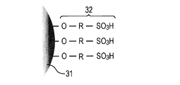
- the metal oxide particle 31 according to the present invention has an organic group 32 including a group represented by the following structural formula (1) having a relatively small size on the surface. Have. And the group shown by the said Structural formula (1) is introduce
- R represents a divalent saturated hydrocarbon group having 1 to 4 carbon atoms.
- FIG. 2 is a cross-sectional view in a direction perpendicular to the axis of the conductive roller according to the present invention. It consists of a metal core 21 as a conductive shaft core and a conductive layer 22 provided on the outer periphery thereof.
- the conductive layer 22 contains conductive metal oxide particles into which sulfonic acid groups (—SO 3 H) have been introduced, and a binder resin in which the metal oxide particles are dispersed.
- the metal oxide particle according to the present invention has a group represented by the following structural formula (1) on the surface, and this group has a hydrogen atom of a hydroxyl group that the metal oxide particle originally has as a surface functional group with the following structure. It is introduced by substitution with a group represented by the formula (1).
- R represents a divalent saturated hydrocarbon group having 1 to 4 carbon atoms).
- FIG. 3 is a schematic view showing metal oxide particles into which a sulfonic acid group has been introduced. The state where the hydrogen atom of the hydroxyl group derived from the metal oxide particle on the surface of the metal oxide particle 31 is substituted with a sulfonic acid group is shown.
- the metal oxide particles are metal oxide particles that inherently have a hydroxyl group on the surface.
- Specific examples of such metal oxide particles include particles containing oxides of Si, Mg, Al, Ti, Zr, V, Cr, Mn, Fe, Co, Ni, Cu, Sn, and Zn. More specifically, the following metal oxide particles may be mentioned.
- Spherical or needle-shaped particles such as silica, titanium oxide, aluminum oxide, alumina sol, zirconium oxide, iron oxide, chromium oxide, silicate mineral, phosphate mineral, titanate mineral, manganate mineral, niobic acid
- Layered clay minerals such as salt ore, porous titanium oxide, zeolite, mesoporous silica, porous alumina, porous silica alumina, diatomaceous earth and the like.
- the amount of hydroxyl groups on the surface of the metal oxide particles affects the ionic conductivity. Since sulfone groups are introduced by substitution with hydroxyl groups present on the surface of metal oxide particles, metal oxide particles having a larger number of hydroxyl groups on the surface are better. Examples of metal oxides having a relatively large number of hydroxyl groups on the surface include silica and titanium oxide.
- silica examples include fumed silica, colloidal silica, precipitated silica, crystalline silica, pulverized silica, and fused silica.
- titanium oxide examples include titania sol.
- Examples of layered clay minerals include silicate minerals, and specific examples include the following.
- Mica (muscovite, biotite, iron mica, phlogopite, mussel mica, soda mica, siderophyllite, eastnite, polyricio mica, triricio mica, lithia mica, chinwald mica, margarite, illite, marine stone), smectite ( Montmorillonite, beidellite, nontronite, saponite, hectorite, stevensite, talc), kaolin family (kaolinite, halloysite), vermiculite, magadiite, kanemite, kenyaite. Among these, montmorillonite, magadiite, kanemite, and kenyaite are particularly preferable.
- any metal oxide particles can be subjected to UV treatment, hydrothermal treatment, or the like, if necessary, to increase the amount of hydroxyl groups on the surface.
- shape of the metal oxide particles any shape such as a spherical shape, a rod shape, a needle shape, or a plate shape can be used. Further, it may be porous or nonporous.
- the average particle size obtained by measuring the particle size distribution of the metal oxide particles by the laser diffraction / scattering method is 50 nm or more and 500 nm or less.
- Examples of the method for introducing a sulfonic acid group onto the surface of the metal oxide particle include sulfonation using sultone, a nucleophilic substitution reaction between an alkyl halogen having a sulfonic acid group and a hydroxyl group on the surface of the metal oxide particle.
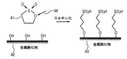
- FIG. 4 is an outline of the sulfonation reaction mechanism using sultone.
- the oxygen atom in the hydroxyl group on the surface of the metal oxide particle 42 undergoes a nucleophilic substitution reaction with respect to the carbon atom adjacent to the oxygen atom 44 of the sultone 41.
- the metal oxide particle having a sulfonic acid group on the surface can get. That is, in the sulfonation reaction with sultone, one sulfonic acid group is introduced to one hydroxyl group on the surface of the metal oxide particle, and a stable covalent bond is formed.
- an oligomer is not generated, and a sulfonic acid group can be introduced on the surface of the metal oxide particle by a one-step reaction. Furthermore, unreacted sultone is dissolved in the reaction solution, and can be removed by filtration under reduced pressure when the metal oxide particles are purified after the introduction of the sulfonic acid group. That is, even when the synthesized metal oxide particles are blended in the binder resin, impurities such as oligomers are not mixed.
- a sultone compound represented by the following structural formula (2) can be used as the sultone.
- R is a substituted or unsubstituted alkylene group having 1 to 2 carbon atoms or an unsubstituted alkenylene group having 1 to 2 carbon atoms
- A is —C (R ′) ( R ′′) — and R ′ and R ′′ each independently represent hydrogen or an alkyl group having 1 to 2 carbon atoms.
- the sultone compounds represented by the structural formula (2) include 1,3-propane sultone (A), 1,3-propene sultone (B), 1,4-butane sultone represented by the following structural formula ( C), 2,4-butane sultone (D) and the like.
- the presence or absence of oxygen atoms (-MOC-) chemically bonded to the metal M on the metal oxide surface may be confirmed.
- the presence or absence of the oxygen atom can be confirmed by combining a proton nuclear magnetic resonance ( 1 H-NMR) method and a 13 C nuclear magnetic resonance ( 13 C-NMR) method.
- the conductive layer contains a binder resin, and the conductive metal oxide particles are dispersed in the binder resin.
- a known rubber or resin can be used as the binder resin, and is not particularly limited. From the viewpoint of ionic conductivity, it is preferable to use a rubber having polarity, and examples thereof include the following. Epichlorohydrin homopolymer, epichlorohydrin-ethylene oxide copolymer, epichlorohydrin-ethylene oxide-allyl glycidyl ether terpolymer, acrylonitrile-butadiene copolymer, hydrogenated product of acrylonitrile-butadiene copolymer, acrylic rubber, urethane rubber, etc. . In addition, these 1 type may be used or 2 or more types may be used together.
- a filler, a softener, a processing aid, a crosslinking aid, a crosslinking accelerator, a crosslinking accelerator which are generally used as a rubber compounding agent, as long as they do not impair the effects of the present invention
- a crosslinking retarder, a tackifier, a dispersant, a foaming agent and the like can be added.
- the content of the metal oxide particles having a sulfonic acid group introduced as a conductive agent is 1 ⁇ 10 3 so that the volume resistivity of the conductive layer can be charged by applying a voltage.
- a guideline of the blending amount it is 0.5 to 30 parts by mass, particularly 1 to 10 parts by mass with respect to 100 parts by mass of the binder resin.
- a mixing method using a closed mixer such as a Banbury mixer or a pressure kneader, or a mixing method using an open mixer such as an open roll is used. Can be illustrated.
- the conductive member is a charging member (charging roller) or a developing member (developing roller) used in an electrophotographic image forming apparatus
- the portion of the conductive member that is in contact with the outermost photoreceptor is toner or external
- non-adhesive treatment is performed.
- the conductive member has a single-layer structure including a cored bar 21 and a conductive layer 22 provided on the outer periphery thereof. May be.
- a multilayer structure in which several intermediate layers and adhesive layers are arranged may be used.
- the outermost non-adhesive treatment there is a method of making the surface non-adhesive by irradiating the surface of the conductive member with energy rays such as electron beam, ultraviolet ray, X-ray and microwave. Further, a surface layer of a non-adhesive resin such as acrylic resin, polyurethane, polyamide, polyester, polyolefin, and silicone resin can be formed on the surface of the conductive member.
- energy rays such as electron beam, ultraviolet ray, X-ray and microwave.
- a surface layer of a non-adhesive resin such as acrylic resin, polyurethane, polyamide, polyester, polyolefin, and silicone resin can be formed on the surface of the conductive member.
- the volume resistivity is 1 ⁇ 10 3 to 1 ⁇ 10 9 ⁇ ⁇ cm.
- the volume resistivity is 1 ⁇ 10 3 to 1 ⁇ 10 9 ⁇ ⁇ cm.
- Metal oxides such as carbon black, graphite, titanium oxide and tin oxide; metals such as copper and silver; conductive particles provided with conductivity by coating the surface of the particles with oxide or metal; LiClO 4 , KSCN, NaSCN and Inorganic ionic electrolytes such as LiCF 3 SO 3 ; quaternary ammonium salts and the like.
- FIG. 8 is a schematic view of an electrophotographic apparatus using the electrophotographic conductive member of the present invention as a charging roller.
- a charging roller 302 for charging the electrophotographic photosensitive member 301, a latent image forming device 308 for performing exposure, a developing device 303 for developing the toner image, a transfer device 305 for transferring to the transfer material 304, and a transfer toner on the electrophotographic photosensitive member are collected.
- the electrophotographic photoreceptor 301 is a rotary drum type having a photosensitive layer on a conductive substrate.
- the electrophotographic photosensitive member 301 is rotationally driven in the direction of the arrow at a predetermined peripheral speed (process speed).
- the charging roller 302 is placed in contact with the electrophotographic photosensitive member 301 by being pressed with a predetermined force.
- the charging roller 302 is driven to rotate in accordance with the rotation of the electrophotographic photosensitive member 301, and applies a predetermined DC voltage from the charging power source 313 to charge the electrophotographic photosensitive member 301 to a predetermined potential.
- An electrostatic latent image is formed on the uniformly charged electrophotographic photosensitive member 301 by irradiating light 308 corresponding to image information.
- the developer 315 in the developer container 309 is supplied to the surface of the developing roller 303 disposed in contact with the electrophotographic photosensitive member 301 by the developer supply roller 311.
- the transfer device 305 has a contact-type transfer roller.
- the toner image is transferred from the electrophotographic photosensitive member 301 to a transfer material 304 such as plain paper.
- the transfer material 304 is transported by a paper feed system having a transport member.
- the cleaning device 307 includes a blade-type cleaning member and a collection container. After the transfer, the transfer residual toner remaining on the electrophotographic photosensitive member 301 is mechanically scraped and collected.
- the fixing device 306 is configured by a heated roll or the like, fixes the transferred toner image on the transfer material 304, and discharges the toner image outside the apparatus.
- Reference numerals 312 and 314 denote DC power supplies.
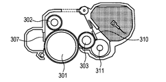
- FIG. 9 is a schematic sectional view of a process cartridge in which the electrophotographic conductive member according to the present invention is applied to the charging roller 302.
- the process cartridge is configured such that the electrophotographic photosensitive member 301, the charging roller 302, the developing device 303, the cleaning device 307, and the like are integrated, and can be attached to and detached from the main body of the electrophotographic device. ing.
- silica having a particle diameter of 100 nm (trade name: AEROSIL ⁇ 150, manufactured by AEROSIL) was prepared as a raw metal oxide particle.
- the silica was immersed in a toluene solution added with 3.0 g of 1,3-propane sultone and refluxed at 120 ° C. for 24 hours. After the reaction, the mixture was centrifuged at 10,000 rpm for 15 minutes, and the supernatant was removed and dispersed in methanol. Reprecipitation by centrifugation and washing with methanol were performed. In this way, silica having sulfonic acid groups introduced therein was synthesized.
- the content of the sulfonic acid group of the obtained silica was calculated using a Fourier transform infrared spectrophotometer (FT-IR). As a result, the sulfonic acid group content was 0.78 mmol / g.
- FT-IR Fourier transform infrared spectrophotometer
- Synthesis Example 11 Hydroxy heat treatment was performed on silica having a particle diameter of 100 nm at 170 ° C. for 24 hours using an autoclave to add hydroxyl groups to the surface.
- a silica into which a sulfonic acid group was introduced was produced in the same manner as in Synthesis Example 1 except that the silica thus obtained was used.
- the amount of sulfonic acid group introduced into the silica particles was 1.22 mmol / g.
- Synthesis Example 12 A sulfonic acid group was introduced in the same manner as in Synthesis Example 1 except that mesoporous silica having a BET specific surface area of 500 m 2 / g was used as the metal oxide particles. The content of sulfonic acid groups in the synthesized mesoporous silica was 0.84 mmol / g.
- the mesoporous silica is composed of 10.4 g of tetraethoxysilane, 5.4 g of hydrochloric acid (0.01M), 20 g of ethanol, polyethylene oxide-polypropylene oxide-polyethylene oxide terpolymer [HO (CH 2 CH 2 O) 20 ( 1.4 g of CH 2 (CH (CH 3 ) O) 70 (CH 2 CH 2 O) 20 H] (trade name: Pluronic P-123, manufactured by Aldrich) is mixed and stirred for 1 hour, and the resulting powder is recovered. Then, it synthesize
- Synthesis Example 14 A sulfonic acid group was introduced into makadiite in the same manner as in Synthesis Example 13, except that makadiite was used as the raw material metal oxide particles.
- 10 g of silica gel (Wakogel Q63, manufactured by Wako Pure Chemical Industries), 1.54 g of sodium hydroxide and 55.5 g of pure water were sealed in a sealed container made of PTFE, and makadiite was subjected to hydrothermal conditions at 150 ° C for 48 hours. The reaction was carried out under the synthesis.
- silica As raw material metal oxide particles, 10.0 g of silica with a particle size of 100 nm was prepared. The silica was immersed in a dimethylformamide solution added with 3.0 g of 2-chloroethanesulfonic acid and refluxed at 110 ° C. for 24 hours. After the reaction, the mixture was centrifuged at 10,000 rpm for 15 minutes, and the supernatant was removed and dispersed in methanol. The silica into which the sulfonic acid group was introduced was produced by repeating reprecipitation by centrifugation and washing with methanol twice.
- Example 1 A charging roller was prepared and evaluated according to the following procedure.
- GECO epichlorohydrin-ethylene oxide-allyl glycidyl ether terpolymer
- Table 4 shows the types of binder resin, the types of conductive agent, and the blending ratios thereof.
- a crosshead extruder having a core bar supply mechanism and a roller discharge mechanism is prepared.
- a die having an inner diameter of ⁇ 9.0 mm is attached to the crosshead, and the extruder and the crosshead are set to 80 ° C.
- the conveyance speed was adjusted to 60 mm / sec.
- the core metal was made of stainless steel (SUS304) and had an outer diameter of 6 mm and a total length of 258 mm. Under these conditions, an unvulcanized rubber composition was supplied from an extruder to obtain a metal core whose surface was coated with the unvulcanized rubber composition.
- the core metal coated with the unvulcanized rubber composition was put into a hot air vulcanization furnace at 170 ° C.
- a conductive elastic roller having a conductive layer formed on the outer periphery of a conductive shaft core having a diameter of 8.5 mm at the center and a diameter of 8.45 mm at a position ⁇ 90 mm from the center was manufactured.
- Methyl isobutyl ketone was added to the caprolactone-modified acrylic polyol solution to prepare a solid content of 18% by mass. Materials shown in Table 3 below were added to 100 parts by mass of the solid content of the acrylic polyol solution described above to prepare a mixed solution.
- the dipping coating dipping time is 9 seconds, and the dipping coating lifting speed is adjusted so that the initial speed is 20 mm / sec and the final speed is 2 mm / sec. Between 20 mm / sec and 2 mm / sec, the speed is linear. The speed was changed. In this way, a charging roller having a surface layer on the outer periphery of the conductive layer was produced. The charging roller thus obtained was subjected to the following test and evaluated.
- FIG. 7 shows a schematic configuration of an apparatus for measuring the electric resistance of the charging roller.
- the charging roller 71 is pressed against the cylindrical aluminum drum 73 having a diameter of 30 mm by pressing means (not shown) at both ends of the cored bar 72, and is driven to rotate as the aluminum drum 73 is driven to rotate.
- a DC voltage is applied to the cored bar portion 72 of the charging roller 71 using the external power source 74, and the voltage applied to the reference resistor 75 connected in series to the aluminum drum 73 is measured.
- the electric resistance of the charging roller 71 can be calculated by obtaining the value of the current flowing through the circuit from the measured voltage of the reference resistance 75.
- the electric resistance of the charging roller is 23.degree. C./50% humidity. H.
- measurement was performed by applying a voltage of DC 200 V between the metal core and the aluminum drum for 2 seconds using the apparatus shown in FIG. The rotational speed of the aluminum drum at this time was 30 rpm, and the resistance value of the reference resistance was 100 ⁇ .
- Data sampling was performed at a frequency of 20 Hz from 1 second to 1 second after voltage application, and the average value of the obtained electrical resistance was used as the resistance value of the charging roller.
- the initial electrical resistance value of the charging roller and the electrical resistance value after direct current flow were measured as follows. That is, using the apparatus of FIG. 7, similarly to the above-described measurement of electric resistance, a voltage of DC 200 V was applied between the metal core and the aluminum drum for 2 seconds to measure the electric resistance. The rotation speed of the aluminum drum at this time is 30 rpm, and the resistance value of the reference resistance is 100 ⁇ .
- the resistance increase rate is obtained by dividing the electrical resistance (initial value) of the charging roller before the application of the DC voltage of 200 V by the electrical resistance of the charging roller after applying the DC voltage of 200 V for 10 minutes and multiplying by 100. (%).
- Example 2 A charging roller was prepared and evaluated in the same manner as in Example 1 except that the binder resin, the conductive agent, and the amount thereof were changed as shown in Table 4.
- acrylonitrile-butadiene copolymer (trade name: Nipol DN219; manufactured by Nippon Zeon Co., Ltd.) was used as the binder resin.
- a charging roller was produced in the same manner as in Example 1 except that untreated silica particles or the conductive agent of Synthetic Example 17 was used instead of the conductive agent of Synthetic Example 1.
- Example 24 A developing roller was prepared and evaluated according to the following procedure.
- the resultant was dissolved in methyl ethyl ketone so that the total solid content ratio was 30% by mass, mixed, and then uniformly dispersed by a sand mill to obtain a coating material for forming a surface layer. Further, this paint was diluted with methyl ethyl ketone so as to have a viscosity of 10 to 13 cps, then dip coated on the conductive layer using a liquid circulation type dip coating apparatus, and then dried. Then, the developing roller which provided the surface layer about 20 micrometers in thickness on the outer periphery of the electroconductive layer was obtained by heat-processing at 150 degreeC temperature for 1 hour. The developing roller thus obtained was subjected to the following test and evaluated.
- the same electrical resistance measuring apparatus as in Example 1 was used.
- the electrical resistance of the developing roller is as follows: temperature 20 ° C./humidity 40% R.D. H. Measurement was performed by applying a voltage of 100 V DC between the cored bar and the aluminum drum for 2 seconds in an environment (also described as NN). The rotational speed of the aluminum drum at this time was 60 rpm, and the resistance value of the reference resistance was 100 ⁇ . Data sampling was performed at a frequency of 20 Hz from 1 second to 1 second after voltage application, and the average value of the obtained electrical resistance was used as the resistance value of the developing roller.
- Example 2 Further, the evaluation of the energization deterioration of the developing roller was performed in the same manner as in Example 1.
- the initial electrical resistance was measured under the above conditions.
- the rotational speed of the aluminum drum was 60 rpm
- the applied voltage between the core metal and the aluminum drum was 100 V DC
- the application time was 60 minutes.
- Examples 25 and 26 A developing roller was prepared and evaluated in the same manner as in Example 24 except that the type of conductive agent was changed as shown in Table 6.
- Example 3 A developing roller was prepared and evaluated in the same manner as in Example 24 except that untreated silica having a particle size of 100 nm was used instead of the conductive agent according to Synthesis Example 1.
- Table 6 shows the evaluation results of Examples 24 to 26 and Comparative Example 3.
Landscapes
- Physics & Mathematics (AREA)
- General Physics & Mathematics (AREA)
- Engineering & Computer Science (AREA)
- Computer Vision & Pattern Recognition (AREA)
- Plasma & Fusion (AREA)
- Chemical & Material Sciences (AREA)
- Polymers & Plastics (AREA)
- Organic Chemistry (AREA)
- Health & Medical Sciences (AREA)
- Medicinal Chemistry (AREA)
- Chemical Kinetics & Catalysis (AREA)
- Electrostatic Charge, Transfer And Separation In Electrography (AREA)
- Electrophotography Configuration And Component (AREA)
- Compositions Of Macromolecular Compounds (AREA)
- Non-Insulated Conductors (AREA)
- Dry Development In Electrophotography (AREA)
Abstract
Description
特許文献1には、低抵抗で、樹脂への均一分散性に優れた無機粉末として、無機粉末の表面に、イオン導電性を有するスルホン酸基をシランカップリング処理にて導入した導電性の無機粉末が開示されている。
該導電層は、バインダー樹脂と該バインダー樹脂中に分散されている導電性の金属酸化物粒子とを含み、
該金属酸化物粒子は下記構造式(1)で示される基を表面に有し、該構造式(1)で示される基は、金属酸化物粒子由来の表面官能基である水酸基の水素原子を下記構造式(1)で示される基で置換することによって導入されてなるものである導電性部材が提供される。
-R-SO3H 構造式(1)
-R-SO3H 構造式(1)
そのため、長期に亘る直流電圧の印加によっても金属酸化物粒子からスルホン酸基が遊離しにくく、その結果として、かかる金属酸化物粒子で導電化された導電層は、電気抵抗の経時的な変化が少なくなるものと推定される。
本発明に係る金属酸化物粒子は、表面に下記構造式(1)で示される基を有しており、この基は、金属酸化物粒子が本来表面官能基として有する水酸基の水素原子を下記構造式(1)で示される基で置換することで導入されてなるものである。
-R-SO3H 構造式(1)
本発明に係る金属酸化物粒子の製造方法について述べる。


本発明において導電層は、バインダー樹脂を含み、このバインダー樹脂に前記導電性の金属酸化物粒子が分散されている。バインダー樹脂としては、公知のゴムまたは樹脂を使用することができ、特に限定されない。イオン導電性の観点から極性を有するゴムを使用することが好ましく、例えば、以下のものが挙げられる。エピクロルヒドリンホモポリマー、エピクロルヒドリン-エチレンオキサイド共重合体、エピクロルヒドリン-エチレンオキサイド-アリルグリシジルエーテル3元共重合体、アクリロニトリル-ブタジエン共重合体、アクリロニトリル-ブタジエン共重合体の水素添加物、アクリルゴム及びウレタンゴム等。なお、これらの1種を用いても2種以上を併用してもよい。
図8は、本発明の電子写真用導電性部材を帯電ローラとして用いた電子写真装置の概略図である。電子写真感光体301を帯電する帯電ローラ302、露光を行う潜像形成装置308、トナー像に現像する現像装置303、転写材304に転写する転写装置305、電子写真感光体上の転写トナーを回収するクリーニング装置307、トナー像を定着する定着装置306などから構成される。電子写真感光体301は、導電性基体上に感光層を有する回転ドラム型である。電子写真感光体301は矢印の方向に所定の周速度(プロセススピード)で回転駆動される。
(プロセスカートリッジ)
本発明に係る導電剤である、スルホン酸基が導入された金属酸化物粒子の合成例1~16および比較例2に用いる導電剤の合成例17を以下に示す。
原料の金属酸化物粒子として粒径100nmのシリカ(商品名:AEROSIL・150、AEROSIL社製)10.0gを用意した。1,3-プロパンスルトン3.0gを添加したトルエン溶液中に上記シリカを浸漬し、120℃で24時間還流した。反応後、10000rpmで15分間遠心分離を行い、上澄み液を除去後、メタノール中に分散させた。遠心分離による再沈殿とメタノールによる洗浄を行った。こうして、スルホン酸基が導入されたシリカを合成した。得られたシリカのスルホン酸基の含有量を、フーリエ変換型赤外分光光度計(FT-IR)を用いて算出した。その結果、スルホン酸基の含有量は、0.78mmol/gであった。
表1に示す金属酸化物粒子及びスルトンを用いた以外は合成例1と同様にして、スルホン酸基が導入された金属酸化物粒子を作成した。得られた金属酸化物粒子の各々のスルホン酸基の含有量を表1に示す。
粒径100nmのシリカに対し、オートクレーブを用いて170℃で24時間の水熱処理を行い表面に水酸基を付加した。これにより得られたシリカを用いた以外は、合成例1と同様にしてスルホン酸基が導入されたシリカを作製した。シリカ粒子に導入されたスルホン酸基の量は、1.22mmol/gであった。
金属酸化物粒子として、BET比表面積が500m2/gのメソポーラスシリカを用いた以外は、合成例1と同様にして、スルホン酸基を導入した。合成したメソポーラスシリカのスルホン酸基の含有量は、0.84mmol/gであった。なお、メソポーラスシリカは、テトラエトキシシラン10.4g、塩酸(0.01M)5.4g、エタノール20g、ポリエチレンオキサイド-ポリプロピレンオキサイド-ポリエチレンオキサイド3元共重合体[HO(CH2CH2O)20(CH2(CH(CH3)O)70(CH2CH2O)20H](商品名:Pluronic P-123、Aldrich社製)1.4gを1時間混合攪拌し、得られた粉末を回収後、400℃、4時間焼成することで合成した。
原料の金属酸化物粒子として、山形県の月布鉱山から産出されたモンモリロナイト10.0g、セチルトリメチルアンモニウム10.4gを500mlの水中で24時間攪拌した。反応後、10000rpmで15分間遠心分離を行い、上澄み液を除去後、メタノール中に分散させた。遠心分離による再沈殿とメタノールによる洗浄を行うことで、層間のナトリウムイオンをセチルトリメチルアンモニウムで置換した疎水性モンモリロナイトを作製した。
原料の金属酸化物粒子として、マカディアイトを用いた以外は、合成例13と同様にしてマカディアイトにスルホン酸基を導入した。なお、マカディアイトは、シリカゲル(ワコーゲルQ63,和光純薬工業製)10g、水酸化ナトリウム1.54gと純水55.5gをPTFE製の密閉容器に封入し、150℃で48時間、水熱条件下で反応させ合成した。
原料の金属酸化物粒子として、針状酸化チタン(商品名:MT-100T、テイカ社製)(繊維径0.05~0.15μm、繊維長3~12μm)を用いた以外は、合成例1と同様にして、針状酸化チタンにスルホン酸基を導入した。
原料の金属酸化物粒子として、粒径100nmのシリカ10.0gを用意した。2-クロロエタンスルホン酸3.0gを添加したジメチルホルムアミド溶液中に、上記シリカを浸漬し、110℃で24時間還流した。反応後、10000rpmで15分間遠心分離を行い、上澄み液を除去後、メタノール中に分散させた。遠心分離による再沈殿とメタノールによる洗浄を2回繰り返すことで、スルホン酸基が導入されたシリカを作製した。
水1.8ml、35%塩酸100μl、エタノール10mlの混合溶液中にメルカプトプロピルトリメトキシシラン2mlを徐々に滴下し、50℃で1時間攪拌した。次に、原料の金属酸化物粒子としての粒径100nmのシリカ10.0gをエタノール中に分散させた溶液と混合し、70℃で13時間攪拌した。合成したメルカプト基を有するシリカ10.0gをエタノール40mlと過酸化水素水10mlの混合溶液中、70℃で2時間攪拌することにより、メルカプト基をスルホン酸基に置換し、スルホン酸基が導入されたシリカを作製した。

以下の手順で帯電ローラを作製し、評価した。
バインダー樹脂として、エピクロルヒドリン-エチレンオキサイド-アリルグリシジルエーテル3元共重合体(以下「GECO」と略す。)(商品名:エピクロマーCG-102;ダイソー社製)を用いて、表2に示す種類と量の各材料を用意した。

次に、芯金の供給機構、ローラの排出機構を有するクロスヘッド押出機を用意し、クロスヘッドには内径がφ9.0mmのダイスを取り付け、押出機とクロスヘッドを80℃に、芯金の搬送速度を60mm/secに調整した。芯金は、ステンレス製(SUS304)で外径6mm、全長258mmであった。この条件で、押出機より未加硫ゴム組成物を供給して、未加硫ゴム組成物によって表面が被覆された芯金を得た。次に、170℃の熱風加硫炉中に未加硫ゴム組成物が被覆された芯金を投入し、60分間加熱した。その後、導電層の長さが228mmになるように導電層の端部を切断・除去した。最後に、導電層の表面を回転砥石で研磨した。これによって、中央部直径8.5mm、中央部から±90mm位置の直径8.45mmの、導電性の軸芯体の外周に導電層が形成された導電性弾性ローラを作製した。
カプロラクトン変性アクリルポリオール溶液にメチルイソブチルケトンを加え、固形分が18質量%となるように調製した。前述のアクリルポリオール溶液の固形分100質量部に対して下記表3に示す材料を加えて混合溶液を調製した。

図7に、帯電ローラの電気抵抗を測定する装置の概略構成を示した。帯電ローラ71は、芯金72の両端部を不図示の押圧手段で直径30mmの円柱状のアルミドラム73に圧接されており、アルミドラム73の回転駆動に伴って従動回転する。この状態で、帯電ローラ71の芯金部分72に、外部電源74を用いて直流電圧を印加し、アルミドラム73に直列に接続した基準抵抗75にかかる電圧を測定する。帯電ローラ71の電気抵抗は、測定された基準抵抗75の電圧から、回路に流れる電流値を求めることによって算出することができる。
バインダー樹脂、導電剤およびその量を表4に示したように変更した以外は実施例1と同様に帯電ローラを作製し、評価した。なお、実施例8においては、バインダー樹脂としてアクリロニトリル-ブタジエン共重合体(NBR)(商品名:Nipol DN219;日本ゼオン社製)を用いた。
合成例1の導電剤の代わりに未処理のシリカ粒子または合成例17の導電剤を用いた以外は、実施例1と同様にして、帯電ローラを作製した。

以下の手順で現像ローラを作製し、評価した。
表2に示す各材料をオープンロールにて混合し、未加硫ゴム組成物を得た。なお、バインダー樹脂の種類、導電剤の種類、並びにこれらの配合割合を表6に示す。
次に、クロスヘッド押出機を用いて、実施例1と同様にして、直径12mmの導電性の軸芯体の外周に導電層が形成された現像ローラを作製した。
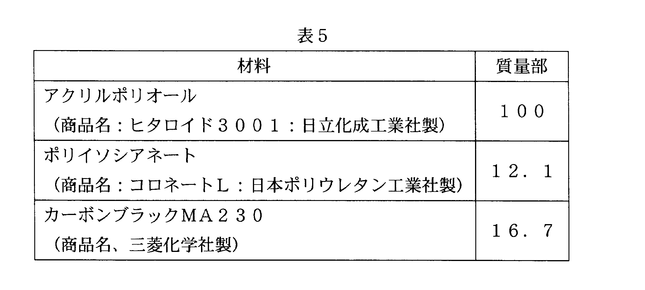
表面層の材料として下記表5に示した材料を混合撹拌した。
実施例1と同様の電気抵抗測定装置を用いた。現像ローラの電気抵抗は、温度20℃/湿度40%R.H.(NNとも記載する)環境下で、芯金とアルミドラムの間に直流100Vの電圧を2秒印加することで測定した。このときのアルミドラムの回転数は60rpm、基準抵抗の抵抗値は100Ωであった。データのサンプリングは、電圧印加後1秒後から1秒間に周波数20Hzで行い、得られた電気抵抗の平均値を、現像ローラの抵抗値とした。
導電剤の種類を表6のように変更した以外は実施例24と同様にして現像ローラを作製し、評価した。
合成例1に係る導電剤に代えて、未処理の粒径100nmのシリカを用いた以外は、実施例24と同様にして現像ローラを作製し、評価した。

22 導電層
31 金属酸化物粒子
32 スルホン酸基を含む有機鎖
41 スルトン
42 水酸基をもつ金属酸化物粒子表面
43 スルホン酸基を導入した金属酸化物粒子表面
44 酸素原子
51 スルホン酸基を含む有機基
52 金属酸化物粒子
61 金属酸化物表面との結合部に酸素原子を含む有機基
71 帯電ローラ
72 芯金
73 アルミドラム
74 外部電源
75 基準抵抗
Claims (5)
- 導電性の軸芯体と導電層とを有している導電性部材であって、
該導電層は、バインダー樹脂と該バインダー樹脂中に分散されている導電性の金属酸化物粒子とを含み、
該金属酸化物粒子は下記構造式(1)で示される基を表面に有し、該構造式(1)で示される基は、金属酸化物粒子由来の表面官能基である水酸基の水素原子を、下記構造式(1)で示される基で置換することによって導入されてなるものであることを特徴とする導電性部材:
(化6)
-R-SO3H 構造式(1)
(上記構造式(1)中、Rは、炭素数1~4の2価の飽和炭化水素基を示す)。 - 前記構造式(1)で示される基が、前記水酸基とスルトンとの反応によって導入されたものである請求項1に記載の導電性部材。
- 前記スルトンが下記構造式(2)で示される請求項2に記載の導電性部材。

- 請求項1乃至3の何れか一項に記載の導電性部材を帯電部材および現像部材の少なくとも一方として備え、かつ、電子写真装置の本体に着脱可能に構成されていることを特徴とするプロセスカートリッジ。
- 請求項1乃至3の何れか一項に記載の導電性部材を帯電部材および現像部材の少なくとも一方として備えていることを特徴とする電子写真装置。
Priority Applications (4)
| Application Number | Priority Date | Filing Date | Title |
|---|---|---|---|
| EP11809402.8A EP2597523B1 (en) | 2010-07-20 | 2011-06-16 | Conductive member, process cartridge, and electrophotographic device |
| CN201180035205.8A CN103003756B (zh) | 2010-07-20 | 2011-06-16 | 导电性构件、处理盒和电子照相设备 |
| KR1020137003379A KR101454130B1 (ko) | 2010-07-20 | 2011-06-16 | 도전성 부재, 프로세스 카트리지 및 전자 사진 장치 |
| US13/305,262 US8449975B2 (en) | 2010-07-20 | 2011-11-28 | Electroconductive member, process cartridge and electrophotographic apparatus |
Applications Claiming Priority (2)
| Application Number | Priority Date | Filing Date | Title |
|---|---|---|---|
| JP2010-163022 | 2010-07-20 | ||
| JP2010163022 | 2010-07-20 |
Related Child Applications (1)
| Application Number | Title | Priority Date | Filing Date |
|---|---|---|---|
| US13/305,262 Continuation US8449975B2 (en) | 2010-07-20 | 2011-11-28 | Electroconductive member, process cartridge and electrophotographic apparatus |
Publications (1)
| Publication Number | Publication Date |
|---|---|
| WO2012011223A1 true WO2012011223A1 (ja) | 2012-01-26 |
Family
ID=45496661
Family Applications (1)
| Application Number | Title | Priority Date | Filing Date |
|---|---|---|---|
| PCT/JP2011/003450 Ceased WO2012011223A1 (ja) | 2010-07-20 | 2011-06-16 | 導電性部材、プロセスカートリッジおよび電子写真装置 |
Country Status (6)
| Country | Link |
|---|---|
| US (1) | US8449975B2 (ja) |
| EP (1) | EP2597523B1 (ja) |
| JP (1) | JP4948664B2 (ja) |
| KR (1) | KR101454130B1 (ja) |
| CN (1) | CN103003756B (ja) |
| WO (1) | WO2012011223A1 (ja) |
Cited By (1)
| Publication number | Priority date | Publication date | Assignee | Title |
|---|---|---|---|---|
| JP2012194334A (ja) * | 2011-03-16 | 2012-10-11 | Canon Inc | 電子写真用の導電性部材 |
Families Citing this family (49)
| Publication number | Priority date | Publication date | Assignee | Title |
|---|---|---|---|---|
| JP5875416B2 (ja) | 2011-03-22 | 2016-03-02 | キヤノン株式会社 | 電子写真用導電性部材 |
| JP6000580B2 (ja) | 2011-03-29 | 2016-09-28 | キヤノン株式会社 | 接触帯電ローラ、現像部材、導電性部材およびこれらの製造方法、プロセスカートリッジならびに電子写真装置 |
| JP5893432B2 (ja) | 2011-03-30 | 2016-03-23 | キヤノン株式会社 | イオン導電性樹脂、および電子写真用導電性部材 |
| JP5972150B2 (ja) | 2011-12-19 | 2016-08-17 | キヤノン株式会社 | 電子写真用導電性部材、プロセスカートリッジおよび電子写真画像形成装置 |
| CN104011602B (zh) | 2011-12-22 | 2016-08-17 | 佳能株式会社 | 导电性构件、处理盒和电子照相设备 |
| JP5693441B2 (ja) * | 2011-12-26 | 2015-04-01 | キヤノン株式会社 | 電子写真用導電性部材、プロセスカートリッジおよび電子写真装置 |
| JP6249674B2 (ja) * | 2013-08-13 | 2017-12-20 | 東ソー株式会社 | シリカ粉末の固化方法および高純度シリカ固化体 |
| JP6231326B2 (ja) * | 2013-08-13 | 2017-11-15 | 東ソー株式会社 | シリカ固化体の製造方法およびシリカ固化体 |
| CN105579913B (zh) | 2013-09-27 | 2018-02-16 | 佳能株式会社 | 电子照相用导电性构件、处理盒和电子照相设备 |
| JP6281762B2 (ja) * | 2013-12-10 | 2018-02-21 | 住友電工プリントサーキット株式会社 | プリント配線板 |
| CN106687869B (zh) | 2014-09-10 | 2019-04-16 | 佳能株式会社 | 电子照相用导电性构件和季铵盐 |
| US9625838B2 (en) | 2014-11-28 | 2017-04-18 | Canon Kabushiki Kaisha | Electrophotographic apparatus, process cartridge, and image forming method |
| US9529284B2 (en) | 2014-11-28 | 2016-12-27 | Canon Kabushiki Kaisha | Process cartridge, image forming method, and electrophotographic apparatus |
| US9568846B2 (en) * | 2014-11-28 | 2017-02-14 | Canon Kabushiki Kaisha | Electrophotographic photosensitive member, method for producing the same, process cartridge, and electrophotographic apparatus |
| US9429864B1 (en) * | 2015-03-26 | 2016-08-30 | Fuji Xerox Co., Ltd. | Charging member, process cartridge, and image forming apparatus |
| JP6706101B2 (ja) | 2015-03-27 | 2020-06-03 | キヤノン株式会社 | 電子写真用の導電性部材、プロセスカートリッジおよび電子写真装置 |
| JP2017062322A (ja) * | 2015-09-24 | 2017-03-30 | 富士ゼロックス株式会社 | 帯電部材、帯電装置、プロセスカートリッジ及び画像形成装置 |
| US9740133B2 (en) | 2015-09-30 | 2017-08-22 | Canon Kabushiki Kaisha | Charging member, process cartridge and electrophotographic image forming apparatus |
| US10678158B2 (en) | 2016-09-26 | 2020-06-09 | Canon Kabushiki Kaisha | Electro-conductive member for electrophotography, process cartridge, and electrophotographic image forming apparatus |
| JP6976774B2 (ja) | 2016-09-27 | 2021-12-08 | キヤノン株式会社 | 電子写真用導電性部材、プロセスカートリッジおよび電子写真画像形成装置 |
| US10416588B2 (en) | 2016-10-31 | 2019-09-17 | Canon Kabushiki Kaisha | Charging member, process cartridge, electrophotographic image forming apparatus, and method for manufacturing charging member |
| WO2019203238A1 (ja) | 2018-04-18 | 2019-10-24 | キヤノン株式会社 | 導電性部材及びその製造方法、プロセスカートリッジ並びに電子写真画像形成装置 |
| WO2019203227A1 (ja) | 2018-04-18 | 2019-10-24 | キヤノン株式会社 | 導電性部材、プロセスカートリッジ、および画像形成装置 |
| CN112005173B (zh) | 2018-04-18 | 2023-03-24 | 佳能株式会社 | 导电性构件、处理盒和图像形成设备 |
| CN111989622B (zh) | 2018-04-18 | 2022-11-11 | 佳能株式会社 | 显影构件、处理盒和电子照相设备 |
| JP7336289B2 (ja) | 2018-07-31 | 2023-08-31 | キヤノン株式会社 | 電子写真用部材、電子写真プロセスカートリッジ及び電子写真画像形成装置 |
| JP7114409B2 (ja) | 2018-08-31 | 2022-08-08 | キヤノン株式会社 | 現像ローラ、電子写真プロセスカートリッジおよび電子写真画像形成装置 |
| US11169454B2 (en) | 2019-03-29 | 2021-11-09 | Canon Kabushiki Kaisha | Electrophotographic electro-conductive member, process cartridge, and electrophotographic image forming apparatus |
| JP7446878B2 (ja) | 2019-03-29 | 2024-03-11 | キヤノン株式会社 | 導電性部材、電子写真用プロセスカートリッジ、及び電子写真画像形成装置 |
| CN114556230B (zh) | 2019-10-18 | 2024-03-08 | 佳能株式会社 | 电子照相用导电性构件、处理盒和电子照相图像形成装置 |
| JP7337651B2 (ja) | 2019-10-18 | 2023-09-04 | キヤノン株式会社 | プロセスカートリッジ及び電子写真装置 |
| JP7330851B2 (ja) | 2019-10-18 | 2023-08-22 | キヤノン株式会社 | 電子写真装置、プロセスカートリッジ、及びカートリッジセット |
| JP7336351B2 (ja) | 2019-10-18 | 2023-08-31 | キヤノン株式会社 | 電子写真装置、プロセスカートリッジ、及びカートリッジセット |
| WO2021075441A1 (ja) | 2019-10-18 | 2021-04-22 | キヤノン株式会社 | 導電性部材、プロセスカートリッジ及び電子写真画像形成装置 |
| JP7669134B2 (ja) | 2019-10-18 | 2025-04-28 | キヤノン株式会社 | 導電性部材、プロセスカートリッジ並びに電子写真画像形成装置 |
| JP7330852B2 (ja) | 2019-10-18 | 2023-08-22 | キヤノン株式会社 | 電子写真装置、プロセスカートリッジ、及びカートリッジセット |
| CN114556231B (zh) | 2019-10-18 | 2023-06-27 | 佳能株式会社 | 导电性构件、其制造方法、处理盒以及电子照相图像形成设备 |
| JP7401256B2 (ja) | 2019-10-18 | 2023-12-19 | キヤノン株式会社 | 電子写真装置、プロセスカートリッジ及びカートリッジセット |
| US11112719B2 (en) | 2019-10-18 | 2021-09-07 | Canon Kabushiki Kaisha | Process cartridge and electrophotographic apparatus capable of suppressing lateral running while maintaining satisfactory potential function |
| JP7321884B2 (ja) | 2019-10-18 | 2023-08-07 | キヤノン株式会社 | 電子写真装置、プロセスカートリッジ及びカートリッジセット |
| JP7401255B2 (ja) | 2019-10-18 | 2023-12-19 | キヤノン株式会社 | 電子写真装置、プロセスカートリッジ、及びカートリッジセット |
| JP7404026B2 (ja) | 2019-10-18 | 2023-12-25 | キヤノン株式会社 | 電子写真装置、プロセスカートリッジ、及びカートリッジセット |
| JP7337649B2 (ja) | 2019-10-18 | 2023-09-04 | キヤノン株式会社 | プロセスカートリッジ及び電子写真装置 |
| JP7337650B2 (ja) | 2019-10-18 | 2023-09-04 | キヤノン株式会社 | プロセスカートリッジおよび電子写真装置 |
| JP7337652B2 (ja) | 2019-10-18 | 2023-09-04 | キヤノン株式会社 | プロセスカートリッジ及びそれを用いた電子写真装置 |
| JP2023157527A (ja) | 2022-04-15 | 2023-10-26 | キヤノン株式会社 | 電子写真用ローラ、プロセスカートリッジ及び電子写真画像形成装置 |
| CN115150323B (zh) * | 2022-07-04 | 2023-06-02 | 中国联合网络通信集团有限公司 | 路由实现方法、vtep、第一边缘设备及系统 |
| JP2025030522A (ja) | 2023-08-23 | 2025-03-07 | キヤノン株式会社 | 電子写真ローラ、現像装置、電子写真画像形成装置及びプロセスカートリッジ |
| JP2025030521A (ja) | 2023-08-23 | 2025-03-07 | キヤノン株式会社 | 電子写真ローラ、現像装置、電子写真画像形成装置及びプロセスカートリッジ |
Citations (5)
| Publication number | Priority date | Publication date | Assignee | Title |
|---|---|---|---|---|
| JPH107932A (ja) | 1996-06-28 | 1998-01-13 | Mitsubishi Materials Corp | 低抵抗の無機粉末 |
| JP2004235111A (ja) * | 2003-01-31 | 2004-08-19 | Ebara Corp | イオン伝導体及びその製造方法 |
| JP2008004533A (ja) * | 2006-05-22 | 2008-01-10 | Nissan Motor Co Ltd | イオン伝導体 |
| JP2009214051A (ja) * | 2008-03-11 | 2009-09-24 | Tokyo Univ Of Science | ダイヤモンド固体酸及び当該ダイヤモンド固体酸からなる固体酸触媒、固体電解質 |
| JP2010139832A (ja) * | 2008-12-12 | 2010-06-24 | Ricoh Co Ltd | 半導電性部材及びそれを有する現像ロール、帯電ロール、転写ベルト |
Family Cites Families (9)
| Publication number | Priority date | Publication date | Assignee | Title |
|---|---|---|---|---|
| JP3913306B2 (ja) | 1997-01-21 | 2007-05-09 | キヤノン株式会社 | 太陽電池モジュール |
| JP2004347722A (ja) | 2003-05-20 | 2004-12-09 | Fuji Photo Film Co Ltd | 記録材料用支持体及びその製造方法並びに記録材料 |
| US20060083962A1 (en) * | 2004-10-20 | 2006-04-20 | Nissan Motor Co., Ltd. | Proton-conductive composite electrolyte membrane and producing method thereof |
| JP5041695B2 (ja) * | 2005-10-14 | 2012-10-03 | 日揮触媒化成株式会社 | 帯電防止膜形成用組成物 |
| JP2008096527A (ja) * | 2006-10-06 | 2008-04-24 | Fuji Xerox Co Ltd | 電子写真感光体、画像形成装置及びプロセスカートリッジ |
| JP5147510B2 (ja) | 2007-04-27 | 2013-02-20 | キヤノン株式会社 | 電子写真用ローラ部材の製造方法 |
| JP5409282B2 (ja) * | 2009-11-10 | 2014-02-05 | キヤノン株式会社 | 電子写真感光体、該電子写真感光体を用いたプロセスカートリッジ及び電子写真装置 |
| WO2012001881A1 (ja) | 2010-06-30 | 2012-01-05 | キヤノン株式会社 | 導電部材、プロセスカートリッジおよび電子写真画像形成装置 |
| KR101454128B1 (ko) | 2010-07-13 | 2014-10-22 | 캐논 가부시끼가이샤 | 전자 사진용 도전성 부재, 프로세스 카트리지 및 전자 사진 장치 |
-
2011
- 2011-06-16 CN CN201180035205.8A patent/CN103003756B/zh active Active
- 2011-06-16 KR KR1020137003379A patent/KR101454130B1/ko not_active Expired - Fee Related
- 2011-06-16 WO PCT/JP2011/003450 patent/WO2012011223A1/ja not_active Ceased
- 2011-06-16 EP EP11809402.8A patent/EP2597523B1/en not_active Not-in-force
- 2011-07-13 JP JP2011154762A patent/JP4948664B2/ja not_active Expired - Fee Related
- 2011-11-28 US US13/305,262 patent/US8449975B2/en not_active Expired - Fee Related
Patent Citations (5)
| Publication number | Priority date | Publication date | Assignee | Title |
|---|---|---|---|---|
| JPH107932A (ja) | 1996-06-28 | 1998-01-13 | Mitsubishi Materials Corp | 低抵抗の無機粉末 |
| JP2004235111A (ja) * | 2003-01-31 | 2004-08-19 | Ebara Corp | イオン伝導体及びその製造方法 |
| JP2008004533A (ja) * | 2006-05-22 | 2008-01-10 | Nissan Motor Co Ltd | イオン伝導体 |
| JP2009214051A (ja) * | 2008-03-11 | 2009-09-24 | Tokyo Univ Of Science | ダイヤモンド固体酸及び当該ダイヤモンド固体酸からなる固体酸触媒、固体電解質 |
| JP2010139832A (ja) * | 2008-12-12 | 2010-06-24 | Ricoh Co Ltd | 半導電性部材及びそれを有する現像ロール、帯電ロール、転写ベルト |
Non-Patent Citations (1)
| Title |
|---|
| See also references of EP2597523A4 |
Cited By (1)
| Publication number | Priority date | Publication date | Assignee | Title |
|---|---|---|---|---|
| JP2012194334A (ja) * | 2011-03-16 | 2012-10-11 | Canon Inc | 電子写真用の導電性部材 |
Also Published As
| Publication number | Publication date |
|---|---|
| KR20130056282A (ko) | 2013-05-29 |
| EP2597523A1 (en) | 2013-05-29 |
| EP2597523B1 (en) | 2017-03-08 |
| CN103003756A (zh) | 2013-03-27 |
| US20120070188A1 (en) | 2012-03-22 |
| JP4948664B2 (ja) | 2012-06-06 |
| CN103003756B (zh) | 2015-06-10 |
| KR101454130B1 (ko) | 2014-10-22 |
| JP2012042935A (ja) | 2012-03-01 |
| US8449975B2 (en) | 2013-05-28 |
| EP2597523A4 (en) | 2014-06-25 |
Similar Documents
| Publication | Publication Date | Title |
|---|---|---|
| JP4948664B2 (ja) | 導電性部材、プロセスカートリッジおよび電子写真装置 | |
| JP4942232B2 (ja) | 導電部材、プロセスカートリッジおよび電子写真画像形成装置 | |
| JP5875416B2 (ja) | 電子写真用導電性部材 | |
| JP7337648B2 (ja) | プロセスカートリッジ及び画像形成装置 | |
| CN103154827B (zh) | 充电构件、处理盒和电子照相设备 | |
| CN103080848B (zh) | 充电构件、其生产方法、处理盒和电子照相设备 | |
| WO2010050616A1 (ja) | 帯電ローラ、プロセスカートリッジ及び電子写真装置 | |
| JP6370287B2 (ja) | 帯電部材、プロセスカートリッジ及び電子写真装置 | |
| CN104871092B (zh) | 电子照相用构件、处理盒和电子照相设备 | |
| Ni et al. | Preparation and characterization of silanized TiO2 nanoparticles and their application in toner | |
| CN103109241A (zh) | 充电构件、处理盒和电子照相设备 | |
| JP5717484B2 (ja) | 電子写真用の導電性部材 | |
| JP2006154634A (ja) | 電子写真用半導電性弾性部材、プロセスカートリッジ及び電子写真装置 | |
| JP2005092076A (ja) | 弾性部材、電子写真装置及びプロセスカートリッジ | |
| JP5627323B2 (ja) | 電子写真用導電性部材 | |
| JP2014089415A (ja) | 電子写真用帯電部材、プロセスカートリッジ及び電子写真装置 | |
| JP5814660B2 (ja) | 帯電部材およびその製造方法 | |
| JP2007065320A (ja) | 帯電部材、プロセスカートリッジ及び電子写真装置 | |
| JP5701077B2 (ja) | 導電性部材、プロセスカートリッジおよび電子写真装置 | |
| JP6080601B2 (ja) | 帯電ローラ、プロセスカートリッジ及び電子写真装置 |
Legal Events
| Date | Code | Title | Description |
|---|---|---|---|
| 121 | Ep: the epo has been informed by wipo that ep was designated in this application |
Ref document number: 11809402 Country of ref document: EP Kind code of ref document: A1 |
|
| REEP | Request for entry into the european phase |
Ref document number: 2011809402 Country of ref document: EP |
|
| WWE | Wipo information: entry into national phase |
Ref document number: 2011809402 Country of ref document: EP |
|
| NENP | Non-entry into the national phase |
Ref country code: DE |
|
| ENP | Entry into the national phase |
Ref document number: 20137003379 Country of ref document: KR Kind code of ref document: A |