WO2012014281A1 - 蓄電装置の充電制御方法および放電制御方法 - Google Patents
蓄電装置の充電制御方法および放電制御方法 Download PDFInfo
- Publication number
- WO2012014281A1 WO2012014281A1 PCT/JP2010/062606 JP2010062606W WO2012014281A1 WO 2012014281 A1 WO2012014281 A1 WO 2012014281A1 JP 2010062606 W JP2010062606 W JP 2010062606W WO 2012014281 A1 WO2012014281 A1 WO 2012014281A1
- Authority
- WO
- WIPO (PCT)
- Prior art keywords
- parallel
- voltage
- power storage
- capacitors
- capacitor
- Prior art date
- Legal status (The legal status is an assumption and is not a legal conclusion. Google has not performed a legal analysis and makes no representation as to the accuracy of the status listed.)
- Ceased
Links
Images


Classifications
-
- H—ELECTRICITY
- H02—GENERATION; CONVERSION OR DISTRIBUTION OF ELECTRIC POWER
- H02J—ELECTRIC POWER NETWORKS; CIRCUIT ARRANGEMENTS OR SYSTEMS FOR SUPPLYING OR DISTRIBUTING ELECTRIC POWER; SYSTEMS FOR STORING ELECTRIC ENERGY
- H02J7/00—Circuit arrangements for charging or discharging batteries or for supplying loads from batteries
- H02J7/34—Parallel operation in networks using both storage and other DC sources, e.g. providing buffering
-
- H—ELECTRICITY
- H02—GENERATION; CONVERSION OR DISTRIBUTION OF ELECTRIC POWER
- H02J—ELECTRIC POWER NETWORKS; CIRCUIT ARRANGEMENTS OR SYSTEMS FOR SUPPLYING OR DISTRIBUTING ELECTRIC POWER; SYSTEMS FOR STORING ELECTRIC ENERGY
- H02J7/00—Circuit arrangements for charging or discharging batteries or for supplying loads from batteries
- H02J7/50—Circuit arrangements for charging or discharging batteries or for supplying loads from batteries acting upon multiple batteries simultaneously or sequentially
- H02J7/575—Parallel/serial switching of connection of batteries to charge or load circuit
-
- H—ELECTRICITY
- H02—GENERATION; CONVERSION OR DISTRIBUTION OF ELECTRIC POWER
- H02M—APPARATUS FOR CONVERSION BETWEEN AC AND AC, BETWEEN AC AND DC, OR BETWEEN DC AND DC, AND FOR USE WITH MAINS OR SIMILAR POWER SUPPLY SYSTEMS; CONVERSION OF DC OR AC INPUT POWER INTO SURGE OUTPUT POWER; CONTROL OR REGULATION THEREOF
- H02M3/00—Conversion of DC power input into DC power output
- H02M3/02—Conversion of DC power input into DC power output without intermediate conversion into AC
- H02M3/04—Conversion of DC power input into DC power output without intermediate conversion into AC by static converters
- H02M3/06—Conversion of DC power input into DC power output without intermediate conversion into AC by static converters using resistors or capacitors, e.g. potential divider
- H02M3/07—Conversion of DC power input into DC power output without intermediate conversion into AC by static converters using resistors or capacitors, e.g. potential divider using capacitors charged and discharged alternately by semiconductor devices with control electrode, e.g. charge pumps
-
- H—ELECTRICITY
- H02—GENERATION; CONVERSION OR DISTRIBUTION OF ELECTRIC POWER
- H02J—ELECTRIC POWER NETWORKS; CIRCUIT ARRANGEMENTS OR SYSTEMS FOR SUPPLYING OR DISTRIBUTING ELECTRIC POWER; SYSTEMS FOR STORING ELECTRIC ENERGY
- H02J7/00—Circuit arrangements for charging or discharging batteries or for supplying loads from batteries
- H02J7/865—Battery or charger load switching, e.g. concurrent charging and load supply
Definitions
- the present invention relates to a charge control method and a discharge control method for a power storage device using an electric double layer capacitor as a power storage device.
- Electric Double Layer Capacitors are attracting attention as new storage devices that replace secondary batteries due to their long cycle life and wide operating temperature range.
- capacitor an electric double layer capacitor
- the direct current power supplied from the direct current power source 1 such as a solar battery is temporarily stored in the power storage unit 21 of the power storage device 2 constituted by a plurality of capacitors.
- the capacitor has a voltage between terminals that varies greatly in proportion to the amount of accumulated charge, and therefore cannot store the power stored in the power storage unit 21 directly to the load. For this reason, the power stored in the power storage unit 21 is supplied to the load 4 after the voltage is stabilized by the power converter 3 such as a DC-DC converter or a DC-AC inverter.
- the control unit 22 controls charging / discharging in the power storage unit 21.
- the power converter 3 has an allowable input voltage range. Therefore, in order to continuously supply stable power to the load, it is necessary to maintain the output voltage Vt of power storage unit 21 (hereinafter referred to as “power storage unit voltage”) Vt within the allowable input voltage range of power converter 3. is there.
- the power storage unit 21 is often used by connecting a plurality of capacitors in series. Further, in order to secure the necessary accumulated charge amount, a plurality of capacitors are often connected in parallel. Therefore, the power storage unit 21 of the power storage device 2 using capacitors is usually configured by connecting a plurality of capacitors in series and in parallel.
- the series / parallel switching control is one of the methods used for improving the charge / discharge characteristics and the depth of discharge in the power storage device 2 in which the power storage unit 21 is configured by connecting a plurality of capacitors in series or in parallel.
- the power storage unit 21 using serial-parallel switching control described in Patent Document 1 is configured as shown in FIG. That is, one circuit block (hereinafter simply abbreviated as “block”) is constituted by a pair of capacitors C, C having the same capacitance and a plurality of switches S for switching the series connection and the parallel connection of the pair of capacitors C, C.
- the block is connected in n stages (B1 to Bn) in series.
- FIG. 26 is a diagram showing only the connection state of capacitor C, omitting the switch of power storage unit 21 of FIG.
- the power storage unit voltage Vt increases.
- the power storage unit voltage Vt is changed to the power converter by appropriately turning on or off the switches (S11 to S33) in FIG.
- the capacitors C of each block are arranged in parallel in a predetermined order, for example, in the order of FIG. 26 (b) ⁇ FIG. 26 (c) ⁇ FIG. Switching to connection is made in stages, and finally charging is performed so that all the capacitors C of each block are connected in parallel.
- the switches (S11 to S13) in FIG. By turning off, the capacitor of each block in a predetermined order opposite to that at the time of charging, for example, in the order of FIG. 26 (d) ⁇ FIG. 26 (c) ⁇ FIG. 26 (b) ⁇ FIG. Discharging occurs by switching C from parallel connection to serial connection in stages. As described above, the series / parallel switching control improves the charge / discharge characteristics and the depth of discharge by maintaining the power storage unit voltage Vt within the allowable input voltage range of the power converter 3.
- FIG. 27 is a schematic diagram showing temporal transition of the storage unit voltage Vt in the above-described charging process and discharging process. Note that the symbols (a) to (d) described at the bottom of FIG. 27 indicate that the connection state of the capacitor C of the power storage unit 21 in that time interval is that shown in FIGS. 26 (a) to 26 (d). Is shown.
- a circuit called “parallel monitor” configured by a resistor R and a switch S as shown in FIG.
- This parallel monitor when the voltage between terminals of each capacitor C exceeds the upper limit value of the rated voltage (upper rated voltage, the upper limit value of the voltage between terminals at which the capacitor can be safely used), as shown in FIG.
- the capacitor S is prevented from being overcharged by turning on the switch S and forcibly bypassing the charging current Ic.
- the charging control method of the power storage device developed by the inventors is not only for preventing overcharging of the parallel monitor, but also by controlling the parallel monitor at regular intervals so that the voltage between terminals of each capacitor is within a certain range. It is also used to correct so that it falls within the range (referred to as “always correct”), and it is also used as a measure against so-called “cross current” that occurs when the capacitors of each block are switched from series connection to parallel connection.
- the serial / parallel switching control method described later the operation time of the parallel monitor and the heat generated by the operation can be reduced as compared with the method described in Patent Document 1, and the charging efficiency can be increased.
- FIG. 30 is a diagram showing a simplified connection state of the capacitor C by omitting the switch of the power storage unit of FIG.
- block voltage the blocks having the highest sum of the voltages between the terminals of the two capacitors C in the block. That is, the state shown in FIG. 30 (a) is switched to the state shown in FIG. 30 (b), FIG. 30 (c), or FIG. 30 (d), and charging is continued.
- the power storage unit voltage Vt reaches the upper limit value of the allowable input voltage range of the power converter 3 again, the voltage across the terminals of all capacitors is measured at regular intervals, and the one with the highest block voltage is measured. A block is selected, the capacitors of the block are connected in parallel, and the operation of returning the capacitors of the other blocks to the series connection is repeated. That is, for example, the operation of switching from the state of FIG. 30B to the state of FIG. 30C or FIG. 30D is repeated.
- the number of blocks to be connected is increased to 2 and charging is continued. That is, switching from any of the states of FIG. 30 (b), FIG. 30 (c), or FIG. 30 (d) to any of the states of FIG. 30 (e), FIG. 30 (f), or FIG. And charging is continued. Also in this case, two blocks are selected in descending order of block voltage, and capacitors of those blocks are connected in parallel.
- the terminal voltages of all the capacitors are measured at regular intervals, and the two blocks are arranged in descending order of the block voltage. Are selected, the capacitors in the two blocks are connected in parallel, and the capacitors in the other blocks are connected in series. That is, for example, the operation of switching from the state of FIG. 30E to the state of FIG. 30F or FIG. 30G is repeated.
- the capacitors C of all the blocks (B1 to B3) are connected in parallel, and when all the capacitors C are almost fully charged, the power storage unit voltage Vt is the power converter 3 Is set to be within the allowable input voltage range.
- the inter-terminal voltages of all capacitors are measured at regular intervals until the storage unit voltage Vt reaches the lower limit value of the power converter 3.
- the highest one block is selected, the capacitors of that block are connected in series, and the other blocks are connected in parallel, and the discharge is continued. That is, for example, the operation of switching from the state of FIG. 30 (e) to the state of FIG. 30 (f) or FIG. 30 (g) is repeated, and the discharge is continued.
- the number of blocks to be connected is increased to 2 and the discharge is continued. That is, switching from any of the states of FIG. 30 (e), FIG. 30 (f), or FIG. 30 (g) to any of the states of FIG. 30 (b), FIG. 30 (c), or FIG. And charging is continued. Also in this case, two blocks are selected in descending order of the block voltage, the capacitors of those blocks are connected in series, and the discharge is continued.
- the inter-terminal voltages of all capacitors are measured at regular intervals until the storage unit voltage Vt reaches the lower limit value of the power converter 3.
- the two highest blocks are selected, the capacitor of the block is connected in series, and the other blocks are connected in parallel, and the discharge is continued. That is, for example, the operation of switching from the state of FIG. 30B to the state of FIG. 30C or FIG. 30D is repeated, and the discharge is continued.
- discharging is performed so that the storage unit voltage Vt maintains the allowable input voltage range of the power converter 3 by switching the series-parallel connection state of each block.
- the feature of the serial-parallel switching control method described in Patent Document 2 is that the order of blocks to be serial-parallel switched and the pattern of serial-parallel switching are fixed as in the method described in Patent Document 1.
- the series-parallel switching is performed so that the variation in the voltage between the terminals of each capacitor is suppressed at regular intervals.
- the conventional charge control method and discharge control method for a power storage device achieve efficient charge and discharge by using series-parallel switching control and a parallel monitor together.
- the order of the blocks to be switched in series and parallel and the pattern of switching in series and parallel are fixed, and the variation in the voltage between terminals of each capacitor is suppressed without using a parallel monitor. Is difficult.
- the blocks to be parallelized are adjacent to each other as shown in FIGS. 30 (e) (g) (h).
- the capacitors in the paralleled blocks are connected in series, so that the voltage across the terminals of the capacitors varies.
- FIG. 30 (h) in which capacitors in all blocks are paralleled in the final charging process, series-parallel switching cannot be performed.
- the charging is stopped when the voltage between terminals of any one of the capacitors constituting the power storage unit reaches the rated voltage (that is, full charge), the charging efficiency is inevitably lowered.
- the present invention has been made in view of the above-described conventional problems, and a charge control method and a discharge control for a power storage device that can suppress variations in voltage between terminals of a capacitor in a charge / discharge process without using a parallel monitor. It aims to provide a method.
- a charge control method for a power storage device includes first to 2nth 2n (n is an integer of 2 or more) electric double layer capacitors having the same capacitance as power storage means.
- the adjacent electric double layer capacitors can be connected either in series or in parallel by a switch, and the 2nth electric double layer capacitor and the first electric double layer capacitor can be connected in parallel by a switch.
- the upper limit value of the allowable input voltage range of the power converter connected to the output side of the power storage means is preferable to use the upper limit value of the allowable input voltage range of the power converter connected to the output side of the power storage means as the first voltage value.
- a discharge control method for a power storage device including first to 2nth 2n electric double layer capacitors (n is an integer of 2 or more) having the same capacitance as power storage means, and adjacent electric power.
- Capacitor group configured such that the double layer capacitors can be connected in series or in parallel by a switch, and the 2nth electric double layer capacitor and the first electric double layer capacitor can be connected in parallel by a switch.
- the discharge control method of the present invention it is preferable to use the lower limit value of the allowable input voltage range of the power converter connected to the output side of the power storage means as the second voltage value.
- the voltage between terminals of any of the electric double layer capacitors constituting the power storage means is the lower limit value of the rated voltage. It is preferable to stop the discharge when the value falls below.
- adjacent capacitors among the capacitors constituting the power storage unit are connected in parallel in order to equalize the voltage across the terminals of the capacitor.
- a parallel monitor for preventing overcharging at the time of charging becomes unnecessary, and heat loss is eliminated, so that charging efficiency is improved.
- the discharge time can be lengthened during discharge.
- FIG. 1 is a block diagram illustrating a configuration of a power supply system including a power storage device.
- FIG. 2 is a circuit diagram illustrating a configuration example of the power storage unit of FIG.
- FIG. 3 is a diagram for explaining the principle of pressure equalization by parallel connection.
- FIG. 5 is a simplified diagram showing the connection state of the capacitors in the power storage unit shown in FIG.
- FIG. 6 is a diagram for explaining pressure equalization by movement of the parallel portions.
- FIG. 7 is a diagram for explaining the parallel connection time ⁇ T.
- FIG. 8 is a diagram showing a temporal change in the voltage between the terminals of the capacitor of FIG. FIG.
- FIG. 9 is a diagram showing a temporal change in the voltage between the terminals of the capacitor of FIG.
- FIG. 10 is an explanatory diagram for calculating the parallel connection time ⁇ T.
- FIG. 11 is a diagram schematically illustrating a parallelization pattern in the case where the number of parallel units is one in a power storage unit configured with ten capacitors.
- FIG. 12 is a diagram illustrating a simplified parallelization pattern in the case where the number of parallel units is two in the power storage unit configured with ten capacitors.
- FIG. 13 is a diagram schematically illustrating a parallelization pattern in a case where the number of parallel units is three in a power storage unit configured with ten capacitors.
- FIG. 11 is a diagram schematically illustrating a parallelization pattern in the case where the number of parallel units is one in a power storage unit configured with ten capacitors.
- FIG. 12 is a diagram illustrating a simplified parallelization pattern in the case where the number of parallel units is two in the power storage unit configured with ten capacitors
- FIG. 14 is a diagram illustrating a simplified parallelization pattern in a case where the number of parallel units is four in a power storage unit including ten capacitors.
- FIG. 15 is a diagram schematically illustrating an example of a parallelization pattern different from that in FIG. 12 in the case where the number of parallel units is two in a power storage unit configured with ten capacitors.
- FIG. 16 is a diagram schematically illustrating a parallelization pattern in the case where the number of parallel units is five in a power storage unit configured with ten capacitors.
- FIG. 17 is a flowchart for carrying out the charge control method of the present invention.
- FIG. 18 is a flowchart for carrying out the discharge control method of the present invention.
- FIG. 19 is a flowchart when the charge control method and the discharge control method of the present invention are combined.
- FIG. 20 is a flowchart in the case where the charge control method and the discharge control method of the present invention are performed on a power storage device using a capacitor provided with an upper limit value and a lower limit value of the rated voltage.
- FIG. 21 shows a temporal change in the voltage between terminals of each capacitor when the discharge control is performed after the charge control is performed by the method of the present invention and when the discharge control is performed after the charge control is performed by the conventional method. It is a graph which shows.
- FIG. 22 is a graph showing the inter-terminal voltage of each capacitor when charge control is performed by the method of the present invention and the method described in Patent Document 2 and the battery is fully charged.
- FIG. 23 is a block diagram illustrating a configuration of a power supply system that uses a plurality of capacitors as power storage devices.
- FIG. 24 is a circuit diagram illustrating a configuration example of the power storage unit described in Patent Document 1.
- FIG. 25 is a circuit diagram of a power storage unit described in Patent Document 1 including three-stage blocks.
- FIG. 26 is a diagram showing a simplified connection state of capacitors in the power storage unit shown in FIG.
- FIG. 27 is a graph showing a temporal change in the power storage unit voltage when the discharge control is performed after the charge control is performed by the method described in Patent Document 1.
- FIG. 28 is a circuit diagram illustrating “parallel monitoring”.
- FIG. 29 is a circuit diagram illustrating a configuration example of the power storage unit described in Patent Document 2.
- FIG. 30 is a diagram showing a simplified connection state of capacitor C in the power storage unit shown in FIG.
- charge control method and a discharge control method (hereinafter simply referred to as “charge control method” and “discharge control method”) for a power storage device according to an embodiment of the present invention will be described with reference to the drawings.
- FIG. 1 illustrates a configuration of a power supply system including a power storage device.
- a charge control method performed by power storage device 2 in FIG. 1 will be described.
- the power storage device 2 stores the DC power supplied from the DC power source 1 and converts it to AC power in the power converter 3 or supplies it to the load 4 as DC power.
- DC power supply 1 is preferably a current source.
- the DC power source 1 for example, a solar cell is used. It is possible to use other power supply sources such as wind generators and engine generators, but in these cases there are AC output and DC output, and when the power supply is an AC power source. Is used by converting to DC.
- the power converter 3 is composed of a DC-AC inverter or the like, converts the DC power stored in the power storage device 2 into AC power, and stabilizes the output voltage.
- a DC-DC converter or the like is used as the power converter 3.
- the power storage device 2 includes a power storage unit 21 and a control unit 22.
- the power storage unit 21 stores DC power supplied from the DC power supply 1.
- Control unit 22 controls charging / discharging in power storage unit 21.
- FIG. 2 shows a configuration example of the power storage unit 21.
- the capacitors adjacent to each other in the power storage unit 21 are configured to be connected in series or in parallel by switches Sa0, Sa1,..., Sa2n-1, Sa2n, Sb0, Sb1,.
- the 2n-th capacitor C2n and the first capacitor C1 are configured to be connected in parallel by switches Sa2n + 1 and Sa2n + 2.
- switches Sa0, Sa1,..., Sa2n ⁇ 1, Sa2n, Sb0, Sb1,..., Sb2n, Sa2n + 1, Sa2n + 2 are collectively referred to as “S”.
- S The switching operation of the switch S will be described in detail later with reference to the drawings.
- an electric double layer capacitor is used as the capacitor Ci.
- the electric double layer capacitor in a narrow sense means a symmetrical electric double layer capacitor using electric double layer capacitance for both the positive electrode and the negative electrode of the electrode.
- an electric double layer capacitor in a broad sense in addition to a symmetrical capacitor, one pole is an oxidation-reduction pseudocapacitance (redox pseudocapacitance) generated with a redox reaction, and the other pole is an electric double-layer capacitor.
- redox pseudocapacitance oxidation-reduction pseudocapacitance
- An asymmetric type electric double layer capacitor having a multilayer capacitance is also included.
- the present invention can be applied to an electric double layer capacitor in a broad sense.
- the switch S a semiconductor switch composed of an FET or the like is usually used. However, when the amount of current flowing through the switch S is large, a thyristor or IGBT may be used.
- control unit 22 controls charging / discharging in the power storage unit 21, and includes a series-parallel switching circuit 23, a terminal voltage detection circuit 24, a power storage unit voltage detection circuit 25, and a control circuit 26. I have.
- the series / parallel switching circuit 23 switches each of the switches S of the power storage unit 21 to switch between adjacent capacitors connected in series or in parallel, and also the 2nth capacitor C2n. And the first capacitor C1 are switched to be connected in parallel.
- the inter-terminal voltage detection circuit 24 detects the inter-terminal voltage Vci of each capacitor Ci constituting the power storage unit 21.
- the power storage unit voltage detection circuit 25 detects a power storage unit voltage Vt that is an output voltage of the power storage unit 21.
- the inter-terminal voltage Vci of each capacitor Ci detected by the inter-terminal voltage detection circuit 24 and the storage unit voltage Vt detected by the storage unit voltage detection circuit 25 are input to the control circuit 26.
- the control circuit 26 controls the series / parallel switching circuit 23 based on the inter-terminal voltage Vci of each capacitor Ci output from the inter-terminal voltage detection circuit 24 and the storage unit voltage Vt output from the storage unit voltage detection circuit 25. Do.
- the control circuit 26 controls on / off of the charging switch Si and the discharging switch So shown in FIG.
- the control circuit 26 includes a pulse generation circuit 27.
- the pulse generation circuit 27 generates a pulse for each interval period described later from the clock signal, and outputs it as a timing signal for the series / parallel switching circuit 23, the inter-terminal voltage detection circuit 24, and the power storage unit voltage detection circuit 25.
- control circuit 26 When the control circuit 26 is configured by a microcontroller including a CPU (Central Processing Unit), the functions of the control circuit 26 and the pulse generation circuit 27 are software (programs) stored in a ROM (Read Only Memory). This is realized by reading out to the CPU and executing it.
- CPU Central Processing Unit
- ROM Read Only Memory
- the switch Si is a charging switch.
- the switch Si is closed in accordance with an instruction from the control circuit 26, the DC power source 1 and the power storage unit 21 are connected via the diode D1.
- the switch So is a discharge switch.
- the switch So is closed according to an instruction from the control circuit 26, the power storage unit 21 and the load 4 are connected via the diode D2 and the power converter 3.
- Diodes D1 and D2 are backflow prevention diodes.
- Power for operation is supplied to each circuit in the control unit 22 and the power converter 3 from a power source such as a storage battery (not shown).
- a power source such as a storage battery (not shown).
- a part of the DC power stored in the power storage unit 21 may be used as power for operation without providing a power source.
- the control circuit 26 needs to control the discharge so that the amount of power stored in the power storage unit 21 does not fall below the amount of power required by the control circuit 26.
- the first process and the second process described below are repeated until the voltage between any of the 2n capacitors reaches the upper limit value of the rated voltage.
- FIG. 5 is a diagram illustrating only the connection state of each capacitor Ci of the power storage unit 21 without the switch S illustrated in FIG. 4.
- FIGS. 5B to 5G show the case where there is only one set of capacitors connected in parallel (that is, the number P of parallel portions is 1).
- C2 and C3, C3 and C4,..., C7 and C8 are adjacent to each other by appropriately turning on (ie, closing) or turning off (ie, opening) the switches Sa0 to Sa10 and the switches Sb0 to Sb8.
- Two capacitors can be switched sequentially from a series connection to a parallel connection, and C8 and C1 can be connected in parallel.
- 5 (c) shows C2 and C3,
- FIG. 5 (d) shows C3 and C4,
- FIG. 5 (e) shows C4 and C5,
- FIG. 5 (f) shows C7 and C8, and FIG. C8 and C1 are connected in parallel.
- the series / parallel switching control of the capacitors constituting the power storage unit 21 is performed for the purpose of maintaining the power storage unit voltage Vt within the allowable input voltage range of the power converter 3. Therefore, the number of states in which two capacitors are connected in parallel (parallel portion) is the most important factor, and the number P of parallel portions can keep the storage unit voltage Vt within the allowable input voltage range of the power converter 3. Any two capacitors may be parallel if it is a value.
- equalization is performed by sequentially moving the parallel units while maintaining the number P of parallel units necessary to maintain the storage unit voltage Vt within the allowable input voltage range of the power converter 3. Is going. That is, as shown in FIG. 6, the capacitors adjacent to each other through the switch S and the 2n-th capacitor C2n and the first capacitor C1 are connected in parallel, thereby transferring charges to each other. The voltage between terminals is equalized.
- the power storage unit 21 is composed of 2n capacitors and the number of parallel units is one, first, as shown in FIG. The capacitor of C2 is connected in parallel for ⁇ T [sec]. At this time, if there is a difference between the C1 and C2 terminal voltages, charge transfer occurs, and the difference between the C1 and C2 terminal voltages decreases.
- the power storage unit is configured by eight capacitors as shown in FIG. 4 and the number P of parallel units is one, the state of FIG. 5B in which C1 and C2 are connected in parallel. From then on, every ⁇ T [sec], FIG. 5 (b) ⁇ FIG. 5 (c) ⁇ FIG. 5 (d) ⁇ FIG. 5 (e) ⁇ FIG. 5 (f) ⁇ FIG. 5 (g) ⁇ FIG. (B) ⁇ FIG. 5 (c) ⁇ FIG. 5 (d) ⁇ ... Then, adjacent capacitors and C8 and C1 are connected in parallel, and charging is performed while equalizing pressure.
- this method of equalizing the capacitor is referred to as “equalizing by paralleling adjacent capacitors”.
- the switching control as described above merely repeats the switch switching operation every parallel connection time ⁇ T [sec], and does not require complicated calculations, so that the configuration of the control unit 22 can be simplified.
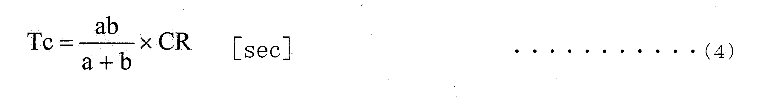
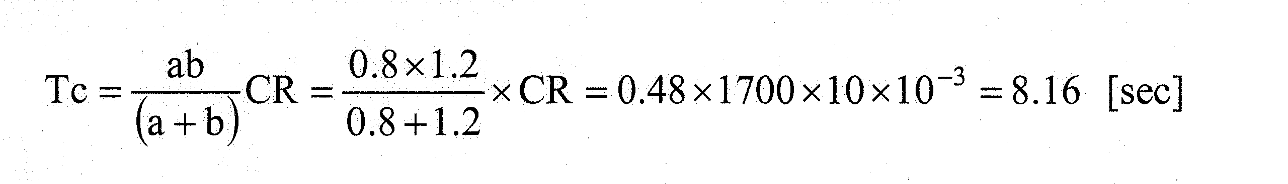
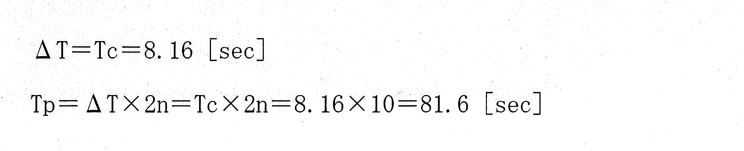
- [Sec] (Constant) Start from parallel connection of capacitors C1 and C2, and the time required to sequentially connect C2 and C3, C3 and C4, ..., C2n-1 and C2n, and C2n and C1 in parallel Tp [ sec]
- Tp [sec] is defined as “one cycle time”.
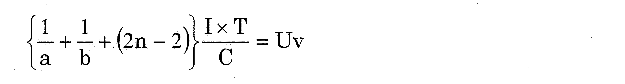
- C [F] be the nominal capacitance of the two capacitors C1 and C2, respectively, let aC [F] be the actual capacitance of the capacitor C1, and bC [F] be the actual capacitance of C2.
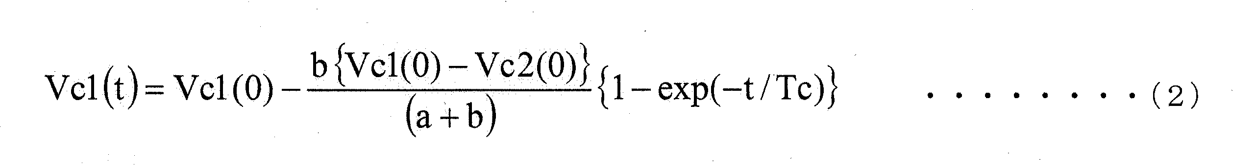
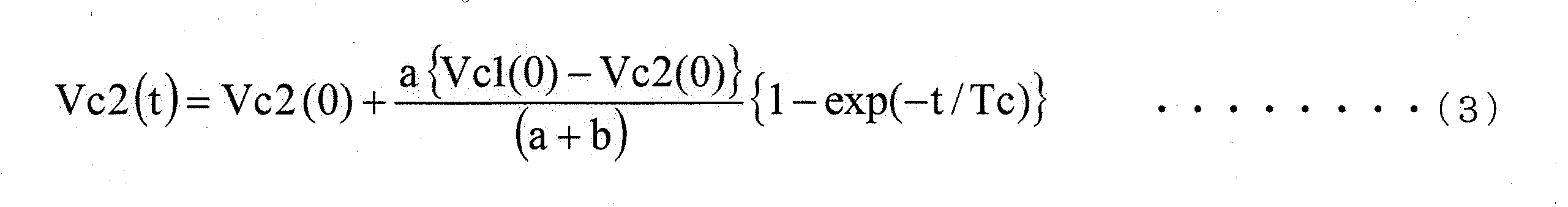
- Vc1 (0) [V] the voltage between the terminals of the capacitor C1 immediately before closing the switch S (time 0)
- Vc2 (0) [V] the voltage between the terminals of the capacitor C2
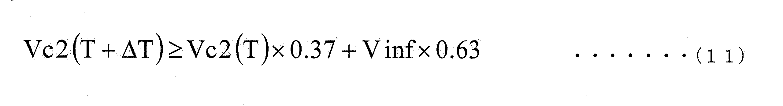
- Fig. 8 shows the change over time in the voltage across the capacitors C1 and C2.
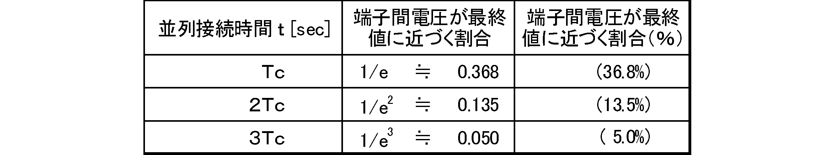
- equalization is started at the time constant Tc expressed by the equation (4), and the voltage between the terminals of the two capacitors is the same in a steady state after a sufficient time has elapsed.
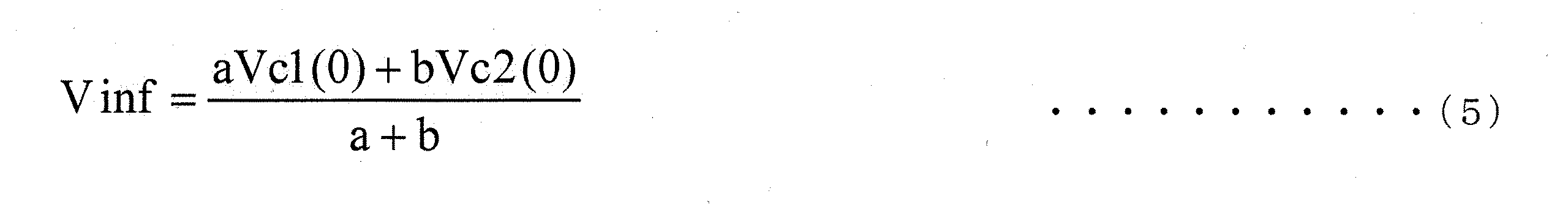
- Vinf the final voltage value in the steady state.
- Vinf This final value Vinf is given by the following equation (5).
- Vc1 (0) ⁇ Vc2 (0) When Vc1 (0) ⁇ Vc2 (0), the direction of current is opposite to that in FIG. 7B, and the magnitude relationship between Vc1 (0) and Vc2 (0) is opposite in FIG. Thus, equalization is performed in the same manner as described above, and therefore only the case of Vc1 (0)> Vc2 (0) will be described below.
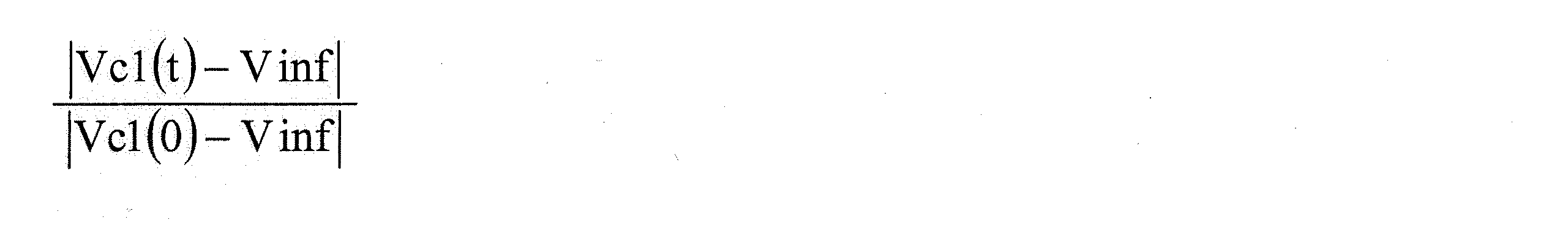
- the ratio at which the voltage between the terminals approaches the final value is that the voltage between the terminals of the capacitor C1 at time t when the switch S in FIG. 7A is closed at time 0 is Vc1 (t).
- FIG. 9 shows temporal changes in the voltage between the terminals of the capacitors C1 and C2 as in FIG.
- the absolute value of the difference between the terminal voltage Vc2 ( ⁇ T) and Vinf of the capacitor C2 at time ⁇ T is also within about 37% of the absolute value of the difference between Vc2 (0) and Vinf.
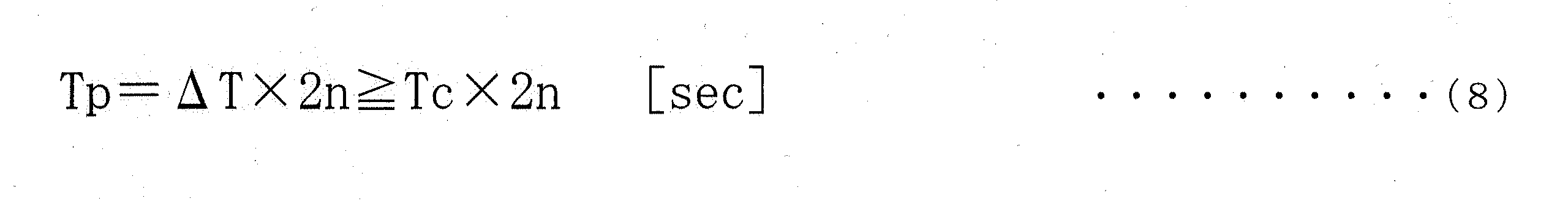
- the power storage unit 21 is composed of 2n capacitors as shown in FIG. 2, starting from the parallel connection of the capacitors C1 and C2, C2 and C3,..., C2n-1 and C2n, and C2n and C1 sequentially.
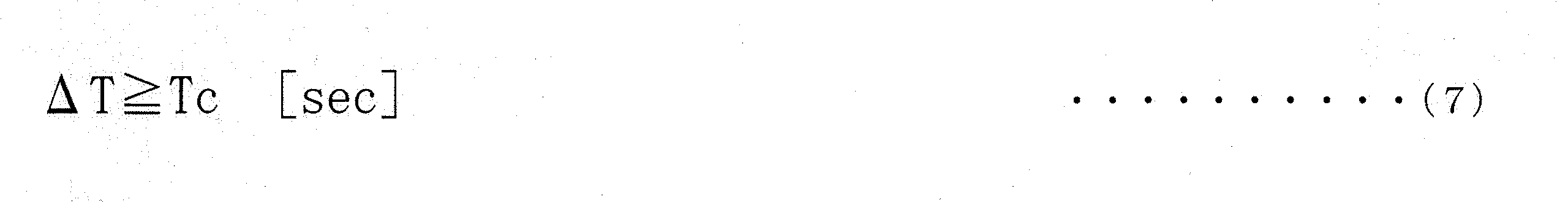
- the one cycle time Tp [sec] required for parallel connection is given by the following equation (8) when ⁇ T is set to a value satisfying the equation (7), for example.
- the power storage unit 21 includes capacitors having the same nominal capacitance and in the same capacitance error range. Therefore, in the following description, the nominal capacitance of the 2n capacitors constituting the power storage unit 21 is C [F], the lower limit value of the capacitance allowed by the rating is aC [F], and the capacitance is allowed by the rating. BC [F] (that is, a ⁇ 1 ⁇ b), and as shown in FIG. 10, the power storage unit 21 sets the capacitance of the capacitor C1 to aC [F] and sets the capacitance of the capacitor C2 to static. It is assumed that the capacitance is bC [F], and the remaining 2n ⁇ 2 capacitors are composed of 2n capacitors where the capacitance is C [F].
- charging is started with the charging current I [A] from the state where all of the 2n capacitors Ci constituting the power storage unit 21 are in a completely discharged state and all the capacitors are connected in series as shown in FIG. Furthermore, the time from the start of charging to the time when charging progresses, the power storage unit voltage Vt reaches the first voltage value Uv [V] set in advance, and immediately before the first series-parallel switching is performed is T [sec]. To do.
- the first voltage value Uv is normally set to the upper limit value of the allowable input voltage range of the power converter 3, but the value at which the conversion efficiency of the power converter 3 is the best, that is, the upper limit of the allowable input voltage range. Even if it is set to a value lower than the value, the effect of the charge control method of the present invention is exhibited.
- the terminal voltage Vc1 (T) at time T of the capacitor C1 having the smallest capacitance and the high terminal voltage is
- the inter-terminal voltage Vc2 (T) of the capacitor C2 having the largest capacitance and the low inter-terminal voltage is
- capacitors C1 and C2 are paralleled and equalized at time T for time ⁇ T.
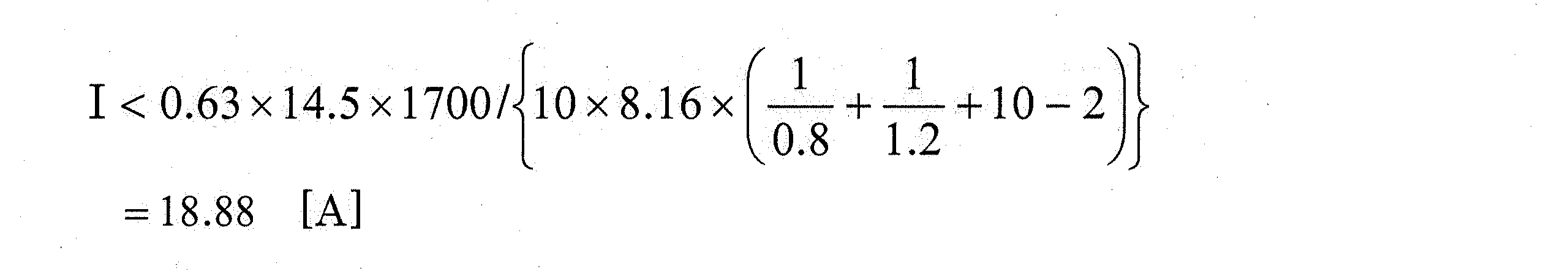
- the charging current during the period ⁇ T in which the capacitor C1 and the capacitor C2 are paralleled is approximately 1 ⁇ 2 that in the series connection state.
- the above equation (12) and In the equation (13), the charging current to each capacitor is calculated as being the same as in the case of series connection.
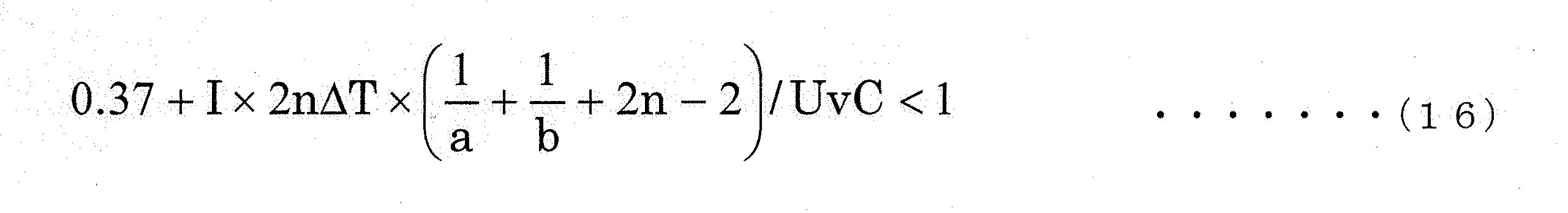
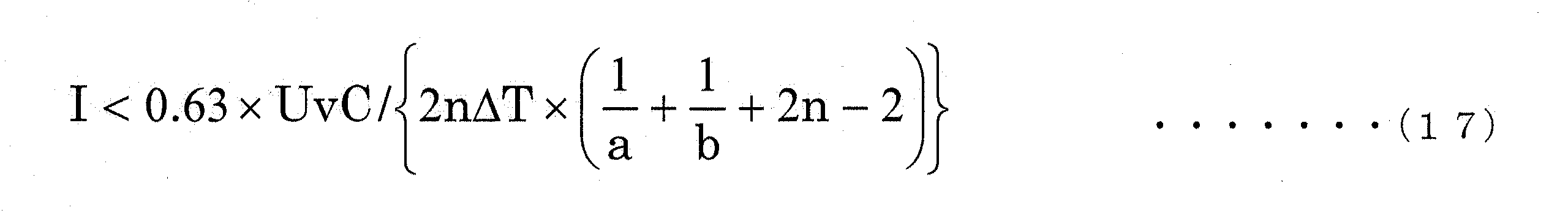
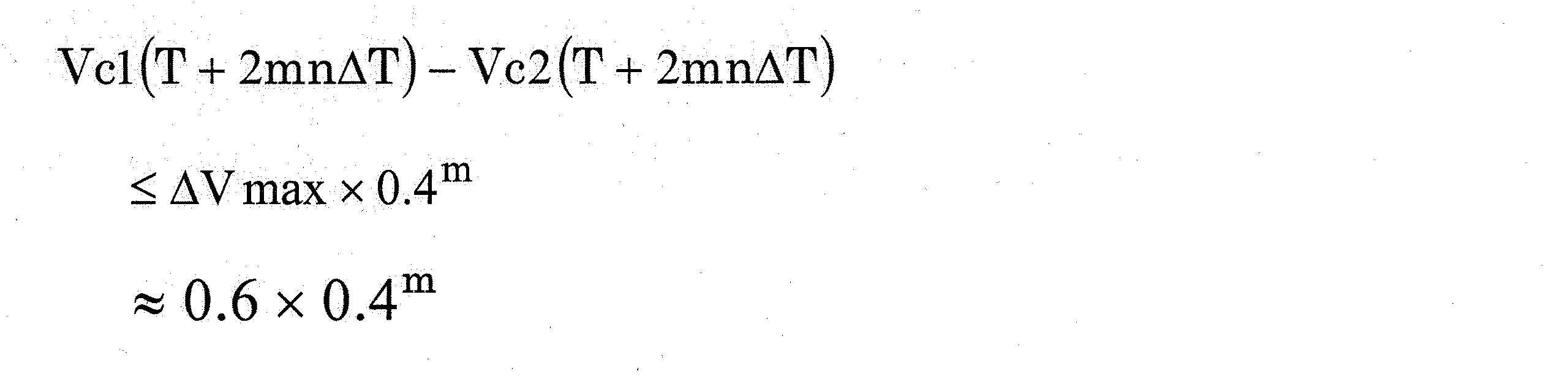
- Vc1 (T + 2n ⁇ T) and Vc2 (T + 2n ⁇ T) are smaller than the values of Equations (12) and (13), and a ⁇ b. Therefore, the values are obtained from Equations (12) and (13).
- the difference between Vc1 (T + 2n ⁇ T) and Vc2 (T + 2n ⁇ T) is expressed larger than the actual value.
- ⁇ T Tc.
- the upper limit value of the charging current expressed by the equation (17) decreases, and m cycles from time T expressed by the equation (18).
- the rate of decrease in the voltage difference between the terminals of the capacitor C1 and the capacitor C2 at the time (T + 2mn ⁇ T) after the time is also reduced.
- the voltage difference between the terminals of the capacitors C1 and C2 is suppressed to about 37% or less of the absolute value of the voltage difference between the terminals just before the parallelization by one parallelization.
- the maximum value of the voltage difference between the terminals of the capacitor C1 and the capacitor C2 after the fourth parallel is about 0.015 [V].
- the value of the transverse current must also be considered.
- a lateral current i flows through the switch S. If this value is excessive, the switch S may be destroyed. is there.
- the switch S is made of a semiconductor, attention must be paid to the value of the transverse current.
- parallelized patterns There are a maximum of 2n combinations of series-parallel capacitors (hereinafter referred to as “parallelized patterns”).
- the number P of parallel parts is n, there are two parallel patterns.
- Pb 1, 2,...
- i 9
- i 9
- the voltage equalizing operation by parallelizing adjacent capacitors is as follows.
- FIG. 17 shows a flowchart of charge control when the power storage unit 21 having the configuration shown in FIG. 2 is used.
- the control circuit 26 sets the switch Si and the switch So shown in FIG. 2 to OFF (open state).
- step S12 the control circuit 26 instructs the series-parallel switching circuit 23 to set the number P of parallel parts to 0 (zero) and connect all the capacitors Ci in series. Thereafter, in step S13, the control circuit 26 closes the switch Si and starts charging.
- step S ⁇ b> 14 the control circuit 26 acquires the storage unit voltage Vt that is the output voltage of the storage unit 21 measured by the storage unit voltage detection circuit 25, and the storage unit voltage detection circuit 24 measures the storage unit voltage 21.
- the terminal voltage Vci of each capacitor Ci is acquired.
- step S15 the control circuit 26 determines whether or not the terminal voltage Vci of each capacitor Ci is equal to or higher than the upper limit value Vcu of the rated voltage. If the inter-terminal voltage Vci of any capacitor Ci is equal to or higher than the upper limit value Vcu of the rated voltage (YES), the process proceeds to step S16 and charging is stopped. That is, the control circuit 26 turns off the switch Si (open state). On the other hand, if the inter-terminal voltage Vci of any capacitor Ci does not exceed the upper limit value Vcu of the rated voltage (NO), the process proceeds to step S17.
- step S17 the control circuit 26 determines whether or not the number P of parallel units is n. When the number P of parallel parts is n (YES), it progresses to the process of step S20 and charging is continued. On the other hand, if the number P of parallel parts is not n (NO), the process proceeds to step S18.
- step S18 the control circuit 26 determines whether or not the power storage unit voltage Vt is equal to or higher than the first voltage value Uv.
- the process proceeds to step S19, and the control circuit 26 instructs the series / parallel switching circuit 23 to increase the number P of parallel units by one.
- the process proceeds to step S20 and the charging is continued. After the processes in steps S19 and S20, the process proceeds to step S21.
- step S21 the control circuit 26 determines whether or not the number P of parallel parts is zero.
- the number P of parallel parts is 0 (YES)
- it progresses to the process of step S23, waits for progress of a time interval, ie, parallel connection time (DELTA) T, and returns to the process of step S14 after that.
- a time interval ie, parallel connection time (DELTA) T
- DELTA parallel connection time
- step S22 the control circuit 26 starts or continues the pressure equalization by parallelizing adjacent capacitors, and then waits for the elapse of the time interval, that is, the parallel connection time ⁇ T in step S23.
- step S18 When charging proceeds from a state in which all the capacitors Ci are connected in series and the power storage unit voltage Vt reaches the preset first voltage value Uv (YES in step S18), a series-parallel switch is performed, and the parallel unit Is set to 1 (step S19). At the same time, pressure equalization is started by parallelizing adjacent capacitors (steps S21 and S22).
- Charging proceeds when the number P of parallel parts is n, and when the voltage Vci between terminals of any one of the capacitors Ci reaches the upper limit value Vcu of the rated voltage, the charging is stopped (steps S14, S15, S16).
- the discharge control method according to the present invention is a state in which the number P of parallel parts is n when a parallel part is formed by connecting two adjacent capacitors in parallel in a power storage part composed of 2n capacitors. From the above, the following first process and second process are repeated until all capacitors are connected in series.
- Pressure equalization by paralleling adjacent capacitors is also performed during the discharge process.
- capacitors having a capacitance error are connected in series, the voltage between terminals of a capacitor having a small capacitance decreases faster than the voltage between terminals of a capacitor having a large capacitance. Therefore, in the discharging process, if voltage equalization is not performed by parallelizing adjacent capacitors, the time until the inter-terminal voltage Vt of the power storage unit 21 reaches the lower limit value of the allowable input voltage range of the power converter 3 is increased. As a result, the discharge time (power converter operating time) is shortened.
- the discharge time of the power storage unit 21 (the operating time of the power converter 3) can be extended by performing equalization by parallelizing adjacent capacitors in the discharge process.
- the number of capacitors constituting the power storage unit 21 is eight as shown in FIG. 4 described above, the number P of parallel units decreases to 4, 3, 2, 1, and finally all capacitors Connected in series.
- an upper limit value and a lower limit value (lower rated voltage) of the rated voltage of the terminal voltage are set.
- the upper limit value and lower limit value of the rated voltage of such a terminal voltage are set for the capacitor constituting the power storage unit 21 and the capacitor is used, overcharging will occur if charging is continued beyond the upper limit value of the rated voltage.
- the electrolyte solution undergoes electrolysis and becomes less than the lower limit value of the rated voltage due to overdischarge, the electrode collapses, causing deterioration, and in the worst case, destruction.
- the power storage unit 21 is configured by 2n capacitors Ci in which only the upper limit value of the rated voltage of the terminal voltage is set will be described.
- the preset second voltage value is Lv.
- the second voltage value Lv is normally set to the lower limit value of the allowable input voltage range of the power converter 3, but the value at which the conversion efficiency of the power converter 3 is the best, that is, the lower limit value of the allowable input voltage range. Even if set to a high value, the effect of the charge control method of the present invention is exhibited.
- FIG. 18 shows a flowchart of the discharge control when the power storage unit 21 is composed of 2n capacitors as shown in FIG.
- steps that perform the same processes as those in the flowchart of FIG. 17 are denoted by the same reference numerals.
- the flow of discharge control will be described with reference to FIGS. 1 and 2 and the flowchart of FIG.
- step S41 the control circuit 26 closes the switch So and starts discharging.
- step S42 the control circuit 26 acquires the power storage unit voltage Vt measured by the power storage unit voltage detection circuit 25. Subsequently, in step S43, the acquired power storage unit voltage Vt is equal to or lower than the preset second voltage value Lv. Determine whether or not. If the power storage unit voltage Vt is equal to or lower than the second voltage value Lv (YES), the process proceeds to step S45. If not (NO), the process proceeds to step S44, and the discharge is continued.
- step S45 the control circuit 26 determines whether or not the number P of parallel parts is zero. If the number P of parallel parts is zero (YES), the process proceeds to step S47 and stops discharging. . That is, the control circuit 26 opens the switch So. On the other hand, if the number P of parallel parts is not zero (NO), the process proceeds to step S46, and the number P of parallel parts is reduced by 1 to (P-1). After the processes of steps S44 and S46 are completed, the process proceeds to step S21.
- step S21 the control circuit 26 determines again whether or not the number P of parallel parts is zero. If the number P of parallel parts is 0 (YES), the process proceeds to step S48, and the adjacent capacitor The pressure equalization by parallelization is stopped, the time interval of step S23, that is, the passage of time corresponding to the parallel connection time ⁇ T is waited, and then the process returns to step S42. On the other hand, when the number P of parallel parts is not 0 (NO), the process proceeds to step S22.
- step S22 the control circuit 26 starts or continues the pressure equalization by parallelizing adjacent capacitors, and then returns to the process of step S42 after waiting for the parallel connection time ⁇ T to elapse in the time interval of step S23.
- the processing of the flowchart of FIG. 18 is summarized as follows.
- the series-parallel switching is performed.
- the number P of parallel parts is decreased by 1 (steps S45 and S46).
- pressure equalization is started by parallelizing adjacent capacitors (steps S21 and S22).
- step S43, S45, S46, S21, S22, S23 the pressure equalization operation by paralleling adjacent capacitors is repeated (steps S43, S45, S46, S21, S22, S23), and the power storage unit voltage Vt reaches the preset second voltage value Lv.
- step S43, S45, S46 the pressure equalization operation by paralleling adjacent capacitors is repeated.
- step S21, S48, S23 If the number P of parallel parts becomes 0 (that is, a state in which all capacitors are connected in series), voltage equalization by parallelizing adjacent capacitors is stopped, but discharging continues (steps S21, S48, S23).
- FIG. 19 shows a flowchart when the charge control method and the discharge control method of the present invention are implemented in combination.
- FIG. 19 is a flowchart in the case where the charging power is larger than the discharging power.
- the same steps as those in FIGS. 17 and 18 are denoted by the same reference numerals.
- the flowchart of FIG. 19 will be described focusing on steps different from the flowcharts of FIGS. 17 and 18.
- Step S19 the power storage unit voltage Vt reaches the upper limit value Uv of the allowable input voltage range of the power converter 3
- step S22 the pressure equalization process by parallelizing adjacent capacitors is not performed.
- Discharge is started when power storage unit voltage Vt exceeds lower limit Lv of the allowable input voltage range of power converter 3 (steps S43 and S62).
- FIG. 20 shows a flowchart in the case where the capacitor Ci in which the upper limit value and the lower limit value of the rated voltage are set is used for the power storage unit and the charge control method and the discharge control method are combined, that is, when discharging is performed while charging.
- the upper limit value of the rated voltage of the terminal voltage of each capacitor is indicated as Vcu
- the lower limit value of the rated voltage is indicated as Vcl.
- step S71 the control circuit 26 determines whether or not the terminal voltage Vci of each capacitor Ci is equal to or lower than the lower limit value Vcl of the rated voltage, and the terminal voltage Vci of any one of the capacitors Ci is the lower limit value of the rated voltage. If Vcl or less (YES), the process proceeds to step S72 to turn on charging (ie, close the switch Si) and turn off discharging (ie, open the switch So). On the other hand, when the inter-terminal voltage Vci of all the capacitors Ci is higher than the lower limit value Vcl of the rated voltage (NO), the process proceeds to step S15.
- the capacitor of the power storage unit is composed of 2n capacitors in which the upper limit value and the lower limit value of the rated voltage are set to the inter-terminal voltage, and the charge control method and the discharge control method are combined. Since charge is transferred from a capacitor having a large voltage between terminals to a capacitor having a small voltage between terminals by equalizing pressure by parallelizing adjacent capacitors, if an appropriate parallel connection time ⁇ T is selected, all of the power storage units are configured. The voltage between the terminals of the capacitors is kept almost equal except when all the capacitors are connected in series.
- FIG. 21A shows temporal changes in the voltage Vci between terminals of each capacitor Ci when charge control and discharge control are performed by the method of the present invention.
- the power storage unit 21 is configured using ten capacitors having a nominal capacitance of 1700 [F], and charging control is performed according to the flowchart of FIG. 19 is a graph showing a temporal change in the voltage Vci between terminals of each capacitor Ci when the load 4 is connected via the power converter 3 and discharge control is performed according to the flowchart of FIG.
- FIG. 21B shows the time of the voltage Vci between the terminals of each capacitor Ci when the power storage unit having the same configuration as the method of the present invention is used and the charge control and the discharge control are performed by the method of Patent Document 2. It is the graph which showed the change.
- FIG. 22A shows the inter-terminal voltage Vci of each capacitor Ci when charging is controlled by the method of the present invention and charging is stopped (full charge).
- FIG. The charge control is performed by this method, and the inter-terminal voltage Vci of each capacitor Ci at the time of full charge is shown.
- the charging current was 2 [A]
- the load at the time of discharging was 8 [W]
- the parallel connection time ⁇ T in equalizing pressure by parallelizing adjacent capacitors was 10 [sec]. Therefore, one cycle time Tp is 100 [sec].
- the allowable input voltage range of the power converter (DC-AC inverter) 3 is 10.7 to 15.0 [V], but the conversion efficiency decreases near the upper limit or lower limit of the allowable input voltage range.
- the value Uv was 14.5 [V]
- the second voltage value Lv was 11.5 [V].
- all the capacitors started charge from the state of complete discharge, and after discharging to full charge, it discharged.
- the accurate charging time was 1 hour 6 minutes 36 seconds when the control method of the present invention was used, and 1 hour 6 minutes 35 seconds when the control method of Patent Document 2 was used.
- pressure equalization is performed by parallelizing adjacent capacitors, which takes time. Nevertheless, the charging time was almost the same.
- control method of the present invention has less variation in the inter-terminal voltage than the control method of Patent Document 2. This point is clearer when FIG. 22 (a) and FIG. 22 (b) showing the variation in the voltage between the terminals of each capacitor at the end of charging (full charge) are compared.
- the control method of the present invention has less variation in the voltage between terminals of each capacitor at the end of charging (full charge) than the control method of Patent Document 2.
- the maximum value of the voltage difference between terminals of each capacitor at full charge was 0.017 [V] in the control method of the present invention, whereas 0.047 [V] in the control method of Patent Document 2.
- the effectiveness of pressure equalization by parallelizing adjacent capacitors was confirmed.
- the charging process ends when any one of the capacitors constituting the power storage unit 21 reaches the rated voltage. Therefore, if the variation in the voltage between terminals of each capacitor is large at this time, the amount of unstored power increases.
- the unstored power amount in the case of the control method of the present invention was 313.3 [J]
- the unstored power amount in the case of the control method of Patent Document 2 is 761.9 [J]. From the viewpoint of charging efficiency, it can be seen that the control method of the present invention is effective.
Landscapes
- Engineering & Computer Science (AREA)
- Power Engineering (AREA)
- Charge And Discharge Circuits For Batteries Or The Like (AREA)
- Secondary Cells (AREA)
Abstract
Description
並列に接続された2つの電気二重層キャパシタを並列部としたときに、前記電気二重層キャパシタが全て直列に接続された状態から充電を開始し、前記並列部の数Pがnになり、かつ、2n個の電気二重層キャパシタの少なくともいずれかの1つの端子間電圧が定格電圧の上限値に達するまで、下記第1の処理と第2の処理とを繰り返すことを特徴とする。
(1)前記並列部の数Pが1以上の場合に、iを1から2nまでの値を循環する整数とし、kj(jは1≦j≦Pの整数)を0≦kj≦2n-2を満たすP個の0または任意の偶数とし、所定の時間経過毎に、iの数を1ずつ増やしながら、(i+kj)番目と(i+kj+1)番目の電気二重層キャパシタの接続状態を、前記並列部を構成するように並列にすると共に、他の電気二重層キャパシタの接続状態を直列にする。ここで、Kを整数としたときに(2n+K)番目の電気二重層キャパシタはK番目の電気二重層キャパシタとなる。
(2)前記蓄電手段の電圧が、あらかじめ設定した第1の電圧値に到ったときに、前記並列部の数Pを1つ増やす。
並列に接続された2つの電気二重層キャパシタを並列部としたときに、前記並列部の数Pがnの状態から電気二重層キャパシタが全て直列に接続された状態になり、かつ、前記蓄電手段の電圧が、あらかじめ設定した第2の電圧値に到るまで、下記第1の処理と第2の処理とを繰り返すことを特徴とする。
(1)前記並列部の数Pが1以上の場合に、iを1から2nまでの値を循環する整数とし、kj(jは1≦j≦Pの整数)を0≦kj≦2n-2を満たすP個の0または任意の偶数とし、所定の時間経過毎に、iの数を1ずつ増やしながら、(i+kj)番目と(i+kj+1)番目の電気二重層キャパシタの接続状態を、前記並列部を構成するように並列にすると共に、その他の電気二重層キャパシタの接続状態を直列にする。ここで、Kを整数としたときに(2n+K)番目の電気二重層キャパシタはK番目の電気二重層キャパシタとなる。
(2)前記蓄電手段の電圧が、前記第2の電圧値に到ったときに、前記並列部の数Pを1つ減らす。
図1に、蓄電装置を含む電力供給システムの構成を示す。本実施の形態では、図1の蓄電装置2によって実施される充電制御方法について説明する。蓄電装置2は、直流電源1から供給された直流電力を蓄電し、これを、電力変換器3において交流電力に変換した後、あるいは直流電力のまま負荷4に供給する。
次に、蓄電装置の構成について説明する。蓄電装置2は、蓄電部21および制御部22を備えている。蓄電部21は、直流電源1から供給された直流の電力を蓄積する。制御部22は、蓄電部21における充放電を制御する。
次に、本発明におけるキャパシタCiの接続状態の切り換え制御について説明する。
(1)前記並列部の数Pが1以上の場合に、iを1から2nまでの値を循環する整数とし、kj(jは1≦j≦Pの整数)を0≦kj≦2n-2を満たすP個の0または任意の偶数とし、所定の時間経過毎に、iの数を1ずつ増やしながら、(i+kj)番目と(i+kj+1)番目のキャパシタの接続状態を、前記並列部を構成するように並列にすると共に、その他のキャパシタの接続状態を直列にする。ここで、Kを整数としたときに(2n+K)番目のキャパシタはK番目のキャパシタとなる。
(2)蓄電手段である蓄電部21の電圧が、あらかじめ設定した第1の電圧値に到ったときに、前記並列部の数Pを1つ増やす。


次に、本発明にかかる充電制御方法について、充電制御の流れを説明する。
本実施の形態では、本発明にかかる放電制御方法について説明する。なお、放電制御に用いる蓄電装置2および蓄電部21の構成は、実施の形態1で説明した構成と同じである。
(1)前記並列部の数Pが1以上の場合に、iを1から2nまでの値を循環する整数とし、kj(jは1≦j≦Pの整数)を0≦kj≦2n-2を満たすP個の0または任意の偶数とし、所定の時間経過毎に、iの数を1ずつ増やしながら、(i+kj)番目と(i+kj+1)番目の電気二重層キャパシタの接続状態を、前記並列部を構成するように並列にすると共に、他の電気二重層キャパシタの接続状態を直列にする。ここで、Kを整数としたときに(2n+K)番目の電気二重層キャパシタはK番目の電気二重層キャパシタとなる。
(2)前記蓄電手段の電圧が、あらかじめ設定した第2の電圧値に到ったときに、前記並列部の数Pを1つ減らす。
図18に、蓄電部21が図2のように2n個のキャパシタで構成される場合の放電制御のフローチャートを示す。なお、図中、図17のフローチャートのステップと同一の処理を行うステップについては、同一の符号を付している。以下、図1および図2、ならびに図18のフローチャートを用いて、放電制御の流れを説明する。
本実施の形態では、本発明にかかる充電制御方法と放電制御方法とを組み合わせた場合、すなわち充電しながら放電を行う場合について説明する。図19は、本発明の充電制御方法と放電制御方法を組み合わせて実施する場合のフローチャートを示す。
図21(a)に、本発明の方法により充電制御と放電制御を行った場合の各キャパシタCiの端子間電圧Vciの時間的変化を示す。具体的には、図21(a)は、公称静電容量1700[F]のキャパシタを10個用いて蓄電部21を構成し、図17のフローチャートに従って充電制御を行い、全てのキャパシタが満充電になった後、電力変換器3を介して負荷4を接続し、図18のフローチャートに従って放電制御を行った場合の各キャパシタCiの端子間電圧Vciの時間的変化を示したグラフである。一方、図21(b)は、本発明の方法と同様の構成の蓄電部を用い、特許文献2の方法により充電制御と放電制御を行った場合の、各キャパシタCiの端子間電圧Vciの時間的変化を示したグラフである。

2 蓄電装置
3 電力変換器
4 負荷
21 蓄電部
22 制御部
23 直並列切り換え回路
24 端子間電圧検出回路
25 蓄電部電圧検出回路
26 制御回路
27 パルス生成回路
Ci(i=1、2、…、2n) キャパシタ
S スイッチ
Claims (5)
- 蓄電手段として、静電容量の等しい1番目から2n番目の2n個(nは2以上の整数)の電気二重層キャパシタを含み、かつ隣接する電気二重層キャパシタの間がスイッチにより直列または並列のいずれかに接続でき、また2n番目の電気二重層キャパシタと1番目の電気二重層キャパシタとの間がスイッチにより並列接続できるように構成されたキャパシタ群を用いた蓄電装置の充電制御方法であって、
並列に接続された2つの電気二重層キャパシタを並列部としたときに、前記電気二重層キャパシタが全て直列に接続された状態から充電を開始し、前記並列部の数Pがnになり、かつ、2n個の電気二重層キャパシタの少なくともいずれかの1つの端子間電圧が定格電圧の上限値に達するまで、下記第1の処理と第2の処理とを繰り返すことを特徴とする蓄電装置の充電制御方法。
(1)前記並列部の数Pが1以上の場合に、iを1から2nまでの値を循環する整数とし、kj(jは1≦j≦Pの整数)を0≦kj≦2n-2を満たすP個の0または任意の偶数とし、所定の時間経過毎に、iの数を1ずつ増やしながら、(i+kj)番目と(i+kj+1)番目の電気二重層キャパシタの接続状態を、前記並列部を構成するように並列にすると共に、他の電気二重層キャパシタの接続状態を直列にする。ここで、Kを整数としたときに(2n+K)番目の電気二重層キャパシタはK番目の電気二重層キャパシタとなる。
(2)前記蓄電手段の電圧が、あらかじめ設定した第1の電圧値に到ったときに、前記並列部の数Pを1つ増やす。 - 前記第1の電圧値として、前記蓄電手段の出力側に接続された電力変換器の許容入力電圧範囲の上限値を用いることを特徴とする、請求項1に記載の蓄電装置の充電制御方法。
- 蓄電手段として、静電容量の等しい1番目から2n番目の2n個(nは2以上の整数)の電気二重層キャパシタを含み、かつ隣接する電気二重層キャパシタの間がスイッチにより直列または並列のいずれかに接続でき、また2n番目の電気二重層キャパシタと1番目の電気二重層キャパシタとの間がスイッチにより並列接続できるように構成されたキャパシタ群を用いた蓄電装置の放電制御方法であって、
並列に接続された2つの電気二重層キャパシタを並列部としたときに、前記並列部の数Pがnの状態から電気二重層キャパシタが全て直列に接続された状態になり、かつ、前記蓄電手段の電圧が、あらかじめ設定した第2の電圧値に到るまで、下記第1の処理と第2の処理とを繰り返すことを特徴とする蓄電装置の放電制御方法。
(1)前記並列部の数Pが1以上の場合に、iを1から2nまでの値を循環する整数とし、kj(jは1≦j≦Pの整数)を0≦kj≦2n-2を満たすP個の0または任意の偶数とし、所定の時間経過毎に、iの数を1ずつ増やしながら、(i+kj)番目と(i+kj+1)番目の電気二重層キャパシタの接続状態を、前記並列部を構成するように並列にすると共に、その他の電気二重層キャパシタの接続状態を直列にする。ここで、Kを整数としたときに(2n+K)番目の電気二重層キャパシタはK番目の電気二重層キャパシタとなる。
(2)前記蓄電手段の電圧が、前記第2の電圧値に到ったときに、前記並列部の数Pを1つ減らす。 - 前記第2の電圧値として、前記蓄電手段の出力側に接続された電力変換器の許容入力電圧範囲の下限値を用いることを特徴とする、請求項3に記載の蓄電装置の放電制御方法。
- 前記電気二重層キャパシタとして、定格電圧の下限値が設定されているキャパシタを用いた場合には、前記蓄電手段を構成するいずれかの電気二重層キャパシタの端子間電圧が前記定格電圧の下限値を下回ったときに放電を停止することを特徴とする、請求項3に記載の蓄電装置の放電制御方法。
Priority Applications (8)
| Application Number | Priority Date | Filing Date | Title |
|---|---|---|---|
| SG2013004627A SG187574A1 (en) | 2010-07-27 | 2010-07-27 | Charge control method and discharge control method for electric storage apparatus |
| KR1020137004771A KR101452778B1 (ko) | 2010-07-27 | 2010-07-27 | 축전장치의 충전제어방법 및 방전제어방법 |
| EP10855291.0A EP2600486B1 (en) | 2010-07-27 | 2010-07-27 | Charging control method and discharging control method for electricity storage device |
| JP2011540990A JP4977804B2 (ja) | 2010-07-27 | 2010-07-27 | 蓄電装置の充電制御方法および放電制御方法 |
| PCT/JP2010/062606 WO2012014281A1 (ja) | 2010-07-27 | 2010-07-27 | 蓄電装置の充電制御方法および放電制御方法 |
| MX2013001026A MX2013001026A (es) | 2010-07-27 | 2010-07-27 | Metodo de control de carga y metodo decontrol de descarga para un aparato de almacenamiento de electricidad. |
| CN201080068235.4A CN103190056B (zh) | 2010-07-27 | 2010-07-27 | 蓄电装置的充电控制方法以及放电控制方法 |
| US13/749,993 US9312703B2 (en) | 2010-07-27 | 2013-01-25 | Charge control method and discharge control method for electric storage apparatus |
Applications Claiming Priority (1)
| Application Number | Priority Date | Filing Date | Title |
|---|---|---|---|
| PCT/JP2010/062606 WO2012014281A1 (ja) | 2010-07-27 | 2010-07-27 | 蓄電装置の充電制御方法および放電制御方法 |
Related Child Applications (1)
| Application Number | Title | Priority Date | Filing Date |
|---|---|---|---|
| US13/749,993 Continuation US9312703B2 (en) | 2010-07-27 | 2013-01-25 | Charge control method and discharge control method for electric storage apparatus |
Publications (1)
| Publication Number | Publication Date |
|---|---|
| WO2012014281A1 true WO2012014281A1 (ja) | 2012-02-02 |
Family
ID=45529529
Family Applications (1)
| Application Number | Title | Priority Date | Filing Date |
|---|---|---|---|
| PCT/JP2010/062606 Ceased WO2012014281A1 (ja) | 2010-07-27 | 2010-07-27 | 蓄電装置の充電制御方法および放電制御方法 |
Country Status (8)
| Country | Link |
|---|---|
| US (1) | US9312703B2 (ja) |
| EP (1) | EP2600486B1 (ja) |
| JP (1) | JP4977804B2 (ja) |
| KR (1) | KR101452778B1 (ja) |
| CN (1) | CN103190056B (ja) |
| MX (1) | MX2013001026A (ja) |
| SG (1) | SG187574A1 (ja) |
| WO (1) | WO2012014281A1 (ja) |
Cited By (3)
| Publication number | Priority date | Publication date | Assignee | Title |
|---|---|---|---|---|
| JP2014180091A (ja) * | 2013-03-14 | 2014-09-25 | Npo Hiroshima Junkangata Shakai Suishin Kiko | 二次電池リコンディション装置 |
| JP5828467B1 (ja) * | 2014-10-21 | 2015-12-09 | 太陽パーツ株式会社 | 蓄電装置 |
| KR20160124233A (ko) | 2014-06-10 | 2016-10-26 | 가부시키가이샤 카그라 | 축전 소자의 충전 방법 및 축전 장치 |
Families Citing this family (30)
| Publication number | Priority date | Publication date | Assignee | Title |
|---|---|---|---|---|
| CN102118043B (zh) * | 2009-12-31 | 2013-12-04 | 比亚迪股份有限公司 | 用于对动力电池充电的太阳能充电器 |
| EP2456040A1 (de) * | 2010-11-19 | 2012-05-23 | Flextronic Int.Kft | Schaltung zum Speichern elektrischer Energie |
| WO2012072168A2 (de) | 2010-11-30 | 2012-06-07 | Technische Universität München | Neue multilevelkonvertertopologie mit der möglichkeit zur dynamischen seriell- und parallelschaltung von einzelmodulen |
| DE102011108920B4 (de) * | 2011-07-29 | 2013-04-11 | Technische Universität München | Elektrisches Umrichtersystem |
| JP5874350B2 (ja) * | 2011-11-28 | 2016-03-02 | オムロン株式会社 | 電圧変換回路、および電子機器 |
| US9136713B1 (en) * | 2012-01-13 | 2015-09-15 | Win Cheng | Proactive and highly efficient active balance apparatus for a battery power system |
| JP6223171B2 (ja) * | 2012-12-28 | 2017-11-01 | 株式会社半導体エネルギー研究所 | 蓄電装置の制御システム、蓄電システム、及び電気機器 |
| JP6260106B2 (ja) | 2013-04-25 | 2018-01-17 | 株式会社Gsユアサ | 蓄電装置 |
| US9728985B2 (en) * | 2014-04-11 | 2017-08-08 | Panasonic Corporation | Charging device and charging method for charging a plurality of secondary battery-equipped devices |
| DE102014110410A1 (de) | 2014-07-23 | 2016-01-28 | Universität der Bundeswehr München | Modulares Energiespeicher-Direktumrichtersystem |
| WO2016029202A1 (en) * | 2014-08-22 | 2016-02-25 | Pathion Inc. | Method and apparatus for performing string-level dynamic reconfiguration in an energy system |
| WO2016098802A1 (ja) * | 2014-12-18 | 2016-06-23 | 株式会社フジクラ | 蓄電システム、及び蓄電方法 |
| TWI581538B (zh) * | 2015-03-24 | 2017-05-01 | Fu-Zi Xu | Capacitive stacking device with damping function |
| CN106160239B (zh) * | 2015-03-31 | 2018-11-02 | 徐夫子 | 具阻尼功能的储电装置 |
| US9461483B1 (en) * | 2015-05-26 | 2016-10-04 | Fu-Tzu HSU | Electrical energy storage device with damping function |
| JP6419025B2 (ja) * | 2015-05-27 | 2018-11-07 | キヤノン株式会社 | 電力供給装置、プリンタ及び制御方法 |
| WO2018043222A1 (ja) * | 2016-08-30 | 2018-03-08 | パナソニックIpマネジメント株式会社 | 管理装置、及び蓄電システム |
| CN107800289A (zh) * | 2016-08-31 | 2018-03-13 | 无锡昊阳新能源科技有限公司 | 光伏直流电压电容降压装置 |
| US10270368B2 (en) * | 2016-12-02 | 2019-04-23 | Lawrence Livermore National Security, Llc | Bi-directional, transformerless voltage system |
| CN106786998A (zh) * | 2017-02-24 | 2017-05-31 | 维沃移动通信有限公司 | 一种充放电电路、移动终端及电池充放电的控制方法 |
| DE102017108084B4 (de) * | 2017-04-13 | 2023-08-31 | Universität der Bundeswehr München | Pulsquelle und Verfahren für die magnetisch induktive Nervenreizung |
| CN108735248B (zh) * | 2017-04-24 | 2020-12-25 | 北京兆易创新科技股份有限公司 | 一种电压pump的控制方法和控制装置 |
| CN110611423B (zh) * | 2019-03-26 | 2021-01-19 | 西安交通大学 | 一种转置混联电容阵列结构的设计方法 |
| US10924006B1 (en) * | 2019-09-30 | 2021-02-16 | Psemi Corporation | Suppression of rebalancing currents in a switched-capacitor network |
| US11431243B2 (en) * | 2020-02-28 | 2022-08-30 | Smart Prong Technologies, Inc. | Pre-charging a voltage converter |
| CN112202420B (zh) * | 2020-10-14 | 2022-02-15 | 电子科技大学成都学院 | 一种可编程电容基本电路单元以及基于该电路单元并联和串联的电容选调电路 |
| US12556009B2 (en) * | 2021-01-19 | 2026-02-17 | The Boeing Company | Reconfigurable battery system for efficient charging and discharging |
| KR102622789B1 (ko) * | 2021-03-17 | 2024-01-10 | 금오공과대학교 산학협력단 | 모듈식 배터리 관리 시스템 |
| JP7301100B2 (ja) * | 2021-08-10 | 2023-06-30 | 本田技研工業株式会社 | 交流発生回路、および交流発生装置 |
| JPWO2024134937A1 (ja) * | 2022-12-22 | 2024-06-27 |
Citations (4)
| Publication number | Priority date | Publication date | Assignee | Title |
|---|---|---|---|---|
| JPH11215695A (ja) | 1998-01-28 | 1999-08-06 | Okamura Kenkyusho:Kk | 直並列切換型電源装置 |
| JP2002010501A (ja) * | 2000-06-23 | 2002-01-11 | Honda Motor Co Ltd | 蓄電装置の容量均等化装置 |
| WO2007046138A1 (ja) | 2005-10-19 | 2007-04-26 | Limited Company Tm | キャパシタを用いた蓄電装置とその制御方法 |
| JP2008079364A (ja) * | 2006-09-19 | 2008-04-03 | Toshiba Corp | 充放電装置 |
Family Cites Families (4)
| Publication number | Priority date | Publication date | Assignee | Title |
|---|---|---|---|---|
| US6642692B2 (en) * | 2000-06-23 | 2003-11-04 | Honda Giken Kogyo Kabushiki Kaisha | Charge equalizing device for power storage unit |
| JP4940817B2 (ja) * | 2006-08-04 | 2012-05-30 | パナソニック株式会社 | 蓄電装置 |
| JP4352183B2 (ja) * | 2007-02-28 | 2009-10-28 | 独立行政法人 宇宙航空研究開発機構 | 蓄電モジュール |
| DE202008017360U1 (de) * | 2008-04-18 | 2009-08-06 | Forschungszentrum Karlsruhe Gmbh | Ladestation zum Laden eines Kondensatorenblocks und Verbraucher zum Entladen desselben |
-
2010
- 2010-07-27 KR KR1020137004771A patent/KR101452778B1/ko not_active Expired - Fee Related
- 2010-07-27 EP EP10855291.0A patent/EP2600486B1/en not_active Not-in-force
- 2010-07-27 MX MX2013001026A patent/MX2013001026A/es active IP Right Grant
- 2010-07-27 JP JP2011540990A patent/JP4977804B2/ja active Active
- 2010-07-27 SG SG2013004627A patent/SG187574A1/en unknown
- 2010-07-27 CN CN201080068235.4A patent/CN103190056B/zh not_active Expired - Fee Related
- 2010-07-27 WO PCT/JP2010/062606 patent/WO2012014281A1/ja not_active Ceased
-
2013
- 2013-01-25 US US13/749,993 patent/US9312703B2/en not_active Expired - Fee Related
Patent Citations (4)
| Publication number | Priority date | Publication date | Assignee | Title |
|---|---|---|---|---|
| JPH11215695A (ja) | 1998-01-28 | 1999-08-06 | Okamura Kenkyusho:Kk | 直並列切換型電源装置 |
| JP2002010501A (ja) * | 2000-06-23 | 2002-01-11 | Honda Motor Co Ltd | 蓄電装置の容量均等化装置 |
| WO2007046138A1 (ja) | 2005-10-19 | 2007-04-26 | Limited Company Tm | キャパシタを用いた蓄電装置とその制御方法 |
| JP2008079364A (ja) * | 2006-09-19 | 2008-04-03 | Toshiba Corp | 充放電装置 |
Non-Patent Citations (1)
| Title |
|---|
| See also references of EP2600486A4 |
Cited By (4)
| Publication number | Priority date | Publication date | Assignee | Title |
|---|---|---|---|---|
| JP2014180091A (ja) * | 2013-03-14 | 2014-09-25 | Npo Hiroshima Junkangata Shakai Suishin Kiko | 二次電池リコンディション装置 |
| KR20160124233A (ko) | 2014-06-10 | 2016-10-26 | 가부시키가이샤 카그라 | 축전 소자의 충전 방법 및 축전 장치 |
| US10833523B2 (en) | 2014-06-10 | 2020-11-10 | Kagra Inc. | Electricity storage element charging method and electricity storage device |
| JP5828467B1 (ja) * | 2014-10-21 | 2015-12-09 | 太陽パーツ株式会社 | 蓄電装置 |
Also Published As
| Publication number | Publication date |
|---|---|
| EP2600486A1 (en) | 2013-06-05 |
| US9312703B2 (en) | 2016-04-12 |
| SG187574A1 (en) | 2013-03-28 |
| KR101452778B1 (ko) | 2014-10-22 |
| CN103190056A (zh) | 2013-07-03 |
| MX2013001026A (es) | 2013-10-28 |
| KR20130084289A (ko) | 2013-07-24 |
| EP2600486B1 (en) | 2016-08-17 |
| EP2600486A4 (en) | 2015-09-16 |
| US20130200860A1 (en) | 2013-08-08 |
| JPWO2012014281A1 (ja) | 2013-09-09 |
| JP4977804B2 (ja) | 2012-07-18 |
| CN103190056B (zh) | 2015-07-08 |
Similar Documents
| Publication | Publication Date | Title |
|---|---|---|
| JP4977804B2 (ja) | 蓄電装置の充電制御方法および放電制御方法 | |
| JP4368924B2 (ja) | キャパシタを用いた蓄電装置とその制御方法 | |
| US9941735B2 (en) | Circuit and method for providing an uninterruptible power supply | |
| CN110281810A (zh) | 智能电池的直流充电 | |
| RU2546978C2 (ru) | Аккумуляторная батарея и система управления аккумуляторной батареей | |
| JP2012019685A (ja) | 複数のバッテリセルを有するバッテリシステムの動作方法及び回路 | |
| CN112655131A (zh) | 蓄电装置和充电方法 | |
| JP2009247145A (ja) | 電源システム | |
| US9257859B2 (en) | Dynamic battery control based on demand | |
| JP2014176226A (ja) | Dc/dc変換装置及び分散電源システム | |
| Hou et al. | A battery power bank of serial battery power modules with buck-boost converters | |
| CN107223304A (zh) | 具有能量存储器的多电平变换器 | |
| CN107342603B (zh) | 用于使用可再生能量的发电系统的电池控制电路 | |
| WO2011132302A1 (ja) | 蓄電装置の充電制御方法および放電制御方法 | |
| JP3594288B2 (ja) | 直列接続段数切り換え式キャパシタ電源装置 | |
| WO2013031934A1 (ja) | 電力連系システム | |
| JP7805554B2 (ja) | 電力変換装置 | |
| JP5755967B2 (ja) | 無停電電源装置 | |
| Chauhan et al. | ZCS Switched-Capacitor Cell Balancing Circuit with Bidirectional Buck-Boost Charging | |
| JP2024041010A (ja) | 電池容量制御装置および蓄電システム | |
| JP2005210774A (ja) | 蓄電装置を含む電力供給システム、及びその蓄電装置における蓄電方法 | |
| RU153793U1 (ru) | Система управления аккумуляторной батареей | |
| JP5554208B2 (ja) | 無停電電源装置 | |
| JP2004336918A (ja) | コンデンサへの充電装置 | |
| JP2015228725A (ja) | 電力変換装置、パワーコンディショナ |
Legal Events
| Date | Code | Title | Description |
|---|---|---|---|
| WWE | Wipo information: entry into national phase |
Ref document number: 2011540990 Country of ref document: JP |
|
| 121 | Ep: the epo has been informed by wipo that ep was designated in this application |
Ref document number: 10855291 Country of ref document: EP Kind code of ref document: A1 |
|
| WWE | Wipo information: entry into national phase |
Ref document number: MX/A/2013/001026 Country of ref document: MX |
|
| NENP | Non-entry into the national phase |
Ref country code: DE |
|
| REEP | Request for entry into the european phase |
Ref document number: 2010855291 Country of ref document: EP |
|
| WWE | Wipo information: entry into national phase |
Ref document number: 2010855291 Country of ref document: EP |
|
| ENP | Entry into the national phase |
Ref document number: 20137004771 Country of ref document: KR Kind code of ref document: A |