WO2012014843A1 - パワー半導体ユニット、パワーモジュール、パワー半導体ユニットの製造方法およびパワーモジュールの製造方法 - Google Patents
パワー半導体ユニット、パワーモジュール、パワー半導体ユニットの製造方法およびパワーモジュールの製造方法 Download PDFInfo
- Publication number
- WO2012014843A1 WO2012014843A1 PCT/JP2011/066854 JP2011066854W WO2012014843A1 WO 2012014843 A1 WO2012014843 A1 WO 2012014843A1 JP 2011066854 W JP2011066854 W JP 2011066854W WO 2012014843 A1 WO2012014843 A1 WO 2012014843A1
- Authority
- WO
- WIPO (PCT)
- Prior art keywords
- power semiconductor
- electrode lead
- lead frame
- semiconductor unit
- heat radiating
- Prior art date
- Legal status (The legal status is an assumption and is not a legal conclusion. Google has not performed a legal analysis and makes no representation as to the accuracy of the status listed.)
- Ceased
Links
Images


Classifications
-
- B—PERFORMING OPERATIONS; TRANSPORTING
- B60—VEHICLES IN GENERAL
- B60L—PROPULSION OF ELECTRICALLY-PROPELLED VEHICLES; SUPPLYING ELECTRIC POWER FOR AUXILIARY EQUIPMENT OF ELECTRICALLY-PROPELLED VEHICLES; ELECTRODYNAMIC BRAKE SYSTEMS FOR VEHICLES IN GENERAL; MAGNETIC SUSPENSION OR LEVITATION FOR VEHICLES; MONITORING OPERATING VARIABLES OF ELECTRICALLY-PROPELLED VEHICLES; ELECTRIC SAFETY DEVICES FOR ELECTRICALLY-PROPELLED VEHICLES
- B60L1/00—Supplying electric power to auxiliary equipment of vehicles
- B60L1/003—Supplying electric power to auxiliary equipment of vehicles to auxiliary motors, e.g. for pumps, compressors
-
- H—ELECTRICITY
- H10—SEMICONDUCTOR DEVICES; ELECTRIC SOLID-STATE DEVICES NOT OTHERWISE PROVIDED FOR
- H10W—GENERIC PACKAGES, INTERCONNECTIONS, CONNECTORS OR OTHER CONSTRUCTIONAL DETAILS OF DEVICES COVERED BY CLASS H10
- H10W70/00—Package substrates; Interposers; Redistribution layers [RDL]
- H10W70/40—Leadframes
- H10W70/461—Leadframes specially adapted for cooling
-
- B—PERFORMING OPERATIONS; TRANSPORTING
- B60—VEHICLES IN GENERAL
- B60L—PROPULSION OF ELECTRICALLY-PROPELLED VEHICLES; SUPPLYING ELECTRIC POWER FOR AUXILIARY EQUIPMENT OF ELECTRICALLY-PROPELLED VEHICLES; ELECTRODYNAMIC BRAKE SYSTEMS FOR VEHICLES IN GENERAL; MAGNETIC SUSPENSION OR LEVITATION FOR VEHICLES; MONITORING OPERATING VARIABLES OF ELECTRICALLY-PROPELLED VEHICLES; ELECTRIC SAFETY DEVICES FOR ELECTRICALLY-PROPELLED VEHICLES
- B60L15/00—Methods, circuits, or devices for controlling the traction-motor speed of electrically-propelled vehicles
- B60L15/007—Physical arrangements or structures of drive train converters specially adapted for the propulsion motors of electric vehicles
-
- B—PERFORMING OPERATIONS; TRANSPORTING
- B60—VEHICLES IN GENERAL
- B60L—PROPULSION OF ELECTRICALLY-PROPELLED VEHICLES; SUPPLYING ELECTRIC POWER FOR AUXILIARY EQUIPMENT OF ELECTRICALLY-PROPELLED VEHICLES; ELECTRODYNAMIC BRAKE SYSTEMS FOR VEHICLES IN GENERAL; MAGNETIC SUSPENSION OR LEVITATION FOR VEHICLES; MONITORING OPERATING VARIABLES OF ELECTRICALLY-PROPELLED VEHICLES; ELECTRIC SAFETY DEVICES FOR ELECTRICALLY-PROPELLED VEHICLES
- B60L3/00—Electric devices on electrically-propelled vehicles for safety purposes; Monitoring operating variables, e.g. speed, deceleration or energy consumption
- B60L3/0023—Detecting, eliminating, remedying or compensating for drive train abnormalities, e.g. failures within the drive train
- B60L3/003—Detecting, eliminating, remedying or compensating for drive train abnormalities, e.g. failures within the drive train relating to inverters
-
- B—PERFORMING OPERATIONS; TRANSPORTING
- B60—VEHICLES IN GENERAL
- B60L—PROPULSION OF ELECTRICALLY-PROPELLED VEHICLES; SUPPLYING ELECTRIC POWER FOR AUXILIARY EQUIPMENT OF ELECTRICALLY-PROPELLED VEHICLES; ELECTRODYNAMIC BRAKE SYSTEMS FOR VEHICLES IN GENERAL; MAGNETIC SUSPENSION OR LEVITATION FOR VEHICLES; MONITORING OPERATING VARIABLES OF ELECTRICALLY-PROPELLED VEHICLES; ELECTRIC SAFETY DEVICES FOR ELECTRICALLY-PROPELLED VEHICLES
- B60L50/00—Electric propulsion with power supplied within the vehicle
- B60L50/10—Electric propulsion with power supplied within the vehicle using propulsion power supplied by engine-driven generators, e.g. generators driven by combustion engines
- B60L50/16—Electric propulsion with power supplied within the vehicle using propulsion power supplied by engine-driven generators, e.g. generators driven by combustion engines with provision for separate direct mechanical propulsion
-
- B—PERFORMING OPERATIONS; TRANSPORTING
- B60—VEHICLES IN GENERAL
- B60L—PROPULSION OF ELECTRICALLY-PROPELLED VEHICLES; SUPPLYING ELECTRIC POWER FOR AUXILIARY EQUIPMENT OF ELECTRICALLY-PROPELLED VEHICLES; ELECTRODYNAMIC BRAKE SYSTEMS FOR VEHICLES IN GENERAL; MAGNETIC SUSPENSION OR LEVITATION FOR VEHICLES; MONITORING OPERATING VARIABLES OF ELECTRICALLY-PROPELLED VEHICLES; ELECTRIC SAFETY DEVICES FOR ELECTRICALLY-PROPELLED VEHICLES
- B60L50/00—Electric propulsion with power supplied within the vehicle
- B60L50/50—Electric propulsion with power supplied within the vehicle using propulsion power supplied by batteries or fuel cells
- B60L50/60—Electric propulsion with power supplied within the vehicle using propulsion power supplied by batteries or fuel cells using power supplied by batteries
- B60L50/61—Electric propulsion with power supplied within the vehicle using propulsion power supplied by batteries or fuel cells using power supplied by batteries by batteries charged by engine-driven generators, e.g. series hybrid electric vehicles
-
- B—PERFORMING OPERATIONS; TRANSPORTING
- B60—VEHICLES IN GENERAL
- B60L—PROPULSION OF ELECTRICALLY-PROPELLED VEHICLES; SUPPLYING ELECTRIC POWER FOR AUXILIARY EQUIPMENT OF ELECTRICALLY-PROPELLED VEHICLES; ELECTRODYNAMIC BRAKE SYSTEMS FOR VEHICLES IN GENERAL; MAGNETIC SUSPENSION OR LEVITATION FOR VEHICLES; MONITORING OPERATING VARIABLES OF ELECTRICALLY-PROPELLED VEHICLES; ELECTRIC SAFETY DEVICES FOR ELECTRICALLY-PROPELLED VEHICLES
- B60L7/00—Electrodynamic brake systems for vehicles in general
- B60L7/10—Dynamic electric regenerative braking
- B60L7/14—Dynamic electric regenerative braking for vehicles propelled by AC motors
-
- H—ELECTRICITY
- H02—GENERATION; CONVERSION OR DISTRIBUTION OF ELECTRIC POWER
- H02M—APPARATUS FOR CONVERSION BETWEEN AC AND AC, BETWEEN AC AND DC, OR BETWEEN DC AND DC, AND FOR USE WITH MAINS OR SIMILAR POWER SUPPLY SYSTEMS; CONVERSION OF DC OR AC INPUT POWER INTO SURGE OUTPUT POWER; CONTROL OR REGULATION THEREOF
- H02M7/00—Conversion of AC power input into DC power output; Conversion of DC power input into AC power output
- H02M7/003—Constructional details, e.g. physical layout, assembly, wiring or busbar connections
-
- H—ELECTRICITY
- H05—ELECTRIC TECHNIQUES NOT OTHERWISE PROVIDED FOR
- H05K—PRINTED CIRCUITS; CASINGS OR CONSTRUCTIONAL DETAILS OF ELECTRIC APPARATUS; MANUFACTURE OF ASSEMBLAGES OF ELECTRICAL COMPONENTS
- H05K7/00—Constructional details common to different types of electric apparatus
- H05K7/20—Modifications to facilitate cooling, ventilating, or heating
- H05K7/2089—Modifications to facilitate cooling, ventilating, or heating for power electronics, e.g. for inverters for controlling motor
- H05K7/20927—Liquid coolant without phase change
-
- H—ELECTRICITY
- H10—SEMICONDUCTOR DEVICES; ELECTRIC SOLID-STATE DEVICES NOT OTHERWISE PROVIDED FOR
- H10W—GENERIC PACKAGES, INTERCONNECTIONS, CONNECTORS OR OTHER CONSTRUCTIONAL DETAILS OF DEVICES COVERED BY CLASS H10
- H10W40/00—Arrangements for thermal protection or thermal control
- H10W40/40—Arrangements for thermal protection or thermal control involving heat exchange by flowing fluids
- H10W40/47—Arrangements for thermal protection or thermal control involving heat exchange by flowing fluids by flowing liquids, e.g. forced water cooling
-
- H—ELECTRICITY
- H10—SEMICONDUCTOR DEVICES; ELECTRIC SOLID-STATE DEVICES NOT OTHERWISE PROVIDED FOR
- H10W—GENERIC PACKAGES, INTERCONNECTIONS, CONNECTORS OR OTHER CONSTRUCTIONAL DETAILS OF DEVICES COVERED BY CLASS H10
- H10W74/00—Encapsulations, e.g. protective coatings
- H10W74/01—Manufacture or treatment
- H10W74/016—Manufacture or treatment using moulds
-
- B—PERFORMING OPERATIONS; TRANSPORTING
- B60—VEHICLES IN GENERAL
- B60L—PROPULSION OF ELECTRICALLY-PROPELLED VEHICLES; SUPPLYING ELECTRIC POWER FOR AUXILIARY EQUIPMENT OF ELECTRICALLY-PROPELLED VEHICLES; ELECTRODYNAMIC BRAKE SYSTEMS FOR VEHICLES IN GENERAL; MAGNETIC SUSPENSION OR LEVITATION FOR VEHICLES; MONITORING OPERATING VARIABLES OF ELECTRICALLY-PROPELLED VEHICLES; ELECTRIC SAFETY DEVICES FOR ELECTRICALLY-PROPELLED VEHICLES
- B60L2210/00—Converter types
- B60L2210/40—DC to AC converters
-
- B—PERFORMING OPERATIONS; TRANSPORTING
- B60—VEHICLES IN GENERAL
- B60L—PROPULSION OF ELECTRICALLY-PROPELLED VEHICLES; SUPPLYING ELECTRIC POWER FOR AUXILIARY EQUIPMENT OF ELECTRICALLY-PROPELLED VEHICLES; ELECTRODYNAMIC BRAKE SYSTEMS FOR VEHICLES IN GENERAL; MAGNETIC SUSPENSION OR LEVITATION FOR VEHICLES; MONITORING OPERATING VARIABLES OF ELECTRICALLY-PROPELLED VEHICLES; ELECTRIC SAFETY DEVICES FOR ELECTRICALLY-PROPELLED VEHICLES
- B60L2220/00—Electrical machine types; Structures or applications thereof
- B60L2220/10—Electrical machine types
- B60L2220/14—Synchronous machines
-
- B—PERFORMING OPERATIONS; TRANSPORTING
- B60—VEHICLES IN GENERAL
- B60L—PROPULSION OF ELECTRICALLY-PROPELLED VEHICLES; SUPPLYING ELECTRIC POWER FOR AUXILIARY EQUIPMENT OF ELECTRICALLY-PROPELLED VEHICLES; ELECTRODYNAMIC BRAKE SYSTEMS FOR VEHICLES IN GENERAL; MAGNETIC SUSPENSION OR LEVITATION FOR VEHICLES; MONITORING OPERATING VARIABLES OF ELECTRICALLY-PROPELLED VEHICLES; ELECTRIC SAFETY DEVICES FOR ELECTRICALLY-PROPELLED VEHICLES
- B60L2240/00—Control parameters of input or output; Target parameters
- B60L2240/10—Vehicle control parameters
- B60L2240/12—Speed
-
- B—PERFORMING OPERATIONS; TRANSPORTING
- B60—VEHICLES IN GENERAL
- B60L—PROPULSION OF ELECTRICALLY-PROPELLED VEHICLES; SUPPLYING ELECTRIC POWER FOR AUXILIARY EQUIPMENT OF ELECTRICALLY-PROPELLED VEHICLES; ELECTRODYNAMIC BRAKE SYSTEMS FOR VEHICLES IN GENERAL; MAGNETIC SUSPENSION OR LEVITATION FOR VEHICLES; MONITORING OPERATING VARIABLES OF ELECTRICALLY-PROPELLED VEHICLES; ELECTRIC SAFETY DEVICES FOR ELECTRICALLY-PROPELLED VEHICLES
- B60L2240/00—Control parameters of input or output; Target parameters
- B60L2240/10—Vehicle control parameters
- B60L2240/36—Temperature of vehicle components or parts
-
- B—PERFORMING OPERATIONS; TRANSPORTING
- B60—VEHICLES IN GENERAL
- B60L—PROPULSION OF ELECTRICALLY-PROPELLED VEHICLES; SUPPLYING ELECTRIC POWER FOR AUXILIARY EQUIPMENT OF ELECTRICALLY-PROPELLED VEHICLES; ELECTRODYNAMIC BRAKE SYSTEMS FOR VEHICLES IN GENERAL; MAGNETIC SUSPENSION OR LEVITATION FOR VEHICLES; MONITORING OPERATING VARIABLES OF ELECTRICALLY-PROPELLED VEHICLES; ELECTRIC SAFETY DEVICES FOR ELECTRICALLY-PROPELLED VEHICLES
- B60L2240/00—Control parameters of input or output; Target parameters
- B60L2240/40—Drive Train control parameters
- B60L2240/52—Drive Train control parameters related to converters
- B60L2240/525—Temperature of converter or components thereof
-
- H—ELECTRICITY
- H10—SEMICONDUCTOR DEVICES; ELECTRIC SOLID-STATE DEVICES NOT OTHERWISE PROVIDED FOR
- H10W—GENERIC PACKAGES, INTERCONNECTIONS, CONNECTORS OR OTHER CONSTRUCTIONAL DETAILS OF DEVICES COVERED BY CLASS H10
- H10W70/00—Package substrates; Interposers; Redistribution layers [RDL]
- H10W70/60—Insulating or insulated package substrates; Interposers; Redistribution layers
- H10W70/67—Insulating or insulated package substrates; Interposers; Redistribution layers characterised by their insulating layers or insulating parts
- H10W70/68—Shapes or dispositions thereof
- H10W70/681—Shapes or dispositions thereof comprising holes not having chips therein, e.g. for outgassing, underfilling or bond wire passage
-
- H—ELECTRICITY
- H10—SEMICONDUCTOR DEVICES; ELECTRIC SOLID-STATE DEVICES NOT OTHERWISE PROVIDED FOR
- H10W—GENERIC PACKAGES, INTERCONNECTIONS, CONNECTORS OR OTHER CONSTRUCTIONAL DETAILS OF DEVICES COVERED BY CLASS H10
- H10W72/00—Interconnections or connectors in packages
- H10W72/071—Connecting or disconnecting
- H10W72/073—Connecting or disconnecting of die-attach connectors
- H10W72/07331—Connecting techniques
- H10W72/07336—Soldering or alloying
-
- H—ELECTRICITY
- H10—SEMICONDUCTOR DEVICES; ELECTRIC SOLID-STATE DEVICES NOT OTHERWISE PROVIDED FOR
- H10W—GENERIC PACKAGES, INTERCONNECTIONS, CONNECTORS OR OTHER CONSTRUCTIONAL DETAILS OF DEVICES COVERED BY CLASS H10
- H10W72/00—Interconnections or connectors in packages
- H10W72/071—Connecting or disconnecting
- H10W72/073—Connecting or disconnecting of die-attach connectors
- H10W72/07331—Connecting techniques
- H10W72/07337—Connecting techniques using a polymer adhesive, e.g. an adhesive based on silicone or epoxy
-
- H—ELECTRICITY
- H10—SEMICONDUCTOR DEVICES; ELECTRIC SOLID-STATE DEVICES NOT OTHERWISE PROVIDED FOR
- H10W—GENERIC PACKAGES, INTERCONNECTIONS, CONNECTORS OR OTHER CONSTRUCTIONAL DETAILS OF DEVICES COVERED BY CLASS H10
- H10W72/00—Interconnections or connectors in packages
- H10W72/071—Connecting or disconnecting
- H10W72/073—Connecting or disconnecting of die-attach connectors
- H10W72/07351—Connecting or disconnecting of die-attach connectors characterised by changes in properties of the die-attach connectors during connecting
-
- H—ELECTRICITY
- H10—SEMICONDUCTOR DEVICES; ELECTRIC SOLID-STATE DEVICES NOT OTHERWISE PROVIDED FOR
- H10W—GENERIC PACKAGES, INTERCONNECTIONS, CONNECTORS OR OTHER CONSTRUCTIONAL DETAILS OF DEVICES COVERED BY CLASS H10
- H10W72/00—Interconnections or connectors in packages
- H10W72/071—Connecting or disconnecting
- H10W72/076—Connecting or disconnecting of strap connectors
- H10W72/07631—Techniques
- H10W72/07636—Soldering or alloying
-
- H—ELECTRICITY
- H10—SEMICONDUCTOR DEVICES; ELECTRIC SOLID-STATE DEVICES NOT OTHERWISE PROVIDED FOR
- H10W—GENERIC PACKAGES, INTERCONNECTIONS, CONNECTORS OR OTHER CONSTRUCTIONAL DETAILS OF DEVICES COVERED BY CLASS H10
- H10W72/00—Interconnections or connectors in packages
- H10W72/071—Connecting or disconnecting
- H10W72/076—Connecting or disconnecting of strap connectors
- H10W72/07631—Techniques
- H10W72/07637—Techniques using a polymer adhesive, e.g. an adhesive based on silicone or epoxy
-
- H—ELECTRICITY
- H10—SEMICONDUCTOR DEVICES; ELECTRIC SOLID-STATE DEVICES NOT OTHERWISE PROVIDED FOR
- H10W—GENERIC PACKAGES, INTERCONNECTIONS, CONNECTORS OR OTHER CONSTRUCTIONAL DETAILS OF DEVICES COVERED BY CLASS H10
- H10W72/00—Interconnections or connectors in packages
- H10W72/071—Connecting or disconnecting
- H10W72/076—Connecting or disconnecting of strap connectors
- H10W72/07651—Connecting or disconnecting of strap connectors characterised by changes in properties of the strap connectors during connecting
- H10W72/07653—Connecting or disconnecting of strap connectors characterised by changes in properties of the strap connectors during connecting changes in shapes
-
- H—ELECTRICITY
- H10—SEMICONDUCTOR DEVICES; ELECTRIC SOLID-STATE DEVICES NOT OTHERWISE PROVIDED FOR
- H10W—GENERIC PACKAGES, INTERCONNECTIONS, CONNECTORS OR OTHER CONSTRUCTIONAL DETAILS OF DEVICES COVERED BY CLASS H10
- H10W72/00—Interconnections or connectors in packages
- H10W72/30—Die-attach connectors
- H10W72/351—Materials of die-attach connectors
- H10W72/352—Materials of die-attach connectors comprising metals or metalloids, e.g. solders
-
- H—ELECTRICITY
- H10—SEMICONDUCTOR DEVICES; ELECTRIC SOLID-STATE DEVICES NOT OTHERWISE PROVIDED FOR
- H10W—GENERIC PACKAGES, INTERCONNECTIONS, CONNECTORS OR OTHER CONSTRUCTIONAL DETAILS OF DEVICES COVERED BY CLASS H10
- H10W72/00—Interconnections or connectors in packages
- H10W72/50—Bond wires
- H10W72/551—Materials of bond wires
- H10W72/552—Materials of bond wires comprising metals or metalloids, e.g. silver
- H10W72/5524—Materials of bond wires comprising metals or metalloids, e.g. silver comprising aluminium [Al]
-
- H—ELECTRICITY
- H10—SEMICONDUCTOR DEVICES; ELECTRIC SOLID-STATE DEVICES NOT OTHERWISE PROVIDED FOR
- H10W—GENERIC PACKAGES, INTERCONNECTIONS, CONNECTORS OR OTHER CONSTRUCTIONAL DETAILS OF DEVICES COVERED BY CLASS H10
- H10W72/00—Interconnections or connectors in packages
- H10W72/60—Strap connectors, e.g. thick copper clips for grounding of power devices
- H10W72/631—Shapes of strap connectors
-
- H—ELECTRICITY
- H10—SEMICONDUCTOR DEVICES; ELECTRIC SOLID-STATE DEVICES NOT OTHERWISE PROVIDED FOR
- H10W—GENERIC PACKAGES, INTERCONNECTIONS, CONNECTORS OR OTHER CONSTRUCTIONAL DETAILS OF DEVICES COVERED BY CLASS H10
- H10W72/00—Interconnections or connectors in packages
- H10W72/851—Dispositions of multiple connectors or interconnections
- H10W72/853—On the same surface
- H10W72/865—Die-attach connectors and bond wires
-
- H—ELECTRICITY
- H10—SEMICONDUCTOR DEVICES; ELECTRIC SOLID-STATE DEVICES NOT OTHERWISE PROVIDED FOR
- H10W—GENERIC PACKAGES, INTERCONNECTIONS, CONNECTORS OR OTHER CONSTRUCTIONAL DETAILS OF DEVICES COVERED BY CLASS H10
- H10W72/00—Interconnections or connectors in packages
- H10W72/851—Dispositions of multiple connectors or interconnections
- H10W72/874—On different surfaces
- H10W72/884—Die-attach connectors and bond wires
-
- H—ELECTRICITY
- H10—SEMICONDUCTOR DEVICES; ELECTRIC SOLID-STATE DEVICES NOT OTHERWISE PROVIDED FOR
- H10W—GENERIC PACKAGES, INTERCONNECTIONS, CONNECTORS OR OTHER CONSTRUCTIONAL DETAILS OF DEVICES COVERED BY CLASS H10
- H10W72/00—Interconnections or connectors in packages
- H10W72/90—Bond pads, in general
- H10W72/941—Dispositions of bond pads
- H10W72/944—Dispositions of multiple bond pads
-
- H—ELECTRICITY
- H10—SEMICONDUCTOR DEVICES; ELECTRIC SOLID-STATE DEVICES NOT OTHERWISE PROVIDED FOR
- H10W—GENERIC PACKAGES, INTERCONNECTIONS, CONNECTORS OR OTHER CONSTRUCTIONAL DETAILS OF DEVICES COVERED BY CLASS H10
- H10W74/00—Encapsulations, e.g. protective coatings
-
- H—ELECTRICITY
- H10—SEMICONDUCTOR DEVICES; ELECTRIC SOLID-STATE DEVICES NOT OTHERWISE PROVIDED FOR
- H10W—GENERIC PACKAGES, INTERCONNECTIONS, CONNECTORS OR OTHER CONSTRUCTIONAL DETAILS OF DEVICES COVERED BY CLASS H10
- H10W74/00—Encapsulations, e.g. protective coatings
- H10W74/10—Encapsulations, e.g. protective coatings characterised by their shape or disposition
-
- H—ELECTRICITY
- H10—SEMICONDUCTOR DEVICES; ELECTRIC SOLID-STATE DEVICES NOT OTHERWISE PROVIDED FOR
- H10W—GENERIC PACKAGES, INTERCONNECTIONS, CONNECTORS OR OTHER CONSTRUCTIONAL DETAILS OF DEVICES COVERED BY CLASS H10
- H10W90/00—Package configurations
-
- H—ELECTRICITY
- H10—SEMICONDUCTOR DEVICES; ELECTRIC SOLID-STATE DEVICES NOT OTHERWISE PROVIDED FOR
- H10W—GENERIC PACKAGES, INTERCONNECTIONS, CONNECTORS OR OTHER CONSTRUCTIONAL DETAILS OF DEVICES COVERED BY CLASS H10
- H10W90/00—Package configurations
- H10W90/701—Package configurations characterised by the relative positions of pads or connectors relative to package parts
- H10W90/731—Package configurations characterised by the relative positions of pads or connectors relative to package parts of die-attach connectors
- H10W90/736—Package configurations characterised by the relative positions of pads or connectors relative to package parts of die-attach connectors between a chip and a stacked lead frame, conducting package substrate or heat sink
-
- H—ELECTRICITY
- H10—SEMICONDUCTOR DEVICES; ELECTRIC SOLID-STATE DEVICES NOT OTHERWISE PROVIDED FOR
- H10W—GENERIC PACKAGES, INTERCONNECTIONS, CONNECTORS OR OTHER CONSTRUCTIONAL DETAILS OF DEVICES COVERED BY CLASS H10
- H10W90/00—Package configurations
- H10W90/701—Package configurations characterised by the relative positions of pads or connectors relative to package parts
- H10W90/751—Package configurations characterised by the relative positions of pads or connectors relative to package parts of bond wires
- H10W90/756—Package configurations characterised by the relative positions of pads or connectors relative to package parts of bond wires between a chip and a stacked lead frame, conducting package substrate or heat sink
-
- H—ELECTRICITY
- H10—SEMICONDUCTOR DEVICES; ELECTRIC SOLID-STATE DEVICES NOT OTHERWISE PROVIDED FOR
- H10W—GENERIC PACKAGES, INTERCONNECTIONS, CONNECTORS OR OTHER CONSTRUCTIONAL DETAILS OF DEVICES COVERED BY CLASS H10
- H10W90/00—Package configurations
- H10W90/701—Package configurations characterised by the relative positions of pads or connectors relative to package parts
- H10W90/761—Package configurations characterised by the relative positions of pads or connectors relative to package parts of strap connectors
- H10W90/763—Package configurations characterised by the relative positions of pads or connectors relative to package parts of strap connectors between laterally-adjacent chips
-
- H—ELECTRICITY
- H10—SEMICONDUCTOR DEVICES; ELECTRIC SOLID-STATE DEVICES NOT OTHERWISE PROVIDED FOR
- H10W—GENERIC PACKAGES, INTERCONNECTIONS, CONNECTORS OR OTHER CONSTRUCTIONAL DETAILS OF DEVICES COVERED BY CLASS H10
- H10W90/00—Package configurations
- H10W90/811—Multiple chips on leadframes
-
- Y—GENERAL TAGGING OF NEW TECHNOLOGICAL DEVELOPMENTS; GENERAL TAGGING OF CROSS-SECTIONAL TECHNOLOGIES SPANNING OVER SEVERAL SECTIONS OF THE IPC; TECHNICAL SUBJECTS COVERED BY FORMER USPC CROSS-REFERENCE ART COLLECTIONS [XRACs] AND DIGESTS
- Y02—TECHNOLOGIES OR APPLICATIONS FOR MITIGATION OR ADAPTATION AGAINST CLIMATE CHANGE
- Y02T—CLIMATE CHANGE MITIGATION TECHNOLOGIES RELATED TO TRANSPORTATION
- Y02T10/00—Road transport of goods or passengers
- Y02T10/60—Other road transportation technologies with climate change mitigation effect
- Y02T10/62—Hybrid vehicles
-
- Y—GENERAL TAGGING OF NEW TECHNOLOGICAL DEVELOPMENTS; GENERAL TAGGING OF CROSS-SECTIONAL TECHNOLOGIES SPANNING OVER SEVERAL SECTIONS OF THE IPC; TECHNICAL SUBJECTS COVERED BY FORMER USPC CROSS-REFERENCE ART COLLECTIONS [XRACs] AND DIGESTS
- Y02—TECHNOLOGIES OR APPLICATIONS FOR MITIGATION OR ADAPTATION AGAINST CLIMATE CHANGE
- Y02T—CLIMATE CHANGE MITIGATION TECHNOLOGIES RELATED TO TRANSPORTATION
- Y02T10/00—Road transport of goods or passengers
- Y02T10/60—Other road transportation technologies with climate change mitigation effect
- Y02T10/64—Electric machine technologies in electromobility
-
- Y—GENERAL TAGGING OF NEW TECHNOLOGICAL DEVELOPMENTS; GENERAL TAGGING OF CROSS-SECTIONAL TECHNOLOGIES SPANNING OVER SEVERAL SECTIONS OF THE IPC; TECHNICAL SUBJECTS COVERED BY FORMER USPC CROSS-REFERENCE ART COLLECTIONS [XRACs] AND DIGESTS
- Y02—TECHNOLOGIES OR APPLICATIONS FOR MITIGATION OR ADAPTATION AGAINST CLIMATE CHANGE
- Y02T—CLIMATE CHANGE MITIGATION TECHNOLOGIES RELATED TO TRANSPORTATION
- Y02T10/00—Road transport of goods or passengers
- Y02T10/60—Other road transportation technologies with climate change mitigation effect
- Y02T10/70—Energy storage systems for electromobility, e.g. batteries
-
- Y—GENERAL TAGGING OF NEW TECHNOLOGICAL DEVELOPMENTS; GENERAL TAGGING OF CROSS-SECTIONAL TECHNOLOGIES SPANNING OVER SEVERAL SECTIONS OF THE IPC; TECHNICAL SUBJECTS COVERED BY FORMER USPC CROSS-REFERENCE ART COLLECTIONS [XRACs] AND DIGESTS
- Y02—TECHNOLOGIES OR APPLICATIONS FOR MITIGATION OR ADAPTATION AGAINST CLIMATE CHANGE
- Y02T—CLIMATE CHANGE MITIGATION TECHNOLOGIES RELATED TO TRANSPORTATION
- Y02T10/00—Road transport of goods or passengers
- Y02T10/60—Other road transportation technologies with climate change mitigation effect
- Y02T10/7072—Electromobility specific charging systems or methods for batteries, ultracapacitors, supercapacitors or double-layer capacitors
-
- Y—GENERAL TAGGING OF NEW TECHNOLOGICAL DEVELOPMENTS; GENERAL TAGGING OF CROSS-SECTIONAL TECHNOLOGIES SPANNING OVER SEVERAL SECTIONS OF THE IPC; TECHNICAL SUBJECTS COVERED BY FORMER USPC CROSS-REFERENCE ART COLLECTIONS [XRACs] AND DIGESTS
- Y02—TECHNOLOGIES OR APPLICATIONS FOR MITIGATION OR ADAPTATION AGAINST CLIMATE CHANGE
- Y02T—CLIMATE CHANGE MITIGATION TECHNOLOGIES RELATED TO TRANSPORTATION
- Y02T10/00—Road transport of goods or passengers
- Y02T10/60—Other road transportation technologies with climate change mitigation effect
- Y02T10/72—Electric energy management in electromobility
Definitions
- the present invention relates to a power semiconductor unit used in an in-vehicle power converter, a power module having the power semiconductor unit, a method for manufacturing the power semiconductor unit, and a method for manufacturing the power module.
- the semiconductor device described in Patent Document 1 has a structure in which a pair of heat radiation plate electrodes are provided so as to sandwich a semiconductor element and sealed with a mold resin.
- the semiconductor element can be efficiently cooled by attaching the heat dissipation plate also serving as an electrode to the cooling surface of the cooler.
- an insulating sheet or the like having good thermal conductivity is disposed in order to ensure electrical insulation.
- the power semiconductor unit is formed of a power semiconductor element and a plate-like conductive member, and the electrode surface of the power semiconductor element is formed on one surface of the front and back surfaces of the plate-like conductive member.
- An electrode lead frame in which a heat-dissipating surface is formed on the other surface of the front and back surfaces, and a mold for molding the power semiconductor element so that at least a part of the heat-dissipating surface is exposed.
- the heat radiation surface is in thermal contact with the heat radiation member through the insulating sheet, and the heat of the power semiconductor element is radiated to the heat radiation member, and the exposed area of the heat radiation surface and the surface of the mold material adjacent to the exposure area Is a concave-convex step in which either one protrudes, the step side surface formed between the convex-side surface and the concave-side surface of the concave-convex step is the angle between the convex-side surface and the concave side The obtuse angle and the angle between It is composed of so that inclined surface.
- the uneven step has a part of the heat dissipation surface recessed from the surface of the molding material, and the inclined surface surrounds the periphery of the heat dissipation surface.
- the uneven step is such that the entire heat dissipation surface protrudes from the surface of the molding material, and the inclined surface protrudes from the surface of the molding material. It is preferable to comprise a chamfered surface formed at the edge of the heat radiating surface.
- the angle of the inclined surface is 110 degrees or more and less than 180 degrees.
- the power semiconductor element has electrodes on both front and back surfaces, and the electrode lead frame is on the back surface of the power semiconductor element.
- at least one of the electrode lead frames has an uneven step formed with a stepped side surface forming an inclined surface.
- a groove communicating with the through hole from the end portion of the electrode lead frame, and the through hole and the groove are preferably covered with a molding material.
- the through hole is preferably formed so as to penetrate the edge region of the joint surface.
- a power module comprising: the power semiconductor unit according to any one of the fifth to seventh aspects; and the first and second heat radiation opposed to each other having a heat radiation fin formed on the outer peripheral surface.
- the inner peripheral surface of the first heat dissipation wall and the heat dissipation surface of the first electrode lead frame are opposed to each other, and the inner peripheral surface of the second heat dissipation wall and the heat dissipation surface of the second electrode lead frame Are arranged in close contact with each other between the bottomed metal tube in which the power semiconductor unit is inserted and the inner peripheral surface of the first heat radiating wall and the heat radiating surface of the first electrode lead frame so that 1 heat conductive insulating sheet, and a second heat conductive insulating sheet disposed in close contact between the inner peripheral surface of the second heat radiating wall and the heat radiating surface of the second electrode lead frame.
- the metal tube is formed around the first heat radiating wall and is thinner than the heat radiating wall, A second thin portion formed around the second heat radiating wall and thinner than the heat radiating wall, and the first and second thin portions are powered by the first and second heat radiating walls. It is preferable that the semiconductor unit is plastically deformed so as to be sandwiched.
- the first and second thermally conductive insulating sheets are insulative having a thermal conductivity of 5 W / mK or more in the thermosetting resin.
- the high adhesion layer includes an epoxy-modified polyamideimide resin in a volume fraction of more than 50% as a thermosetting resin
- the epoxy-modified polyamide-imide resin preferably has a structure in which a silicone resin having an average particle size of 5 ⁇ m or less is microphase-separated.
- a method for manufacturing a power semiconductor unit is obtained by laser processing an edge region of a molding material protruding so as to surround the periphery of the heat radiation surface of the power semiconductor unit according to the second aspect. , Forming an inclined surface.
- the electrode surface of the power semiconductor element is metal-bonded to the bonding surface of the electrode lead frame provided in the power semiconductor unit according to the third aspect.
- a fourteenth aspect of the present invention there is provided a power module manufacturing method as described in the tenth or eleventh aspect under pressure bonding conditions of a temperature of 140 ° C. or lower, a pressure of 2 MPa or lower, a pressure of 10 kPa or lower, and a pressure bonding time of 15 minutes or less.
- Each of the first and second heat radiating walls is subjected to pressure bonding conditions of a temperature of 130 ° C., a pressure of 5 MPa or less, a pressure of 10 kPa or less, and a pressure bonding time of 5 minutes or more.
- FIG. 8 is a cross-sectional view taken along line AA in FIG. 7.
- FIG. BB sectional drawing of FIG. Sectional drawing of the power module 300 arrange
- FIG. shows the manufacturing method of a power semiconductor unit.
- FIG. The top view of the power semiconductor unit 6 after inclined surface formation.
- FIG. The top view of the power semiconductor unit 6.
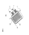
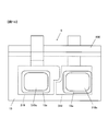
- FIG. 1 is a view showing an appearance of a power module according to the present invention.
- the power module 300 includes a power semiconductor unit that is transfer-molded so as to include a switching element, in a metal cylinder 1.
- the power module 300 is used in, for example, a power conversion device mounted on an electric vehicle such as an electric vehicle or a hybrid vehicle.
- a thick portion 301 in which a plurality of radiating fins 305 are erected and a thin portion 302 provided around the thick portion 301.
- the thin wall portion 302 is plastically deformed so that the heat radiating surface of the power semiconductor unit housed therein and the inner peripheral surface of the thick wall portion 301 are brought into close contact with each other.
- a large current terminal 3 and a signal terminal 4 provided on the power semiconductor unit protrude from one surface of the metal cylinder 1.
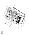
- FIG. 2 is an exploded perspective view of the power semiconductor unit 6, and FIG. 3 is a circuit diagram of the power semiconductor unit 6.
- IGBTs insulated gate bipolar transistors
- 155 and 157 and diodes 156 and 158 are provided as power semiconductor elements.
- two IGBTs 155 and 157 and two diodes 156 and 158 are provided in parallel, but only one of them is shown in the circuit diagram of FIG. 3 for the sake of simplicity.
- a DC positive electrode lead frame 315 and a first AC electrode lead frame 316 are arranged on substantially the same plane on one side across the power semiconductor element, and a second AC electrode lead frame 318 and DC are arranged on the other side.
- the negative electrode lead frame 319 is disposed on substantially the same plane.
- Each power semiconductor element has a flat plate-like structure, and each electrode is formed on the front and back surfaces.
- the collector electrode of the upper arm IGBT 155 and the cathode electrode of the upper arm diode 156 are fixed to the element fixing portion 322 of the DC positive electrode lead frame 315 by solder 160 which is a metal joined body.
- the collector electrode of the lower arm IGBT 157 and the cathode electrode of the lower arm diode 158 are fixed to the element fixing portion 322 of the first AC electrode lead frame 316 by solder 160 that is a metal joined body.
- solder whose main component is tin
- a solder whose main component is gold, silver or copper, or a brazing material or paste.
- the emitter electrode of the upper arm IGBT 155 and the anode electrode of the upper arm diode 156 are fixed to the element fixing portion 322 of the second AC electrode lead frame 318 by solder 160 which is a metal joined body.
- the emitter electrode of the lower arm IGBT 157 and the anode electrode of the lower arm diode 158 are fixed to the element fixing portion 322 of the DC negative electrode lead frame 319 by solder 160 which is a metal joined body.
- a silver sheet or a low-temperature sintered bonding material containing fine metal particles is used for the metal bonded body, and each power semiconductor element and the lead frame are bonded electrically and thermally. .
- the DC positive electrode lead frame 315 and the second AC electrode lead frame 318 are opposed substantially in parallel with each IGBT 155 and the diode 156 being power semiconductor elements interposed therebetween.
- the first AC electrode lead frame 316 and the DC negative electrode lead frame 319 face each other substantially in parallel so as to sandwich the IGBTs 157 and the diodes 158 that are power semiconductor elements.
- the first AC electrode lead frame 316 and the second AC electrode lead frame 318 are connected via an intermediate electrode 159. By connecting with the intermediate electrode 159, the upper arm circuit and the lower arm circuit are electrically connected to form an upper and lower arm series circuit as shown in FIG.
- the DC positive electrode wiring 315A is integrally formed with the DC positive electrode lead frame 315, and the DC positive electrode terminal 315B is formed at the tip of the DC positive electrode wiring 315A.
- the DC negative electrode wiring 319A is integrally formed with the DC negative electrode lead frame 319, and a DC negative electrode terminal 319B is formed at the tip of the DC negative electrode wiring 319A.
- An AC wiring 320 is integrally formed on the first AC electrode lead frame 316, and an AC terminal 321 is formed at the tip of the AC wiring 320.
- thermoplastic resin terminal block 600 is interposed between the DC positive electrode wiring 315A and the DC negative electrode wiring 319A.
- the direct current positive electrode wiring 315A and the direct current negative electrode wiring 319A extend so as to protrude from the metal cylinder 1 in a state of facing each other substantially in parallel.
- the signal terminals 4L and 4U are integrally formed with the thermoplastic resin terminal block 600, and extend so as to protrude from the metal tube 1 in the same direction as the DC positive electrode wiring 315A and the DC negative electrode wiring 319A. . Therefore, insulation between the direct current positive electrode wiring 315A and the direct current negative electrode wiring 319A and insulation between the signal wiring and each wiring board can be secured, and high-density wiring is possible.
- thermoplastic resin having heat resistance and insulating properties higher than the mold temperature of the transfer mold (for example, 180 ° C. or higher) is suitable, such as polyphenylene sulfide (PPS) or A liquid crystal polymer (LCP) or the like is used.
- PPS polyphenylene sulfide
- LCP liquid crystal polymer
- the direct current positive electrode wiring 315A and the direct current negative electrode wiring 319A are arranged so as to face each other substantially in parallel. That is, the current that instantaneously flows during the switching operation of the power semiconductor element is configured to flow in the opposite direction between the direct current positive electrode wiring 315A and the direct current negative electrode wiring 319A arranged so as to face each other. Were offset each other. Thereby, the inductance can be reduced.
- FIG. 4A consider a state in which the lower arm diode 158 is conducting in the forward bias state.
- the upper arm IGBT 155 is turned on, the lower arm diode 158 is reverse-biased, and a recovery current caused by carrier movement passes through the upper and lower arms.
- the recovery current 100 shown in FIG. 4B flows through the electrode lead frames 315, 316, 318, and 319.
- the recovery current 100 passes through a DC positive terminal 315B arranged in parallel with the DC negative terminal 319B, and then flows through a loop-shaped path formed by the electrode lead frames 315, 316, 318, 319. Then, the current flows again as shown by the solid line through the DC positive terminal 315B arranged in parallel with the DC negative terminal 319B.
- an eddy current 101 flows in the heat dissipation base 307. Due to the magnetic field canceling effect by the eddy current 101, the wiring inductance 102 in the loop-shaped path is reduced. Note that the closer the current path is to the loop shape, the greater the inductance reduction effect.
- the loop-shaped current path flows through a path close to the terminal side of the electrode lead frame 315 as shown by a dotted line, passes through the semiconductor element, and is far from the terminal side of the electrode lead frame 318 as shown by a solid line. Flowing. After that, it flows through a path farther from the terminal side of the electrode lead frame 316 as shown by a dotted line, passes again through the semiconductor element, and flows through a path closer to the terminal side of the electrode lead frame 319 as shown by a solid line.
- a loop-shaped circuit is formed by passing a path closer to or farther from the DC positive terminal 315B and the DC negative terminal 319B, and the heat dissipation base 307 is formed by the recovery current 100 flowing through the loop-shaped circuit.
- Eddy current 101 flows through By canceling out the magnetic field of the eddy current 101 and the magnetic field of the recovery current 100, there is an effect of reducing reluctance.
- FIG. 5 is a control block diagram of a hybrid vehicle equipped with an inverter equipped with the power module 300 shown in FIG.
- the hybrid vehicle (HEV) 110 includes two vehicle drive systems. One is an engine drive system using the engine 120 as a power source, and the other is a rotating electrical machine drive system using motor generators 192 and 194 as a power source.
- the motor generator is a motor that functions as a motor or functions as a generator under control.
- the front part of the vehicle body has a pair of front wheels 112, and a front wheel axle 114 connected to the front wheels 112 is connected to the output side of a differential gear (DEF) 116.
- a transmission (T / M) 118 is connected to the input side of the front wheel side DEF 116.
- the output side of the motor generator (MG1) 192 is connected to the input side of the transmission 118.
- the output side of the engine (ENG) 120 or the output side of the motor generator (MG2) 194 is connected to the input side of the motor generator 192 via the power distribution mechanism 122.
- Motor generators 192 and 194 and power distribution mechanism 122 are housed inside the casing of transmission 118.
- induction machine or a synchronous machine is used for the motor generators 192 and 194
- a synchronous machine having a permanent magnet on the rotor is used, which is efficient in this embodiment.
- the AC power supplied to the stator windings of the stators of the induction machine and the synchronous machine is controlled by the inverter circuit units 140 and 142 so that the motor generators 192 and 194 operate as motors or generators and their characteristics. Is controlled.
- a battery 136 is connected to the inverter circuit units 140 and 142, and power can be exchanged with the inverter circuit units 140 and 142.
- the HEV 110 includes a first motor generator unit composed of a motor generator 192 and an inverter circuit unit 140 and a second motor generator unit composed of a motor generator 194 and an inverter circuit unit 142, which are selectively used according to the operating state. ing. That is, in the situation where the vehicle is driven by the power from the engine 120, when assisting the driving torque of the vehicle, the second motor generator unit is operated by the power of the engine 120 as a power generation unit to generate power, and the power generation The first motor generator unit is operated as an electric unit by the electric power obtained by the above. Further, when assisting the vehicle speed in the same situation, the first motor generator unit is operated by the power of the engine 120 as a power generation unit to generate power, and the second motor generator unit is generated by the electric power obtained by the power generation. Operate as an electric unit.
- the vehicle can be driven only by the power of the motor generator 192.
- the battery 136 can be charged by operating the first motor generator unit or the second motor generator unit as a power generation unit by the power of the engine 120 or the power from the wheels to generate power.
- the battery 136 is also used as a power source for driving an auxiliary motor 195.
- the auxiliary machine include a motor for driving a compressor of an air conditioner or a motor for driving a hydraulic pump for control.
- the DC power supplied from the battery 136 to the inverter circuit unit 43 is an inverter circuit unit for the auxiliary machine. 43 is converted into AC power and supplied to the motor 195.
- the auxiliary inverter circuit unit 43 has the same function as the inverter circuit units 140 and 142, and controls the phase, frequency, and power of alternating current supplied to the motor 195.
- the motor 195 generates torque by supplying AC power having a leading phase with respect to the rotation of the rotor of the motor 195.
- the motor 195 acts as a generator, and the motor 195 is operated in a regenerative braking state.
- the control function of the inverter circuit unit 43 for auxiliary equipment is the same as the control function of the inverter circuit units 140 and 142. Since the capacity of the motor 195 is smaller than the capacity of the motor generators 192 and 194, the maximum conversion power of the inverter circuit unit 43 for the auxiliary machine is smaller than the inverter circuit parts 140 and 142, but the circuit configuration of the inverter circuit unit 43 for the auxiliary machine Is basically the same as the circuit configuration of the inverter circuit units 140 and 142.
- the constant voltage power supply is omitted.
- Each control circuit and various sensors operate with electric power from a constant voltage power source (not shown).
- This constant voltage power source is, for example, a 14 volt power source, and includes a 14 volt system such as a lead battery, and in some cases a 24 volt system battery.
- the constant voltage power source one of the positive electrode and the negative electrode is connected to the vehicle body, and the vehicle body is used as a power supply conductor of the constant voltage power source.
- the inverter circuit sections 140, 142, and 43 and the capacitor module 500 are in an electrical close relationship. Furthermore, there is a common point that measures against heat generation are necessary. It is also desired to make the volume of the device as small as possible. From these points, the power conversion device 200 described in detail below includes the inverter circuit units 140, 142, and 43 and the capacitor module 500 in the housing of the power conversion device 200. With this configuration, it is possible to reduce the size, and there is an effect that the number of harnesses can be reduced and radiation noise can be reduced. This effect leads to downsizing or improved reliability. It also leads to improved productivity.
- connection circuit between the capacitor module 500 and the inverter circuit units 140, 142, and 43 is shortened, or a structure described below is possible, whereby inductance can be reduced and, as a result, spike voltage can be reduced. Furthermore, the structure described below can reduce heat generation and improve heat dissipation efficiency.
- FIG. 6 is a circuit diagram of the power conversion device 200.
- the power conversion apparatus 200 includes inverter circuit units 140 and 142, an auxiliary inverter circuit unit 43, and a capacitor module 500.
- the inverter circuit units 140 and 142 include a plurality of power modules 300 having a double-sided cooling structure, and a three-phase bridge circuit is configured by connecting them. In the example shown in FIG. 6, three power modules 300 are provided. When the current capacity is large, the power modules 300 are further connected in parallel, and these parallel connections are made corresponding to the respective phases of the three-phase inverter circuit, so that an increase in the current capacity can be accommodated. In addition, it is possible to cope with an increase in current capacity by connecting semiconductor elements built in the power module 300 in parallel.
- Each inverter circuit unit 140 or 142 is driven and controlled by two driver circuits provided in the control unit.
- the two driver circuits are displayed together as a driver circuit 174.
- Each driver circuit is controlled by a control circuit 172.
- the control circuit 172 generates a switching signal for controlling the switching timing of the power semiconductor element.
- the basic circuit configuration of the inverter circuit unit 140 and the inverter circuit unit 142 is the same, and the control method and operation are basically the same.
- the inverter circuit unit 140 will be described as an example.
- the inverter circuit unit 140 includes a three-phase bridge circuit as a basic configuration. Specifically, the inverter circuit unit 140 operates as a U phase (indicated by a symbol U1), a V phase (indicated by a symbol V1), or a W phase (indicated by a symbol W1). Each of the arm circuits is connected in parallel to the positive and negative conductors that transmit DC power.
- the arm circuits operating as the U-phase, V-phase, and W-phase of the inverter circuit unit 142 are denoted by reference numerals U2, V2, and W2, as in the case of the inverter circuit unit 140.
- the arm circuit of each phase is composed of an upper and lower arm series circuit in which an upper arm circuit and a lower arm circuit are connected in series.
- the upper arm circuit of each phase is connected to the positive conductor, and the lower arm circuit of each phase is connected to the negative conductor.
- AC power is generated at the connection between the upper arm circuit and the lower arm circuit.
- a connection portion between the upper arm circuit and the lower arm circuit of each upper and lower arm series circuit is connected to an AC terminal 321 of each power module 300.
- the AC terminal 321 of each power module 300 is connected to the AC output terminal of the power converter 200, and the generated AC power is supplied to the stator winding of the motor generator 192 or 194. Since each power module 300 of each phase has basically the same structure and basically the same operation, the power module U1 that is the U-phase power module 300 will be described as a representative.
- the upper arm circuit includes an upper arm IGBT 155 and an upper arm diode 156 as power semiconductor elements for switching.
- the lower arm circuit includes a lower arm IGBT 157 and a lower arm diode 158 as power semiconductor elements for switching.
- the DC positive terminal 315 and the DC negative terminal 319 of each upper and lower arm series circuit are respectively connected to the capacitor connecting DC terminals of the capacitor module 500, and the AC power generated at the AC terminal 321 is supplied to the motor generators 192 and 194.
- the IGBTs 155 and 157 receive a drive signal output from one or the other of the two driver circuits constituting the driver circuit 174 and perform a switching operation to convert the DC power supplied from the battery 136 into three-phase AC power.
- the converted electric power is supplied to the stator winding of the motor generator 192. Since the V phase and the W phase have substantially the same circuit configuration as the U phase, the reference numerals 155, 157, 156, and 158 are omitted.
- the power module 300 of the inverter circuit unit 142 has the same configuration as that of the inverter circuit unit 140, and the inverter circuit unit 43 for auxiliary machines has the same configuration as the inverter circuit unit 142. Here, Description is omitted.
- the power semiconductor element for switching will be described using the upper arm IGBT 155 and the lower arm IGBT 157.
- the upper arm IGBT 155 and the lower arm IGBT 157 include a collector electrode, an emitter electrode (signal emitter electrode terminal), and a gate electrode (gate electrode terminal).
- An upper arm diode 156 and a lower arm diode 166 are electrically connected between the collector electrode and the emitter electrode of the upper arm IGBT 155 and the lower arm IGBT 157 as shown in the figure.
- the upper arm diode 156 and the lower arm diode 158 include two electrodes, a cathode electrode and an anode electrode.
- the cathode electrodes of the diodes 156 and 158 are the collector electrodes of the IGBTs 155 and 157 and the anode electrode is the emitter of the IGBTs 155 and 157 so that the direction from the emitter electrode of the upper arm IGBT 155 and the lower arm IGBT 157 toward the collector electrode is the forward direction.
- Each is electrically connected to the electrode.
- a MOSFET metal oxide semiconductor field effect transistor
- the upper arm diode 156 and the lower arm diode 158 are not necessary.
- the control circuit 172 generates a timing signal for controlling the switching timing of the upper arm IGBT 155 and the lower arm IGBT 157 based on input information from a control device or a sensor (for example, a current sensor 180) on the vehicle side. .
- the driver circuit 174 generates a drive signal for switching the upper arm IGBT 155 and the lower arm IGBT 157 based on the timing signal output from the control circuit 172.
- the control circuit 172 includes a microcomputer (hereinafter referred to as a “microcomputer”) for calculating the switching timing of the upper arm IGBT 155 and the lower arm IGBT 157.
- a microcomputer for calculating the switching timing of the upper arm IGBT 155 and the lower arm IGBT 157.
- the target torque value required for the motor generator 192 the current value supplied from the upper and lower arm series circuit to the stator winding of the motor generator 192, and the magnetic pole position of the rotor of the motor generator 192 are input information. Entered.
- the target torque value is based on a command signal output from a host controller (not shown).
- the current value is detected based on the detection signal output from the current sensor 180.
- the magnetic pole position is detected based on a detection signal output from a rotating magnetic pole sensor (not shown) provided in the motor generator 192.
- the case of detecting the current values of three phases will be described as an example, but the current values of two phases may be detected.
- the microcomputer in the control circuit 172 calculates the d-axis and q-axis current command values of the motor generator 192 based on the target torque value, and the calculated d-axis and q-axis current command values and the detected d-axis.
- the voltage command value for the d-axis and q-axis is calculated based on the difference from the current value for q and q-axis.
- the microcomputer converts the calculated d-axis and q-axis voltage command values into U-phase, V-phase, and W-phase voltage command values based on the detected magnetic pole positions.
- the microcomputer generates a pulse-like modulated wave based on the comparison between the fundamental wave (sine wave) and the carrier wave (triangular wave) based on the voltage command values of the U-phase, V-phase, and W-phase, and the generated modulation
- the wave is output to the driver circuit 174 as a PWM (pulse width modulation) signal.
- the driver circuit 174 When driving the lower arm, the driver circuit 174 amplifies the PWM signal and outputs it as a drive signal to the gate electrode of the corresponding lower arm IGBT 157.
- the driver circuit 174 when driving the upper arm, the driver circuit 174 amplifies the PWM signal after shifting the level of the reference potential of the PWM signal to the level of the reference potential of the upper arm, and uses this as a drive signal. Output to the gate electrode of the upper arm IGBT 155.
- the upper arm IGBT 155 and the lower arm IGBT 157 perform a switching operation based on the input drive signal.
- control unit detects abnormalities (overcurrent, overvoltage, overtemperature, etc.) and protects the upper and lower arm series circuit. For this reason, sensing information is input to the control unit. For example, information on the current flowing through the emitter electrodes of the upper arm IGBT 155 and the lower arm IGBT 157 is input to the corresponding driver circuit 174 from the signal emitter electrode terminal of each arm. As a result, the driver circuit 174 detects overcurrent. When the overcurrent is detected, the driver circuit 174 stops the switching operation of the corresponding upper arm IGBT 155 and lower arm IGBT 157, and the corresponding upper arm IGBT 155 and lower arm IGBT 157. Protects against overcurrent.
- abnormalities overcurrent, overvoltage, overtemperature, etc.
- Temperature information of the upper and lower arm series circuit is input to the microcomputer from a temperature sensor (not shown) provided in the upper and lower arm series circuit. Further, voltage information on the DC positive side of the upper and lower arm series circuit is input to the microcomputer. The microcomputer performs over temperature detection and over voltage detection based on the information, and when an over temperature or over voltage is detected, the switching operation of all the upper arm IGBTs 155 and the lower arm IGBTs 157 is stopped, and the upper and lower arms are connected in series. Protect the circuit from over temperature or over voltage.
- the conduction and cut-off operations of the upper arm IGBT 155 and the lower arm IGBT 157 of the inverter circuit unit 140 are switched in a certain order, and the current generated in the stator winding of the motor generator 192 at this switching is a circuit including diodes 156 and 158. Flowing.
- one upper and lower arm series circuit is provided for each phase of the inverter circuit unit 140. As described above, the output of each phase of the three-phase AC output to the motor generator is provided.
- the generated circuit may be a power conversion device having a circuit configuration in which two upper and lower arm series circuits are connected in parallel to each phase.
- the DC terminals 138 (see FIG. 5) provided in the inverter circuit units 140 and 142 are connected to a laminated electrode lead frame 700 including a positive electrode lead frame and a negative electrode lead frame.
- the laminated electrode lead frame 700 has a three-layer structure in which an insulating sheet (not shown) is sandwiched between a positive electrode-side electrode lead frame 702 and a negative-electrode-side electrode lead frame 704 made of a conductive plate material wide in the arrangement direction of the power modules 300.
- a laminated wiring board is configured.
- the positive electrode lead frame 702 and the negative electrode lead frame 704 of the multilayer electrode lead frame 700 are connected to the positive electrode lead frame 507 and the negative electrode lead frame 505 of the multilayer wiring board 501 provided in the capacitor module 500, respectively.
- the positive electrode lead frame 507 and the negative electrode lead frame 505 are also made of a conductive plate material that is wide in the power module arrangement direction, and constitute a three-layer laminated wiring board with an insulating sheet 517 (not shown) sandwiched therebetween.
- the capacitor module 500 has a plurality of capacitor cells 514 connected in parallel.
- the positive electrode side of the capacitor cell 514 is connected to the positive electrode lead frame 507, and the negative electrode side of the capacitor cell 514 is connected to the negative electrode lead frame 505.
- Capacitor module 500 constitutes a smoothing circuit for suppressing fluctuations in DC voltage caused by switching operations of upper arm IGBT 155 and lower arm IGBT 157.
- the multilayer wiring board 501 of the capacitor module 500 is connected to the input multilayer wiring board 230 connected to the DC connector 138 of the power converter 200.
- the input laminated wiring board 230 is also connected to an inverter device in the inverter circuit unit 43 for auxiliary machines.
- a noise filter is provided between the input multilayer wiring board 230 and the multilayer wiring board 501.
- the noise filter includes two capacitors that connect the ground terminal of the housing 12 and each DC power line, and constitutes a Y capacitor for common mode noise countermeasures.
- the capacitor module 500 includes a terminal (not shown) connected to the DC connector 138 for receiving DC power from the DC power supply 136 and a terminal connected to the inverter circuit 140 or the inverter circuit 142 separately. Thereby, the adverse effect of noise generated by the inverter circuit 140 or the inverter circuit 142 on the DC power source 136 is reduced. This configuration enhances the smoothing effect.
- the inductance for the current flowing through the upper and lower arm series circuit of each power module 300 is reduced, The voltage that jumps up due to sudden change is reduced.
- FIG. 7 is a perspective view showing the appearance of the power converter 200
- FIG. 8 is a cross-sectional view taken along the line AA of FIG. 7
- FIG. 9 is a case where the upper case 10 and the AC connector are removed from the power converter 200 shown in FIG.
- FIG. 10 is a cross-sectional view taken along the line BB of FIG.
- the external appearance of the power change device 200 according to the present embodiment is as follows.
- the housing 12 has a substantially rectangular top or bottom surface, the upper case 10 provided on one of the outer circumferences on the short side of the housing 12, and the housing 12.
- the lower case 16 for closing the lower opening is fixed and formed.
- An AC terminal case 17 provided with an AC terminal 18 is provided on the outer periphery on the long side of the power change device 200.
- the AC terminal 18 electrically connects the power module 300 and the motor generators 192 and 194 and transmits an AC current output from the power module 300 to the motor generators 192 and 194.
- the connector 21 is connected to a control circuit board 20 (see FIG. 8) built in the housing 12 and transmits various signals from the outside to the control circuit board 20.
- the DC negative electrode side connection terminal 510 and the DC positive electrode side connection terminal 512 electrically connect the battery 136 and the capacitor module 500.
- a cooling jacket 19 ⁇ / b> A having a water channel is formed in the middle of the housing 12.
- a control circuit board 20 on which a control circuit 172 is mounted and a drive circuit board 22 on which a driver circuit 174 is mounted are disposed in the space above the cooling jacket 19A.
- a capacitor module 500 is arranged in a space below the cooling jacket 19A.
- the capacitor module 500 is provided with a plurality of capacitor cells 504.
- the cooling jacket 19A is formed with a water channel 19 through which cooling water flows, and a plurality of openings 400 and 402 for inserting and arranging the power module 300 in the water channel are formed on the water channel as shown in FIG. ing.
- the power module 300 is inserted into the water channel through these openings 400 and 402 and fixed to the housing 12. 1 is immersed in the cooling water, and the power module 300 is cooled by the cooling water.
- FIG. 10 is a cross-sectional view taken along the line BB of FIG. 8, and shows a portion of the cooling jacket 19A of the housing 12 in which the water channel 19 is formed.
- the cooling water flowing into the water channel 19 from the cooling water inlet 13 flows through the meandering water channel 19 as indicated by an arrow 421 and is discharged from the cooling water outlet 14.
- six power modules 300 are arranged along the flow of the cooling water.
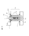
- FIG. 11 is a cross-sectional view showing the power module 300 arranged in the water channel.
- the cooling jacket 19 ⁇ / b> A having the cooling water channel 19 is formed inside the housing 12.
- a back cover 420 for covering the bottom surface side of the water channel 19 is attached to the bottom surface side of the cooling jacket 19A.
- the lower end portion of the metal cylinder 1 protrudes downward from the water channel 19 of the cooling jacket 19A and is housed in a recess 420a formed in the back cover 420.
- the gap between the back cover 420 and the cooling jacket 19A and the gap between the flange 304B of the power module 300 and the cooling jacket 19A are sealed with seals 800 and 801.
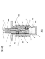
- FIG. 12 is a schematic cross-sectional view for explaining the power module 300 in the present embodiment.
- FIG. 12 shows a cross section of a portion where the power semiconductor element 5 is provided, for example, a cross section of a portion where the IGBT 155 of FIG. 2 is provided.
- the IGBT 155 and the diode 156 are juxtaposed in the extending direction of the electrode lead frame.
- the illustration of the diode is omitted, and the IGBT 155 is illustrated as the power semiconductor element 5.
- Reference numerals 7 and 8 denote electrode lead frames.
- Reference numeral 3 denotes a large current terminal formed integrally with the electrode lead frame, and corresponds to the DC positive terminal 315B, the DC negative terminal 319B, and the AC terminal 321 shown in FIG.
- the signal terminal 4 corresponds to the signal terminals 4L and 4U in FIG. Since the electrode lead frame is required to have high thermal conductivity and high strength, it is desirable to use copper as the main component, but it is also possible to use a material containing aluminum as the main component.
- the power module 300 is a unit in which the power semiconductor unit 6 described above is accommodated in the metal cylinder 1, and the gap between the power semiconductor unit 6 and the metal cylinder 1 is filled with potting resin 2.
- the power semiconductor unit 6 is obtained by transfer molding the power semiconductor element 5, the electrode lead frames 7, 8, etc. with the sealing material 13, and is housed in a thick portion 301 in the metal cylinder 1.
- the power semiconductor element 5 has electrodes formed on the front and back surfaces of the chip.
- An electrode lead frame 7 is joined to the back side of the power semiconductor element 5, and an electrode lead frame 8 is joined to the front side of the power semiconductor element 5. Yes.
- a control electrode (IGBT gate electrode) provided on the surface side of the power semiconductor element 5 is connected to the signal terminal 4 by an aluminum wire bonding 11.
- the signal terminal 4 is insert-molded in the terminal block 600.
- the terminal block 600 is made of a thermoplastic resin such as polyphenylene sulfide (PPS).
- PPS polyphenylene sulfide
- the electrode lead frames 7 and 8 are formed by press punching, and the end surface facing the metal tube 1 is chamfered.
- An insulating sheet 10 for maintaining electrical insulation is disposed between the metal tube 1 and the electrode lead frames 7 and 8.
- a thermosetting resin is used for the insulating sheet 10, and the insulating sheet 10 and the heat radiating surface are bonded by pressure-bonding the insulating sheet 10 before curing to the heat radiating surface side of the electrode lead frames 7 and 8. The formation of voids (fine cavities) between them is prevented.
- FIGS. 13A and 13B are enlarged views of the regions indicated by reference signs C1 and C2.
- a step is likely to be formed between the heat radiation surface of the electrode lead frames 7 and 8 and the sealing material surface 13b, and voids are likely to occur at the step portion. Therefore, in this embodiment, when the heat radiating surface 7b protrudes from the sealing material surface 13b as shown in FIG. 13A, the end surface of the electrode lead frame 7 is provided with the inclined surface 7a by chamfering. It was made to form. Conversely, as shown in FIG.
- FIG. 14 is a diagram showing a method of manufacturing a power semiconductor unit by transfer molding.
- the IGBT 157, the diode 158, and the electrode lead frames 316 and 319 in FIG. 2 are shown as an example.
- the IGBT 157 has an emitter electrode and a gate electrode formed on the upper side (chip surface side) in the drawing, and a collector electrode formed on the lower side (chip rear surface side) in the drawing.
- the solder sheet 160a is placed on the element fixing portion 322 of the collector-side electrode lead frame 316, and the IGBT 157 and the diode 158 are placed on the solder sheet 160a. Further, the solder sheet 160a is placed on the IGBT 157 and the diode 158, and the emitter-side electrode lead frame 319 is placed thereon.
- a terminal block 600 made of a thermoplastic resin in which the signal terminal 4 is insert-molded is inserted between terminals (large current terminals 3 in FIG. 12) extending from the collector-side and emitter-side electrode lead frames 316 and 319. Then, the gate electrode of the IGBT 157 and the signal terminal 4 are electrically connected by the aluminum wire bonding 11.
- a flexible release sheet 27 is disposed on the lower mold 26b of the transfer mold dies 26a and 26b, and the mold is formed on the release sheet 27 in the step of FIG. 4B.
- a lead frame structure is placed.
- the collector-side electrode lead frame 316 is disposed on the release sheet 27 side.
- the upper mold 26a and the lower mold 26b of the mold are clamped, and transfer molding is performed under a pressurizing condition of a mold temperature of 175 ° C. and a pressure of 10 MPa.
- the dimensions of the mold and the thickness of the release sheet 27 are set so that the electrode lead frame 316 sinks into the release sheet 27 when the mold is clamped. That is, the mold dimensions are set in consideration of the height dimension variation when forming the lead frame structure, and the electrode lead frame 316 sinks into the release sheet 27 to a predetermined amount (for example, about 25 ⁇ m). Thus, the thickness dimension of the release sheet 27 is selected.
- FIG. 14D is a view showing the power semiconductor unit 6 after the transfer mold dies 26a and 26b are removed from the state of FIG. 14C and the release sheet 27 is removed.
- the tip portion of the electrode lead frame having the largest height is in contact with the upper die 26a, and in the other regions, it is between the upper die 26a. There is a gap.
- the sealing material 13 wraps around the heat radiating surface 319s of the electrode lead frame 319, as indicated by reference numeral D1 in FIG.
- the shape of the sealing material edge portion where the sealing material 13 wraps around tends to be an inversely tapered shape with respect to the heat radiation surface 319 s of the electrode lead frame 319 due to surface tension and the like.
- the sealing material 13 may be removed by machining, or may be removed by laser processing.
- the laser irradiation range S1 is set to be inside the outer edge of the electrode lead frame 319 as shown in FIG. The reason is that when the laser light is incident on the outer side of the outer peripheral edge of the electrode lead frame 319, the sealing material 13 is deeply cut, and a steep step is generated in that portion. And by changing the irradiation intensity of the laser, the edge portion of the enclosing sealing material 13 turned into the inclined surface 13a as shown in FIG.
- FIG. 16 is a plan view of the power semiconductor unit 6 after forming the inclined surface.
- the sealing material 13 wraps around the heat radiation surfaces 318 s and 319 s, and the central portion is exposed from the sealing material 13.
- the edge portion of the sealing material 13 in contact with the periphery of the exposed regions 318A and 319A has a step shape as shown in FIG. 14 (d).
- the inclined surface 13a is exposed by forming the inclined surface by laser irradiation or the like described above. It is formed so as to surround 318A and 319A.
- the power semiconductor unit 6 shown in FIG. 12 As shown in FIG. 12, the power semiconductor unit 6 shown in FIG. At that time, the insulating sheet 10 is disposed between the front and back surfaces of the power semiconductor unit 6 and the inner peripheral surface of the metal cylinder 1. The insulating sheet 10 is pressure-bonded to both the front and back surfaces of the power semiconductor unit 6 as will be described later. At that time, voids are likely to occur in the regions indicated by reference numerals D1 and D2 in FIG.
- the inclined surface 13a described above is formed in the edge of the sealing material in the region D1.
- the end portion of the electrode lead frame 316 is chamfered to form an inclined surface 316c (corresponding to the inclined surface 7a of the electrode lead frame 7 in FIG. 13), as shown in FIG. 14 (c).
- transfer molding was performed with the electrode lead frame 316 submerged in the release sheet 27.
- FIG. 17 is an enlarged view of the regions D1 and D2 when the above-described inclined surface processing is performed, and shows an example of the inclined surfaces 13a and 316c formed at the step portion between the heat radiation surface and the sealing material 13. It is. Looking at the protruding relationship between the heat radiation surface and the surface 13b of the sealing material 13, the sealing material surface 13b protrudes in the region D1 as shown in FIG. 17A, and conversely, in FIG. In the region D2, the heat radiation surface 316s of the electrode lead frame 316 protrudes. In the case of the region D2, since a part of the inclined surface 316c obtained by chamfering is sunk in the release sheet 27 as shown in FIG. 14C, the sealing material 13 has a part on the inclined surface 316c. It is shaped to ride.
- the slope shape of the step is similar in both cases.
- the intersection of the projecting surface and the inclined surface is Q, and the intersection of the inclined surface and the recessed surface is P
- the inclination ⁇ of the straight line L1 passing through the points P and Q is the average of the inclined surface PQ. It can be said that it shows a general inclination.
- the inclined surface PQ refers to a curved surface from the point P to the point Q, and is a substantially inclined surface of the step structure.
- the inclined surface in the region D2 is the surface of the release sheet 27 and the chamfered portion of the electrode lead frame 316 when the electrode lead frame 316 is submerged in the release sheet 27 (the inclined surface 7a in FIG. 13A). Therefore, the inclined surface of the step structure cannot be strictly a plane as indicated by the straight line L1. On the other hand, in the case of the inclined surface 13a of the sealing material 13 shown in FIG. 17A, a flat inclined surface as shown by a straight line L1 can be used.
- FIG. 18 is a diagram for explaining the effect when the flat inclined surface PQ is formed.
- the insulating sheet 10 is pressure-bonded to both the front and back surfaces of the power semiconductor unit 6, as described above, voids are likely to occur during the pressure bonding. Although details will be described later, the insulating sheet 10 has flexibility and fluidity during the pressure bonding. Therefore, when pressure is applied from above, a part of the insulating sheet 10 is deformed without a gap following the surface shape of the power semiconductor unit 6.
- FIG. 19 shows a case where an inclined surface is not formed in the step portion of the sealing material 13 as a comparative example. Since the pocket-shaped space is formed in the edge portion (the portion indicated by the symbol C) of the sealing material 13 that wraps around the heat dissipation surface of the electrode lead frame 319, the insulating sheet 10 can be used even when pressure bonding is performed. It is very difficult to enter the space without any gaps, and voids are generated in that portion.
- the deformable insulating sheet 10 is pressed against the inclined surface PQ by pressing, but the pressure P1 depends on the angle ⁇ of the inclined surface PQ.
- the magnitude of the pressure P1 can be considered as a component perpendicular to the inclined surface PQ of the applied pressure P0, and becomes larger as the angle ⁇ is smaller. Since this pressure P1 acts so as to compress the void, a larger one is preferable.
- the pressure P0 is about 1 MPa, and in order to suppress the generation of voids, it is preferable that a pressure equal to or more than 1/3 of the pressure P1 acts as the pressure on the inclined surface PQ.
- the angle ⁇ of the inclined surface PQ it is preferable to set the angle ⁇ of the inclined surface PQ to 70 deg or less.
- the angle between the inclined surface PQ and the adjacent heat radiating surface or sealant surface is an obtuse angle, and the obtuse angle is set to 110 degrees or more and less than 180 degrees.
- the inclined surface PQ is curved, and the inclination angle is an angle ⁇ 1 in the vicinity of the point P1, and an angle ⁇ 2 (> ⁇ 1) in the vicinity of the point Q1.
- the planar inclined surface PQ is described in FIG. 18, it is more preferable to use a curved inclined surface having angles ⁇ 1 and ⁇ 2 as shown in FIG. With such a shape, the insulating sheet 10 flows with a pressure applied perpendicularly to the heat radiating surface 319s of the electrode lead frame 319, and the effect of flowing the void of the heat radiating surface 319s to the side is great.
- the void can be compressed by increasing the pressure applied when the insulating sheet 10 is crimped.
- the semiconductor element may be destroyed. Therefore, it is desirable that the semiconductor element can be compressed to a void of about 7.5 ⁇ m or less without affecting the insulation performance.
- FIG. 20 is a view showing an example of the insulating sheet 10, and the insulating sheet 10 in FIG. 20 (a) shows an example of a three-layer structure.
- the high thermal conductive layer 37 at the center is obtained by filling a resin component with an alumina filler that is an insulating inorganic material having a thermal conductivity of 5 W / mK or more at a volume fraction of 50% to 90%.
- an insulating inorganic material having a thermal conductivity of 5 W / mK or more aluminum nitride, boron nitride or the like can be used in addition to the alumina filler.
- the high adhesion layer 38 provided on both the front and back sides of the high thermal conductive layer 37 is a resin component having a volume fraction of more than 50%.
- an epoxy-modified polyamideimide resin is used as the resin component, but a thermosetting resin such as an epoxy resin or a bismaleimide resin may be used.
- the high thermal conductive layer may be formed by a plurality of layers, or the highly adhesive layer may be formed by a plurality of layers.
- the metal tube side to which the insulating sheet is crimped may be alumite-treated or roughened to improve adhesion, and the high heat conductive layer may be directly bonded to the metal tube side.
- the metal tube side to which the insulating sheet is crimped may be alumite-treated or roughened to improve adhesion, and the high heat conductive layer may be directly bonded to the metal tube side.
- FIG. 20B is a schematic diagram showing an example of the high adhesion layer 38 in an enlarged manner.
- the high adhesion layer 38 improves adhesion by increasing the resin component to a volume fraction of more than 50%.
- a silicone resin having an average particle diameter of about 1 ⁇ m is added to a matrix resin 35 such as an epoxy-modified polyamideimide resin.
- a matrix resin 35 such as an epoxy-modified polyamideimide resin.
- the insulating sheet 10 disposed between the power semiconductor unit 6 and the metal tube 1 has a thermal conductivity of 3 W / mK or more, a dielectric breakdown voltage of 20 kV / mm or more, and a sealing material.
- a material having an adhesive strength of 10 MPa or more with respect to the lead frame and the metal cylinder 1 is desirable. If the thermal conductivity is 3 W / mK or more, sufficient heat dissipation can be obtained even when the thickness of the insulating sheet 10 is 100 ⁇ m or more in order to ensure insulation reliability.
- the adhesive strength with respect to the metal cylinder 1 is 10 MPa or more, the adhesive force can be made higher than the stress generated in the temperature cycle, and the adhesion reliability is increased.
- the high thermal conductive layer 37 includes 50% or more of a volume fraction of alumina filler, which is an insulating and high thermal conductivity inorganic material. I made it.
- the adhesive strength of the high thermal conductive layer 37 is reduced. Therefore, the high thermal conductive layer 37 and the high adhesion layer 38 in which the resin component has a volume fraction of more than 50% are multilayered, and the high adhesion layer 38 is disposed on the side in contact with the metal cylinder 1 and the power semiconductor unit 6. did. That is, a multilayer structure as shown in FIG. As a result, it was possible to achieve both a high thermal conductivity of 3 W / mK or higher (in this embodiment, a thermal conductivity of 5 W / mK) and a high adhesive strength of 10 MPa or higher.
- a ceramic plate may be used as the above-described high thermal conductive layer 37, and insulation reliability can be further improved.
- the high thermal conductive layer 37 is flexible, so that the power semiconductor 6 and the metal cylinder 1 It is excellent in terms of followability to the surface shape.
- the uncured transfer mold sealing material contains a release agent such as polyethylene and stearic acid.
- This release agent is solid and non-sticky at room temperature, but becomes liquid at 90 ° C. or higher.
- the release agent that has become liquid has a lower solubility parameter than the epoxy resin that is the base resin of the sealing material, so that it floats to the surface when the sealing material is cured and improves the mold separation between the transfer mold and the sealing material. I am doing. Therefore, the adhesiveness of the adhesive to the sealing material that has been transfer molded is generally poor due to the raised release agent.
- the adhesive is improved by removing the release agent by UV cleaning, plasma cleaning, laser irradiation, polishing, or the like.
- the present inventors pay attention to a silicone resin having a solubility parameter close to that of the mold release agent, and form a high adhesion layer 38 containing the silicone resin 36 as shown in FIG. It was found that high adhesion can be achieved without a process. However, since the silicone resin has a low elastic modulus, there is a problem that the adhesive strength is lowered. In view of this, an investigation was made using an adhesive having a microphase separation structure in which a fine silicone resin is dispersed in a matrix resin having a high elastic modulus.
- the insulating sheet 10 has a three-layer structure in which the high thermal conductive layer 37 is sandwiched between the high adhesion layers 38, so that the insulating sheet 10 having high thermal conductivity and adhesion can be obtained. We were able to. For this reason, after the insulating sheet is cured, it is possible to maintain the adhesion of the insulating sheet 10 without maintaining the clamping pressure as described in Patent Document 1.
- FIG. 21 is a diagram illustrating a method for manufacturing a power module.
- the insulating sheet 10 is crimped.
- the release sheet is affixed on both front and back surfaces of the insulating sheet 10 shown in FIG. 20 from the viewpoint of workability, one side of the insulating sheet 10 (on the power semiconductor unit 6) Leave the release sheet on the non-opposing surface).
- pressure bonding is performed for 1 minute under conditions of a temperature of 130 ° C., a pressure of 1 MPa, and a pressure of 10 kPa.
- the first crimping is a temporary crimping operation for fixing the insulating sheet 10 to both the front and back surfaces of the power semiconductor unit 6 so that the power semiconductor unit 6 and the insulating sheet 10 can be easily inserted into the metal cylinder 1.
- the resin component contained in is not yet completely solidified. Specifically, the degree of cure of the resin component is about 80% or less. In order to achieve such a state, in the crimping operation of FIG. 21A, crimping is performed within 15 minutes under a temperature condition of 140 ° C. or less, a pressure condition of 2 MPa or less, and a pressure condition of 10 kPa or less. You can do that.
- the power semiconductor unit 6 having the insulating sheet 10 bonded to both the front and back surfaces is inserted into the metal cylinder 1.
- the thin wall portion 302 is plastically deformed by pressurizing the thick wall portion 301 of the metal tube 1 using a vacuum press machine, and the insulating sheet 10 and the metal tube 1 are pressure bonded.
- the conditions of the pressure bonding operation at this time were a temperature of 130 ° C., a pressure of 2 MPa, an atmospheric pressure of 10 kPa, and a pressure bonding time of 15 minutes.
- the press-bonding may be performed for 5 minutes or more under a temperature condition of 130 ° C.
- the degree of cure of the resin component of the insulating sheet 10 becomes about 90% or more.
- the first crimping operation in FIG. 21A should not be cured to a completely solidified state. .
- the power semiconductor unit 6 is disposed in a region sandwiched between the thick portions 301 of the metal cylinder 1, and a region sandwiched between the thin portions 302 is a gap.
- the potting resin 2 is injected into this gap region and cured by heating.
- the power module 31 is formed by a series of these operations.
- the thin portion 302 is formed in a U shape so as to surround the thick portion 301, and the potting resin 2 is filled in the U-shaped gap space.
- the seamless metal cylinder 1 since the seamless metal cylinder 1 is used, a watertight structure can be essentially achieved and the water resistance is excellent.
- the gap between the metal cylinder 1 and the power semiconductor unit 6 is sealed with the potting resin 2, the adhesion between the power semiconductor unit and the metal cylinder 1 can be reinforced by the adhesive force of the potting resin 2 and high reliability can be achieved. effective.
- FIG. 22 is a diagram schematically showing a cross section of the power module 300B according to the second embodiment.
- the difference between the power module 300B and the power module 300 shown in FIG. 12 is that the shape of the electrode lead frame 7 is different. Below, it demonstrates focusing on a different point.
- the power semiconductor unit 6 is housed in the metal cylinder 1, and an insulating sheet 10 is disposed between the power semiconductor unit 6 and the metal cylinder 1.
- the electrode lead frame 7 is formed with a solder injection hole 41 penetrating the electrode lead frame 7.
- the collector-side electrode of the power semiconductor element 5 and the electrode lead frame 7 are connected by injecting solder from the injection hole 41.
- a groove 44 for introducing the sealing material 13 into the solder injection port 41 is formed on the heat radiation surface side of the electrode lead frame 7, a groove 44 for introducing the sealing material 13 into the solder injection port 41 is formed. For this reason, the depth of the groove 44 is set to 100 ⁇ m or more so that the sealing material 13 goes around the solder injection port 41 through the groove 44 during transfer molding.
- FIG. 23 is a diagram showing a manufacturing process of the power semiconductor unit 6. 23, as in the case of FIG. 14 described above, the IGBT 157, the diode 158, and the electrode lead frames 316 and 319 are shown as an example.
- the IGBT 157 has an emitter electrode and a gate electrode formed on the upper side (chip surface side) in the drawing, and a collector electrode formed on the lower side (chip rear surface side) in the drawing.
- the solder sheet 160a is placed on the element fixing portion 322 of the emitter-side electrode lead frame 319, and the IGBT 157 and the diode 158 are placed on the solder sheet 160a. To do. In the step shown in FIG. 23B, these are reflowed at once, and the IGBT 157, the diode 158, and the electrode lead frame 319 are fixed by the solder 160 and electrically connected.
- the collector-side electrode lead frame 316 is held at a predetermined height using a jig, and the solder melted from the solder injection port 41 formed in the electrode lead frame 316 is used. Is filled by dispensing. At the time of filling, the filling amount is adjusted so that the solder does not protrude toward the heat radiation surface side of the electrode lead frame 316, that is, as shown in FIG. 23C, the solder is recessed from the heat radiation surface 316s.
- a terminal block 600 made of thermoplastic resin in which the signal terminal 4 is insert-molded is inserted between the terminals of the collector-side and emitter-side electrode lead frames 316 and 319, and the gate electrode of the IGBT 157 and the signal terminal 4 are bonded by aluminum wire bonding. 11 for electrical connection.
- FIG. 23D is a diagram showing the power semiconductor unit 6 formed by transfer molding.
- the lead frame structure is molded with the sealing material 13, and the heat radiation surfaces 316s and 319s of the electrode lead frames 316 and 319 are exposed on both the front and back surfaces.
- the solder injection port 41 the solder is recessed from the heat radiation surface 316s, and the recess is filled with the sealing material 13.
- FIG. 24 is a plan view of the power semiconductor unit 6.
- the heat radiation surfaces 315 s and 316 s of the electrode lead frames 315 and 316 are exposed from the sealing material 13.
- the solder injection port 41 is provided for each element fixing portion 322 indicated by a broken line, and is formed so as to penetrate the region where the element fixing portion 322 of the electrode lead frames 315 and 316 is provided.
- the groove 44 is formed from the injection port 41 to the edges of the heat radiation surfaces 315s and 316s, and the sealing material 13 is filled from the edge of the heat radiation surfaces 315s and 316s into the solder injection port 41 through the grooves 44.
- the soldering operation can be performed while accurately positioning the height of the electrode lead frame 316 with a jig as described above, the upper and lower parts of the lead frame structure shown in FIG.
- the dimensional variation in the direction can be greatly reduced.
- the gap between the electrode lead frames 316 and 319 and the mold can be reduced to such an extent that the sealing material 13 can be prevented from entering the heat radiation surfaces 316s and 319s during the transfer molding.
- the flexible release sheet 27 is used to absorb variations in the height dimension of the lead frame structure.
- the release sheet 27 may be omitted. it can.
- FIG. 25 shows the manufacturing process of the power module 300.
- the above-described insulating sheet 10 is pressure-bonded to both the front and back surfaces of the power semiconductor unit 6 shown in FIG.
- the power semiconductor unit 6 to which the insulating sheet 10 is crimped is housed in the metal cylinder 1, the thick portion 301 is pressed to plastically deform the thin portion 302, and the inner peripheral surface of the thick portion 301 and the insulating sheet 10 are Glue.
- compression-bonding process of Fig.25 (a), (b) is performed on the conditions similar to 1st Embodiment mentioned above.
- the potting resin 2 is injected and heat-cured to complete the power module 300 as shown in FIG.
- the power semiconductor unit in the present embodiment is formed of a plate-like conductive member as shown in FIG. 12, and power is applied to one surface of the front and back surfaces of the plate-like conductive member.
- the electrode surface of the semiconductor element 5 is formed with a bonding surface to be metal-bonded, and has electrode lead frames 7 and 8 with heat dissipation surfaces formed on the other surface of the front and back surfaces.
- the power semiconductor element 5 is molded with the sealing material 13 so that at least a part of the heat radiating surface is exposed. The heat radiating surface is brought into thermal contact with the heat radiating member (thick portion 301) through the insulating sheet 10 so that the heat of the power semiconductor element 5 is radiated to the heat radiating member.
- the exposed regions of the heat radiating surfaces 7b and 8b and the surface of the sealing material 13 adjacent to the exposed regions form an uneven step where either one protrudes.
- the step side surface formed between the convex side surface and the concave side surface of the concave / convex step has an obtuse angle between the convex side surface and the concave side surface. It is constituted by various inclined surfaces 7a and 13a.
- the step side surfaces are the inclined surfaces 7a and 13a having the obtuse angles as described above. Intrusion of voids when 10 is brought into close contact can be prevented. As a result, the insulation reliability is excellent even in a use environment where the maximum voltage exceeds 300V.
- the end portion of the electrode lead frame is the inclined surface 7a, dielectric breakdown due to electric field concentration can be prevented.
- the inclined surface is the periphery of the heat radiation surface 8b.
- the inclined processing surface 13a is formed on the edge of the sealing material 13 protruding so as to surround.
- the inclined surface is the surface 13 b of the sealing material 13.
- the chamfered surface 7a is formed at the edge of the heat radiating surface 7b protruding from the surface.
- angles of the inclined surfaces 7a and 13a are 110 degrees or more and less than 180 degrees.
- At least one of the electrode lead frames is formed with a solder injection port 41 which is a through-hole penetrating from the heat dissipation surface to the bonding surface, and the solder which is the metal bonded body is soldered in a molten state. It inject
- the solder is injected from the solder injection port 41 and the heat radiating surface and the bonding surface are metal-bonded, the size in the height direction generated at the time of soldering by performing soldering using a jig. Variations can be reduced. For this reason, it is possible to reduce the size of the gap with the transfer mold to such an extent that the sealing material 13 can be prevented from wrapping around. Moreover, even if the sealing material 13 wraps around, it is possible to prevent voids from being formed between the insulating sheet and the insulating sheet by forming the aforementioned inclined surface. Since the solder injection port 41 is covered with the sealing material 13 introduced through the groove 44, it is possible to prevent voids from being generated between the solder injection port 41 and the insulating sheet.
- solder injection port 41 is formed so as to penetrate the edge region of the joint surface and is separated from the center of the heat dissipation surface, the heat dissipation effect due to the provision of the solder injection port 41 is achieved. We can suppress decline.
- the bottomed metal cylinder 1 has a pair of opposed thick portions 301 (radiation walls) having radiation fins 305 formed on the outer peripheral surface.
- the inner peripheral surface of one thick portion 301 and the heat radiating surface of the electrode lead frame 7 are opposed to each other, and the inner peripheral surface of the other thick portion 301 and the heat radiating surface of the electrode lead frame 8 are opposed to each other.
- the power semiconductor unit 6 is interpolated.
- the thermally conductive insulating sheet 10 is in close contact between the heat dissipation surface of the electrode lead frame 7 and the thick portion 301 and between the heat dissipation surface of the electrode lead frame 8 and the thick portion 301. Be placed.
- the metal cylinder 1 is formed around the thick portion 301 and has a thin portion 302 that is thinner than the thick portion 301, and the power semiconductor unit 6 is sandwiched by the thick portion 301. Since the thin wall portion 302 is plastically deformed as described above, the insertion work of the power semiconductor unit 6 into the metal tube 1 is facilitated, and the inner peripheral surface of the thick wall portion 301 and the insulating sheet are securely brought into close contact with each other. Can do. Therefore, the heat dissipation can be improved.
- the metal cylinder 1 is desirably made of a metal that is easily plastically deformed, for example, aluminum.
- the insulating sheet 10 is provided on both the front and back surfaces of a high thermal conductive layer 37 in which a thermosetting resin is filled with an insulating inorganic material having a thermal conductivity of 5 W / mK or more and a volume fraction of 50% or more and 90% or less. And a high adhesion layer 38 made of a thermosetting resin.
- a high thermal conductive layer 37 the thermal conductive performance of the insulating sheet 10 is improved.
- the high adhesion layer 38 made of a thermosetting resin is provided on both the front and back surfaces facing the thick portion 301 and the heat radiating surface, the insulating sheet 10 is adhered to the heat radiating surface and the inner peripheral surface of the metal tube 1 for insulation. Even if the sheet 10 is not hardened even after the sheet 10 is cured, it is possible to maintain the close contact between the insulating sheet 10 and the heat radiating surface and the metal tube 1.
- the high adhesion layer 38 includes an epoxy-modified polyamideimide resin as a thermosetting resin in a volume fraction of more than 50%, and a silicone resin having an average particle size of 5 ⁇ m or less is microscopically added to the epoxy-modified polyamideimide resin as a matrix resin. It has a phase separated structure. By adopting such a configuration, it is possible to achieve high adhesion between the insulating sheet 10 and the heat dissipation surface and the metal cylinder 1.
- the edge region of the sealing material 13 protruding so as to surround the periphery of the heat dissipation surface is an inclined surface
- the inclined surface processing can be easily performed in a short time by using laser processing.
- the electrode of the power semiconductor element 157 is formed on the joint surface of the electrode lead frame 316 having a chamfered surface formed on the edge of the heat radiating surface.
- a flexible release sheet 27 is disposed between the heat release surface of the electrode lead frame 316 to which the power semiconductor element 157 is metal bonded and the transfer mold 26b, and the transfer mold 26b is connected to the electrode lead.
- the heat radiating surface of the frame 316 is pressed, and the heat radiating surface is submerged in the flexible release sheet 27 to perform transfer molding.
- the heat dissipation surface of the electrode lead frame 316 can be protruded from the surface of the sealing material 13, and the sealing material 13 can be prevented from wrapping around the heat dissipation surface.
Landscapes
- Engineering & Computer Science (AREA)
- Power Engineering (AREA)
- Mechanical Engineering (AREA)
- Transportation (AREA)
- Sustainable Energy (AREA)
- Life Sciences & Earth Sciences (AREA)
- Sustainable Development (AREA)
- Microelectronics & Electronic Packaging (AREA)
- Thermal Sciences (AREA)
- Physics & Mathematics (AREA)
- Inverter Devices (AREA)
- Cooling Or The Like Of Semiconductors Or Solid State Devices (AREA)
- Electric Propulsion And Braking For Vehicles (AREA)
Abstract
Description
本発明の第2の態様によると、第1の態様のパワー半導体ユニットにおいて、凹凸段差は、放熱面の一部がモールド材の表面よりも窪んでおり、傾斜面は、放熱面の周囲を囲むように突出したモールド材の縁に形成された傾斜加工面から成るのが好ましい。
本発明の第3の態様によると、第1の態様のパワー半導体ユニットにおいて、凹凸段差は、放熱面の全体が前記モールド材の表面よりも突出しており、傾斜面は、モールド材の表面から突出した放熱面の縁に形成された面取り加工面から成るのが好ましい。
本発明の第4の態様によると、第1乃至3のいずれか一の態様に記載のパワー半導体ユニットにおいて、傾斜面の角度は110度以上180度未満である。
本発明の第5の態様によると、第1乃至4のいずれか一の態様に記載のパワー半導体ユニットにおいて、パワー半導体素子は電極を表裏両面に有し、電極リードフレームは、パワー半導体素子の裏面側の電極面が接合される第1の電極リードフレームと、パワー半導体素子の表面側の電極面が接合される第2の電極リードフレームとを有し、第1および第2の電極リードフレームの少なくとも一方の電極リードフレームに対して、傾斜面を成す段差側面が形成された凹凸段差を有するのが好ましい。
本発明の第6の態様によると、第5の態様のパワー半導体ユニットにおいて、第1および第2の電極リードフレームの少なくとも一方に形成され、放熱面から接合面に貫通する貫通孔と、溶融状態で貫通孔から電極面と接合面との隙間に注入され、凝固することにより電極面と接合面とを金属接合する金属接合体と、貫通孔が形成された電極リードフレームの放熱面に形成され、該電極リードフレームの端部から貫通孔に連通する溝と、を備え、貫通孔および溝は、モールド材によって覆われているのが好ましい。
本発明の第7の態様によると、第6の態様のパワー半導体ユニットにおいて、貫通孔は、接合面の縁領域を貫通するように形成されているのが好ましい。
本発明の第8の態様によると、パワーモジュールは、第5乃至7のいずれか一の態様に記載のパワー半導体ユニットと、外周面に放熱フィンが形成された対向する第1および第2の放熱壁を有し、第1の放熱壁の内周面と第1の電極リードフレームの放熱面とが対向し、かつ、第2の放熱壁の内周面と第2の電極リードフレームの放熱面とが対向するようにパワー半導体ユニットが内挿される有底の金属筒と、第1の放熱壁の内周面と第1の電極リードフレームの放熱面との間に密着して配置される第1の熱伝導性絶縁シートと、第2の放熱壁の内周面と第2の電極リードフレームの放熱面との間に密着して配置される第2の熱伝導性絶縁シートと、を備える。
本発明の第9の態様によると、第8の態様のパワーモジュールにおいて、金属筒は、第1の放熱壁の周囲に形成されて該放熱壁よりも肉厚の薄い第1の薄肉部と、第2の放熱壁の周囲に形成されて該放熱壁よりも肉厚の薄い第2の薄肉部とを有し、第1および第2の薄肉部は、第1および第2の放熱壁によってパワー半導体ユニットが挟持されるように塑性変形しているのが好ましい。
本発明の第10の態様によると、第8または9の態様のパワーモジュールにおいて、第1および第2の熱伝導性絶縁シートが、熱硬化性樹脂に熱伝導率が5W/mK以上の絶縁性無機材料を体積分率50%以上90%以下充填した高熱伝導層と、熱硬化性樹脂から成り、高熱伝導層の表裏両面に形成された高密着化層と、を備えているのが好ましい。
本発明の第11の態様によると、第10の態様のパワーモジュールにおいて、高密着化層は、熱硬化性樹脂としてエポキシ変性ポリアミドイミド樹脂を体積分率50%よりも多く含み、マトリクス樹脂としてのエポキシ変性ポリアミドイミド樹脂に平均粒径5μm以下のシリコーン樹脂がミクロ相分離された構造を有するのが好ましい。
本発明の第12の態様によると、パワー半導体ユニットの製造方法は、第2の態様に記載のパワー半導体ユニットの放熱面の周囲を囲むように突出したモールド材の縁領域をレーザー加工することにより、傾斜面を形成する。
本発明の第13の態様によると、パワー半導体ユニットの製造方法は、第3の態様に記載のパワー半導体ユニットに設けられた電極リードフレームの接合面に、パワー半導体素子の電極面を金属接合する第1の工程と、電極リードフレームの放熱面とトランスファーモールド金型との間に柔軟性離型シートを配置する第2の工程と、トランスファーモールド金型を電極リードフレームの放熱面に押圧して、放熱面を柔軟性離型シートに沈み込ませた状態でトランスファーモールドを行う第3の工程と、を有する。
本発明の第14の態様によると、パワーモジュールの製造方法は、温度140℃以下、加圧力2MPa以下、気圧10kPa以下および圧着時間15分以内という圧着条件で、第10または11の態様に記載のパワーモジュールに設けられたパワー半導体ユニットの第1および第2の電極リードフレームの放熱面に、第1および第2の熱伝導性絶縁シートを圧着する第1の圧着工程と、パワー半導体ユニットに圧着された第1および第2の熱伝導性絶縁シートに、温度130℃以上、加圧力5MPa以下、気圧10kPa以下およびの圧着時間5分以上という圧着条件で、第1および第2の放熱壁の各内周面を圧着する第2の圧着工程と、を有する。
-第1の実施の形態-
図1は、本発明によるパワーモジュールの外観を示す図である。パワーモジュール300は、スイッチング素子を含むようにトランスファーモールドされたパワー半導体ユニットを、金属筒1内に収納したものである。パワーモジュール300は、例えば、電気自動車やハイブリッド自動車等の電気車両に搭載される電力変換装置に用いられる。
度或いは過電圧から保護する。
図21は、パワーモジュールの製造方法を説明する図である。まず、図21(a)に示すように、トランスファーモールドによって形成されたパワー半導体ユニット6の表裏両面に、すなわち、電極リードフレーム316,319の放熱面316s、319sおよび封止材13の表面に、絶縁シート10を圧着する。なお、図20に示した絶縁シート10の表裏両面には、作業性の観点から離型シートが貼られているが、圧着をする際には、絶縁シート10の片面側(パワー半導体ユニット6に対向しない方の面)の離型シートは残したままとする。その状態で、真空プレス機を用いて、温度130℃、加圧力1MPa、気圧10kPaの条件で1分間圧着する。
図22~図25を参照して本発明の第2の実施の形態について説明する。図22は、第2の実施の形態におけるパワーモジュール300Bの断面を模式的に示した図である。パワーモジュール300Bはと図12に示したパワーモジュール300との相違点は、電極リードフレーム7の形状が異なる点にある。以下では異なる点を中心に説明する。
(3)一方、図13(a)に示すように、放熱面7bの全体が封止材13の表面よりも突出している凹凸段差の場合には、傾斜面は、封止材13の表面13bから突出した放熱面7bの縁に形成された面取り加工面7aとされる。
日本国特許出願2010年第166705号(2010年7月26日出願)
Claims (14)
- パワー半導体素子と、
板状導電性部材で形成され、該板状導電性部材の表裏面の一方の面に、前記パワー半導体素子の電極面が金属接合される接合面が形成されるとともに、前記表裏面の他方の面に放熱面が形成されている電極リードフレームと、
前記放熱面の少なくとも一部が露出するように前記パワー半導体素子をモールドするモールド材と、を備えるパワー半導体ユニットであって、
絶縁シートを介して前記放熱面が放熱部材に熱接触して前記パワー半導体素子の熱が前記放熱部材へ放熱され、
前記放熱面の露出領域と該露出領域に隣接する前記モールド材の表面とは、いずれか一方が突出した凹凸段差を成し、
前記凹凸段差の凸側の面と凹側の面との間に形成された段差側面は、前記凸側の面との間の角度および前記凹側の面との間の角度がそれぞれ鈍角となるような傾斜面で構成されているパワー半導体ユニット。 - 請求項1に記載のパワー半導体ユニットにおいて、
前記凹凸段差は、前記放熱面の一部が前記モールド材の表面よりも窪んでおり、
前記傾斜面は、前記放熱面の周囲を囲むように突出した前記モールド材の縁に形成された傾斜加工面から成るパワー半導体ユニット。 - 請求項1に記載のパワー半導体ユニットにおいて、
前記凹凸段差は、前記放熱面の全体が前記モールド材の表面よりも突出しており、
前記傾斜面は、前記モールド材の表面から突出した前記放熱面の縁に形成された面取り加工面から成るパワー半導体ユニット。 - 請求項1乃至3のいずれか一項に記載のパワー半導体ユニットにおいて、
前記傾斜面の前記角度は110度以上180度未満であるパワー半導体ユニット。 - 請求項1乃至4のいずれか一項に記載のパワー半導体ユニットにおいて、
前記パワー半導体素子は前記電極を表裏両面に有し、
前記電極リードフレームは、前記パワー半導体素子の裏面側の電極面が接合される第1の電極リードフレームと、前記パワー半導体素子の表面側の電極面が接合される第2の電極リードフレームとを有し、
前記第1および第2の電極リードフレームの少なくとも一方の電極リードフレームに対して、前記傾斜面を成す段差側面が形成された凹凸段差を有するパワー半導体ユニット。 - 請求項5に記載のパワー半導体ユニットにおいて、
前記第1および第2の電極リードフレームの少なくとも一方に形成され、前記放熱面から前記接合面に貫通する貫通孔と、
溶融状態で前記貫通孔から前記電極面と前記接合面との隙間に注入され、凝固することにより電極面と接合面とを金属接合する金属接合体と、
前記貫通孔が形成された電極リードフレームの放熱面に形成され、該電極リードフレームの端部から前記貫通孔に連通する溝と、を備え、
前記貫通孔および溝は、前記モールド材によって覆われているパワー半導体ユニット。 - 請求項6に記載のパワー半導体ユニットにおいて、
前記貫通孔は、前記接合面の縁領域を貫通するように形成されているパワー半導体ユニット。 - 請求項5乃至7のいずれか一項に記載のパワー半導体ユニットと、
外周面に放熱フィンが形成された対向する第1および第2の放熱壁を有し、前記第1の放熱壁の内周面と前記第1の電極リードフレームの放熱面とが対向し、かつ、前記第2の放熱壁の内周面と前記第2の電極リードフレームの放熱面とが対向するように前記パワー半導体ユニットが内挿される有底の金属筒と、
前記第1の放熱壁の内周面と前記第1の電極リードフレームの放熱面との間に密着して配置される第1の熱伝導性絶縁シートと、
前記第2の放熱壁の内周面と前記第2の電極リードフレームの放熱面との間に密着して配置される第2の熱伝導性絶縁シートと、を備えたパワーモジュール。 - 請求項8に記載のパワーモジュールにおいて、
前記金属筒は、前記第1の放熱壁の周囲に形成されて該放熱壁よりも肉厚の薄い第1の薄肉部と、前記第2の放熱壁の周囲に形成されて該放熱壁よりも肉厚の薄い第2の薄肉部とを有し、
前記第1および第2の薄肉部は、前記第1および第2の放熱壁によって前記パワー半導体ユニットが挟持されるように塑性変形しているパワーモジュール。 - 請求項8または9に記載のパワーモジュールにおいて、
前記第1および第2の熱伝導性絶縁シートが、
熱硬化性樹脂に熱伝導率が5W/mK以上の絶縁性無機材料を体積分率50%以上90%以下充填した高熱伝導層と、
前記熱硬化性樹脂から成り、前記高熱伝導層の表裏両面に形成された高密着化層と、を備えているパワーモジュール。 - 請求項10に記載のパワーモジュールにおいて、
前記高密着化層は、前記熱硬化性樹脂としてエポキシ変性ポリアミドイミド樹脂を体積分率50%よりも多く含み、マトリクス樹脂としての前記エポキシ変性ポリアミドイミド樹脂に平均粒径5μm以下のシリコーン樹脂がミクロ相分離された構造を有するパワーモジュール。 - パワー半導体ユニットの製造方法であって、
請求項2に記載のパワー半導体ユニットの前記放熱面の周囲を囲むように突出した前記モールド材の縁領域をレーザー加工することにより、前記傾斜面を形成するパワー半導体ユニットの製造方法。 - パワー半導体ユニットの製造方法であって、
請求項3に記載のパワー半導体ユニットに設けられた前記電極リードフレームの前記接合面に、前記パワー半導体素子の電極面を金属接合する第1の工程と、
前記電極リードフレームの前記放熱面とトランスファーモールド金型との間に柔軟性離型シートを配置する第2の工程と、
前記トランスファーモールド金型を前記電極リードフレームの前記放熱面に押圧して、前記放熱面を前記柔軟性離型シートに沈み込ませた状態でトランスファーモールドを行う第3の工程と、を有するパワー半導体ユニットの製造方法。 - パワーモジュールの製造方法であって、
温度140℃以下、加圧力2MPa以下、気圧10kPa以下および圧着時間15分以内という圧着条件で、請求項10または11に記載のパワーモジュールに設けられた前記パワー半導体ユニットの前記第1および第2の電極リードフレームの放熱面に、前記第1および第2の熱伝導性絶縁シートを圧着する第1の圧着工程と、
前記パワー半導体ユニットに圧着された前記第1および第2の熱伝導性絶縁シートに、温度130℃以上、加圧力5MPa以下、気圧10kPa以下およびの圧着時間5分以上という圧着条件で、前記第1および第2の放熱壁の各内周面を圧着する第2の圧着工程と、を有するパワーモジュールの製造方法。
Priority Applications (3)
| Application Number | Priority Date | Filing Date | Title |
|---|---|---|---|
| EP11812432.0A EP2600398B1 (en) | 2010-07-26 | 2011-07-25 | Power module and production method for power module |
| US13/811,722 US8723306B2 (en) | 2010-07-26 | 2011-07-25 | Power semiconductor unit, power module, power semiconductor unit manufacturing method, and power module manufacturing method |
| CN201180036516.6A CN103069935B (zh) | 2010-07-26 | 2011-07-25 | 功率半导体组件、功率模块、功率半导体组件的制造方法和功率模块的制造方法 |
Applications Claiming Priority (2)
| Application Number | Priority Date | Filing Date | Title |
|---|---|---|---|
| JP2010-166705 | 2010-07-26 | ||
| JP2010166705A JP5437943B2 (ja) | 2010-07-26 | 2010-07-26 | パワー半導体ユニット、パワーモジュールおよびそれらの製造方法 |
Publications (1)
| Publication Number | Publication Date |
|---|---|
| WO2012014843A1 true WO2012014843A1 (ja) | 2012-02-02 |
Family
ID=45530051
Family Applications (1)
| Application Number | Title | Priority Date | Filing Date |
|---|---|---|---|
| PCT/JP2011/066854 Ceased WO2012014843A1 (ja) | 2010-07-26 | 2011-07-25 | パワー半導体ユニット、パワーモジュール、パワー半導体ユニットの製造方法およびパワーモジュールの製造方法 |
Country Status (5)
| Country | Link |
|---|---|
| US (1) | US8723306B2 (ja) |
| EP (1) | EP2600398B1 (ja) |
| JP (1) | JP5437943B2 (ja) |
| CN (1) | CN103069935B (ja) |
| WO (1) | WO2012014843A1 (ja) |
Cited By (6)
| Publication number | Priority date | Publication date | Assignee | Title |
|---|---|---|---|---|
| JPWO2013065182A1 (ja) * | 2011-11-04 | 2015-04-02 | トヨタ自動車株式会社 | パワーモジュール、電力変換装置および電動車両 |
| WO2016152258A1 (ja) * | 2015-03-23 | 2016-09-29 | 株式会社日立製作所 | 半導体装置 |
| JPWO2017175538A1 (ja) * | 2016-04-07 | 2018-12-20 | 日立オートモティブシステムズ株式会社 | ケース、半導体装置、ケースの製造方法 |
| CN114843236A (zh) * | 2022-05-31 | 2022-08-02 | 奇鋐科技股份有限公司 | 散热扣具结构 |
| US11848622B2 (en) | 2020-10-08 | 2023-12-19 | Kabushiki Kaisha Toshiba | Electronic device and power converter |
| WO2025229807A1 (ja) * | 2024-04-30 | 2025-11-06 | Astemo株式会社 | 半導体装置、電力変換装置、半導体装置の製造方法 |
Families Citing this family (34)
| Publication number | Priority date | Publication date | Assignee | Title |
|---|---|---|---|---|
| JP4580997B2 (ja) | 2008-03-11 | 2010-11-17 | 日立オートモティブシステムズ株式会社 | 電力変換装置 |
| JP5581131B2 (ja) * | 2010-06-30 | 2014-08-27 | 日立オートモティブシステムズ株式会社 | パワーモジュール及びそれを用いた電力変換装置 |
| JP5520889B2 (ja) * | 2011-06-24 | 2014-06-11 | 日立オートモティブシステムズ株式会社 | パワー半導体モジュール及びそれを用いた電力変換装置 |
| JP6318141B2 (ja) * | 2012-03-26 | 2018-04-25 | コーニンクレッカ フィリップス エヌ ヴェKoninklijke Philips N.V. | 医用撮像装置及びそれを動作させる方法 |
| JP5634429B2 (ja) * | 2012-03-30 | 2014-12-03 | 日立オートモティブシステムズ株式会社 | パワー半導体モジュール |
| JP2013258387A (ja) | 2012-05-15 | 2013-12-26 | Rohm Co Ltd | パワーモジュール半導体装置 |
| JP6048238B2 (ja) * | 2012-06-04 | 2016-12-21 | 株式会社デンソー | 電子装置 |
| US9351423B2 (en) * | 2012-06-29 | 2016-05-24 | Denso Corporation | Semiconductor device and semiconductor device connection structure |
| JP5941787B2 (ja) * | 2012-08-09 | 2016-06-29 | 日立オートモティブシステムズ株式会社 | パワーモジュールおよびパワーモジュールの製造方法 |
| DE112013005355B4 (de) * | 2012-11-09 | 2023-06-07 | Fuji Electric Co., Ltd. | Halbleitervorrichtung |
| FR3002683B1 (fr) * | 2013-02-28 | 2016-11-04 | Alstom Technology Ltd | Convertisseur de puissance comportant une architecture de bras non-alignes |
| US20150138734A1 (en) * | 2013-11-18 | 2015-05-21 | Magna Electronics Inc. | 360 degree direct cooled power module |
| TWI656972B (zh) | 2014-03-07 | 2019-04-21 | 日商Agc股份有限公司 | Release film and method of manufacturing the same |
| JP6338547B2 (ja) * | 2015-03-31 | 2018-06-06 | オリンパス株式会社 | 成形回路部品、成形回路部品の製造方法および回路モジュール |
| US10099574B2 (en) * | 2015-04-15 | 2018-10-16 | Ford Global Technologies, Llc | Vehicle power module assemblies |
| US10763190B2 (en) | 2016-05-11 | 2020-09-01 | Hitachi Automotive Systems, Ltd. | Power semiconductor module, power conversion device using same, and method for manufacturing power conversion device |
| CN106985702A (zh) * | 2017-03-29 | 2017-07-28 | 浙江弗斯莱电动科技有限公司 | 一种新能源电机用电机控制器 |
| WO2019045879A1 (en) | 2017-08-30 | 2019-03-07 | The Noco Company | RECHARGEABLE BATTERY BACKUP DEVICE AND RECHARGEABLE BATTERY ASSEMBLY |
| WO2019045812A1 (en) * | 2017-08-30 | 2019-03-07 | The Noco Company | DEVICE FOR RECHARGING A PORTABLE RECHARGEABLE BATTERY |
| WO2019060135A1 (en) | 2017-09-22 | 2019-03-28 | The Noco Company | RECHARGEABLE BATTERY BACKUP DEVICE HAVING CONTROLLER SWITCHING BACKLIGHT SYSTEM |
| DE102018203362A1 (de) * | 2018-03-07 | 2019-09-12 | Robert Bosch Gmbh | Kühleinrichtung zur Kühlung eines Leistungsbauelements |
| FR3079664B1 (fr) * | 2018-03-30 | 2020-04-24 | Institut Vedecom | Element modulaire de commutation de puissance et ensemble demontable de plusieurs elements modulaires |
| DE102018110361B4 (de) * | 2018-04-30 | 2025-02-20 | Hanon Systems | Montagebaugruppe mit bedrahteten elektronischen Leistungsbauteilen und deren Zusammenbau mit einem Motorgehäuse |
| WO2020021881A1 (ja) * | 2018-07-25 | 2020-01-30 | 株式会社デンソー | パワーモジュール及び電力変換装置 |
| CN111315182B (zh) * | 2018-12-12 | 2022-02-08 | 台达电子工业股份有限公司 | 整合式电子装置 |
| CN113892172B (zh) * | 2019-05-30 | 2025-01-14 | 三菱电机株式会社 | 半导体装置 |
| DE102019209829A1 (de) * | 2019-07-04 | 2021-01-07 | Audi Ag | Vorrichtung umfassend einen Kühlkörper und Kraftfahrzeug |
| JP6952834B1 (ja) * | 2020-06-04 | 2021-10-27 | 三菱電機株式会社 | パワーモジュール |
| JP7516883B2 (ja) * | 2020-06-05 | 2024-07-17 | 株式会社デンソー | 半導体装置、半導体モジュールおよび半導体装置の製造方法 |
| CN114069819A (zh) * | 2020-08-07 | 2022-02-18 | 台达电子工业股份有限公司 | 具有三阶层切换电路的转换装置及三阶层切换电路的操作方法 |
| JP7548086B2 (ja) * | 2021-03-19 | 2024-09-10 | 三菱電機株式会社 | 半導体装置の製造方法 |
| JP7650784B2 (ja) * | 2021-11-30 | 2025-03-25 | 日立Astemo株式会社 | 半導体モジュール、電力変換装置、および半導体モジュールの製造方法 |
| JP7650836B2 (ja) * | 2022-02-25 | 2025-03-25 | 日立Astemo株式会社 | 半導体装置及び電力変換装置 |
| DE102023110719A1 (de) * | 2023-03-22 | 2024-09-26 | Dr. Ing. H.C. F. Porsche Aktiengesellschaft | Pulswechselrichter eines elektrisch angetriebenen Kraftfahrzeugs und Verfahren zum Betreiben eines elektrisch angetriebenen Kraftfahrzeugs mit einem Pulswechselrichter |
Citations (5)
| Publication number | Priority date | Publication date | Assignee | Title |
|---|---|---|---|---|
| JPH09153574A (ja) * | 1995-11-30 | 1997-06-10 | Mitsubishi Electric Corp | 半導体装置および半導体モジュール |
| JP2004303869A (ja) | 2003-03-31 | 2004-10-28 | Denso Corp | 半導体装置およびその製造方法 |
| JP2009200338A (ja) * | 2008-02-22 | 2009-09-03 | Renesas Technology Corp | 半導体装置の製造方法 |
| JP2011091259A (ja) * | 2009-10-23 | 2011-05-06 | Denso Corp | 半導体モジュールおよびその製造方法 |
| JP2011129818A (ja) * | 2009-12-21 | 2011-06-30 | Hitachi Ltd | 半導体装置及びその製造方法 |
Family Cites Families (10)
| Publication number | Priority date | Publication date | Assignee | Title |
|---|---|---|---|---|
| JP2928120B2 (ja) * | 1995-01-18 | 1999-08-03 | 日本電気株式会社 | 樹脂封止型半導体装置用リードフレームおよび樹脂封止型半導体装置の製造方法 |
| CN2255131Y (zh) * | 1995-12-25 | 1997-05-28 | 精华企业股份有限公司 | 供电子零件用的夹压式散热器 |
| US6143981A (en) * | 1998-06-24 | 2000-11-07 | Amkor Technology, Inc. | Plastic integrated circuit package and method and leadframe for making the package |
| US6703707B1 (en) * | 1999-11-24 | 2004-03-09 | Denso Corporation | Semiconductor device having radiation structure |
| US6703703B2 (en) * | 2000-01-12 | 2004-03-09 | International Rectifier Corporation | Low cost power semiconductor module without substrate |
| KR101298225B1 (ko) * | 2005-06-30 | 2013-08-27 | 페어차일드 세미컨덕터 코포레이션 | 반도체 다이 패키지 및 그의 제조 방법 |
| JP2009076658A (ja) * | 2007-09-20 | 2009-04-09 | Renesas Technology Corp | 半導体装置及びその製造方法 |
| US20090091021A1 (en) * | 2007-10-03 | 2009-04-09 | Matsushita Electric Industrial Co., Ltd. | Semiconductor device and method of manufacturing the same |
| JP4748173B2 (ja) * | 2008-03-04 | 2011-08-17 | 株式会社デンソー | 半導体モジュール及びその製造方法 |
| US8354303B2 (en) * | 2009-09-29 | 2013-01-15 | Texas Instruments Incorporated | Thermally enhanced low parasitic power semiconductor package |
-
2010
- 2010-07-26 JP JP2010166705A patent/JP5437943B2/ja active Active
-
2011
- 2011-07-25 US US13/811,722 patent/US8723306B2/en active Active
- 2011-07-25 EP EP11812432.0A patent/EP2600398B1/en active Active
- 2011-07-25 WO PCT/JP2011/066854 patent/WO2012014843A1/ja not_active Ceased
- 2011-07-25 CN CN201180036516.6A patent/CN103069935B/zh active Active
Patent Citations (5)
| Publication number | Priority date | Publication date | Assignee | Title |
|---|---|---|---|---|
| JPH09153574A (ja) * | 1995-11-30 | 1997-06-10 | Mitsubishi Electric Corp | 半導体装置および半導体モジュール |
| JP2004303869A (ja) | 2003-03-31 | 2004-10-28 | Denso Corp | 半導体装置およびその製造方法 |
| JP2009200338A (ja) * | 2008-02-22 | 2009-09-03 | Renesas Technology Corp | 半導体装置の製造方法 |
| JP2011091259A (ja) * | 2009-10-23 | 2011-05-06 | Denso Corp | 半導体モジュールおよびその製造方法 |
| JP2011129818A (ja) * | 2009-12-21 | 2011-06-30 | Hitachi Ltd | 半導体装置及びその製造方法 |
Non-Patent Citations (1)
| Title |
|---|
| See also references of EP2600398A4 |
Cited By (8)
| Publication number | Priority date | Publication date | Assignee | Title |
|---|---|---|---|---|
| JPWO2013065182A1 (ja) * | 2011-11-04 | 2015-04-02 | トヨタ自動車株式会社 | パワーモジュール、電力変換装置および電動車両 |
| WO2016152258A1 (ja) * | 2015-03-23 | 2016-09-29 | 株式会社日立製作所 | 半導体装置 |
| JPWO2016152258A1 (ja) * | 2015-03-23 | 2017-09-28 | 株式会社日立製作所 | 半導体装置 |
| US10410945B2 (en) | 2015-03-23 | 2019-09-10 | Hitachi, Ltd. | Semiconductor device |
| JPWO2017175538A1 (ja) * | 2016-04-07 | 2018-12-20 | 日立オートモティブシステムズ株式会社 | ケース、半導体装置、ケースの製造方法 |
| US11848622B2 (en) | 2020-10-08 | 2023-12-19 | Kabushiki Kaisha Toshiba | Electronic device and power converter |
| CN114843236A (zh) * | 2022-05-31 | 2022-08-02 | 奇鋐科技股份有限公司 | 散热扣具结构 |
| WO2025229807A1 (ja) * | 2024-04-30 | 2025-11-06 | Astemo株式会社 | 半導体装置、電力変換装置、半導体装置の製造方法 |
Also Published As
| Publication number | Publication date |
|---|---|
| JP2012028595A (ja) | 2012-02-09 |
| EP2600398A4 (en) | 2015-08-05 |
| CN103069935A (zh) | 2013-04-24 |
| EP2600398B1 (en) | 2016-11-23 |
| JP5437943B2 (ja) | 2014-03-12 |
| CN103069935B (zh) | 2015-07-22 |
| US8723306B2 (en) | 2014-05-13 |
| EP2600398A1 (en) | 2013-06-05 |
| US20130119525A1 (en) | 2013-05-16 |
Similar Documents
| Publication | Publication Date | Title |
|---|---|---|
| JP5437943B2 (ja) | パワー半導体ユニット、パワーモジュールおよびそれらの製造方法 | |
| CN103348468B (zh) | 半导体组件及半导体组件的制造方法 | |
| CN102549744B (zh) | 半导体装置、功率半导体模块及具备功率半导体模块的电力转换装置 | |
| CN101946395B (zh) | 功率模块、电力转换装置以及电动车辆 | |
| US9246408B2 (en) | Power conversion apparatus | |
| JP5427745B2 (ja) | パワー半導体モジュール及びその製造方法 | |
| JP5492447B2 (ja) | パワーモジュール | |
| JP5486990B2 (ja) | パワーモジュール及びそれを用いた電力変換装置 | |
| JP5879238B2 (ja) | パワー半導体モジュール | |
| WO2013145881A1 (ja) | パワー半導体モジュール | |
| JP7555257B2 (ja) | 電気回路体、電力変換装置、および電気回路体の製造方法 | |
| JP6228888B2 (ja) | パワー半導体モジュール | |
| JP5975789B2 (ja) | パワー半導体モジュール | |
| JPWO2020105556A1 (ja) | 半導体装置、電力変換装置及び半導体装置の製造方法 | |
| JP6447914B2 (ja) | パワーモジュールの直流側配線基板及びその製造方法 | |
| JP5978324B2 (ja) | 電力変換装置 | |
| JP5948106B2 (ja) | パワー半導体モジュール及びそれを用いた電力変換装置 | |
| JP5687786B2 (ja) | 電力変換装置 | |
| JP2023124683A (ja) | 半導体装置及び電力変換装置 |
Legal Events
| Date | Code | Title | Description |
|---|---|---|---|
| WWE | Wipo information: entry into national phase |
Ref document number: 201180036516.6 Country of ref document: CN |
|
| 121 | Ep: the epo has been informed by wipo that ep was designated in this application |
Ref document number: 11812432 Country of ref document: EP Kind code of ref document: A1 |
|
| WWE | Wipo information: entry into national phase |
Ref document number: 13811722 Country of ref document: US |
|
| REEP | Request for entry into the european phase |
Ref document number: 2011812432 Country of ref document: EP |
|
| WWE | Wipo information: entry into national phase |
Ref document number: 2011812432 Country of ref document: EP |
|
| NENP | Non-entry into the national phase |
Ref country code: DE |