WO2012017507A1 - 回路基板及びその製造方法 - Google Patents
回路基板及びその製造方法 Download PDFInfo
- Publication number
- WO2012017507A1 WO2012017507A1 PCT/JP2010/007354 JP2010007354W WO2012017507A1 WO 2012017507 A1 WO2012017507 A1 WO 2012017507A1 JP 2010007354 W JP2010007354 W JP 2010007354W WO 2012017507 A1 WO2012017507 A1 WO 2012017507A1
- Authority
- WO
- WIPO (PCT)
- Prior art keywords
- circuit board
- lands
- land
- semiconductor device
- printed circuit
- Prior art date
- Legal status (The legal status is an assumption and is not a legal conclusion. Google has not performed a legal analysis and makes no representation as to the accuracy of the status listed.)
- Ceased
Links
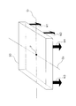
Images


Classifications
-
- H—ELECTRICITY
- H05—ELECTRIC TECHNIQUES NOT OTHERWISE PROVIDED FOR
- H05K—PRINTED CIRCUITS; CASINGS OR CONSTRUCTIONAL DETAILS OF ELECTRIC APPARATUS; MANUFACTURE OF ASSEMBLAGES OF ELECTRICAL COMPONENTS
- H05K1/00—Printed circuits
- H05K1/02—Details
- H05K1/0296—Conductive pattern lay-out details not covered by sub groups H05K1/02 - H05K1/0295
-
- H—ELECTRICITY
- H05—ELECTRIC TECHNIQUES NOT OTHERWISE PROVIDED FOR
- H05K—PRINTED CIRCUITS; CASINGS OR CONSTRUCTIONAL DETAILS OF ELECTRIC APPARATUS; MANUFACTURE OF ASSEMBLAGES OF ELECTRICAL COMPONENTS
- H05K1/00—Printed circuits
- H05K1/02—Details
- H05K1/11—Printed elements for providing electric connections to or between printed circuits
- H05K1/111—Pads for surface mounting, e.g. lay-out
-
- H—ELECTRICITY
- H10—SEMICONDUCTOR DEVICES; ELECTRIC SOLID-STATE DEVICES NOT OTHERWISE PROVIDED FOR
- H10W—GENERIC PACKAGES, INTERCONNECTIONS, CONNECTORS OR OTHER CONSTRUCTIONAL DETAILS OF DEVICES COVERED BY CLASS H10
- H10W70/00—Package substrates; Interposers; Redistribution layers [RDL]
- H10W70/60—Insulating or insulated package substrates; Interposers; Redistribution layers
- H10W70/62—Insulating or insulated package substrates; Interposers; Redistribution layers characterised by their interconnections
- H10W70/65—Shapes or dispositions of interconnections
-
- H—ELECTRICITY
- H10—SEMICONDUCTOR DEVICES; ELECTRIC SOLID-STATE DEVICES NOT OTHERWISE PROVIDED FOR
- H10W—GENERIC PACKAGES, INTERCONNECTIONS, CONNECTORS OR OTHER CONSTRUCTIONAL DETAILS OF DEVICES COVERED BY CLASS H10
- H10W90/00—Package configurations
- H10W90/701—Package configurations characterised by the relative positions of pads or connectors relative to package parts
-
- H—ELECTRICITY
- H05—ELECTRIC TECHNIQUES NOT OTHERWISE PROVIDED FOR
- H05K—PRINTED CIRCUITS; CASINGS OR CONSTRUCTIONAL DETAILS OF ELECTRIC APPARATUS; MANUFACTURE OF ASSEMBLAGES OF ELECTRICAL COMPONENTS
- H05K2201/00—Indexing scheme relating to printed circuits covered by H05K1/00
- H05K2201/09—Shape and layout
- H05K2201/09209—Shape and layout details of conductors
- H05K2201/09654—Shape and layout details of conductors covering at least two types of conductors provided for in H05K2201/09218 - H05K2201/095
- H05K2201/09781—Dummy conductors, i.e. not used for normal transport of current; Dummy electrodes of components
-
- H—ELECTRICITY
- H05—ELECTRIC TECHNIQUES NOT OTHERWISE PROVIDED FOR
- H05K—PRINTED CIRCUITS; CASINGS OR CONSTRUCTIONAL DETAILS OF ELECTRIC APPARATUS; MANUFACTURE OF ASSEMBLAGES OF ELECTRICAL COMPONENTS
- H05K3/00—Apparatus or processes for manufacturing printed circuits
- H05K3/30—Assembling printed circuits with electric components, e.g. with resistors
- H05K3/32—Assembling printed circuits with electric components, e.g. with resistors electrically connecting electric components or wires to printed circuits
- H05K3/34—Assembling printed circuits with electric components, e.g. with resistors electrically connecting electric components or wires to printed circuits by soldering
- H05K3/341—Surface mounted components
- H05K3/3431—Leadless components
- H05K3/3436—Leadless components having an array of bottom contacts, e.g. pad grid array or ball grid array components
-
- H—ELECTRICITY
- H10—SEMICONDUCTOR DEVICES; ELECTRIC SOLID-STATE DEVICES NOT OTHERWISE PROVIDED FOR
- H10W—GENERIC PACKAGES, INTERCONNECTIONS, CONNECTORS OR OTHER CONSTRUCTIONAL DETAILS OF DEVICES COVERED BY CLASS H10
- H10W70/00—Package substrates; Interposers; Redistribution layers [RDL]
- H10W70/60—Insulating or insulated package substrates; Interposers; Redistribution layers
- H10W70/62—Insulating or insulated package substrates; Interposers; Redistribution layers characterised by their interconnections
- H10W70/65—Shapes or dispositions of interconnections
- H10W70/654—Top-view layouts
- H10W70/656—Fan-in layouts
-
- H—ELECTRICITY
- H10—SEMICONDUCTOR DEVICES; ELECTRIC SOLID-STATE DEVICES NOT OTHERWISE PROVIDED FOR
- H10W—GENERIC PACKAGES, INTERCONNECTIONS, CONNECTORS OR OTHER CONSTRUCTIONAL DETAILS OF DEVICES COVERED BY CLASS H10
- H10W74/00—Encapsulations, e.g. protective coatings
-
- H—ELECTRICITY
- H10—SEMICONDUCTOR DEVICES; ELECTRIC SOLID-STATE DEVICES NOT OTHERWISE PROVIDED FOR
- H10W—GENERIC PACKAGES, INTERCONNECTIONS, CONNECTORS OR OTHER CONSTRUCTIONAL DETAILS OF DEVICES COVERED BY CLASS H10
- H10W90/00—Package configurations
- H10W90/701—Package configurations characterised by the relative positions of pads or connectors relative to package parts
- H10W90/751—Package configurations characterised by the relative positions of pads or connectors relative to package parts of bond wires
- H10W90/754—Package configurations characterised by the relative positions of pads or connectors relative to package parts of bond wires between a chip and a stacked insulating package substrate, interposer or RDL
-
- Y—GENERAL TAGGING OF NEW TECHNOLOGICAL DEVELOPMENTS; GENERAL TAGGING OF CROSS-SECTIONAL TECHNOLOGIES SPANNING OVER SEVERAL SECTIONS OF THE IPC; TECHNICAL SUBJECTS COVERED BY FORMER USPC CROSS-REFERENCE ART COLLECTIONS [XRACs] AND DIGESTS
- Y02—TECHNOLOGIES OR APPLICATIONS FOR MITIGATION OR ADAPTATION AGAINST CLIMATE CHANGE
- Y02P—CLIMATE CHANGE MITIGATION TECHNOLOGIES IN THE PRODUCTION OR PROCESSING OF GOODS
- Y02P70/00—Climate change mitigation technologies in the production process for final industrial or consumer products
- Y02P70/50—Manufacturing or production processes characterised by the final manufactured product
Definitions
- the present invention relates to a circuit board including a semiconductor device and a printed board, and a method for manufacturing the circuit board.
- circuit boards including a printed circuit board and a semiconductor device mounted on the printed circuit board are used in electronic devices such as mobile phones, personal computers, and video equipment.
- array packages such as BGA (Ball Grid Array) type and LGA (Land Grid Array) type CSP (Chip size package) are widely known.
- Such a semiconductor device has a plurality of device-side lands that are mechanically connected to a printed circuit board via solder.
- a plurality of device-side lands may be arranged asymmetrically (see, for example, Patent Document 1 and Patent Document 2).
- the present invention has been made to solve the above-described problems, and an object thereof is to provide a circuit board capable of suppressing soldering defects and a method for manufacturing the circuit board.
- a circuit board includes a printed circuit board and a plurality of device-side lands arranged asymmetrically with respect to a predetermined reference point, and a semiconductor device mounted on the printed circuit board. Includes a plurality of device-side connection lands that are mechanically connected to the printed circuit board via solder, and a device-side separation land that is mechanically separated from the printed circuit board.
- circuit board capable of suppressing soldering defects and a method for manufacturing the circuit board.
- FIG. 1 is a plan view of a semiconductor device 20 according to an embodiment. 1 is a plan view of a semiconductor device 20 according to an embodiment. It is sectional drawing in the XX line of FIG. It is a top view of circuit board 100 concerning an embodiment. It is sectional drawing in the YY line
- FIG. 1 is a plan view of the printed circuit board 10 according to the embodiment as viewed from the mounting surface 10S side.
- the printed circuit board 10 includes a substrate body 11 and a plurality of substrate-side lands 12.
- the substrate body 11 is a plate-like member made of paper phenol or glass epoxy.
- the substrate body 11 has a mounting surface 10S.
- On the mounting surface 10S electronic components (for example, a CPU, a resistor, a capacitor, etc.) not shown are mounted.
- the semiconductor device 20 is mounted on the mounting surface 10S.
- the plurality of substrate-side lands 12 are terminals for mounting the semiconductor device 20.
- the plurality of board-side lands 12 are provided on the mounting surface 10S.
- the plurality of substrate-side lands 12 are made of, for example, copper foil.
- the plurality of board-side lands 12 are arranged asymmetrically with respect to a predetermined reference point A in a plan view of the mounting surface 10S. That is, the arrangement of the plurality of substrate-side lands 12 is not point-symmetric.
- the predetermined reference point A is, for example, the center point of the entire plurality of substrate-side lands 12.
- the plurality of substrate-side lands 12 include 45 substrate-side connection lands 12a and four substrate-side separation lands 12b.
- Each board-side connection land 12a is mechanically connected to the semiconductor device 20 via a connection portion 30 (see FIG. 5) described later.
- Each substrate-side separation land 12 b is mechanically separated from the semiconductor device 20.
- the 45 substrate-side connection lands 12 a which are a part of the plurality of substrate-side lands 12 contribute to the bonding of the semiconductor device 20, whereas the four substrate-side separated lands 12 b are formed on the semiconductor device 20. Does not contribute to joining.
- substrate side separation land 12b have the same structure.
- FIG. 2 is a plan view of the semiconductor device 20 according to the embodiment as viewed from the facing surface 20S side.
- FIG. 3 is a plan view of the semiconductor device 20 from which the plurality of solder balls 22 are omitted, as viewed from the facing surface 20S side.
- 4 is a cross-sectional view taken along line XX of FIG. As shown in FIG.
- the semiconductor device 20 includes a package substrate 21 and a plurality of solder balls 22.
- an array package such as BGA (Ball Grid Array) type or LGA (Land Grid Array) type CSP (Chip size package) can be used.
- the package substrate 21 is a plate-like member made of an insulating material.
- the package substrate 21 has a facing surface 20S that faces the mounting surface 10S.
- the plurality of solder balls 22 are spherical members provided on the facing surface 20S.
- the plurality of solder balls 22 are made of solder (for example, an alloy of Sn3Ag0.5Cu (Ag is 3 wt%, Cu is 0.5 wt%, and the rest is Sn)).
- the plurality of solder balls 22 are arranged asymmetrically with reference to an intersection B between the perpendicular surface perpendicular to the opposing surface 20S and passing through the center of gravity of the semiconductor device 20 and the opposing surface 20S.
- the intersection point B passes through the approximate center of the facing surface 20S.
- the plurality of solder balls 22 include 45 connection balls 22a and 4 separation balls 22b.
- Each connection ball 22a mechanically connects the printed circuit board 10 and the semiconductor device 20 by constituting a part of the connection portion 30 (see FIG. 5) when the semiconductor device 20 is mounted. Since each separation ball 22b does not constitute a part of the connection portion 30 when the semiconductor device 20 is mounted, the printed circuit board 10 and the semiconductor device 20 are not mechanically connected.
- the 45 connection balls 22 a which are a part of the plurality of solder balls 22 contribute to the bonding of the semiconductor device 20, whereas the four separation balls 22 b do not contribute to the bonding of the semiconductor device 20.
- each connection ball 22a and each separation ball 22b have the same configuration.
- the semiconductor device 20 has a plurality of device-side lands 23.
- the plurality of device-side lands 23 are arranged asymmetrically with respect to the intersection B.
- the plurality of device-side lands 23 include 42 real lands 23R and seven dummy lands 23D.
- the 42 real lands 23R are mechanically connected to the printed circuit board via the connection portion 30 (see FIG. 5) when the semiconductor device 20 is mounted.
- Each real land 23R is electrically connected to a semiconductor element 24 (see FIG. 4) disposed in the semiconductor device 20. Accordingly, each real land 23 ⁇ / b> R contributes to the function of the semiconductor device 20.
- the 42 real lands 23R include a plurality of signal terminals, a plurality of power supply terminals, a plurality of grounding terminals, and the like.
- the seven dummy lands 23D are electrically separated from the semiconductor element 24 (see FIG. 4). Therefore, each dummy land 23 ⁇ / b> D does not contribute to the function of the semiconductor device 20.
- the seven dummy lands 23D include three first dummy lands 23D 1 and four second dummy lands 23D 2 .
- the first dummy land 23D 1 is mechanically connected to the printed circuit board via the connection portion 30 in the same manner as the 42 real lands 23R.
- the second dummy land 23D 2 is different from the first dummy land 23D 1, mechanically separated from the printed circuit board.
- 42 pieces of real land 23R and the three first dummy land 23D 1 each is connected to each board connection lands 12a.
- 42 pieces of real land 23R and the three first dummy land 23D 1 of constitutes "device-side connection land" to placed 45 corresponding to 45 of the board-side connection lands 12a.
- each second dummy land 23D 2 is disposed at a distance from the four substrate side spaced lands 12b.
- each second dummy land 23D 2 constitutes a “device-side separation land” that does not contribute to the function of the semiconductor device 20 and does not contribute to the bonding between the printed circuit board 10 and the semiconductor device 20.
- the second dummy land 23D 2 is appropriately referred to as “device-side separation land”.
- the semiconductor device 20 includes a semiconductor element 24, a first insertion wiring 25, a second insertion wiring 26, a wire 27, an electrode portion 28, and an exterior body 29.
- the semiconductor element 24 is an active element such as a transistor or an integrated circuit.
- the semiconductor element 24 is electrically connected to the electrode portion 28 of the package substrate 21 through the wire 27.
- One real land 23 ⁇ / b> R is electrically connected to the electrode portion 28 via the first insertion wiring 25.
- Another real land 23 ⁇ / b> R is electrically connected to the electrode portion 28 via the second interpolated wiring 26.
- the semiconductor element 24 is electrically connected to the two real lands 23R.
- the three first dummy lands 23D 1 and the two second dummy lands 23D 2 are electrically separated from the semiconductor element 24.
- FIG. 5 is a plan view of the circuit board 100 according to the embodiment as viewed from the mounting surface 10S side. 6 is a cross-sectional view taken along line YY of FIG. In FIG. 5, the 45 connecting portions 30 are indicated by broken lines, and the four spacing balls 22b are omitted. As shown in FIG. 5, the semiconductor device 20 is mounted on the printed circuit board 10 via 45 connection portions 30.
- connection portions 30 are disposed asymmetrically with respect to a perpendicular C passing through the center of gravity of the semiconductor device 20 and perpendicular to the mounting surface 10S.
- the perpendicular C passes through the intersection B.
- the plurality of device-side lands 23 include a plurality of device-side connection lands that are mechanically connected to the printed circuit board via the connection portion 30.
- seven device side land 23 shown includes five two real land 23R and the three first dummy land 23D 1 of the to be board-side connecting lands 12a and mechanically connected .
- the plurality of device-side lands 23 include device-side separation lands that are mechanically separated from the printed circuit board 10.
- seven device side land 23 shown includes a second dummy land 23D 2 mechanically separated from the two board-side spaced lands 12b.
- connecting portion 30 is mechanically connected to the board-side connecting lands 12a and real land 23R or first dummy land 23D 1.
- the connection portion 30 is formed by fusing the connection balls 22a with the cream solder 40 applied on the board-side connection lands 12a.
- the separation balls 22b maintain the original shape without forming the connection portions 30. Therefore, the separation ball 22b is separated from the substrate-side separation land 12b.
- the interval W between each device-side connection land (each real land 23R and the first dummy land 23D 1 ) and the printed board 10 (each board-side land 12) is uniform.
- the facing surface 20S is substantially parallel to the mounting surface 10S. That is, the semiconductor device 20 is not inclined with respect to the printed circuit board 10.
- cream solder 40 is applied on 45 substrate-side connection lands 12 a that are a part of the plurality of substrate-side lands 12 provided on the printed circuit board 10. At this time, the cream solder 40 is not applied on the four board-side separated lands 12b.
- a plurality of target lands (hereinafter referred to as “a plurality of target lands”) to which the cream solder 40 is to be applied are plural so that the semiconductor device 20 does not tilt with the solidification of the fusion body 30a described later.
- the device-side land 23 is selected.
- the fusion body 30a attempts to rotate the semiconductor device 20.
- the fusion body 30a attempts to rotate the semiconductor device 20.
- only the second dummy land 23D 2 among the plurality of apparatus-side lands 23 are excluded from the plurality of target lands.
- the semiconductor device 20 is placed on the printed circuit board 10 to which the cream solder 40 is applied.
- the lower end portion of each connection ball 22a is in contact with the cream solder 40 applied on each substrate-side connection land 12a.
- the cream solder 40 is not applied to each substrate-side separated land 12b, the lower end portion of each separated ball 22b does not contact the cream solder 40.
- the lower end portion of each separation ball 22b may be in contact with each substrate-side separation land 12b.
- the printed circuit board 10 and the semiconductor device 20 are placed in a heating device such as a reflow furnace, and the solder balls 22 are heated to the melting point or higher.
- the 45 connection balls 22a and the cream solder 40 are fused to form 45 fusion bodies 30a.
- the four spacing balls 22b melt, the cream solder 40 is not applied to the four board-side spacing lands 12b, so that the spacing balls 22b do not fuse with the cream solder 40.
- each fusion body 30a tends to be rounded by surface tension when it is liquefied by melting, and tends to shrink when solidified, so that each device-side connection land is printed by each fusion body 30a. Pulled to the plate 10 side.
- the semiconductor device 20 is subjected to a moment of tensile force by the 45 fusion bodies 30a.
- the cream solder 40 is applied only to a plurality of target lands selected from the plurality of device-side lands 23. Therefore, since the moment applied to the semiconductor device 20 is balanced, the inclination of the semiconductor device 20 is suppressed.
- FIG. 8 is a diagram schematically showing a moment applied to the semiconductor device 20 when the fusion body 30a is melted and solidified. Such a moment is generated according to the moment generated according to the surface tension of the melted fusion body 30a (the force by which the fusion body 30a tries to be small and round) and the contraction force when the fusion body 30a is solidified. Two types of moments are assumed: moments.
- the axis Q 1 passes through the center of gravity P of the semiconductor device 20 and is parallel to the facing surface 20S.
- the axis Q 2 passes through the center of gravity P of the semiconductor device 20, is parallel to the facing surface 20 S, and is perpendicular to the axis Q 1 . As shown in FIG.
- the semiconductor device 20 if a reference axis Q 1, is under the resultant moment M1 and resultant moment M2. Further, when the axis Q 2 is used as a reference, the semiconductor device 20 is applied with the resultant moment M3 and the resultant moment M4.
- the plurality of target lands are selected, for example, so that the combined moment M1 and the combined moment M2 are balanced, and the combined moment M3 and the combined moment M4 are balanced.
- the inclination of the semiconductor device 20 accompanying the melting and solidification of the 45 fusion bodies 30a is suppressed.
- the precision which suppresses the inclination of the semiconductor device 20 improves, so that many reference
- the semiconductor device 20 includes a plurality of device-side lands 23 that are asymmetrically arranged with respect to the intersection B.
- the plurality of device-side lands 23 include 45 device-side connecting lands (42 real lands 23R and three first dummy lands 23D 1 ) and four device-side separated lands (four second dummy lands). 23D 2 ).
- Each device-side connection land is mechanically connected to the printed circuit board 10 via the connection unit 30.
- Each device-side separation land is mechanically separated from the printed circuit board 10.
- the present inventors diligently investigated the cause of the occurrence of cracks in the vicinity of the boundaries between a plurality of device-side lands and solder, and found that the molten solder tried to be rounded by surface tension and the solder solidified. I got the knowledge that it was caused by the force to try to contract when doing. Specifically, for example, if all of the plurality of device-side lands 23 arranged asymmetrically are soldered to the plurality of board-side lands 12, the surface tension of the melted solder and the shrinkage force of the solidified solder are many. It becomes large in the area where the device-side lands 23 are densely packed. As described above, the semiconductor device 20 is inclined with respect to the printed circuit board 10 due to an unbalanced force acting on the semiconductor device 20.
- the circuit board 100 only the first dummy land 23D 1 of the dummy lands 23D is mechanically connected to the printed circuit board 10, and the second dummy land 23D 2 is mechanically connected to the printed circuit board 10. Not connected to. Therefore, compared with the case where all of the dummy lands 23D are mechanically joined to the printed circuit board 10, the surface tension and solidification shrinkage force of the solder are suppressed from being concentrated on a part of the semiconductor device 20. Thereby, since the inclination of the semiconductor device 20 is suppressed, generation
- the intervals between the plurality of device-side lands 23 and the printed circuit board 10 are uniform.
- the height of each of the plurality of connection portions 30 is formed uniformly, for example, the strength of each connection portion 30 is higher than when only a part of the plurality of connection portions 30 is formed elongated. Uniformity can be achieved.
- the facing surface 20S is substantially parallel to the mounting surface 10S.
- the strength of each connection portion 30 can be made uniform.
- the four device-side separation lands (four second dummy lands 23D 2 ) are electrically separated from the semiconductor element 24. As described above, the land that does not originally contribute to the function of the semiconductor device 20 is mechanically separated from the semiconductor device 10. Therefore, the function of the semiconductor device 20 is not deteriorated.
- the method for manufacturing the circuit board 100 includes a step of applying the cream solder 40 onto the 45 substrate-side connection lands 12a that are a part of the plurality of substrate-side lands 12.
- the cream solder 40 is applied only to the 45 substrate-side connection lands 12 a, only 45 device-side connection lands among the plurality of device-side lands 23 are mechanically connected to the printed circuit board 10. Therefore, compared with the case where all of the plurality of device-side lands 23 are mechanically bonded to the printed circuit board 10, it is possible to suppress the concentration of the solder surface tension and solidification contraction force on a part of the semiconductor device 20. As a result, since the semiconductor device 20 can be prevented from tilting, the occurrence of cracks and the like in the connection portion 30 can be reduced.
- the 45 device-side connection lands are arranged asymmetrically with respect to the intersection point B, but may be arranged symmetrically with respect to the intersection point B. In this case, it is possible to balance the moment of force that each device-side connection land is pulled toward the printed circuit board 10 via the connection portion 30 with higher accuracy.
- the four device side spaced lands although the electrically be connected not a four second dummy land 23D 2 in the semiconductor element 24 is not limited thereto.
- the four device-side separated lands may be selected from the real lands 23 ⁇ / b> R electrically connected to the semiconductor element 24.
- the real land 23R as the four device-side separated lands, a part of a plurality of signal terminals, a part of a plurality of power supply terminals, a part of a plurality of grounding terminals for transmitting the same signal repeatedly. It is preferred that some are selected.
- the plurality of device-side lands 23 include 42 real lands 23R, three first dummy lands 23D 1 , and four second dummy lands 23D 2 .
- the number of each land is not limited to this.
- the case where the plurality of device-side lands 23 include one second dummy land 23D 2 is, for example, a plurality of devices arranged in n ⁇ m rows in order to cause the transfer robot to automatically determine the orientation of the semiconductor device 20.
- the transfer robot to automatically determine the orientation of the semiconductor device 20.
- each separation ball 22b is physically (mechanically and electrically) separated from each substrate-side separation land 12b as shown in FIG. is not.
- Each separation ball 22b may be electrically connected to each substrate-side separation land 12b. That is, each separation ball 22b is not mechanically joined to each substrate-side separation land 12b, and is allowed to contact.
- the second dummy land 23D 2 is because it is electrically separated from the semiconductor element 24, there is no effect on the function of the semiconductor device 20.
- the interval W between each device-side connection land and the printed circuit board 10 is uniform. However, the present invention is not limited to this.
- the interval W between each device-side connection land and the printed circuit board 10 may vary within a predetermined range.
- the predetermined range can be set to such an extent that no cracks are generated in the connection portion 30. Further, as long as this is the case, the facing surface 20S may not be completely parallel to the mounting surface 10S.
- the device-side separated land is mechanically separated from the substrate-side separated land 12b by not applying the cream solder 40 to the substrate-side separated land 12b.
- the present invention is not limited to this. Absent.
- the apparatus-side separation land can be mechanically separated from the substrate-side separation land 12b by not providing the separation balls 22b on the apparatus-side separation land.
- the present invention naturally includes various embodiments not described herein. Therefore, the technical scope of the present invention is defined only by the invention specifying matters according to the scope of claims reasonable from the above description.
- circuit board capable of suppressing soldering defects and a manufacturing method thereof, which is useful in the field of electronic equipment.
Landscapes
- Engineering & Computer Science (AREA)
- Microelectronics & Electronic Packaging (AREA)
- Electric Connection Of Electric Components To Printed Circuits (AREA)
- Wire Bonding (AREA)
- Semiconductor Integrated Circuits (AREA)
- Design And Manufacture Of Integrated Circuits (AREA)
- Physics & Mathematics (AREA)
- Geometry (AREA)
Abstract
Description
ここで、搬送ロボットに半導体装置の向きを自動判別させるために、複数の装置側ランドが非対称に配置される場合がある(例えば、特許文献1及び特許文献2参照)。
本発明は、上述の課題を解決するためになされたものであり、半田付け不良を抑制可能な回路基板、及びその製造方法を提供することを目的とする。
(概要)
本実施形態では、半導体装置をプリント基板に半田付けする際、所定の軸を基準として半導体装置にかかる力のモーメントを釣り合わせることによって、半導体装置のプリント基板に対する傾きを抑制するものである。
以下、プリント基板、半導体装置、及び回路基板の構成、及び回路基板の製造方法について順に説明する。
実施形態に係るプリント基板の構成について、図面を参照しながら説明する。図1は、実施形態に係るプリント基板10を実装面10S側から見た平面図である。
図1に示すように、プリント基板10は、基板本体11と複数の基板側ランド12とを有する。
基板本体11は、紙フェノールやガラスエポキシなどによって構成される板状部材である。基板本体11は、実装面10Sを有する。実装面10Sには、図示しない電子部品(例えば、CPU、抵抗器、コンデンサーなど)が実装される。本実施形態では、後述するように、半導体装置20が実装面10Sに実装される。
複数の基板側ランド12は、半導体装置20を実装するための端子である。複数の基板側ランド12は、実装面10S上に設けられる。複数の基板側ランド12は、例えば、銅箔などによって構成される。
本実施形態において、複数の基板側ランド12は、45個の基板側接続ランド12aと、4個の基板側離間ランド12bと、を含む。各基板側接続ランド12aは、後述する接続部30(図5参照)を介して、半導体装置20と機械的に接続される。各基板側離間ランド12bは、半導体装置20から機械的に離間する。このように、複数の基板側ランド12の一部である45個の基板側接続ランド12aが半導体装置20の接合に寄与するのに対して、4個の基板側離間ランド12bは半導体装置20の接合に寄与しない。ただし、各基板側接続ランド12aと各基板側離間ランド12bとは、同一の構成を有している。
(半導体装置の構成)
実施形態に係る半導体装置の構成について、図面を参照しながら説明する。図2は、実施形態に係る半導体装置20を対向面20S側から見た平面図である。図3は、複数の半田ボール22が省略された半導体装置20を対向面20S側から見た平面図である。図4は、図2のX-X線における断面図である。
図2に示すように、半導体装置20は、パッケージ基板21と、複数の半田ボール22と、を有する。半導体装置20としては、BGA(Ball Grid Array)型やLGA(Land Grid Array)型のCSP(Chip size package)のようなアレイパッケージを用いることができる。
複数の半田ボール22は、対向面20S上に設けられる球状部材である。複数の半田ボール22は、半田(例えば、Sn3Ag0.5Cu(Agが3wt%、Cuが0.5wt%、残りがSn)の合金)によって構成される。複数の半田ボール22は、対向面20Sに垂直かつ半導体装置20の重心を通る垂線と対向面20Sとの交点Bを基準として、非対称に配置されている。なお、本実施形態では、交点Bは、対向面20Sの略中心を通る。
複数の半田ボール22は、45個の接続ボール22aと4個の離間ボール22bとを含む。各接続ボール22aは、半導体装置20を実装する際、接続部30(図5参照)の一部を構成することによって、プリント基板10と半導体装置20とを機械的に接続する。各離間ボール22bは、半導体装置20を実装する際、接続部30の一部を構成しないので、プリント基板10と半導体装置20とを機械的に接続しない。このように、複数の半田ボール22の一部である45個の接続ボール22aが半導体装置20の接合に寄与するのに対して、4個の離間ボール22bは半導体装置20の接合に寄与しない。ただし、各接続ボール22aと各離間ボール22bとは、同一の構成を有している。
本実施形態において、複数の装置側ランド23は、42個のリアルランド23Rと、7個のダミーランド23Dとを含む。
42個のリアルランド23Rは、半導体装置20を実装する際、接続部30(図5参照)を介して、プリント基板と機械的に接続される。各リアルランド23Rは、半導体装置20内に配置される半導体素子24(図4参照)と電気的に接続されている。従って、各リアルランド23Rは、半導体装置20の機能に寄与している。42個のリアルランド23Rには、複数の信号端子、複数の電源端子、複数の接地用端子などが含まれている。
7個のダミーランド23Dは、半導体素子24から電気的に離間している(図4参照)。従って、各ダミーランド23Dは、半導体装置20の機能には寄与しない。
本実施形態において、42個のリアルランド23R及び3個の第1ダミーランド23D1それぞれは、各基板側接続ランド12aと接続される。このように、42個のリアルランド23R及び3個の第1ダミーランド23D1は、45個の基板側接続ランド12aに対応して配置された45個の「装置側接続ランド」を構成する。以下の説明では、適宜、リアルランド23Rと第1ダミーランド23D1とを合わせて「装置側接続ランド」と併称する。なお、45個の装置側接続ランドは、図3に示すように、交点Bを基準として、非対称に配置されている。
図4に示すように、半導体装置20は、半導体素子24と、第1内挿配線25と、第2内挿配線26と、ワイヤー27と、電極部28と、外装体29とを有する。
半導体素子24は、トランジスタや集積回路などの能動素子である。半導体素子24は、ワイヤー27を介して、パッケージ基板21の電極部28と電気的に接続されている。一つのリアルランド23Rは、第1内挿配線25を介して、電極部28と電気的に接続される。もう一つのリアルランド23Rは、第2内挿配線26を介して、電極部28と電気的に接続される。これにより、半導体素子24は、2個のリアルランド23Rと電気的に接続されている。一方で、3個の第1ダミーランド23D1と2個の第2ダミーランド23D2とは、半導体素子24から電気的に離間されている。
(回路基板の構成)
実施形態に係る回路基板の構成について、図面を参照しながら説明する。図5は、実施形態に係る回路基板100を実装面10S側から見た平面図である。図6は、図5のY-Y線における断面図である。なお、図5では、45個の接続部30を破線で示し、4個の離間ボール22bを省略している。
図5に示すように、半導体装置20は、45個の接続部30を介して、プリント基板10に実装される。本実施形態において、45個の接続部30は、半導体装置20の重心を通り、実装面10Sに垂直な垂線Cを基準として、非対称に配置されている。なお、本実施形態において、垂線Cは交点Bを通る。
また、複数の装置側ランド23は、プリント基板10から機械的に離間する装置側離間ランドを含む。具体的に、図示された7個の装置側ランド23は、2個の基板側離間ランド12bから機械的に離間する第2ダミーランド23D2を含む。
このように、接続部30は、基板側接続ランド12aとリアルランド23R又は第1ダミーランド23D1とを機械的に接続する。接続部30は、後述するように、接続ボール22aが基板側接続ランド12a上に塗布されたクリーム半田40と融合することによって、形成される。
本実施形態において、各装置側接続ランド(各リアルランド23R及び第1ダミーランド23D1)とプリント基板10(各基板側ランド12)との間隔Wは、均一である。また、本実施形態において、対向面20Sは、実装面10Sに略平行である。すなわち、半導体装置20は、プリント基板10に対して傾いていない。
(回路基板の製造方法)
実施形態に係る回路基板の製造方法について、図面を参照しながら説明する。図7A~図7Cは、実施形態に係る回路基板100の製造方法を説明するための断面図である。
ここで、クリーム半田40を塗布する対象となる複数の対象ランド(以下、「複数の対象ランド」という。)は、後述する融合体30aの固化に伴って半導体装置20が傾かないように、複数の装置側ランド23の中から選択される。
具体的に、複数の対象ランドは、半導体装置20の重心を通り、かつ、対向面20Sに平行な複数の軸を基準とした場合に、融合体30aが半導体装置20を回転させようとするモーメントが釣り合うように選択される(図8参照)。本実施形態において、複数の装置側ランド23のうち第2ダミーランド23D2だけが、複数の対象ランドから除外されている。
次に、図7Cに示すように、リフロー炉などの加熱装置にプリント基板10及び半導体装置20を入れて、半田ボール22を融点以上に加熱する。この際、45個の接続ボール22aとクリーム半田40とが融合して、45個の融合体30aが形成される。一方で、4個の離間ボール22bは溶融するものの、4個の基板側離間ランド12bにクリーム半田40が塗布されていないので、各離間ボール22bは各クリーム半田40と融合しない。
ここで、各融合体30aは、溶融により液化した際に表面張力によって小さく丸まろうとし、また、固化する際に収縮しようとするため、各装置側接続ランドは、各融合体30aによってプリント配線板10側に引っ張られる。そのため、半導体装置20には、45個の融合体30aによる引っ張り力のモーメントがかかる。
本実施形態では、上述の通り、複数の装置側ランド23の中から選択された複数の対象ランドにのみクリーム半田40が塗布されている。そのため、半導体装置20にかかるモーメントが釣り合うので、半導体装置20の傾きは抑制される。
図8において、軸線Q1は、半導体装置20の重心Pを通り、対向面20Sに平行である。軸線Q2は、半導体装置20の重心Pを通り、対向面20Sに平行であって、かつ、軸線Q1に垂直である。
図8に示すように、半導体装置20には、軸線Q1を基準とすれば、合モーメントM1と合モーメントM2とがかかっている。また、半導体装置20には、軸線Q2を基準とすれば、合モーメントM3と合モーメントM4とがかかっている。複数の対象ランドは、例えば、合モーメントM1と合モーメントM2とが釣り合い、かつ、合モーメントM3と合モーメントM4とが釣り合うように選択される。その結果、45個の融合体30aの溶融及び固化に伴う半導体装置20の傾きが抑制される。なお、基準とする軸線を多く設定するほど、半導体装置20の傾きを抑制する精度は向上する。
(1)本実施形態に係る回路基板100において、半導体装置20は、交点Bを基準として非対称に配置される複数の装置側ランド23を有する。複数の装置側ランド23は、45個の装置側接続ランド(42個のリアルランド23R及び3個の第1ダミーランド23D1)と、4個の装置側離間ランド(4個の第2ダミーランド23D2)とを含む。各装置側接続ランドは、接続部30を介して、プリント基板10と機械的に接続される。各装置側離間ランドは、プリント基板10から機械的に離間する。
ここで、本発明者らが、複数の装置側ランドと半田との境界付近にクラックが発生する原因について鋭意検討したところ、溶融した半田が表面張力によって小さく丸まろうとする力と、半田が固化する際に収縮しようとする力とに起因するという知見を得た。具体的には、例えば、非対称に配置された複数の装置側ランド23の全てを複数の基板側ランド12に半田付けすれば、溶融した半田の表面張力や固化する半田の収縮力は、多くの装置側ランド23が密集する領域で大きくなる。このように、半導体装置20に不均衡な力が働くことによって、半導体装置20は、プリント基板10に対して傾いてしまう。
(2)本実施形態に係る回路基板100において、複数の装置側ランド23それぞれとプリント基板10との間隔は、均一である。
このように、複数の接続部30それぞれの高さが均一に形成されているため、例えば、複数の接続部30の一部だけが細長く形成される場合に比べて、各接続部30の強度の均一化を図ることができる。
(4)本実施形態に係る回路基板100において、4個の装置側離間ランド(4個の第2ダミーランド23D2)は、半導体素子24から電気的に離間している。
このように、もともと半導体装置20の機能に寄与しないランドが半導体装置10から機械的に離間されている。そのため、半導体装置20の機能を低下させることがない。
(5)本実施形態に係る回路基板100の製造方法は、複数の基板側ランド12の一部である45個の基板側接続ランド12a上にクリーム半田40を塗布する工程を備える。
このように、45個の基板側接続ランド12aだけにクリーム半田40を塗布するので、複数の装置側ランド23のうち45個の装置側接続ランドだけがプリント基板10と機械的に接続される。従って、複数の装置側ランド23の全部がプリント基板10と機械的に接合される場合に比べて、半田の表面張力及び固化収縮力が半導体装置20の一部に集中することを抑制できる。その結果、半導体装置20が傾くことを抑制できるので、接続部30におけるクラックなどの発生を低減できる。
従って、半導体装置20がプリント基板10に対して傾くことを精度良く抑制できるので、半田付け不良をより抑制することができる。
(その他の実施形態)
本発明は上記の実施形態によって記載したが、この開示の一部をなす論述及び図面はこの発明を限定するものであると理解すべきではない。この開示から当業者には様々な代替実施形態、実施例及び運用技術が明らかとなろう。
(A)上記実施形態において、45個の装置側接続ランドは、交点Bを基準として非対称に配置されることとしたが、交点Bを基準として対称に配置されていてもよい。この場合には、各装置側接続ランドが接続部30を介してプリント基板10側に引っ張られる力のモーメントを、より精度良く釣り合わせることができる。
(C)上記実施形態において、複数の装置側ランド23は、42個のリアルランド23R、3個の第1ダミーランド23D1、及び4個の第2ダミーランド23D2を含むこととしたが、各ランドの個数はこれに限られるものではない。複数の装置側ランド23は、2個以上のリアルランド23Rと、1つ以上の第2ダミーランド23D2とを含んでいればよく、第1ダミーランド23D1を含んでいなくてもよい。なお、複数の装置側ランド23が1個の第2ダミーランド23D2を含む場合とは、例えば、搬送ロボットに半導体装置20の向きを自動判別させるために、n×m列に整列された複数の装置側ランド23のうち1つだけが欠けている場合等が挙げられる。
(E)上記実施形態において、各装置側接続ランドとプリント基板10との間隔Wは、均一であることとしたが、これに限られるものではない。各装置側接続ランドとプリント基板10との間隔Wは、所定の範囲内でばらついていてもよい。所定の範囲とは、接続部30にクラックが発生しない程度に設定することができる。また、この限りにおいて、対向面20Sは、実装面10Sと完全には平行でなくてもよい。
このように、本発明はここでは記載していない様々な実施形態等を含むことは勿論である。従って、本発明の技術的範囲は上記の説明から妥当な特許請求の範囲に係る発明特定事項によってのみ定められるものである。
10S…実装面
11…基板本体
12…複数の基板側ランド
12a…基板側接続ランド
12b…基板側離間ランド
20…半導体装置
20S…対向面
21…パッケージ基板
22…複数の半田ボール
22a…接続ボール
22b…離間ボール
23…複数の装置側ランド
23R…リアルランド
23D…ダミーランド
23D1…第1ダミーランド
23D2…第2ダミーランド
23…半導体素子
23…複数の装置側ランド
24…半導体素子
25…第1内挿配線
26…第2内挿配線
27…ワイヤー
28…電極部
29…外装体
30…接続部
30a…融合体
40…クリーム半田
A、B…交点
C…垂線
Claims (11)
- プリント基板と、
前記複数の装置側ランドは、半田を介して前記プリント基板と機械的に接続される複数の装置側接続ランドと、前記プリント基板から機械的に離間する装置側離間ランドとを含み、所定の基準点を基準として非対称に配置される複数の装置側ランドを有し、前記プリント基板に実装される半導体装置と、
を備える回路基板。 - 前記半導体装置は、前記装置側離間ランドに接続され、前記プリント基板とは機械的に離間する半田ボールを有する、
請求項1に記載の回路基板。 - 前記半導体装置は、半導体素子を有しており、
前記装置側離間ランドは、前記半導体素子から電気的に離間するダミーランドである、
請求項1又は2に記載の回路基板。 - 前記複数の装置側ランドそれぞれと前記プリント基板との間隔は、略均一である、
請求項1乃至3のいずれかに記載の回路基板。 - 前記プリント基板は、前記半導体装置が実装される実装面を有し、
前記半導体装置は、前記プリント実装面と対向する対向面を有しており、
前記対向面は、前記実装面と略平行である、
請求項1乃至4のいずれかに記載の回路基板。 - 前記複数の装置側接続ランドは、前記所定の基準点を基準とする点対称に配置されている、
請求項1乃至5のいずれかに記載の回路基板。 - 前記半導体装置は、半導体素子を有しており、
前記複数の装置側接続ランドは、前記半導体素子に電気的に接続されるリアルランドと、前記半導体素子から電気的に離間するダミーランドと、を含み、
前記装置側離間ランドは、前記半導体素子から電気的に離間している、
請求項1乃至6のいずれかに記載の回路基板。 - 前記複数の装置側接続ランドは、前記半導体素子に電気的に接続されるリアルランドと、前記半導体素子から電気的に離間するダミーランドと、を含み、
前記装置側離間ランドは、前記半導体素子に電気的に接続されている、
請求項1乃至6のいずれかに記載の回路基板。 - プリント基板に設けられ、所定の基準点を基準として非対称に配置される複数の基板側ランドの一部である複数の基板側接続ランド上にクリーム半田を塗布する塗布工程と、
半導体装置に設けられ、前記複数の基板側ランドに対応する複数の装置側ランド上に形成される半田ボールと、前記複数の基板側接続ランド上に塗布された前記クリーム半田とを融合固化することによって、前記複数の基板側接続ランドを前記複数の装置側ランドの一部に接合する接合工程と、
を備える回路基板の製造方法。 - 前記塗布工程において、
前記複数の基板側ランドのうち前記複数の基板側接続ランドとは異なる基板側ランド上には、クリーム半田を塗布しない、
請求項9に記載の回路基板の製造方法。 - 前記接合工程において、
前記半田ボールが溶融及び固化収縮する際、前記半導体装置の重心を通り、前記半導体装置が有する前記プリント基板と対向する対向面に平行な軸線を基準として、前記複数の装置側ランドそれぞれが前記半田によって前記プリント基板側に引っ張られる力のモーメントを釣り合わせる、
請求項9又は10に記載の回路基板の製造方法。
Priority Applications (3)
| Application Number | Priority Date | Filing Date | Title |
|---|---|---|---|
| JP2012527480A JP5870303B2 (ja) | 2010-08-06 | 2010-12-20 | 回路基板及びその製造方法 |
| US13/809,186 US9198284B2 (en) | 2010-08-06 | 2010-12-20 | Circuit board and method for manufacturing same |
| CN201080067544.XA CN102959699B (zh) | 2010-08-06 | 2010-12-20 | 电路基板及其制造方法 |
Applications Claiming Priority (2)
| Application Number | Priority Date | Filing Date | Title |
|---|---|---|---|
| JP2010-176990 | 2010-08-06 | ||
| JP2010176990 | 2010-08-06 |
Publications (1)
| Publication Number | Publication Date |
|---|---|
| WO2012017507A1 true WO2012017507A1 (ja) | 2012-02-09 |
Family
ID=45559039
Family Applications (1)
| Application Number | Title | Priority Date | Filing Date |
|---|---|---|---|
| PCT/JP2010/007354 Ceased WO2012017507A1 (ja) | 2010-08-06 | 2010-12-20 | 回路基板及びその製造方法 |
Country Status (4)
| Country | Link |
|---|---|
| US (1) | US9198284B2 (ja) |
| JP (1) | JP5870303B2 (ja) |
| CN (1) | CN102959699B (ja) |
| WO (1) | WO2012017507A1 (ja) |
Cited By (2)
| Publication number | Priority date | Publication date | Assignee | Title |
|---|---|---|---|---|
| JP2016502262A (ja) * | 2012-12-21 | 2016-01-21 | ▲華▼▲為▼終端有限公司Huawei Device Co., Ltd. | 電子装置及びランド・グリッド・アレイモジュール |
| US20230067845A1 (en) * | 2021-08-30 | 2023-03-02 | International Business Machines Corporation | Creating a standoff for a low-profile component without adding a process step |
Families Citing this family (8)
| Publication number | Priority date | Publication date | Assignee | Title |
|---|---|---|---|---|
| US9171798B2 (en) * | 2013-01-25 | 2015-10-27 | Taiwan Semiconductor Manufacturing Company, Ltd. | Methods and apparatus for transmission lines in packages |
| ES2565548B1 (es) * | 2014-09-03 | 2017-01-25 | Ontech Security, Sl | Sensor de campos electrostáticos y sistema de seguridad en ambientes industriales |
| KR102339899B1 (ko) * | 2014-12-12 | 2021-12-15 | 삼성전자주식회사 | 반도체 패키지, 모듈 기판 및 이를 포함하는 반도체 패키지 모듈 |
| KR102377472B1 (ko) * | 2015-03-10 | 2022-03-23 | 삼성전자주식회사 | 반도체 패키지 및 그 제조방법 |
| WO2019024058A1 (zh) * | 2017-08-03 | 2019-02-07 | 华为技术有限公司 | 一种栅格阵列封装模块及终端 |
| CN108711272A (zh) * | 2018-05-28 | 2018-10-26 | 上海理工大学 | 一种基于NB-IoT的物体倾覆预警系统 |
| KR102785620B1 (ko) | 2020-06-15 | 2025-03-26 | 삼성전자주식회사 | 인쇄 회로 기판을 포함하는 전자 장치 |
| CN116056321B (zh) * | 2022-08-05 | 2023-10-20 | 荣耀终端有限公司 | 电路板、电路板组件和电子设备 |
Citations (4)
| Publication number | Priority date | Publication date | Assignee | Title |
|---|---|---|---|---|
| JP2003110055A (ja) * | 2001-09-28 | 2003-04-11 | Mitsumi Electric Co Ltd | 表面実装型半導体パッケージ |
| JP2004063761A (ja) * | 2002-07-29 | 2004-02-26 | Nec Electronics Corp | 半導体装置 |
| JP2005108996A (ja) * | 2003-09-29 | 2005-04-21 | Seiko Epson Corp | パッケージic、実装構造体、実装構造体を搭載した電気光学装置、および電気光学装置を搭載した電子機器 |
| JP2008172060A (ja) * | 2007-01-12 | 2008-07-24 | Oki Electric Ind Co Ltd | 半導体装置及びその製造方法 |
Family Cites Families (36)
| Publication number | Priority date | Publication date | Assignee | Title |
|---|---|---|---|---|
| US3458925A (en) * | 1966-01-20 | 1969-08-05 | Ibm | Method of forming solder mounds on substrates |
| US3871014A (en) * | 1969-08-14 | 1975-03-11 | Ibm | Flip chip module with non-uniform solder wettable areas on the substrate |
| US5157480A (en) * | 1991-02-06 | 1992-10-20 | Motorola, Inc. | Semiconductor device having dual electrical contact sites |
| US5186383A (en) * | 1991-10-02 | 1993-02-16 | Motorola, Inc. | Method for forming solder bump interconnections to a solder-plated circuit trace |
| US5269453A (en) * | 1992-04-02 | 1993-12-14 | Motorola, Inc. | Low temperature method for forming solder bump interconnections to a plated circuit trace |
| US5465152A (en) * | 1994-06-03 | 1995-11-07 | Robotic Vision Systems, Inc. | Method for coplanarity inspection of package or substrate warpage for ball grid arrays, column arrays, and similar structures |
| TW303427B (ja) * | 1994-06-10 | 1997-04-21 | Sony Co Ltd | |
| JP3310499B2 (ja) * | 1995-08-01 | 2002-08-05 | 富士通株式会社 | 半導体装置 |
| US5726502A (en) * | 1996-04-26 | 1998-03-10 | Motorola, Inc. | Bumped semiconductor device with alignment features and method for making the same |
| JPH09306954A (ja) * | 1996-05-20 | 1997-11-28 | Hitachi Ltd | 半導体装置及びその実装方法並びに実装構造体 |
| US5859474A (en) * | 1997-04-23 | 1999-01-12 | Lsi Logic Corporation | Reflow ball grid array assembly |
| JPH1174407A (ja) * | 1997-08-29 | 1999-03-16 | Mitsubishi Electric Corp | 半導体装置 |
| JPH11132737A (ja) | 1997-10-29 | 1999-05-21 | Juki Corp | 画像処理方法 |
| GB2344550A (en) * | 1998-12-09 | 2000-06-14 | Ibm | Pad design for electronic package |
| JP3437107B2 (ja) | 1999-01-27 | 2003-08-18 | シャープ株式会社 | 樹脂封止型半導体装置 |
| US6222277B1 (en) * | 1999-06-23 | 2001-04-24 | Emc Corporation | Non-collapsing interconnection for semiconductor devices |
| US6781245B2 (en) * | 2001-01-08 | 2004-08-24 | Siliconware Precision Industries Co., Ltd. | Array structure of solder balls able to control collapse |
| JP2003100801A (ja) | 2001-09-25 | 2003-04-04 | Mitsubishi Electric Corp | 半導体装置 |
| JP3978369B2 (ja) * | 2002-05-20 | 2007-09-19 | アルプス電気株式会社 | 高周波モジュールの取付構造 |
| CN100472770C (zh) * | 2003-01-30 | 2009-03-25 | 高通股份有限公司 | 具有未电连接的焊锡球的区域阵列封装件 |
| US6762495B1 (en) | 2003-01-30 | 2004-07-13 | Qualcomm Incorporated | Area array package with non-electrically connected solder balls |
| DE10341206A1 (de) * | 2003-09-04 | 2005-04-14 | Infineon Technologies Ag | Anordnung zur Verbesserung der Zuverlässigkeit von BGA-Lötverbindungen |
| JP2005166794A (ja) * | 2003-12-01 | 2005-06-23 | Ricoh Co Ltd | 部品パッケージとプリント配線基板および電子機器 |
| US7109583B2 (en) * | 2004-05-06 | 2006-09-19 | Endwave Corporation | Mounting with auxiliary bumps |
| JP4401253B2 (ja) | 2004-06-30 | 2010-01-20 | Necエレクトロニクス株式会社 | 電子部品用パッケージ及びそれを用いた半導体装置 |
| JP2006222374A (ja) * | 2005-02-14 | 2006-08-24 | Fuji Film Microdevices Co Ltd | 半導体チップ |
| JP2006294670A (ja) | 2005-04-06 | 2006-10-26 | Renesas Technology Corp | 半導体装置の製造方法 |
| KR100702969B1 (ko) * | 2005-04-19 | 2007-04-03 | 삼성전자주식회사 | 더미 솔더 볼을 갖는 bga형 반도체 칩 패키지의 기판 실장 구조 |
| JP2006344824A (ja) | 2005-06-09 | 2006-12-21 | Nec Electronics Corp | 半導体装置および半導体装置の製造方法 |
| TWI366902B (en) * | 2007-02-16 | 2012-06-21 | Taiwan Tft Lcd Ass | Bump structure on a substrate |
| JP4424449B2 (ja) | 2007-05-02 | 2010-03-03 | 株式会社村田製作所 | 部品内蔵モジュール及びその製造方法 |
| US7855397B2 (en) * | 2007-09-14 | 2010-12-21 | Nextreme Thermal Solutions, Inc. | Electronic assemblies providing active side heat pumping |
| US8525333B2 (en) | 2008-03-17 | 2013-09-03 | Renesas Electronics Corporation | Electronic device and manufacturing method therefor |
| US7989959B1 (en) * | 2009-01-29 | 2011-08-02 | Xilinx, Inc. | Method of forming stacked-die integrated circuit |
| US8093708B2 (en) * | 2009-07-06 | 2012-01-10 | Sony Ericsson Mobile Communications Ab | Semiconductor package having non-uniform contact arrangement |
| KR20130010359A (ko) * | 2011-07-18 | 2013-01-28 | 삼성전자주식회사 | 반도체 장치용 기판 및 그를 포함한 반도체 장치 |
-
2010
- 2010-12-20 JP JP2012527480A patent/JP5870303B2/ja not_active Expired - Fee Related
- 2010-12-20 US US13/809,186 patent/US9198284B2/en not_active Expired - Fee Related
- 2010-12-20 WO PCT/JP2010/007354 patent/WO2012017507A1/ja not_active Ceased
- 2010-12-20 CN CN201080067544.XA patent/CN102959699B/zh not_active Expired - Fee Related
Patent Citations (4)
| Publication number | Priority date | Publication date | Assignee | Title |
|---|---|---|---|---|
| JP2003110055A (ja) * | 2001-09-28 | 2003-04-11 | Mitsumi Electric Co Ltd | 表面実装型半導体パッケージ |
| JP2004063761A (ja) * | 2002-07-29 | 2004-02-26 | Nec Electronics Corp | 半導体装置 |
| JP2005108996A (ja) * | 2003-09-29 | 2005-04-21 | Seiko Epson Corp | パッケージic、実装構造体、実装構造体を搭載した電気光学装置、および電気光学装置を搭載した電子機器 |
| JP2008172060A (ja) * | 2007-01-12 | 2008-07-24 | Oki Electric Ind Co Ltd | 半導体装置及びその製造方法 |
Cited By (4)
| Publication number | Priority date | Publication date | Assignee | Title |
|---|---|---|---|---|
| JP2016502262A (ja) * | 2012-12-21 | 2016-01-21 | ▲華▼▲為▼終端有限公司Huawei Device Co., Ltd. | 電子装置及びランド・グリッド・アレイモジュール |
| US9905918B2 (en) | 2012-12-21 | 2018-02-27 | Huawei Device Co., Ltd. | Electronic apparatus and land grid array module |
| US20230067845A1 (en) * | 2021-08-30 | 2023-03-02 | International Business Machines Corporation | Creating a standoff for a low-profile component without adding a process step |
| US11812562B2 (en) * | 2021-08-30 | 2023-11-07 | International Business Machines Corporation | Creating a standoff for a low-profile component without adding a process step |
Also Published As
| Publication number | Publication date |
|---|---|
| JP5870303B2 (ja) | 2016-02-24 |
| CN102959699A (zh) | 2013-03-06 |
| US9198284B2 (en) | 2015-11-24 |
| JPWO2012017507A1 (ja) | 2013-09-19 |
| US20130107484A1 (en) | 2013-05-02 |
| CN102959699B (zh) | 2015-12-09 |
Similar Documents
| Publication | Publication Date | Title |
|---|---|---|
| JP5870303B2 (ja) | 回路基板及びその製造方法 | |
| US8368195B2 (en) | Semiconductor device including arrangement to control connection height and alignment between a plurity of stacked semiconductor chips | |
| US8120166B2 (en) | Semiconductor package and method of manufacturing the same, and semiconductor device and method of manufacturing the same | |
| JP3069792B2 (ja) | チップサイズ半導体パッケ―ジ及びその集合体並びにその製造方法 | |
| CN101897175B (zh) | 焊接连接可靠性改进的可回焊相机模块 | |
| US10177131B2 (en) | Semiconductor packages and methods of manufacturing the same | |
| CN103367302A (zh) | 基板装置 | |
| JP5881829B2 (ja) | クワッドフラットノーリードパッケージ体をパッケージングする方法、及びパッケージ体 | |
| CN101145551A (zh) | 集成器件 | |
| KR101519458B1 (ko) | 핀 부착 | |
| JP2011171427A (ja) | 積層型半導体装置 | |
| JP4965989B2 (ja) | 電子部品内蔵基板および電子部品内蔵基板の製造方法 | |
| WO2011125434A1 (ja) | 電子装置 | |
| JP2005123463A (ja) | 半導体装置及びその製造方法、半導体装置モジュール、回路基板並びに電子機器 | |
| JP5672769B2 (ja) | 半導体装置及びその製造方法 | |
| KR101111426B1 (ko) | 코팅된 솔더볼을 갖는 반도체 장치 | |
| JP5342359B2 (ja) | 撮像モジュール及び撮像装置、並びに撮像モジュールの製造方法 | |
| JP5934057B2 (ja) | プリント回路基板 | |
| JP4606376B2 (ja) | 半導体装置 | |
| JP2011258709A (ja) | 相互接続構造、及び相互接続方法 | |
| JP2023087886A (ja) | 電子モジュール、電子機器、中間接続ユニット、中間接続ユニットの製造方法、及び電子モジュールの製造方法 | |
| JP3604001B2 (ja) | 半導体装置の製造方法 | |
| KR20120059796A (ko) | 스프링을 이용한 적층 패키지 및 그 제조방법 | |
| KR20120032762A (ko) | 플립칩 패키지 및 이의 제조 방법 | |
| JP2022003676A (ja) | 電子制御装置および電子制御装置の製造方法 |
Legal Events
| Date | Code | Title | Description |
|---|---|---|---|
| WWE | Wipo information: entry into national phase |
Ref document number: 201080067544.X Country of ref document: CN |
|
| 121 | Ep: the epo has been informed by wipo that ep was designated in this application |
Ref document number: 10855597 Country of ref document: EP Kind code of ref document: A1 |
|
| WWE | Wipo information: entry into national phase |
Ref document number: 2012527480 Country of ref document: JP |
|
| WWE | Wipo information: entry into national phase |
Ref document number: 13809186 Country of ref document: US |
|
| NENP | Non-entry into the national phase |
Ref country code: DE |
|
| 122 | Ep: pct application non-entry in european phase |
Ref document number: 10855597 Country of ref document: EP Kind code of ref document: A1 |