WO2012020771A1 - 積層体および積層体の製造方法 - Google Patents
積層体および積層体の製造方法 Download PDFInfo
- Publication number
- WO2012020771A1 WO2012020771A1 PCT/JP2011/068191 JP2011068191W WO2012020771A1 WO 2012020771 A1 WO2012020771 A1 WO 2012020771A1 JP 2011068191 W JP2011068191 W JP 2011068191W WO 2012020771 A1 WO2012020771 A1 WO 2012020771A1
- Authority
- WO
- WIPO (PCT)
- Prior art keywords
- gas barrier
- barrier layer
- gas
- laminate
- film
- Prior art date
- Legal status (The legal status is an assumption and is not a legal conclusion. Google has not performed a legal analysis and makes no representation as to the accuracy of the status listed.)
- Ceased
Links
Images


Classifications
-
- C—CHEMISTRY; METALLURGY
- C23—COATING METALLIC MATERIAL; COATING MATERIAL WITH METALLIC MATERIAL; CHEMICAL SURFACE TREATMENT; DIFFUSION TREATMENT OF METALLIC MATERIAL; COATING BY VACUUM EVAPORATION, BY SPUTTERING, BY ION IMPLANTATION OR BY CHEMICAL VAPOUR DEPOSITION, IN GENERAL; INHIBITING CORROSION OF METALLIC MATERIAL OR INCRUSTATION IN GENERAL
- C23C—COATING METALLIC MATERIAL; COATING MATERIAL WITH METALLIC MATERIAL; SURFACE TREATMENT OF METALLIC MATERIAL BY DIFFUSION INTO THE SURFACE, BY CHEMICAL CONVERSION OR SUBSTITUTION; COATING BY VACUUM EVAPORATION, BY SPUTTERING, BY ION IMPLANTATION OR BY CHEMICAL VAPOUR DEPOSITION, IN GENERAL
- C23C16/00—Chemical coating by decomposition of gaseous compounds, without leaving reaction products of surface material in the coating, i.e. chemical vapour deposition [CVD] processes
- C23C16/44—Chemical coating by decomposition of gaseous compounds, without leaving reaction products of surface material in the coating, i.e. chemical vapour deposition [CVD] processes characterised by the method of coating
-
- C—CHEMISTRY; METALLURGY
- C23—COATING METALLIC MATERIAL; COATING MATERIAL WITH METALLIC MATERIAL; CHEMICAL SURFACE TREATMENT; DIFFUSION TREATMENT OF METALLIC MATERIAL; COATING BY VACUUM EVAPORATION, BY SPUTTERING, BY ION IMPLANTATION OR BY CHEMICAL VAPOUR DEPOSITION, IN GENERAL; INHIBITING CORROSION OF METALLIC MATERIAL OR INCRUSTATION IN GENERAL
- C23C—COATING METALLIC MATERIAL; COATING MATERIAL WITH METALLIC MATERIAL; SURFACE TREATMENT OF METALLIC MATERIAL BY DIFFUSION INTO THE SURFACE, BY CHEMICAL CONVERSION OR SUBSTITUTION; COATING BY VACUUM EVAPORATION, BY SPUTTERING, BY ION IMPLANTATION OR BY CHEMICAL VAPOUR DEPOSITION, IN GENERAL
- C23C16/00—Chemical coating by decomposition of gaseous compounds, without leaving reaction products of surface material in the coating, i.e. chemical vapour deposition [CVD] processes
- C23C16/22—Chemical coating by decomposition of gaseous compounds, without leaving reaction products of surface material in the coating, i.e. chemical vapour deposition [CVD] processes characterised by the deposition of inorganic material, other than metallic material
- C23C16/30—Deposition of compounds, mixtures or solid solutions, e.g. borides, carbides, nitrides
- C23C16/308—Oxynitrides
-
- C—CHEMISTRY; METALLURGY
- C23—COATING METALLIC MATERIAL; COATING MATERIAL WITH METALLIC MATERIAL; CHEMICAL SURFACE TREATMENT; DIFFUSION TREATMENT OF METALLIC MATERIAL; COATING BY VACUUM EVAPORATION, BY SPUTTERING, BY ION IMPLANTATION OR BY CHEMICAL VAPOUR DEPOSITION, IN GENERAL; INHIBITING CORROSION OF METALLIC MATERIAL OR INCRUSTATION IN GENERAL
- C23C—COATING METALLIC MATERIAL; COATING MATERIAL WITH METALLIC MATERIAL; SURFACE TREATMENT OF METALLIC MATERIAL BY DIFFUSION INTO THE SURFACE, BY CHEMICAL CONVERSION OR SUBSTITUTION; COATING BY VACUUM EVAPORATION, BY SPUTTERING, BY ION IMPLANTATION OR BY CHEMICAL VAPOUR DEPOSITION, IN GENERAL
- C23C16/00—Chemical coating by decomposition of gaseous compounds, without leaving reaction products of surface material in the coating, i.e. chemical vapour deposition [CVD] processes
- C23C16/22—Chemical coating by decomposition of gaseous compounds, without leaving reaction products of surface material in the coating, i.e. chemical vapour deposition [CVD] processes characterised by the deposition of inorganic material, other than metallic material
- C23C16/30—Deposition of compounds, mixtures or solid solutions, e.g. borides, carbides, nitrides
- C23C16/32—Carbides
-
- C—CHEMISTRY; METALLURGY
- C23—COATING METALLIC MATERIAL; COATING MATERIAL WITH METALLIC MATERIAL; CHEMICAL SURFACE TREATMENT; DIFFUSION TREATMENT OF METALLIC MATERIAL; COATING BY VACUUM EVAPORATION, BY SPUTTERING, BY ION IMPLANTATION OR BY CHEMICAL VAPOUR DEPOSITION, IN GENERAL; INHIBITING CORROSION OF METALLIC MATERIAL OR INCRUSTATION IN GENERAL
- C23C—COATING METALLIC MATERIAL; COATING MATERIAL WITH METALLIC MATERIAL; SURFACE TREATMENT OF METALLIC MATERIAL BY DIFFUSION INTO THE SURFACE, BY CHEMICAL CONVERSION OR SUBSTITUTION; COATING BY VACUUM EVAPORATION, BY SPUTTERING, BY ION IMPLANTATION OR BY CHEMICAL VAPOUR DEPOSITION, IN GENERAL
- C23C16/00—Chemical coating by decomposition of gaseous compounds, without leaving reaction products of surface material in the coating, i.e. chemical vapour deposition [CVD] processes
- C23C16/22—Chemical coating by decomposition of gaseous compounds, without leaving reaction products of surface material in the coating, i.e. chemical vapour deposition [CVD] processes characterised by the deposition of inorganic material, other than metallic material
- C23C16/30—Deposition of compounds, mixtures or solid solutions, e.g. borides, carbides, nitrides
- C23C16/32—Carbides
- C23C16/325—Silicon carbide
-
- C—CHEMISTRY; METALLURGY
- C23—COATING METALLIC MATERIAL; COATING MATERIAL WITH METALLIC MATERIAL; CHEMICAL SURFACE TREATMENT; DIFFUSION TREATMENT OF METALLIC MATERIAL; COATING BY VACUUM EVAPORATION, BY SPUTTERING, BY ION IMPLANTATION OR BY CHEMICAL VAPOUR DEPOSITION, IN GENERAL; INHIBITING CORROSION OF METALLIC MATERIAL OR INCRUSTATION IN GENERAL
- C23C—COATING METALLIC MATERIAL; COATING MATERIAL WITH METALLIC MATERIAL; SURFACE TREATMENT OF METALLIC MATERIAL BY DIFFUSION INTO THE SURFACE, BY CHEMICAL CONVERSION OR SUBSTITUTION; COATING BY VACUUM EVAPORATION, BY SPUTTERING, BY ION IMPLANTATION OR BY CHEMICAL VAPOUR DEPOSITION, IN GENERAL
- C23C16/00—Chemical coating by decomposition of gaseous compounds, without leaving reaction products of surface material in the coating, i.e. chemical vapour deposition [CVD] processes
- C23C16/22—Chemical coating by decomposition of gaseous compounds, without leaving reaction products of surface material in the coating, i.e. chemical vapour deposition [CVD] processes characterised by the deposition of inorganic material, other than metallic material
- C23C16/30—Deposition of compounds, mixtures or solid solutions, e.g. borides, carbides, nitrides
- C23C16/34—Nitrides
-
- C—CHEMISTRY; METALLURGY
- C23—COATING METALLIC MATERIAL; COATING MATERIAL WITH METALLIC MATERIAL; CHEMICAL SURFACE TREATMENT; DIFFUSION TREATMENT OF METALLIC MATERIAL; COATING BY VACUUM EVAPORATION, BY SPUTTERING, BY ION IMPLANTATION OR BY CHEMICAL VAPOUR DEPOSITION, IN GENERAL; INHIBITING CORROSION OF METALLIC MATERIAL OR INCRUSTATION IN GENERAL
- C23C—COATING METALLIC MATERIAL; COATING MATERIAL WITH METALLIC MATERIAL; SURFACE TREATMENT OF METALLIC MATERIAL BY DIFFUSION INTO THE SURFACE, BY CHEMICAL CONVERSION OR SUBSTITUTION; COATING BY VACUUM EVAPORATION, BY SPUTTERING, BY ION IMPLANTATION OR BY CHEMICAL VAPOUR DEPOSITION, IN GENERAL
- C23C16/00—Chemical coating by decomposition of gaseous compounds, without leaving reaction products of surface material in the coating, i.e. chemical vapour deposition [CVD] processes
- C23C16/22—Chemical coating by decomposition of gaseous compounds, without leaving reaction products of surface material in the coating, i.e. chemical vapour deposition [CVD] processes characterised by the deposition of inorganic material, other than metallic material
- C23C16/30—Deposition of compounds, mixtures or solid solutions, e.g. borides, carbides, nitrides
- C23C16/34—Nitrides
- C23C16/345—Silicon nitride
-
- C—CHEMISTRY; METALLURGY
- C23—COATING METALLIC MATERIAL; COATING MATERIAL WITH METALLIC MATERIAL; CHEMICAL SURFACE TREATMENT; DIFFUSION TREATMENT OF METALLIC MATERIAL; COATING BY VACUUM EVAPORATION, BY SPUTTERING, BY ION IMPLANTATION OR BY CHEMICAL VAPOUR DEPOSITION, IN GENERAL; INHIBITING CORROSION OF METALLIC MATERIAL OR INCRUSTATION IN GENERAL
- C23C—COATING METALLIC MATERIAL; COATING MATERIAL WITH METALLIC MATERIAL; SURFACE TREATMENT OF METALLIC MATERIAL BY DIFFUSION INTO THE SURFACE, BY CHEMICAL CONVERSION OR SUBSTITUTION; COATING BY VACUUM EVAPORATION, BY SPUTTERING, BY ION IMPLANTATION OR BY CHEMICAL VAPOUR DEPOSITION, IN GENERAL
- C23C16/00—Chemical coating by decomposition of gaseous compounds, without leaving reaction products of surface material in the coating, i.e. chemical vapour deposition [CVD] processes
- C23C16/22—Chemical coating by decomposition of gaseous compounds, without leaving reaction products of surface material in the coating, i.e. chemical vapour deposition [CVD] processes characterised by the deposition of inorganic material, other than metallic material
- C23C16/30—Deposition of compounds, mixtures or solid solutions, e.g. borides, carbides, nitrides
- C23C16/40—Oxides
-
- C—CHEMISTRY; METALLURGY
- C23—COATING METALLIC MATERIAL; COATING MATERIAL WITH METALLIC MATERIAL; CHEMICAL SURFACE TREATMENT; DIFFUSION TREATMENT OF METALLIC MATERIAL; COATING BY VACUUM EVAPORATION, BY SPUTTERING, BY ION IMPLANTATION OR BY CHEMICAL VAPOUR DEPOSITION, IN GENERAL; INHIBITING CORROSION OF METALLIC MATERIAL OR INCRUSTATION IN GENERAL
- C23C—COATING METALLIC MATERIAL; COATING MATERIAL WITH METALLIC MATERIAL; SURFACE TREATMENT OF METALLIC MATERIAL BY DIFFUSION INTO THE SURFACE, BY CHEMICAL CONVERSION OR SUBSTITUTION; COATING BY VACUUM EVAPORATION, BY SPUTTERING, BY ION IMPLANTATION OR BY CHEMICAL VAPOUR DEPOSITION, IN GENERAL
- C23C16/00—Chemical coating by decomposition of gaseous compounds, without leaving reaction products of surface material in the coating, i.e. chemical vapour deposition [CVD] processes
- C23C16/22—Chemical coating by decomposition of gaseous compounds, without leaving reaction products of surface material in the coating, i.e. chemical vapour deposition [CVD] processes characterised by the deposition of inorganic material, other than metallic material
- C23C16/30—Deposition of compounds, mixtures or solid solutions, e.g. borides, carbides, nitrides
- C23C16/40—Oxides
- C23C16/401—Oxides containing silicon
-
- C—CHEMISTRY; METALLURGY
- C23—COATING METALLIC MATERIAL; COATING MATERIAL WITH METALLIC MATERIAL; CHEMICAL SURFACE TREATMENT; DIFFUSION TREATMENT OF METALLIC MATERIAL; COATING BY VACUUM EVAPORATION, BY SPUTTERING, BY ION IMPLANTATION OR BY CHEMICAL VAPOUR DEPOSITION, IN GENERAL; INHIBITING CORROSION OF METALLIC MATERIAL OR INCRUSTATION IN GENERAL
- C23C—COATING METALLIC MATERIAL; COATING MATERIAL WITH METALLIC MATERIAL; SURFACE TREATMENT OF METALLIC MATERIAL BY DIFFUSION INTO THE SURFACE, BY CHEMICAL CONVERSION OR SUBSTITUTION; COATING BY VACUUM EVAPORATION, BY SPUTTERING, BY ION IMPLANTATION OR BY CHEMICAL VAPOUR DEPOSITION, IN GENERAL
- C23C16/00—Chemical coating by decomposition of gaseous compounds, without leaving reaction products of surface material in the coating, i.e. chemical vapour deposition [CVD] processes
- C23C16/22—Chemical coating by decomposition of gaseous compounds, without leaving reaction products of surface material in the coating, i.e. chemical vapour deposition [CVD] processes characterised by the deposition of inorganic material, other than metallic material
- C23C16/30—Deposition of compounds, mixtures or solid solutions, e.g. borides, carbides, nitrides
- C23C16/40—Oxides
- C23C16/403—Oxides of aluminium, magnesium or beryllium
-
- C—CHEMISTRY; METALLURGY
- C23—COATING METALLIC MATERIAL; COATING MATERIAL WITH METALLIC MATERIAL; CHEMICAL SURFACE TREATMENT; DIFFUSION TREATMENT OF METALLIC MATERIAL; COATING BY VACUUM EVAPORATION, BY SPUTTERING, BY ION IMPLANTATION OR BY CHEMICAL VAPOUR DEPOSITION, IN GENERAL; INHIBITING CORROSION OF METALLIC MATERIAL OR INCRUSTATION IN GENERAL
- C23C—COATING METALLIC MATERIAL; COATING MATERIAL WITH METALLIC MATERIAL; SURFACE TREATMENT OF METALLIC MATERIAL BY DIFFUSION INTO THE SURFACE, BY CHEMICAL CONVERSION OR SUBSTITUTION; COATING BY VACUUM EVAPORATION, BY SPUTTERING, BY ION IMPLANTATION OR BY CHEMICAL VAPOUR DEPOSITION, IN GENERAL
- C23C16/00—Chemical coating by decomposition of gaseous compounds, without leaving reaction products of surface material in the coating, i.e. chemical vapour deposition [CVD] processes
- C23C16/44—Chemical coating by decomposition of gaseous compounds, without leaving reaction products of surface material in the coating, i.e. chemical vapour deposition [CVD] processes characterised by the method of coating
- C23C16/54—Apparatus specially adapted for continuous coating
- C23C16/545—Apparatus specially adapted for continuous coating for coating elongated substrates
-
- H—ELECTRICITY
- H10—SEMICONDUCTOR DEVICES; ELECTRIC SOLID-STATE DEVICES NOT OTHERWISE PROVIDED FOR
- H10F—INORGANIC SEMICONDUCTOR DEVICES SENSITIVE TO INFRARED RADIATION, LIGHT, ELECTROMAGNETIC RADIATION OF SHORTER WAVELENGTH OR CORPUSCULAR RADIATION
- H10F19/00—Integrated devices, or assemblies of multiple devices, comprising at least one photovoltaic cell covered by group H10F10/00, e.g. photovoltaic modules
- H10F19/80—Encapsulations or containers for integrated devices, or assemblies of multiple devices, having photovoltaic cells
- H10F19/804—Materials of encapsulations
-
- H—ELECTRICITY
- H10—SEMICONDUCTOR DEVICES; ELECTRIC SOLID-STATE DEVICES NOT OTHERWISE PROVIDED FOR
- H10F—INORGANIC SEMICONDUCTOR DEVICES SENSITIVE TO INFRARED RADIATION, LIGHT, ELECTROMAGNETIC RADIATION OF SHORTER WAVELENGTH OR CORPUSCULAR RADIATION
- H10F77/00—Constructional details of devices covered by this subclass
- H10F77/50—Encapsulations or containers
-
- Y—GENERAL TAGGING OF NEW TECHNOLOGICAL DEVELOPMENTS; GENERAL TAGGING OF CROSS-SECTIONAL TECHNOLOGIES SPANNING OVER SEVERAL SECTIONS OF THE IPC; TECHNICAL SUBJECTS COVERED BY FORMER USPC CROSS-REFERENCE ART COLLECTIONS [XRACs] AND DIGESTS
- Y02—TECHNOLOGIES OR APPLICATIONS FOR MITIGATION OR ADAPTATION AGAINST CLIMATE CHANGE
- Y02E—REDUCTION OF GREENHOUSE GAS [GHG] EMISSIONS, RELATED TO ENERGY GENERATION, TRANSMISSION OR DISTRIBUTION
- Y02E10/00—Energy generation through renewable energy sources
- Y02E10/50—Photovoltaic [PV] energy
-
- Y—GENERAL TAGGING OF NEW TECHNOLOGICAL DEVELOPMENTS; GENERAL TAGGING OF CROSS-SECTIONAL TECHNOLOGIES SPANNING OVER SEVERAL SECTIONS OF THE IPC; TECHNICAL SUBJECTS COVERED BY FORMER USPC CROSS-REFERENCE ART COLLECTIONS [XRACs] AND DIGESTS
- Y10—TECHNICAL SUBJECTS COVERED BY FORMER USPC
- Y10T—TECHNICAL SUBJECTS COVERED BY FORMER US CLASSIFICATION
- Y10T428/00—Stock material or miscellaneous articles
- Y10T428/31504—Composite [nonstructural laminate]
- Y10T428/3154—Of fluorinated addition polymer from unsaturated monomers
Definitions
- the present invention relates to a laminate useful as a protective sheet for a solar cell module and a method for producing the laminate.
- solar cells are particularly expected due to their cleanliness, safety and ease of handling.
- the heart of solar cells that converts sunlight into electrical energy is a cell, and a cell made of a single crystal, polycrystalline, or amorphous silicon semiconductor is widely used.
- a plurality of cells are wired in series or in parallel, and are further protected with various materials and used as a solar cell module in order to maintain their functions over a long period of time.
- a solar cell module covers a surface of a cell that is exposed to sunlight with tempered glass, and the back surface is sealed with a back sheet, and a gap between the cell and the tempered glass, between the cell and the back sheet.
- a filler made of a thermoplastic resin (particularly, ethylene-vinyl acetate polymer (hereinafter referred to as EVA)).
- Solar cell modules are required to guarantee product quality for about 20 to 30 years. Since the solar cell module is mainly used outdoors, its constituent materials are required to have weather resistance. Further, the tempered glass and the back sheet play a role of preventing deterioration due to moisture inside the module, and a gas barrier property such as a water vapor barrier property is also required. Tempered glass is excellent in transparency, weather resistance, and gas barrier properties, but has low plasticity, impact resistance, handleability, and the like. Therefore, in place of tempered glass, application of a resin sheet, particularly a fluororesin sheet excellent in weather resistance has been studied. However, the resin sheet has a problem that the gas barrier property is lower than that of tempered glass.
- Patent Document 1 proposes a protective sheet in which a fluororesin sheet and a resin sheet having a vapor-deposited thin film of an inorganic oxide are laminated.
- Patent Document 2 proposes a protective sheet provided with an inorganic oxide vapor-deposited thin film on one side of a fluororesin sheet and further provided with an antifouling layer and / or an ultraviolet absorber layer for improving weather resistance. Yes.
- the inorganic vapor-deposited film has poor adhesion to a fluororesin sheet, particularly a sheet containing an ethylene-tetrafluoroethylene copolymer as the fluororesin, and a solar cell module is provided with a filler layer in contact with the inorganic vapor-deposited film
- a fluororesin sheet particularly a sheet containing an ethylene-tetrafluoroethylene copolymer as the fluororesin
- a solar cell module is provided with a filler layer in contact with the inorganic vapor-deposited film
- an inorganic vapor deposition film peels from a fluororesin sheet. If a gap is generated between the inorganic vapor-deposited film and the filler layer due to the peeling, the durability of the solar cell module is lowered due to moisture entering.
- Patent Documents 3 to 4 disclose a method of forming a silicon nitride film on a plastic substrate by catalytic CVD.
- Patent Document 5 discloses a method of forming a SiONC film on a substrate by a catalytic CVD method (hot wire CVD method).
- Patent Document 6 discloses a method of forming an aluminum oxide thin film on a substrate by an ALD method, and reports that a dense aluminum oxide film can be obtained without a peen hole.
- Patent Documents 3 to 6 do not use a fluororesin film as a base material, and do not mention adhesion to the fluororesin film.
- it is intended for application to display elements such as organic EL, and does not require long-term weather resistance and gas barrier properties of 20 to 30 years, such as protective films for solar cells.
- the present invention has been made in view of the above circumstances, and provides a laminate having excellent weather resistance and gas barrier properties, and excellent interlayer adhesion and durability, and a method for producing the same.
- a gas barrier layer mainly composed of an inorganic compound composed of a metal and at least one selected from the group consisting of oxygen, nitrogen and carbon on at least one surface of a base sheet containing a fluororesin, It is a laminated body directly laminated, In the C1s spectrum measured by the X-ray photoelectron spectroscopy of the base sheet on the laminated surface of the gas barrier layer, the position of the maximum peak within the range of the binding energy 289 to 291 eV is in the range of 290.1 to 290.6 eV.
- a laminate characterized by being inside.
- Production method 1 An inorganic compound composed of at least one selected from the group consisting of oxygen, nitrogen, and carbon and a metal on at least one surface of a base sheet containing a fluororesin by an ALD method.
- a method for producing a laminate in which a gas barrier layer is formed and the base sheet and the gas barrier layer are directly laminated (hereinafter, also referred to as production method 2). [9] The production method according to the above [7] or [8], wherein the metal is silicon or aluminum.
- the present invention it is possible to provide a laminate having excellent weather resistance and gas barrier properties, and excellent interlayer adhesion and durability, and a method for producing the same.
- Comparative Example 1 (laminated body in which an aluminum oxide film is formed on one side of an ETFE film by sputtering)
- Example 2 (laminated body in which an aluminum oxide film is formed on one side of an ETFE film)
- Reference Example It is a graph which shows the result of having measured the C1s spectrum of the ETFE film surface about each (ETFE film) by the X ray photoelectron spectroscopy.
- a gas barrier layer mainly composed of an inorganic compound composed of at least one selected from oxygen, nitrogen and carbon and a metal is formed on at least one surface of a base sheet containing a fluororesin. Directly laminated.
- the fluororesin constituting the base sheet is not particularly limited as long as it is a thermoplastic resin containing a fluorine atom in the molecular structural formula of the resin, and various known fluororesins can be used. Specific examples include tetrafluoroethylene-based resins, chlorotrifluoroethylene-based resins, vinylidene fluoride-based resins, vinyl fluoride-based resins, and composites of any two or more of these resins.
- a tetrafluoroethylene-based resin or a chlorotrifluoroethylene-based resin is preferable, and a tetrafluoroethylene-based resin is particularly preferable because it is particularly excellent in weather resistance, antifouling property, and the like.
- Specific examples of the tetrafluoroethylene resin include polytetrafluoroethylene (PTFE), tetrafluoroethylene-perfluoro (alkoxyethylene) copolymer (PFA), tetrafluoroethylene-hexafluoropropylene-perfluoro (alkoxyethylene).
- EPE ethylene-tetrafluoroethylene-hexafluoropropylene copolymer
- FEP tetrafluoroethylene-hexafluoropropylene copolymer
- ETFE ethylene-tetrafluoroethylene copolymer
- EFFE ethylene-trichlorofluoroethylene copolymer
- the comonomer component may be any monomer copolymerizable with other monomers constituting each resin (for example, ethylene and tetrafluoroethylene in the case of ETFE), and examples thereof include the following compounds.
- the tetrafluoroethylene-based resin is preferably PFA, FEP, ETFE, or ETCFE, and ETFE is particularly preferable from the viewpoint of cost, mechanical strength, film formability, and the like.
- ETFE is a copolymer mainly composed of ethylene units and tetrafluoroethylene units.
- the “unit” means a repeating unit constituting the polymer.
- the total content of ethylene units and tetrafluoroethylene units in all units constituting ETFE is preferably 90 mol% or more, more preferably 95 mol% or more, and may be 100 mol%.
- the molar ratio of ethylene units / tetrafluoroethylene units in ETFE is preferably 40/60 to 70/30, and more preferably 40/60 to 60/40.
- ETFE may have a small amount of comonomer component units as necessary. Examples of the comonomer component in the comonomer component unit include those described above. When it has a comonomer component unit, the content of the comonomer component unit in all the units constituting ETFE is preferably 0.3 to 10 mol%, more preferably 0.3 to 5 mol%.
- chlorotrifluoroethylene resin examples include those obtained by replacing tetrafluoroethylene in the tetrafluoroethylene resin with chlorotrifluoroethylene. Specific examples include chlorotrifluoroethylene homopolymer (CTFE), ethylene / chlorotrifluoroethylene copolymer (ECTFE), and the like.
- CTFE chlorotrifluoroethylene homopolymer
- ECTFE ethylene / chlorotrifluoroethylene copolymer
- the base sheet may be made of a fluororesin, or may be made of a mixed resin of a fluororesin and another thermoplastic resin.
- the base sheet preferably contains a fluororesin as a main component. 50 mass% or more is preferable with respect to the total mass of a base material sheet, and, as for the ratio of the fluororesin in a base material sheet, 70 mass% or more is more preferable.
- the other thermoplastic resin include acrylic resin, polyester resin, polyurethane resin, nylon resin, polyethylene resin, polyimide resin, polyamide resin, polyvinyl chloride resin, and polycarbonate resin.
- a resin in which an additive such as a pigment, an ultraviolet absorber, carbon black, carbon fiber, silicon carbide, glass fiber, mica, and a filler are mixed can also be used.
- the shape and size of the substrate sheet may be appropriately determined according to the purpose, and are not particularly limited.
- the thickness of the base sheet is preferably 10 ⁇ m or more, and more preferably 20 ⁇ m or more.
- the upper limit of the thickness may be appropriately determined according to the purpose, and is not particularly limited.
- the laminate is used as a protective sheet disposed on the side of the solar battery module where the sunlight strikes, it is preferably as thin as possible from the viewpoint of improving power generation efficiency due to high light transmittance. The following is preferable, and 100 ⁇ m or less is more preferable.
- the gas barrier layer is mainly composed of an inorganic compound composed of at least one selected from the group consisting of oxygen, nitrogen, and carbon and a metal.
- “main component” means that the proportion of the inorganic compound in the gas barrier layer is 95 mol% or more.
- the proportion of the inorganic compound in the gas barrier layer is preferably 100 mol%. That is, the gas barrier layer is preferably made of the inorganic compound.
- the metal constituting the inorganic compound include silicon, aluminum, indium, magnesium, zirconium, zinc, and titanium. Among these, silicon and aluminum are preferable because the formed gas barrier layer is excellent in transparency, water vapor barrier properties, and the like.
- examples of the inorganic compound include metal oxides, metal nitrides, metal oxynitrides, metal oxynitride carbides, and the like.
- Specific examples of the inorganic compound include silicon oxide (hereinafter referred to as SiO), silicon nitride (hereinafter referred to as SiN), silicon oxynitride (hereinafter referred to as SiON), and silicon oxynitride carbide (hereinafter referred to as SiONC).
- Si compounds such as aluminum oxide (hereinafter referred to as AlO), aluminum compounds such as aluminum nitride (hereinafter referred to as AlN); indium compounds such as In 2 O 3 ; magnesium compounds such as MgO; zirconium oxide (hereinafter referred to as ZrO), zirconium oxynitride, (hereinafter referred to as ZrON) and other zirconium compounds; zinc oxide (hereinafter referred to as ZnO), zinc oxynitride (hereinafter referred to as ZnON) and other zinc compounds; titanium oxide, (Hereinafter referred to as TiO), titanium oxynitride, (hereinafter referred to as TiON) Emissions compounds; and the like.
- AlO aluminum oxide
- AlN aluminum nitride
- AlN aluminum nitride
- indium compounds such as In 2 O 3
- magnesium compounds such as MgO
- the inorganic compound is preferably a Si compound or an Al compound because of its excellent transparency, water vapor barrier properties, etc., and at least one selected from the group consisting of SiO, SiN, SiON, SiONC and AlO is more preferred. Preferably, at least one selected from SiON and AlO is more preferable.
- the gas barrier layer may be composed of a single layer, or may be composed of a plurality of layers having different materials (for example, an inorganic compound as a main component).
- the thickness of the gas barrier layer (the total thickness in the case of a plurality of layers) is preferably 10 nm or more from the viewpoint of gas barrier properties. Moreover, since gas barrier property may fall by generation
- the obtained gas barrier properties are a plurality of
- a gas barrier layer composed of layers is higher.
- the gas barrier layer may be provided on one side or both sides of the base sheet. From the viewpoint of productivity and practical use, it is preferably provided on one side.
- the gas barrier layer is formed by at least one of the above-mentioned base material sheets by a catalytic CVD method as shown in the production method 1 of the laminate of the present invention described later or by an ALD method as shown in the production method 2 of the laminate of the present invention described later. It is preferable that it is formed on one side.
- a catalytic CVD method or an ALD method a gas barrier layer is directly formed on the surface of the base sheet, and then measured by X-ray photoelectron spectroscopy (hereinafter referred to as ESCA) of the base sheet on the laminated surface of the gas barrier layer.
- ESCA X-ray photoelectron spectroscopy
- the position of the maximum peak that the C1s spectrum has in the range of the binding energy 289 to 291 eV falls within the predetermined range.
- the present invention is not limited to this, and any method other than the catalytic CVD method and the ALD method can be used as long as the C1s spectrum is a method in which the position of the maximum peak within the range of 289 to 291 eV is within a predetermined range.
- a gas barrier layer may be formed using a method.
- the C1s spectrum measured by ESCA of the base material sheet on the laminate surface of the gas barrier layer has a maximum peak (hereinafter referred to as a peak (hereinafter referred to as a peak)
- the position of 1) is within the range of 290.1 to 290.6 eV, and preferably within the range of 290.4 to 290.6 eV.
- the peak position indicates the peak top position (binding energy).
- the position of the maximum peak (hereinafter referred to as peak (2)) that the C1s spectrum has in the range of the binding energy 284 to 286 eV is 285. It is preferably in the range of 0 to 285.9 eV, more preferably in the range of 285.2 to 285.9 eV.
- peak (2) is within this range, the adhesion and adhesion durability between the base sheet and the gas barrier layer are improved.
- the “C1s spectrum” is obtained by using an X-ray photoelectron spectrometer (for example, Quanta SXM ( ⁇ -ESCA) manufactured by PHI) on the surface of the base material sheet on the side where the gas barrier layer is laminated (the outermost layer). It is obtained by performing narrow scan measurement on carbon atoms existing within a range of a depth of 2 to 5 nm) from the surface.
- the narrow scan measurement is a measurement for performing quantitative analysis and chemical bond state analysis for each specific element.
- the measurement conditions of the narrow scan at this time are: excitation X-ray: monochromatic AlK ⁇ ray (26.00 eV), output: 24.9 W, sample angle: 45 degrees, measurement area diameter: diameter 100 ⁇ m, pass energy: 112 eV, step energy : 0.1 eV.
- the present inventors pay attention to the relationship between the adhesion and adhesion durability and the film formation process of the gas barrier layer, and as a result of various studies, the following knowledge has been obtained. That is, when the gas barrier layer is formed by a process using plasma such as sputtering, the fluororesin (ETFE or the like) on the surface of the base sheet is damaged by the plasma etching and has a low molecular weight.
- a layer composed of a low molecular weight fluororesin is referred to as a weak bond layer (hereinafter referred to as WBL), and not only the initial adhesiveness becomes weak because the bond strength is weak, In long-term use, it is considered that molecular tearing occurred from WBL, which deteriorated adhesion durability.
- Peaks (1) and (2) in the C1s spectrum correspond to CF 2 and CH 2 in ETFE, respectively.
- the intensity of peak (1) in the C1s spectrum was 1.00 times the intensity of peak (2).
- the ratio between the intensity of peak (1) and the intensity of peak (2) varies depending on the molar ratio of tetrafluoroethylene units to ethylene units in ETFE constituting the ETFE film.
- the position of peak (1) is 289.6 eV and the position of peak (2) is 284.3 eV, both of which are compared with the reference example. There was a large shift in the negative direction.
- the intensity of peak (1) was 0.25 times that of peak (2), which was significantly lower than that of the reference example.
- the position of the peak (1) is 290.4 eV and the position of the peak (2) is 285.7 eV, which is in the negative direction as compared with Comparative Example 1.
- the shift amount was significantly less.
- the intensity of peak (1) was 0.93 times that of peak (2), which was almost equivalent to the reference example.
- the ratios of the peak intensity ratios of Examples 1 and 2 to the peak intensity ratio (1.00) of the reference example are 0.96 and 0.93, respectively, while the comparative example with respect to the peak intensity ratio of the reference example
- the ratio of the peak intensity ratio of 1 is 0.25.
- the ratio of the peak intensity ratio after providing the gas barrier layer to the peak intensity ratio before providing the gas barrier layer is preferably 0.6 or more, more preferably 0.65 or more, and further preferably 0.80 or more. preferable.
- the shift in the negative direction of peak (1) is considered to occur because ETFE decomposes in the vicinity of the surface layer of the ETFE sheet and CF 2 decomposes into CF.
- the shift of the peak (2) in the negative direction is considered to occur because ETFE decomposes in the vicinity of the surface layer of the ETFE sheet and CH 2 decomposes into C—C and the like.
- these peak shifts hardly occurred, and it was found that the damage on the surface of the base sheet was small. Even when the catalytic CVD method was used, the same result as that obtained when the ALD method was used was obtained.
- the laminates of Examples 1 to 3 in which the gas barrier layer was formed by the ALD method or the catalytic CVD method were: High adhesion strength was maintained both in the initial stage and after the weather resistance test. Therefore, in the present invention, since the low molecular weight of the fluororesin on the surface of the base material sheet, which has conventionally occurred in the process using plasma, is suppressed within a predetermined range, the initial (immediately after production) adhesion can be achieved. It is estimated that the adhesiveness is high and the adhesiveness is hardly lowered, and excellent adhesiveness can be maintained for a long time.
- the laminate of the present invention is excellent in weather resistance and gas barrier properties, and is excellent in adhesion between layers and adhesion durability. That is, when the base sheet surface has predetermined characteristics, the adhesion between the base sheet and the gas barrier layer is high, and the high adhesion is stably maintained over a long period of time. Therefore, the laminate of the present invention is useful as a protective sheet for solar cell modules. For example, since the adhesion and adhesion durability are high, the solar cell module in which the laminate is disposed such that the gas barrier layer side surface is on the filler layer side such as EVA is provided between the base sheet and the filler layer. It is difficult for the adhesive strength to decrease.
- the base material sheet containing a fluorine-containing resin is excellent in weather resistance, heat resistance, chemical resistance, and antifouling properties. Therefore, when the laminated body is arranged so that the outermost layer of the solar cell module is the base sheet, dust and dust hardly adhere to the surface of the solar cell module. Can be prevented.
- transparency of a base material sheet is high, and high transparency can be achieved also about a gas barrier layer by selecting the material and thickness suitably. When the transparency of the gas barrier layer is high, the transparency of the entire laminate is also high, and such a laminate can be used as a protective sheet that protects the side of the solar cell module where the sunlight hits.
- permeability of this laminated body is 80% or more, 90% The above is more preferable.
- the upper limit is not particularly limited because the higher the visible light transmittance, the better, but in reality it is about 98%.
- the production method 1 of the laminate of the present invention comprises at least one selected from oxygen, nitrogen and carbon by catalytic CVD (that is, catalytic chemical vapor deposition) on at least one side of a base sheet containing a fluororesin.
- a gas barrier layer mainly composed of an inorganic compound composed of a metal is formed, and a laminate in which the base sheet and the gas barrier layer are directly laminated is manufactured.
- the description of the base sheet and the gas barrier layer is the same as the description of the base sheet and the gas barrier layer in the laminate of the present invention.
- the production method 1 of the present invention can be carried out using a known film forming apparatus by catalytic CVD.
- the film forming apparatus examples include a batch type and a roll-to-roll (R to R) type.
- the production method 1 of the present invention includes a substrate holder that holds the substrate sheet therein, and a heatable catalyst body that is installed above the substrate holder. Installing the base material sheet in the base material holder of the vacuum container and depressurizing the inside of the vacuum container; The raw material gas is introduced into the vacuum container that has been decompressed, and the catalyst body is heated to decompose the raw material gas introduced into the vacuum container and deposit the decomposition product on the surface of the base sheet. Performing the step of forming the gas barrier layer.
- the manufacturing method 1 of this invention is demonstrated in detail, showing an example of embodiment.
- FIG. 2 is a schematic configuration diagram showing an embodiment of a batch-type film forming apparatus 10 used for film formation by the catalytic CVD method.
- the film forming apparatus 10 includes a chamber (vacuum container) 1, a first source gas supply unit 2 that supplies source gas into the chamber 1, and a second source gas supply unit 3 that supplies source gas into the chamber 1. And a catalyst body 4, a substrate holder 5, and an exhaust means for reducing the pressure in the chamber 1 to make it in a vacuum state.
- the exhaust means comprises a turbo molecular pump 6 and a rotary pump 7. .
- a metal wire that can be heated to a temperature at which the source gas can be decomposed by energization or the like is usually used.
- the metal include platinum, iridium, tungsten, tantalum, and the like, and tungsten is preferable.
- a heating power source (not shown) is connected to the catalyst body 4 so that the catalyst body can be heated.
- the catalyst body 4 is installed in the chamber 1 and above the base material holder 5 with a predetermined space between the catalyst body 4 and the base material holder 5.
- Formation of the gas barrier layer using the film forming apparatus 10 can be performed, for example, by the following procedure.
- a base material sheet is set on the base material holder 5 of the film forming apparatus 10, and the inside of the chamber 1 is depressurized by the turbo molecular pump 6 and the rotary pump 7 to be in a vacuum state.
- the distance between the upper surface of the base sheet and the catalyst body 4 is set in consideration of the heat resistance of the base sheet.
- the thickness is preferably 40 to 300 mm, more preferably 60 to 200 mm.
- the pressure in the chamber 1 when in a vacuum state is preferably 9 ⁇ 10 4 Pa or less and more preferably 1 ⁇ 10 4 Pa or less because impurities in the film can be easily removed.
- the source gas is supplied from the first source gas supply unit 2 and / or the second source gas supply unit 3 into the vacuum chamber 1 and brought into contact with the heated catalyst body 5.
- source gas decomposes
- the source gas is set according to the composition of the gas barrier layer to be formed. For example, when forming a gas barrier layer mainly composed of a Si compound, at least a gas serving as a Si source is used, and when forming a gas barrier layer mainly composed of an Al compound, at least a gas serving as an Al source is used.
- a gas serving as an N source (ammonia (NH 3 ) gas, etc.), a gas serving as an O source (oxygen (O 2 ) gas, etc.), etc. are used in combination. Further, hydrogen gas may be used in combination for promoting the decomposition reaction.
- Examples of the gas serving as the Si source include a gas containing a silane compound.
- silane compound silane (SiH 4 ); a part or all of hydrogen atoms of silane is replaced with a halogen atom such as a chlorine atom or a fluorine atom. Halogenated silanes; and the like.
- Examples of the gas serving as the Al source include trimethylaluminum (TMA).
- TMA trimethylaluminum
- the temperature of the catalyst body 5 brought into contact with the raw material gas is not particularly limited as long as the raw material gas can be decomposed. Usually about 300 to 1900 ° C.
- the pressure in the chamber 1 when supplying the source gas (during film formation) is preferably 0.3 to 100 Pa and more preferably 1 to 50 Pa in consideration of the denseness of the film to be formed. In the manufacturing method 1, the film thickness of the gas barrier layer to be formed can be adjusted by the film formation time.
- the manufacturing method 1 of this invention is not limited to the said embodiment, In addition, a well-known catalytic CVD method can be utilized. For example, instead of a batch type, a roll-to-roll type film forming apparatus may be used.
- the production method 2 of the laminate of the present invention comprises at least one selected from oxygen, nitrogen and carbon by an ALD method (that is, an atomic layer deposition method) on at least one surface of a base sheet containing a fluororesin,
- ALD method that is, an atomic layer deposition method
- a gas barrier layer mainly composed of an inorganic compound composed of a metal is formed, and a laminate in which the base sheet and the gas barrier layer are directly laminated is manufactured.
- the description of the base sheet and the gas barrier layer is the same as the description of the base sheet and the gas barrier layer in the laminate of the present invention.
- the production method 2 of the present invention can be carried out using a known film forming apparatus using the ALD method.
- the film forming apparatus examples include a batch type.
- the production method 2 of the present invention includes a step of placing the base sheet in the base holder of a vacuum container including a base holder that holds the base sheet therein. , Forming a metal atomic layer by supplying an organometallic gas into the vacuum vessel; After removing the organometallic gas in the vacuum vessel, an oxidizing gas and / or a nitriding gas is supplied into the vacuum vessel, whereby oxygen atoms and / or nitrogen atoms are added to the metal atoms constituting the metal atom layer. And the step of bonding.
- the manufacturing method 2 of this invention is demonstrated in detail, showing an example of embodiment.
- FIG. 3 is a schematic configuration diagram showing an embodiment of a batch-type film forming apparatus 20 used for film formation by the ALD method.
- the film forming apparatus 20 includes a chamber (vacuum container) 11, a source gas supply line 12 for supplying an organic metal gas (source gas) into the chamber 11, and an oxidizing gas and / or a nitriding gas (reactive gas) in the chamber 11. ), A purge gas supply line 14 for supplying a purge gas into the chamber 11, a substrate holder 15, and an exhaust means for reducing the pressure inside the chamber 11 to make it vacuum. .
- the exhaust means includes a rotary pump 16.
- a heating means (not shown) is connected to the base material holder 15 so that the base material holder 15 can be heated.
- Formation of the gas barrier layer using the film forming apparatus 20 can be performed, for example, by the following procedure.
- a base material sheet is placed on the base material holder 15 of the film forming apparatus 20, and the inside of the chamber 11 is depressurized by a turbo molecular pump 16 and a rotary pump (not shown) to be in a vacuum state.
- the pressure in the chamber 11 at this time is preferably 9 ⁇ 10 4 Pa or less and more preferably 1 ⁇ 10 4 Pa or less because impurities in the film can be easily removed.
- the organometallic gas is a gaseous organometallic compound, and the organometallic compound is a compound including a metal atom and an organic group bonded to the metal atom. Examples of the organic group include hydrocarbon groups such as alkyl groups.
- the organometallic compound is gaseous under conditions of a temperature of about 80 to 300 ° C.
- any gas barrier layer may be used as long as it can form an MN (nitrogen atom) bond, and an organic metal compound (an organic aluminum compound, an organic silane compound, or the like) known as an ALD method is used. It can select suitably according to the inorganic compound to comprise.
- examples of the organometallic compound include compounds represented by the following general formula.
- M is a metal atom, R 1 is a hydrocarbon group, R 2 is a hydrogen atom, a halogen atom or an alkoxy group, n is a valence of M, and m is an integer of 1 to n. It is.
- M include silicon, aluminum, titanium, zinc, magnesium and the like.
- R 1 is preferably a linear or branched alkyl group or alkenyl group, and more preferably an alkyl group.
- the alkyl group or alkenyl group preferably has 1 to 3 carbon atoms, particularly preferably 1.
- halogen atom in R 2 examples include a fluorine atom, a chlorine atom, a bromine atom, and an iodine atom
- the alkoxy group is preferably an alkoxy group having 1 to 3 carbon atoms.
- n is the valence of M, and varies depending on the type of M. For example, it is 3 when M is aluminum and 4 when M is silicon.
- m is particularly preferably n from the viewpoint of easy decomposition of the raw material gas.
- organometallic compound a compound in which M in the general formula M (R 1 ) m (R 2 ) nm is silicon or aluminum, that is, an organosilicon compound or an organoaluminum compound is preferable.
- organoaluminum compounds are preferred from the viewpoint of low decomposition temperature.
- organoaluminum compound a compound in which R 1 is an alkyl group and m is 3, that is, trialkylaluminum is preferable, and trimethylaluminum is particularly preferable.
- the surface temperature of the base sheet at the time of supplying the organic metal gas is usually about 80 to 250 ° C., although it varies depending on the organic metal gas used.
- the pressure in the chamber 11 when supplying the organometallic gas is preferably 0.1 to 50 Pa, more preferably 0.4 to 30 Pa in consideration of the denseness of the film to be formed.
- the purge gas is supplied from the purge gas supply line 14 to remove the organometallic gas remaining in the chamber 11 and its decomposition products, by-products and the like. Thereafter, an oxidizing gas and / or a nitriding gas is introduced from the reactive gas supply line 13 as the reactive gas. Thereby, the metal atom of the metal atom layer reacts with the reactive gas, and the oxygen atom and / or nitrogen atom is bonded to the metal atom, and the gas barrier layer containing the metal atom, oxygen atom and / or nitrogen atom is formed. It is formed.
- this gas barrier layer will contain a carbon atom further.
- the thickness of the gas barrier layer formed increases as the series of operations from the formation of the aluminum atomic layer to the formation of the oxygen atom and / or nitrogen atom layer is repeated. The film thickness of the gas barrier layer can be adjusted. When this operation is repeated a plurality of times, the supplied organometallic gas and reactive gas may be the same or different.
- Examples of the purge gas include N 2 gas and Ar gas.
- Examples of the oxidizing gas include H 2 O gas, O 2 gas, ozone gas, and the like, and O 2 gas or ozone gas is preferable. Further, organic ozonated materials, oxygen atoms containing unpaired electrons, organic peroxides, organic peracids, etc., as described in JP-A No. 2002-161353 may be used.
- Examples of the nitriding gas include nitrogen gas, ammonia gas, and NO 2 gas, and nitrogen gas or ammonia gas is preferable.
- the surface temperature of the base material sheet when supplying the reactive gas is preferably 80 to 250 ° C., more preferably 100 to 200 ° C., considering the decomposability of the raw material gas.
- the pressure in the chamber 11 when the reactive gas is supplied is preferably 0.1 to 50 Pa, more preferably 0.4 to 30 Pa in consideration of the denseness of the film to be formed.
- the thickness of the formed gas barrier layer increases as the series of operations from the formation of the aluminum atomic layer to the formation of the oxygen atom and / or nitrogen atom layer is repeated.
- the film thickness of the gas barrier layer finally obtained can be adjusted.
- the organometallic gas and the reactive gas supplied each time may be the same or different.
- the manufacturing method 2 of this invention is not limited to the said embodiment, In addition, the well-known ALD method can be utilized.
- the film thickness of the gas barrier layer (SiON film, Al 2 O 3 film, etc.) is measured using a spectroscopic ellipsometry apparatus (product name “M-2000DI”, JA Woollam Japan). And it calculated by performing optical fitting (Optical fitting) by WVASE32 (made by JA WOOLLAM).
- Example 1 An apparatus (manufactured by Ishikawa Seisakusho) having the same configuration as the film forming apparatus 10 shown in FIG. 2 was used as the film forming apparatus, and a SiON film was formed by catalytic CVD according to the following procedure.
- a base material ETFE film having a thickness of 100 ⁇ m, trade name Aflex, manufactured by Asahi Glass Co., Ltd.
- the distance between the catalyst body 4 (tungsten wire) and the surface of the base material was set to 200 mm. .
- SiH 4 gas is 8 sccm
- NH 3 gas is 50 sccm from the first source gas supply unit 2 as source gas.
- H 2 gas at 1200 sccm and O 2 gas at 5 sccm from the second source gas supply unit 3 and heating the catalyst body 4 to 1800 ° C. a 100 nm SiON film (gas barrier layer) was formed on the substrate. .
- the pressure in the chamber during film formation was 30 Pa.
- Example 2 Using an apparatus (Savannah S200 manufactured by Cambridge NanoTech) having the same configuration as the film forming apparatus 20 shown in FIG. 3 as the film forming apparatus, an Al 2 O 3 film was formed by the ALD method according to the following procedure.
- a base material ETFE film with a thickness of 100 ⁇ m, trade name Aflex, manufactured by Asahi Glass Co., Ltd.
- FIG. 1 shows C1s spectra in the range of 295 to 280 eV of the laminated body of Example 2 (ALD-AlO) and the laminated body of Comparative Example 1 (sputtered-AlO).
- Table 1 and FIG. 1 show C1s spectra of the base materials (ETFE film having a thickness of 100 ⁇ m, trade name Aflex, manufactured by Asahi Glass Co., Ltd.) used in each example.
- the horizontal axis represents the binding energy (BE)
- the vertical axis represents the peak intensity ratio of peaks (1) and (2) (the intensity of peak (1) / the intensity of peak (2)).
- the laminate obtained in each example was cut into a size of 10 cm ⁇ 10 cm and the EVA film (W25CL manufactured by Bridgestone) cut into the same size in the order of ETFE film / gas barrier layer / EVA film
- the test piece was obtained by thermocompression bonding under the conditions of a pressure of 10 kgf / cm, an area of 120 cm 2 , a temperature of 150 ° C., and a time of 10 minutes with a press machine (Asahi Glass Co., Ltd.).
- each test piece was cut into a size of 1 cm ⁇ 10 cm, and using a Tensilon universal testing machine (RTC-1310A) manufactured by Orientec, in accordance with JIS K6854-2, a pulling speed of 50 mm / min. Then, the adhesion strength (peeling adhesion strength, unit: N / cm) was measured by a 180 ° peeling test. The adhesion strength was measured before (initial) and after (after 100 hours, after 500 hours) the following weather resistance test (SWOM). However, the measurement after 500 hours was not performed for the adhesive strength after 100 hours of less than 5 N / cm.
- the moisture permeability (Water Vapor Transmission Rate: hereinafter abbreviated as WVTR) of the laminate obtained in each example was measured by a cup method according to JIS Z0208. The results are shown in Table 2. WVTR refers to the amount of water vapor that passes through a membranous substance of a unit area in a certain time. In JIS Z0208, the moisture-proof packaging material is used as a boundary surface at a temperature of 25 ° C. or 40 ° C., and the air on one side is 90% relative humidity.
- the value (unit: g / m 2 ) of the mass (g) of water vapor passing through this interface for 24 hours is converted per 1 m 2 of the material. / Day) and WVTR of the material.
- WVTR at a temperature of 40 ° C. was measured.
- the laminate of the present invention is excellent in weather resistance and gas barrier properties, is excellent in interlayer adhesion and durability, and is useful as a protective sheet for a solar cell module.
- the laminated body of this invention is not limited to the protection sheet for solar cell modules, It can utilize for the various use as which a weather resistance and gas barrier property are requested
- SYMBOLS 1 ... Chamber (vacuum container), 2 ... 1st raw material gas supply part, 3 ... 2nd raw material gas supply part, 4 ... Catalyst body, 5 ... Base material holder, 6 ... Turbo molecular pump, 7 ... Rotary pump, DESCRIPTION OF SYMBOLS 10 ... Film-forming apparatus, 11 ... Chamber (vacuum container), 12 ... Raw material gas supply line, 13 ... Reactive gas supply line, 14 ... Purge gas supply line, 15 ... Base material holder, 16 ... Rotary pump, 20 ... Film formation apparatus
Landscapes
- Chemical & Material Sciences (AREA)
- Engineering & Computer Science (AREA)
- General Chemical & Material Sciences (AREA)
- Chemical Kinetics & Catalysis (AREA)
- Materials Engineering (AREA)
- Mechanical Engineering (AREA)
- Metallurgy (AREA)
- Organic Chemistry (AREA)
- Inorganic Chemistry (AREA)
- Chemical Vapour Deposition (AREA)
- Laminated Bodies (AREA)
- Microelectronics & Electronic Packaging (AREA)
Abstract
耐候性、ガスバリア性に優れ、層間の密着性およびその耐久性にも優れた積層体およびその製造方法の提供。 フッ素樹脂を含有する基材シートの少なくとも片面上に、酸素、窒素および炭素からなる群から選ばれる少なくとも1種と、金属とから構成される無機化合物を主成分とするガスバリア層が直接積層された積層体であり、前記ガスバリア層の積層面における前記基材シートのX線光電子分光法により測定されるC1sスペクトルにおいて、結合エネルギー289~291eVの範囲内に有する最大ピークの位置が、290.1~290.6eVの範囲内であることを特徴とする積層体。
Description
本発明は、太陽電池モジュール用の保護シートとして有用な積層体および該積層体の製造方法に関する。
近年、地球環境保護の観点から、より安全性の高いクリーンなエネルギーが望まれている。将来期待されているクリーンなエネルギーの中でも特に太陽電池は、そのクリーンさ、安全性および取り扱いやすさから期待が高まっている。
太陽電池の太陽光を電気エネルギーに変換する心臓部はセルであり、該セルとしては、単結晶、多結晶またはアモルファスシリコン系の半導体から構成されているものが汎用されている。該セルは通常、複数個が直列または並列に配線され、さらに、長期間に渡ってその機能を維持するために、各種材料で保護され、太陽電池モジュールとして用いられている。
太陽電池モジュールは、一般的に、セルの太陽光が当たる側の面を強化ガラスで覆い、裏面をバックシートで封止し、セルと強化ガラスとの間の隙間、セルとバックシートとの間の隙間にそれぞれ熱可塑性樹脂(特にエチレン-酢酸ビニル重合体(以下EVAと称す。))からなる充填剤を充填した構造となっている。
太陽電池の太陽光を電気エネルギーに変換する心臓部はセルであり、該セルとしては、単結晶、多結晶またはアモルファスシリコン系の半導体から構成されているものが汎用されている。該セルは通常、複数個が直列または並列に配線され、さらに、長期間に渡ってその機能を維持するために、各種材料で保護され、太陽電池モジュールとして用いられている。
太陽電池モジュールは、一般的に、セルの太陽光が当たる側の面を強化ガラスで覆い、裏面をバックシートで封止し、セルと強化ガラスとの間の隙間、セルとバックシートとの間の隙間にそれぞれ熱可塑性樹脂(特にエチレン-酢酸ビニル重合体(以下EVAと称す。))からなる充填剤を充填した構造となっている。
太陽電池モジュールには20~30年程度の製品品質保証が要求されている。太陽電池モジュールは主に屋外で使用されることから、その構成材料には耐候性が求められる。また、強化ガラス、バックシートは、モジュール内部の水分による劣化を防ぐ役割を担っており、水蒸気バリア性等のガスバリア性も求められる。
強化ガラスは、透明性、耐候性、ガスバリア性に優れるものの、可塑性、耐衝撃性、取り扱い性等が低い。そのため、強化ガラスに代えて、樹脂シート、特に耐候性に優れたフッ素樹脂シートの適用が検討されるようになってきた。しかし樹脂シートは、強化ガラスに比べてガスバリア性が低い問題がある。
上記問題に対し、ガスバリア性の向上のため、無機蒸着膜を設けることが提案されている。たとえば特許文献1では、フッ素樹脂シートと、無機酸化物の蒸着薄膜を有する樹脂シートとを積層した保護シートが提案されている。また、特許文献2では、フッ素樹脂シートの片面に無機酸化物の蒸着薄膜を設け、さらに、耐候性向上のために、防汚層および/または紫外線吸収剤層を設けた保護シートが提案されている。
従来、上記のような無機蒸着膜の形成には、緻密でガスバリア性の高い膜を形成できることから、スパッタリング法、プラズマ化学蒸着(CVD)法等のプラズマを利用する方法が汎用されている。
強化ガラスは、透明性、耐候性、ガスバリア性に優れるものの、可塑性、耐衝撃性、取り扱い性等が低い。そのため、強化ガラスに代えて、樹脂シート、特に耐候性に優れたフッ素樹脂シートの適用が検討されるようになってきた。しかし樹脂シートは、強化ガラスに比べてガスバリア性が低い問題がある。
上記問題に対し、ガスバリア性の向上のため、無機蒸着膜を設けることが提案されている。たとえば特許文献1では、フッ素樹脂シートと、無機酸化物の蒸着薄膜を有する樹脂シートとを積層した保護シートが提案されている。また、特許文献2では、フッ素樹脂シートの片面に無機酸化物の蒸着薄膜を設け、さらに、耐候性向上のために、防汚層および/または紫外線吸収剤層を設けた保護シートが提案されている。
従来、上記のような無機蒸着膜の形成には、緻密でガスバリア性の高い膜を形成できることから、スパッタリング法、プラズマ化学蒸着(CVD)法等のプラズマを利用する方法が汎用されている。
しかし、前記無機蒸着膜はフッ素樹脂シート、特にフッ素樹脂としてエチレン-テトラフルオロエチレン系共重合体を含むシートに対する密着性が悪く、該無機蒸着膜と接するように充填剤層を設けて太陽電池モジュールを構成した際に、無機蒸着膜がフッ素樹脂シートから剥離する問題がある。該剥離により該無機蒸着膜と充填剤層との間に隙間が生じると、水分が入り込む等により、太陽電池モジュールの耐久性が低下してしまう。
フッ素樹脂シートと無機蒸着膜との密着性を高めるために、フッ素樹脂シート表面に、コロナ放電処理等の表面処理を施すことが行われている。しかし該表面処理を施した場合、初期の密着性はある程度向上するものの、その密着性を長期に渡って維持することは難しい。
フッ素樹脂シートと無機蒸着膜との密着性を高めるために、フッ素樹脂シート表面に、コロナ放電処理等の表面処理を施すことが行われている。しかし該表面処理を施した場合、初期の密着性はある程度向上するものの、その密着性を長期に渡って維持することは難しい。
一方、近年、基材上に無機蒸着膜を形成する方法として、触媒(Catalytic)CVD法を用いる方法、原子層堆積法(ALD法)を用いる方法等が提案されている。
たとえば特許文献3~4には、プラスチック基材上に触媒CVD法により窒化シリコン膜を形成する方法が開示されている。特許文献5には、基材上に触媒CVD法(ホットワイヤCVD法)によりSiONC膜を形成する方法が開示されている。
特許文献6には、基板上にALD法により酸化アルミニウム薄膜を形成する方法が開示され、ピーンホールレスで緻密な酸化アルミニウム膜が得られることが報告されている。
ただし、特許文献3~6では、基材としてフッ素樹脂フィルムは使用されておらず、フッ素樹脂フィルムとの密着性についても言及されていない。また、有機ELなどの表示素子へ応用を考えたものであり、太陽電池用保護フィルムように20~30年もの長期にわたる耐候性とガスバリア性が求められるものではない。
たとえば特許文献3~4には、プラスチック基材上に触媒CVD法により窒化シリコン膜を形成する方法が開示されている。特許文献5には、基材上に触媒CVD法(ホットワイヤCVD法)によりSiONC膜を形成する方法が開示されている。
特許文献6には、基板上にALD法により酸化アルミニウム薄膜を形成する方法が開示され、ピーンホールレスで緻密な酸化アルミニウム膜が得られることが報告されている。
ただし、特許文献3~6では、基材としてフッ素樹脂フィルムは使用されておらず、フッ素樹脂フィルムとの密着性についても言及されていない。また、有機ELなどの表示素子へ応用を考えたものであり、太陽電池用保護フィルムように20~30年もの長期にわたる耐候性とガスバリア性が求められるものではない。
本発明は、上記事情に鑑みなされたものであり、耐候性、ガスバリア性に優れ、層間の密着性およびその耐久性にも優れた積層体およびその製造方法を提供する。
上記課題を解決する本発明は、以下の態様を有する。
[1]フッ素樹脂を含有する基材シートの少なくとも片面上に、酸素、窒素および炭素からなる群から選ばれる少なくとも1種と、金属とから構成される無機化合物を主成分とするガスバリア層が、直接積層された積層体であり、
前記ガスバリア層の積層面における前記基材シートのX線光電子分光法により測定されるC1sスペクトルにおいて、結合エネルギー289~291eVの範囲内に有する最大ピークの位置が、290.1~290.6eVの範囲内であることを特徴とする積層体。
[2]前記フッ素樹脂が、エチレン-テトラフルオロエチレン共重合体を含む、上記[1]に記載の積層体。
[3]前記ガスバリア層の積層面における前記基材シートのX線光電子分光法により測定されるC1sスペクトルにおいて、結合エネルギー284~286eVの範囲内に有する最大ピークの位置が、285.0~285.9eVの範囲内である、上記[1]又は[2]に記載の積層体。
[4]前記無機化合物が、Si化合物およびAl化合物からなる群から選ばれる少なくとも1種を含む、上記[1]~[3]のいずれか一項に記載の積層体。
[5]前記無機化合物が、酸化ケイ素、窒化ケイ素、酸化窒化ケイ素、酸化窒化炭化ケイ素および酸化アルミニウムからなる群から選ばれる少なくとも1種を含む、上記[4]に記載の積層体。
[6]太陽電池モジュール用保護シートである、上記[1]~[5]のいずれか一項に記載の積層体。
[7]フッ素樹脂を含有する基材シートの少なくとも片面上に、触媒CVD法により、酸素、窒素および炭素からなる群から選ばれる少なくとも1種と、金属とから構成される無機化合物を主成分とするガスバリア層を形成し、前記基材シートと前記ガスバリア層とが直接積層された積層体の製造方法(以下、製造方法1ということがある)。
[8]フッ素樹脂を含有する基材シートの少なくとも片面上に、ALD法により、酸素、窒素および炭素からなる群から選ばれる少なくとも1種と、金属とから構成される無機化合物を主成分とするガスバリア層を形成し、前記基材シートと前記ガスバリア層とが直接積層された積層体の製造方法(以下、製造方法2ということがある)。
[9]前記金属が、ケイ素またはアルミニウムである上記[7]または[8]に記載の製造方法。
[1]フッ素樹脂を含有する基材シートの少なくとも片面上に、酸素、窒素および炭素からなる群から選ばれる少なくとも1種と、金属とから構成される無機化合物を主成分とするガスバリア層が、直接積層された積層体であり、
前記ガスバリア層の積層面における前記基材シートのX線光電子分光法により測定されるC1sスペクトルにおいて、結合エネルギー289~291eVの範囲内に有する最大ピークの位置が、290.1~290.6eVの範囲内であることを特徴とする積層体。
[2]前記フッ素樹脂が、エチレン-テトラフルオロエチレン共重合体を含む、上記[1]に記載の積層体。
[3]前記ガスバリア層の積層面における前記基材シートのX線光電子分光法により測定されるC1sスペクトルにおいて、結合エネルギー284~286eVの範囲内に有する最大ピークの位置が、285.0~285.9eVの範囲内である、上記[1]又は[2]に記載の積層体。
[4]前記無機化合物が、Si化合物およびAl化合物からなる群から選ばれる少なくとも1種を含む、上記[1]~[3]のいずれか一項に記載の積層体。
[5]前記無機化合物が、酸化ケイ素、窒化ケイ素、酸化窒化ケイ素、酸化窒化炭化ケイ素および酸化アルミニウムからなる群から選ばれる少なくとも1種を含む、上記[4]に記載の積層体。
[6]太陽電池モジュール用保護シートである、上記[1]~[5]のいずれか一項に記載の積層体。
[7]フッ素樹脂を含有する基材シートの少なくとも片面上に、触媒CVD法により、酸素、窒素および炭素からなる群から選ばれる少なくとも1種と、金属とから構成される無機化合物を主成分とするガスバリア層を形成し、前記基材シートと前記ガスバリア層とが直接積層された積層体の製造方法(以下、製造方法1ということがある)。
[8]フッ素樹脂を含有する基材シートの少なくとも片面上に、ALD法により、酸素、窒素および炭素からなる群から選ばれる少なくとも1種と、金属とから構成される無機化合物を主成分とするガスバリア層を形成し、前記基材シートと前記ガスバリア層とが直接積層された積層体の製造方法(以下、製造方法2ということがある)。
[9]前記金属が、ケイ素またはアルミニウムである上記[7]または[8]に記載の製造方法。
本発明によれば、耐候性、ガスバリア性に優れ、層間の密着性およびその耐久性にも優れた積層体およびその製造方法を提供できる。
本発明の積層体は、フッ素樹脂を含有する基材シートの少なくとも片面上に、酸素、窒素および炭素から選ばれる少なくとも1種と、金属とから構成される無機化合物を主成分とするガスバリア層が、直接積層されたものである。
以下、本発明についてより詳細に説明する。
以下、本発明についてより詳細に説明する。
<基材シート>
基材シートを構成するフッ素樹脂としては、樹脂の分子構造式中にフッ素原子を含有する熱可塑性樹脂であれば特に限定されず、公知の各種の含フッ素樹脂が使用可能である。具体的には、テトラフルオロエチレン系樹脂、クロロトリフルオロエチレン系樹脂、フッ化ビニリデン系樹脂、フッ化ビニル系樹脂、これらの樹脂のいずれか2種以上の複合物等が挙げられる。これらの中でも、特に耐候性、防汚性等に優れる点から、テトラフルオロエチレン系樹脂またはクロロトリフルオロエチレン系樹脂が好ましく、テトラフルオロエチレン系樹脂が特に好ましい。
テトラフルオロエチレン系樹脂としては、具体的には、ポリテトラフルオロエチレン(PTFE)、テトラフルオロエチレン-ペルフルオロ(アルコキシエチレン)共重合体(PFA)、テトラフルオロエチレン-ヘキサフルオロプロピレン-ペルフルオロ(アルコキシエチレン)共重合体(EPE)、テトラフルオロエチレン-ヘキサフルオロプロピレン共重合体(FEP)、エチレン-テトラフルオロエチレン共重合体(ETFE)、エチレン-トリクロロフルオロエチレン共重合体(ETCFE)等が挙げられる。
これらの樹脂は、それぞれ、必要に応じて、さらに、少量のコモノマー成分が共重合していてもよい。
基材シートを構成するフッ素樹脂としては、樹脂の分子構造式中にフッ素原子を含有する熱可塑性樹脂であれば特に限定されず、公知の各種の含フッ素樹脂が使用可能である。具体的には、テトラフルオロエチレン系樹脂、クロロトリフルオロエチレン系樹脂、フッ化ビニリデン系樹脂、フッ化ビニル系樹脂、これらの樹脂のいずれか2種以上の複合物等が挙げられる。これらの中でも、特に耐候性、防汚性等に優れる点から、テトラフルオロエチレン系樹脂またはクロロトリフルオロエチレン系樹脂が好ましく、テトラフルオロエチレン系樹脂が特に好ましい。
テトラフルオロエチレン系樹脂としては、具体的には、ポリテトラフルオロエチレン(PTFE)、テトラフルオロエチレン-ペルフルオロ(アルコキシエチレン)共重合体(PFA)、テトラフルオロエチレン-ヘキサフルオロプロピレン-ペルフルオロ(アルコキシエチレン)共重合体(EPE)、テトラフルオロエチレン-ヘキサフルオロプロピレン共重合体(FEP)、エチレン-テトラフルオロエチレン共重合体(ETFE)、エチレン-トリクロロフルオロエチレン共重合体(ETCFE)等が挙げられる。
これらの樹脂は、それぞれ、必要に応じて、さらに、少量のコモノマー成分が共重合していてもよい。
前記コモノマー成分としては、各樹脂を構成する他のモノマー(たとえばETFEの場合はエチレンおよびテトラフルオロエチレン)と共重合可能なモノマーであればよく、例えば、下記の化合物が挙げられる。
CF2=CFCl、CF2=CH2等の、含フッ素エチレン類;
CF2=CFCF3、CF2=CHCF3等の、含フッ素プロピレン類;
CH2=CHC2F5、CH2=CHC4F9、CH2=CFC4F9、CH2=CF(CF2)3H等の、炭素数2~10のフルオロアルキル基を有する含フッ素アルキルエチレン類;
CF2=CFO(CF2CFXO)mRf(式中、Rfは炭素数1~6のペルフルオロアルキル基を示し、Xはフッ素原子またはトリフルオロメチル基を示し、mは1~5の整数を示す。)等の、ペルフルオロ(アルキルビニルエーテル)類;
CF2=CFOCF2CF2CF2COOCH3やCF2=CFOCF2CF(CF3)OCF2CF2SO2Fなどの、カルボン酸基またはスルホン酸基に変換可能な基を有するビニルエーテル類;等が挙げられる。
CF2=CFCl、CF2=CH2等の、含フッ素エチレン類;
CF2=CFCF3、CF2=CHCF3等の、含フッ素プロピレン類;
CH2=CHC2F5、CH2=CHC4F9、CH2=CFC4F9、CH2=CF(CF2)3H等の、炭素数2~10のフルオロアルキル基を有する含フッ素アルキルエチレン類;
CF2=CFO(CF2CFXO)mRf(式中、Rfは炭素数1~6のペルフルオロアルキル基を示し、Xはフッ素原子またはトリフルオロメチル基を示し、mは1~5の整数を示す。)等の、ペルフルオロ(アルキルビニルエーテル)類;
CF2=CFOCF2CF2CF2COOCH3やCF2=CFOCF2CF(CF3)OCF2CF2SO2Fなどの、カルボン酸基またはスルホン酸基に変換可能な基を有するビニルエーテル類;等が挙げられる。
テトラフルオロエチレン系樹脂としては、上記のなかでも、PFA、FEP、ETFEまたはETCFEが好ましく、特に、コスト、機械的強度、成膜性等の点からETFEが好ましい。
ETFEは、エチレン単位およびテトラフルオロエチレン単位を主体とする共重合体である。ここで「単位」とは重合体を構成する繰り返し単位を意味する。
ETFEを構成する全単位中、エチレン単位およびテトラフルオロエチレン単位の合計の含有量は、90モル%以上が好ましく、95モル%以上がより好ましく、100モル%であってもよい。
ETFE中のエチレン単位/テトラフルオロエチレン単位のモル比は、40/60~70/30が好ましく、40/60~60/40がより好ましい。
ETFEは、必要に応じて、少量のコモノマー成分単位を有していてもよい。該コモノマー成分単位におけるコモノマー成分としては前記と同様のものが挙げられる。
コモノマー成分単位を有する場合、ETFEを構成する全単位中のコモノマー成分単位の含有量は、0.3~10モル%が好ましく、0.3~5モル%がより好ましい。
ETFEは、エチレン単位およびテトラフルオロエチレン単位を主体とする共重合体である。ここで「単位」とは重合体を構成する繰り返し単位を意味する。
ETFEを構成する全単位中、エチレン単位およびテトラフルオロエチレン単位の合計の含有量は、90モル%以上が好ましく、95モル%以上がより好ましく、100モル%であってもよい。
ETFE中のエチレン単位/テトラフルオロエチレン単位のモル比は、40/60~70/30が好ましく、40/60~60/40がより好ましい。
ETFEは、必要に応じて、少量のコモノマー成分単位を有していてもよい。該コモノマー成分単位におけるコモノマー成分としては前記と同様のものが挙げられる。
コモノマー成分単位を有する場合、ETFEを構成する全単位中のコモノマー成分単位の含有量は、0.3~10モル%が好ましく、0.3~5モル%がより好ましい。
クロロトリフルオロエチレン系樹脂としては、たとえば前記テトラフルオロエチレン系樹脂におけるテトラフルオロエチレンをクロロトリフルオロエチレンに置換したものが挙げられる。具体的には、たとえばクロロトリフルオロエチレンホモポリマー(CTFE)、エチレン・クロロトリフルオロエチレン共重合体(ECTFE)等が挙げられる。
基材シートに含まれるフッ素樹脂は1種でも2種以上であってもよい。
基材シートは、フッ素樹脂からなるものであってもよく、フッ素樹脂と他の熱可塑性樹脂との混合樹脂からなるものであってもよい。ただし本発明の効果を考慮すると、基材シートはフッ素樹脂を主成分とすることが好ましい。基材シート中に占めるフッ素樹脂の割合は、基材シートの総質量に対し、50質量%以上が好ましく、70質量%以上がより好ましい。
該他の熱可塑性樹脂としては、たとえばアクリル樹脂、ポリエステル樹脂、ポリウレタン樹脂、ナイロン樹脂、ポリエチレン樹脂、ポリイミド樹脂、ポリアミド樹脂、ポリ塩化ビニル樹脂、ポリカーボネート樹脂等が挙げられる。
また、顔料、紫外線吸収剤、カーボンブラック、カーボンファイバー、炭化珪素、ガラスファイバー、マイカなどの添加剤及び充填剤などを混合した樹脂も適用できる。
基材シートは、フッ素樹脂からなるものであってもよく、フッ素樹脂と他の熱可塑性樹脂との混合樹脂からなるものであってもよい。ただし本発明の効果を考慮すると、基材シートはフッ素樹脂を主成分とすることが好ましい。基材シート中に占めるフッ素樹脂の割合は、基材シートの総質量に対し、50質量%以上が好ましく、70質量%以上がより好ましい。
該他の熱可塑性樹脂としては、たとえばアクリル樹脂、ポリエステル樹脂、ポリウレタン樹脂、ナイロン樹脂、ポリエチレン樹脂、ポリイミド樹脂、ポリアミド樹脂、ポリ塩化ビニル樹脂、ポリカーボネート樹脂等が挙げられる。
また、顔料、紫外線吸収剤、カーボンブラック、カーボンファイバー、炭化珪素、ガラスファイバー、マイカなどの添加剤及び充填剤などを混合した樹脂も適用できる。
基材シートの形状および大きさは、目的に応じて適宜決定すればよく、特に限定されない。たとえば当該積層体を太陽電池モジュール用保護シートとして用いる場合、太陽電池モジュールの形状および大きさに応じて適宜決定すればよい。
基材シートの厚さは、強度の観点からは、10μm以上が好ましく、20μm以上がより好ましい。該厚さの上限は、目的に応じて適宜決定すればよく、特に限定されない。たとえば該積層体を、太陽電池モジュールのセルの太陽光が当たる側に配置する保護シートとして用いる場合は、高い光透過率による発電効率の向上の観点からは薄いほど好ましく、具体的には、200μm以下が好ましく、100μm以下がより好ましい。
基材シートの厚さは、強度の観点からは、10μm以上が好ましく、20μm以上がより好ましい。該厚さの上限は、目的に応じて適宜決定すればよく、特に限定されない。たとえば該積層体を、太陽電池モジュールのセルの太陽光が当たる側に配置する保護シートとして用いる場合は、高い光透過率による発電効率の向上の観点からは薄いほど好ましく、具体的には、200μm以下が好ましく、100μm以下がより好ましい。
<ガスバリア層>
ガスバリア層は、酸素、窒素および炭素からなる群から選ばれる少なくとも1種と、金属とから構成される無機化合物を主成分とする。
ここで「主成分とする」とは、当該ガスバリア層中の前記無機化合物の割合が95モル%以上であることを意味する。ガスバリア層中の前記無機化合物の割合は、100モル%であることが好ましい。すなわち、ガスバリア層は、該無機化合物からなることが好ましい。
前記無機化合物を構成する金属としては、ケイ素、アルミニウム、インジウム、マグネシウム、ジルコニウム、亜鉛、チタン等が挙げられる。これらの中でも、形成されるガスバリア層の透明性、水蒸気バリア性等に優れることから、ケイ素、アルミニウムが好ましい。
前記無機化合物としてより具体的には、金属酸化物、金属窒化物、金属酸化窒化物、金属酸化窒化炭化物等が挙げられる。
前記無機化合物の具体例としては、酸化ケイ素(以下、SiOという。)、窒化ケイ素(以下、SiNという。)、酸化窒化ケイ素(以下、SiONという。)、酸化窒化炭化ケイ素(以下、SiONCという。)等のSi化合物;酸化アルミニウム(以下、AlOという。)、窒化アルミニウム(以下、AlNという。)等のAl化合物;In2O3等のインジウム化合物;MgO等のマグネシウム化合物;酸化ジルコニウム、(以下、ZrOという。)、酸化窒化ジルコニウム、(以下、ZrONという。)などのジルコニウム化合物;酸化亜鉛(以下、ZnOという。)、酸化窒化亜鉛(以下、ZnONという。)などの亜鉛化合物;酸化チタン、(以下、TiOという。)、酸化窒化チタン、(以下、TiONという。)などのチタン化合物;等が挙げられる。
前記無機化合物としては、上記の中でも、透明性、水蒸気バリア性等に優れることから、Si化合物またはAl化合物が好ましく、SiO、SiN、SiON、SiONCおよびAlOからなる群から選ばれる少なくとも1種がより好ましく、SiONおよびAlOから選ばれる少なくとも1種がさらに好ましい。
ガスバリア層は、酸素、窒素および炭素からなる群から選ばれる少なくとも1種と、金属とから構成される無機化合物を主成分とする。
ここで「主成分とする」とは、当該ガスバリア層中の前記無機化合物の割合が95モル%以上であることを意味する。ガスバリア層中の前記無機化合物の割合は、100モル%であることが好ましい。すなわち、ガスバリア層は、該無機化合物からなることが好ましい。
前記無機化合物を構成する金属としては、ケイ素、アルミニウム、インジウム、マグネシウム、ジルコニウム、亜鉛、チタン等が挙げられる。これらの中でも、形成されるガスバリア層の透明性、水蒸気バリア性等に優れることから、ケイ素、アルミニウムが好ましい。
前記無機化合物としてより具体的には、金属酸化物、金属窒化物、金属酸化窒化物、金属酸化窒化炭化物等が挙げられる。
前記無機化合物の具体例としては、酸化ケイ素(以下、SiOという。)、窒化ケイ素(以下、SiNという。)、酸化窒化ケイ素(以下、SiONという。)、酸化窒化炭化ケイ素(以下、SiONCという。)等のSi化合物;酸化アルミニウム(以下、AlOという。)、窒化アルミニウム(以下、AlNという。)等のAl化合物;In2O3等のインジウム化合物;MgO等のマグネシウム化合物;酸化ジルコニウム、(以下、ZrOという。)、酸化窒化ジルコニウム、(以下、ZrONという。)などのジルコニウム化合物;酸化亜鉛(以下、ZnOという。)、酸化窒化亜鉛(以下、ZnONという。)などの亜鉛化合物;酸化チタン、(以下、TiOという。)、酸化窒化チタン、(以下、TiONという。)などのチタン化合物;等が挙げられる。
前記無機化合物としては、上記の中でも、透明性、水蒸気バリア性等に優れることから、Si化合物またはAl化合物が好ましく、SiO、SiN、SiON、SiONCおよびAlOからなる群から選ばれる少なくとも1種がより好ましく、SiONおよびAlOから選ばれる少なくとも1種がさらに好ましい。
ガスバリア層は、単一の層からなるものであってもよく、材質(たとえば主成分とする無機化合物)が異なる複数の層からなるものであってもよい。
ガスバリア層の膜厚(複数の層よりなる場合は合計の膜厚)は、ガスバリア性の観点から、10nm以上が好ましい。また、厚すぎるとクラックの発生によりガスバリア性が低下するおそれがあることから、500nm以下が好ましく、200nm以下がより好ましい。
材質が異なる複数の層からなるガスバリア層の場合には、材質の組み合わせにもよるが各々の層の膜厚を薄くしても高いガスバリア性を有するガスバリア層とすることができるので好ましい。例えば、複数の層からなるガスバリア層の膜厚(複数の層の合計の膜厚)を、単層のみからなるガスバリア層の膜厚よりも薄くしたような場合でも、得られるガスバリア性は複数の層からなるガスバリア層の方が高い場合もある。また、材質が異なる2層とした場合には、3層以上の複数の層を製造する場合に比べて製造工程が少なくてすむので好ましい。
ガスバリア層の膜厚(複数の層よりなる場合は合計の膜厚)は、ガスバリア性の観点から、10nm以上が好ましい。また、厚すぎるとクラックの発生によりガスバリア性が低下するおそれがあることから、500nm以下が好ましく、200nm以下がより好ましい。
材質が異なる複数の層からなるガスバリア層の場合には、材質の組み合わせにもよるが各々の層の膜厚を薄くしても高いガスバリア性を有するガスバリア層とすることができるので好ましい。例えば、複数の層からなるガスバリア層の膜厚(複数の層の合計の膜厚)を、単層のみからなるガスバリア層の膜厚よりも薄くしたような場合でも、得られるガスバリア性は複数の層からなるガスバリア層の方が高い場合もある。また、材質が異なる2層とした場合には、3層以上の複数の層を製造する場合に比べて製造工程が少なくてすむので好ましい。
ガスバリア層は、基材シートの片面に設けてもよく、両面に設けてもよい。生産性および実用上の点から、片面に設けることが好ましい。
ガスバリア層は、後述する本発明の積層体の製造方法1に示すような触媒CVD法により、または後述する本発明の積層体の製造方法2に示すようなALD法により、前記基材シートの少なくとも片面上に形成されたものであることが好ましい。触媒CVD法またはALD法を用いることにより、ガスバリア層を基材シート表面に直接形成した後、該ガスバリア層の積層面における前記基材シートのX線光電子分光法(以下、ESCAという。)により測定されるC1sスペクトルが、結合エネルギー289~291eVの範囲内に有する最大ピークの位置が所定の範囲内となる。
ただし本発明はこれに限定されるものではなく、前記C1sスペクトルが、289~291eVの範囲内に有する最大ピークの位置が所定の範囲内となる方法であれば、触媒CVD法およびALD法以外の方法を用いてガスバリア層を形成してもよい。
ガスバリア層は、後述する本発明の積層体の製造方法1に示すような触媒CVD法により、または後述する本発明の積層体の製造方法2に示すようなALD法により、前記基材シートの少なくとも片面上に形成されたものであることが好ましい。触媒CVD法またはALD法を用いることにより、ガスバリア層を基材シート表面に直接形成した後、該ガスバリア層の積層面における前記基材シートのX線光電子分光法(以下、ESCAという。)により測定されるC1sスペクトルが、結合エネルギー289~291eVの範囲内に有する最大ピークの位置が所定の範囲内となる。
ただし本発明はこれに限定されるものではなく、前記C1sスペクトルが、289~291eVの範囲内に有する最大ピークの位置が所定の範囲内となる方法であれば、触媒CVD法およびALD法以外の方法を用いてガスバリア層を形成してもよい。
本発明の積層体は、上述したように、前記ガスバリア層の積層面における前記基材シートのESCAにより測定されるC1sスペクトルが、結合エネルギー289~291eVの範囲内に有する最大ピーク(以下、ピーク(1)という。)の位置が、290.1~290.6eVの範囲内であり、290.4~290.6eVの範囲内が好ましい。
ここで、ピークの位置とは、ピークトップの位置(結合エネルギー)を示す。
ピーク(1)の位置が該範囲内であることにより、基材シートとガスバリア層との密着性およびその長期安定性(密着耐久性)が向上する。
前記基材シートを構成するフッ素樹脂がETFEを含む場合、さらに、前記C1sスペクトルが、結合エネルギー284~286eVの範囲内に有する最大ピーク(以下、ピーク(2)という。)の位置が、285.0~285.9eVの範囲内であることが好ましく、285.2~285.9eVの範囲内がより好ましい。ピーク(2)の位置が該範囲内であることにより、基材シートとガスバリア層との密着性および密着耐久性が向上する。
ここで、ピークの位置とは、ピークトップの位置(結合エネルギー)を示す。
ピーク(1)の位置が該範囲内であることにより、基材シートとガスバリア層との密着性およびその長期安定性(密着耐久性)が向上する。
前記基材シートを構成するフッ素樹脂がETFEを含む場合、さらに、前記C1sスペクトルが、結合エネルギー284~286eVの範囲内に有する最大ピーク(以下、ピーク(2)という。)の位置が、285.0~285.9eVの範囲内であることが好ましく、285.2~285.9eVの範囲内がより好ましい。ピーク(2)の位置が該範囲内であることにより、基材シートとガスバリア層との密着性および密着耐久性が向上する。
前記「C1sスペクトル」は、X線光電子分光分析装置(たとえばPHI社製Quantera SXM(μ-ESCA))を用いて、当該積層体における基材シートの、ガスバリア層が積層された側の表面(最表面から深さ2~5nm)の範囲内)に存在する炭素原子について、ナロースキャン測定を行うことにより求められる。ナロースキャン測定は、特定の元素ごとに定量分析および化学結合状態の解析を行うための測定である。このときのナロースキャンの測定条件は、励起X線:単色化AlKα線(26.00eV)、出力:24.9W、試料角度:45度、測定エリア径:直径100μm,パスエネルギー:112eV、ステップエネルギー:0.1eVとする。
本発明者らは、密着性および密着耐久性とガスバリア層の成膜プロセスとの関係について着目し、種々の検討を行った結果、以下の知見を得ている。すなわち、スパッタリング法等のプラズマを利用するプロセスにてガスバリア層を形成する場合、基材シート表面のフッ素樹脂(ETFE等)がプラズマエッチングによってダメージを受けて低分子量化する。このような低分子量化したフッ素樹脂から構成される層は、弱結合層(Weak boundary Layer、以下WBLと称す。)と言われ、結合力が弱いために初期密着性が弱くなるだけでなく、長期におよぶ使用に際してはWBLから分子の断裂が生じ密着耐久性を損なう原因となっていたと考えられる。
かかる知見に基づき、さらに検討を重ねた結果、基材シート表面がガスバリア層の形成によりどの程度のダメージを受けているかを、前記C1sスペクトルの特定範囲内におけるピークのシフト量により評価することができ、該シフト量が所定の範囲内であれば、優れた密着性および密着耐久性が得られることを見出した。また、ガスバリア層の形成に、触媒CVD法またはALD法を用いた場合、該シフト量を所定の範囲内とすることができることを見出した。
かかる知見に基づき、さらに検討を重ねた結果、基材シート表面がガスバリア層の形成によりどの程度のダメージを受けているかを、前記C1sスペクトルの特定範囲内におけるピークのシフト量により評価することができ、該シフト量が所定の範囲内であれば、優れた密着性および密着耐久性が得られることを見出した。また、ガスバリア層の形成に、触媒CVD法またはALD法を用いた場合、該シフト量を所定の範囲内とすることができることを見出した。
基材シートとしてETFEフィルムを用いた場合を例に挙げて具体的に説明する。
後述する[実施例]中の比較例1(ETFEフィルムの片面上にAlO膜をスパッタリング法により形成した積層体)、実施例2(ETFEフィルムの片面上にAlO膜をALD法により形成した積層体)、および参考例(ETFEフィルムのみ)のそれぞれについて、ETFEフィルム表面(比較例1、実施例2についてはAlO膜を形成した面)のC1sスペクトルを測定したところ、図1に示すような結果が得られた。
すなわち、参考例(ETFEフィルム)についてのC1sスペクトルの場合、ピーク(1)の位置は290.6eV、ピーク(2)の位置は285.9eVであった。該C1sスペクトルにおけるピーク(1)および(2)は、それぞれ、ETFE中のCF2およびCH2に対応している。また、該C1sスペクトルにおけるピーク(1)の強度は、ピーク(2)の強度の1.00倍であった。このピーク(1)の強度と、ピーク(2)の強度との比は、ETFEフィルムを構成するETFEにおけるテトラフルオロエチレン単位とエチレン単位とのモル比によって異なる。
これに対し、比較例1(スパッタ-AlO)のC1sスペクトルの場合、ピーク(1)の位置は289.6eV、ピーク(2)の位置は284.3eVであり、いずれも、参考例に比べてマイナス方向に大きくシフトしていた。また、ピーク(1)の強度は、ピーク(2)の0.25倍で、参考例に比べて大幅に低下していた。
一方、実施例2(ALD-AlO)のC1sスペクトルの場合、ピーク(1)の位置は290.4eV、ピーク(2)の位置は285.7eVであり、比較例1に比べてマイナス方向へのシフト量は大幅に少なかった。また、ピーク(1)の強度は、ピーク(2)の0.93倍であり、参考例とほぼ同等であった。
なお、ガスバリア層を設けることで、ピーク(1)の強度とピーク(2)の強度との比(以下、単にピーク強度比ということがある。)が小さくなるが、この変化が少ないほど、基材シートの表層付近のETFEの分解が抑制されていると考えられる。たとえば参考例のピーク強度比(1.00)に対する実施例1、2それぞれのピーク強度比の割合は、それぞれ、0.96、0.93であり、一方、参考例のピーク強度比に対する比較例1のピーク強度比の割合は0.25である。かかる観点から、ガスバリア層を設ける前のピーク強度比に対する、ガスバリア層を設けた後のピーク強度比の割合は、0.6以上が好ましく、0.65以上がより好ましく、0.80以上がさらに好ましい。
後述する[実施例]中の比較例1(ETFEフィルムの片面上にAlO膜をスパッタリング法により形成した積層体)、実施例2(ETFEフィルムの片面上にAlO膜をALD法により形成した積層体)、および参考例(ETFEフィルムのみ)のそれぞれについて、ETFEフィルム表面(比較例1、実施例2についてはAlO膜を形成した面)のC1sスペクトルを測定したところ、図1に示すような結果が得られた。
すなわち、参考例(ETFEフィルム)についてのC1sスペクトルの場合、ピーク(1)の位置は290.6eV、ピーク(2)の位置は285.9eVであった。該C1sスペクトルにおけるピーク(1)および(2)は、それぞれ、ETFE中のCF2およびCH2に対応している。また、該C1sスペクトルにおけるピーク(1)の強度は、ピーク(2)の強度の1.00倍であった。このピーク(1)の強度と、ピーク(2)の強度との比は、ETFEフィルムを構成するETFEにおけるテトラフルオロエチレン単位とエチレン単位とのモル比によって異なる。
これに対し、比較例1(スパッタ-AlO)のC1sスペクトルの場合、ピーク(1)の位置は289.6eV、ピーク(2)の位置は284.3eVであり、いずれも、参考例に比べてマイナス方向に大きくシフトしていた。また、ピーク(1)の強度は、ピーク(2)の0.25倍で、参考例に比べて大幅に低下していた。
一方、実施例2(ALD-AlO)のC1sスペクトルの場合、ピーク(1)の位置は290.4eV、ピーク(2)の位置は285.7eVであり、比較例1に比べてマイナス方向へのシフト量は大幅に少なかった。また、ピーク(1)の強度は、ピーク(2)の0.93倍であり、参考例とほぼ同等であった。
なお、ガスバリア層を設けることで、ピーク(1)の強度とピーク(2)の強度との比(以下、単にピーク強度比ということがある。)が小さくなるが、この変化が少ないほど、基材シートの表層付近のETFEの分解が抑制されていると考えられる。たとえば参考例のピーク強度比(1.00)に対する実施例1、2それぞれのピーク強度比の割合は、それぞれ、0.96、0.93であり、一方、参考例のピーク強度比に対する比較例1のピーク強度比の割合は0.25である。かかる観点から、ガスバリア層を設ける前のピーク強度比に対する、ガスバリア層を設けた後のピーク強度比の割合は、0.6以上が好ましく、0.65以上がより好ましく、0.80以上がさらに好ましい。
ピーク(1)のマイナス方向へのシフトは、ETFEシートの表層付近においてETFEが分解し、CF2がCFへ分解するために生じると考えられる。また、ピーク(2)のマイナス方向へのシフトは、ETFEシートの表層付近においてETFEが分解し、CH2がC-Cなどへ分解するために生じると考えられる。
ALD法では、それらのピークのシフトはほとんど生じず、基材シート表面のダメージが少ないことがわかった。触媒CVD法を用いた場合においても、ALD法を用いた場合と同様の結果が得られた。そして実際に密着性および密着耐久性を評価したところ、後述する[実施例]の表2に示すように、ALD法または触媒CVD法でガスバリア層を形成した実施例1~3の積層体は、初期、耐候性試験後ともに、高い密着強度が維持されていた。
したがって、本発明においては、従来、プラズマを利用するプロセスで生じていた、基材シート表面のフッ素樹脂の低分子量化が所定範囲内に抑制されることで、初期(製造直後)の密着性が高く、また、この密着性が低下しにくく、優れた密着性を長期間維持できると推定される。
ALD法では、それらのピークのシフトはほとんど生じず、基材シート表面のダメージが少ないことがわかった。触媒CVD法を用いた場合においても、ALD法を用いた場合と同様の結果が得られた。そして実際に密着性および密着耐久性を評価したところ、後述する[実施例]の表2に示すように、ALD法または触媒CVD法でガスバリア層を形成した実施例1~3の積層体は、初期、耐候性試験後ともに、高い密着強度が維持されていた。
したがって、本発明においては、従来、プラズマを利用するプロセスで生じていた、基材シート表面のフッ素樹脂の低分子量化が所定範囲内に抑制されることで、初期(製造直後)の密着性が高く、また、この密着性が低下しにくく、優れた密着性を長期間維持できると推定される。
以上、説明したとおり、本発明の積層体は、耐候性、ガスバリア性に優れ、各層間の密着性および密着耐久性にも優れる。すなわち、基材シート表面が所定の特性を有することにより、基材シートとガスバリア層との間の密着性が高く、また、その高い密着性が長期にわたって安定に維持される。
そのため、本発明の積層体は、太陽電池モジュール用の保護シートとして有用である。
たとえば、密着性および密着耐久性が高いため、該積層体を、ガスバリア層側の面がEVA等の充填剤層側になるよう配置した太陽電池モジュールは、基材シートと充填剤層との間の密着強度の低下が生じにくい。
また、含フッ素樹脂を含有する基材シートは、耐候性、耐熱性、耐薬品性に優れるほか、防汚性にも優れる。そのため、該積層体を、太陽電池モジュールの最外層が該基材シートとなるように配置した際に、該太陽電池モジュール表面にほこりやゴミが付着しにくいため、長期にわたって汚れによる性能の低下を防止できる。
また、該積層体においては、基材シートの透明性が高く、ガスバリア層についても、その材質、厚みを適宜選択することで、高い透明性を達成できる。ガスバリア層の透明性が高い場合、積層体全体の透明性も高く、このような積層体は、太陽電池モジュールにおいてセルの太陽光が当たる側を保護する保護シートとして使用できる。
なお、本発明の積層体を、太陽電池モジュールにおいてセルの太陽光が当たる側を保護する保護シートとして用いる場合、該積層体の可視光線透過率は、80%以上であることが好ましく、90%以上がより好ましい。その上限は、可視光線透過率は高いほど好ましいため特に限定されないが、現実的には98%程度である。
そのため、本発明の積層体は、太陽電池モジュール用の保護シートとして有用である。
たとえば、密着性および密着耐久性が高いため、該積層体を、ガスバリア層側の面がEVA等の充填剤層側になるよう配置した太陽電池モジュールは、基材シートと充填剤層との間の密着強度の低下が生じにくい。
また、含フッ素樹脂を含有する基材シートは、耐候性、耐熱性、耐薬品性に優れるほか、防汚性にも優れる。そのため、該積層体を、太陽電池モジュールの最外層が該基材シートとなるように配置した際に、該太陽電池モジュール表面にほこりやゴミが付着しにくいため、長期にわたって汚れによる性能の低下を防止できる。
また、該積層体においては、基材シートの透明性が高く、ガスバリア層についても、その材質、厚みを適宜選択することで、高い透明性を達成できる。ガスバリア層の透明性が高い場合、積層体全体の透明性も高く、このような積層体は、太陽電池モジュールにおいてセルの太陽光が当たる側を保護する保護シートとして使用できる。
なお、本発明の積層体を、太陽電池モジュールにおいてセルの太陽光が当たる側を保護する保護シートとして用いる場合、該積層体の可視光線透過率は、80%以上であることが好ましく、90%以上がより好ましい。その上限は、可視光線透過率は高いほど好ましいため特に限定されないが、現実的には98%程度である。
<積層体の製造方法1>
本発明の積層体の製造方法1は、フッ素樹脂を含有する基材シートの少なくとも片面上に、触媒CVD法(すなわち、触媒化学蒸着法)により、酸素、窒素および炭素から選ばれる少なくとも1種と、金属とから構成される無機化合物を主成分とするガスバリア層を形成し、前記基材シートと前記ガスバリア層とが直接積層された積層体を製造する方法である。
基材シート、ガスバリア層についての説明は、前記本発明の積層体における基材シート、ガスバリア層についての説明と同様である。
本発明の製造方法1は、触媒CVD法による成膜装置として公知のものを用いて実施できる。成膜装置としては、バッチ式、ロール・ツー・ロール(R to R)式等がある。
たとえばバッチ式の成膜装置を用いる場合、本発明の製造方法1は、内部に前記基材シートを保持する基材ホルダーと該基材ホルダーの上方に設置された加熱可能な触媒体とを備える真空容器の前記基材ホルダーに前記基材シートを設置し、該真空容器内を減圧する工程と、
減圧した前記真空容器内に原料ガスを導入するとともに、前記触媒体を加熱することにより、前記真空容器内に導入した前記原料ガスを分解し、その分解物を前記基材シート表面に堆積させて前記ガスバリア層を形成する工程と、を行うことにより実施できる。
以下、本発明の製造方法1を、実施形態の一例を示して詳細に説明する。
本発明の積層体の製造方法1は、フッ素樹脂を含有する基材シートの少なくとも片面上に、触媒CVD法(すなわち、触媒化学蒸着法)により、酸素、窒素および炭素から選ばれる少なくとも1種と、金属とから構成される無機化合物を主成分とするガスバリア層を形成し、前記基材シートと前記ガスバリア層とが直接積層された積層体を製造する方法である。
基材シート、ガスバリア層についての説明は、前記本発明の積層体における基材シート、ガスバリア層についての説明と同様である。
本発明の製造方法1は、触媒CVD法による成膜装置として公知のものを用いて実施できる。成膜装置としては、バッチ式、ロール・ツー・ロール(R to R)式等がある。
たとえばバッチ式の成膜装置を用いる場合、本発明の製造方法1は、内部に前記基材シートを保持する基材ホルダーと該基材ホルダーの上方に設置された加熱可能な触媒体とを備える真空容器の前記基材ホルダーに前記基材シートを設置し、該真空容器内を減圧する工程と、
減圧した前記真空容器内に原料ガスを導入するとともに、前記触媒体を加熱することにより、前記真空容器内に導入した前記原料ガスを分解し、その分解物を前記基材シート表面に堆積させて前記ガスバリア層を形成する工程と、を行うことにより実施できる。
以下、本発明の製造方法1を、実施形態の一例を示して詳細に説明する。
図2は、触媒CVD法による成膜に用いられるバッチ式の成膜装置10の一実施形態を示す概略構成図である。
成膜装置10は、チャンバー(真空容器)1と、チャンバー1内に原料ガスを供給する第一の原料ガス供給部2と、チャンバー1内に原料ガスを供給する第二の原料ガス供給部3と、触媒体4と、基材ホルダー5と、チャンバー1内を減圧して真空状態とする排気手段と、を備え、該排気手段は、ターボ分子ポンプ6と、ロータリーポンプ7とから構成される。
成膜装置10は、チャンバー(真空容器)1と、チャンバー1内に原料ガスを供給する第一の原料ガス供給部2と、チャンバー1内に原料ガスを供給する第二の原料ガス供給部3と、触媒体4と、基材ホルダー5と、チャンバー1内を減圧して真空状態とする排気手段と、を備え、該排気手段は、ターボ分子ポンプ6と、ロータリーポンプ7とから構成される。
触媒体4としては、通常、通電等により、原料ガスを分解可能な温度にまで加熱可能な金属ワイヤーが使用され、該金属としては、白金、イリジウム、タングステン、タンタル等が挙げられ、タングステンが好ましい。
触媒体4には、図示しない加熱用電源が接続され、触媒体を加熱できるようになっている。
触媒体4は、チャンバー1内、基材ホルダー5の上方に、基材ホルダー5との間に所定の間隔を空けて設置されている。
触媒体4には、図示しない加熱用電源が接続され、触媒体を加熱できるようになっている。
触媒体4は、チャンバー1内、基材ホルダー5の上方に、基材ホルダー5との間に所定の間隔を空けて設置されている。
上記成膜装置10を用いたガスバリア層を形成は、たとえば以下の手順で実施できる。
まず、成膜装置10の基材ホルダー5上に基材シートを設置し、ターボ分子ポンプ6およびロータリーポンプ7によりチャンバー1内を減圧し、真空状態とする。
このとき、基材シート上面と触媒体4との距離は、基材シートの耐熱性等を考慮して設定される。基材シートの耐熱性を考慮すると、40~300mmが好ましく、60~200mmがより好ましい。
また、真空状態とした時のチャンバー1内の圧力は、膜中の不純物を排除しやすいことから、9×10⁴Pa以下が好ましく、1×10⁴Pa以下がより好ましい。
まず、成膜装置10の基材ホルダー5上に基材シートを設置し、ターボ分子ポンプ6およびロータリーポンプ7によりチャンバー1内を減圧し、真空状態とする。
このとき、基材シート上面と触媒体4との距離は、基材シートの耐熱性等を考慮して設定される。基材シートの耐熱性を考慮すると、40~300mmが好ましく、60~200mmがより好ましい。
また、真空状態とした時のチャンバー1内の圧力は、膜中の不純物を排除しやすいことから、9×10⁴Pa以下が好ましく、1×10⁴Pa以下がより好ましい。
次に、真空状態としたチャンバー1内に、第一の原料ガス供給部2および/または第二の原料ガス供給部3から原料ガスを供給し、加熱した触媒体5と接触させる。これにより、原料ガスが分解し、その分解物により基材シート上に膜(ガスバリア層)が形成される。
原料ガスは、形成しようとするガスバリア層の組成に応じて設定される。たとえばSi化合物を主成分とするガスバリア層を形成する場合、少なくともSi源となるガスが用いられ、Al化合物を主成分とするガスバリア層を形成する場合、少なくともAl源となるガスが用いられ、必要に応じて、N源となるガス(アンモニア(NH3)ガス等)、O源となるガス(酸素(O2)ガス等)等が併用される。また、分解反応促進のために、さらに、水素ガスを併用してもよい。
原料ガスは、形成しようとするガスバリア層の組成に応じて設定される。たとえばSi化合物を主成分とするガスバリア層を形成する場合、少なくともSi源となるガスが用いられ、Al化合物を主成分とするガスバリア層を形成する場合、少なくともAl源となるガスが用いられ、必要に応じて、N源となるガス(アンモニア(NH3)ガス等)、O源となるガス(酸素(O2)ガス等)等が併用される。また、分解反応促進のために、さらに、水素ガスを併用してもよい。
Si源となるガスとしては、シラン化合物を含むガスが挙げられ、該シラン化合物としては、シラン(SiH4);シランの水素原子の一部または全部を塩素原子、フッ素原子等のハロゲン原子で置換したハロゲン化シラン;等が挙げられる。
Al源となるガスとしては、トリメチルアルミニウム(TMA)等が挙げられる。
原料ガスとしてO2ガスを使用する場合、触媒体の酸化を軽減するため、他のガスとは別に、O2ガスのみを第二の原料ガス供給部3から供給することが好ましい。
Al源となるガスとしては、トリメチルアルミニウム(TMA)等が挙げられる。
原料ガスとしてO2ガスを使用する場合、触媒体の酸化を軽減するため、他のガスとは別に、O2ガスのみを第二の原料ガス供給部3から供給することが好ましい。
原料ガスと接触させる触媒体5の温度は、原料ガスが分解し得る温度であれば特に限定されない。通常300~1900℃程度である。
原料ガス供給時(成膜時)のチャンバー1内の圧力は、形成される膜の緻密性を考慮すると、0.3~100Paが好ましく、1~50Paがより好ましい。
製造方法1においては、成膜時間により、形成されるガスバリア層の膜厚を調節できる。
原料ガス供給時(成膜時)のチャンバー1内の圧力は、形成される膜の緻密性を考慮すると、0.3~100Paが好ましく、1~50Paがより好ましい。
製造方法1においては、成膜時間により、形成されるガスバリア層の膜厚を調節できる。
なお、本発明の製造方法1は、上記実施形態に限定されるものではなく、その他、公知の触媒CVD法を利用できる。たとえば、バッチ式でなく、ロール・ツー・ロール式の製膜装置を用いてもよい。
<積層体の製造方法2>
本発明の積層体の製造方法2は、フッ素樹脂を含有する基材シートの少なくとも片面上に、ALD法(すなわち、原子層堆積法)により、酸素、窒素および炭素から選ばれる少なくとも1種と、金属とから構成される無機化合物を主成分とするガスバリア層を形成し、前記基材シートと前記ガスバリア層とが直接積層された積層体を製造する方法である。
基材シート、ガスバリア層についての説明は、前記本発明の積層体における基材シート、ガスバリア層についての説明と同様である。
本発明の製造方法2は、ALD法による成膜装置として公知のものを用いて実施できる。成膜装置としては、バッチ式等がある。
たとえばバッチ式の成膜装置を用いる場合、本発明の製造方法2は、内部に前記基材シートを保持する基材ホルダーを備える真空容器の前記基材ホルダーに前記基材シートを設置する工程と、
前記真空容器内に、有機金属ガスを供給することにより金属原子層を形成する工程と、
前記真空容器内の有機金属ガスを除去した後、該真空容器内に、酸化ガスおよび/または窒化ガスを供給することにより、前記金属原子層を構成する金属原子に酸素原子および/または窒素原子を結合させる工程と、を行うことにより実施できる。
以下、本発明の製造方法2を、実施形態の一例を示して詳細に説明する。
本発明の積層体の製造方法2は、フッ素樹脂を含有する基材シートの少なくとも片面上に、ALD法(すなわち、原子層堆積法)により、酸素、窒素および炭素から選ばれる少なくとも1種と、金属とから構成される無機化合物を主成分とするガスバリア層を形成し、前記基材シートと前記ガスバリア層とが直接積層された積層体を製造する方法である。
基材シート、ガスバリア層についての説明は、前記本発明の積層体における基材シート、ガスバリア層についての説明と同様である。
本発明の製造方法2は、ALD法による成膜装置として公知のものを用いて実施できる。成膜装置としては、バッチ式等がある。
たとえばバッチ式の成膜装置を用いる場合、本発明の製造方法2は、内部に前記基材シートを保持する基材ホルダーを備える真空容器の前記基材ホルダーに前記基材シートを設置する工程と、
前記真空容器内に、有機金属ガスを供給することにより金属原子層を形成する工程と、
前記真空容器内の有機金属ガスを除去した後、該真空容器内に、酸化ガスおよび/または窒化ガスを供給することにより、前記金属原子層を構成する金属原子に酸素原子および/または窒素原子を結合させる工程と、を行うことにより実施できる。
以下、本発明の製造方法2を、実施形態の一例を示して詳細に説明する。
図3は、ALD法による成膜に用いられるバッチ式の成膜装置20の一実施形態を示す概略構成図である。
成膜装置20は、チャンバー(真空容器)11と、チャンバー11内に有機金属ガス(原料ガス)を供給する原料ガス供給ライン12と、チャンバー11内に酸化ガスおよび/または窒化ガス(反応性ガス)を供給する反応性ガス供給ライン13と、チャンバー11内にパージ用ガスを供給するパージガス供給ライン14と、基材ホルダー15と、チャンバー11内を減圧して真空状態とする排気手段とを備える。該排気手段は、ロータリーポンプ16から構成される。
基材ホルダー15には、図示しない加熱手段が接続され、基材ホルダー15を加熱できるようになっている。
成膜装置20は、チャンバー(真空容器)11と、チャンバー11内に有機金属ガス(原料ガス)を供給する原料ガス供給ライン12と、チャンバー11内に酸化ガスおよび/または窒化ガス(反応性ガス)を供給する反応性ガス供給ライン13と、チャンバー11内にパージ用ガスを供給するパージガス供給ライン14と、基材ホルダー15と、チャンバー11内を減圧して真空状態とする排気手段とを備える。該排気手段は、ロータリーポンプ16から構成される。
基材ホルダー15には、図示しない加熱手段が接続され、基材ホルダー15を加熱できるようになっている。
上記成膜装置20を用いたガスバリア層を形成は、たとえば以下の手順で実施できる。
まず、成膜装置20の基材ホルダー15上に基材シートを設置し、ターボ分子ポンプ16およびロータリーポンプ(図示していない)によりチャンバー11内を減圧し、真空状態とする。
このときのチャンバー11内の圧力は、膜中の不純物を排除しやすいことから、9×10⁴Pa以下が好ましく、1×10⁴Pa以下がより好ましい。
まず、成膜装置20の基材ホルダー15上に基材シートを設置し、ターボ分子ポンプ16およびロータリーポンプ(図示していない)によりチャンバー11内を減圧し、真空状態とする。
このときのチャンバー11内の圧力は、膜中の不純物を排除しやすいことから、9×10⁴Pa以下が好ましく、1×10⁴Pa以下がより好ましい。
次に、基材シートの表面温度が所定の反応温度となるように基材ホルダー15を加熱し、原料ガス供給ライン12から有機金属ガスを供給する。これにより有機金属ガスが分解し、その分解物が基材シート表面に結合して金属原子層が形成される。
有機金属ガスは、ガス状の有機金属化合物であり、有機金属化合物は、金属原子と、該金属原子に結合した有機基とを含む化合物である。該有機基としては、アルキル基等の炭化水素基が挙げられる。
該有機金属化合物としては、温度80~300℃程度、圧力0.1~50Pa程度の条件下にてガス状であり、反応性ガスと反応してM(金属原子)-O(酸素原子)結合またはM-N(窒素原子)結合を形成し得るものであればよく、ALD法に用いられるものとして公知の有機金属化合物(有機アルミニウム化合物、有機シラン化合物等)のなかから、形成するガスバリア層を構成する無機化合物に応じて適宜選択できる。
有機金属ガスは、ガス状の有機金属化合物であり、有機金属化合物は、金属原子と、該金属原子に結合した有機基とを含む化合物である。該有機基としては、アルキル基等の炭化水素基が挙げられる。
該有機金属化合物としては、温度80~300℃程度、圧力0.1~50Pa程度の条件下にてガス状であり、反応性ガスと反応してM(金属原子)-O(酸素原子)結合またはM-N(窒素原子)結合を形成し得るものであればよく、ALD法に用いられるものとして公知の有機金属化合物(有機アルミニウム化合物、有機シラン化合物等)のなかから、形成するガスバリア層を構成する無機化合物に応じて適宜選択できる。
有機金属化合物として、より具体的には、下記の一般式で表される化合物が挙げられる。
M(R1)m(R2)n-m
[式中、Mは金属原子であり、R1は炭化水素基であり、R2は水素原子、ハロゲン原子またはアルコキシ基であり、nはMの原子価であり、mは1~nの整数である。]
Mとしては、ケイ素、アルミニウム、チタン、亜鉛、マグネシウム等が挙げられる。
R1としては、直鎖状または分岐鎖状のアルキル基またはアルケニル基が好ましく、アルキル基がより好ましい。該アルキル基またはアルケニル基の炭素数は1~3が好ましく、1が特に好ましい。
R2におけるハロゲン原子としては、フッ素原子、塩素原子、臭素原子、ヨウ素原子等が挙げられ、アルコキシ基としては、炭素数1~3のアルコキシ基が好ましい。
nはMの原子価であり、Mの種類によって異なる。たとえばMがアルミニウムの場合は3、ケイ素原子の場合は4である。
mは、原料ガスの分解容易性の点で、nであることが特に好ましい。
M(R1)m(R2)n-m
[式中、Mは金属原子であり、R1は炭化水素基であり、R2は水素原子、ハロゲン原子またはアルコキシ基であり、nはMの原子価であり、mは1~nの整数である。]
Mとしては、ケイ素、アルミニウム、チタン、亜鉛、マグネシウム等が挙げられる。
R1としては、直鎖状または分岐鎖状のアルキル基またはアルケニル基が好ましく、アルキル基がより好ましい。該アルキル基またはアルケニル基の炭素数は1~3が好ましく、1が特に好ましい。
R2におけるハロゲン原子としては、フッ素原子、塩素原子、臭素原子、ヨウ素原子等が挙げられ、アルコキシ基としては、炭素数1~3のアルコキシ基が好ましい。
nはMの原子価であり、Mの種類によって異なる。たとえばMがアルミニウムの場合は3、ケイ素原子の場合は4である。
mは、原料ガスの分解容易性の点で、nであることが特に好ましい。
有機金属化合物としては、上記一般式M(R1)m(R2)n-m中のMがケイ素またはアルミニウムであるもの、すなわち、有機ケイ素化合物または有機アルミニウム化合物が好ましい。なかでも、分解温度の低さの点で、有機アルミニウム化合物が好ましい。
有機アルミニウム化合物としては、特に、R1がアルキル基であり、mが3であるもの、つまりトリアルキルアルミニウムが好ましく、なかでもトリメチルアルミニウムが好ましい。
有機アルミニウム化合物としては、特に、R1がアルキル基であり、mが3であるもの、つまりトリアルキルアルミニウムが好ましく、なかでもトリメチルアルミニウムが好ましい。
有機金属ガスの供給時の基材シートの表面温度は、使用する有機金属ガスによっても異なるが、通常、80~250℃程度である。
有機金属ガス供給時のチャンバー11内の圧力は、形成される膜の緻密性を考慮すると、0.1~50Paが好ましく、0.4~30Paがより好ましい。
有機金属ガス供給時のチャンバー11内の圧力は、形成される膜の緻密性を考慮すると、0.1~50Paが好ましく、0.4~30Paがより好ましい。
金属原子層の形成に引き続き、パージガスをパージガス供給ライン14から供給することにより、チャンバー11内に残留する有機金属ガスおよびその分解物、副生物等を取り除く。
その後、反応性ガスとして、酸化ガスおよび/または窒化ガスを、反応性ガス供給ライン13から導入する。これにより、金属原子層の金属原子と反応性ガスとが反応して、該金属原子に酸素原子および/または窒素原子が結合し、金属原子、酸素原子および/または窒素原子を含有するガスバリア層が形成される。また、有機金属ガスの金属原子に結合した有機基の一部が残留する場合、該ガスバリア層がさらに炭素原子を含むものとなる。
製造方法2においては、アルミニウム原子層の形成から酸素原子および/または窒素原子の層の形成までの一連の操作を繰り返すにつれて形成されるガスバリア層の膜厚が厚くなるため、操作を行う回数により、ガスバリア層の膜厚を調節できる。
該操作を複数回繰り返す場合、供給する有機金属ガス、反応性ガスはそれぞれ同じであっても異なってもよい。
その後、反応性ガスとして、酸化ガスおよび/または窒化ガスを、反応性ガス供給ライン13から導入する。これにより、金属原子層の金属原子と反応性ガスとが反応して、該金属原子に酸素原子および/または窒素原子が結合し、金属原子、酸素原子および/または窒素原子を含有するガスバリア層が形成される。また、有機金属ガスの金属原子に結合した有機基の一部が残留する場合、該ガスバリア層がさらに炭素原子を含むものとなる。
製造方法2においては、アルミニウム原子層の形成から酸素原子および/または窒素原子の層の形成までの一連の操作を繰り返すにつれて形成されるガスバリア層の膜厚が厚くなるため、操作を行う回数により、ガスバリア層の膜厚を調節できる。
該操作を複数回繰り返す場合、供給する有機金属ガス、反応性ガスはそれぞれ同じであっても異なってもよい。
パージガスとしては、N2ガス、Arガス等が挙げられる。
酸化ガスとしては、たとえばH2Oガス、O2ガス、オゾンガス等が挙げられ、O2ガスまたはオゾンガスが好ましい。また、特開2002-161353号公報で挙げられているような有機オゾン化物、不対電子を含む酸素原子、有機過酸化物、有機過酸等を用いてもよい。
窒化ガスとしては、窒素ガス、アンモニアガス、NO2ガス等が挙げられ、窒素ガスまたはアンモニアガスが好ましい。
反応性ガス供給時における基材シートの表面温度は、原料ガスの分解性を考慮すると、80~250℃が好ましく、100~200℃がより好ましい。
反応性ガス供給時のチャンバー11内の圧力は、形成される膜の緻密性を考慮すると、0.1~50Paが好ましく、0.4~30Paがより好ましい。
酸化ガスとしては、たとえばH2Oガス、O2ガス、オゾンガス等が挙げられ、O2ガスまたはオゾンガスが好ましい。また、特開2002-161353号公報で挙げられているような有機オゾン化物、不対電子を含む酸素原子、有機過酸化物、有機過酸等を用いてもよい。
窒化ガスとしては、窒素ガス、アンモニアガス、NO2ガス等が挙げられ、窒素ガスまたはアンモニアガスが好ましい。
反応性ガス供給時における基材シートの表面温度は、原料ガスの分解性を考慮すると、80~250℃が好ましく、100~200℃がより好ましい。
反応性ガス供給時のチャンバー11内の圧力は、形成される膜の緻密性を考慮すると、0.1~50Paが好ましく、0.4~30Paがより好ましい。
製造方法2においては、アルミニウム原子層の形成から酸素原子および/または窒素原子の層の形成までの一連の操作を繰り返すにつれて、形成されるガスバリア層の膜厚が厚くなるため、操作を行う回数により、最終的に得られるガスバリア層の膜厚を調節できる。
該操作を複数回実施する場合、各回に供給する有機金属ガス、反応性ガスはそれぞれ同じであっても異なってもよい。
該操作を複数回実施する場合、各回に供給する有機金属ガス、反応性ガスはそれぞれ同じであっても異なってもよい。
なお、本発明の製造方法2は、上記実施形態に限定されるものではなく、その他、公知のALD法を利用できる。
以下に、上記実施形態の具体例を実施例として説明する。なお、本発明は、以下の実施例に限定されるものではない。
以下の各例において、ガスバリア層(SiON膜、Al2O3膜等)の膜厚は、分光エリプソメトリー装置(製品名「M-2000DI」、J.A.WOOLLAM JAPAN社製)を用いて測定し、WVASE32(J.A.WOOLLAM社製)により光学フィット(Optical fitting)を行うことにより算出した。
以下の各例において、ガスバリア層(SiON膜、Al2O3膜等)の膜厚は、分光エリプソメトリー装置(製品名「M-2000DI」、J.A.WOOLLAM JAPAN社製)を用いて測定し、WVASE32(J.A.WOOLLAM社製)により光学フィット(Optical fitting)を行うことにより算出した。
[実施例1]
成膜装置として図2に示す成膜装置10と同様の構成の装置(石川製作所社製)を使用し、以下の手順で触媒CVD法によるSiON膜の成膜を行った。
基材(厚さ100μmのETFEフィルム、商品名アフレックス、旭硝子社製)を基材ホルダー5上に設置し、触媒体4(タングステンワイヤー)と基材表面との間の距離を200mmに設定した。ターボ分子ポンプ6およびロータリーポンプ7によりチャンバー内を5×10⁻⁴Pa以下まで真空引きした後、原料ガスとして、第一の原料ガス供給部2からSiH4ガスを8sccm、NH3ガスを50sccm、H2ガスを1200sccm、第二の原料ガス供給部3からO2ガスを5sccm導入し、触媒体4を1800℃に加熱することで、基材上にSiON膜(ガスバリア層)を100nm成膜した。成膜時のチャンバー内の圧力は30Paとした。
成膜装置として図2に示す成膜装置10と同様の構成の装置(石川製作所社製)を使用し、以下の手順で触媒CVD法によるSiON膜の成膜を行った。
基材(厚さ100μmのETFEフィルム、商品名アフレックス、旭硝子社製)を基材ホルダー5上に設置し、触媒体4(タングステンワイヤー)と基材表面との間の距離を200mmに設定した。ターボ分子ポンプ6およびロータリーポンプ7によりチャンバー内を5×10⁻⁴Pa以下まで真空引きした後、原料ガスとして、第一の原料ガス供給部2からSiH4ガスを8sccm、NH3ガスを50sccm、H2ガスを1200sccm、第二の原料ガス供給部3からO2ガスを5sccm導入し、触媒体4を1800℃に加熱することで、基材上にSiON膜(ガスバリア層)を100nm成膜した。成膜時のチャンバー内の圧力は30Paとした。
[実施例2]
成膜装置として図3に示す成膜装置20と同様の構成の装置(CambridgeNanoTech社製Savannah S200)を使用し、以下の手順でALD法によるAl2O3膜の成膜を行った。
基材(厚さ100μmのETFEフィルム、商品名アフレックス、旭硝子社製)をチャンバー11内に設置し、ロータリーポンプ16によりチャンバー内を5×10⁻⁵Pa以下まで真空引きした。
次に、基材ホルダー15を加熱して基材の表面温度を110℃とした後、トリメチルアルミニウム(Sigma Aldrich社製)を原料ガス供給ライン12から導入することにより、アルミニウム原子層を形成した。つづいて、N2パージガスをパージガス供給ライン14から供給することによりチャンバー11内をパージした後、H2Oガスを反応性ガス供給ライン13から導入することにより、酸素原子層を形成した。アルミニウム原子層および酸素原子層の形成時の温度はいずれも110℃とした。
アルミニウム原子層の形成から酸素原子層の形成までの一連の操作を繰り返すことにより、最終的に、膜厚20nmのAl2O3膜(ガスバリア層)を得た。
成膜装置として図3に示す成膜装置20と同様の構成の装置(CambridgeNanoTech社製Savannah S200)を使用し、以下の手順でALD法によるAl2O3膜の成膜を行った。
基材(厚さ100μmのETFEフィルム、商品名アフレックス、旭硝子社製)をチャンバー11内に設置し、ロータリーポンプ16によりチャンバー内を5×10⁻⁵Pa以下まで真空引きした。
次に、基材ホルダー15を加熱して基材の表面温度を110℃とした後、トリメチルアルミニウム(Sigma Aldrich社製)を原料ガス供給ライン12から導入することにより、アルミニウム原子層を形成した。つづいて、N2パージガスをパージガス供給ライン14から供給することによりチャンバー11内をパージした後、H2Oガスを反応性ガス供給ライン13から導入することにより、酸素原子層を形成した。アルミニウム原子層および酸素原子層の形成時の温度はいずれも110℃とした。
アルミニウム原子層の形成から酸素原子層の形成までの一連の操作を繰り返すことにより、最終的に、膜厚20nmのAl2O3膜(ガスバリア層)を得た。
[比較例1]
スパッタ装置(トッキ社製)を使用し、以下の手順でスパッタリング法によるAl2O3膜の成膜を行った。
基材(厚さ100μmのETFEフィルム、商品名アフレックス、旭硝子社製)をスパッタ装置のチャンバー内に設置し、5×10⁻⁴Pa程度まで真空引きした後に、アルミニウムをターゲットとし、Arガスを50sccm、O2ガスを3sccmチャンバー内に導入し、DC電圧320Vにて放電させた。シャッターを開閉し成膜時間を制御することで酸化アルミニウム薄膜(ガスバリア層)を20nm成膜した。
スパッタ装置(トッキ社製)を使用し、以下の手順でスパッタリング法によるAl2O3膜の成膜を行った。
基材(厚さ100μmのETFEフィルム、商品名アフレックス、旭硝子社製)をスパッタ装置のチャンバー内に設置し、5×10⁻⁴Pa程度まで真空引きした後に、アルミニウムをターゲットとし、Arガスを50sccm、O2ガスを3sccmチャンバー内に導入し、DC電圧320Vにて放電させた。シャッターを開閉し成膜時間を制御することで酸化アルミニウム薄膜(ガスバリア層)を20nm成膜した。
実施例1~2および比較例1で得た積層体について、以下の測定および評価を行った。
<ESCAによるC1sスペクトルの測定>
各例で得た積層体について、ガスバリア層の積層面における基材表面のC1sスペクトルを測定した。
<ESCAによるC1sスペクトルの測定>
各例で得た積層体について、ガスバリア層の積層面における基材表面のC1sスペクトルを測定した。
上記測定結果から、ピーク(1)および(2)の位置を求めた。また、併せて、ピーク(1)および(2)のピーク強度比(ピーク(1)の強度/ピーク(2)の強度)を算出した。それらの結果を表1に示す。また、実施例2の積層体(ALD-AlO)、比較例1の積層体(スパッタ-AlO)の295~280eVの範囲内におけるC1sスペクトルを図1に示す。
なお、参考例として、各例で使用した基材(厚さ100μmのETFEフィルム、商品名アフレックス、旭硝子社製)のC1sスペクトルを表1および図1に示す。
図1中、横軸は結合エネルギー(B.E.)、縦軸はピーク(1)および(2)のピーク強度比(ピーク(1)の強度/ピーク(2)の強度)を示す。
なお、参考例として、各例で使用した基材(厚さ100μmのETFEフィルム、商品名アフレックス、旭硝子社製)のC1sスペクトルを表1および図1に示す。
図1中、横軸は結合エネルギー(B.E.)、縦軸はピーク(1)および(2)のピーク強度比(ピーク(1)の強度/ピーク(2)の強度)を示す。
<密着性の評価(密着強度の測定)>
各例で得た積層体を10cm×10cmの大きさに裁断したものと、同サイズに裁断したEVAフィルム(ブリヂストン社製 W25CL)とを、ETFEフィルム/ガスバリア層/EVAフィルムの順となるように配置し、プレス機(旭硝子社製)にて圧力10kgf/cm、面積120cm2、温度150℃、時間10分の条件で熱圧着し試験片を得た。
次に、各試験片を1cm×10cmの大きさに裁断し、オリエンテック社製のテンシロン万能試験機(RTC-1310A)を使用して、JIS K6854-2に準拠して、引張り速度50mm/分で、180°ピーリング試験(peeling test)による密着強度(剥離接着強さ、単位:N/cm)を測定した。
密着強度の測定は、下記の耐候性試験(SWOM)の前(初期)および後(100時間後、500時間後)に実施した。ただし、100時間後の密着強度が5N/cm未満であったものについては、500時間後の測定は行わなかった。
耐候性試験(SWOM):JIS-B7753に準拠し、サンシャインカーボンアーク灯式耐候性試験機(スガ試験機社製 サンシャインウェザーメーターS300)を用いて行った。
結果を表2に示す。
各例で得た積層体を10cm×10cmの大きさに裁断したものと、同サイズに裁断したEVAフィルム(ブリヂストン社製 W25CL)とを、ETFEフィルム/ガスバリア層/EVAフィルムの順となるように配置し、プレス機(旭硝子社製)にて圧力10kgf/cm、面積120cm2、温度150℃、時間10分の条件で熱圧着し試験片を得た。
次に、各試験片を1cm×10cmの大きさに裁断し、オリエンテック社製のテンシロン万能試験機(RTC-1310A)を使用して、JIS K6854-2に準拠して、引張り速度50mm/分で、180°ピーリング試験(peeling test)による密着強度(剥離接着強さ、単位:N/cm)を測定した。
密着強度の測定は、下記の耐候性試験(SWOM)の前(初期)および後(100時間後、500時間後)に実施した。ただし、100時間後の密着強度が5N/cm未満であったものについては、500時間後の測定は行わなかった。
耐候性試験(SWOM):JIS-B7753に準拠し、サンシャインカーボンアーク灯式耐候性試験機(スガ試験機社製 サンシャインウェザーメーターS300)を用いて行った。
結果を表2に示す。
<水蒸気バリア性の評価(透湿度の測定)>
各例で得た積層体の透湿度(Water Vapor Transmission Rate:以下、WVTRと略記する。)を、JIS Z0208に従ってカップ法により測定した。結果を表2に示す。
WVTRは、一定時間に単位面積の膜状物質を通過する水蒸気の量をいい、JIS Z0208では、温度25℃または40℃において防湿包装材料を境界面とし、一方の側の空気を相対湿度90%、他の側の空気を吸湿剤によって乾燥状態に保ったとき、24時間にこの境界面を通過する水蒸気の質量(g)を、その材料1m2当たりに換算した値(単位:g/m2/day)とし、その材料のWVTRと定めている。実施例では、温度40℃におけるWVTRを測定した。
各例で得た積層体の透湿度(Water Vapor Transmission Rate:以下、WVTRと略記する。)を、JIS Z0208に従ってカップ法により測定した。結果を表2に示す。
WVTRは、一定時間に単位面積の膜状物質を通過する水蒸気の量をいい、JIS Z0208では、温度25℃または40℃において防湿包装材料を境界面とし、一方の側の空気を相対湿度90%、他の側の空気を吸湿剤によって乾燥状態に保ったとき、24時間にこの境界面を通過する水蒸気の質量(g)を、その材料1m2当たりに換算した値(単位:g/m2/day)とし、その材料のWVTRと定めている。実施例では、温度40℃におけるWVTRを測定した。
<総合評価>
前記密着性および水蒸気バリア性の評価結果から、下記判定基準で密着性および防湿性の総合評価を行った。結果を表2に示す。
(判定基準)
○:初期の密着強度が5N/cm以上であり、耐候性試験100h後の密着強度が5N/cm以上であり、かつ透湿度が0.2g/m2/day以下であるもの。
×:(1)初期の密着強度が5N/cm未満、(2)耐候性試験100h後の密着強度が5N/cm未満、(3)透湿度が0.2g/m2/day超、のうちの少なくとも1つに該当するもの。
前記密着性および水蒸気バリア性の評価結果から、下記判定基準で密着性および防湿性の総合評価を行った。結果を表2に示す。
(判定基準)
○:初期の密着強度が5N/cm以上であり、耐候性試験100h後の密着強度が5N/cm以上であり、かつ透湿度が0.2g/m2/day以下であるもの。
×:(1)初期の密着強度が5N/cm未満、(2)耐候性試験100h後の密着強度が5N/cm未満、(3)透湿度が0.2g/m2/day超、のうちの少なくとも1つに該当するもの。
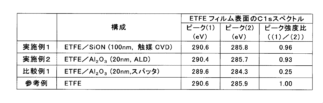

表1および図1に示すとおり、スパッタリング法によりガスバリア層を形成した比較例1では、ピーク(1)および(2)のそれぞれの位置が、参考例に比べてマイナス方向に大きくシフトしていた。また、ピーク強度比も大きく低下していた。一方、触媒CVD法またはALD法によりガスバリア層を形成した実施例1~2では、それらのピークのシフトはほとんど生じていなかった。また、実施例1~2のピーク強度比は、0.93以上と高く、参考例のピーク強度比(1.00)と比べてもほとんど変化は見られなかった。
そして表2に示すとおり、実施例1~2の積層体は、初期、耐候性試験後ともに、高い密着強度を有しており、水蒸気バリア性も高かった。一方、比較例1の積層体は、水蒸気バリア性は高いものの、初期の時点で密着性が低かった。
そして表2に示すとおり、実施例1~2の積層体は、初期、耐候性試験後ともに、高い密着強度を有しており、水蒸気バリア性も高かった。一方、比較例1の積層体は、水蒸気バリア性は高いものの、初期の時点で密着性が低かった。
本発明の積層体は、耐候性、ガスバリア性に優れ、層間の密着性およびその耐久性にも優れており、太陽電池モジュール用保護シートとして有用である。また、本発明の積層体は、太陽電池モジュール用保護シートに限定されるものではなく、耐候性やガスバリア性が要求される種々の用途に利用できる。このような用途としては、たとえば、ディスプレイ用保護シート、有機EL照明の保護フィルム部材、有機ELディスプレイ保護フィルム部材、電子ペーパー保護フィルム部材、太陽熱発電用ミラー保護部材、食品包装部材、医薬品包装部材等が挙げられる。
なお、2010年8月13日に出願された日本特許出願2010-181207号の明細書、特許請求の範囲、図面及び要約書の全内容をここに引用し、本発明の明細書の開示として、取り入れるものである。
なお、2010年8月13日に出願された日本特許出願2010-181207号の明細書、特許請求の範囲、図面及び要約書の全内容をここに引用し、本発明の明細書の開示として、取り入れるものである。
1…チャンバー(真空容器)、2…第一の原料ガス供給部、3…第二の原料ガス供給部、4…触媒体、5…基材ホルダー、6…ターボ分子ポンプ、7…ロータリーポンプ、10…成膜装置、11…チャンバー(真空容器)、12…原料ガス供給ライン、13…反応性ガス供給ライン、14…パージガス供給ライン、15…基材ホルダー、16…ロータリーポンプ、20…成膜装置
Claims (9)
- フッ素樹脂を含有する基材シートの少なくとも片面上に、酸素、窒素および炭素からなる群から選ばれる少なくとも1種と、金属とから構成される無機化合物を主成分とするガスバリア層が直接積層された積層体であり、
前記ガスバリア層の積層面における前記基材シートのX線光電子分光法により測定されるC1sスペクトルにおいて、結合エネルギー289~291eVの範囲内に有する最大ピークの位置が、290.1~290.6eVの範囲内であることを特徴とする積層体。 - 前記フッ素樹脂が、エチレン-テトラフルオロエチレン共重合体を含む、請求項1に記載の積層体。
- 前記ガスバリア層の積層面における前記基材シートのX線光電子分光法により測定されるC1sスペクトルにおいて、結合エネルギー284~286eVの範囲内に有する最大ピークの位置が、285.0~285.9eVの範囲内である、請求項1又は2に記載の積層体。
- 前記無機化合物が、Si化合物およびAl化合物からなる群から選ばれる少なくとも1種含む、請求項1~3のいずれか一項に記載の積層体。
- 前記無機化合物が、酸化ケイ素、窒化ケイ素、酸化窒化ケイ素、酸化窒化炭化ケイ素および酸化アルミニウムからなる群から選ばれる少なくとも1種を含む、請求項4に記載の積層体。
- 太陽電池モジュール用保護シートである、請求項1~5のいずれか一項に記載の積層体。
- フッ素樹脂を含有する基材シートの少なくとも片面上に、触媒化学蒸着法により、酸素、窒素および炭素からなる群から選ばれる少なくとも1種と、金属とから構成される無機化合物を主成分とするガスバリア層を形成し、前記基材シートと前記ガスバリア層とが直接積層された積層体を製造することを特徴する製造方法。
- フッ素樹脂を含有する基材シートの少なくとも片面上に、原子層堆積法により、酸素、窒素および炭素からなる群から選ばれる少なくとも1種と、金属とから構成される無機化合物を主成分とするガスバリア層を形成し、前記基材シートと前記ガスバリア層とが直接積層された積層体を製造することを特徴する製造方法。
- 前記金属が、ケイ素またはアルミニウムである請求項7または8に記載の製造方法。
Priority Applications (4)
| Application Number | Priority Date | Filing Date | Title |
|---|---|---|---|
| CN2011800391245A CN103079807A (zh) | 2010-08-13 | 2011-08-09 | 层叠体和层叠体的制造方法 |
| EP11816435.9A EP2604427A4 (en) | 2010-08-13 | 2011-08-09 | LAMINATE AND LAMINATE MANUFACTURING METHOD |
| JP2012528690A JPWO2012020771A1 (ja) | 2010-08-13 | 2011-08-09 | 積層体および積層体の製造方法 |
| US13/765,171 US20130157062A1 (en) | 2010-08-13 | 2013-02-12 | Laminate and process for producing laminate |
Applications Claiming Priority (2)
| Application Number | Priority Date | Filing Date | Title |
|---|---|---|---|
| JP2010-181207 | 2010-08-13 | ||
| JP2010181207 | 2010-08-13 |
Related Child Applications (1)
| Application Number | Title | Priority Date | Filing Date |
|---|---|---|---|
| US13/765,171 Continuation US20130157062A1 (en) | 2010-08-13 | 2013-02-12 | Laminate and process for producing laminate |
Publications (1)
| Publication Number | Publication Date |
|---|---|
| WO2012020771A1 true WO2012020771A1 (ja) | 2012-02-16 |
Family
ID=45567733
Family Applications (1)
| Application Number | Title | Priority Date | Filing Date |
|---|---|---|---|
| PCT/JP2011/068191 Ceased WO2012020771A1 (ja) | 2010-08-13 | 2011-08-09 | 積層体および積層体の製造方法 |
Country Status (6)
| Country | Link |
|---|---|
| US (1) | US20130157062A1 (ja) |
| EP (1) | EP2604427A4 (ja) |
| JP (1) | JPWO2012020771A1 (ja) |
| CN (1) | CN103079807A (ja) |
| TW (1) | TW201213145A (ja) |
| WO (1) | WO2012020771A1 (ja) |
Cited By (3)
| Publication number | Priority date | Publication date | Assignee | Title |
|---|---|---|---|---|
| JP2016515166A (ja) * | 2013-02-27 | 2016-05-26 | ロータス アプライド テクノロジー エルエルシーLotus Applied Technology, Llc | 混合金属‐シリコン‐酸化物バリア |
| US10202693B2 (en) | 2014-05-27 | 2019-02-12 | Panasonic Intellectual Property Management Co., Ltd. | Gas barrier film, film substrate provided with gas barrier film, and electronic device including the film substrate |
| WO2019044088A1 (ja) * | 2017-08-31 | 2019-03-07 | 富士フイルム株式会社 | 太陽電池モジュール |
Families Citing this family (9)
| Publication number | Priority date | Publication date | Assignee | Title |
|---|---|---|---|---|
| JP6657588B2 (ja) * | 2015-04-17 | 2020-03-04 | 凸版印刷株式会社 | 積層体及びその製造方法 |
| US12180581B2 (en) | 2017-09-18 | 2024-12-31 | Waters Technologies Corporation | Use of vapor deposition coated flow paths for improved chromatography of metal interacting analytes |
| US12181452B2 (en) | 2017-09-18 | 2024-12-31 | Waters Technologies Corporation | Use of vapor deposition coated flow paths for improved chromatography of metal interacting analytes |
| US11709155B2 (en) | 2017-09-18 | 2023-07-25 | Waters Technologies Corporation | Use of vapor deposition coated flow paths for improved chromatography of metal interacting analytes |
| US11709156B2 (en) | 2017-09-18 | 2023-07-25 | Waters Technologies Corporation | Use of vapor deposition coated flow paths for improved analytical analysis |
| EP3930867B1 (en) | 2019-02-27 | 2025-11-12 | Waters Technologies Corporation | Chromatographic seal and coated flow paths for minimizing analyte adsorption |
| JP7326091B2 (ja) * | 2019-09-24 | 2023-08-15 | 東芝テック株式会社 | インクジェットヘッド及びインクジェットプリンタ |
| US11918936B2 (en) | 2020-01-17 | 2024-03-05 | Waters Technologies Corporation | Performance and dynamic range for oligonucleotide bioanalysis through reduction of non specific binding |
| US12352734B2 (en) | 2020-09-24 | 2025-07-08 | Waters Technologies Corporation | Chromatographic hardware improvements for separation of reactive molecules |
Citations (13)
| Publication number | Priority date | Publication date | Assignee | Title |
|---|---|---|---|---|
| JP2000138387A (ja) | 1998-10-29 | 2000-05-16 | Dainippon Printing Co Ltd | 太陽電池モジュ−ル用表面保護シ−トおよびそれを使用した太陽電池モジュ−ル |
| JP2000208795A (ja) | 1999-01-13 | 2000-07-28 | Dainippon Printing Co Ltd | 太陽電池モジュ―ル用表面保護シ―トおよびそれを使用した太陽電池モジュ―ル |
| JP2002161353A (ja) | 2000-10-23 | 2002-06-04 | Asm Microchemistry Oy | 酸化アルミニウムフィルムの低温での製造方法 |
| JP2004315899A (ja) | 2003-04-16 | 2004-11-11 | Mitsui Chemicals Inc | ガスバリア膜形成方法 |
| JP2004535514A (ja) * | 2001-07-18 | 2004-11-25 | ザ・リージエンツ・オブ・ザ・ユニバーシテイ・オブ・コロラド | 有機ポリマー表面に無機薄膜を成膜する方法 |
| JP2005535788A (ja) * | 2002-05-09 | 2005-11-24 | マサチューセッツ・インスティチュート・オブ・テクノロジー | 熱フィラメント化学蒸着による非対称膜の製造 |
| JP2006057121A (ja) | 2004-08-18 | 2006-03-02 | Kuraray Co Ltd | 窒化シリコン膜の製造方法及び表示装置用フィルム |
| JP2007152772A (ja) | 2005-12-06 | 2007-06-21 | Dainippon Printing Co Ltd | ガスバリアフィルム、およびその製造方法 |
| JP2008172244A (ja) * | 2007-01-09 | 2008-07-24 | Korea Electronics Telecommun | 電子素子用ZnO半導体膜の形成方法及び前記半導体膜を含む薄膜トランジスタ |
| JP2008230098A (ja) * | 2007-03-22 | 2008-10-02 | Mitsubishi Plastics Ind Ltd | ガスバリア積層フィルムとその製造方法。 |
| JP2009031612A (ja) * | 2007-07-27 | 2009-02-12 | Ulvac Japan Ltd | 樹脂基板 |
| JP2010181207A (ja) | 2009-02-03 | 2010-08-19 | Toyota Motor Corp | 力学量検出素子、及びその製造方法 |
| JP2010247417A (ja) * | 2009-04-15 | 2010-11-04 | Sumitomo Metal Mining Co Ltd | 金属ベース層付耐熱性樹脂フィルムと金属膜付耐熱性樹脂フィルムの製造方法および金属ベース層付耐熱性樹脂フィルムの製造装置 |
Family Cites Families (16)
| Publication number | Priority date | Publication date | Assignee | Title |
|---|---|---|---|---|
| US5593794A (en) * | 1995-01-23 | 1997-01-14 | Duracell Inc. | Moisture barrier composite film of silicon nitride and fluorocarbon polymer and its use with an on-cell tester for an electrochemical cell |
| JP2004217966A (ja) * | 2003-01-10 | 2004-08-05 | Mitsui Chemicals Inc | ガスバリア膜形成方法および装置 |
| US6894928B2 (en) * | 2003-01-28 | 2005-05-17 | Intersil Americas Inc. | Output voltage compensating circuit and method for a floating gate reference voltage generator |
| JP2005114876A (ja) * | 2003-10-03 | 2005-04-28 | Mitsui Chemicals Inc | 反射防止フィルム |
| JP2005310861A (ja) * | 2004-04-19 | 2005-11-04 | Mitsui Chemicals Inc | 炭化窒化珪素膜の形成方法 |
| JPWO2007111075A1 (ja) * | 2006-03-24 | 2009-08-06 | コニカミノルタエムジー株式会社 | 透明バリア性シート及び透明バリア性シートの製造方法 |
| JPWO2007111074A1 (ja) * | 2006-03-24 | 2009-08-06 | コニカミノルタエムジー株式会社 | 透明バリア性シート及び透明バリア性シートの製造方法 |
| JPWO2007111098A1 (ja) * | 2006-03-24 | 2009-08-06 | コニカミノルタエムジー株式会社 | 透明バリア性シート及びその製造方法 |
| JPWO2007111076A1 (ja) * | 2006-03-24 | 2009-08-06 | コニカミノルタエムジー株式会社 | 透明バリア性シートおよび透明バリア性シートの製造方法 |
| JPWO2007111092A1 (ja) * | 2006-03-24 | 2009-08-06 | コニカミノルタエムジー株式会社 | 透明バリア性シートおよび透明バリア性シートの製造方法 |
| JP2008208440A (ja) * | 2007-02-27 | 2008-09-11 | Tohcello Co Ltd | 薄膜の製造方法 |
| WO2010065564A1 (en) * | 2008-12-02 | 2010-06-10 | Georgia Tech Research Corporation | Environmental barrier coating for organic semiconductor devices and methods thereof |
| JP5470969B2 (ja) * | 2009-03-30 | 2014-04-16 | 株式会社マテリアルデザインファクトリ− | ガスバリアフィルム、それを含む電子デバイス、ガスバリア袋、およびガスバリアフィルムの製造方法 |
| JP2010274562A (ja) * | 2009-05-29 | 2010-12-09 | Fujifilm Corp | ガスバリア積層体およびガスバリア積層体の製造方法 |
| CN102484160A (zh) * | 2009-08-24 | 2012-05-30 | 纳幕尔杜邦公司 | 用于薄膜光伏电池的阻挡膜 |
| WO2012147571A1 (ja) * | 2011-04-27 | 2012-11-01 | 旭硝子株式会社 | 積層体の製造方法 |
-
2011
- 2011-08-09 WO PCT/JP2011/068191 patent/WO2012020771A1/ja not_active Ceased
- 2011-08-09 CN CN2011800391245A patent/CN103079807A/zh active Pending
- 2011-08-09 JP JP2012528690A patent/JPWO2012020771A1/ja active Pending
- 2011-08-09 EP EP11816435.9A patent/EP2604427A4/en not_active Withdrawn
- 2011-08-10 TW TW100128542A patent/TW201213145A/zh unknown
-
2013
- 2013-02-12 US US13/765,171 patent/US20130157062A1/en not_active Abandoned
Patent Citations (13)
| Publication number | Priority date | Publication date | Assignee | Title |
|---|---|---|---|---|
| JP2000138387A (ja) | 1998-10-29 | 2000-05-16 | Dainippon Printing Co Ltd | 太陽電池モジュ−ル用表面保護シ−トおよびそれを使用した太陽電池モジュ−ル |
| JP2000208795A (ja) | 1999-01-13 | 2000-07-28 | Dainippon Printing Co Ltd | 太陽電池モジュ―ル用表面保護シ―トおよびそれを使用した太陽電池モジュ―ル |
| JP2002161353A (ja) | 2000-10-23 | 2002-06-04 | Asm Microchemistry Oy | 酸化アルミニウムフィルムの低温での製造方法 |
| JP2004535514A (ja) * | 2001-07-18 | 2004-11-25 | ザ・リージエンツ・オブ・ザ・ユニバーシテイ・オブ・コロラド | 有機ポリマー表面に無機薄膜を成膜する方法 |
| JP2005535788A (ja) * | 2002-05-09 | 2005-11-24 | マサチューセッツ・インスティチュート・オブ・テクノロジー | 熱フィラメント化学蒸着による非対称膜の製造 |
| JP2004315899A (ja) | 2003-04-16 | 2004-11-11 | Mitsui Chemicals Inc | ガスバリア膜形成方法 |
| JP2006057121A (ja) | 2004-08-18 | 2006-03-02 | Kuraray Co Ltd | 窒化シリコン膜の製造方法及び表示装置用フィルム |
| JP2007152772A (ja) | 2005-12-06 | 2007-06-21 | Dainippon Printing Co Ltd | ガスバリアフィルム、およびその製造方法 |
| JP2008172244A (ja) * | 2007-01-09 | 2008-07-24 | Korea Electronics Telecommun | 電子素子用ZnO半導体膜の形成方法及び前記半導体膜を含む薄膜トランジスタ |
| JP2008230098A (ja) * | 2007-03-22 | 2008-10-02 | Mitsubishi Plastics Ind Ltd | ガスバリア積層フィルムとその製造方法。 |
| JP2009031612A (ja) * | 2007-07-27 | 2009-02-12 | Ulvac Japan Ltd | 樹脂基板 |
| JP2010181207A (ja) | 2009-02-03 | 2010-08-19 | Toyota Motor Corp | 力学量検出素子、及びその製造方法 |
| JP2010247417A (ja) * | 2009-04-15 | 2010-11-04 | Sumitomo Metal Mining Co Ltd | 金属ベース層付耐熱性樹脂フィルムと金属膜付耐熱性樹脂フィルムの製造方法および金属ベース層付耐熱性樹脂フィルムの製造装置 |
Non-Patent Citations (1)
| Title |
|---|
| See also references of EP2604427A4 |
Cited By (3)
| Publication number | Priority date | Publication date | Assignee | Title |
|---|---|---|---|---|
| JP2016515166A (ja) * | 2013-02-27 | 2016-05-26 | ロータス アプライド テクノロジー エルエルシーLotus Applied Technology, Llc | 混合金属‐シリコン‐酸化物バリア |
| US10202693B2 (en) | 2014-05-27 | 2019-02-12 | Panasonic Intellectual Property Management Co., Ltd. | Gas barrier film, film substrate provided with gas barrier film, and electronic device including the film substrate |
| WO2019044088A1 (ja) * | 2017-08-31 | 2019-03-07 | 富士フイルム株式会社 | 太陽電池モジュール |
Also Published As
| Publication number | Publication date |
|---|---|
| US20130157062A1 (en) | 2013-06-20 |
| TW201213145A (en) | 2012-04-01 |
| EP2604427A1 (en) | 2013-06-19 |
| EP2604427A4 (en) | 2014-12-24 |
| JPWO2012020771A1 (ja) | 2013-10-28 |
| CN103079807A (zh) | 2013-05-01 |
Similar Documents
| Publication | Publication Date | Title |
|---|---|---|
| WO2012020771A1 (ja) | 積層体および積層体の製造方法 | |
| WO2011004872A1 (ja) | 太陽電池モジュール用保護シート | |
| WO2011108609A1 (ja) | 積層体およびその製造方法 | |
| TW201206700A (en) | Encapsulation film, package structure utilizing the same, and method for forming the package structure | |
| WO2019044088A1 (ja) | 太陽電池モジュール | |
| US20090305062A1 (en) | Method for fabricating multilayered encapsulation thin film having optical functionality and mutilayered encapsulation thin film fabricated by the same | |
| US8586174B2 (en) | Laminate and process for its production | |
| JP6737279B2 (ja) | 電子デバイス及び電子デバイスの封止方法 | |
| JP2013202822A (ja) | ガスバリア性積層フィルム | |
| JP2018525257A (ja) | 多層バリアアセンブリを含む複合材物品及びその製造方法 | |
| JP2005256061A (ja) | 積層体 | |
| JP2010219196A (ja) | 太陽電池モジュール用裏面保護シート及び太陽電池モジュール | |
| WO2012147571A1 (ja) | 積層体の製造方法 | |
| JP2018525253A (ja) | 複合材物品及その製造方法 | |
| JP2001007368A (ja) | 太陽電池モジュ−ル用保護シ−トおよびそれを使用した太陽電池モジュ−ル | |
| JP2010238816A (ja) | 太陽電池モジュール用保護シート、及びそれを用いてなる太陽電池モジュール | |
| WO2011118383A1 (ja) | 積層体およびその製造方法 | |
| JP6909780B2 (ja) | 多層バリアアセンブリを含む複合材物品及びその製造方法 | |
| JP2011042835A (ja) | ガスバリアフィルムおよびその製造方法 |
Legal Events
| Date | Code | Title | Description |
|---|---|---|---|
| WWE | Wipo information: entry into national phase |
Ref document number: 201180039124.5 Country of ref document: CN |
|
| 121 | Ep: the epo has been informed by wipo that ep was designated in this application |
Ref document number: 11816435 Country of ref document: EP Kind code of ref document: A1 |
|
| WWE | Wipo information: entry into national phase |
Ref document number: 2012528690 Country of ref document: JP |
|
| NENP | Non-entry into the national phase |
Ref country code: DE |
|
| WWE | Wipo information: entry into national phase |
Ref document number: 2011816435 Country of ref document: EP |