WO2012029210A1 - 増幅装置 - Google Patents
増幅装置 Download PDFInfo
- Publication number
- WO2012029210A1 WO2012029210A1 PCT/JP2011/002675 JP2011002675W WO2012029210A1 WO 2012029210 A1 WO2012029210 A1 WO 2012029210A1 JP 2011002675 W JP2011002675 W JP 2011002675W WO 2012029210 A1 WO2012029210 A1 WO 2012029210A1
- Authority
- WO
- WIPO (PCT)
- Prior art keywords
- signal
- input
- voltage value
- voltage
- converter
- Prior art date
- Legal status (The legal status is an assumption and is not a legal conclusion. Google has not performed a legal analysis and makes no representation as to the accuracy of the status listed.)
- Ceased
Links
Images


Classifications
-
- H—ELECTRICITY
- H03—ELECTRONIC CIRCUITRY
- H03F—AMPLIFIERS
- H03F3/00—Amplifiers with only discharge tubes or only semiconductor devices as amplifying elements
- H03F3/181—Low-frequency amplifiers, e.g. audio preamplifiers
- H03F3/183—Low-frequency amplifiers, e.g. audio preamplifiers with semiconductor devices only
- H03F3/185—Low-frequency amplifiers, e.g. audio preamplifiers with semiconductor devices only with field-effect devices
-
- H—ELECTRICITY
- H03—ELECTRONIC CIRCUITRY
- H03F—AMPLIFIERS
- H03F1/00—Details of amplifiers with only discharge tubes, only semiconductor devices or only unspecified devices as amplifying elements
- H03F1/02—Modifications of amplifiers to raise the efficiency, e.g. gliding Class A stages, use of an auxiliary oscillation
- H03F1/0205—Modifications of amplifiers to raise the efficiency, e.g. gliding Class A stages, use of an auxiliary oscillation in transistor amplifiers
- H03F1/0211—Modifications of amplifiers to raise the efficiency, e.g. gliding Class A stages, use of an auxiliary oscillation in transistor amplifiers with control of the supply voltage or current
-
- H—ELECTRICITY
- H03—ELECTRONIC CIRCUITRY
- H03F—AMPLIFIERS
- H03F1/00—Details of amplifiers with only discharge tubes, only semiconductor devices or only unspecified devices as amplifying elements
- H03F1/02—Modifications of amplifiers to raise the efficiency, e.g. gliding Class A stages, use of an auxiliary oscillation
- H03F1/0205—Modifications of amplifiers to raise the efficiency, e.g. gliding Class A stages, use of an auxiliary oscillation in transistor amplifiers
- H03F1/0211—Modifications of amplifiers to raise the efficiency, e.g. gliding Class A stages, use of an auxiliary oscillation in transistor amplifiers with control of the supply voltage or current
- H03F1/0216—Continuous control
- H03F1/0222—Continuous control by using a signal derived from the input signal
-
- H—ELECTRICITY
- H03—ELECTRONIC CIRCUITRY
- H03F—AMPLIFIERS
- H03F1/00—Details of amplifiers with only discharge tubes, only semiconductor devices or only unspecified devices as amplifying elements
- H03F1/32—Modifications of amplifiers to reduce non-linear distortion
- H03F1/3205—Modifications of amplifiers to reduce non-linear distortion in field-effect transistor amplifiers
-
- H—ELECTRICITY
- H03—ELECTRONIC CIRCUITRY
- H03F—AMPLIFIERS
- H03F3/00—Amplifiers with only discharge tubes or only semiconductor devices as amplifying elements
- H03F3/181—Low-frequency amplifiers, e.g. audio preamplifiers
- H03F3/183—Low-frequency amplifiers, e.g. audio preamplifiers with semiconductor devices only
- H03F3/185—Low-frequency amplifiers, e.g. audio preamplifiers with semiconductor devices only with field-effect devices
- H03F3/1855—Low-frequency amplifiers, e.g. audio preamplifiers with semiconductor devices only with field-effect devices with junction-FET devices
-
- H—ELECTRICITY
- H03—ELECTRONIC CIRCUITRY
- H03F—AMPLIFIERS
- H03F3/00—Amplifiers with only discharge tubes or only semiconductor devices as amplifying elements
- H03F3/20—Power amplifiers, e.g. Class B amplifiers, Class C amplifiers
- H03F3/21—Power amplifiers, e.g. Class B amplifiers, Class C amplifiers with semiconductor devices only
- H03F3/217—Class D power amplifiers; Switching amplifiers
- H03F3/2173—Class D power amplifiers; Switching amplifiers of the bridge type
-
- H—ELECTRICITY
- H03—ELECTRONIC CIRCUITRY
- H03F—AMPLIFIERS
- H03F2200/00—Indexing scheme relating to amplifiers
- H03F2200/171—A filter circuit coupled to the output of an amplifier
-
- H—ELECTRICITY
- H03—ELECTRONIC CIRCUITRY
- H03F—AMPLIFIERS
- H03F2200/00—Indexing scheme relating to amplifiers
- H03F2200/504—Indexing scheme relating to amplifiers the supply voltage or current being continuously controlled by a controlling signal, e.g. the controlling signal of a transistor implemented as variable resistor in a supply path for, an IC-block showed amplifier
Definitions
- the present invention relates to an amplifying apparatus for inputting a digital signal, and more particularly to an amplifying apparatus for improving the S / N of the output signal and improving the distortion by negatively feeding back the output signal to the digital signal input unit.
- a voltage variable power supply is used as a power supply for an amplifying device, and the power supply voltage value supplied to the power amplification stage is increased or decreased by following the input audio signal level to the amplifying device.
- the power supply voltage supplied to the power amplification stage follow the input audio signal level, when the input audio signal level is low, the power supply voltage of the power amplification stage is such that the amplified signal does not distort. Since the noise superimposed on the output signal of the amplifying device is reduced, the power efficiency of the power supply can be improved.
- noise and distortion superimposed on the output signal can be corrected by negatively feeding back the output signal to the signal input unit.
- an analog / digital converter that attenuates the amplified output signal to a predetermined voltage level and then converts the analog signal into a digital signal.
- an A / D converter is necessary for the negative feedback circuit, but due to the quantization error caused by the conversion accuracy of the A / D converter, the amount of correction of noise and distortion corrected by the negative feedback is reduced. There was a problem that correction was not made for the quantization error.
- an amplifying apparatus having a negative feedback circuit a high-speed conversion operation is required for the A / D converter inserted in the negative feedback circuit in order to ensure a stable operation of the amplifying apparatus.
- an A / D converter capable of high-speed conversion operation has a problem that conversion accuracy cannot be secured due to a theoretical limit of conversion processing capability.
- the present invention has been made to solve the conventional problems, and uses a voltage variable power supply as a power supply to increase or decrease the power supply voltage value supplied to the power amplification stage by following the input audio signal level to the amplifier.
- the amplifying apparatus when the voltage value of the power supply power of the power amplification stage is changed, the reference voltage value supplied to the A / D converter of the negative feedback circuit is controlled, so that the quantum caused by the conversion accuracy in the A / D converter circuit It is an object of the present invention to provide an amplifying apparatus that can reduce a conversion error and can improve an S / N and a distortion rate particularly when the input audio signal is small.
- an amplifying apparatus of the present invention detects the amplitude level of an input audio signal that has been input, and outputs a power having a voltage value indicated by target setting voltage value information corresponding to the detected amplitude level.
- a low-pass filter unit hereinafter referred to as LPF unit
- LPF unit low-pass filter unit that demodulates the amplified PWM signal into an acoustic signal, and the acoustic signal demodulated by the LPF unit is attenuated and then converted into a digital signal by an A / D converter.
- a negative feedback unit that performs negative feedback to the PWM modulation unit; and a voltage conversion unit that outputs a voltage proportional to a voltage value of the power output from the power supply voltage control unit, and the power output from the voltage conversion unit.
- The has a configuration using as a reference voltage value of the A / D converter.
- the conversion accuracy of the A / D converter in the negative feedback circuit can be kept high, and even when the input signal is particularly small compared to the prior art, By reducing the conversion error in the negative feedback circuit, the S / N and distortion rate of the output signal can be improved.
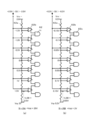
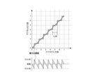
- Block diagram of amplifying apparatus 1 in an embodiment of the present invention The block diagram of the voltage conversion part 10 in embodiment of this invention Configuration diagram of A / D converter 62 in the embodiment of the present invention It is a figure explaining the state which changed the reference voltage value of the A / D converter 62 in embodiment of this invention, Comprising: (a) is a case where the power supply voltage supplied to the power amplification stage 4 is +/- 20V.
- FIG. 8B is a diagram showing a case where the power supply voltage supplied to the power amplification stage 4 is ⁇ 2V. The figure explaining the magnitude
- the amplifying apparatus 1 of the present embodiment is connected to an audio apparatus 8 that outputs a digital audio signal.
- the audio signal output from the audio device 8 is input to the amplifying device 1 as the input audio signal S1 of the amplifying device 1, and is amplified by the amplifying device 1 and output to the speaker 9.
- the speaker 9 converts the sound signal after power amplification output from the amplifying apparatus 1 into sound and emits the sound.
- the amplifying device 1 and the audio device 8 are connected to a DC power source (not shown) that supplies power necessary to operate them.
- a DC power source (not shown) that supplies power necessary to operate them.
- the power source required to operate each device is not limited to a DC power source, and an AC power source may be used as appropriate in accordance with the characteristics of each device.
- the audio device 8 and the amplifying device 1 are combined as an audio output device, and the audio output device and the speaker 9 are combined as an audio system device.
- the amplifying apparatus 1 includes a PWM conversion unit 2, a gate driver unit 3, a power amplification stage 4, an LPF unit 5, a negative feedback unit 6, a power supply voltage control unit 7, and a voltage conversion unit 10.
- the input audio signal S 1 is input to the power supply voltage control unit 7 and also to the PWM conversion unit 2.
- the power supply voltage control unit 7 detects the amplitude level of the input audio signal S1 input from the audio device 8, and obtains the gain correction value S8 corresponding to the detected amplitude level of the input audio signal S1 and the target set voltage value information S10.
- the gain correction value S8 is selected and output to the negative feedback unit 6, and the output voltages on the positive side and the negative side are controlled so that the target voltage is the voltage value indicated by the target setting voltage value information S10.
- the power supply power that is the positive and negative voltage values is sent to the power amplification stage 4.
- the PWM conversion unit 2 calculates a differential signal including an error component between the corrected digital feedback signal S7 input from the negative feedback unit 6 and the input audio signal S1 input from the audio device 8, and converts the difference signal into the PWM signal S2. To the gate driver unit 3.
- a PWM conversion method As a PWM conversion method, a delta-sigma conversion method, a triangular wave comparison method, and the like are known, and any of these methods is also applied in the present embodiment.
- the PWM conversion unit 2 can be realized by a digital signal processor, a microcontroller, or the like.
- the gate driver unit 3 inserts a dead time into the input PWM signal S2 and creates a drive signal in which the potential of the PWM signal S2 is shifted to such an extent that the high-side and low-side high-speed switching elements of the power amplification stage 4 can be driven. Then, it is sent to the power amplification stage 4.
- the power amplification stage 4 includes a high-side high-speed switching element that is disposed on the high-potential power supply side and is supplied with a positive-side voltage from the power-supply voltage control section 7, and a power-supply voltage control section disposed on the low-potential power supply (or ground) side. 7 is composed of a half-bridge circuit including a low-side high-speed switching element to which a negative voltage is supplied.
- the power amplification stage 4 performs a high-speed switching operation with a voltage amplitude determined by the positive side voltage and the negative side voltage in accordance with the drive signal inputted from the gate driver unit 3, and the signal inputted to the power amplification stage 4 is converted into power. Amplification is performed to obtain an amplified PWM signal S3.
- the obtained amplified PWM signal S3 is input to the LPF unit 5.
- the high-speed switching element for example, a MOS field effect transistor or the like is used.
- the LPF unit 5 is a filter that outputs an amplified analog audio signal S4 obtained by removing unnecessary high frequency components from the amplified PWM signal S3 output from the power amplification stage 4 to the speaker 9 and the negative feedback unit 6, for example. It is composed of elements such as coils and capacitors.
- the negative feedback unit 6 attenuates the amplified analog audio signal S4 output from the LPF unit 5, and converts the amplified analog audio signal S4 into a digital signal using the positive reference voltage value Vrp and the negative reference voltage value Vrn input from the voltage conversion unit 10. Then, after correcting the magnitude of the digital signal converted at a predetermined ratio, it is negatively fed back to the PWM converter 2 as a corrected digital feedback signal S7.
- the amplifying apparatus 1 in the present embodiment is configured such that the amplified analog audio signal S4 output from the LPF unit 5 is input to the negative feedback unit 6.
- the amplified PWM signal S3 output from the power amplification stage 4 is not input to the negative feedback unit 6, but the amplified analog audio signal S4 output from the LPF unit 5 is input to the negative feedback unit 6.
- distortion generated in the LPF unit 5 is also corrected by negative feedback, and the distortion rate can be further improved.
- the voltage conversion unit 10 receives the positive side voltage value + Vdd and negative side voltage value ⁇ Vdd of the power source power supplied to the power amplification stage 4 and inputs the input positive side voltage value + Vdd and negative side voltage value ⁇ Vdd in advance.
- the positive reference voltage value Vrp and the negative reference voltage value Vrn are generated by stepping down at a predetermined ratio set, and the generated positive reference voltage value Vrp and the negative reference voltage value Vrn are output to the negative feedback unit 6. .
- the voltage conversion unit 10 is most simply realized by two sets of two resistance elements connected in series as shown in FIG. 2, and the resistance values of the two resistance elements (10a, 10b, and 10c, 10d).
- the positive side voltage value + Vdd and the negative side voltage value ⁇ Vdd are stepped down at the ratios of Ra and Rb, and Rc and Rd, respectively, to create the positive side reference voltage value Vrp and the negative side reference voltage value Vrn.
- the positive reference voltage value Vrp and the negative reference voltage value Vrn are output to the negative feedback unit 6 from the connection point of.
- the power supply voltage control unit 7 includes an input signal level detection unit 71, a control unit 72, and a voltage variable power supply unit 73.
- the input signal level detection unit 71 creates input signal amplitude level information S9 including amplitude information of the input audio signal S1 input from the audio device 8 and sends it to the control unit 72.
- the control unit 72 includes target set voltage value information S10 and gain correction corresponding to the input signal amplitude level information S9 created by the input signal level detection unit 71 from the data table information preset in the control unit 72.
- the value S8 is selected, and the selected target set voltage value information S10 is output to the voltage variable power supply unit 73, and the gain correction value S8 is output to the negative feedback unit 6.
- the target set voltage value information S10 is information indicating the target value of the voltage value to be set for the voltage variable power supply unit 73, and the gain correction value S8 is set in advance according to the target value of the voltage value to be set. This is information indicating the corrected constant.
- the voltage variable power source unit 73 is a power source that varies the output voltage to a voltage value to be set according to the target set voltage value information S10 input from the control unit 72, and is controlled based on the target set voltage value information S10.
- the power supply power having a voltage value is supplied to the power amplification stage 4.
- the input signal level detection unit 71 and the control unit 72 can be realized by a digital signal processor, a microcontroller, or the like.
- the negative feedback unit 6 includes an attenuator 61, an A / D converter 62, and a gain correction unit 63.
- the attenuator 61 receives the amplified analog audio signal S4 output from the LPF unit 5, generates an attenuated analog feedback signal S5 that is attenuated at a preset ratio, and generates the attenuated analog feedback signal S5 in the A / D converter 62 The attenuated analog feedback signal S5 is output.
- the attenuator 61 is realized by two resistance elements connected in series, and attenuates the amplified analog audio signal S4 at a ratio of preset resistance values of the two resistance elements.
- the A / D converter 62 receives the attenuated analog feedback signal S5 output from the attenuator 61, the positive reference voltage value Vrp and the negative reference voltage value Vrn output from the voltage conversion unit 10, respectively.
- a digital value is obtained from a result obtained by comparing a reference voltage value (detailed later) created by dividing the reference voltage value Vrp and the negative side reference voltage value Vrn at a predetermined ratio with the input attenuated analog feedback signal S5.
- a feedback signal S6 is generated, and the generated digital feedback signal S6 is output to the gain correction unit 63.
- the A / D converter 62 includes at least a plurality of connected resistance elements and capacitor arrays, and is defined as a converter that compares a reference voltage value with an input analog signal.
- Systems such as series-parallel type and sub-ranging type are known.
- the gain correction unit 63 receives the digital feedback signal S6 output from the A / D converter 62 and the gain correction value S8 output from the control unit 72, respectively, and the digital feedback signal S6 corresponding to the gain correction value S8.
- the corrected digital feedback signal S7 is output to the PWM converter 2.
- the gain correction unit 63 can be realized by a multiplier provided in a digital signal processor, a microcontroller, or the like.
- a reference resistor string 62a in which unit resistors R1 to R8 are connected in series, and connection point potentials Vr1 to Vr7 of each unit resistor of the reference resistor string 62a are input.
- Comparator group 62b for comparing the potential of the attenuated analog feedback signal (the comparators are shown as C1 to C7 in the figure), and a logic circuit group 62c to which the comparison result output of the comparator group 62b is input (each logic circuit in the figure)
- an encoder 62d that converts each output of the logic circuit group 62c into data of a predetermined number of bits.
- One end of the reference resistor string 62a is connected to the positive reference voltage value Vrp output from the voltage converter 10, and the other end is connected to the negative reference voltage value Vrn.
- a clock signal is input to each of the comparators C1 to C7 of the comparator group 62b from an external clock circuit (not shown in the figure).
- the input to one terminal is the connection point potentials Vr1 to Vr7 of each unit resistor of the reference resistor array 62a, and the potential of the attenuated analog feedback signal S5 input to the other terminal
- the potential of the attenuated analog feedback signal S5 is larger than the connection point potentials Vr1 to Vr7, 1 is output and the potential of the attenuated analog feedback signal S5 is smaller than the connection point potentials Vr1 to Vr7. 0 is output to.
- the outputs of the comparators C1 to C7 are latched at the rising edge of the clock signal, and the output state is fixed (held).
- Each of the logic circuits D1 to D7 of the logic circuit group 62c is obtained as a result of logical product with respect to the two terminal inputs by receiving the forward and inversion outputs from the comparators C1 to C7 of the adjacent comparator group 62b. Is output to the encoder 62d.
- the encoder 62d converts the input outputs of the logic circuits D1 to D7 into data of a predetermined number of bits and outputs the data.
- the quantization generated in the parallel A / D converter 62 by variably controlling the positive reference voltage value Vrp and the negative reference voltage value Vrn of the parallel A / D converter 62 given as an example.
- the operation for reducing the instantaneous value of the error will be described with reference to FIGS.
- Quantization is the conversion of an analog signal into a digital signal, and is defined as converting a continuous analog value into a discrete digital value.
- the width of the analog value of one digital value is 1LSB, as shown in the figure, the range of 1LSB of consecutive analog values is all output as the same digital value, so 0.5LSB from the center of 1LSB
- the instantaneous value of the error is the largest.
- the quantization error is distributed in a range of ⁇ 0.5LSB with the center of 1LSB being 0, and if 1LSB is large, the quantization error is also large.
- FIG. 4 shows a case where the parallel-side A / D converter 62 has a positive voltage value + Vdd of the power supply power supplied to the power amplification stage 4 of 20 V and a negative voltage value of ⁇ Vdd of ⁇ 20 V as case A (FIG. 4 (a)), the case where the positive side voltage value + Vdd is 2V and the negative side voltage value ⁇ Vdd is ⁇ 2V is referred to as case B (FIG. 4B), and two cases are shown.
- the predetermined ratio at which the voltage conversion unit 10 steps down the voltage value of the power supply is 1/10.
- Case A is a case where the positive side voltage value + Vdd of the power source power supplied to the power amplification stage 4 is 20V, and 2V of the voltage value obtained by stepping down + Vdd from the voltage conversion unit 10 at a ratio of 1/10 is the positive side reference. It is input as a voltage value Vrp.
- a voltage value of ⁇ 2 V obtained by stepping down the negative side voltage value ⁇ Vdd of the power source power by a ratio of 1/10 is input from the voltage conversion unit 10 as the negative side reference voltage value Vrn.
- connection point potentials Vr1 to Vr7 of the reference resistor array 62a configured by connecting unit resistors in series are divided at equal intervals between the positive reference voltage value Vrp and the negative reference voltage value Vrn.
- the potential is 0.5V.
- the value of this adjacent connection point potential is set to 1LSB. In case A, 1LSB is 0.5V.
- Case B is a case where the positive voltage value + Vdd of the power source power supplied to the power amplification stage 4 is 2V, and a voltage value of 0.2V obtained by stepping down + Vdd from the voltage converter 10 at a ratio of 1/10 is positive. It is input as the side reference voltage value Vrp.
- a voltage value of ⁇ 0.2 V obtained by stepping down the negative side voltage value ⁇ Vdd of the power source power by a ratio of 1/10 is input from the voltage conversion unit 10 as the negative side reference voltage value Vrn.
- connection point potentials Vr1 to Vr7 of the reference resistor array 62a configured by connecting unit resistors in series are divided at equal intervals between the positive reference voltage value Vrp and the negative reference voltage value Vrn.
- the potential is 0.05V.
- 1LSB is 0.05V.
- the case of FIG. 4 is caused by the change in the reference voltage values Vrp and Vrn of the A / D converter 62 controlled in accordance with the amplitude level of the input audio signal S1.
- the instantaneous value of the quantization error is reduced in the case of Case B compared to the case A by the amount that the value of 1LSB changes from 0.5V to 0.05V. I understand that.
- the low-side high-speed switching element of the power amplification stage 4 is arranged on the low-potential power supply side, but it may be connected to the ground and the voltage variable power supply unit 73 may be a single output power supply. In this case, it is desirable to add a large capacity capacitor for DC cut between the power amplification stage 4 and the speaker 9.
- the voltage variable power supply unit 73 may be a single output power supply, and the power amplification stage 4 may be configured by a full bridge circuit.
- the set of resistance elements of the voltage converter 10 can be changed to one, and the analog reference voltage of the A / D converter 62 can be set to one. it can.
- the voltage variable power supply 73 is used as a power supply, and the power supply voltage value supplied to the power amplification stage 4 is made to follow the input audio signal level S1 to the amplifying apparatus 1.
- the amplifying apparatus 1 to be increased or decreased, when the voltage value of the power supply power of the power amplification stage 4 is changed, by controlling the reference voltage value supplied to the A / D converter 62 of the negative feedback circuit, the A / D converter circuit 62 It is possible to reduce the quantization error due to the conversion accuracy, and to improve the S / N and distortion rate particularly when the input audio signal is small.
- the amplifying apparatus of the present invention is useful as an amplifying apparatus for improving the S / N of the output signal and improving the distortion by negatively feeding back the amplified output signal to the digital signal input unit.
Landscapes
- Engineering & Computer Science (AREA)
- Power Engineering (AREA)
- Multimedia (AREA)
- Physics & Mathematics (AREA)
- Nonlinear Science (AREA)
- Amplifiers (AREA)
Abstract
Description
なお、オーディオ装置8と増幅装置1とを合わせてオーディオ出力装置、またオーディオ出力装置とスピーカ9とを合わせてオーディオシステム装置とする。
また、電圧可変電源部73を単出力電源にするとともに、電力増幅段4をフルブリッジ回路で構成してもよい。
そして、電圧可変電源部73を単出力電源にした場合、電圧変換器10の抵抗素子の組も1つに変更することができ、A/D変換器62のアナログ基準電圧も1つとすることができる。
2 PWM変換部
3 ゲートドライバ部
4 電力増幅段
5 LPF部
6 負帰還部
7 電源電圧制御部
8 オーディオ装置
9 スピーカ
10 電圧変換部
10a 抵抗Ra
10b 抵抗Rb
10c 抵抗Rc
10d 抵抗Rd
61 減衰器
62 A/D変換器
62a 基準抵抗列
62b コンパレータ群
62c 論理回路群
62d エンコーダ
63 ゲイン補正部
71 入力信号レベル検出部
72 コントロール部
73 電圧可変電源部
Claims (4)
- 入力された入力音声信号の振幅レベルを検出し、検出した前記振幅レベルに対応する目標設定電圧値情報が示す電圧値の電力を出力する電源電圧制御部と、
前記入力音声信号をパルス幅変調信号に変換するPWM変換部と、
前記PWM変換部から出力された前記パルス幅変調信号を電力増幅する電力増幅段と、
前記電力増幅段から出力された増幅PWM信号を音響信号に復調するローパスフィルタ部と、
前記ローパスフィルタ部で復調された前記音響信号を減衰させてからA/D変換器にてデジタル信号に変換して前記PWM変調部に負帰還する負帰還部と、
前記電源電圧制御部が出力した電力の電圧値に比例した電圧を出力する電圧変換部とを備え、
前記電圧変換部が出力した電圧を前記A/D変換器の基準電圧値として用いることを特徴とする増幅装置。 - 前記電圧変換部は、2組の直列に接続された2つの抵抗素子からなることを特徴とする請求項1記載の増幅装置。
- 入力音声信号を生成し出力するオーディオ装置と、
前記入力音声信号が入力される請求項1記載の増幅装置と、
を有するオーディオ出力装置。 - 請求項3のオーディオ出力装置と、
前記オーディオ出力装置から出力された前記音響信号が入力されるスピーカと、
を有するオーディオシステム装置。
Priority Applications (4)
| Application Number | Priority Date | Filing Date | Title |
|---|---|---|---|
| JP2012531655A JP5861076B2 (ja) | 2010-08-30 | 2011-05-13 | 増幅装置 |
| EP11821235.6A EP2613438B1 (en) | 2010-08-30 | 2011-05-13 | Amplifier |
| CN201180035773.8A CN103026618B (zh) | 2010-08-30 | 2011-05-13 | 放大装置 |
| US13/808,420 US9136799B2 (en) | 2010-08-30 | 2011-05-13 | Amplifier using voltage variable power supply |
Applications Claiming Priority (2)
| Application Number | Priority Date | Filing Date | Title |
|---|---|---|---|
| JP2010191812 | 2010-08-30 | ||
| JP2010-191812 | 2010-08-30 |
Publications (1)
| Publication Number | Publication Date |
|---|---|
| WO2012029210A1 true WO2012029210A1 (ja) | 2012-03-08 |
Family
ID=45772337
Family Applications (1)
| Application Number | Title | Priority Date | Filing Date |
|---|---|---|---|
| PCT/JP2011/002675 Ceased WO2012029210A1 (ja) | 2010-08-30 | 2011-05-13 | 増幅装置 |
Country Status (5)
| Country | Link |
|---|---|
| US (1) | US9136799B2 (ja) |
| EP (1) | EP2613438B1 (ja) |
| JP (1) | JP5861076B2 (ja) |
| CN (1) | CN103026618B (ja) |
| WO (1) | WO2012029210A1 (ja) |
Cited By (1)
| Publication number | Priority date | Publication date | Assignee | Title |
|---|---|---|---|---|
| CN103607176A (zh) * | 2013-10-21 | 2014-02-26 | 梁秀红 | 音频功放供电电路控制方法及音频功放供电电路及音频功放电路 |
Families Citing this family (11)
| Publication number | Priority date | Publication date | Assignee | Title |
|---|---|---|---|---|
| EP2587665B1 (en) * | 2010-06-25 | 2016-01-20 | Panasonic Intellectual Property Management Co., Ltd. | Amplifier apparatus |
| US9258641B2 (en) * | 2012-06-07 | 2016-02-09 | Qbiz, Llc | Method and system of audio capture based on logarithmic conversion |
| US9184705B2 (en) | 2013-03-15 | 2015-11-10 | Bose Corporation | Feedback mechanism for boost-on-demand amplifiers |
| US9154095B2 (en) * | 2013-03-15 | 2015-10-06 | Bose Corporation | Boost-on-demand amplifier |
| CN104104452B (zh) * | 2014-06-24 | 2016-08-24 | 努比亚技术有限公司 | 基于pwm调制的音频解调方法和解调器 |
| CN107179519A (zh) * | 2017-06-09 | 2017-09-19 | 中国电子科技集团公司第四十研究所 | 一种用于数字示波器的通道校准装置及方法 |
| US10763811B2 (en) * | 2018-07-25 | 2020-09-01 | Cirrus Logic, Inc. | Gain control in a class-D open-loop amplifier |
| US12334950B2 (en) * | 2022-12-28 | 2025-06-17 | Texas Instruments Incorporated | Dynamic range boost for amplifiers |
| TWI854417B (zh) * | 2022-12-28 | 2024-09-01 | 茂達電子股份有限公司 | 具有反饋電壓調整機制的負電壓電源轉換器 |
| CN116633276B (zh) * | 2023-06-16 | 2025-08-29 | 上海艾为电子技术股份有限公司 | 供电电压控制方法、音频功放系统、电子设备和芯片 |
| CN118100827B (zh) * | 2024-03-07 | 2024-09-24 | 上海类比半导体技术有限公司 | 动态功率调节功率放大装置 |
Citations (3)
| Publication number | Priority date | Publication date | Assignee | Title |
|---|---|---|---|---|
| JP2006025029A (ja) * | 2004-07-06 | 2006-01-26 | Sanyo Electric Co Ltd | スピーカ用増幅装置 |
| JP2006238256A (ja) * | 2005-02-28 | 2006-09-07 | Pioneer Electronic Corp | 増幅装置 |
| JP2007110646A (ja) | 2005-10-17 | 2007-04-26 | Sharp Corp | 信号再生装置 |
Family Cites Families (11)
| Publication number | Priority date | Publication date | Assignee | Title |
|---|---|---|---|---|
| US6344811B1 (en) * | 1999-03-16 | 2002-02-05 | Audio Logic, Inc. | Power supply compensation for noise shaped, digital amplifiers |
| US6765436B1 (en) * | 2002-09-04 | 2004-07-20 | Cirrus Logic, Inc. | Power supply based audio compression for digital audio amplifier |
| JP4561459B2 (ja) * | 2004-04-30 | 2010-10-13 | ヤマハ株式会社 | D級増幅器 |
| JP2006033204A (ja) * | 2004-07-14 | 2006-02-02 | Toshiba Corp | オーディオ信号処理装置 |
| EP1653604B1 (en) * | 2004-10-28 | 2009-07-01 | CAMCO Produktions- und Vertriebs GmbH | Switching power amplifier and method for amplifying a digital input signal |
| US7576606B2 (en) * | 2007-07-25 | 2009-08-18 | D2Audio Corporation | Digital PWM amplifier having a low delay corrector |
| US7286009B2 (en) * | 2005-12-30 | 2007-10-23 | D2Audio Corporation | Digital PWM amplifier with simulation-based feedback |
| US7362254B2 (en) * | 2006-01-31 | 2008-04-22 | D2Audio Corporation | Systems and methods for minimizing delay in a control path |
| US7576604B2 (en) * | 2006-12-15 | 2009-08-18 | Bin Xu | All-digital class-D audio amplifier |
| CN101847968B (zh) * | 2009-03-27 | 2012-07-25 | 杭州中科微电子有限公司 | 高阶多路反馈结构的高性能d类音频功率放大器 |
| CN102598504B (zh) * | 2010-01-07 | 2015-05-13 | 松下电器产业株式会社 | 放大装置 |
-
2011
- 2011-05-13 CN CN201180035773.8A patent/CN103026618B/zh not_active Expired - Fee Related
- 2011-05-13 US US13/808,420 patent/US9136799B2/en not_active Expired - Fee Related
- 2011-05-13 EP EP11821235.6A patent/EP2613438B1/en not_active Not-in-force
- 2011-05-13 JP JP2012531655A patent/JP5861076B2/ja not_active Expired - Fee Related
- 2011-05-13 WO PCT/JP2011/002675 patent/WO2012029210A1/ja not_active Ceased
Patent Citations (3)
| Publication number | Priority date | Publication date | Assignee | Title |
|---|---|---|---|---|
| JP2006025029A (ja) * | 2004-07-06 | 2006-01-26 | Sanyo Electric Co Ltd | スピーカ用増幅装置 |
| JP2006238256A (ja) * | 2005-02-28 | 2006-09-07 | Pioneer Electronic Corp | 増幅装置 |
| JP2007110646A (ja) | 2005-10-17 | 2007-04-26 | Sharp Corp | 信号再生装置 |
Non-Patent Citations (1)
| Title |
|---|
| See also references of EP2613438A4 |
Cited By (1)
| Publication number | Priority date | Publication date | Assignee | Title |
|---|---|---|---|---|
| CN103607176A (zh) * | 2013-10-21 | 2014-02-26 | 梁秀红 | 音频功放供电电路控制方法及音频功放供电电路及音频功放电路 |
Also Published As
| Publication number | Publication date |
|---|---|
| JP5861076B2 (ja) | 2016-02-16 |
| EP2613438A1 (en) | 2013-07-10 |
| CN103026618A (zh) | 2013-04-03 |
| JPWO2012029210A1 (ja) | 2013-10-28 |
| US9136799B2 (en) | 2015-09-15 |
| US20130108081A1 (en) | 2013-05-02 |
| EP2613438A4 (en) | 2015-02-18 |
| CN103026618B (zh) | 2015-07-29 |
| EP2613438B1 (en) | 2016-04-06 |
Similar Documents
| Publication | Publication Date | Title |
|---|---|---|
| JP5861076B2 (ja) | 増幅装置 | |
| US10008994B2 (en) | Audio amplifier system | |
| US7425864B2 (en) | Recovery from clipping events in a class D amplifier | |
| US9019012B2 (en) | Amplifier circuit with offset control | |
| US8362832B2 (en) | Half-bridge three-level PWM amplifier and audio processing apparatus including the same | |
| CN102959858B (zh) | 放大装置 | |
| US10256777B2 (en) | Audio amplifiers | |
| US11831286B2 (en) | Audio amplifier with embedded buck controller for class-G application | |
| US20180020288A1 (en) | Direct current mode digital-to-analog converter to class d amplifier | |
| US8212612B2 (en) | Closed-loop class-D amplifier with modulated reference signal and related method | |
| KR20210090166A (ko) | 초핑 삼각파 pwm 양자화기 및 제어가능한 아날로그 게인을 갖고 그리고 다중-비이상적 게인에 영향을 미치는 특성에 대해 교정 가능한 양자화기를 구비하는 pwm 변조기 | |
| EP2602932A1 (en) | Power modulator, and method for controlling same | |
| US8558610B2 (en) | Integrator input error correction circuit and circuit method | |
| US11205999B2 (en) | Amplifier with signal dependent mode operation | |
| US7868693B2 (en) | Class-D amplifier | |
| US12348242B2 (en) | D/A converter | |
| US20220224293A1 (en) | Class-d amplifier, a method of controlling a gain of an input audio signal in a class-d amplifier | |
| CN121508472A (zh) | D类放大器的共模电压校正方法以及使用其的d类放大器 | |
| TW202608047A (zh) | D類放大器的共模電壓校正方法以及使用其之d類放大器 | |
| WO2021131847A1 (ja) | 信号処理装置、増幅装置、及び再生装置 |
Legal Events
| Date | Code | Title | Description |
|---|---|---|---|
| WWE | Wipo information: entry into national phase |
Ref document number: 201180035773.8 Country of ref document: CN |
|
| 121 | Ep: the epo has been informed by wipo that ep was designated in this application |
Ref document number: 11821235 Country of ref document: EP Kind code of ref document: A1 |
|
| WWE | Wipo information: entry into national phase |
Ref document number: 2012531655 Country of ref document: JP |
|
| WWE | Wipo information: entry into national phase |
Ref document number: 2011821235 Country of ref document: EP |
|
| WWE | Wipo information: entry into national phase |
Ref document number: 13808420 Country of ref document: US |
|
| NENP | Non-entry into the national phase |
Ref country code: DE |