WO2012032642A1 - パワー半導体モジュール、電力変換装置および鉄道車両 - Google Patents
パワー半導体モジュール、電力変換装置および鉄道車両 Download PDFInfo
- Publication number
- WO2012032642A1 WO2012032642A1 PCT/JP2010/065561 JP2010065561W WO2012032642A1 WO 2012032642 A1 WO2012032642 A1 WO 2012032642A1 JP 2010065561 W JP2010065561 W JP 2010065561W WO 2012032642 A1 WO2012032642 A1 WO 2012032642A1
- Authority
- WO
- WIPO (PCT)
- Prior art keywords
- switching elements
- switching
- terminal
- switching element
- clamp diode
- Prior art date
- Legal status (The legal status is an assumption and is not a legal conclusion. Google has not performed a legal analysis and makes no representation as to the accuracy of the status listed.)
- Ceased
Links
Images


Classifications
-
- H—ELECTRICITY
- H05—ELECTRIC TECHNIQUES NOT OTHERWISE PROVIDED FOR
- H05K—PRINTED CIRCUITS; CASINGS OR CONSTRUCTIONAL DETAILS OF ELECTRIC APPARATUS; MANUFACTURE OF ASSEMBLAGES OF ELECTRICAL COMPONENTS
- H05K7/00—Constructional details common to different types of electric apparatus
- H05K7/20—Modifications to facilitate cooling, ventilating, or heating
- H05K7/2089—Modifications to facilitate cooling, ventilating, or heating for power electronics, e.g. for inverters for controlling motor
-
- B—PERFORMING OPERATIONS; TRANSPORTING
- B60—VEHICLES IN GENERAL
- B60L—PROPULSION OF ELECTRICALLY-PROPELLED VEHICLES; SUPPLYING ELECTRIC POWER FOR AUXILIARY EQUIPMENT OF ELECTRICALLY-PROPELLED VEHICLES; ELECTRODYNAMIC BRAKE SYSTEMS FOR VEHICLES IN GENERAL; MAGNETIC SUSPENSION OR LEVITATION FOR VEHICLES; MONITORING OPERATING VARIABLES OF ELECTRICALLY-PROPELLED VEHICLES; ELECTRIC SAFETY DEVICES FOR ELECTRICALLY-PROPELLED VEHICLES
- B60L1/00—Supplying electric power to auxiliary equipment of vehicles
- B60L1/02—Supplying electric power to auxiliary equipment of vehicles to electric heating circuits
-
- B—PERFORMING OPERATIONS; TRANSPORTING
- B60—VEHICLES IN GENERAL
- B60L—PROPULSION OF ELECTRICALLY-PROPELLED VEHICLES; SUPPLYING ELECTRIC POWER FOR AUXILIARY EQUIPMENT OF ELECTRICALLY-PROPELLED VEHICLES; ELECTRODYNAMIC BRAKE SYSTEMS FOR VEHICLES IN GENERAL; MAGNETIC SUSPENSION OR LEVITATION FOR VEHICLES; MONITORING OPERATING VARIABLES OF ELECTRICALLY-PROPELLED VEHICLES; ELECTRIC SAFETY DEVICES FOR ELECTRICALLY-PROPELLED VEHICLES
- B60L3/00—Electric devices on electrically-propelled vehicles for safety purposes; Monitoring operating variables, e.g. speed, deceleration or energy consumption
- B60L3/0023—Detecting, eliminating, remedying or compensating for drive train abnormalities, e.g. failures within the drive train
- B60L3/003—Detecting, eliminating, remedying or compensating for drive train abnormalities, e.g. failures within the drive train relating to inverters
-
- B—PERFORMING OPERATIONS; TRANSPORTING
- B60—VEHICLES IN GENERAL
- B60L—PROPULSION OF ELECTRICALLY-PROPELLED VEHICLES; SUPPLYING ELECTRIC POWER FOR AUXILIARY EQUIPMENT OF ELECTRICALLY-PROPELLED VEHICLES; ELECTRODYNAMIC BRAKE SYSTEMS FOR VEHICLES IN GENERAL; MAGNETIC SUSPENSION OR LEVITATION FOR VEHICLES; MONITORING OPERATING VARIABLES OF ELECTRICALLY-PROPELLED VEHICLES; ELECTRIC SAFETY DEVICES FOR ELECTRICALLY-PROPELLED VEHICLES
- B60L7/00—Electrodynamic brake systems for vehicles in general
- B60L7/10—Dynamic electric regenerative braking
- B60L7/14—Dynamic electric regenerative braking for vehicles propelled by AC motors
-
- B—PERFORMING OPERATIONS; TRANSPORTING
- B60—VEHICLES IN GENERAL
- B60L—PROPULSION OF ELECTRICALLY-PROPELLED VEHICLES; SUPPLYING ELECTRIC POWER FOR AUXILIARY EQUIPMENT OF ELECTRICALLY-PROPELLED VEHICLES; ELECTRODYNAMIC BRAKE SYSTEMS FOR VEHICLES IN GENERAL; MAGNETIC SUSPENSION OR LEVITATION FOR VEHICLES; MONITORING OPERATING VARIABLES OF ELECTRICALLY-PROPELLED VEHICLES; ELECTRIC SAFETY DEVICES FOR ELECTRICALLY-PROPELLED VEHICLES
- B60L9/00—Electric propulsion with power supply external to the vehicle
- B60L9/16—Electric propulsion with power supply external to the vehicle using AC induction motors
- B60L9/18—Electric propulsion with power supply external to the vehicle using AC induction motors fed from DC supply lines
- B60L9/22—Electric propulsion with power supply external to the vehicle using AC induction motors fed from DC supply lines polyphase motors
-
- B—PERFORMING OPERATIONS; TRANSPORTING
- B61—RAILWAYS
- B61C—LOCOMOTIVES; MOTOR RAILCARS
- B61C3/00—Electric locomotives or railcars
-
- H—ELECTRICITY
- H02—GENERATION; CONVERSION OR DISTRIBUTION OF ELECTRIC POWER
- H02M—APPARATUS FOR CONVERSION BETWEEN AC AND AC, BETWEEN AC AND DC, OR BETWEEN DC AND DC, AND FOR USE WITH MAINS OR SIMILAR POWER SUPPLY SYSTEMS; CONVERSION OF DC OR AC INPUT POWER INTO SURGE OUTPUT POWER; CONTROL OR REGULATION THEREOF
- H02M1/00—Details of apparatus for conversion
- H02M1/32—Means for protecting converters other than automatic disconnection
-
- H—ELECTRICITY
- H02—GENERATION; CONVERSION OR DISTRIBUTION OF ELECTRIC POWER
- H02M—APPARATUS FOR CONVERSION BETWEEN AC AND AC, BETWEEN AC AND DC, OR BETWEEN DC AND DC, AND FOR USE WITH MAINS OR SIMILAR POWER SUPPLY SYSTEMS; CONVERSION OF DC OR AC INPUT POWER INTO SURGE OUTPUT POWER; CONTROL OR REGULATION THEREOF
- H02M5/00—Conversion of AC power input into AC power output, e.g. for change of voltage, for change of frequency, for change of number of phases
- H02M5/40—Conversion of AC power input into AC power output, e.g. for change of voltage, for change of frequency, for change of number of phases with intermediate conversion into DC
- H02M5/42—Conversion of AC power input into AC power output, e.g. for change of voltage, for change of frequency, for change of number of phases with intermediate conversion into DC by static converters
- H02M5/44—Conversion of AC power input into AC power output, e.g. for change of voltage, for change of frequency, for change of number of phases with intermediate conversion into DC by static converters using discharge tubes or semiconductor devices to convert the intermediate DC into AC
- H02M5/453—Conversion of AC power input into AC power output, e.g. for change of voltage, for change of frequency, for change of number of phases with intermediate conversion into DC by static converters using discharge tubes or semiconductor devices to convert the intermediate DC into AC using devices of a triode or transistor type requiring continuous application of a control signal
- H02M5/458—Conversion of AC power input into AC power output, e.g. for change of voltage, for change of frequency, for change of number of phases with intermediate conversion into DC by static converters using discharge tubes or semiconductor devices to convert the intermediate DC into AC using devices of a triode or transistor type requiring continuous application of a control signal using semiconductor devices only
-
- H—ELECTRICITY
- H02—GENERATION; CONVERSION OR DISTRIBUTION OF ELECTRIC POWER
- H02M—APPARATUS FOR CONVERSION BETWEEN AC AND AC, BETWEEN AC AND DC, OR BETWEEN DC AND DC, AND FOR USE WITH MAINS OR SIMILAR POWER SUPPLY SYSTEMS; CONVERSION OF DC OR AC INPUT POWER INTO SURGE OUTPUT POWER; CONTROL OR REGULATION THEREOF
- H02M7/00—Conversion of AC power input into DC power output; Conversion of DC power input into AC power output
- H02M7/003—Constructional details, e.g. physical layout, assembly, wiring or busbar connections
-
- H—ELECTRICITY
- H02—GENERATION; CONVERSION OR DISTRIBUTION OF ELECTRIC POWER
- H02M—APPARATUS FOR CONVERSION BETWEEN AC AND AC, BETWEEN AC AND DC, OR BETWEEN DC AND DC, AND FOR USE WITH MAINS OR SIMILAR POWER SUPPLY SYSTEMS; CONVERSION OF DC OR AC INPUT POWER INTO SURGE OUTPUT POWER; CONTROL OR REGULATION THEREOF
- H02M7/00—Conversion of AC power input into DC power output; Conversion of DC power input into AC power output
- H02M7/42—Conversion of DC power input into AC power output without possibility of reversal
- H02M7/44—Conversion of DC power input into AC power output without possibility of reversal by static converters
- H02M7/48—Conversion of DC power input into AC power output without possibility of reversal by static converters using discharge tubes with control electrode or semiconductor devices with control electrode
- H02M7/483—Converters with outputs that each can have more than two voltages levels
- H02M7/487—Neutral point clamped inverters
-
- B—PERFORMING OPERATIONS; TRANSPORTING
- B60—VEHICLES IN GENERAL
- B60L—PROPULSION OF ELECTRICALLY-PROPELLED VEHICLES; SUPPLYING ELECTRIC POWER FOR AUXILIARY EQUIPMENT OF ELECTRICALLY-PROPELLED VEHICLES; ELECTRODYNAMIC BRAKE SYSTEMS FOR VEHICLES IN GENERAL; MAGNETIC SUSPENSION OR LEVITATION FOR VEHICLES; MONITORING OPERATING VARIABLES OF ELECTRICALLY-PROPELLED VEHICLES; ELECTRIC SAFETY DEVICES FOR ELECTRICALLY-PROPELLED VEHICLES
- B60L2200/00—Type of vehicles
- B60L2200/26—Rail vehicles
-
- B—PERFORMING OPERATIONS; TRANSPORTING
- B60—VEHICLES IN GENERAL
- B60L—PROPULSION OF ELECTRICALLY-PROPELLED VEHICLES; SUPPLYING ELECTRIC POWER FOR AUXILIARY EQUIPMENT OF ELECTRICALLY-PROPELLED VEHICLES; ELECTRODYNAMIC BRAKE SYSTEMS FOR VEHICLES IN GENERAL; MAGNETIC SUSPENSION OR LEVITATION FOR VEHICLES; MONITORING OPERATING VARIABLES OF ELECTRICALLY-PROPELLED VEHICLES; ELECTRIC SAFETY DEVICES FOR ELECTRICALLY-PROPELLED VEHICLES
- B60L2210/00—Converter types
- B60L2210/40—DC to AC converters
-
- B—PERFORMING OPERATIONS; TRANSPORTING
- B60—VEHICLES IN GENERAL
- B60L—PROPULSION OF ELECTRICALLY-PROPELLED VEHICLES; SUPPLYING ELECTRIC POWER FOR AUXILIARY EQUIPMENT OF ELECTRICALLY-PROPELLED VEHICLES; ELECTRODYNAMIC BRAKE SYSTEMS FOR VEHICLES IN GENERAL; MAGNETIC SUSPENSION OR LEVITATION FOR VEHICLES; MONITORING OPERATING VARIABLES OF ELECTRICALLY-PROPELLED VEHICLES; ELECTRIC SAFETY DEVICES FOR ELECTRICALLY-PROPELLED VEHICLES
- B60L2220/00—Electrical machine types; Structures or applications thereof
- B60L2220/10—Electrical machine types
- B60L2220/12—Induction machines
-
- B—PERFORMING OPERATIONS; TRANSPORTING
- B60—VEHICLES IN GENERAL
- B60L—PROPULSION OF ELECTRICALLY-PROPELLED VEHICLES; SUPPLYING ELECTRIC POWER FOR AUXILIARY EQUIPMENT OF ELECTRICALLY-PROPELLED VEHICLES; ELECTRODYNAMIC BRAKE SYSTEMS FOR VEHICLES IN GENERAL; MAGNETIC SUSPENSION OR LEVITATION FOR VEHICLES; MONITORING OPERATING VARIABLES OF ELECTRICALLY-PROPELLED VEHICLES; ELECTRIC SAFETY DEVICES FOR ELECTRICALLY-PROPELLED VEHICLES
- B60L2220/00—Electrical machine types; Structures or applications thereof
- B60L2220/10—Electrical machine types
- B60L2220/14—Synchronous machines
-
- B—PERFORMING OPERATIONS; TRANSPORTING
- B60—VEHICLES IN GENERAL
- B60L—PROPULSION OF ELECTRICALLY-PROPELLED VEHICLES; SUPPLYING ELECTRIC POWER FOR AUXILIARY EQUIPMENT OF ELECTRICALLY-PROPELLED VEHICLES; ELECTRODYNAMIC BRAKE SYSTEMS FOR VEHICLES IN GENERAL; MAGNETIC SUSPENSION OR LEVITATION FOR VEHICLES; MONITORING OPERATING VARIABLES OF ELECTRICALLY-PROPELLED VEHICLES; ELECTRIC SAFETY DEVICES FOR ELECTRICALLY-PROPELLED VEHICLES
- B60L2240/00—Control parameters of input or output; Target parameters
- B60L2240/10—Vehicle control parameters
- B60L2240/36—Temperature of vehicle components or parts
-
- B—PERFORMING OPERATIONS; TRANSPORTING
- B60—VEHICLES IN GENERAL
- B60L—PROPULSION OF ELECTRICALLY-PROPELLED VEHICLES; SUPPLYING ELECTRIC POWER FOR AUXILIARY EQUIPMENT OF ELECTRICALLY-PROPELLED VEHICLES; ELECTRODYNAMIC BRAKE SYSTEMS FOR VEHICLES IN GENERAL; MAGNETIC SUSPENSION OR LEVITATION FOR VEHICLES; MONITORING OPERATING VARIABLES OF ELECTRICALLY-PROPELLED VEHICLES; ELECTRIC SAFETY DEVICES FOR ELECTRICALLY-PROPELLED VEHICLES
- B60L2240/00—Control parameters of input or output; Target parameters
- B60L2240/40—Drive Train control parameters
- B60L2240/52—Drive Train control parameters related to converters
- B60L2240/525—Temperature of converter or components thereof
-
- H—ELECTRICITY
- H02—GENERATION; CONVERSION OR DISTRIBUTION OF ELECTRIC POWER
- H02M—APPARATUS FOR CONVERSION BETWEEN AC AND AC, BETWEEN AC AND DC, OR BETWEEN DC AND DC, AND FOR USE WITH MAINS OR SIMILAR POWER SUPPLY SYSTEMS; CONVERSION OF DC OR AC INPUT POWER INTO SURGE OUTPUT POWER; CONTROL OR REGULATION THEREOF
- H02M1/00—Details of apparatus for conversion
- H02M1/32—Means for protecting converters other than automatic disconnection
- H02M1/327—Means for protecting converters other than automatic disconnection against abnormal temperatures
-
- Y—GENERAL TAGGING OF NEW TECHNOLOGICAL DEVELOPMENTS; GENERAL TAGGING OF CROSS-SECTIONAL TECHNOLOGIES SPANNING OVER SEVERAL SECTIONS OF THE IPC; TECHNICAL SUBJECTS COVERED BY FORMER USPC CROSS-REFERENCE ART COLLECTIONS [XRACs] AND DIGESTS
- Y02—TECHNOLOGIES OR APPLICATIONS FOR MITIGATION OR ADAPTATION AGAINST CLIMATE CHANGE
- Y02T—CLIMATE CHANGE MITIGATION TECHNOLOGIES RELATED TO TRANSPORTATION
- Y02T10/00—Road transport of goods or passengers
- Y02T10/60—Other road transportation technologies with climate change mitigation effect
- Y02T10/72—Electric energy management in electromobility
Definitions
- the present invention relates to a power conversion device applicable to, for example, a railway vehicle, and more particularly to a power semiconductor module suitable for this type of power conversion device.
- the three-level power conversion device has four switching elements (first to second) in which diodes are connected in antiparallel as a configuration of one arm (one leg) connected to both terminals of a DC voltage circuit having a neutral point.
- connection point of the second and third switching elements is connected to the neutral point of the DC voltage source
- each end of two clamp diodes connected in series is connected It is connected to the connection point of the first and second switching elements and the connection point of the third and fourth switching elements, and the connection point of the two clamp diodes is connected to the neutral point of the DC voltage source.
- the output current is relatively large, and the number of times of switching as seen from the whole power converter increases, so the amount of heat generated by the entire switching element also increases.
- a configuration having a high cooling capacity using a technique called boiling cooling in which perfluorocarbon (commonly called fluorinate), which is one of alternative chlorofluorocarbons, is used as a refrigerant is adopted.
- perfluorocarbon commonly called fluorinate
- SiC semiconductor silicon carbide
- SiC semiconductor silicon carbide
- the temperature gradient on the mounting surface of each switching element is reduced by the powerful cooling function, so that the overtemperature control by the overtemperature sensor is also facilitated.
- the temperature distribution on the mounting surface of the switching element varies depending on the operation mode of the power conversion device, so a new device is required for overtemperature control.
- the operation mode of the power conversion device is determined by various operating conditions and operating environments, and cannot be controlled on the device side. For this reason, it is difficult to accurately estimate the temperature distribution of the mounting surface of the switching element in a short time.
- an SiC semiconductor it is possible to operate at a higher temperature than in the prior art.
- the present invention has been made in view of the above, and an object thereof is to provide a power semiconductor module suitable for use in a three-level power conversion device in which a cooler is simplified.
- an object of this invention is to provide the power converter device provided with the above power semiconductor modules, and the rail vehicle provided with the above power converter devices.
- a power semiconductor module is a power semiconductor module applied to a three-level power converter for a railway vehicle, and includes a high potential side DC terminal and an AC terminal.
- the first and second switching elements connected in series in this order and operated under on / off control, and connected in series in this order between the AC terminal and the low potential side DC terminal and controlled on / off.
- a first clamp diode having a cathode terminal connected to the interconnection point of the first and second switching elements and an anode terminal connected to the DC intermediate terminal;
- a second clamp diode having a cathode terminal connected to the DC intermediate terminal and an anode terminal connected to an interconnection point of the first and second switching elements.
- the first to fourth switching elements and the first and second clamp diodes are formed of a wide bandgap semiconductor, and the first switching element, the first clamp diode, and the second switching element Are arranged in tandem in this order on one side of the element substrate along the direction in which the cooling air flows, and the fourth switching element, the second clamp diode, and the third switching element are arranged in the cooling air.
- the first temperature relays are arranged in tandem in this order on the other side of the element substrate along the flow direction of the first and fourth switches.
- the second temperature relay is disposed on the side of the element substrate in the vicinity of the second and third switching elements.
- the first to fourth switching elements, the first and second clamp diodes, and the first and second temperature relays are housed in a single module.
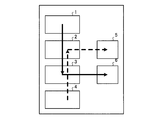
- FIG. 1 is a diagram showing a schematic functional configuration of a power conversion device according to an embodiment of the present invention.
- FIG. 2 is a diagram showing a detailed configuration of each switching element in the leg for one phase shown in FIG.
- FIG. 3 is a schematic diagram schematically showing the arrangement of four switching elements and two clamp diodes arranged on an element substrate on which one cooler is mounted.
- FIG. 4 is a diagram showing a state of temperature rise in the case of operation pattern 1 (for example, regenerative operation).
- FIG. 5 is a diagram showing a state of temperature rise in the case of operation pattern 2 (for example, power running operation).
- FIG. 6 is a diagram for explaining an arrangement position of the external element temperature sensor.
- FIG. 7 is a diagram for explaining an arrangement position of the temperature sensor for the inner element.
- FIG. 1 is a diagram showing a schematic functional configuration of a power conversion device according to an embodiment of the present invention.
- FIG. 2 is a diagram showing a detailed configuration of each switching element in the leg for one
- FIG. 8 is a diagram illustrating an example of a wiring region on the element substrate.
- FIG. 9 is a diagram showing a main circuit inductance loop in a specific switching mode.
- FIG. 10 is a diagram showing a main circuit inductance loop different from FIG. 9 in a specific switching mode.
- FIG. 11 is a diagram showing a main circuit inductance loop different from those in FIGS. 9 and 10 in a specific switching mode.
- FIG. 12 is a diagram showing a main circuit inductance loop different from those of FIGS. 9, 10 and 11 in a specific switching mode.
- FIG. 13 is a diagram showing first and second inductance loops on the chip layout diagram according to the present embodiment.
- FIG. 14 is a diagram showing the third and fourth inductance loops on the chip layout according to the present embodiment.
- FIG. 15 is a diagram showing first and second inductance loops on a chip layout diagram shown as a comparative example.
- FIG. 16 is a diagram showing third and fourth inductance loop
- FIG. 1 is a diagram showing a schematic functional configuration of a power conversion device according to an embodiment of the present invention, and shows a configuration example of a power conversion device 90 mounted on a railway vehicle 100.
- the power conversion device 90 includes a converter circuit 70, a DC voltage circuit 75 having a neutral point, and an inverter circuit 80.
- the DC voltage circuit 75 has capacitors 7 and 8 connected in series, and three potential ends are formed by one end of each of the capacitors 7 and 8 and a connection point of the capacitors 7 and 8. 70 and the inverter circuit 80 operate as a three-level power converter.
- the railroad vehicle 100 includes a transformer 65 disposed on the input end side of the power conversion device 90 and connected to the converter circuit 70, and disposed on the output end side of the power conversion device 90 and connected to the inverter circuit 80.
- An electric motor 66 that receives power supplied from the converter 90 and drives the vehicle is mounted.
- an induction motor or a synchronous motor is suitable as the electric motor 66.
- One end of the primary winding of the transformer 65 is connected to the overhead wire 61 via the current collector 62, and the other end is connected to the rail 64 that is a ground potential via the wheel 63.
- the power supplied from the overhead wire 61 is input to the primary winding of the transformer 65 through the current collector 62, and the power generated in the secondary winding of the transformer 65 is input to the converter circuit 70.
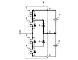
- Converter circuit 70 includes a U-phase positive arm composed of switching elements 11 and 12 and clamp diode 15, a U-phase negative arm composed of switching elements 13 and 14 and clamp diode 16, switching elements 21 and 22 and clamp.
- a V-phase positive arm composed of the diode 25 and a V-phase negative arm composed of the switching elements 23 and 24 and the clamp diode 26 are configured.
- the switching elements 11, 12, 13, and 14 are connected in series in this order, and the interconnection point of the switching elements 12 and 13 is connected to one end of the transformer 65.
- the cathode end of the clamp diode 15 is connected to the interconnection point of the switching elements 11 and 12, and the anode end of the clamp diode 15 is the connection point of the capacitors 7 and 8 which are the neutral points of the DC voltage circuit 75 or the connection point. Is connected to the same potential end.
- the negative arm has the same configuration, the anode end of the clamp diode 16 is connected to the interconnection point of the switching elements 13 and 14, and the cathode end is the neutral point of the DC voltage circuit 75 (the connection point of the capacitors 7 and 8 or This is an end of the same potential as the connection point and is also the anode end of the clamp diode 15).
- the U-phase positive arm composed of the switching elements 11 and 12 and the clamp diode 15 and the U-phase negative arm composed of the switching elements 13 and 14 and the clamp diode 16 are connected in series.
- a circuit part (leg) is comprised. This configuration is the same for the V-phase positive arm and the V-phase negative arm, and the converter circuit 70 includes a single-phase bridge circuit having two sets of legs (for U-phase and V-phase). .
- the converter circuit 70 performs PWM control of the switching elements 11 to 14 and the switching elements 21 to 24, thereby converting the input AC voltage into a desired DC voltage and outputting it to the DC voltage circuit 75. Note that PWM control for the converter circuit 70 is well-known, and a description thereof is omitted here.
- An inverter circuit 80 is connected to the output terminal of the DC voltage circuit 75.
- the inverter circuit 80 receives each DC voltage from the capacitors 7 and 8 and converts it into an AC voltage having an arbitrary voltage and an arbitrary frequency.
- the leg configuration of the inverter circuit 80 is the same as that of the converter circuit 70, and the difference is the number of phases of the leg. That is, the inverter circuit 80 includes a U-phase positive arm composed of the switching elements 31 and 32 and the clamp diode 35, a U-phase negative arm composed of the switching elements 33 and 34 and the clamp diode 36, and the switching elements 41 and 42. And a V-phase positive side arm composed of switching elements 51 and 52 and a clamp diode 55. The arm and the V-phase negative arm composed of the switching elements 53 and 54 and the clamp diode 56 are provided. The inverter circuit 80 is provided with three sets of legs (U-phase, V-phase, and W-phase). Having a three-phase bridge circuit.
- the inverter circuit 80 performs PWM control on the switching elements 31 to 34, the switching elements 41 to 44, and the switching elements 51 to 54, thereby converting the input DC voltage into a desired AC voltage and outputting it to the electric motor 66.
- PWM control for the inverter circuit 80 is well-known, and a description thereof is omitted here.
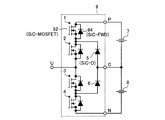
- FIG. 2 is a diagram showing a detailed configuration of each switching element in the leg for one phase shown in FIG.
- the switching element 1 includes a SiC-MOSFET 92 based on SiC and a SiC-FWD (Fly Wheel Diode) 94 based on SiC in reverse parallel as the switching elements constituting the leg 9. It is an element connected to.
- the clamp diode 5 is also a diode (SiC-D) formed of SiC. The same applies to the other switching elements 2 to 4 and the clamp diode 6.
- the four switching elements and the two clamp diodes thus configured constitute a leg for one phase.
- the leg 9 shown in FIG. 2 is also a structural unit as a power module, and the switching elements 1 to 4 and the clamp diodes 5 and 6 are housed and packaged in one module including a temperature sensor described later. .
- the terminal drawn from the connection point of the switching elements 2 and 3 forms a U terminal which is an AC terminal, and the terminal drawn from the drain end of the switching element 1 is connected to the high potential side of the DC voltage circuit.
- a P terminal (high potential side DC terminal) is formed, a terminal drawn from the source end of the switching element 4 forms an N terminal (low potential side DC terminal) connected to the low potential side of the DC voltage circuit, and is clamped Terminals drawn from the connection points of the diodes 5 and 6 form a C terminal (DC intermediate terminal) connected to the neutral point of the DC voltage circuit.
- output terminals of two temperature sensors which will be described later, are also drawn out from the module, and these terminals are combined with the terminals of the module.
- FIG. 3 is a schematic diagram schematically showing the arrangement of four switching elements and two clamp diodes arranged on an element substrate 82 on which one cooler is mounted.
- the reference numerals of the clamp diodes correspond to those shown in FIG.
- the first switching element, the first clamp diode, and the second switching element are arranged on one side of the element substrate 82 along the direction in which the cooling air flows. Are arranged in a column in this order.
- the fourth switching element, the second clamp diode, and the third switching element are arranged in tandem in this order on the other side of the element substrate 82 along the direction in which the cooling air flows.
- the switching elements 1 and 4 are disposed on the windward side with respect to the cooling air, and the switching elements 2 and 3 are disposed on the leeward side.
- these arrangement relationships may be reversed. That is, the switching elements 1 and 4 may be disposed on the leeward side of the cooling air, and the switching elements 2 and 3 may be disposed on the leeward side of the cooling air.
- FIG. 3 is characteristic in the element arrangement shown in FIG. 3, as can be understood from the comparison with FIG. 2, the circuit configuration and the element arrangement are different. Such an element arrangement will be described later.
- FIGS. 4 and 5 are diagrams showing how the temperature rises due to an operation pattern assumed when the power conversion device of the present embodiment is used for, for example, a railway vehicle.
- FIG. 4 shows operation pattern 1 (for example, regeneration).
- FIG. 5 shows a state of temperature increase in the case of operation pattern 2 (for example, power running operation).
- These element substrates 82 exemplify one of the element substrates mounted on the inverter circuit 80 among the element substrates mounted on the converter circuit 70 and the inverter circuit 80 and constituting one leg.
- the generation loss of the switching elements 1 and 4 is large and the generation loss of the switching elements 2 and 3 is small. That is, among the four switching elements constituting one leg, the switching element (hereinafter referred to as “outer element”) arranged outside the leg is the switching element (hereinafter referred to as “inner element”) arranged inside the leg. Loss) is greater than Therefore, the temperature of the portion where each switching element is mounted (hereinafter referred to as “mounting surface temperature”) is greater for the outer element than for the inner element.
- the generation loss of the switching elements 2 and 3 is large, and the generation loss of the switching elements 1 and 4 is small. That is, the reverse of the case of FIG. 4, the generated loss of the inner element is larger than that of the outer element, and the mounting surface temperature of the inner element is larger than that of the outer element.
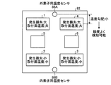
- one temperature sensor (outer element temperature sensor 86 ⁇ / b> A) is arranged in the vicinity of switching elements 1 and 4 that are outer elements.
- another temperature sensor (internal element temperature sensor 86B) is arranged in the vicinity of the switching elements 2 and 3 which are internal elements. If the temperature sensor 86A for the external element is arranged at a substantially equidistant position from the switching elements 1 and 4, the temperature gradient from the switching element 1 and the temperature gradient from the switching element 4 at the position are approximately equal. It becomes possible to accurately detect the temperatures of these switching elements 1 and 4. The same applies to the temperature sensor 86B for the inner element, and the temperature of the switching elements 2 and 3 can be accurately detected by disposing the temperature sensor 86B at approximately the same distance from the switching elements 2 and 3.
- a simple heat dissipation mechanism such as a heat sink using a three-level power conversion device for a railway vehicle, using a SiC semiconductor as each switching element.
- the operation of each switching element differs depending on the operation mode unique to the railway vehicle, and the temperature gradient on the element substrate as viewed from the entire element substrate increases.
- the temperature rise of the switching elements 1 and 4 (that is, the external elements) having a large generation loss and a high mounting surface temperature is caused by the external element temperature sensor 86A. It can be detected with high accuracy. This is because the external element temperature sensor 86A is disposed in the vicinity of the switching elements 1 and 4, and thus the temperature gradient between the external element temperature sensor 86A and the switching elements 1 and 4 is small.
- the temperature rise of the switching elements 2 and 3 (that is, the inner element) having a large generation loss and a high mounting surface temperature is caused by the inner element temperature sensor 86B. It can be detected with high accuracy. Since the internal element temperature sensor 86B is disposed in the vicinity of the switching elements 2 and 3, the temperature gradient between the internal element temperature sensor 86B and the switching elements 2 and 3 is small. Therefore, it is possible to accurately detect the temperature rise of the switching elements 2 and 3.
- the over-temperature control by the outer element temperature sensor 86A and the inner element temperature sensor 86B may be, for example, processing using the logical sum output of both. That is, when at least one of the outer element temperature sensor 86A and the inner element temperature sensor 86B detects an overtemperature, the overtemperature control of the entire module may be performed.
- the outer element temperature sensor 86A and the inner element temperature sensor 86B will be described.
- Some temperature sensors such as a temperature relay, detect that a set value has been reached and open and close the contacts, while others, such as a thermistor, can detect the temperature itself.
- the temperature sensor assumed in the present embodiment is the former type.
- the set values set in the outer element temperature sensor 86A and the inner element temperature sensor 86B are set in consideration of a temperature gradient generated between the switching element to be detected and the sensor position. However, in the power conversion device of the present embodiment, each temperature sensor is disposed at a position where the temperature gradient generated between the switching element to be detected becomes small, and thus operates at a temperature deviating from a desired temperature value. The probability is very low.
- the set values of the outer element temperature sensor 86A and the inner element temperature sensor 86B do not have to be the same, but are generally different. These set values may be determined in consideration of the strength of the cooling air, the direction of the cooling air, the temperature rise pattern of the switching element according to the operation mode of the power converter. In this sense, any one of the switching elements 1 and 4 or the switching elements 2 and 3 may be located on the cooling wind.
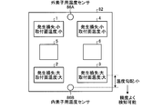
- FIG. 8 is a diagram illustrating an example of a wiring area on the element substrate 82.
- the temperature sensor 86A for the external element is arranged on the side of the element substrate 82 in the vicinity of the periphery of the external element (switching elements 1 and 4) is for this reason. is there.
- the temperature sensor 86B for the inner element is arranged on the side of the element substrate 82 in the vicinity region around the inner elements (switching elements 2 and 3).
- the region on the left side (side portion side) of the clamp diode 5 and the region on the right side (side portion side) of the clamp diode 6 are not included in the wiring region. It is also possible to arrange a sensor. However, the operation modes of the power conversion device shown in FIGS. 4 and 5 are not preferable because the mounting surface temperatures of the switching element 1 and the switching element 2 are different. For example, when a temperature sensor is arranged at a position approximately equidistant from the switching element 1 and the switching element 2 (region on the left side of the clamp diode 5), the temperature in the vicinity of the average value of both is detected. It is difficult to accurately estimate the mounting surface temperature. However, when the mounting surface temperatures of the switching element 1 and the switching element 2 are increased / decreased at the same time, this area is rather a preferable area for arranging the temperature sensor.
- FIG. 9 to 12 are diagrams for explaining the influence of the main circuit inductance, and show the main circuit inductance loop in the three-level inverter.
- FIG. 9 shows a first inductance loop passing through the switching element 1 and the clamp diode 5.
- FIG. 10 shows a second inductance loop that passes through the switching element 1, the switching element 2, the switching element 3, and the clamp diode 6, and
- FIG. 11 shows a third inductance loop that passes through the switching element 4 and the clamp diode 6.
- FIG. 12 shows a fourth inductance loop that passes through the switching element 4, the switching element 3, the switching element 2, and the clamp diode 5. Note that these first to fourth inductance loops indicate a path of back electromotive force (L ⁇ di / dt) in a specific switching mode, and do not indicate a current path in a specific switching mode. .
- FIG. 13 is a diagram showing the first and second inductance loops on the chip layout according to the present embodiment.
- an arrow indicated by a thick solid line is a path between chips related to the first inductance loop
- an arrow indicated by a thick broken line is a path between chips related to the second inductance loop. Since the inductance component in each inductance loop is proportional to the loop length, it can be seen that the L component in the first and second inductance loops is set to a minimum value between the chips.
- FIG. 14 is a diagram showing the third and fourth inductance loops on the chip layout according to the present embodiment.
- an arrow indicated by a thick solid line is a path between chips related to the third inductance loop
- an arrow indicated by a thick broken line is a path between chips related to the fourth inductance loop.
- the loop length between chips in this loop is longer than the loop length between chips in the first inductance loop shown in FIG.
- the portions indicated by “ ⁇ ” symbols are portions that are turned back, and the inductance components of these portions are cancelled.
- the inductance component in the third inductance loop is substantially only the portion indicated by the “ ⁇ ” symbol, and the L component in the third inductance loop is set to be as small as possible. I understand. This effect is the same in the fourth inductance loop, and it can be seen that the L component in the fourth inductance loop is also set to be as small as possible.
- 15 and 16 are chip layout diagrams shown as comparative examples.
- the four switching elements and two clamp diodes constituting one leg are visually identical to the circuit diagram shown in FIG. 2 and the like. It is arranged to be.
- an arrow indicated by a thick solid line is a path between chips related to the first inductance loop
- an arrow indicated by a thick broken line is a path between chips related to the second inductance loop.
- an arrow indicated by a thick solid line is a path between chips related to the third inductance loop
- an arrow indicated by a thick broken line is a path between chips related to the fourth inductance loop.
- switching elements 1 to 4 and clamp diodes 5 and 6 are formed of a wide band gap semiconductor, and switching element 1, clamp diode 5 and switching element 2 are cooled.
- the switching element 4, the clamp diode 6 and the switching element 3 are arranged in this order on one side of the element substrate 82 along the flow direction of the wind, and are arranged on the other side of the element substrate 82 along the direction of the cooling air flow.
- the outer element temperature sensor 86A is arranged on the side of the element substrate 82 in the vicinity of the switching elements 1 and 4 and the inner element temperature sensor 86B is in the vicinity of the vicinity of the switching elements 2 and 3.
- the switching elements 1 to 4 Since the amplifier diodes 5 and 6, the outer element temperature sensor 86A and the inner element temperature sensor 86B are housed in one module, it is suitable for use in a three-level power conversion device with a simplified cooler. The effect that a semiconductor module can be obtained is obtained.
- FIG. 4 and 5 are diagrams showing a temperature rise in the one-leg element substrate 82 mounted on the inverter circuit 80.
- the temperature increase in the element substrate 82 mounted on the converter circuit 70 is as follows. The pattern is the reverse of that of the inverter circuit 80. That is, if the temperature rise on the element substrate 82 mounted on the inverter circuit 80 is in the state shown in FIG. 4, the temperature rise on the element substrate 82 mounted on the converter circuit 70 is in the state shown in FIG. On the contrary, if the temperature rise on the element substrate 82 mounted on the inverter circuit 80 is in the state shown in FIG. 5, the temperature rise on the element substrate 82 mounted on the converter circuit 70 is the state shown in FIG. It becomes. Therefore, the method according to the present embodiment can be applied without distinguishing between the inverter circuit and the converter circuit.
- the SiC-MOSFET is used as the switching element, and the SiC-FWD is used as the diode (FWD) connected in reverse parallel to the switching element.
- the effect that the chip size can be reduced can be obtained.
- SiC-FWD since the on-voltage can be reduced, the effect that the recovery loss can be greatly reduced is also obtained. Note that, for example, if a SiC-based Schottky barrier diode (SiC-SBD) is used as the FWD, an effect that recovery loss can be further reduced can be obtained.
- SiC-SBD SiC-based Schottky barrier diode
- the SiC semiconductor is an example of a semiconductor referred to as a wide band gap semiconductor.
- a semiconductor formed using, for example, a gallium nitride material or diamond belongs to the wide band gap semiconductor. Therefore, a configuration using a wide bandgap semiconductor other than the SiC semiconductor also forms the gist of the present invention.
- the description of the invention is carried out for a power semiconductor module that is assumed to be applied to a railway vehicle.
- the application field is not limited to this, and various industrial application fields are applied. Needless to say, this is applicable.
- the power semiconductor module according to the present invention is useful for a three-level power conversion device with a simplified cooler.
Landscapes
- Engineering & Computer Science (AREA)
- Power Engineering (AREA)
- Transportation (AREA)
- Mechanical Engineering (AREA)
- Microelectronics & Electronic Packaging (AREA)
- Life Sciences & Earth Sciences (AREA)
- Sustainable Development (AREA)
- Sustainable Energy (AREA)
- Physics & Mathematics (AREA)
- Thermal Sciences (AREA)
- Inverter Devices (AREA)
- Electric Propulsion And Braking For Vehicles (AREA)
Abstract
Description
5,6,15,16,25,26,35,36,45,46,55,56 クランプダイオード
7,8 コンデンサ
9 レグ
61 架線
62 集電装置
63 車輪
64 レール
65 変圧器
66 電動機
70 コンバータ回路
75 直流電圧回路
80 インバータ回路
82 素子基板
84 配線領域
86A 外素子用温度センサ
86B 内素子用温度センサ
90 電力変換装置
100 鉄道車両
Claims (5)
- 鉄道車両用の3レベル電力変換装置に適用されるパワー半導体モジュールにおいて、
高電位側直流端子と交流端子との間にこの順序で直列に接続され、オンオフ制御されて動作する第1、第2のスイッチング素子と、
前記交流端子と低電位側直流端子との間にこの順序で直列に接続され、オンオフ制御されて動作する第3、第4のスイッチング素子と、
カソード端子が前記第1、第2のスイッチング素子の相互接続点に接続され、アノード端子が直流中間端子に接続される第1のクランプダイオードと、
カソード端子が前記直流中間端子に接続され、アノード端子が前記第1、第2のスイッチング素子の相互接続点に接続される第2のクランプダイオードと、
前記第1および第2のスイッチング素子の過温度検知を行う第1の温度リレーと、
前記第3および第4のスイッチング素子の過温度検知を行う第2の温度リレーと、
を有し、
前記第1~第4のスイッチング素子および前記第1、第2のクランプダイオードは、ワイドバンドギャップ半導体により形成され、
前記第1のスイッチング素子、前記第1のクランプダイオードおよび前記第2のスイッチング素子は、冷却風の流れる方向に沿って素子基板の一方側に、この順序で縦列に配置され、
前記第4のスイッチング素子、前記第2のクランプダイオードおよび前記第3のスイッチング素子は、前記冷却風の流れる方向に沿って前記素子基板の他方側に、この順序で縦列に配置され、
前記第1の温度リレーは、前記第1、第4のスイッチング素子周辺の近傍領域における前記素子基板の辺部側に配置され、
前記第2の温度リレーは、前記第2、第3のスイッチング素子周辺の近傍領域における前記素子基板の辺部側に配置され、
前記第1~第4のスイッチング素子、前記第1、第2のクランプダイオードおよび前記第1、第2の温度リレーは、1つのモジュール内に収容されて構成されていることを特徴とするパワー半導体モジュール。 - 前記第1の温度リレーは、前記第1のスイッチング素子と前記第4のスイッチング素子とから概略等距離の位置に配置され、
前記第2の温度リレーは、前記第2のスイッチング素子と前記第3のスイッチング素子とから概略等距離の位置に配置されている
ことを特徴とする請求項1に記載のパワー半導体モジュール。 - 前記ワイドバンドギャップ半導体は、炭化ケイ素、窒化ガリウム系材料または、ダイヤモンドを用いた半導体であることを特徴とする請求項1または2に記載のパワー半導体モジュール。
- 高電位側直流端子と交流端子との間にこの順序で直列に接続され、オンオフ制御されて動作する第1、第2のスイッチング素子と、
前記交流出力端子と低電位側直流端子との間にこの順序で直列に接続され、オンオフ制御されて動作する第3、第4のスイッチング素子と、
カソード端子が前記第1、第2のスイッチング素子の相互接続点に接続され、アノード端子が直流中間端子に接続される第1のクランプダイオードと、
カソード端子が前記直流中間端子に接続され、アノード端子が前記第1、第2のスイッチング素子の相互接続点に接続される第2のクランプダイオードと、
前記第1および第2のスイッチング素子の過温度検知を行う第1の温度リレーと、
前記第3および第4のスイッチング素子の過温度検知を行う第2の温度リレーと、
を具備するレグを複数組有し、
前記第1~第4のスイッチング素子および前記第1、第2のクランプダイオードは、ワイドバンドギャップ半導体により形成され、
前記第1のスイッチング素子、前記第1のクランプダイオードおよび前記第2のスイッチング素子は、冷却風の流れる方向に沿って素子基板の一方側に、この順序で縦列に配置され、
前記第4のスイッチング素子、前記第2のクランプダイオードおよび前記第3のスイッチング素子は、前記冷却風の流れる方向に沿って前記素子基板の他方側に、この順序で縦列に配置され、
前記第1の温度リレーは、前記第1、第4のスイッチング素子周辺の近傍領域における前記素子基板の辺部側に配置され、
前記第2の温度リレーは、前記第2、第3のスイッチング素子周辺の近傍領域における前記素子基板の辺部側に配置され、
前記第1~第4のスイッチング素子、前記第1、第2のクランプダイオードおよび前記第1、第2の温度リレーは、前記レグ毎に1つのモジュール内に収容されて構成されていることを特徴とする電力変換装置。 - 入力された直流電圧または交流電圧を所望の交流電圧に変換して出力する電力変換装置と、前記電力変換装置からの電力供給を受けて車両を駆動する電動機と、を備えた鉄道車両において、
前記電力変換装置は、
高電位側直流端子と交流端子との間にこの順序で直列に接続され、オンオフ制御されて動作する第1、第2のスイッチング素子と、
前記交流出力端子と低電位側直流端子との間にこの順序で直列に接続され、オンオフ制御されて動作する第3、第4のスイッチング素子と、
カソード端子が前記第1、第2のスイッチング素子の相互接続点に接続され、アノード端子が直流中間端子に接続される第1のクランプダイオードと、
カソード端子が前記直流中間端子に接続され、アノード端子が前記第1、第2のスイッチング素子の相互接続点に接続される第2のクランプダイオードと、
前記第1および第2のスイッチング素子の過温度検知を行う第1の温度リレーと、
前記第3および第4のスイッチング素子の過温度検知を行う第2の温度リレーと、
を具備するレグを複数組有し、
前記第1~第4のスイッチング素子および前記第1、第2のクランプダイオードは、ワイドバンドギャップ半導体により形成され、
前記第1のスイッチング素子、前記第1のクランプダイオードおよび前記第2のスイッチング素子は、冷却風の流れる方向に沿って素子基板の一方側に、この順序で縦列に配置され、
前記第4のスイッチング素子、前記第2のクランプダイオードおよび前記第3のスイッチング素子は、前記冷却風の流れる方向に沿って前記素子基板の他方側に、この順序で縦列に配置され、
前記第1の温度リレーは、前記第1、第4のスイッチング素子周辺の近傍領域における前記素子基板の辺部側に配置され、
前記第2の温度リレーは、前記第2、第3のスイッチング素子周辺の近傍領域における前記素子基板の辺部側に配置され、
前記第1~第4のスイッチング素子、前記第1、第2のクランプダイオードおよび前記第1、第2の温度リレーは、前記レグ毎に1つのモジュール内に収容されて構成されていることを特徴とする鉄道車両。
Priority Applications (6)
| Application Number | Priority Date | Filing Date | Title |
|---|---|---|---|
| PCT/JP2010/065561 WO2012032642A1 (ja) | 2010-09-09 | 2010-09-09 | パワー半導体モジュール、電力変換装置および鉄道車両 |
| EP10856989.8A EP2615733A4 (en) | 2010-09-09 | 2010-09-09 | SEMICONDUCTOR CURRENT MODULE, CURRENT CONVERSION DEVICE AND RAIL VEHICLE |
| US13/821,417 US20130169035A1 (en) | 2010-09-09 | 2010-09-09 | Power semiconductor module, power conversion apparatus, and railroad vehicle |
| CN201080068993.6A CN103081332B (zh) | 2010-09-09 | 2010-09-09 | 功率半导体模块、电力转换装置及铁路车辆 |
| JP2011526742A JP4869454B1 (ja) | 2010-09-09 | 2010-09-09 | パワー半導体モジュール、電力変換装置および鉄道車両 |
| BR112013005702A BR112013005702A2 (pt) | 2010-09-09 | 2010-09-09 | módulo de semicondutor de potência, aparelho de conversão de potência, veículo ferroviário |
Applications Claiming Priority (1)
| Application Number | Priority Date | Filing Date | Title |
|---|---|---|---|
| PCT/JP2010/065561 WO2012032642A1 (ja) | 2010-09-09 | 2010-09-09 | パワー半導体モジュール、電力変換装置および鉄道車両 |
Publications (1)
| Publication Number | Publication Date |
|---|---|
| WO2012032642A1 true WO2012032642A1 (ja) | 2012-03-15 |
Family
ID=45781896
Family Applications (1)
| Application Number | Title | Priority Date | Filing Date |
|---|---|---|---|
| PCT/JP2010/065561 Ceased WO2012032642A1 (ja) | 2010-09-09 | 2010-09-09 | パワー半導体モジュール、電力変換装置および鉄道車両 |
Country Status (6)
| Country | Link |
|---|---|
| US (1) | US20130169035A1 (ja) |
| EP (1) | EP2615733A4 (ja) |
| JP (1) | JP4869454B1 (ja) |
| CN (1) | CN103081332B (ja) |
| BR (1) | BR112013005702A2 (ja) |
| WO (1) | WO2012032642A1 (ja) |
Cited By (14)
| Publication number | Priority date | Publication date | Assignee | Title |
|---|---|---|---|---|
| CN102739069A (zh) * | 2012-06-18 | 2012-10-17 | 深圳市英威腾电气股份有限公司 | 一种功率半导体模块以及应用其的电力电子设备 |
| JP2013090427A (ja) * | 2011-10-18 | 2013-05-13 | Hitachi Ltd | 電力変換装置 |
| CN103107724A (zh) * | 2013-01-29 | 2013-05-15 | 上海电气集团股份有限公司 | 一种三电平变流器的模块化结构 |
| JP2013230010A (ja) * | 2012-04-26 | 2013-11-07 | Hitachi Ltd | 電力変換装置 |
| JP2014014203A (ja) * | 2012-07-03 | 2014-01-23 | Mitsubishi Electric Corp | 電力変換装置 |
| CN103973131A (zh) * | 2013-02-06 | 2014-08-06 | 富士电机株式会社 | 半导体系统 |
| CN104838576A (zh) * | 2013-02-06 | 2015-08-12 | 富士电机株式会社 | 半导体装置 |
| WO2016157532A1 (ja) * | 2015-04-03 | 2016-10-06 | 株式会社 東芝 | 電力変換装置 |
| WO2016157533A1 (ja) * | 2015-04-03 | 2016-10-06 | 株式会社 東芝 | 電力変換装置 |
| JP2017112690A (ja) * | 2015-12-15 | 2017-06-22 | 株式会社東芝 | 電力変換装置 |
| JP2017184387A (ja) * | 2016-03-29 | 2017-10-05 | 東芝三菱電機産業システム株式会社 | セルインバータユニット |
| JP2019092302A (ja) * | 2017-11-15 | 2019-06-13 | 富士電機株式会社 | 電力変換装置および鉄道車両用電力変換装置 |
| WO2020250486A1 (ja) * | 2019-06-14 | 2020-12-17 | 株式会社日立製作所 | 電力変換装置 |
| JPWO2020137133A1 (ja) * | 2018-12-26 | 2021-10-14 | 株式会社日立製作所 | 鉄道車両用の電力変換装置 |
Families Citing this family (19)
| Publication number | Priority date | Publication date | Assignee | Title |
|---|---|---|---|---|
| CN103354973B (zh) * | 2011-01-31 | 2016-08-10 | 三菱电机株式会社 | 功率转换装置 |
| CN103138595B (zh) * | 2011-11-22 | 2016-05-25 | 通用电气公司 | 中点箝位式变流器的控制系统及控制方法 |
| US20140119088A1 (en) * | 2012-10-29 | 2014-05-01 | Huawei Technologies Co., Ltd. | Three-level inverter and power supply equipment |
| CN104038085B (zh) * | 2013-03-08 | 2016-07-06 | 台达电子工业股份有限公司 | 三电平变流器 |
| JP2015050257A (ja) * | 2013-08-30 | 2015-03-16 | 株式会社東芝 | 車両用電力変換装置及び鉄道車両 |
| EP3084952A4 (en) * | 2013-12-18 | 2017-10-11 | Otis Elevator Company | Bus capacitor bank configuration for a multi-level regenerative drive |
| CN104270014A (zh) * | 2014-07-31 | 2015-01-07 | 深圳市英威腾电气股份有限公司 | 一种三电平大功率模组结构及功率变换装置 |
| US9954409B2 (en) * | 2015-07-27 | 2018-04-24 | Ford Global Technologies, Llc | Power supply device |
| US10858911B2 (en) | 2015-09-04 | 2020-12-08 | Baker Hughes, A Ge Company, Llc | Bidirectional chopping of high voltage power in high temperature downhole tools to reduce tool size |
| JP6395166B1 (ja) * | 2017-07-10 | 2018-09-26 | 三菱電機株式会社 | 電力変換装置 |
| US10461651B2 (en) * | 2017-12-05 | 2019-10-29 | Abb Schweiz Ag | Soft-switching power converters using air-core resonant inductor |
| CN110581534B (zh) * | 2018-06-11 | 2021-08-03 | 台达电子工业股份有限公司 | 温度保护电路 |
| WO2020025376A1 (de) * | 2018-07-31 | 2020-02-06 | Siemens Aktiengesellschaft | Modularer stromrichter |
| US10651761B2 (en) * | 2018-09-14 | 2020-05-12 | Hamilton Sundstrand Corporation | Power converters with segregated switch and drive modules |
| CN114342209A (zh) | 2019-09-13 | 2022-04-12 | 米沃奇电动工具公司 | 具有宽带隙半导体的功率转换器 |
| DE102019214719A1 (de) * | 2019-09-26 | 2021-04-01 | Bombardier Transportation Gmbh | Stromrichter, elektrisches Antriebssystem und Verfahren zum Betrieb eines Stromrichters |
| CN113381583B (zh) * | 2020-03-09 | 2024-05-31 | 株洲中车时代电气股份有限公司 | 一种牵引变流装置 |
| JP7547987B2 (ja) * | 2020-12-18 | 2024-09-10 | 株式会社村田製作所 | 電力増幅器 |
| CN113783436B (zh) * | 2021-09-27 | 2023-10-20 | 广东电网有限责任公司阳江供电局 | 一种全功率风电变换器及控制方法 |
Citations (5)
| Publication number | Priority date | Publication date | Assignee | Title |
|---|---|---|---|---|
| JPH10210759A (ja) | 1997-01-17 | 1998-08-07 | Toyo Electric Mfg Co Ltd | 3レベルインバータ装置 |
| JPH1189249A (ja) * | 1997-09-08 | 1999-03-30 | Mitsubishi Electric Corp | 3レベル電力変換装置 |
| JP2003134823A (ja) * | 2001-10-16 | 2003-05-09 | Hitachi Ltd | 電力変換装置 |
| JP2005287267A (ja) * | 2004-03-31 | 2005-10-13 | Mitsubishi Electric Corp | 電力変換装置 |
| JP2010098820A (ja) * | 2008-10-15 | 2010-04-30 | Toshiba Corp | 電力変換装置 |
Family Cites Families (9)
| Publication number | Priority date | Publication date | Assignee | Title |
|---|---|---|---|---|
| US6747884B2 (en) * | 2001-04-13 | 2004-06-08 | Mitsubishi Denki Kabushiki Kaisha | Power converter device |
| TW200530566A (en) * | 2004-03-05 | 2005-09-16 | Hitachi Ind Equipment Sys | Method for detecting temperature of semiconductor element and semiconductor power converter |
| JP4600159B2 (ja) * | 2005-06-01 | 2010-12-15 | 三菱電機株式会社 | 3レベル電力変換装置 |
| WO2009150889A1 (ja) * | 2008-06-11 | 2009-12-17 | シャープ株式会社 | 液晶温度センサー、液晶温度センサーの温度検出方法、液晶装置及び液晶装置の駆動方法 |
| CA2742809C (en) * | 2008-11-11 | 2014-09-09 | Pv Powered, Inc. | Solar power inverters, including temperature-controlled solar power inverters, and associated systems and methods |
| WO2010073635A1 (ja) * | 2008-12-26 | 2010-07-01 | ダイキン工業株式会社 | 電力変換装置 |
| KR101410553B1 (ko) * | 2010-07-01 | 2014-06-20 | 미쓰비시덴키 가부시키가이샤 | 파워 반도체 모듈, 전력 변환 장치, 및 철도 차량 |
| DK2456059T3 (en) * | 2010-11-17 | 2018-08-27 | Abb Schweiz Ag | Switch branch module for a three level converter and method for controlling this switch branch |
| JP5663450B2 (ja) * | 2011-10-18 | 2015-02-04 | 株式会社日立製作所 | 電力変換装置 |
-
2010
- 2010-09-09 CN CN201080068993.6A patent/CN103081332B/zh not_active Expired - Fee Related
- 2010-09-09 JP JP2011526742A patent/JP4869454B1/ja not_active Expired - Fee Related
- 2010-09-09 WO PCT/JP2010/065561 patent/WO2012032642A1/ja not_active Ceased
- 2010-09-09 BR BR112013005702A patent/BR112013005702A2/pt not_active IP Right Cessation
- 2010-09-09 EP EP10856989.8A patent/EP2615733A4/en not_active Withdrawn
- 2010-09-09 US US13/821,417 patent/US20130169035A1/en not_active Abandoned
Patent Citations (5)
| Publication number | Priority date | Publication date | Assignee | Title |
|---|---|---|---|---|
| JPH10210759A (ja) | 1997-01-17 | 1998-08-07 | Toyo Electric Mfg Co Ltd | 3レベルインバータ装置 |
| JPH1189249A (ja) * | 1997-09-08 | 1999-03-30 | Mitsubishi Electric Corp | 3レベル電力変換装置 |
| JP2003134823A (ja) * | 2001-10-16 | 2003-05-09 | Hitachi Ltd | 電力変換装置 |
| JP2005287267A (ja) * | 2004-03-31 | 2005-10-13 | Mitsubishi Electric Corp | 電力変換装置 |
| JP2010098820A (ja) * | 2008-10-15 | 2010-04-30 | Toshiba Corp | 電力変換装置 |
Non-Patent Citations (1)
| Title |
|---|
| See also references of EP2615733A4 * |
Cited By (18)
| Publication number | Priority date | Publication date | Assignee | Title |
|---|---|---|---|---|
| JP2013090427A (ja) * | 2011-10-18 | 2013-05-13 | Hitachi Ltd | 電力変換装置 |
| JP2013230010A (ja) * | 2012-04-26 | 2013-11-07 | Hitachi Ltd | 電力変換装置 |
| CN102739069A (zh) * | 2012-06-18 | 2012-10-17 | 深圳市英威腾电气股份有限公司 | 一种功率半导体模块以及应用其的电力电子设备 |
| JP2014014203A (ja) * | 2012-07-03 | 2014-01-23 | Mitsubishi Electric Corp | 電力変換装置 |
| CN103107724A (zh) * | 2013-01-29 | 2013-05-15 | 上海电气集团股份有限公司 | 一种三电平变流器的模块化结构 |
| CN104838576B (zh) * | 2013-02-06 | 2018-02-23 | 富士电机株式会社 | 半导体装置 |
| JP2014155287A (ja) * | 2013-02-06 | 2014-08-25 | Fuji Electric Co Ltd | 半導体装置 |
| CN104838576A (zh) * | 2013-02-06 | 2015-08-12 | 富士电机株式会社 | 半导体装置 |
| CN103973131A (zh) * | 2013-02-06 | 2014-08-06 | 富士电机株式会社 | 半导体系统 |
| EP2765602B1 (en) * | 2013-02-06 | 2020-09-16 | Fuji Electric Co., Ltd. | Semiconductor system |
| WO2016157532A1 (ja) * | 2015-04-03 | 2016-10-06 | 株式会社 東芝 | 電力変換装置 |
| WO2016157533A1 (ja) * | 2015-04-03 | 2016-10-06 | 株式会社 東芝 | 電力変換装置 |
| JP2017112690A (ja) * | 2015-12-15 | 2017-06-22 | 株式会社東芝 | 電力変換装置 |
| JP2017184387A (ja) * | 2016-03-29 | 2017-10-05 | 東芝三菱電機産業システム株式会社 | セルインバータユニット |
| JP2019092302A (ja) * | 2017-11-15 | 2019-06-13 | 富士電機株式会社 | 電力変換装置および鉄道車両用電力変換装置 |
| JPWO2020137133A1 (ja) * | 2018-12-26 | 2021-10-14 | 株式会社日立製作所 | 鉄道車両用の電力変換装置 |
| JP7072675B2 (ja) | 2018-12-26 | 2022-05-20 | 株式会社日立製作所 | 鉄道車両用の電力変換装置 |
| WO2020250486A1 (ja) * | 2019-06-14 | 2020-12-17 | 株式会社日立製作所 | 電力変換装置 |
Also Published As
| Publication number | Publication date |
|---|---|
| US20130169035A1 (en) | 2013-07-04 |
| JP4869454B1 (ja) | 2012-02-08 |
| BR112013005702A2 (pt) | 2016-05-03 |
| EP2615733A1 (en) | 2013-07-17 |
| CN103081332A (zh) | 2013-05-01 |
| CN103081332B (zh) | 2016-06-01 |
| JPWO2012032642A1 (ja) | 2013-12-12 |
| EP2615733A4 (en) | 2014-04-09 |
Similar Documents
| Publication | Publication Date | Title |
|---|---|---|
| JP4869454B1 (ja) | パワー半導体モジュール、電力変換装置および鉄道車両 | |
| JP5970983B2 (ja) | 電力変換装置 | |
| CN102781712B (zh) | 功率半导体模块、电力转换装置及铁路车辆 | |
| JP4722229B1 (ja) | パワー半導体モジュール、電力変換装置および鉄道車両 | |
| CN107148738B (zh) | 电力变换装置 | |
| JP5822773B2 (ja) | 電力変換装置 | |
| JP6329944B2 (ja) | 絶縁ゲート型半導体素子の制御装置およびそれを用いた電力変換装置 | |
| JP6067136B2 (ja) | 電力変換装置 | |
| US11267351B2 (en) | Power conversion device | |
| JP5851267B2 (ja) | インバータ及び車両制御装置 | |
| JP5933873B1 (ja) | 回生コンバータ | |
| JP5546664B2 (ja) | パワー半導体モジュール、電力変換装置および鉄道車両 | |
| JP5264863B2 (ja) | パワー半導体モジュール、電力変換装置および鉄道車両 | |
| JP6778160B2 (ja) | 電力変換装置及び電力変換方法 | |
| She et al. | Performance evaluation of 1.5 kV solar inverter with 2.5 kV silicon carbide MOSFET | |
| JP6007578B2 (ja) | パワー半導体モジュールおよびその組立方法 | |
| JP6690777B2 (ja) | 主変換回路、電力変換装置及び移動体 | |
| Mookken | SiC MOSFETs enable high frequency in high power conversion systems | |
| JP2020014295A (ja) | 電力変換装置及び電力変換装置における電流制御方法 | |
| JP4808290B1 (ja) | パワー半導体モジュール、電力変換装置および鉄道車両 | |
| JP2012055101A (ja) | 半導体スイッチング装置 |
Legal Events
| Date | Code | Title | Description |
|---|---|---|---|
| WWE | Wipo information: entry into national phase |
Ref document number: 201080068993.6 Country of ref document: CN |
|
| WWE | Wipo information: entry into national phase |
Ref document number: 2011526742 Country of ref document: JP |
|
| 121 | Ep: the epo has been informed by wipo that ep was designated in this application |
Ref document number: 10856989 Country of ref document: EP Kind code of ref document: A1 |
|
| WWE | Wipo information: entry into national phase |
Ref document number: 13821417 Country of ref document: US |
|
| NENP | Non-entry into the national phase |
Ref country code: DE |
|
| WWE | Wipo information: entry into national phase |
Ref document number: 2010856989 Country of ref document: EP |
|
| REG | Reference to national code |
Ref country code: BR Ref legal event code: B01A Ref document number: 112013005702 Country of ref document: BR |
|
| ENP | Entry into the national phase |
Ref document number: 112013005702 Country of ref document: BR Kind code of ref document: A2 Effective date: 20130308 |