WO2012039403A1 - 半導体装置の製造方法 - Google Patents
半導体装置の製造方法 Download PDFInfo
- Publication number
- WO2012039403A1 WO2012039403A1 PCT/JP2011/071408 JP2011071408W WO2012039403A1 WO 2012039403 A1 WO2012039403 A1 WO 2012039403A1 JP 2011071408 W JP2011071408 W JP 2011071408W WO 2012039403 A1 WO2012039403 A1 WO 2012039403A1
- Authority
- WO
- WIPO (PCT)
- Prior art keywords
- chip
- semiconductor wafer
- polyimide
- forming
- wafer
- Prior art date
- Legal status (The legal status is an assumption and is not a legal conclusion. Google has not performed a legal analysis and makes no representation as to the accuracy of the status listed.)
- Ceased
Links
Images




Classifications
-
- H—ELECTRICITY
- H10—SEMICONDUCTOR DEVICES; ELECTRIC SOLID-STATE DEVICES NOT OTHERWISE PROVIDED FOR
- H10P—GENERIC PROCESSES OR APPARATUS FOR THE MANUFACTURE OR TREATMENT OF DEVICES COVERED BY CLASS H10
- H10P58/00—Singulating wafers or substrates into multiple chips, i.e. dicing
-
- H—ELECTRICITY
- H10—SEMICONDUCTOR DEVICES; ELECTRIC SOLID-STATE DEVICES NOT OTHERWISE PROVIDED FOR
- H10D—INORGANIC ELECTRIC SEMICONDUCTOR DEVICES
- H10D12/00—Bipolar devices controlled by the field effect, e.g. insulated-gate bipolar transistors [IGBT]
- H10D12/01—Manufacture or treatment
- H10D12/031—Manufacture or treatment of IGBTs
- H10D12/032—Manufacture or treatment of IGBTs of vertical IGBTs
- H10D12/038—Manufacture or treatment of IGBTs of vertical IGBTs having a recessed gate, e.g. trench-gate IGBTs
-
- H—ELECTRICITY
- H10—SEMICONDUCTOR DEVICES; ELECTRIC SOLID-STATE DEVICES NOT OTHERWISE PROVIDED FOR
- H10P—GENERIC PROCESSES OR APPARATUS FOR THE MANUFACTURE OR TREATMENT OF DEVICES COVERED BY CLASS H10
- H10P54/00—Cutting or separating of wafers, substrates or parts of devices
-
- H—ELECTRICITY
- H10—SEMICONDUCTOR DEVICES; ELECTRIC SOLID-STATE DEVICES NOT OTHERWISE PROVIDED FOR
- H10P—GENERIC PROCESSES OR APPARATUS FOR THE MANUFACTURE OR TREATMENT OF DEVICES COVERED BY CLASS H10
- H10P72/00—Handling or holding of wafers, substrates or devices during manufacture or treatment thereof
- H10P72/04—Apparatus for manufacture or treatment
- H10P72/0428—Apparatus for mechanical treatment or grinding or cutting
Definitions
- the present invention relates to a method for manufacturing a semiconductor device, and more particularly to a method for manufacturing a semiconductor device in which a semiconductor wafer (hereinafter simply referred to as a wafer) is manufactured by dicing with a blade.
- a semiconductor wafer hereinafter simply referred to as a wafer
- IGBTs Insulated Gate Bipolar Transistors
- MOSFETs MOS Field Effect Transistors
- diodes have been developed in order to improve their electrical characteristics.
- the thickness of the silicon substrate on which the element is formed is reduced.
- FIG. 13 is an explanatory view showing a cross-sectional structure of a main part of an FS (Field Stop) -IGBT.
- the FS-IGBT includes a p-well layer 52 disposed (laminated) on the surface layer of an n-silicon substrate 51d (referred to as a wafer 51) having a thickness of about 150 ⁇ m, and the p-well. And a trench 53 penetrating the layer 52.
- the FS-IGBT includes an n-emitter layer 54 that is a surface layer of the p-well layer 52 and is disposed in contact with the trench 53.
- a gate oxide film 55 is disposed on the inner wall of the trench 53, and a gate electrode 56 is disposed inside the trench 53 via the gate oxide film 55.
- An interlayer insulating film 57 is disposed on the gate electrode 56, and an emitter electrode 58 electrically connected to the n emitter layer 54 is disposed thereon.
- An n-FS layer 60 and a p collector layer 61 are disposed on the back side of the n silicon substrate 51d, and a collector electrode 62 that is electrically connected to the p collector layer 61 is disposed. The manufacturing process of such FS-IGBT will be described below.
- a protective tape is applied to the front side of the thick wafer, and the back side of the thick wafer is ground. Thereafter, the protective tape is peeled off, and the ground layer is wet-etched to remove the crushed layer, thereby obtaining a thin wafer 51 of about 150 ⁇ m.
- Phosphorus (P) and boron (B) are ion-implanted into the back surface and annealed to form the n-FS layer 60 and the p collector layer 61.
- FIG. 14 is an explanatory view showing a conventional wafer. 14, (a) is a plan view of a conventional wafer in a state where only polyimide on the emitter electrode of the effective chip is removed, (b) is a cross-sectional view of the principal part of (a) cut along X1-X1, (c) ) Shows a cross-sectional view of the principal part of (a) cut along X2-X2.
- reference numeral 74 indicates the center line of the dicing line 73
- reference numeral 57a indicates the breakdown voltage structure of the IGBT and the insulating film that covers the dicing line 73.
- the tip of the arrow (A) is the end of the exposed emitter electrode and indicates the end of the polyimide 76 on the emitter electrode side
- the tip of the arrow (A) is the dicing line 73. The end of the polyimide 76 is shown.
- the dicing line 73 that partitions the effective chip 71 is removed.
- the polyimide 76 is also removed, and the insulating film 57a on the dicing line 73 is exposed (see FIG. 14C).
- the insulating film 57a is covered with the polyimide 76 on the dicing line 73 that partitions the invalid chip 72 (see FIG. 14B).
- the effective chip 71 is a chip that is arranged at the center of the wafer 51 and becomes effective when the chip is formed.
- the invalid chip 72 is a chip which is disposed on the outer periphery of the wafer 51 and has no corners or a necessary process such as film formation is incomplete, which is not useful as an element.
- a collector electrode 62 which is a back electrode is formed by sputtering.
- the wafer 51 is diced with the blade 82 along the dicing line 73 to form chips.
- FIG. 15 is an explanatory diagram showing a configuration of a wafer subjected to edge rinsing
- FIG. 16 is an explanatory diagram showing a configuration of a wafer on which polyimide is not formed.
- 15A is a plan view of the main part
- FIG. 15B is a cross-sectional view of the main part taken along line XX of FIG. 15A.
- reference numeral 55a is an oxide film formed simultaneously with the gate oxide film 55
- reference numeral 56a is a polyimide film formed simultaneously with the gate electrode 56
- reference numeral 57a is an insulating film formed simultaneously with the interlayer insulating film 57
- Reference numeral 58d denotes an aluminum film formed simultaneously with the aluminum electrode 58a.
- edge rinsing 90 is performed on the outer peripheral portion of the wafer 51, and the outer peripheral portion of the wafer 51 is a polysilicon film or interlayer for forming the silicon that is the wafer 51 or the gate electrode 56.
- the BPSG film of the insulating film 57 is exposed.
- the edge rinse 90 is a step of removing the photoresist covering the outer peripheral portion of the wafer 51.
- the plating metal is abnormally deposited on the conductive film such as the polysilicon film 56a and the aluminum film 58d in the plating process. If the abnormal precipitate 91 is peeled off during the plating process or in a subsequent process and adheres to the surface of a semiconductor chip (hereinafter simply referred to as a chip), the reliability of the manufactured semiconductor device such as FS-IGBT is lowered. In order to prevent this, the outer periphery of the wafer 51 is covered with polyimide 76 so that the outer periphery of the wafer 51 is not plated.
- Patent Document 1 a passivation film made of a resist is formed on the main surface of a wafer on which a plurality of chips separated from each other by a dicing line is formed, and then the passivation film is left in a region several mm from the outer periphery of the wafer.
- the passivation film on the dicing line is removed, and thereafter the protective tape is adhered to the main surface of the wafer to grind the back surface of the wafer.
- the gap between the dicing line and the protective tape is closed before reaching the outer periphery of the wafer, preventing the ingress of grinding water when grinding the back surface of the wafer, and the pad of the chip due to Si waste mixed in the grinding water It is described that contamination can be prevented at the part.
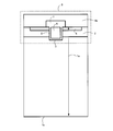
- FIG. 17 is an explanatory diagram showing a state in which cracks caused by polyimide occur during dicing.
- 17A is a plan view of the main part
- FIG. 17B is a cross-sectional view of the main part along the dicing line 73.
- an insulating film 57a is formed on the dicing line 73 on the front side of the wafer 51, and a collector electrode 62 which is a back electrode is formed on the back surface.
- the crack 83 extends to the portion A of the effective chip 71 and causes a deterioration in characteristics and a decrease in reliability of the effective chip 71.
- the present invention suppresses the occurrence of cracks due to polyimide when dicing a wafer along a dicing line with a blade, and prevents the occurrence of plating on the outer periphery of the wafer.
- An object of the present invention is to provide a semiconductor device manufacturing method capable of suppressing abnormal precipitation, extending the chemical life of the plating solution, and reducing the manufacturing cost.
- a method of manufacturing a semiconductor device includes a step of forming an invalid chip around the first main surface of a semiconductor wafer, Forming an effective chip in the region, forming a surface electrode on the effective chip and the ineffective chip, and disposing an insulating film on a dicing line that divides the effective chip and the ineffective chip, respectively.
- the semiconductor wafer is continuously covered from the outer peripheral edge of the semiconductor wafer to a portion away from the effective chip by a predetermined distance.
- the method for manufacturing a semiconductor device includes a step of forming an invalid chip around the first main surface of a semiconductor wafer, a step of forming an effective chip in a region surrounded by the invalid chip, and the effective Forming a surface electrode on the chip and the ineffective chip; disposing an insulating film on a dicing line that divides the effective chip and the ineffective chip; and a back surface on the second main surface of the semiconductor wafer
- a cutting direction in the first cutting direction, a direction intersecting with the dicing line, and a cutting end side in the first cutting direction are determined in advance, and the dicing line is sandwiched between invalid chips on the cutting end side of the dicing line in the cutting direction.
- the polyimide is continuously formed on the dicing line from the outer peripheral edge of the semiconductor wafer to a portion away from the effective chip by a predetermined distance, and the blade is cut along the dicing line in the first cutting direction.
- the semiconductor wafer is cut into semiconductor chips.
- the method for manufacturing a semiconductor device includes a step of forming an invalid chip around the first main surface of a semiconductor wafer, a step of forming an effective chip in a region surrounded by the invalid chip, and the effective A step of forming a surface electrode on the chip; a step of forming an insulating film on the ineffective chip; and a step of extending and disposing the insulating film on a dicing line that partitions the effective chip and the ineffective chip. And a step of forming a back electrode on the second main surface of the semiconductor wafer, and the semiconductor wafer so as to continuously cover from the outer peripheral edge of the semiconductor wafer to a portion away from the effective chip by a predetermined distance.
- the predetermined width of the polyimide covering the semiconductor wafer from the outer peripheral end is 2 mm or more and 10 mm or less.
- the predetermined width of the polyimide covering the semiconductor wafer from the outer peripheral end is 5 mm or more and 10 mm or less.
- the semiconductor device manufacturing method according to the present invention is characterized in that, in the above invention, a predetermined distance between the effective chip and the polyimide is 2 mm or more.
- the surface electrode is an aluminum electrode
- the insulating film is an oxide film
- the metal film is a nickel film laminated with a gold film.
- the plating is electroless plating
- the main electrode is a laminated film of an aluminum film, a nickel film and a gold film.
- FIG. 1 is an explanatory view (No. 1) showing a principal part manufacturing process of the semiconductor device according to the first embodiment of the present invention.
- FIG. 2 is an explanatory view (No. 2) showing a principal part manufacturing process of the semiconductor device according to the first embodiment of the present invention.
- FIG. 3 is an explanatory view (No. 3) showing a principal part manufacturing process of the semiconductor device according to the first embodiment of the present invention.
- FIG. 4 is an explanatory view (No. 4) showing the main part manufacturing process of the semiconductor device according to the first embodiment of the present invention.
- FIG. 5 is an explanatory view (No. 5) for explaining a principal part manufacturing process of the semiconductor device according to the first embodiment of the invention.
- FIG. 6 is an explanatory view (No.).
- FIG. 7 is an explanatory view (No. 7) showing the principal part manufacturing process of the semiconductor device according to the first embodiment of the invention.
- FIG. 8 is an explanatory diagram showing a cross section of the main part (cell) of the semiconductor device according to the first embodiment of the present invention.
- FIG. 9 is a diagram (part 1) illustrating a state of a crack generated on the back surface of the wafer.
- FIG. 10 is a diagram (part 2) illustrating a state of cracks generated on the back surface of the wafer.
- FIG. 11 is a main part manufacturing process diagram showing the second embodiment of the method for manufacturing a semiconductor device according to the present invention.
- FIG. 12 is a main part manufacturing process diagram showing the third embodiment of the method for manufacturing a semiconductor device according to the present invention.
- FIG. 13 is an explanatory diagram showing a cross-sectional structure of the main part of the FS-IGBT.
- FIG. 14 is an explanatory view showing a conventional wafer.
- FIG. 15 is an explanatory diagram showing a configuration of a wafer subjected to edge rinsing.
- FIG. 16 is an explanatory diagram showing a configuration of a wafer on which polyimide is not formed.
- FIG. 17 is an explanatory diagram showing a state in which cracks caused by polyimide occur during dicing.
- FIG. 2 FIG. 3, FIG. 4, FIG. 5, FIG. 6 and FIG. 7 are explanatory views showing the main steps of manufacturing the semiconductor device according to the first embodiment of the present invention.
- FIG. 8 is an explanatory diagram showing a cross section of the main part (cell) of the semiconductor device according to the first embodiment of the present invention.
- 1 to 7 show the main part of a semiconductor device manufactured according to the method of manufacturing a semiconductor device of the first embodiment according to the present invention in the order of steps.
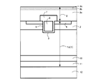
- FIG. 8 shows an FS-IGBT as an example of the semiconductor device according to the first embodiment of the present invention. Since the configuration of the FS-IGBT is the same as that of the FS-IGBT in FIG. 14, detailed description thereof is omitted.
- reference numeral 1a is an n silicon substrate (wafer 1)
- reference numeral 2 is a p-well layer
- reference numeral 3 is a trench
- reference numeral 4 is an n emitter layer
- reference numeral 5 is a gate oxide film
- reference numeral 6 is a gate electrode
- Reference numeral 7 denotes an interlayer insulating film
- reference numeral 8 denotes an emitter electrode
- reference numeral 8a denotes an aluminum electrode
- reference numeral 8b denotes a nickel film
- reference numeral 8c denotes a gold film
- reference numeral 10 denotes an n-FS layer
- reference numeral 11 denotes a p collector layer
- reference numeral 12 Indicates a collector electrode.
- the gate pad is not shown.
- the emitter electrode 8 includes an aluminum electrode 8a and a nickel film 8b and a gold film 8c that cover the aluminum electrode 8a.
- n silicon substrate 1a wafer 1
- a p well layer 2 a p well layer 2
- an n emitter layer 4 a gate electrode 6 and an aluminum electrode 8a (surface electrode, emitter)
- a surface structure portion 9 such as a part of the electrode 8 is formed.
- An interlayer insulating film 7 is formed between the gate electrode 6 and the aluminum electrode 8a.
- the aluminum electrode 8a can be formed of an aluminum / silicon (Al—Si) film or an aluminum / silicon / copper (Al—Si—Cu) film in addition to the aluminum (Al) film.
- the protective tape 9a is peeled off. Further, this ground surface is wet etched. By this wet etching, the thick wafer (n silicon substrate) 1a is made into a thin wafer 1 having a thickness of about 150 ⁇ m, for example. This thickness differs depending on the breakdown voltage of the FS-IGBT.
- phosphorus and boron are ion-implanted into the back surface 1b and annealed to form the n-FS layer 10 and the p collector layer 11.
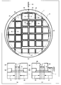
- FIG. 4 shows the wafer of this example, and shows the structure of the wafer formed up to polyimide.
- (a) is a plan view of the main part
- (b) is a cross-sectional view of the main part of (a) cut by X1-X1
- (c) is a cross-sectional view of the main part of (a) cut by X2-X2. Is shown.
- polyimide 25 on the outer periphery and 26 on the inner polyimide
- the insulating film 7a is an insulating film or a field oxide film formed simultaneously with the interlayer insulating film 7.
- FIG. 4B shows a case where the breakdown voltage structure 20 (for example, RESURF structure) of the effective chip 21 is covered with the insulating film 7 a and the insulating film 7 a is further covered with the polyimide 26.
- the breakdown voltage structure 20 is entirely covered with the insulating film 7a as shown in FIG. 4, only the emitter electrode 8a of the ineffective chip 22 is covered, The insulating film 7a may be exposed.
- a metal electrode such as a guard ring is exposed as the pressure-resistant structure portion 20
- deposition of a plating film on the metal electrode of the pressure-resistant structure portion 20 is prevented in a later process to protect the pressure-resistant structure.
- the pressure-resistant structure 20 is also covered with the polyimide 26.
- the effective chip 21 is a chip that is arranged at the center of the wafer 1 and becomes effective when the chip is formed. More specifically, it is a chip in which the distance L from the end portion 25a of the polyimide 25 on the outer peripheral portion is 2 mm or more.
- the invalid chip 22 is a chip which is disposed on the outer periphery of the wafer 1 and has no corners or a necessary process such as film formation is incomplete, which is not useful as an element.
- the part where the polyimide 26 on the dicing line 23 is removed extends to the dicing line 23 sandwiched between the ineffective chips 22 (the part where the reference numeral 28 extends).
- the insulating film 7a is exposed from the removed portion.
- the insulating film 7a is, for example, a BPSG (boron phosphorus glass) film.
- the width W from the wafer end 1c is set to 2 mm or more. If the width W is less than 2 mm, as described in the prior art, silicon or polysilicon is exposed by edge rinse, and abnormal deposition of the plating film may occur there. Further, it is preferable to set the width W to 5 mm or more because the polysilicon and silicon exposed by the edge rinse are more reliably covered. However, if the width W is excessively widened, the number of effective chips 21 that can be taken decreases.
- this crack (see reference numeral 33 in FIG. 9) generated at the time of dicing may spread on the back surface of the effective chip 21 and may have an adverse effect. Therefore, the minimum distance W between the effective chip 21 and the outer peripheral polyimide 25 is set to 2 mm or more. If it is less than 2 mm, the crack 33 generated in the dicing line 23 may reach the effective chip 21 in some cases.
- the width of the dicing line 23 is about 80 ⁇ m, for example.
- the crack generated on the back surface of the effective chip 21 will be described later (see FIG. 9).
- reference numeral 24 denotes a center line of the dicing line 23
- reference numeral 27 denotes an orientation flat (OF).
- a back electrode (collector electrode 12) is formed on the back surface 1b of the wafer 1 by sputtering.
- the collector electrode 12 is formed of a laminated film of an aluminum film 12a (or aluminum / silicon film) / titanium film 12b / nickel film 12c / gold film 12d from the surface of the wafer 1.
- the collector electrode 12 on the back surface 1b of the wafer 1 is attached to a glass plate 29, and the whole is placed in an electroless plating layer, and a nickel film 8b, gold on the aluminum electrode 8a on the wafer surface.
- the emitter electrode 8 is formed by sequentially electrolessly plating the film 8c.
- the reason why the surface of the aluminum electrode 8a is made of the nickel film 8b and the gold film 8c is that it is necessary for soldering with an external lead-out conductor (external lead wiring).
- the process (4) may be performed before the process (2). In that case, the order of steps (1), (4), (2), (3), (5) and (6) is applied. Further, the step (1) of forming the aluminum electrode 8a may be performed after the step (3).
- the chip is diced (cut) along the center line 24 of the dicing line 23 of the wafer 1 with a blade 32 (diamond cutter) having a diameter of about 50 mm.
- the cutting width (dicing width) when the dicing line 23 is diced with the blade of the blade 32 is, for example, about 40 ⁇ m.
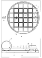
- FIG. 7 shows how the wafer 1 is diced in the direction indicated by the arrow from the upper side to the lower OF 27 in FIG. 7 denotes a dicing tape to which the wafer 1 is attached.
- the aluminum electrode 8a of the invalid chip 22 since the polyimide is coated on the aluminum electrode 8a of the invalid chip 22, the aluminum electrode 8a is not plated. Therefore, the area to be plated (plating deposition area) is narrowed, and the chemical life of the electroless plating solution can be extended. As a result, the manufacturing cost can be reduced.
- FIG. 9 is a diagram (No. 1) for explaining the state of the crack 33 generated on the back surface of the wafer 1.
- the dicing line 23 is first diced.
- FIG. 9A shows a state where the blade 32 is inserted from the wafer end 1c. The case (start of cutting) is shown, and (b) shows the case where the blade 32 is separated from the wafer end 1c (end of cutting).
- the dicing line 23 sandwiched between the invalid chips 22 is covered with polyimides 25 and 26.
- the width W of the polyimide 25 at the outer peripheral portion is 2 mm.
- An emitter electrode 8 and a collector electrode 12 are formed on the wafer 1, but are omitted for the sake of simplicity.
- the crack 33 is introduced from the wafer end 1c, and the crack 33 is finished in the polyimide 26a. Further, as shown in FIG. 9B, the crack 33 is introduced from the front (polyimide end portion 26b) immediately below the polyimide 26a, and the crack 33 ends in the polyimide 26a.
- the distance T in front is less than 2 mm, and most is about 1 mm.
- the crack 33 since the crack 33 has occurred in the polyimide 26a, the crack 33 does not extend to the effective chip 21.
- the crack 32 is started before the polyimide 26a immediately below the polyimide 26a.
- the crack is formed on the back surface of the effective chip 21. 33 may be stretched.
- FIG. 10 is a diagram (No. 2) for explaining the state of the crack 33 generated on the back surface of the wafer 1.
- either the vertical or horizontal dicing line 23 is cut (diced) by the blade 32, and then cut along the uncut dicing line 23 orthogonal to the cut dicing line 23 a
- the state of the crack 33 generated on the back surface of the wafer 1 by this cutting when the dicing is performed (after being cut becomes the cut dicing line 23a)
- (a) shows the blade 32 inserted from the wafer end 1c.
- B shows a case where the blade 32 is separated from the wafer end 1c (end of cutting).
- the crack 33 is introduced from the wafer end 1c, and the crack 33 is finished in the polyimide 26a. Further, as shown in FIG. 10B, a crack 33 is introduced from directly under the polyimide 26a, and the crack 33 ends within the polyimide 26a. In any of the cases of FIG. 10, the crack 33 is generated in the polyimide 26 a in any case, and the crack 33 does not reach the effective chip 21, so that the effective chip 21 is not adversely affected.
- the location where the crack 33 is generated away from the inside of the polyimide 26a is the location where the blade 32 is separated from the wafer 1 in the dicing line 23 where the blade 32 is first inserted. Based on this, an example in which the generation of cracks 33 is suppressed will be described in the second embodiment.
- FIG. 11 is a main part manufacturing process diagram showing the second embodiment of the method for manufacturing a semiconductor device according to the present invention. 11, (a) is a plan view of the main part, (b) is a cross-sectional view of the main part of (a) cut by X1-X1, and (c) is a cross-sectional view of the main part of (a) cut by X2-X2. Is shown.
- the polyimide 26 on the dicing line 23 sandwiched between the invalid chips 22 near the end point of the dicing line 23 in which the blade 32 is inserted first is removed.
- the difference from Embodiment 1 is that the polyimide on the dicing line 23 adjacent to the invalid chip 22 is left.
- the numbers (1) to (13) in parentheses indicate the dicing order, and the arrows indicate the dicing direction.
- the dicing lines 1 to 7 ((1) to (7)) of the vertical dicing line 23 are diced. This direction is the direction to cut first. Thereafter, dicing is performed on the horizontal dicing line 23 from No. 8 to No. 13 (from (8) to (13)).
- the upper end of the wafer 1 is the insertion point of the blade 32 in the first to seventh dicing lines 23 in the vertical direction, and the OF 27 at the lower end of the wafer 1 is the end point of the blade 32.
- the inner polyimide 26 is removed leaving the outer peripheral polyimide 25 on the end point dicing line 23 (region B in FIG. 11).
- the crack 33 is formed on the outer peripheral portion of the dicing line 23 sandwiched between the invalid chips 22. It occurs when the distance T is about 1 mm (at most, less than 2 mm) from the polyimide directly under 26a and the polyimide end 25a.
- the effective chip 21 is 2 mm or more away from the polyimide end portion 25a (distance L shown in FIG. 4), the crack 33 generated at the outer peripheral portion 1 immediately below the polyimide does not reach the effective chip 21. Therefore, the effective chip 21 is not adversely affected.
- the vertical dicing line Nos. 1 to 7 are cut, so that the effective chip 21 and the ineffective chip 22 are partitioned.
- the vertical dicing line 23a has been cut. For this reason, even if the crack 33 is generated in the polyimide 26a due to the 8th to 13th cuts in the lateral direction, the crack does not reach the effective chip 21 beyond the cut dicing line. Therefore, the effective chip 21 is not adversely affected.
- the position where the blade 32 is introduced when the wafer 1 is cut and which of the vertical and horizontal dicing lines 23 (23a) is cut first is determined. This is an effective method.
- the longitudinal direction (the direction toward the orientation flat 27) is the first cutting direction, but the cutting direction is not limited to this.
- the longitudinal direction opposite to the cutting direction shown in FIG. 11 may be used, or the horizontal direction (direction parallel to the orientation flat 27) may be set as the initial cutting direction.
- tip is inclined and arrange
- the effective chip from the outer peripheral edge of the semiconductor wafer is placed on the dicing line sandwiched between the ineffective chips on the side where the cutting is completed for the dicing line in the first cutting direction. Is continuously covered up to a predetermined distance. In other words, on the dicing line sandwiched between the ineffective chips on the cutting end side, polyimide is not formed in a portion at a predetermined distance from the effective chip. If the order of cutting directions is not determined in advance, the method of the first embodiment may be applied.
- FIG. 12 is a main part manufacturing process diagram showing the third embodiment of the method for manufacturing a semiconductor device according to the present invention. 12, (a) is a plan view of the main part, (b) is a cross-sectional view of the main part of (a) cut along X1-X1, and (c) is a cross-sectional view of the main part of (a) cut along X2-X2. Is shown.
- the insulating film 7a on the dicing line 23 is extended and covered without forming the aluminum electrode 8a on the surface of the ineffective chip 22. Different from 1.
- the polyimide 25 is coated only on the outer peripheral portion of the wafer 1 in the step (4) described above. For this reason, the crack 33 is generated just under the polyimide 26a, or reaches only a portion about 1 mm inside from the polyimide end 25a even when entering from the polyimide end 25a. Since the effective chip 21 is separated from the polyimide end portion 25 a by 2 mm or more, the crack 33 does not reach the effective chip 21 and does not adversely affect the effective chip 21.
- the aluminum electrode 8a is not formed on the ineffective chip 22 and the insulating film 7a is covered, it is not plated. Therefore, the chemical life of the electroless plating solution can be extended, and the manufacturing cost can be reduced. Further, since the outer peripheral portion of the wafer 1 is coated with the polyimide 25, abnormal precipitation due to electroless plating does not occur.
- the manufacturing method of the apparatus is not limited to the manufacturing of the FS-IGBT.
- the method for manufacturing a semiconductor device according to the present invention can also be applied to the manufacture of IGBTs, MOSFETs, diodes, etc. other than FS-IGBTs.
- the outer periphery of the wafer and the invalid chip are each coated with polyimide, and the polyimide on the dicing line sandwiched between the invalid chips is removed, so that the effective chip can be obtained by dicing with the blade.
- produces in the back surface of can be suppressed.
- the present invention by covering the location of the ineffective chip with polyimide, it is possible to prevent the location from being plated, the chemical solution life of the plating solution can be extended, and the manufacturing cost can be reduced. .
- the outer peripheral portion of the wafer is coated with polyimide, and the upper surface of the ineffective chip is covered with an oxide film to suppress cracks generated on the back surface of the effective chip by dicing with the blade, Abnormal deposition due to electroless plating generated on the outer peripheral side wall of the wafer can be suppressed, and further, the chemical life of the plating solution can be extended, and the manufacturing cost can be reduced.
- the present invention relates to a semiconductor device manufacturing method, and is particularly suitable for a semiconductor device manufacturing method for manufacturing a semiconductor wafer (hereinafter simply referred to as a wafer) by dicing with a blade.
- a semiconductor wafer hereinafter simply referred to as a wafer
Landscapes
- Internal Circuitry In Semiconductor Integrated Circuit Devices (AREA)
- Dicing (AREA)
- Formation Of Insulating Films (AREA)
Abstract
Description
まず、この発明にかかる半導体装置の製造方法の実施の形態1について説明する。図1、図2、図3、図4、図5、図6および図7は、この発明にかかる実施の形態1の半導体装置の要部製造工程を示す説明図である。図8は、この発明にかかる実施の形態1の半導体装置の要部(セル)断面を示す説明図である。図1~図7においては、この発明にかかる実施の形態1の半導体装置の製造方法にしたがって製造した半導体装置の要部を、工程順に示している。図8においては、この発明にかかる実施の形態1の半導体装置の一例としてFS-IGBTを示している。FS-IGBTの構成は、図14のFS-IGBTと同じであるため、その詳細な説明は省略する。
つぎに、この発明にかかる半導体装置の製造方法の実施の形態2について説明する。図11は、この発明にかかる半導体装置の製造方法の実施の形態2を示す要部製造工程図である。図11において、(a)は要部平面図、(b)は(a)をX1-X1で切断した要部断面図、(c)は(a)をX2-X2で切断した要部断面図を示している。
つぎに、この発明にかかる半導体装置の製造方法の実施の形態3について説明する。図12は、この発明にかかる半導体装置の製造方法の実施の形態3を示す要部製造工程図である。図12において、(a)は要部平面図、(b)は(a)をX1-X1で切断した要部断面図、(c)は(a)をX2-X2で切断した要部断面図を示している。実施の形態3は、上述した(4)の工程において、無効チップ22の表面にアルミ電極8aを形成せずにダイシングライン23上の絶縁膜7aを延在させて被覆した点が、実施の形態1と異なる。
1a ウェハ(厚い)
1b ウェハの裏面
1c ウェハの端部
2 pウェル層
3 トレンチ
4 nエミッタ層
5 ゲート酸化膜
6 ゲート電極
7 層間絶縁膜
7a 絶縁膜
8 エミッタ電極
8a アルミ電極
8b ニッケル膜
8c 金膜
9 表面構造部
10 n-FS層
11 pコレクタ層
12 コレクタ電極
12a アルミ膜
12b チタン膜
12c ニッケル膜
12d 金膜
20 耐圧構造部
21 有効チップ
22 無効チップ
23 ダイシングライン
24 中心線
25 ポリイミド(外周部)
25a ポリイミド25の端部
26 ポリイミド(内側)
26a ポリイミド直下
26b ポリイミド26の端部
27 オリエンテーションフラット(OF)
28 伸びている箇所
29 ガラス板
31 ダイシングテープ
32 ブレード
33 クラック
Claims (7)
- 半導体ウェハの第1主面の周囲に無効チップを形成する工程と、
前記無効チップで囲まれた領域に有効チップを形成する工程と、
前記有効チップ上と前記無効チップ上とに表面電極を形成する工程と、
前記有効チップおよび前記無効チップをそれぞれ区画するダイシングライン上に絶縁膜を配置する工程と、
前記半導体ウェハの第2主面に裏面電極を形成する工程と、
前記半導体ウェハの外周端から内側へ向かって連続して前記無効チップを覆うとともに、前記無効チップに挟まれたダイシングライン上であって前記半導体ウェハの外周端から前記有効チップに対して所定の距離離れた部分までを連続して覆うように、前記半導体ウェハの前記第1主面の外周部を前記半導体ウェハの外周端から所定の幅で覆うポリイミドを形成する工程と、
前記有効チップ上に形成された前記表面電極上にメッキで金属膜を被覆する工程と、
前記ダイシングラインに沿ってブレードで前記半導体ウェハを切断し半導体チップにする工程と、
を含んだことを特徴とする半導体装置の製造方法。 - 半導体ウェハの第1主面の周囲に無効チップを形成する工程と、
前記無効チップで囲まれた領域に有効チップを形成する工程と、
前記有効チップ上と前記無効チップ上とに表面電極を形成する工程と、
前記有効チップおよび前記無効チップをそれぞれ区画するダイシングライン上に絶縁膜を配置する工程と、
前記半導体ウェハの第2主面に裏面電極を形成する工程と、
前記半導体ウェハの第1主面の外周部を前記半導体ウェハの外周端から所定の幅で覆うポリイミドを形成する工程と、
前記有効チップ上に配置される前記表面電極上にメッキで金属膜を被覆する工程と、
を含み、
前記ポリイミドを形成する工程は、前記半導体ウェハの外周端から内側へ向かって連続して前記無効チップを覆うとともに、
前記ダイシングラインについて、最初に切断する方向とこれに交差する方向および最初に切断する方向の切り終える側を予め定め、最初に切断する方向のダイシングラインの切り終える側の無効チップに挟まれたダイシングライン上を、半導体ウェハの外周端から有効チップに対して所定の距離離れた部分までを連続して覆うポリイミドを形成し、
前記最初に切断する方向のダイシングラインに沿って前記ブレードで前記半導体ウェハを切断し半導体チップにすることを特徴とする半導体装置の製造方法。 - 半導体ウェハの第1主面の周囲に無効チップを形成する工程と、
前記無効チップで囲まれた領域に有効チップを形成する工程と、
前記有効チップ上に表面電極を形成する工程と、
前記無効チップ上に絶縁膜を形成する工程と、
前記有効チップおよび前記無効チップをそれぞれ区画するダイシングライン上に前記絶縁膜を延在して配置する工程と、
前記半導体ウェハの第2主面に裏面電極を形成する工程と、
前記半導体ウェハの外周端から前記有効チップに対して所定の距離離れた部分までを連続して覆うように、前記半導体ウェハの第1主面の外周部を前記半導体ウェハの外周端から所定の幅で覆うポリイミドを形成する工程と、
前記有効チップ上に配置される前記表面電極上にメッキで金属膜を被覆する工程と、
前記ダイシングラインに沿ってブレードで前記半導体ウェハを切断し半導体チップにする工程と、
を含んだことを特徴とする半導体装置の製造方法。 - 前記半導体ウェハを外周端から覆うポリイミドの前記所定の幅は、2mm以上10mm以下であることを特徴とする請求項1~3のいずれか一項に記載の半導体装置の製造方法。
- 前記半導体ウェハを外周端から覆うポリイミドの前記所定の幅は、5mm以上10mm以下であることを特徴とする請求項1~3のいずれか一項に記載の半導体装置の製造方法。
- 前記有効チップと前記ポリイミドとの所定の距離は、2mm以上であることを特徴とする請求項1~3のいずれか一項に記載の半導体装置の製造方法。
- 前記表面電極がアルミ電極であり、
前記絶縁膜が酸化膜であり、
前記金属膜がニッケル膜に金膜を積層したメッキ膜であり、
前記メッキが無電解メッキであり、
前記主電極がアルミニウム膜、ニッケル膜および金膜の積層膜であることを特徴とする請求項1~3のいずれか一項に記載の半導体装置の製造方法。
Priority Applications (4)
| Application Number | Priority Date | Filing Date | Title |
|---|---|---|---|
| JP2012535042A JP5609981B2 (ja) | 2010-09-22 | 2011-09-20 | 半導体装置の製造方法 |
| US13/817,112 US8865567B2 (en) | 2010-09-22 | 2011-09-20 | Method of manufacturing semiconductor device |
| CN201180039092.9A CN103069546B (zh) | 2010-09-22 | 2011-09-20 | 半导体器件的制造方法 |
| EP11826848.1A EP2587525B1 (en) | 2010-09-22 | 2011-09-20 | Method of manufacturing semiconductor device |
Applications Claiming Priority (2)
| Application Number | Priority Date | Filing Date | Title |
|---|---|---|---|
| JP2010-211487 | 2010-09-22 | ||
| JP2010211487 | 2010-09-22 |
Publications (1)
| Publication Number | Publication Date |
|---|---|
| WO2012039403A1 true WO2012039403A1 (ja) | 2012-03-29 |
Family
ID=45873887
Family Applications (1)
| Application Number | Title | Priority Date | Filing Date |
|---|---|---|---|
| PCT/JP2011/071408 Ceased WO2012039403A1 (ja) | 2010-09-22 | 2011-09-20 | 半導体装置の製造方法 |
Country Status (5)
| Country | Link |
|---|---|
| US (1) | US8865567B2 (ja) |
| EP (1) | EP2587525B1 (ja) |
| JP (1) | JP5609981B2 (ja) |
| CN (1) | CN103069546B (ja) |
| WO (1) | WO2012039403A1 (ja) |
Cited By (2)
| Publication number | Priority date | Publication date | Assignee | Title |
|---|---|---|---|---|
| KR20180082334A (ko) * | 2017-01-10 | 2018-07-18 | 르네사스 일렉트로닉스 가부시키가이샤 | 반도체 장치의 제조 방법 및 반도체 웨이퍼 |
| US12575372B2 (en) | 2021-11-19 | 2026-03-10 | Mitsubishi Electric Corporation | Semiconductor wafer and method for manufacturing semiconductor wafer |
Families Citing this family (6)
| Publication number | Priority date | Publication date | Assignee | Title |
|---|---|---|---|---|
| JP6265594B2 (ja) | 2012-12-21 | 2018-01-24 | ラピスセミコンダクタ株式会社 | 半導体装置の製造方法、及び半導体装置 |
| USD720313S1 (en) * | 2014-06-16 | 2014-12-30 | Emcore Solar Power, Inc. | Semiconductor wafer with dicing positions for solar cell fabrication |
| TWD174921S (zh) * | 2014-12-17 | 2016-04-11 | 日本碍子股份有限公司 | 複合基板之部分 |
| CN109616414A (zh) * | 2018-11-06 | 2019-04-12 | 深圳方正微电子有限公司 | 晶圆加工方法和半导体器件的制备方法 |
| KR102935507B1 (ko) | 2020-08-20 | 2026-03-06 | 삼성전자주식회사 | 반도체 기판 및 반도체 기판의 소잉 방법 |
| USD1118897S1 (en) | 2021-09-08 | 2026-03-17 | Lam Research Corporation | Debubbler component |
Citations (5)
| Publication number | Priority date | Publication date | Assignee | Title |
|---|---|---|---|---|
| JPH05315304A (ja) * | 1992-05-12 | 1993-11-26 | Sony Corp | ウエハの裏面研削方法 |
| JP2005244165A (ja) * | 2004-01-30 | 2005-09-08 | Denso Corp | 半導体チップの製造方法 |
| JP2006032390A (ja) * | 2004-07-12 | 2006-02-02 | Seiko Epson Corp | ダイシングシートおよびその製造方法、半導体装置の製造方法 |
| JP2007036129A (ja) * | 2005-07-29 | 2007-02-08 | Renesas Technology Corp | 半導体装置の製造方法 |
| JP2007287780A (ja) * | 2006-04-13 | 2007-11-01 | Toshiba Corp | 半導体装置の製造方法及び半導体装置 |
Family Cites Families (2)
| Publication number | Priority date | Publication date | Assignee | Title |
|---|---|---|---|---|
| JP3094939B2 (ja) * | 1997-03-19 | 2000-10-03 | 株式会社村田製作所 | 電子部品の製造方法 |
| JP2007214268A (ja) * | 2006-02-08 | 2007-08-23 | Seiko Instruments Inc | 半導体装置の製造方法 |
-
2011
- 2011-09-20 WO PCT/JP2011/071408 patent/WO2012039403A1/ja not_active Ceased
- 2011-09-20 JP JP2012535042A patent/JP5609981B2/ja active Active
- 2011-09-20 CN CN201180039092.9A patent/CN103069546B/zh active Active
- 2011-09-20 EP EP11826848.1A patent/EP2587525B1/en active Active
- 2011-09-20 US US13/817,112 patent/US8865567B2/en active Active
Patent Citations (5)
| Publication number | Priority date | Publication date | Assignee | Title |
|---|---|---|---|---|
| JPH05315304A (ja) * | 1992-05-12 | 1993-11-26 | Sony Corp | ウエハの裏面研削方法 |
| JP2005244165A (ja) * | 2004-01-30 | 2005-09-08 | Denso Corp | 半導体チップの製造方法 |
| JP2006032390A (ja) * | 2004-07-12 | 2006-02-02 | Seiko Epson Corp | ダイシングシートおよびその製造方法、半導体装置の製造方法 |
| JP2007036129A (ja) * | 2005-07-29 | 2007-02-08 | Renesas Technology Corp | 半導体装置の製造方法 |
| JP2007287780A (ja) * | 2006-04-13 | 2007-11-01 | Toshiba Corp | 半導体装置の製造方法及び半導体装置 |
Non-Patent Citations (1)
| Title |
|---|
| See also references of EP2587525A4 * |
Cited By (3)
| Publication number | Priority date | Publication date | Assignee | Title |
|---|---|---|---|---|
| KR20180082334A (ko) * | 2017-01-10 | 2018-07-18 | 르네사스 일렉트로닉스 가부시키가이샤 | 반도체 장치의 제조 방법 및 반도체 웨이퍼 |
| KR102481682B1 (ko) | 2017-01-10 | 2022-12-28 | 르네사스 일렉트로닉스 가부시키가이샤 | 반도체 장치의 제조 방법 및 반도체 웨이퍼 |
| US12575372B2 (en) | 2021-11-19 | 2026-03-10 | Mitsubishi Electric Corporation | Semiconductor wafer and method for manufacturing semiconductor wafer |
Also Published As
| Publication number | Publication date |
|---|---|
| US8865567B2 (en) | 2014-10-21 |
| CN103069546B (zh) | 2016-05-04 |
| EP2587525B1 (en) | 2020-03-25 |
| EP2587525A4 (en) | 2017-07-26 |
| JP5609981B2 (ja) | 2014-10-22 |
| US20130203238A1 (en) | 2013-08-08 |
| EP2587525A1 (en) | 2013-05-01 |
| CN103069546A (zh) | 2013-04-24 |
| JPWO2012039403A1 (ja) | 2014-02-03 |
Similar Documents
| Publication | Publication Date | Title |
|---|---|---|
| JP5609981B2 (ja) | 半導体装置の製造方法 | |
| JP6061726B2 (ja) | 半導体装置および半導体ウェハ | |
| TWI262537B (en) | Semiconductor device with crack prevention ring and method of manufacture thereof | |
| JP4349278B2 (ja) | 半導体装置の製造方法 | |
| US7994614B2 (en) | Semiconductor wafer, semiconductor device, and method of manufacturing semiconductor device | |
| US9831193B1 (en) | Methods and apparatus for scribe street probe pads with reduced die chipping during wafer dicing | |
| US10157861B2 (en) | Crack propagation prevention and enhanced particle removal in scribe line seals of semiconductor devices | |
| US10403554B2 (en) | Method for manufacturing semiconductor device | |
| JP4815905B2 (ja) | 半導体装置およびその製造方法 | |
| TW200416854A (en) | Semiconductor device and fabrication method thereof | |
| CN108364865A (zh) | 半导体器件制造方法和半导体晶片 | |
| US8987923B2 (en) | Semiconductor seal ring | |
| US8067819B2 (en) | Semiconductor wafer including semiconductor chips divided by scribe line and process-monitor electrode pads formed on scribe line | |
| CN115152034A (zh) | 半导体装置 | |
| CN108511415B (zh) | 电子组件制造方法 | |
| CN1417867A (zh) | 集成型肖特基势垒二极管及其制造方法 | |
| JPS62112348A (ja) | 半導体装置の製造方法 | |
| JP2013134998A (ja) | 半導体装置およびその製造方法 | |
| JP7131155B2 (ja) | 半導体装置 | |
| JP7559954B2 (ja) | 半導体ウェハ | |
| TW201105193A (en) | Cutting process of circuit board | |
| JP2015103705A (ja) | 半導体装置の製造方法および半導体装置ならびに半導体製造装置 | |
| JP2026001384A (ja) | 半導体装置および半導体装置の製造方法 | |
| CN113410214A (zh) | 一种半导体器件结构及其制造方法 | |
| KR20240138768A (ko) | 기계적 절삭을 이용한 반도체 칩 분할 방법 및 이를 통해 분할된 반도체 칩 |
Legal Events
| Date | Code | Title | Description |
|---|---|---|---|
| WWE | Wipo information: entry into national phase |
Ref document number: 201180039092.9 Country of ref document: CN |
|
| 121 | Ep: the epo has been informed by wipo that ep was designated in this application |
Ref document number: 11826848 Country of ref document: EP Kind code of ref document: A1 |
|
| WWE | Wipo information: entry into national phase |
Ref document number: 2012535042 Country of ref document: JP |
|
| WWE | Wipo information: entry into national phase |
Ref document number: 2011826848 Country of ref document: EP |
|
| NENP | Non-entry into the national phase |
Ref country code: DE |
|
| WWE | Wipo information: entry into national phase |
Ref document number: 13817112 Country of ref document: US |