WO2012043542A1 - コネクタ及び電子機器 - Google Patents
コネクタ及び電子機器 Download PDFInfo
- Publication number
- WO2012043542A1 WO2012043542A1 PCT/JP2011/072038 JP2011072038W WO2012043542A1 WO 2012043542 A1 WO2012043542 A1 WO 2012043542A1 JP 2011072038 W JP2011072038 W JP 2011072038W WO 2012043542 A1 WO2012043542 A1 WO 2012043542A1
- Authority
- WO
- WIPO (PCT)
- Prior art keywords
- connector
- case
- connector member
- contact
- inner shield
- Prior art date
- Legal status (The legal status is an assumption and is not a legal conclusion. Google has not performed a legal analysis and makes no representation as to the accuracy of the status listed.)
- Ceased
Links
Images






Classifications
-
- H—ELECTRICITY
- H01—ELECTRIC ELEMENTS
- H01R—ELECTRICALLY-CONDUCTIVE CONNECTIONS; STRUCTURAL ASSOCIATIONS OF A PLURALITY OF MUTUALLY-INSULATED ELECTRICAL CONNECTING ELEMENTS; COUPLING DEVICES; CURRENT COLLECTORS
- H01R13/00—Details of coupling devices of the kinds covered by groups H01R12/70 or H01R24/00 - H01R33/00
- H01R13/648—Protective earth or shield arrangements on coupling devices, e.g. anti-static shielding
-
- H—ELECTRICITY
- H01—ELECTRIC ELEMENTS
- H01R—ELECTRICALLY-CONDUCTIVE CONNECTIONS; STRUCTURAL ASSOCIATIONS OF A PLURALITY OF MUTUALLY-INSULATED ELECTRICAL CONNECTING ELEMENTS; COUPLING DEVICES; CURRENT COLLECTORS
- H01R13/00—Details of coupling devices of the kinds covered by groups H01R12/70 or H01R24/00 - H01R33/00
- H01R13/648—Protective earth or shield arrangements on coupling devices, e.g. anti-static shielding
- H01R13/658—High frequency shielding arrangements, e.g. against EMI [Electro-Magnetic Interference] or EMP [Electro-Magnetic Pulse]
- H01R13/6591—Specific features or arrangements of connection of shield to conductive members
- H01R13/6594—Specific features or arrangements of connection of shield to conductive members the shield being mounted on a PCB and connected to conductive members
-
- H—ELECTRICITY
- H01—ELECTRIC ELEMENTS
- H01R—ELECTRICALLY-CONDUCTIVE CONNECTIONS; STRUCTURAL ASSOCIATIONS OF A PLURALITY OF MUTUALLY-INSULATED ELECTRICAL CONNECTING ELEMENTS; COUPLING DEVICES; CURRENT COLLECTORS
- H01R13/00—Details of coupling devices of the kinds covered by groups H01R12/70 or H01R24/00 - H01R33/00
- H01R13/46—Bases; Cases
- H01R13/516—Means for holding or embracing insulating body, e.g. casing, hoods
-
- H—ELECTRICITY
- H01—ELECTRIC ELEMENTS
- H01R—ELECTRICALLY-CONDUCTIVE CONNECTIONS; STRUCTURAL ASSOCIATIONS OF A PLURALITY OF MUTUALLY-INSULATED ELECTRICAL CONNECTING ELEMENTS; COUPLING DEVICES; CURRENT COLLECTORS
- H01R13/00—Details of coupling devices of the kinds covered by groups H01R12/70 or H01R24/00 - H01R33/00
- H01R13/62—Means for facilitating engagement or disengagement of coupling parts or for holding them in engagement
- H01R13/627—Snap or like fastening
- H01R13/6271—Latching means integral with the housing
-
- H—ELECTRICITY
- H01—ELECTRIC ELEMENTS
- H01R—ELECTRICALLY-CONDUCTIVE CONNECTIONS; STRUCTURAL ASSOCIATIONS OF A PLURALITY OF MUTUALLY-INSULATED ELECTRICAL CONNECTING ELEMENTS; COUPLING DEVICES; CURRENT COLLECTORS
- H01R12/00—Structural associations of a plurality of mutually-insulated electrical connecting elements, specially adapted for printed circuits, e.g. printed circuit boards [PCB], flat or ribbon cables, or like generally planar structures, e.g. terminal strips, terminal blocks; Coupling devices specially adapted for printed circuits, flat or ribbon cables, or like generally planar structures; Terminals specially adapted for contact with, or insertion into, printed circuits, flat or ribbon cables, or like generally planar structures
- H01R12/70—Coupling devices
- H01R12/71—Coupling devices for rigid printing circuits or like structures
- H01R12/72—Coupling devices for rigid printing circuits or like structures coupling with the edge of the rigid printed circuits or like structures
- H01R12/722—Coupling devices for rigid printing circuits or like structures coupling with the edge of the rigid printed circuits or like structures coupling devices mounted on the edge of the printed circuits
- H01R12/724—Coupling devices for rigid printing circuits or like structures coupling with the edge of the rigid printed circuits or like structures coupling devices mounted on the edge of the printed circuits containing contact members forming a right angle
-
- H—ELECTRICITY
- H01—ELECTRIC ELEMENTS
- H01R—ELECTRICALLY-CONDUCTIVE CONNECTIONS; STRUCTURAL ASSOCIATIONS OF A PLURALITY OF MUTUALLY-INSULATED ELECTRICAL CONNECTING ELEMENTS; COUPLING DEVICES; CURRENT COLLECTORS
- H01R13/00—Details of coupling devices of the kinds covered by groups H01R12/70 or H01R24/00 - H01R33/00
- H01R13/46—Bases; Cases
- H01R13/502—Bases; Cases composed of different pieces
- H01R13/506—Bases; Cases composed of different pieces assembled by snap action of the parts
-
- H—ELECTRICITY
- H01—ELECTRIC ELEMENTS
- H01R—ELECTRICALLY-CONDUCTIVE CONNECTIONS; STRUCTURAL ASSOCIATIONS OF A PLURALITY OF MUTUALLY-INSULATED ELECTRICAL CONNECTING ELEMENTS; COUPLING DEVICES; CURRENT COLLECTORS
- H01R13/00—Details of coupling devices of the kinds covered by groups H01R12/70 or H01R24/00 - H01R33/00
- H01R13/648—Protective earth or shield arrangements on coupling devices, e.g. anti-static shielding
- H01R13/658—High frequency shielding arrangements, e.g. against EMI [Electro-Magnetic Interference] or EMP [Electro-Magnetic Pulse]
- H01R13/6591—Specific features or arrangements of connection of shield to conductive members
- H01R13/6596—Specific features or arrangements of connection of shield to conductive members the conductive member being a metal grounding panel
Definitions
- the present invention relates to a connector for electrical connection and an electronic device including the connector.
- FIG. 1 is an exploded perspective view of a connector described in Patent Document 1.
- the connector 40 includes a main housing 1, a connector housing 2, an inner shield case 3, and an outer shield case 5.
- the inner shield case 3 is inserted into a connector housing 2 made of an insulator.
- a connector housing 2 is inserted into the main housing 1.
- the protrusions 19 a and 19 b formed on the connector housing 2 are fitted in the grooves 10 a and 10 b of the main housing 1, respectively, so that the connector housing 2 is fixed to the main housing 1.
- An outer shield case 5 is attached so as to cover the main housing 1. With such a structure, the connector 40 achieves a double shield structure.
- a flat plate-shaped plug contact portion 4 is formed inside the connector housing 2.
- Connection portions 4 a are formed on both plate surfaces of the plug contact portion 4.
- a plurality of upper terminals 12 and lower terminals 13, which are elongated conductive contact pieces, are arranged in parallel to each other at the connection portions 4 a on both plate surfaces.
- the mating plug-type connector is provided with a flat plate insulating plate, and on both plate surfaces, a plurality of upper and lower terminals, which are elongated conductive contact pieces, are connected in parallel with each other.
- the plug contact portion 4 cannot be configured as described above.
- the upper terminal 12 and the lower terminal 13 are respectively disposed on the inner peripheral upper wall surface and the lower wall surface of the connector housing 2 in order to make contact with the mating plug-type connector.
- the inner shield case 3 is disposed so as to cover the outer peripheral surface of the connector housing 2 so as not to contact the upper terminal 12 and the lower terminal 13.
- the inner shield case 3 covers the protrusions 19a and 19b, the protrusions 19a and 19b cannot be fitted into the grooves 10a and 10b of the main housing 1, respectively.
- the connector housing 2 cannot be fixed to the main housing 1.
- the inner shield case 3 is provided with a large cut and raised so that the cut and raised fit into the grooves 10a and 10b instead of the protrusions 19a and 19b, the effect as a shield may be reduced due to the cut and raised. There is. Also, if a large hole corresponding to the inner shield case 3 is provided to expose the protrusions 19a and 19b of the connector housing 2, the hole may reduce the effect of the shield.
- a mating plug-type connector includes a flat plate insulating plate, and a plurality of upper and lower terminals, which are elongated conductive contact pieces, are arranged on a plane in parallel with each other on both plate surfaces.
- the connector includes a connector member and a case.
- the connector member includes a body, a plurality of contacts, and an inner shield cover.
- the body is made of an insulator, and an insertion opening is formed in the body so that the mating plug-type connector can be inserted in the front, and an insertion space is formed so as to extend rearward from the insertion opening.
- the contacts are arranged on the inner peripheral wall surface of the insertion space of the body, contact parts that contact the contacts of the mating plug type connector, a first terminal part that becomes a terminal for the board when mounted on the board, and a contact part And a body portion that connects the first terminal portion.
- the inner shield cover includes a cover portion that covers the outer peripheral surface of the body, a second terminal portion that serves as a terminal for the substrate when mounted on the substrate, and a locking portion that is formed at the rear end of the press working fracture surface.
- the case is made of a cylindrical insulator, and is formed such that a part of the inner peripheral surface covers the outer peripheral surface of the connector member.
- a fixed claw that is disposed at the free end and increases inward from the rear toward the front is formed. The connector member is inserted from the back of the case, the resin spring is elastically pushed outward, and when the connector member is inserted until the fixed claw reaches the locking part, the resin spring is restored and the fixed claw is inside Lock to the locking part of the shield cover.
- the connector member since the fixing claw on the case side is locked to the locking portion on the inner shield cover side, the connector member is securely attached to the case without providing a large cut or raising on the inner shield cover side or a large hole. And has a high shielding effect.
- FIG. FIG. 2 is an exploded perspective view showing a configuration example of a connector 100.
- FIG. 3 is an exploded perspective view showing a configuration example of a connector member 130.
- FIG. FIG. 4B is a cross-sectional view taken along the line X-X ′ of FIG. 4A.
- FIG. 4B is a sectional view taken along the line Y-Y ′ of FIG. 4A.
- FIG. The right side view which shows the state in which the upper side contact 151 and the lower side contact 152 are guided by the spacer 170.
- FIG. FIG. 6B is a cross-sectional view taken along the line W-W ′ of FIG.
- FIG. 6A The perspective view of the inner side shield cover 160.
- FIG. FIG. 6 is a diagram for explaining a state in which the connector 100 is arranged on the substrate 210 of the electronic apparatus 200.
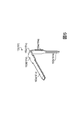
- FIG. FIG. 10 is a U-U ′ sectional view of FIG. 9.
- FIG. 11B is a sectional view taken along the line T-T ′ of FIG. 11A. The enlarged view of the area
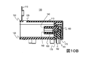
- FIG. 11B The perspective view which shows the right side surface, back surface, and bottom surface of the connector 100 of the state which has not attached the outer side shield case 110.
- FIG. 11B The perspective view which shows the right side surface, back surface, and bottom surface of the connector 100 of the state which has
- FIG. 2 shows the connector 100 according to the first embodiment.
- the connector 100 includes an outer shield case 110, a case 120, and a connector member 130.
- the connector member 130 includes a body 140, a plurality of contacts, an inner shield cover 160, and a spacer 170.
- resin springs 120g, 120h, 120i, and 120j are formed in the case 120.
- the inner shield cover 160 included in the connector member 130 is formed with locking portions 130g, 130h, 130i, and 130j having a press working fracture surface. Fixing claws that increase in thickness inward from the rear to the front are integrally formed at the free ends of the resin springs 120g, 120h, 120i, and 120j of the case 120. Therefore, when the connector member 130 is inserted into the case 120 from behind the case 120, the resin springs 120g, 120h, 120i, and 120j are elastically pushed outward and the connector member 130 enters a predetermined position. Restore later.
- the fixing claw is engaged with the engaging portions 130g, 130h, 130i, and 130j of the inner shield cover 160. Details of each part will be described below.
- the surface into which the mating plug-type connector is inserted is the front surface of the connector 100, the surface that becomes the mounting surface when mounted on the board is the bottom surface, and the front direction when viewed from the center of the connector 100 Is assumed to be the front and the bottom direction is the lower side.
- the body 140 is made of an insulator and has a substantially rectangular box shape.
- the body 140 has an insertion port 140a, an insertion space 140b, and a plurality of holes 140e (see FIG. 4B).
- the insertion port 140a is formed in front of the body 140 so that the mating plug-type connector can be inserted.
- the insertion space 140b is formed to extend from the insertion port 140a toward the rear wall 140f.
- the plurality of holes 140e are formed in the rear wall 140f so as to penetrate the plurality of contacts, respectively.
- a hole 140e for an upper contact 151 described later is indicated by a broken line.
- Contacts described later are disposed on the upper wall surface and the lower wall surface of the inner circumferential surface of the insertion space 140b of the body 140.
- a plurality of contact portion grooves 140 c respectively corresponding to a plurality of lower contacts 152 described later are formed on the lower wall surface of the inner peripheral surface of the body 140.
- Each contact portion groove 140c extends from the insertion port 140a to the rear wall 140f in parallel with each other at regular intervals, and communicates with each hole 140e.
- the plurality of contacts are one or more upper contacts 151 arranged on the upper wall surface of the inner circumferential surface of the insertion space of the body 140, and one or more contacts arranged on the lower wall surface of the inner circumferential surface of the insertion space of the body 140.
- Lower contact 152 (see FIG. 3).
- the upper contact 151 and the lower contact 152 are made of a plate-shaped conductor. Although the length of each part is different, they have the same structure, and are also shown in FIG.
- the lower contact 152 includes a contact portion 152a, a first terminal portion 152b, and a body portion 152c.
- the contact part 152a contacts the contact of the mating plug type connector.
- the first terminal portion 152b serves as a terminal for the substrate when mounted on the substrate.
- the body portion 152c connects the contact portion 152a and the first terminal portion 152b. Further, the body portion 152c includes a press-fit portion 152d connected to the contact portion 152a and a guide portion 152e connected to the first terminal portion 152b.
- the upper contact 151 is similarly composed of 151a, 151b, 151c, 151d, and 151e.
- the contact portions 151a and 152a of the plurality of contacts 151 and 152 are arranged in contact portion grooves 140c formed on the upper wall surface and the lower wall surface of the inner peripheral surface of the insertion space 140b of the body 140, respectively.
- the contact portion 152a of the lower contact 152 is press-fitted from the rear of the body 140 through the hole 140e (see FIG. 4B) toward the front (in the direction of the arrow R in FIG. 4C) (see FIG. 4C, but the description). For this reason, the lower contact 152 at the right end is indicated by a broken line).
- the press-fit portion 152d is formed so that its width increases from the front to the rear (see FIG. 5). By adopting such a shape, it is possible to prevent the lower contact 152 from falling backward after the press-fit portion 152d is press-fitted into the hole 140e and the lower contact 152 is inserted into the body 140.
- the contact portion 152a is disposed in the contact portion groove 140c. The same applies to the upper wall surface of the inner peripheral surface of the body 140 and the upper contact 151.
- the body portion 152c is bent in the mounting surface direction (the direction of the arrow V in FIG. 3) behind the body 140. Furthermore, the first terminal portions 152 b of the lower contacts 152 arranged as shown in FIGS. 6A and 6B are guided to a predetermined position by the spacer 170.
- the guide portion 152e of the lower contact 152 has a portion formed such that its width decreases from the upper side to the lower side (FIG. 5).
- a flat plate-shaped hole 170b is formed in the spacer 170 (see FIG. 6B, but the lower contact 152 at the right end of the lower stage is not shown for explanation).
- the hole 170b is formed so that its width decreases from the upper side to the lower side and is in contact with the first terminal portion 152b at the end.
- the inner shield cover 160 includes a cover portion 160a, a second terminal portion 160b, and locking portions 130g, 130h, 130i, and 130j.
- Cover portion 160 a covers the outer peripheral surface of body 140.
- the two second terminal portions 160b serve as terminals for the substrate when mounted on the substrate.
- the locking portions 130g, 130h, 130i, and 130j are formed at the rear end. This rear end consists of a press-work fracture surface.
- the inner shield cover 160 is bent at the rear end of the body 140 in a direction perpendicular to the insertion direction of the mating plug-type connector and in the mounting surface direction. That is, in FIG. 3, it is bent 90 degrees in the direction of the arrow V along the broken line portion 160d.
- the inner shield cover 160 is formed by pressing from a conductor, for example, a metal plate. At this time, the long holes 160l, 160m, 160n, 160f and the like that become the locking portions 130g, 130h, 130i, and 130j are formed in the same manner.
- the inner shield cover 160 is separated from the metal plate by placing the metal plate as a material on the die of the mold and pushing the punch. Therefore, a fracture surface with a sharp edge is formed at the separation portion from the metal plate.
- the separated inner shield cover 160 is bent at a predetermined position, and is formed in a rectangular cylindrical shape having both side surfaces, an upper surface, and a bottom surface as shown in FIG.
- the rear portion of the inner shield cover 160 is aligned with the mating plug-type connector insertion direction along the upper rear end of the body 140. 7 and is bent in the mounting surface direction (the direction of arrow V in FIG. 3) to form the shape shown in FIG.
- the spacer 170 is made of an insulator and includes a plurality of holes 170b corresponding to the plurality of first terminal portions and two holes 170c corresponding to the two second terminal portions 160b. It is formed to provide.
- the holes 170b and 170c penetrate the spacer 170 in the vertical direction.
- locking part 130f is formed by penetrating and forming the hole 170c in the board part protruded in the horizontal direction.
- the holes 170b and 170c respectively bring the first terminal portion and the second terminal portion 160b to predetermined positions.
- the spacer 170 keeps a distance so that the upper contact 151, the lower contact 152, and the inner shield cover 160 do not contact each other.
- the connector member 130 includes the body 140, the plurality of contacts 151 and 152, the inner shield cover 160, and the spacer 170 (see FIG. 3).
- the body 140 is inserted into a rectangular tube portion formed by the cover portion 160a of the inner shield cover 160. Further, a contact is press-fitted into the body 140 from the rear.
- the body portions 151c and 152c of the contacts 151 and 152 are bent in a direction indicated by an arrow V in FIG. 3 (a direction perpendicular to the insertion direction and a mounting surface direction).
- the spacer 170 has the first terminal portions 151b and 152b of the contacts 151 and 152 and the second terminal portion 160b of the inner shield cover 160 inserted from above to place the first terminal portion and the second terminal portion 160b in a predetermined position. Deploy. Finally, the inner shield cover 160 is bent in the direction of arrow V in FIG. 3 at the rear end of the body 130, and the connector member 130 is assembled (see FIG. 2).
- a plurality of flanges 140k are formed at the front end of the body 140 so as to protrude from the outer periphery.
- a plurality of convex portions 160k projecting forward corresponding to the concave portions formed between the plurality of flange portions 140k are formed.
- two grooves 140l are formed on the upper surface of the body 140 from the front end toward the rear. The groove 140l is not formed up to the rear end of the body 140, and has an end portion on the upper surface of the body 140.
- two cut-and-raised portions 160l cut and raised downward are formed on the upper surface of the body 140.
- the flange portion 140k and the convex portion 160k are engaged with each other.
- the body 140 and the inner shield cover 160 are fixed in the vertical direction and the horizontal direction.
- the cut-and-raised portion 160l is elastically pushed outward (upward).
- the cut and raised portion 160l reaches the groove 140l on the upper surface of the body 140, the cut and raised portion 160l is restored.
- the flange 140k provided at the front end of the body 140 is engaged with the front end of the inner shield cover 160, and the end of the groove 140l provided on the upper surface of the body 140 and the cut-and-raised portion 160l of the inner shield cover are formed.
- the body 140 and the inner shield cover 160 are fixed in the front-rear direction.
- a fitting hole 160 f is formed above the second terminal portion 160 b of the inner shield cover 160.
- a protrusion 170f is formed on the inner peripheral surface of the hole 170c of the spacer 170 so as to increase in thickness from the top to the bottom (see FIG. 6B).
- a cut-and-raised portion 160m is formed on the side surface of the cover portion 160a of the inner shield cover 160, and a hole 160n is formed on the rear side surface.
- the cut-and-raised part 160m and the hole 160n are fitted. With such a structure, the inner shield cover 160 is fixed to the shape shown in FIG.
- the case 120 is an insulator and is formed in a rectangular cylindrical shape. In the case 120, openings 120e and 120d are formed so as to communicate with each other.
- the opening 120e is formed in front of the case 120 so as to be an insertion port for the mating plug-type connector (see FIG. 8).
- the opening 120d is formed behind the case 120 so as to serve as an insertion port for the connector member 130 (see FIG. 2).
- the case 120 is formed so that a part of the inner peripheral surface covers the outer peripheral surface of the connector member 130.
- the case 120 is integrally formed with resin springs 120g, 120h, 120i and 120j and fixed claws 120g ′, 120h ′, 120i ′ and 120j ′. ing.
- the resin springs 120g, 120h, 120i, and 120j are arranged inside the cylinder and extend rearward.
- the fixing claws 120g ', 120h', 120i 'and 120j' are arranged at the free ends of the resin springs and increase in thickness from the rear toward the front.
- a slit 120f is formed under the resin springs 120g and 120j on the inner peripheral surface of the case (see FIG. 2).
- the peripheral edge of the front surface of the connector member 130 is fixed to the fixing claws 120g ′, 120i ′, and 120j ′ of the case 120.
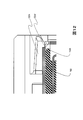
- the resin springs 120g, 120h, 120i, and 120j of the case 120 are elastically pushed outward. After the connector member 130 enters the predetermined position, the resin springs 120g, 120h, 120i, and 120j are restored (see FIGS. 11A, 11B, 12, and 13).
- the predetermined position means that the connector member 130 is inserted until, for example, the fixing claws 120g ′, 120h ′, 120i ′, and 120j ′ reach the locking portions 130g, 130h, 130i, and 130j of the inner shield cover 160, respectively. It is the position when.
- the fixing claws 120g ', 120h', 120i 'and 120j' are locked to the locking portions 130g, 130h, 130i and 130j of the inner shield cover 160 (see FIG. 12).
- locking part 130f formed in the spacer 170 which comprises the connector member 130 is inserted in the slit 120f (refer FIG. 2).
- the front edge of the locking portion 130f comes into contact with the end portion formed by the slit 120f.
- the connector member 130 can be fixed to the case 120 in the front-rear, up-down, left-right directions. That is, the back surface of the case 120, the slit 120f, the fixing claws 120g ′, 120h ′, 120i ′, and 120j ′, the front surface of the connector member 130, the locking portion 130f, and the locking portions 130g, 130h, 130i, and 130j,
- the connector member 130 is fixed to the case 120 in the front-rear direction. Further, the connector member 130 is fixed to the case 120 in the vertical and horizontal directions by the inner peripheral surface of the case 120 and the outer peripheral surface of the connector member 130.
- the press working fracture surface is substantially flat, it is possible to reduce the allowance for the fixed claws 120g ', 120h', 120i 'and 120j'.
- the bent portion is bent at the curvature radius. Therefore, it is necessary to increase the hooking cost as compared with the case where the fixed claw is hung on a flat press-processed fracture surface. Further, the bent portion tends to vary in the bending position and bending angle.
- the outer shield case 110 is a conductor and is formed in a rectangular box shape.
- the outer shield case 110 covers the outer peripheral surface of the case 120 except for the front and bottom surfaces of the case 120.
- a plurality of step portions 110b and a plurality of third terminal portions 110a are formed on both side surfaces of the outer shield case 110.
- the step portion 110b is bent inward and is bent downward in parallel with the side surface.
- the third terminal portion 110a extends further downward from the stepped portion 110.
- the third terminal portion 110a slides downward in guide grooves 120a provided in the vertical direction on both side surfaces of the case 120, and the step portion 110b and the support portion 120b are locked.
- the third terminal portion 110a is fitted in the guide groove 120a, and the outer shield case 110 is fixed to the case 120 in the front-rear direction. Further, the third terminal portion 110 a and the support portion 120 b are engaged, and the outer shield case 110 is fixed in the left-right direction with respect to the case 120.
- the locking claw 110c of the outer shield case 110 is bent inward.
- the latching claw 110c and the latching portion 120c of the case 120 are engaged to complete the assembly.
- the outer shield case 110 is fixed to the case 120 in the vertical direction.
- the connector 100 is mounted on the substrate 210 of the electronic device 200.
- the substrate 210 of the electronic device 200 penetrates the first through hole 210a that penetrates through the first terminal portions 151b and 152b, the second through hole 210b that penetrates through the second terminal portion 160b, and the third terminal portion 110a.
- a third through hole 210c to be formed and a printed wiring are formed.
- Each through hole is provided at least as many as the corresponding terminal portions.
- the first terminal portions 151b and 152b and the second terminal portion 160b are respectively soldered to the substrate 210, and the connector 100 is fixed to the substrate 210 in the front and rear, right and left directions.
- the second terminal portion 160b and the third terminal portion 110a are grounded via the second through hole 210b and the third through hole 210c, respectively.
- the first terminal portions 151b and 152b are connected to each wiring through the first through hole 210a.
- a protrusion 120p is formed on the front bottom surface of the case 120 (see FIG. 10A).
- the substrate 210 is formed with a fourth through hole 210d that penetrates the protruding portion 120p (see FIG. 8).
- the outer shield case 110 includes a flange 110d extending upward at the front end.
- the flange 110d may be configured to include a screw hole 110e at the center thereof.
- the connector 100 can be fastened to the housing of the electronic device 200 (not shown) with a screw.
- the outer shield case 100 is grounded to a housing (not shown) via a flange 110d.
- the mating plug-type connector includes a flat plate insulating plate, and a plurality of upper and lower terminals, which are elongated conductive contact pieces, are provided on a plane on both plate surfaces. Even in the case of a structure having connecting portions arranged in parallel to each other, the contact portion with the mating plug-type connector can be covered with the inner shield cover 160. Therefore, the connector 100 can maintain a high shielding effect.
- the fixing claw of the case 120 and the locking portion having the press working fracture surface of the inner shield cover 160 are locked, and the position of the included connector member 130 is fixed. Therefore, it is not necessary to provide a large cut and a large hole in the inner shield, and it is not necessary to expose the body 140.
- the rear end is opened to allow the upper terminal and the lower terminal to pass through, but the inner shield cover 160 of the connector 100 covers the entire contact from the outside. Therefore, the inner shield cover 160 does not need such an opening at the rear end, and the shielding effect is enhanced.
- the resin spring and the fixing claw provided on the case 120 may be provided on at least one of both sides of the inner peripheral surface of the case 120, and may be provided on at least one of the upper and lower surfaces of the inner peripheral surface.
- a locking portion may be provided in at least a corresponding portion of the connector member 130.
Landscapes
- Details Of Connecting Devices For Male And Female Coupling (AREA)
- Coupling Device And Connection With Printed Circuit (AREA)
Abstract
Description
[第一実施形態]
図2は、第一実施形態に係るコネクタ100を示す。図2に示すように、コネクタ100は、外側シールドケース110と、ケース120と、コネクタ部材130とを有する。さらに、図3に示すように、コネクタ部材130は、ボディ140と、複数のコンタクトと、内側シールドカバー160と、スペーサ170とを備える。
図4A~図4Cに示すようにボディ140は、絶縁体からなり、略矩形箱状である。ボディ140には、挿入口140aと挿入空間140bと複数の孔140eとが形成されている(図4B参照)。挿入口140aは、ボディ140の前方に、相手側のプラグ型コネクタが挿入できるように形成されている。挿入空間140bは、挿入口140aから後方壁140fに向かって伸びるように形成されている。複数の孔140eは、後方壁140fに、それぞれ複数のコンタクトを貫通させるために形成されている。なお、図4B中、後述する上側コンタクト151用の孔140eを破線で示す。
ボディ140の挿入空間140bの内周面の上側壁面と下側壁面には、後述するコンタクトが配される。例えば、図4Cに示すように、ボディ140の内周面の下側壁面には、後述する複数の下側コンタクト152にそれぞれ対応する複数の接触部用溝140cが形成されている。各接触部用溝140cは、一定間隔で互いに平行に挿入口140aから後方壁140fまで延びており、各孔140eと連通している。
複数のコンタクトは、ボディ140の挿入空間の内周面の上側壁面に配される一本以上の上側コンタクト151と、ボディ140の挿入空間の内周面の下側壁面に配される一本以上の下側コンタクト152とからなる(図3参照)。上側コンタクト151及び下側コンタクト152は、平板形状の導電体からなる。これらは各部の長さが異なるが、同様の構造であり、図5を兼用して示す。下側コンタクト152は、接触部152aと第1端子部152bと胴体部152cとを含む。接触部152aは、相手側のプラグ型コネクタのコンタクトに接触する。第1端子部152bは、基板に実装される際に基板に対する端子となる。胴体部152cは、接触部152aと第1端子部152bとを接続する。さらに、胴体部152cは、接触部152aに接続する圧入部152dと第1端子部152bに接続するガイド部152eとからなる。なお、図5中、括弧内に示すように、上側コンタクト151も同様に151a、151b、151c、151d、151eから構成されている。
図2及び図7に示すように内側シールドカバー160は、カバー部160aと、第2端子部160bと、係止部130g、130h、130i及び130jとを含む。カバー部160aは、ボディ140の外周面を覆う。2つの第2端子部160bは、基板に実装される際に基板に対する端子となる。係止部130g、130h、130i及び130jは、後方端に形成されている。この後方端はプレス加工破断面からなる。
図6A及び図6Bに示すように、スペーサ170は、絶縁体からなり、複数の第1端子部に対応する複数の孔170bと、2つの第2端子部160bに対応する2つの孔170cとを備えるように形成されている。なお、孔170bと170cは上下方向にスペーサ170を貫通する。なお、横方向に突出した板部に孔170cを貫通形成することにより、係止部130fが形成されている。そして、スペーサ170の上方から下方に向かって第1端子部と第2端子部160bを挿入するときに、孔170b及び170cは、それぞれ第1端子部と第2端子部160bを、所定の位置にガイドする。このようにして、スペーサ170は、上側コンタクト151と下側コンタクト152と内側シールドカバー160とが接触しないように間隔を保持する。
前述の通り、コネクタ部材130は、ボディ140と、複数のコンタクト151、152と、内側シールドカバー160と、スペーサ170とを備える(図3参照)。まず、内側シールドカバー160のカバー部160aの成す角筒部分に、ボディ140が挿入される。さらに、ボディ140に、その後方からコンタクトが圧入される。コンタクト151、152の胴体部151c、152cは、図3の矢印Vの方向(挿入方向と垂直方向であって、かつ、実装面方向)に折り曲げられる。スペーサ170は、その上方からコンタクト151、152の第1端子部151b、152bと内側シールドカバー160の第2端子部160bを挿入され、第1端子部と第2端子部160bとを所定の位置に配置する。最後に、内側シールドカバー160は、ボディ130の後方端において、図3の矢印Vの方向に折り曲げられて、コネクタ部材130は組み立てられる(図2参照)。
ケース120は、絶縁体であり矩形筒状に形成されている。ケース120には、開口部120eと120dとが連通して形成されている。開口部120eは、ケース120の前方に相手側のプラグ型コネクタの挿入口となるように形成されている(図8参照)。開口部120dは、ケース120の後方にコネクタ部材130の挿入口となるように形成されている(図2参照)。
図2、図10A及び図10Bに示すように外側シールドケース110は、導体であり、矩形箱状に形成されている。外側シールドケース110は、ケース120の正面及び底面を除くケース120の外周面を覆う。外側シールドケース110の両側面には、複数の段差部110bと複数の第3端子部110aとが形成されている。段差部110bは、内側に折れ曲げられ、側面と平行に下方に向かって折れ曲げられる。第3端子部110aは、段差部110からさらに下方に伸びる。第3端子部110aは、ケース120の両側面に上下方向に設けられたガイド溝120aを下方に向かってスライドし、段差部110bと支持部120bとが係止する。第3端子部110aがガイド溝120aに嵌合し、外側シールドケース110はケース120に対して前後方向に固定される。また、第3端子部110aと支持部120bとが係合し、外側シールドケース110はケース120に対して左右方向に固定される。
図8に示すように電子機器200の基板210上には、コネクタ100が実装されている。電子機器200の基板210には、第1端子部151b、152bに貫通される第1貫通孔210aと、第2端子部160bに貫通される第2貫通孔210bと、第3端子部110aに貫通される第3貫通孔210cと、プリント配線とが形成されている。各貫通孔は、少なくとも対応する端子部の数だけ設けられる。
このような構成とすることによって、相手側のプラグ型コネクタが、平板絶縁板を備え、その両板面に、それぞれ、細長い導電性接片である上側ターミナル及び下側ターミナルを平面上に複数個互いに平行に配列された接続部を備えた構造となっている場合であっても、相手側のプラグ型コネクタとの接触部分を内側シールドカバー160で覆うことができる。そのため、コネクタ100は高いシールド効果を保持できる。ケース120の固定爪と内側シールドカバー160のプレス加工破断面を有する係止部とが係止し、内包されるコネクタ部材130の位置が固定される。そのため、大きな切り起こしや大きな孔を内側シールドに設けずともよく、ボディ140を露出させる必要がない。また、特許文献1の内側シールドケース3の場合には、上側ターミナル及び下側ターミナルを通すために、後方端は開口されているが、コネクタ100の内側シールドカバー160は、コンタクト全体を外側から覆うため、内側シールドカバー160にはそのような後方端の開口も必要なく、シールド効果が高くなる。
ケース120に設けられる樹脂バネ及び固定爪は、少なくともケース120の内周面の両側面の少なくとも何れかに1つ設け、内周面の上下面の少なくとも何れかに1つ設ければよく、そのとき、コネクタ部材130の少なくとも対応する部分に係止部を設ければよい。
コネクタ部材130を組み立てる際、コンタクトの胴体部分の曲げ加工後に、コンタクトをボディ140に圧入してもよい。
上述の本発明の実施形態の記載は、例証と記載の目的で提示されたものである。網羅的であるという意図はなく、開示された厳密な形式に発明を限定する意図もない。変形やバリエーションは上述の教示から可能である。実施形態は、本発明の原理を最も良い例証を提供するために、そして、その分野の当業者が、熟考された実際の使用に適するように本発明を色々な実施形態で、また、色々な変形を付加して利用できるようにするために、選ばれて表現されたものである。全てのそのような変形やバリエーションは、公正に合法的に公平に与えられる幅に従って解釈された添付の請求項によって定められた本発明の範囲内である。
Claims (4)
- コネクタ部材とケースとを有し、
前記コネクタ部材は、
絶縁体からなり、前方に相手側のプラグ型コネクタが挿入できるように挿入口が形成されて、挿入口から後方に向かって伸びるように挿入空間が形成されているボディと、
前記ボディの挿入空間の内周壁面に配列され、相手側のプラグ型コネクタのコンタクトに接触する接触部と、基板に実装される際に基板に対する端子となる第1端子部と、前記接触部と前記第1端子部とを接続する胴体部とを含む複数のコンタクトと、
前記ボディの外周面を覆うカバー部と、基板に実装される際に基板に対する端子となる第2端子部と、プレス加工破断面からなる後方端に形成されている係止部とを含む内側シールドカバーと、を備え、
前記ケースは、筒状の絶縁体からなり、内周面の一部が前記コネクタ部材の外周面を覆うように形成され、筒状内部に配され後方に向かって伸びている樹脂バネと、樹脂バネの自由端に配され後方から前方に向かって内側に厚みを増す固定爪とが形成され、
前記ケースの後方から前記コネクタ部材が挿入され、前記樹脂バネは弾性的に外側に押し広げられ、前記固定爪が前記係止部に達するまで前記コネクタ部材が挿入されると、前記樹脂バネが復元して、前記固定爪が前記内側シールドカバーの係止部に係止する、
ことを特徴とするコネクタ。 - 請求項1記載のコネクタであって、
前記コネクタ部材は、
絶縁体からなり、前記コンタクトと前記内側シールドカバーとが接触しないように間隔を保持するスペーサをさらに備え、
前記コンタクトは前記ボディに圧入され、前記胴体部は前記ボディ後方において実装面方向に曲げられ、前記第1端子部は前記スペーサにより所定の位置にガイドされ、前記内側シールドカバーはボディ後方端において相手側のプラグ型コネクタの挿入方向と垂直方向であって、かつ、実装面方向に曲げられている、
ことを特徴とするコネクタ。 - 請求項1または請求項2記載のコネクタであって、
前記ケースの外周面を覆う外側シールドケースを備える、
ことを特徴とするコネクタ。 - 請求項1から請求項3の何れかに記載のコネクタを備える電子機器であって、
前記コネクタを基板上に実装している、
ことを特徴とする電子機器。
Priority Applications (6)
| Application Number | Priority Date | Filing Date | Title |
|---|---|---|---|
| KR1020137005891A KR101729720B1 (ko) | 2010-09-28 | 2011-09-27 | 커넥터 및 전자기기 |
| MX2013003172A MX2013003172A (es) | 2010-09-28 | 2011-09-27 | Conector y dispositivo electronico. |
| US13/819,381 US9004945B2 (en) | 2010-09-28 | 2011-09-27 | Connector and electronic device |
| CN201180046746.0A CN103140993B (zh) | 2010-09-28 | 2011-09-27 | 连接器及电子设备 |
| EP11829095.6A EP2624374B1 (en) | 2010-09-28 | 2011-09-27 | Connector and electronic device |
| CA2809935A CA2809935C (en) | 2010-09-28 | 2011-09-27 | Connector and electronic device |
Applications Claiming Priority (2)
| Application Number | Priority Date | Filing Date | Title |
|---|---|---|---|
| JP2010217669A JP5524009B2 (ja) | 2010-09-28 | 2010-09-28 | コネクタ及び電子機器 |
| JP2010-217669 | 2010-09-28 |
Publications (1)
| Publication Number | Publication Date |
|---|---|
| WO2012043542A1 true WO2012043542A1 (ja) | 2012-04-05 |
Family
ID=45892982
Family Applications (1)
| Application Number | Title | Priority Date | Filing Date |
|---|---|---|---|
| PCT/JP2011/072038 Ceased WO2012043542A1 (ja) | 2010-09-28 | 2011-09-27 | コネクタ及び電子機器 |
Country Status (9)
| Country | Link |
|---|---|
| US (1) | US9004945B2 (ja) |
| EP (1) | EP2624374B1 (ja) |
| JP (1) | JP5524009B2 (ja) |
| KR (1) | KR101729720B1 (ja) |
| CN (1) | CN103140993B (ja) |
| CA (1) | CA2809935C (ja) |
| MX (1) | MX2013003172A (ja) |
| TW (1) | TWI530034B (ja) |
| WO (1) | WO2012043542A1 (ja) |
Cited By (1)
| Publication number | Priority date | Publication date | Assignee | Title |
|---|---|---|---|---|
| CN103427209A (zh) * | 2012-07-19 | 2013-12-04 | 深圳市长盈精密技术股份有限公司 | 电子卡连接器 |
Families Citing this family (27)
| Publication number | Priority date | Publication date | Assignee | Title |
|---|---|---|---|---|
| JP5822328B2 (ja) * | 2010-08-31 | 2015-11-24 | 矢崎総業株式会社 | 基板搭載型コネクタ |
| JP5524009B2 (ja) * | 2010-09-28 | 2014-06-18 | ホシデン株式会社 | コネクタ及び電子機器 |
| CN202422141U (zh) * | 2011-11-21 | 2012-09-05 | 深圳市新国都技术股份有限公司 | Ic卡读取设备及其ic卡座保护件 |
| JP5392931B1 (ja) | 2012-09-14 | 2014-01-22 | 日本航空電子工業株式会社 | コネクタ |
| CN203367606U (zh) * | 2013-06-18 | 2013-12-25 | 富士康(昆山)电脑接插件有限公司 | 电连接器 |
| JP6150053B2 (ja) * | 2013-07-02 | 2017-06-21 | Smk株式会社 | コネクタ |
| US9099814B2 (en) * | 2013-07-16 | 2015-08-04 | Delphi Technologies, Inc. | Shielded electrical header assembly |
| JP6078919B2 (ja) * | 2013-07-18 | 2017-02-15 | ホシデン株式会社 | コネクタ |
| US9912111B2 (en) * | 2013-07-19 | 2018-03-06 | Foxconn Interconnect Technology Limited | Flippable electrical connector |
| US8974252B1 (en) * | 2013-09-04 | 2015-03-10 | Cheng Uei Precision Industry Co., Ltd. | Electrical connector |
| JP6319657B2 (ja) * | 2014-05-14 | 2018-05-09 | Smk株式会社 | シールドコネクタ |
| KR101583934B1 (ko) * | 2014-05-26 | 2016-01-08 | 현대자동차주식회사 | 차폐형 커넥터 |
| WO2015196913A1 (zh) * | 2014-06-27 | 2015-12-30 | 深圳市得润电子股份有限公司 | 一种线缆连接器组件、板端连接器组件及其电连接器组合 |
| KR102093434B1 (ko) * | 2015-01-08 | 2020-03-25 | 엘에스엠트론 주식회사 | 리셉터클 커넥터 |
| JP6311937B2 (ja) * | 2015-02-12 | 2018-04-18 | 株式会社オートネットワーク技術研究所 | コネクタ及びシールドシェル |
| JP6160844B2 (ja) * | 2015-04-08 | 2017-07-12 | Smk株式会社 | コネクタ |
| WO2016179748A1 (zh) * | 2015-05-08 | 2016-11-17 | 华为技术有限公司 | 一种光纤终端盒 |
| US9425558B1 (en) * | 2015-10-22 | 2016-08-23 | Cheng Uei Precision Industry Co., Ltd. | Electrical connector having an outer shielding covered by a cover with a resilient plate extending upward and rearward |
| JP6534917B2 (ja) * | 2015-11-26 | 2019-06-26 | 日本圧着端子製造株式会社 | シールドコネクタ |
| JP6819778B2 (ja) | 2017-05-18 | 2021-01-27 | 株式会社村田製作所 | 携帯型電子機器 |
| USD831572S1 (en) * | 2017-11-20 | 2018-10-23 | The Charles Machine Works, Inc. | Electrical connection cover |
| CN109935996B (zh) * | 2017-12-15 | 2022-01-25 | 富士康(昆山)电脑接插件有限公司 | 滑轨连接器 |
| JP7432990B2 (ja) * | 2018-11-13 | 2024-02-19 | タイコエレクトロニクスジャパン合同会社 | 電気機器 |
| CN110474202A (zh) * | 2019-07-25 | 2019-11-19 | 深圳市亚力盛电子股份有限公司 | 连接器母座和连接器 |
| JP7387407B2 (ja) * | 2019-11-27 | 2023-11-28 | 日本航空電子工業株式会社 | コネクタ組立体 |
| JP2022018327A (ja) * | 2020-07-15 | 2022-01-27 | ホシデン株式会社 | コネクタ |
| CN220253526U (zh) * | 2023-07-14 | 2023-12-26 | 智邦科技股份有限公司 | 具有屏蔽结构的卡缘连接器及屏蔽件 |
Citations (4)
| Publication number | Priority date | Publication date | Assignee | Title |
|---|---|---|---|---|
| JPH02150682U (ja) * | 1989-05-22 | 1990-12-27 | ||
| JPH08106961A (ja) | 1994-10-04 | 1996-04-23 | Smk Corp | 2重シールドコネクタ |
| JP2009193858A (ja) * | 2008-02-15 | 2009-08-27 | Yazaki Corp | シールドコネクタ |
| JP2011060613A (ja) * | 2009-09-10 | 2011-03-24 | Japan Aviation Electronics Industry Ltd | コネクタ組立体 |
Family Cites Families (13)
| Publication number | Priority date | Publication date | Assignee | Title |
|---|---|---|---|---|
| JPH02150682A (ja) | 1988-12-02 | 1990-06-08 | Mitsubishi Electric Corp | 冷蔵庫 |
| TW323011U (en) * | 1997-02-18 | 1997-12-11 | Hon Hai Prec Ind Co Ltd | Connector of telecommunication slot |
| US6368155B1 (en) | 1999-07-16 | 2002-04-09 | Molex Incorporated | Intelligent sensing connectors |
| TW517898U (en) * | 2001-12-21 | 2003-01-11 | Hon Hai Prec Ind Co Ltd | Combinational connector |
| US6659806B2 (en) * | 2001-12-26 | 2003-12-09 | Hon Hai Precision Ind.? Co., Ltd. | Modular jack connector |
| US6609929B2 (en) * | 2002-01-18 | 2003-08-26 | Molex Incorporated | Electrical connector assembly |
| TW549740U (en) * | 2002-07-26 | 2003-08-21 | Hon Hai Prec Ind Co Ltd | Electrical connector |
| US6743047B2 (en) * | 2002-10-23 | 2004-06-01 | Hon Hai Precision Ind. Co., Ltd. | Electrical connector with rear ground plate |
| TW555209U (en) * | 2002-12-24 | 2003-09-21 | Molex Taiwan Ltd | Electrical connector |
| JP4232037B2 (ja) * | 2004-08-09 | 2009-03-04 | ヒロセ電機株式会社 | シールドコネクタ |
| US7967631B2 (en) * | 2008-06-06 | 2011-06-28 | Hon Hai Precision Ind. Co., Ltd. | Stacked electrical connector with improved insulators |
| CN201230038Y (zh) * | 2008-06-06 | 2009-04-29 | 富士康(昆山)电脑接插件有限公司 | 电连接器 |
| JP5524009B2 (ja) * | 2010-09-28 | 2014-06-18 | ホシデン株式会社 | コネクタ及び電子機器 |
-
2010
- 2010-09-28 JP JP2010217669A patent/JP5524009B2/ja active Active
-
2011
- 2011-08-31 TW TW100131297A patent/TWI530034B/zh active
- 2011-09-27 WO PCT/JP2011/072038 patent/WO2012043542A1/ja not_active Ceased
- 2011-09-27 KR KR1020137005891A patent/KR101729720B1/ko active Active
- 2011-09-27 CA CA2809935A patent/CA2809935C/en active Active
- 2011-09-27 US US13/819,381 patent/US9004945B2/en active Active
- 2011-09-27 MX MX2013003172A patent/MX2013003172A/es active IP Right Grant
- 2011-09-27 CN CN201180046746.0A patent/CN103140993B/zh active Active
- 2011-09-27 EP EP11829095.6A patent/EP2624374B1/en active Active
Patent Citations (4)
| Publication number | Priority date | Publication date | Assignee | Title |
|---|---|---|---|---|
| JPH02150682U (ja) * | 1989-05-22 | 1990-12-27 | ||
| JPH08106961A (ja) | 1994-10-04 | 1996-04-23 | Smk Corp | 2重シールドコネクタ |
| JP2009193858A (ja) * | 2008-02-15 | 2009-08-27 | Yazaki Corp | シールドコネクタ |
| JP2011060613A (ja) * | 2009-09-10 | 2011-03-24 | Japan Aviation Electronics Industry Ltd | コネクタ組立体 |
Non-Patent Citations (1)
| Title |
|---|
| See also references of EP2624374A4 |
Cited By (1)
| Publication number | Priority date | Publication date | Assignee | Title |
|---|---|---|---|---|
| CN103427209A (zh) * | 2012-07-19 | 2013-12-04 | 深圳市长盈精密技术股份有限公司 | 电子卡连接器 |
Also Published As
| Publication number | Publication date |
|---|---|
| CN103140993B (zh) | 2015-11-25 |
| US9004945B2 (en) | 2015-04-14 |
| CA2809935C (en) | 2017-10-31 |
| JP5524009B2 (ja) | 2014-06-18 |
| EP2624374A1 (en) | 2013-08-07 |
| EP2624374B1 (en) | 2016-11-16 |
| MX2013003172A (es) | 2013-07-29 |
| TW201230548A (en) | 2012-07-16 |
| TWI530034B (zh) | 2016-04-11 |
| KR101729720B1 (ko) | 2017-04-24 |
| KR20130113431A (ko) | 2013-10-15 |
| CN103140993A (zh) | 2013-06-05 |
| US20130178100A1 (en) | 2013-07-11 |
| CA2809935A1 (en) | 2012-04-05 |
| JP2012074223A (ja) | 2012-04-12 |
| EP2624374A4 (en) | 2014-04-02 |
Similar Documents
| Publication | Publication Date | Title |
|---|---|---|
| WO2012043542A1 (ja) | コネクタ及び電子機器 | |
| US9312641B2 (en) | Electrical connector used for transmitting high frequency signals | |
| US9502827B2 (en) | Electrical connector with improved metal shell | |
| JP6222751B2 (ja) | ヘッダーアセンブリ | |
| US9356406B2 (en) | Electrical connector | |
| US7134900B2 (en) | Electrical connector assembly with multi-function latching member | |
| US8905781B2 (en) | Coaxial electrical connector having retaining arms and coaxial electrical connector assembly having the same | |
| US9263836B2 (en) | Electrical connector reducing antenna interference | |
| US9509099B2 (en) | Electrical connector having improved anti-EMI performance | |
| US20100093215A1 (en) | Electrical connector having an improved spring member for abutting against a metal plate | |
| US20110143577A1 (en) | Cable connector assembly with a front shell | |
| JP6847016B2 (ja) | 同軸ケーブル用コネクタ | |
| US7410390B2 (en) | Electrical receptacle connector with shell | |
| US7618268B2 (en) | Electrical connector with reliable mating frame mating with another connector | |
| US11296450B2 (en) | Electrical connector assembly | |
| US7867010B1 (en) | Electrical connector having latchs for locking with a complementary connector | |
| US7241160B2 (en) | Shielded electrical connector for camera module | |
| US20150207269A1 (en) | Card connector with metallic retaining plate | |
| US20110183545A1 (en) | Electrical connector with metallic shell firmly retained with the insulative housing | |
| US7318753B2 (en) | Electrical jack with improved grounding contact | |
| US6547590B2 (en) | Electrical connector assembly having spacer for positioning terminals | |
| US20060079130A1 (en) | Power connector | |
| US9698527B2 (en) | Electrical connector having a metallic reinforcing member | |
| US7686648B2 (en) | Electrical connector having an improved housing |
Legal Events
| Date | Code | Title | Description |
|---|---|---|---|
| WWE | Wipo information: entry into national phase |
Ref document number: 201180046746.0 Country of ref document: CN |
|
| 121 | Ep: the epo has been informed by wipo that ep was designated in this application |
Ref document number: 11829095 Country of ref document: EP Kind code of ref document: A1 |
|
| WWE | Wipo information: entry into national phase |
Ref document number: 13819381 Country of ref document: US |
|
| ENP | Entry into the national phase |
Ref document number: 2809935 Country of ref document: CA |
|
| REEP | Request for entry into the european phase |
Ref document number: 2011829095 Country of ref document: EP |
|
| WWE | Wipo information: entry into national phase |
Ref document number: 2011829095 Country of ref document: EP |
|
| ENP | Entry into the national phase |
Ref document number: 20137005891 Country of ref document: KR Kind code of ref document: A |
|
| WWE | Wipo information: entry into national phase |
Ref document number: MX/A/2013/003172 Country of ref document: MX |
|
| NENP | Non-entry into the national phase |
Ref country code: DE |