WO2012060404A1 - 有機発光ダイオードおよびその製造方法、画像表示装置および照明装置 - Google Patents
有機発光ダイオードおよびその製造方法、画像表示装置および照明装置 Download PDFInfo
- Publication number
- WO2012060404A1 WO2012060404A1 PCT/JP2011/075285 JP2011075285W WO2012060404A1 WO 2012060404 A1 WO2012060404 A1 WO 2012060404A1 JP 2011075285 W JP2011075285 W JP 2011075285W WO 2012060404 A1 WO2012060404 A1 WO 2012060404A1
- Authority
- WO
- WIPO (PCT)
- Prior art keywords
- light emitting
- layer
- emitting diode
- organic light
- organic
- Prior art date
- Legal status (The legal status is an assumption and is not a legal conclusion. Google has not performed a legal analysis and makes no representation as to the accuracy of the status listed.)
- Ceased
Links
Images


Classifications
-
- H—ELECTRICITY
- H10—SEMICONDUCTOR DEVICES; ELECTRIC SOLID-STATE DEVICES NOT OTHERWISE PROVIDED FOR
- H10K—ORGANIC ELECTRIC SOLID-STATE DEVICES
- H10K50/00—Organic light-emitting devices
- H10K50/80—Constructional details
- H10K50/805—Electrodes
- H10K50/82—Cathodes
- H10K50/822—Cathodes characterised by their shape
-
- H—ELECTRICITY
- H10—SEMICONDUCTOR DEVICES; ELECTRIC SOLID-STATE DEVICES NOT OTHERWISE PROVIDED FOR
- H10K—ORGANIC ELECTRIC SOLID-STATE DEVICES
- H10K50/00—Organic light-emitting devices
- H10K50/80—Constructional details
- H10K50/805—Electrodes
-
- H—ELECTRICITY
- H10—SEMICONDUCTOR DEVICES; ELECTRIC SOLID-STATE DEVICES NOT OTHERWISE PROVIDED FOR
- H10K—ORGANIC ELECTRIC SOLID-STATE DEVICES
- H10K50/00—Organic light-emitting devices
- H10K50/80—Constructional details
- H10K50/805—Electrodes
- H10K50/81—Anodes
-
- H—ELECTRICITY
- H10—SEMICONDUCTOR DEVICES; ELECTRIC SOLID-STATE DEVICES NOT OTHERWISE PROVIDED FOR
- H10K—ORGANIC ELECTRIC SOLID-STATE DEVICES
- H10K50/00—Organic light-emitting devices
- H10K50/80—Constructional details
- H10K50/805—Electrodes
- H10K50/81—Anodes
- H10K50/816—Multilayers, e.g. transparent multilayers
-
- H—ELECTRICITY
- H10—SEMICONDUCTOR DEVICES; ELECTRIC SOLID-STATE DEVICES NOT OTHERWISE PROVIDED FOR
- H10K—ORGANIC ELECTRIC SOLID-STATE DEVICES
- H10K50/00—Organic light-emitting devices
- H10K50/80—Constructional details
- H10K50/805—Electrodes
- H10K50/82—Cathodes
-
- H—ELECTRICITY
- H10—SEMICONDUCTOR DEVICES; ELECTRIC SOLID-STATE DEVICES NOT OTHERWISE PROVIDED FOR
- H10K—ORGANIC ELECTRIC SOLID-STATE DEVICES
- H10K50/00—Organic light-emitting devices
- H10K50/80—Constructional details
- H10K50/85—Arrangements for extracting light from the devices
-
- H—ELECTRICITY
- H10—SEMICONDUCTOR DEVICES; ELECTRIC SOLID-STATE DEVICES NOT OTHERWISE PROVIDED FOR
- H10K—ORGANIC ELECTRIC SOLID-STATE DEVICES
- H10K50/00—Organic light-emitting devices
- H10K50/80—Constructional details
- H10K50/85—Arrangements for extracting light from the devices
- H10K50/854—Arrangements for extracting light from the devices comprising scattering means
-
- H—ELECTRICITY
- H10—SEMICONDUCTOR DEVICES; ELECTRIC SOLID-STATE DEVICES NOT OTHERWISE PROVIDED FOR
- H10K—ORGANIC ELECTRIC SOLID-STATE DEVICES
- H10K50/00—Organic light-emitting devices
- H10K50/80—Constructional details
- H10K50/85—Arrangements for extracting light from the devices
- H10K50/858—Arrangements for extracting light from the devices comprising refractive means, e.g. lenses
-
- H—ELECTRICITY
- H10—SEMICONDUCTOR DEVICES; ELECTRIC SOLID-STATE DEVICES NOT OTHERWISE PROVIDED FOR
- H10K—ORGANIC ELECTRIC SOLID-STATE DEVICES
- H10K59/00—Integrated devices, or assemblies of multiple devices, comprising at least one organic light-emitting element covered by group H10K50/00
- H10K59/30—Devices specially adapted for multicolour light emission
- H10K59/32—Stacked devices having two or more layers, each emitting at different wavelengths
-
- H—ELECTRICITY
- H10—SEMICONDUCTOR DEVICES; ELECTRIC SOLID-STATE DEVICES NOT OTHERWISE PROVIDED FOR
- H10K—ORGANIC ELECTRIC SOLID-STATE DEVICES
- H10K71/00—Manufacture or treatment specially adapted for the organic devices covered by this subclass
-
- H—ELECTRICITY
- H10—SEMICONDUCTOR DEVICES; ELECTRIC SOLID-STATE DEVICES NOT OTHERWISE PROVIDED FOR
- H10K—ORGANIC ELECTRIC SOLID-STATE DEVICES
- H10K71/00—Manufacture or treatment specially adapted for the organic devices covered by this subclass
- H10K71/60—Forming conductive regions or layers, e.g. electrodes
-
- H—ELECTRICITY
- H10—SEMICONDUCTOR DEVICES; ELECTRIC SOLID-STATE DEVICES NOT OTHERWISE PROVIDED FOR
- H10K—ORGANIC ELECTRIC SOLID-STATE DEVICES
- H10K77/00—Constructional details of devices covered by this subclass and not covered by groups H10K10/80, H10K30/80, H10K50/80 or H10K59/80
- H10K77/10—Substrates, e.g. flexible substrates
-
- H—ELECTRICITY
- H10—SEMICONDUCTOR DEVICES; ELECTRIC SOLID-STATE DEVICES NOT OTHERWISE PROVIDED FOR
- H10K—ORGANIC ELECTRIC SOLID-STATE DEVICES
- H10K50/00—Organic light-emitting devices
- H10K50/80—Constructional details
- H10K50/805—Electrodes
- H10K50/81—Anodes
- H10K50/813—Anodes characterised by their shape
Definitions
- the present invention relates to an organic light emitting diode and a method for manufacturing the same, and an image display device and an illumination device including the organic light emitting diode.
- An organic light emitting diode is a light emitting element using organic electroluminescence (hereinafter referred to as organic EL), and generally an anode and a cathode are provided on both sides of an organic EL layer including a light emitting layer containing an organic light emitting material. It has the structure which was made.
- As the organic EL layer an electron transport layer, a hole transport layer, and the like are provided as necessary in addition to the light emitting layer.
- an anode made of a transparent conductive material such as ITO, an organic EL layer including a light emitting layer, and a cathode made of metal are sequentially formed on a transparent substrate such as a glass substrate, and light is extracted from the substrate side.
- Organic light-emitting diodes have advantages such as low viewing angle dependency, low power consumption, and extremely thin layers, but also have low light extraction efficiency.
- the light extraction efficiency is the ratio of the light energy emitted from the light extraction surface (for example, the substrate surface in the case of the bottom emission type) to the atmosphere with respect to the light energy emitted from the light emitting layer.
- light emitted from the light-emitting layer is emitted in all directions, so that most of the light enters a waveguide mode in which total reflection is repeated at the interface between multiple layers with different refractive indexes.
- the light extraction efficiency decreases.
- the distance from the cathode, which is a metal is short, part of the near-field light from the light emitting layer is converted to surface plasmon on the surface of the cathode and lost, and the light extraction efficiency is lowered. Since the light extraction efficiency affects the brightness of a display, illumination, or the like provided with the organic light emitting diode, various methods have been studied for the improvement.
- Patent Documents 1 to 4 disclose a method of providing a one-dimensional or two-dimensional periodic microstructure on the surface of a metal layer (cathode).
- the periodic microstructure functions as a diffraction grating.
- JP 2002-270891 A JP 2004-31350 A JP 2005-535121 Gazette JP 2009-158478 A
- the present invention has been made in view of the above circumstances, and an object thereof is to provide an organic light emitting diode excellent in light extraction efficiency and a method for manufacturing the same, and an image display device and an illumination device including the organic light emitting diode. To do.
- the present invention has the following aspects. [1] On the substrate, at least an anode conductive layer, an organic EL layer including a light emitting layer containing an organic light emitting material, and a cathode conductive layer made of an alloy having an Ag or Ag content of 70% by mass or more are sequentially provided.
- the light extraction wavelength ⁇ (nm) of light from the organic light emitting diode and the distance p (nm) between the centers of the recesses in the two-dimensional grating structure are shown in the following coordinates A, B, C , D, E, F, G, H, I, J, A in an area surrounded by a straight line, and the depth of the recess is 12 nm or more and 180 nm or less, .
- a method for producing the organic light emitting diode according to [1] A substrate having a structure in which a plurality of convex portions corresponding to the two-dimensional lattice structure are periodically arranged in a two-dimensional manner is formed on the surface, and on the structure, the anode conductive layer, the organic EL layer, A method for producing an organic light emitting diode, comprising sequentially laminating the cathode conductive layer.
- [4] including producing the substrate using the two-dimensional lattice structure as a mold, The organic mold according to [2], wherein the mold is a master produced by a dry etching method using a particle monolayer film as an etching mask, or a metal electromold or a resin mold obtained by transferring the master. Manufacturing method of light emitting diode.
- the substrate On the substrate, at least a cathode conductive layer made of Ag or an alloy containing 70 mass% or more of Ag, an organic EL layer including a light emitting layer containing an organic light emitting material, and an anode conductive layer are sequentially formed.
- the light extraction wavelength ⁇ (nm) of light from the organic light emitting diode and the distance p (nm) between the centers of the recesses in the two-dimensional grating structure are shown in the following coordinates A, B, C , D, E, F, G, H, I, J, A in an area surrounded by a straight line, and the depth of the recess is 12 nm or more and 180 nm or less, .
- [7] including producing the substrate using the two-dimensional lattice structure as a mold; [6] The organic material according to [6], wherein the mold is a master produced by a dry etching method using a particle monolayer film as an etching mask, or a metal electromold or a resin mold obtained by transferring the master. Manufacturing method of light emitting diode. [8] After producing a particle single layer film on the surface of the substrate, a metal selected from the group consisting of Cr, Ni, Fe and Co is vacuum deposited on the particle single layer film to form the particle single layer.
- the particle monolayer film is removed, and dry etching using the mesh-like metal vapor deposition layer as an etching mask.
- an organic light-emitting diode which is sequentially stacked, and provided with a two-dimensional lattice structure in which a plurality of convex portions are periodically arranged in two dimensions on the surface of the cathode conductive layer on the organic electroluminescence layer side
- the light extraction wavelength ⁇ (nm) of light from the organic light emitting diode and the distance p (nm) between the centers of the convex portions in the two-dimensional lattice structure are represented by the following coordinates A, B
- the organic layer is located in a region surrounded by straight lines connecting C, D, E, F, G, H, I, J, and A sequentially, and the height of the convex portion is 12 nm or more and 180 nm or less.
- anode conductive layer On the substrate, at least an anode conductive layer, an organic electroluminescence layer including a light emitting layer containing an organic light emitting material, and a cathode conductive layer made of Al or an alloy having an Al content of 70% by mass or more.
- an organic light emitting diode which is sequentially laminated and provided with a two-dimensional lattice structure in which a plurality of concave portions are periodically arranged in two dimensions on the surface of the cathode conductive layer on the organic electroluminescence layer side
- the light extraction wavelength ⁇ (nm) of light from the organic light emitting diode and the distance p (nm) between the centers of the recesses in the two-dimensional lattice structure are represented by the following coordinates A ′, B ′ , C ′, D ′, E ′, F ′, G ′, H ′, I ′, J ′, K ′, L ′, and A ′ are in a region surrounded by a straight line, and the concave portion
- An organic light emitting diode having a depth of 12 nm to 180 nm.
- an organic light emitting diode which is sequentially laminated and provided with a two-dimensional lattice structure in which a plurality of concave portions are periodically arranged in two dimensions on the surface of the cathode conductive layer on the organic electroluminescence layer side
- the light extraction wavelength ⁇ (nm) of light from the organic light emitting diode and the distance p (nm) between the centers of the recesses in the two-dimensional lattice structure are represented by the following coordinates A ′, B ′ , C ′, D ′, E ′, F ′, G ′, H ′, I ′, J ′, K ′, L ′, and A ′ are in a region surrounded by a
- anode conductive layer On the substrate, at least an anode conductive layer, an organic electroluminescent layer including a light emitting layer containing an organic light emitting material, and a cathode conductive layer made of Al or an alloy having an Al content of 70% by mass or more.
- an organic light-emitting diode which is sequentially stacked, and provided with a two-dimensional lattice structure in which a plurality of convex portions are periodically arranged in two dimensions on the surface of the cathode conductive layer on the organic electroluminescence layer side
- the light extraction wavelength ⁇ (nm) of light from the organic light emitting diode and the distance p (nm) between the centers of the protrusions in the two-dimensional lattice structure are shown in the following coordinates A ′, B in a graph showing the relationship between them.
- the organic light emitting diode as described.
- An image display device comprising the organic light-emitting diode according to any one of [1], [5], and [9] to [14].
- An illumination device including the organic light-emitting diode according to any one of [1], [5], and [9] to [14].
- a method for producing an organic light emitting diode according to [10], [11] or [14], A substrate having a structure in which a plurality of convex portions corresponding to the two-dimensional lattice structure are periodically arranged in a two-dimensional manner is formed on the surface, and on the structure, the anode conductive layer, the organic EL layer, A method for producing an organic light emitting diode, comprising sequentially laminating the cathode conductive layer.
- a method for producing an organic light-emitting diode according to [9], [12] or [13], A substrate having a structure in which a plurality of recesses corresponding to the two-dimensional lattice structure is periodically arranged two-dimensionally is formed on the surface, and the cathode conductive layer, the organic EL layer, A method for producing an organic light emitting diode, comprising sequentially laminating an anode conductive layer.
- the particle monolayer film is removed, and dry etching using the mesh metal vapor deposition layer as an etching mask.
- the two-dimensional lattice structure is a tetragonal lattice
- the distance p (nm) between the centers of the concave portions or the coordinate p of the distance p (nm) between the centers of the convex portions is ( ⁇ 3 / 2), respectively. It is preferable to correct by multiplying. That is, this invention also includes the following aspects.
- an anode conductive layer On the substrate, at least an anode conductive layer, an organic EL layer including a light emitting layer containing an organic light emitting material, and a cathode conductive layer made of an alloy having an Ag or Ag content of 70% by mass or more are sequentially provided.
- the organic light emitting diode provided with a two-dimensional lattice structure (square lattice structure) in which a plurality of concave portions are periodically arranged two-dimensionally on the surface of the cathode conductive layer on the organic EL layer side
- the light extraction wavelength ⁇ (nm) of light from the organic light emitting diode and the distance p (nm) between the centers of the recesses in the two-dimensional grating structure are shown in the following coordinates A, B, C , D, E, F, G, H, I, J, A in an area surrounded by a straight line, and the depth of the recess is 12 nm or more and 180 nm or less, .
- anode conductive layer On the substrate, at least an anode conductive layer, an organic electroluminescence layer including a light emitting layer containing an organic light emitting material, and a cathode conductive layer made of Ag or an alloy having an Ag content of 70% by mass or more.
- an organic light emitting diode that is sequentially laminated and provided with a two-dimensional lattice structure (square lattice structure) in which a plurality of convex portions are arranged two-dimensionally on the surface of the cathode conductive layer on the organic electroluminescence layer side
- the light extraction wavelength ⁇ (nm) of light from the organic light emitting diode and the distance p (nm) between the centers of the convex portions in the two-dimensional lattice structure are represented by the following coordinates A, B,
- the organic layer is located in a region surrounded by straight lines connecting C, D, E, F, G, H, I, J, and A sequentially, and the height of the convex portion is 12 nm or more and 180 nm or less.
- an organic light emitting diode that is sequentially stacked and provided with a two-dimensional lattice structure (square lattice structure) in which a plurality of convex portions are periodically arranged two-dimensionally on the surface of the cathode conductive layer on the organic electroluminescence layer side
- the light extraction wavelength ⁇ (nm) of light from the organic light emitting diode and the distance p (nm) between the centers of the convex portions in the two-dimensional lattice structure are represented by the following coordinates A, B,
- the organic layer is located in a region surrounded by straight lines connecting C, D, E, F, G, H, I, J, and A sequentially, and the height of the convex portion is 12 nm or more and 180 nm or less.
- an organic light emitting diode that is sequentially stacked and provided with a two-dimensional lattice structure (square lattice structure) in which a plurality of concave portions are periodically arranged in two dimensions on the surface of the cathode conductive layer on the organic electroluminescence layer side
- the light extraction wavelength ⁇ (nm) of light from the organic light emitting diode and the distance p (nm) between the centers of the recesses in the two-dimensional lattice structure are represented by the following coordinates A ′, B ′ , C ′, D ′, E ′, F ′, G ′, H ′, I ′, J ′, K ′, L ′, and A ′ are in a region surrounded by a straight line, and the concave portion
- An organic light emitting diode having a depth of 12 nm to 180 nm.
- a cathode conductive layer made of at least Al or an alloy having an Al content of 70% by mass or more on the substrate, an organic electroluminescent layer including a light emitting layer containing an organic light emitting material, and an anode conductive layer.
- an organic light emitting diode that is sequentially stacked and provided with a two-dimensional lattice structure (square lattice structure) in which a plurality of concave portions are periodically arranged in two dimensions on the surface of the cathode conductive layer on the organic electroluminescence layer side
- the light extraction wavelength ⁇ (nm) of light from the organic light emitting diode and the distance p (nm) between the centers of the recesses in the two-dimensional lattice structure are represented by the following coordinates A ′, B ′ , C ′, D ′, E ′, F ′, G ′, H ′, I ′, J ′, K ′, L ′, and A ′ are in a region surrounded by a straight line, and the concave portion
- An organic light emitting diode having a depth of 12 nm to 180 nm.
- an organic light emitting diode that is sequentially stacked and provided with a two-dimensional lattice structure (square lattice structure) in which a plurality of convex portions are periodically arranged two-dimensionally on the surface of the cathode conductive layer on the organic electroluminescence layer side
- the light extraction wavelength ⁇ (nm) of light from the organic light emitting diode and the distance p (nm) between the centers of the protrusions in the two-dimensional lattice structure are shown in the following coordinates A ′, B in a graph showing the relationship between them.
- a cathode conductive layer made of Al or an alloy having an Al content of 70% by mass or more, an organic electroluminescent layer including a light emitting layer containing an organic light emitting material, and an anode conductive layer
- an organic light emitting diode that is sequentially laminated and provided with a two-dimensional lattice structure (square lattice structure) in which a plurality of convex portions are arranged two-dimensionally on the surface of the cathode conductive layer on the organic electroluminescence layer side
- the light extraction wavelength ⁇ (nm) of light from the organic light emitting diode and the distance p (nm) between the centers of the protrusions in the two-dimensional lattice structure are shown in the following coordinates A ′, B in a graph showing the relationship between them.
- an organic light-emitting diode excellent in light extraction efficiency a method for manufacturing the same, and an image display device and an illumination device including the organic light-emitting diode.
- the horizontal axis represents the light extraction wavelength ⁇ (nm) from the organic light emitting diode
- the vertical axis represents the distance p (nm) between the centers of the concave portions or the center p of the convex portions in the two-dimensional lattice structure.
- 6 is a graph showing the relationship between the extraction wavelength ⁇ and the distance p in the first to fourth aspects of the present invention.
- FIG. 3A It is sectional drawing of the cathode conductive layer of FIG. 3A. It is a figure which shows the multilayer dielectric structure for demonstrating how to obtain
- FIG. 1 is a side view of a substrate manufactured in Example 1.
- FIG. 5 is a graph produced in Test Example 1. It is the schematic which shows an example of the structure of the organic light emitting diode of a 3rd aspect and a 7th aspect. It is the schematic which shows an example of the structure of the organic light emitting diode of a 4th aspect and an 8th aspect.
- the horizontal axis represents the light extraction wavelength ⁇ (nm) from the organic light emitting diode, and the vertical axis represents the distance p (nm) between the centers of the concave portions or the center p of the convex portions in the two-dimensional lattice structure.
- 10 is a graph created in Test Example 3. It is a perspective view which shows an example of the cathode conductive layer which has a truncated cone-shaped recessed part in the surface by the side of an organic EL layer. It is a perspective view which shows an example of the cathode conductive layer which has a truncated cone-shaped convex part on the surface by the side of an organic EL layer. It is a perspective view which shows an example of the cathode conductive layer which has a sinusoidal recessed part on the surface by the side of an organic EL layer.
- the organic light-emitting diode according to the first aspect of the present invention comprises a cathode conductive layer comprising at least an anode conductive layer, an organic EL layer including a light-emitting layer, and an Ag or Ag content of 70% by mass or more on a substrate.
- an organic light emitting diode in which a layer is sequentially stacked and a two-dimensional lattice structure in which a plurality of concave portions are periodically arranged in two dimensions is provided on the surface of the cathode conductive layer on the organic EL layer side
- the light extraction wavelength ⁇ (nm) of light from the organic light emitting diode and the distance p (nm) between the centers of the recesses in the two-dimensional grating structure are shown in the following coordinates A, B, C , D, E, F, G, H, I, J, and A in a region surrounded by a straight line, and the depth of the recess is 15 nm or more and 70 nm or less.
- FIG. 1 is a schematic sectional view of a part of the configuration of an embodiment of an organic light-emitting diode according to the first aspect of the present invention.
- the organic light emitting diode 10 of the present embodiment is an organic light emitting diode having a layer structure of a type generally referred to as a bottom emission type, and an anode conductive layer 12 made of a transparent conductor on a transparent substrate 11, An organic EL layer 13 and a cathode conductive layer 14 made of Ag or an alloy having an Ag content of 70% by mass or more are sequentially stacked.
- the organic EL layer 13 includes a hole injection layer 13a, a hole transport layer 13b, a light emitting layer 13c containing an organic light emitting material, an electron transport layer 13d, and an electron injection layer 13e, which are sequentially stacked from the anode conductive layer 12 side. These layers may have a single role or may have two or more roles. For example, the electron transport layer and the light-emitting layer can be used in one layer.
- a voltage can be applied to the anode conductive layer 12 and the cathode conductive layer 14. In the organic light emitting diode 10, when a voltage is applied to the anode conductive layer 12 and the cathode conductive layer 14, holes and electrons are injected into the organic EL layer 13 from each. The injected holes and electrons are combined in the light emitting layer 13c to generate excitons. Light is generated when the excitons recombine.
- a structure in which a plurality of convex portions 15 are periodically arranged in two dimensions is provided.
- the anode conductive layer 12 and the organic EL layer 13 are sequentially laminated on this structure, so that the cathode conductivity of each layer.
- the same structure as the surface of the substrate 11 is formed on the surface on the layer 14 side.
- Propagation type surface plasmon on the surface of metal has a surface electromagnetic field accompanied by free-electron density waves generated by incident electromagnetic waves (such as near-field light).
- the dispersion curve of the surface plasmons and the dispersion line of light do not intersect with each other, so that the energy of the surface plasmons cannot be extracted as light.
- the dispersion curve of the spatially propagated light diffracted by the lattice structure intersects with the dispersion curve of the surface plasmon, and the surface plasmon energy can be extracted as radiation light. it can.
- the energy of light lost as surface plasmon is extracted.
- the extracted energy is radiated from the surface of the cathode conductive layer 14 as radiation light.
- the light radiated from the cathode conductive layer 14 has high directivity, and most of the light is directed to the extraction surface. Therefore, high intensity light is emitted from the extraction surface, and the extraction efficiency is improved.
- peripherally arranged in two dimensions means a state in which a plurality of concave portions 16 are periodically arranged in at least two directions on a plane.
- the extraction efficiency is higher than in the case of one dimension (the arrangement direction is one direction, for example, a structure in which a plurality of grooves (or mountains) are arranged in parallel).
- the arrangement direction is two directions and the intersection angle is 90 degrees (square lattice), the arrangement direction is three directions and the intersection angle is 60 degrees (triangular lattice) (Also referred to as a hexagonal lattice)) and the like, and a triangular lattice structure is particularly preferable.
- the more the arrangement direction the more conditions for obtaining diffracted light, and the surface plasmon can be converted into propagating light with high efficiency.
- the method for producing the triangular lattice structure is not particularly limited.
- electron beam lithography, mechanical cutting, laser thermal lithography, interference exposure, more specifically, two-beam interference exposure, reduced exposure, anodization of alumina, and The nanoimprint method from the master produced with them can be used.
- the method using the particle single layer film which will be described later, since the particles constituting the particle single layer film can take a two-dimensional six-way closest packing arrangement, dry etching is performed using the particle single layer film as an etching mask.
- the triangular lattice structure can be easily formed.
- the method for producing the square lattice structure is not particularly limited.
- electron beam lithography, mechanical cutting, laser thermal lithography, interference exposure, more specifically, two-beam interference exposure, and nanoimprint method from a master produced by them. , Etc. are available.
- the rate at which the light emission energy is transferred to the surface plasmon is larger.
- the present invention functions more effectively for such devices.
- the depth of the recess 16 is 12 nm or more and 180 nm or less, and more preferably 15 nm or more and 70 nm or less. If the depth is less than 12 nm or more than 180 nm, the effect of improving the light extraction efficiency becomes insufficient.
- the said range of the depth of the recessed part 16 is based on the following reasons. That is, if the depth of the recess 16 is less than 12 nm, it is impossible to generate a diffracted wave of surface plasmons sufficient for a two-dimensional lattice structure, and the effect of extracting the surface plasmons as radiation light is reduced.
- the depth of the recess 16 exceeds 180 nm, the surface plasmon begins to have a localized type property and is no longer a propagation type, so that the radiation extraction efficiency is reduced. Furthermore, when the depth of the recess 16 exceeds 180 nm, the anode and the cathode are likely to be short-circuited because the unevenness is sharp when the anode layer, the organic thin film layer, and the cathode layer of the organic light emitting diode are sequentially laminated. This is not preferable. Since the depth of the concave portion 16 is the same as the height of the convex portion 15, it can be indirectly quantified by measuring the height of the convex portion 15 with an AFM (atomic force microscope).
- an AFM image is obtained for one randomly selected 5 ⁇ m ⁇ 5 ⁇ m region in the two-dimensional lattice structure.
- a line is drawn in the diagonal direction of the AFM image, and the heights of the convex portions 15 intersecting with the line are obtained individually.
- the average value of the height of these convex parts 15 is calculated
- Such a process is similarly performed on a total of 25 randomly selected 5 ⁇ m ⁇ 5 ⁇ m regions, and an average value of the heights of the convex portions 15 in each region is obtained.
- a value obtained by further averaging the average values in the 25 regions thus obtained is defined as the height of the convex portion 15.
- the shape of the convex portion 15 is not particularly limited as long as it has the effect of the present invention.
- a cylindrical shape, a conical shape, a truncated cone shape, a sine wave shape, a hemispherical shape, a substantially hemispherical shape, an ellipsoidal shape, or the like Examples include basic derived shapes.
- Another side surface of the shape of the convex portion 15 is such that the cross section along the axis is rectangular, triangular, trapezoidal, sinusoidal, semicircular, substantially semicircular, elliptical, or a derived shape based on them.
- substrate surface may mutually contact, or may be spaced apart.
- the light extraction efficiency from the surface plasmon varies depending on the shape and height of the convex portion.
- the preferred height is 12 nm or more and 180 nm or less, more preferably 15 nm or more and 70 nm or less, and most preferably 20 nm or more and 50 nm or less.
- the upper base and the lower base are circular, the diameter ratio is in the range of 10/100 to 90/100, and the surfaces of the upper base and the lower base are parallel, And the structure whose bus-bar is a straight line is shown.
- the fine structure an array that is separated from the array where the bottoms of two adjacent cylinders are in contact with each other by a distance of about 5 times the diameter of the bottom is preferable.
- the shape of the convex part 15 is a sine wave shape
- preferable height is 12 nm or more and 180 nm or less, More preferably, it is 50 nm or more and 160 nm or less, Most preferably, it is 70 nm or more and 140 nm or less.
- the sine wave shape is, for example, a sine wave in which a straight line connecting two adjacent points at a lattice point ⁇ in a hexagonal close-packed array on a plane is drawn and the plane including the straight line and the Z axis is the vibration plane.
- a sine wave having a wavelength such that each of the lattice points ⁇ has a maximum value and the intermediate point ⁇ of adjacent lattice points has a minimum value the position of ⁇ 1/2 wavelength from a certain lattice point ⁇ It is a three-dimensional shape composed of a plane obtained by cutting a sine wave at ⁇ and rotating the cut sine wave around the Z axis passing through the lattice points (FIG. 20).
- FIG. 21 shows a top view of a structure in which a plurality of structural units are arranged so that the sine wave vertices ⁇ are aligned with the lattice points ⁇ of the hexagonal close-packed array when the solid shape 15 ′ is used as a structural unit.
- the area not covered by the rotating surface near the center of the equilateral triangle formed by the three lattice points closest to each other is the upper horizontal surface of the substrate 11, and the lowest height of the rotating surface (minimum of the sine wave). Value).
- the preferred height is 12 nm or more and 180 nm or less, more preferably 60 nm or more and 170 nm or less, and most preferably 80 nm or more and 150 nm or less.
- the conical shape is, for example, a structure in which the lower base is circular and the generatrix is a straight line.
- the fine structure an array that is separated from the array where the bottoms of two adjacent cylinders are in contact with each other by a distance of about 5 times the diameter of the bottom is preferable.
- the shape of the convex part 15 is a cylindrical shape
- preferable height is 12 to 180 nm, More preferably, it is 15 to 70 nm, Most preferably, it is 20 to 50 nm.
- the columnar shape means that, for example, the upper base and the lower base are circular, the diameters of the upper base and the lower base are the same, the surfaces of the upper base and the lower base are parallel, and the generatrix is a straight line. Is a structure.
- the fine structure an array that is separated from the array where the bottoms of two adjacent cylinders are in contact with each other by a distance of about 5 times the diameter of the bottom is preferable.
- the frustoconical shape, sinusoidal shape, conical shape, and columnar shape mentioned above represent typical shapes, and the structure of the convex portion or the concave portion of the present invention has the effect of the present invention. , And need not be strictly limited to any of the above shapes. That is, a shape (substantially shape) slightly deviating from the definition of the basic shape is included in the scope of the present invention as long as the effect of the present invention is obtained.
- the structures having the truncated cone shape, the sine wave shape, the cone shape, and the columnar shape described above are all described with respect to the convex shape, but the effect of the present invention can also be obtained with a concave shape that is an inverted type thereof.
- the definition of the shape of the concave structure is based on a plane-symmetric structure (mirror image) with the base surface of the convex surface structure (the plane including the lowest part of the plurality of structure protrusions) as the reference plane (mirror surface). It becomes what was produced.
- the plane-symmetric structure is formed on the surface of the glass substrate, the space on the reference surface side from the structure surface is a gap, and the space on the opposite side of the reference surface from the structure surface is made of a glass material. It will be.
- FIG. 12 is a perspective view of the surface of the cathode conductive layer 14 on the organic EL layer side when the substrate 11 having a structure in which a plurality of convex portions are periodically arranged in two dimensions is used. This is an example in which a plurality of truncated cone-shaped recesses 16 are periodically spaced.
- An organic EL layer 13 having a refractive index n (not shown) is in contact with the upper side of the cathode conductive layer 14.
- FIG. 13 is an example in which a plurality of frustoconical convex portions 116 are periodically spaced and formed on the surface of the cathode conductive layer 14 of the third embodiment to be described later on the organic EL layer side.
- FIG. 14 is a perspective view of the surface of the cathode conductive layer 14 on the organic EL layer side when the substrate 11 having a structure in which a plurality of convex portions are periodically arranged in two dimensions is used. This is an example in which a plurality of sinusoidal concave portions 16a are periodically formed.
- An organic EL layer 13 having a refractive index n (not shown) is in contact with the upper side of the cathode conductive layer 14.
- FIG. 15 is an example in which a plurality of sinusoidal convex portions 116a are periodically formed on the surface of the cathode conductive layer 14 of the third embodiment to be described later on the organic EL layer side.
- An organic EL layer 13 having a refractive index n (not shown) is in contact with the upper side of the cathode conductive layer 14.
- FIG. 16 is a perspective view of the surface of the cathode conductive layer 14 on the organic EL layer side when the substrate 11 having a structure in which a plurality of convex portions are periodically arranged in two dimensions is used. This is an example in which a plurality of columnar recesses 16b are periodically spaced apart.
- FIG. 17 is an example in which a plurality of columnar convex portions 116b are periodically formed on the surface of the cathode conductive layer 14 of the third embodiment to be described later on the organic EL layer side.
- An organic EL layer 13 having a refractive index n (not shown) is in contact with the upper side of the cathode conductive layer 14.
- FIG. 18 is a perspective view of the surface of the cathode conductive layer 14 on the organic EL layer side when the substrate 11 having a structure in which a plurality of convex portions are periodically arranged in two dimensions is used.
- FIG. 19 is an example in which a plurality of conical convex portions 116 c are periodically formed on the surface of the cathode conductive layer 14 of the third embodiment to be described later on the organic EL layer side.
- An organic EL layer 13 having a refractive index n (not shown) is in contact with the upper side of the cathode conductive layer 14.
- the light extraction wavelength ⁇ (nm) from the organic light emitting diode 10 and the distance p (nm) between the centers of the recesses 16 in the two-dimensional lattice structure are related to each other.
- the following coordinates A, B, C, D, E, F, G, H, I, J, A are in a region surrounded by a straight line, and the depth of the recess 16 is 12 nm or more and 180 nm. In the following, it is preferably 15 nm to 70 nm. This dramatically improves the light extraction efficiency.
- W (1/2) represents the half width at half maximum of the emission peak in the spectrum of the light emitting material contained in the light emitting layer 13c.
- the half width at half maximum is a half value of the width (half width) when the emission peak is cut transversely at a position half the height of the peak.
- the spectrum of the light emitting material is unique to the light emitting material, and W (1/2) is determined by the light emitting material used. When a plurality of peaks appear in the spectrum of a single light-emitting material, W (1/2) of the highest peak is measured.
- the spectrum of the luminescent material is determined by a visible light spectrophotometer or the like.
- the distance p (nm) between the centers of the recesses 16 is determined by the extraction wavelength ⁇ (nm).
- the extraction wavelength ⁇ (nm) is a wavelength when energy is extracted from the surface plasmon as radiant light, and is most commonly the emission peak wavelength of the luminescent material.
- This specific extraction wavelength is ⁇ 1 [ ⁇ 1 is a specific value within the range of 450 nm to 800 nm. ],
- the distance between the centers of the concave portions 16 is the same as the distance between the centers of the convex portions 15 in the two-dimensional lattice structure on the surface of the substrate 11, the distance between the centers of the convex portions 15 is measured by a laser diffraction method. , which is indirectly obtained as the lattice constant of the two-dimensional lattice structure. That is, when laser light passes through a grating (diffraction grating), a phenomenon (diffraction) in which the light wraps around occurs. The distance that the diffracted light travels from each point of the grating until it reaches a certain point on the screen is different, so light with different phases is superimposed on the screen depending on the distance traveled, causing interference.
- ⁇ is the height of the smallest equilateral triangle formed by the concave and convex lattice points (vertices), and in the case of a square lattice, the distance between the closest lattices (lattice constant) is ⁇ .
- the parameter of this grating is ⁇
- the wavelength of the laser light is ⁇ x
- the light exiting the lattice at an angle ⁇ that satisfies the above becomes bright on the screen.
- the distance traveled by the diffracted light emitted from one convex portion and the convex portion adjacent to the convex portion is different by an integer (here, n) wavelengths, and interference that reinforces on the screen occurs.
- the lattice parameter ⁇ can be obtained by measuring ⁇ using this property. From this lattice parameter ⁇ , the distance between the centers of the convex portions 15, that is, the distance p between the centers of the concave portions 16 can be obtained.
- the calculated lattice parameter ⁇ is the distance p between the centers of the recesses 16 as it is, and in the case of a trigonal lattice (hexagonal lattice), a value obtained by multiplying the calculated lattice parameter ⁇ by 2 / ⁇ 3. Is the distance p between the centers of the recesses 16.
- FIG. 2 is a graph with the extraction wavelength ⁇ (nm) on the horizontal axis and the distance p (nm) between the centers of the recesses on the vertical axis. As shown in FIG.
- the shift width exceeds W (1/2), the light extraction efficiency is improved, but the effect is greatly inferior to that when the shift width is within W (1/2). The smaller the shift width, the better.
- the coordinates of the ten points A to J are obtained by calculating the conversion efficiency from surface plasmon to light.
- the light extraction efficiency is dramatically improved when it is within a region surrounded by a straight line that sequentially connects the coordinates of these 10 points.
- the extraction wavelength ⁇ is 625 nm or The case of 565 nm was confirmed.
- the calculation method of the conversion efficiency from the surface plasmon to light performed in order to specify the said coordinate is demonstrated.
- FIG. 3A is a perspective view of the cathode conductive layer 14 when the surface on the organic EL layer 13 side is disposed, and FIG.
- FIG. 3B is a cross-sectional view of the cathode conductive layer 14.
- the cathode conductive layer 14 is silver.
- the thickness of the cathode conductive layer 14 is semi-infinite and extends infinitely in the xy direction.
- a semi-infinite organic EL layer 13 having a refractive index n (not shown) is in contact with the upper side of the cathode conductive layer 14.
- a recess 16 is formed on the surface of the cathode conductive layer 14 on the organic EL layer 13 side.
- the concavity 16 is a hole made of three concentric cylinders, the height of each concentric cylinder is d / 3, and the depth of the concavity 16 is d.
- the radius of each concentric cylinder is r1, r2, and r3 in order from the bottom side of the recess 16.
- the recesses 16 are arranged in a triangular (hexagonal) lattice shape, and the distance between the centers of the adjacent recesses 16 is indicated by p.
- the reflectance when a monochromatic plane wave was incident on the above structure perpendicularly from the organic EL layer side was calculated using a supercomputer.
- the technique used for the calculation is a rigorous coupled wave analysis (Rigorous Coupled-Wave Analysis: RCWA) method.
- the RCWA method is not a scalar analysis but a kind of differential method among strict electromagnetic field analysis methods of a lattice structure considering that an electric field / magnetic field is a vector field.
- a diffraction grating is expressed by Fourier series expansion, a coupling equation with an electromagnetic field is obtained, and this is numerically solved under boundary conditions to calculate diffraction efficiency [For details on the RCWA method, see L.
- the reflectivity is 450 nm, 500 nm, 600 nm, 700 nm, and 800 nm when the wavelength of the monochromatic plane wave (corresponding to the extraction wavelength ⁇ ) is 450 nm, 500 nm, 600 nm, 700 nm, and 800 nm.
- the calculation was performed by systematically changing the distance p between the centers of the holes and the depth d.
- the refractive index n 1.6
- the refractive index n is 1.8
- the refractive index n is 1.7
- the reflectance becomes the minimum value when the refractive index n is 1.6 and 1.8.
- the lower limit of the refractive index n of the organic EL layer is assumed to be 1.6 and the upper limit is assumed to be 1.8.
- the refractive index of the organic EL layer of the organic light emitting diode is 1.6 to 1.8. This is because it is within the range.
- the organic EL layer is a multilayer, the refractive index in the organic EL layer is not necessarily uniform. However, in the calculation of the conversion efficiency, the organic EL layer has the same wave number of the surface plasmon as that of the multilayer. The calculation can be performed on the assumption that the dielectric has a uniform refractive index (uniform dielectric).
- each layer is in the range of 1.6 to 1.8, it can be replaced with a uniform dielectric having a refractive index in the range of 1.6 to 1.8.
- the equivalent refractive index of the uniform dielectric that the surface plasmon wavenumber is the same when the organic EL layer is multilayer and when they are replaced with a uniform dielectric is as follows: Can be obtained.
- 4A, 4B, and 4C are diagrams illustrating a multilayer dielectric structure used for calculating the equivalent refractive index of a uniform dielectric. 4A, 4B, and 4C show the case where the organic EL layer has two layers, three layers, and four layers, respectively, and the gray portions are the cathode conductive layers.
- an equivalent refractive index n eff for the surface plasmon mode in the original system is obtained.
- the equivalent refractive index n eff is given by the following equation (1) using the wave number k sp of the surface plasmon and the wave number k 0 of the propagation light in vacuum.
- the surface plasmon wavenumber ksp is given as the pole of the reflection coefficient of the system.
- a case where the dielectric as shown in FIG. 4A has two layers (a total of three layers including a cathode conductive layer as a medium) is taken up.
- the reflection coefficient r 123 in the system shown in FIG. 4A is given by the following equation (2).
- h i is the thickness of the medium i
- r ij is the reflection coefficient of p-polarized light at the interface with the medium j viewed from the medium i side, and is given by the following equation (3).
- ⁇ i is the relative dielectric constant of the medium i and is connected to the refractive index n i of the medium i by the relationship shown in the following equation (4).
- k zi is a normal component of the wave vector in the medium i and satisfies the relationship expressed by the following equation (5).
- k x is a tangential component of the wave vector, and has a common value in each layer. Using these relationships, the pole of the reflection coefficient is obtained. More specifically, since the pole is k x that satisfies the equation with the denominator of the reflection coefficient r 123 being 0, it is the root of the following equation (6) from the previous equation (2).
- the value of k x that is the root is the wave number k sp of the surface plasmon.
- the reflection coefficient r 1234 in the case of four layers (three organic EL layers and one cathode conductive layer) as shown in FIG. 4B is recursively using the reflection coefficient r 123 in the case of the three layers described above.
- the following equation (8) can be obtained by using the r 123 as r 234.
- the case of 5 layers as shown in FIG. 4C or 6 layers or more can be similarly derived.
- the organic light emitting diode 10 is manufactured on the surface of the substrate 11 having a structure in which a plurality of convex portions corresponding to the two-dimensional lattice structure are periodically arranged in two dimensions.
- the organic EL layer 13, and the cathode conductive layer 14 are sequentially laminated on the structure, it is formed on the surface of the cathode conductive layer 14 on the organic EL layer 13 side.
- the two-dimensional lattice structure corresponds to the structure on the surface of the substrate 11.
- the distance p between the centers of the recesses 16 matches the distance between the centers of the protrusions on the surface of the substrate 11, and the depth of the recesses 16 matches the height of the protrusions. Therefore, by measuring the distance between the centers of the protrusions 15 on the surface of the substrate 11 and the height of the protrusions 15, the distance p between the centers of the recesses 16 and the recesses 16 in the two-dimensional lattice structure on the surface of the cathode conductive layer 14 are measured. The depth of can be calculated. As described above, the distance p between the centers of the concave portions 16 can be indirectly known by measuring the distance between the centers of the convex portions 15 by a laser diffraction method. Similarly, the depth of the concave portion 16 can be obtained indirectly by measuring the height of the convex portion 15 by AFM.
- each layer which comprises the organic light emitting diode 10 is demonstrated in detail.
- a transparent body that transmits visible light is used for the substrate 11.
- the material constituting the substrate 11 may be an inorganic material, an organic material, or a combination thereof.
- the inorganic material include various glasses such as quartz glass, alkali-free glass, white plate glass, and transparent inorganic minerals such as mica.
- the organic material include a resin film such as a cycloolefin film and a polyester film, and a fiber reinforced plastic material in which fine fibers such as cellulose nanofiber are mixed in the resin film.
- the substrate 11 has a high visible light transmittance.
- the transmittance is used in the visible light range (wavelength 380 nm to 800 nm) without giving a bias to the spectrum, and the transmittance is 70% or more, preferably 80% or more, more preferably 90% or more.
- a transparent conductor that transmits visible light is used for the anode conductive layer 12.
- the transparent conductor which comprises the anode conductive layer 12 is not specifically limited, A well-known thing can be used as a transparent conductive material. For example, indium-tin oxide (ITO), indium-zinc oxide (IZO), zinc oxide (Zinc Oxide (ZnO)), zinc-tin oxide (ZTO) )) and the like.
- the thickness of the anode conductive layer 12 is usually 50 to 500 nm.
- the thickness of each layer which comprises the organic light emitting diode 10 can be measured with a spectroscopic ellipsometer, a contact-type level difference meter, AFM, etc.
- the organic EL (electroluminescence) layer is a layer including at least a light-emitting layer containing an organic light-emitting material, and may be composed of only the light-emitting layer. Is included.
- the other layer may be composed of an organic material or an inorganic material as long as the function of the light emitting layer is not impaired.
- the organic EL layer 13 includes five layers including a hole injection layer 13a, a hole transport layer 13b, a light emitting layer 13c, an electron transport layer 13d, and an electron injection layer 13e. The most important of these layers is the light emitting layer.
- the hole injection layer and the electron injection layer can be omitted depending on the layer structure.
- the electron transport layer can also serve as a light emitting layer.
- the material which comprises these layers is not specifically limited, A well-known thing can be used. Among the above, an organic light emitting material is used as a material constituting the light emitting layer 13c.
- organic light-emitting material examples include Tris [1-phenylisoquinoline-C2, N] iridium (III) (Ir (piq) 3 ), 1,4-bis [4- (N, N-diphenylaminostyrylbenzene)] (DPAVB), Bis [2- (2-benzoxazolyl) phenolato] Zinc (II) (ZnPBO) and other dye compounds can be mentioned.
- DPAVB 1,4-bis [4- (N, N-diphenylaminostyrylbenzene)]
- Zinc (II) ZnPBO
- the host material examples include a hole transport material and an electron transport material.
- organic materials are generally used as materials constituting the hole injection layer 13a, the hole transport layer 13b, and the electron transport layer 13d.
- examples of the material (hole injection material) constituting the hole injection layer 13a include compounds such as 4,4 ′, 4 ′′ -tris (N, N-2-naphthylphenylamino) triphenylamine (2-TNATA). .
- hole transport material for example, N, N′-diphenyl-N, N′-bis (1-naphthyl)-(1,1′-biphenyl) -4,4 ′ -Aromatic amine compounds such as diamine (NPD), copper phthalocyanine (CuPc), N, N'-Diphenyl-N, N'-di (m-tolyl) benzidine (TPD), and the like.
- NPD diamine
- CuPc copper phthalocyanine
- TPD N, N'-Diphenyl-N, N'-di (m-tolyl) benzidine
- Examples of the material (electron transport material) constituting the electron transport layer 13d include 2,5-Bis (1-naphthyl) -1,3,4-oxadiazole (BND), 2- (4-tert-Butylphenyl)- Examples thereof include oxadiol compounds such as 5- (4-biphenylyl) -1,3,4-oxadiazole (PBD), and metal complex compounds such as Tris (8-quinolinolato) aluminum (Alq).
- LiF lithium fluoride
- the thickness of the cathode conductive layer 14 is usually 50 to 3000 nm.
- the substrate 11 preferably has a structure in which a plurality of convex portions corresponding to the two-dimensional lattice structure are periodically arranged in two dimensions on the surface.
- an anode conductive layer 12 an organic EL layer 13 (a hole injection layer 13a, a hole transport layer 13b, a light emitting layer 13c, an electron transport layer 13d, an electron injection layer 13e), and a cathode conductive layer 14 are formed.
- an organic EL layer 13 a hole injection layer 13a, a hole transport layer 13b, a light emitting layer 13c, an electron transport layer 13d, an electron injection layer 13e
- a cathode conductive layer 14 are sequentially laminated.
- Examples of a method for producing a substrate having a structure in which a plurality of convex portions corresponding to the two-dimensional lattice structure are periodically arranged in two dimensions on the surface include electron beam lithography, mechanical cutting, laser thermal lithography, Interference exposure, more specifically, two-beam interference exposure, reduction exposure, anodizing method of alumina, and nanoimprinting method from a master produced by these methods can be mentioned.
- methods other than two-beam interference exposure and laser thermal lithography are not suitable for producing a periodic grating structure in a large area, and thus are limited in terms of industrial use.
- the method for producing the substrate is preferably a dry etching method using a particle single layer film as an etching mask.
- a single-layer film of particles having a primary particle size of about the effective wavelength of emitted light or less is formed on the surface of a substrate using the principle of the Langmuir-Blodgett method (hereinafter also referred to as LB method).
- the substrate original plate surface is dry-etched using this as an etching mask, so that a highly accurate triangular lattice (hexagonal lattice) -shaped two-dimensional lattice is obtained.
- a structure can be formed.
- the two-dimensional lattice structure on the surface of the cathode conductive layer 14 formed using a substrate having such a two-dimensional lattice structure is highly accurate, even if it is a large area by using it, A diffracted wave of surface plasmon can be obtained with high efficiency, the light extraction efficiency can be further improved, and the organic light emitting diode 10 with high luminance can be obtained.
- the substrate is formed by coating a substrate original plate (substrate before forming the structure) with a particle single layer film, and using the particle single layer film as an etching mask. It can be manufactured by performing a dry etching step (dry etching step). Hereinafter, each step will be described in more detail.
- a liquid (lower layer liquid) for spreading particles on the liquid surface is put in a water tank, and a dispersion liquid in which particles are dispersed in the solvent is dropped on the liquid surface of the lower layer liquid. It can be carried out by performing a particle single layer film forming step for forming a particle single layer film composed of particles on the liquid surface by volatilization and a transition step for transferring the particle single layer film onto the substrate.
- a hydrophobic thing is also selected here as the particle and the organic solvent, and an example of using a hydrophilic substance as the lower layer liquid is shown, a hydrophilic substance may be selected as the particle and the organic solvent, A hydrophobic liquid may be used as the lower layer liquid.
- a dispersion liquid is prepared by adding particles having a hydrophobic surface to a highly volatile solvent (for example, chloroform, methanol, ethanol, methyl ethyl ketone, methyl isobutyl ketone, hexane, etc.).
- a highly volatile solvent for example, chloroform, methanol, ethanol, methyl ethyl ketone, methyl isobutyl ketone, hexane, etc.
- a water tank (trough) is prepared, and water (hereinafter sometimes referred to as lower layer water) is put into the water tank (trough) as a lower layer liquid.
- the dispersion is dropped onto the surface of the lower layer water, the particles in the dispersion are developed on the surface of the lower layer water by the dispersion medium. Therefore, the solvent as the dispersion medium volatilizes to form a single layer film in which the particles are two-dimensionally closely packed.
- the particle diameter of the particles used for forming the particle monolayer film is set in consideration of the distance between the centers of the convex portions 15 to be formed.
- the particle diameter of the particles used is the distance between the centers of the convex portions 15 formed on the surface of the substrate 11, that is, the distance p between the centers of the concave portions 16.
- the particles preferably have a particle diameter variation coefficient (a value obtained by dividing the standard deviation by an average value) of 15% or less, more preferably 10% or less, and even more preferably 5% or less.
- a particle diameter variation coefficient a value obtained by dividing the standard deviation by an average value
- the deviation of the arrangement of the particle single layer film is small, the deviation of the arrangement in the two-dimensional lattice structure finally formed on the surface of the cathode conductive layer 14 is also reduced.
- the material of the particles constituting the particle single layer film include metals such as Al, Au, Ti, Pt, Ag, Cu, Cr, Fe, Ni, and Si, SiO 2 , Al 2 O 3 , TiO 2 , and MgO.
- the height and shape of the formed convex portion that is, the depth and shape of the concave portion 16 can be adjusted.
- the particles preferably have a hydrophobic surface. If the surface of the particle is hydrophobic, as described above, water is used as the lower layer liquid when the particle dispersion is developed on the liquid surface of the lower layer liquid in the water tank (trough) to form the particle monolayer film. In addition, it is possible to easily form a particle monolayer film and to easily transfer the particle monolayer film to the substrate surface.
- organic polymer particles such as polystyrene can be used as they are because the surface is hydrophobic.
- the surface should be made hydrophobic with a hydrophobizing agent. Can be used. Examples of the hydrophobizing agent include surfactants and alkoxysilanes.
- the method of using a surfactant as a hydrophobizing agent is effective for hydrophobizing a wide range of materials, and is suitable when the particles are made of metal, metal oxide, or the like.
- cationic surfactants such as brominated hexadecyltrimethylammonium and brominated decyltrimethylammonium
- anionic surfactants such as sodium dodecyl sulfate and sodium 4-octylbenzenesulfonate can be suitably used.
- alkanethiol, a disulfide compound, tetradecanoic acid, octadecanoic acid, etc. can also be used.
- Hydrophobization treatment using such a surfactant may be performed in a liquid by dispersing the particles in a liquid such as an organic solvent or water, or may be performed on particles in a dry state.
- a liquid for example, a volatile organic solvent comprising one or more of chloroform, methanol, ethanol, isopropanol, acetone, methyl ethyl ketone, ethyl ethyl ketone, toluene, n-hexane, cyclohexane, ethyl acetate, butyl acetate and the like
- What is necessary is just to add and disperse
- the surface can be more uniformly hydrophobized.
- a hydrophobized dispersion can be used as it is as a dispersion for dropping on the liquid surface of the lower layer water.
- a surfactant is added to the aqueous dispersion, the surface of the particles is hydrophobized with an aqueous phase, and then an organic solvent is added to make the hydrophobized treatment.
- An oil phase extraction method is also effective.
- the dispersion thus obtained (a dispersion in which particles are dispersed in an organic solvent) can be used as it is as a dispersion for dropping onto the liquid surface of the lower layer water.
- a dispersion having high particle dispersibility it is possible to suppress the aggregation of particles in a cluster shape, and it becomes easier to obtain a particle monolayer film in which each particle is two-dimensionally closely packed with high accuracy.
- chloroform is selected as the organic solvent, it is preferable to use brominated decyltrimethylammonium as the surfactant.
- ⁇ examples include a combination of ethanol and sodium dodecyl sulfate, a combination of methanol and sodium 4-octylbenzenesulfonate, and a combination of methyl ethyl ketone and octadecanoic acid.
- the ratio of the particles to be hydrophobized and the surfactant is preferably in the range of 1/3 to 1/15 times the mass of the surfactant with respect to the mass of the particles to be hydrophobized.
- stirring the dispersion during the treatment or irradiating the dispersion with ultrasonic waves is also effective in improving the particle dispersibility.
- alkoxysilane as a hydrophobizing agent
- hydrophobizing particles such as Si, Fe, and Al and oxide particles such as SiO 2 , Al 2 O 3 , and TiO 2 .
- the present invention is not limited to these particles, and can be basically applied to any particles as long as they have hydroxyl groups on their surfaces.
- Alkoxysilanes include monomethyltrimethoxysilane, monomethyltriethoxysilane, dimethyldiethoxysilane, phenyltriethoxysilane, hexyltrimethoxysilane, decyltrimethoxysilane, vinyltrichlorosilane, vinyltrimethoxysilane, vinyltriethoxysilane, 2 -(3,4 epoxy cyclohexyl) ethyltrimethoxysilane, 3-glycidoxypropyltrimethoxysilane, 3-glycidoxypropylmethyldiethoxysilane, 3-glycidoxypropyltriethoxysilane, p-styryltrimethoxysilane 3-methacryloxypropylmethyldimethoxysilane, 3-methacryloxypropyltrimethoxysilane, 3-methacryloxypropylmethyldiethoxysilane, 3-methacryloxyp Pyrtriethoxysi
- alkoxysilane When alkoxysilane is used as the hydrophobizing agent, the alkoxysilyl group in the alkoxysilane is hydrolyzed to a silanol group, and the silanol group is dehydrated and condensed to the hydroxyl group on the particle surface, thereby hydrophobizing. Therefore, hydrophobization using alkoxysilane is preferably performed in water. Thus, when hydrophobizing in water, it is preferable to stabilize the dispersion state of the particles before hydrophobization by using a dispersant such as a surfactant in combination. However, since the hydrophobizing effect of the alkoxysilane may be reduced depending on the type of the dispersant, the combination of the dispersant and the alkoxysilane is appropriately selected.
- the silanol groups react with each other to bond the particles, the particle dispersibility of the dispersion decreases, and the resulting particle monolayer film has particles partially agglomerated in clusters. It tends to be more than two layers.
- the reaction is insufficient, the surface of the particles is not sufficiently hydrophobized, and the obtained particle monolayer film tends to have a wide pitch between the particles.
- alkoxysilanes other than amines are hydrolyzed under acidic or alkaline conditions, it is necessary to adjust the pH of the dispersion to acidic or alkaline during the reaction.
- the ratio of the particles to be hydrophobized and the alkoxysilane is preferably in the range where the mass of the alkoxysilane is 1/10 to 1/100 times the mass of the particles to be hydrophobized.
- the volume of the organic solvent to be added is preferably in the range of 0.3 to 3 times the dispersion before the addition of the organic solvent.
- the dispersion thus obtained (a dispersion in which particles are dispersed in an organic solvent) can be used as it is as a dispersion for dropping onto the surface of the lower layer water in the dropping step.
- the particle concentration of the dispersion is preferably 1 to 10% by mass.
- the dropping rate is preferably 0.001 to 0.01 ml / second. If the concentration of the particles in the dispersion and the amount of dripping are in such a range, the particles are partially agglomerated in a cluster to form two or more layers, defective portions where no particles are present, and the pitch between particles is The tendency of spreading and the like is suppressed, and it is easier to obtain a particle monolayer film in which each particle is two-dimensionally closely packed with high accuracy.
- the particle single layer film forming step is preferably carried out under ultrasonic irradiation conditions.
- the particle monolayer film forming process is performed while irradiating ultrasonic waves from the lower layer water to the water surface, the closest packing of particles is promoted, and each particle is more densely packed in a two-dimensional close-packed particle monolayer film. Is obtained.
- the output of the ultrasonic wave is preferably 1 to 1200 W, and more preferably 50 to 600 W.
- the frequency of the ultrasonic wave is not particularly limited, but is preferably 28 kHz to 5 MHz, and more preferably 700 kHz to 2 MHz.
- the particle monolayer film may be destroyed by the water surface wave.
- the ultrasonic frequency is appropriately set, the close-packing of particles can be effectively promoted without destroying the particle monolayer film being formed.
- the particle diameter is small, for example, 100 nm or less, the acoustic natural frequency of the particle becomes very high, so that it is difficult to give ultrasonic vibration as calculated. In such a case, the calculation is performed assuming that the natural vibration corresponding to the mass of the particle dimer, trimer,... Can be reduced.
- the ultrasonic irradiation time may be sufficient to complete the rearrangement of particles, and the required time varies depending on the particle diameter, ultrasonic frequency, water temperature, and the like.
- the normal production conditions are preferably 10 seconds to 60 minutes, more preferably 3 minutes to 30 minutes.
- Advantages obtained by ultrasonic irradiation include the effect of destroying the soft agglomerates of particles that tend to occur during dispersion preparation, in addition to the close packing of particles (to make the random array 6-way close packed). Defects, line defects, crystal transitions and the like are also repaired to some extent.
- the formation of the particle monolayer film described above is due to self-organization of particles.
- the principle is that when the particles are aggregated, surface tension acts due to the dispersion medium existing between the particles.
- the particles do not exist at random, but have a two-dimensional close packed structure. It forms automatically.
- the close-packing by surface tension is also referred to as arrangement by lateral capillary force.
- three particles such as colloidal silica, which are spherical and have a highly uniform particle size, float in contact with the surface of the water and come into contact with each other, the surface of the particle group is minimized so as to minimize the total length of the water line.
- Tension acts and the three particles stabilize in an equilateral triangle-based arrangement.
- the water line is at the top of the particle group, that is, if the particle is submerged below the liquid surface, such self-organization does not occur and a particle monolayer film is not formed. Therefore, when one of the particles and the lower layer water is hydrophobic, it is important to make the other hydrophilic so that the particles do not dive under the liquid surface.
- the lower layer liquid it is preferable to use water as described above. When water is used, relatively large surface free energy acts, so that the close-packed arrangement of particles once generated is stable on the liquid surface. It becomes easy to sustain.
- the particle single layer film formed on the liquid surface of the lower layer water in the particle single layer film formation step is transferred onto the substrate original plate, which is an object to be etched, in a single layer state.
- the specific method for transferring the particle monolayer film onto the substrate original plate For example, while maintaining the hydrophobic substrate original plate substantially parallel to the particle monolayer film, the particle monolayer film is lowered from above.
- the substrate original plate is placed in a substantially horizontal direction in the lower layer water, and the particle monolayer film is transferred onto the substrate original plate by gradually lowering the liquid level after the particle monolayer film is formed on the liquid surface.
- the particle monolayer film can be transferred onto the substrate without using a special apparatus.
- LB trough method it is preferable to adopt a so-called LB trough method in that it can be easily transferred onto the substrate original plate while maintaining the filled state.
- a substrate original plate is immersed in a substantially vertical direction in lower layer water in a water tank in advance, and the particle single layer film forming step described above is performed in this state to form a particle single layer film.
- the particle single layer film can be transferred onto the substrate original plate by pulling the substrate original plate upward.
- the particle monolayer film is already formed in a single layer state on the liquid surface by the particle monolayer film formation process, so the temperature condition of the transition process (temperature of the lower layer water) and the pulling speed of the substrate original plate Even if there are some fluctuations, there is no fear that the particle monolayer film will collapse and become multi-layered.
- the temperature of the lower layer water is usually about 10 to 30 ° C., depending on the environmental temperature which varies depending on the season and weather.
- the water tank includes a surface pressure sensor based on a Wilhelmy plate that measures the surface pressure of the particle monolayer film, and a movable barrier that compresses the particle monolayer film in a direction along the liquid surface.
- a particle monolayer film having a larger area can be more stably transferred onto the substrate original plate.
- a preferable diffusion pressure is 5 to 80 mNm ⁇ 1 , more preferably 10 to 40 mNm ⁇ 1 . With such a diffusion pressure, it is easy to obtain a particle monolayer film in which each particle is two-dimensionally closely packed with higher accuracy.
- the speed at which the substrate original plate is pulled up is preferably 0.5 to 20 mm / min.
- the substrate original plate surface can be coated with the particle monolayer film.
- a fixing step for fixing the particle monolayer film on the substrate original plate may be performed as necessary.
- the possibility of particles moving on the substrate original plate during subsequent dry etching is suppressed, and the surface of the substrate original plate can be etched more stably and with high accuracy. it can.
- the diameter of each particle gradually decreases, so the possibility of moving on the substrate original plate increases.
- a method of the fixing step there are a method using a binder and a sintering method.
- a binder solution is supplied to the particle single layer film side of the substrate original plate on which the particle single layer film is formed, and this is infiltrated between the particle single layer film and the substrate original plate.
- the amount of the binder used is preferably 0.001 to 0.02 times the mass of the particle monolayer film. Within such a range, the particles can be sufficiently fixed without causing the problem that the binder is too much and the binders are clogged between the particles, which adversely affects the accuracy of the particle monolayer film.
- an excess of the binder solution may be removed by using a spin coater or tilting the substrate.
- alkoxysilanes As the type of binder, alkoxysilanes, general organic binders, inorganic binders, etc., exemplified above as the hydrophobizing agent can be used. After the binder solution has permeated, if appropriate heat treatment is performed according to the type of binder. Good. When using alkoxysilane as a binder, it is preferable to heat-treat at 40 to 80 ° C. for 3 to 60 minutes. When the sintering method is employed, the substrate original plate on which the particle single layer film is formed may be heated to fuse each particle constituting the particle single layer film to the substrate.
- the heating temperature may be determined according to the material of the particles and the material of the substrate, but particles having a particle diameter of 1 ⁇ m or less start an interfacial reaction at a temperature lower than the original melting point of the material, and thus are heated on a relatively low temperature side. The result is complete. If the heating temperature is too high, the fusion area of the particles increases, and as a result, the shape of the particle monolayer film may change, which may affect the accuracy. Moreover, since it may oxidize a board
- the deviation D (%) of the particle arrangement defined by the following formula (9) is preferably 10% or less.
- A shows the average particle diameter of the particles
- B shows the average pitch between the particles in the particle monolayer film.
- the “average particle diameter of the particle” of A is an average primary particle diameter of the particles constituting the particle monolayer film, and the particle size distribution obtained by the particle dynamic light scattering method is It can be obtained by a conventional method from a peak obtained by fitting to a Gauss curve.
- the “pitch between particles” in B is the distance between the vertices of two adjacent particles, and the “average pitch” is the average value in the particle monolayer film. If the particles are spherical, the distance between the vertices of adjacent particles is equal to the distance between the centers of the adjacent particles.
- the average pitch between particles in the particle monolayer film is determined by AFM in the same manner as the distance p between the centers of the convex portions 15. In the particle monolayer film in which the deviation D of the particle arrangement is 10% or less, each particle is two-dimensionally closely packed, the particle interval is controlled, and the arrangement accuracy is high.
- a substrate having a structure in which a plurality of convex portions are periodically arranged in a two-dimensional manner can be obtained by dry etching the substrate surface covered with the particle single layer film as described above. Specifically, when dry etching is started, first, etching gas passes through the gaps between the particles constituting the particle single-layer film and reaches the surface of the substrate original plate, where concave portions are formed in the portions. Convex parts appear at positions corresponding to. When dry etching is continued, the particles on each convex portion are gradually etched and become smaller, and at the same time, the concave portion on the surface of the substrate original plate becomes deeper.
- each particle disappears by dry etching, and at the same time, a structure in which a plurality of convex portions are periodically arranged two-dimensionally is formed on the surface of the substrate original plate.
- the dry etching conditions bias, gas flow rate, kind and amount of deposition gas, etc.
- the etching gas used for dry etching include Ar, SF 6 , F 2 , CF 4 , C 4 F 8 , C 5 F 8 , C 2 F 6 , C 3 F 6 , C 4 F 6 , and CHF 3.
- etching apparatus As an etching apparatus that can be used, a reactive ion etching apparatus, an ion beam etching apparatus, or the like that can perform anisotropic etching and can generate a bias electric field of about 20 W at the minimum can generate plasma. There are no particular restrictions on specifications such as system, electrode structure, chamber structure, and frequency of the high-frequency power source.
- each etching condition (the material of the particles constituting the particle single layer film) is set so that the etching selectivity in the dry etching process (substrate etching rate / particle single layer film etching rate) is 1.0 or less.
- the material of the substrate, the type of etching gas, the bias power, the antenna power, the gas flow rate and pressure, the etching time, etc. are preferably set.
- a gas such as Ar or CF 4 as the etching gas.
- radicals have no electric charge, the etching rate cannot be controlled by setting the bias power, and the operation can be performed with the concentration of the etching gas in the chamber.
- a certain level of gas pressure must be maintained. Therefore, as long as reactive gas is used, the influence of radicals cannot be made zero.
- a method of slowing the reaction rate of radicals by cooling the base material is widely used, and since there are many apparatuses equipped with the mechanism, it is preferable to use them.
- the bias power is mainly adjusted, and a so-called deposition gas is used together depending on the situation, so that the ratio between the distance between the centers of the convex portions and the height (distance between the centers / A two-dimensional lattice structure having a relatively low height can be formed.
- A shows the average particle diameter of the particle
- C shows the distance between the centers of the said convex part.
- a method using a metal mesh mask manufactured using a particle single layer film That is, after preparing a particle single layer film on the surface of the substrate original plate, a metal such as Cr, Ni, Fe, Co or the like is vacuum-deposited on the particle single layer film, and then the particle single layer film is wiped off. During vacuum deposition, the metal reaches the surface of the substrate original plate through the gap of the particle mask, but on the other hand, the metal is not deposited directly under the particles.
- a mask made of a mesh-like metal deposition layer having a hole in the portion where the particles existed is formed.
- this mesh-like metal layer is used as a mask for dry etching, the metal-free portion is scraped off, so that a fine structure surface having a large number of concave holes on the surface can be obtained.
- the substrate formed as described above and having a structure in which a plurality of convex portions are periodically arranged in a two-dimensional manner as a mold by using the substrate formed as described above and having a structure in which a plurality of convex portions are periodically arranged in a two-dimensional manner as a mold, and transferring the structure of the mold surface to the substrate original plate an even number of times
- the substrate 11 may be manufactured.
- the structure of the mold surface can be transferred by a known method, for example, a nanoimprint method, a hot press method, an injection molding method, a UV embossing method, or the like as disclosed in JP-A-2009-158478.
- the number of times of transfer increases, the shape of the fine irregularities becomes dull, so the practical number of times of transfer is preferably 2 or 4.
- An anode conductive layer 12, a hole injection layer 13a, a hole transport layer 13b, a light emitting layer 13c, an electron transport layer 13d, an electron injection layer 13e, and a cathode conductive layer 14 are sequentially formed on the structure of the substrate 11 manufactured as described above. By stacking, the organic light emitting diode 10 is obtained.
- the method for laminating these layers is not particularly limited, and a known method used in the production of general organic light emitting diodes can be used.
- the anode conductive layer 12 and the cathode conductive layer 14 can be formed by a sputtering method, a vacuum deposition method, or the like, respectively.
- the hole injection layer 13a, the hole transport layer 13b, the light emitting layer 13c, the electron transport layer 13d, and the electron injection layer 13e are formed by a vacuum deposition method. Since the thickness of each of these layers is very thin, the structure of the surface of the substrate 11 is reflected up to the cathode conductive layer 14 by sequentially laminating each layer as described above, and the two-dimensional periodic structure is reflected on the surface on the organic EL layer 13 side.
- the cathode conductive layer 14 having the following is formed.
- the organic light emitting diode of the 1st aspect of this invention and its manufacturing method were demonstrated using embodiment shown in FIG. 1, this invention is not limited to this.
- the organic EL layer 13 includes five layers of a hole injection layer 13a, a hole transport layer 13b, a light emitting layer 13c, an electron transport layer 13d, and an electron injection layer 13e is shown.
- the invention is not limited to this.
- one layer may function as two or more of the hole injection layer 13a, the hole transport layer 13b, the light emitting layer 13c, the electron transport layer 13d, and the electron injection layer 13e.
- the light emitting layer 13c is essential, but other layers such as the hole injection layer 13a, the hole transport layer 13b, the electron transport layer 13d, and the electron injection layer 13e may be omitted.
- the organic EL layer 13 is composed only of the light emitting layer 13c.
- the cathode conductive layer 14 has a function of an electron injection layer, it is not necessary to provide the electron injection layer 13e.
- the organic light-emitting diode according to the second aspect of the present invention comprises, on a substrate, at least a cathode conductive layer made of Ag or an alloy having an Ag content of 70% by mass or more, an organic EL layer including a light-emitting layer, and an anode conductive
- a cathode conductive layer made of Ag or an alloy having an Ag content of 70% by mass or more
- an organic EL layer including a light-emitting layer an anode conductive
- ⁇ (nm) from the organic light emitting diode and the distance p (nm) between the centers of the recesses in the two-dimensional lattice structure are shown in the graphs showing the relationship between the following coordinates A, B, C , D, E, F, G, H, I, J, A in an area surrounded by a straight line
- the organic light-emitting diode of this embodiment is an organic light-emitting diode having a layer structure of a type generally referred to as a top emission type, and the stacking order of the cathode conductive layer, the organic EL layer, and the anode conductive layer on the substrate is reversed. Except for the above, it is the same as the organic light emitting diode of the first aspect.
- the organic light emitting diode of this embodiment will be described with reference to the accompanying drawings. In the embodiments described below, the same reference numerals are given to the components corresponding to the components shown in the previous drawings, and the detailed description thereof will be omitted.
- FIG. 1 the same reference numerals are given to the components corresponding to the components shown in the previous drawings, and the detailed description thereof will be omitted.
- FIG. 5 is a schematic cross-sectional view of a part of the configuration of an embodiment of the organic light-emitting diode according to this aspect.
- a cathode conductive layer 14, an organic EL layer 13, and an anode conductive layer 12 are sequentially stacked on a substrate 21.
- the organic EL layer 13 includes an electron injection layer 13e, an electron transport layer 13d, a light emitting layer 13c, a hole transport layer 13b, and a hole injection layer 13a that are sequentially stacked from the cathode conductive layer 14 side.
- a voltage can be applied to the anode conductive layer 12 and the cathode conductive layer 14.
- a structure in which a plurality of recesses 22 are periodically arranged in two dimensions is provided on the surface of the substrate 21 on the side where the cathode conductive layer 14 is laminated.
- the cathode conductive layer 14 By laminating the cathode conductive layer 14 on this structure, on the surface of the cathode conductive layer 14 on the organic EL layer 13 side, the same structure as the surface of the substrate 21, that is, a plurality of recesses 16 are periodically arranged in two dimensions.
- a two-dimensional lattice structure is formed.
- the material constituting the substrate 21 is the same as that of the substrate 11. However, in this embodiment, since light is extracted from the side opposite to the substrate 21, the substrate 21 does not necessarily have to be transparent.
- the cathode conductive layer 14, the organic EL layer 13, and the anode conductive layer 12 are the same as described above.
- the organic light emitting diode 20 of this embodiment has a cathode conductive layer 14 on the structure of the substrate 21 having a structure in which a plurality of concave portions 22 corresponding to the two-dimensional lattice structure are periodically arranged in two dimensions on the surface. It can be manufactured in the same manner as the organic light emitting diode 10 except that the organic EL layer 13 and the anode conductive layer 12 are sequentially laminated. Examples of the method for manufacturing the substrate 21 include photolithography, electron beam lithography, mechanical cutting, laser processing, two-beam interference exposure, and reduced exposure. However, as described above, methods other than the two-beam interference exposure are not suitable for producing a periodic grating structure in a large area, and thus are restricted in terms of industrial use.
- the two-beam interference exposure can produce a certain small area, but in the case of a large area with a side of several centimeters or more, vibration, wind, thermal contraction / expansion, fluctuation of air, voltage fluctuation, It is extremely difficult to produce a uniform and accurate periodic grating structure because of various disturbance factors. Therefore, also in this embodiment, it is preferable to use the dry etching method using the particle single layer film as an etching mask for the production of the substrate 21 as in the case of the substrate 11.
- Fabrication of the substrate 21 using the dry etching method using the particle single layer film as an etching mask is, for example, a structure in which a plurality of convex portions corresponding to the two-dimensional lattice structure are periodically arranged in two dimensions on the surface.
- the mold having the mold can be produced by a dry etching method using the particle monolayer film as an etching mask, and the structure of the mold surface is transferred to the substrate original plate an odd number of times.
- the production of the mold by the dry etching method using the particle monolayer film as an etching mask can be performed in the same procedure as the production of the substrate in the first aspect.
- the structure of the mold surface can be transferred by a known method, for example, a nanoimprint method, a hot press method, an injection molding method, a UV embossing method, or the like as disclosed in JP-A-2009-158478.
- a method using a metal mesh mask manufactured using a particle monolayer film That is, after preparing a particle single layer film on the surface of the substrate original plate, a metal such as Cr, Ni, Fe, Co or the like is vacuum-deposited on the particle single layer film, and then the particle single layer film is wiped off.
- the metal reaches the surface of the substrate original plate through the gap of the particle mask, but on the other hand, the metal is not deposited directly under the particles. Accordingly, when the particles are wiped off after vacuum deposition, a mask made of a mesh-like metal deposition layer having a hole in the portion where the particles existed is formed. When this mesh-like metal layer is used as a mask for dry etching, the metal-free portion is scraped off, so that a fine structure surface having a large number of concave holes on the surface can be obtained.
- Organic light-emitting diode of the third aspect has, on the substrate, at least an anode conductive layer, an organic electroluminescent layer including a light-emitting layer containing an organic light-emitting material, and an Ag or Ag content of 70% by mass.
- a cathode conductive layer made of the above alloy was sequentially laminated, and a two-dimensional lattice structure in which a plurality of convex portions were periodically arranged two-dimensionally was provided on the surface of the cathode conductive layer on the organic electroluminescence layer side.
- the light extraction wavelength ⁇ (nm) of light from the organic light emitting diode and the distance p (nm) between the centers of the convex portions in the two-dimensional lattice structure are represented by the following coordinates A, B,
- the organic layer is located in a region surrounded by straight lines connecting C, D, E, F, G, H, I, J, and A sequentially, and the height of the convex portion is 12 nm or more and 180 nm or less.
- the organic light-emitting diode according to this aspect is an organic light-emitting diode having a layer structure of a type generally referred to as a bottom emission type.
- the organic light emitting diode of the first aspect is the same as the organic light emitting diode of the first aspect except that the concave portion on the surface of the layer on the organic EL layer side is a convex portion.
- the organic light emitting diode of this embodiment will be described with reference to the accompanying drawings. In the embodiments described below, the same reference numerals are given to the components corresponding to the components shown in the previous drawings, and the detailed description thereof will be omitted.
- FIG. 1 the same reference numerals are given to the components corresponding to the components shown in the previous drawings, and the detailed description thereof will be omitted.
- FIG. 8 is a schematic cross-sectional view of a part of the configuration of an embodiment of the organic light-emitting diode according to this aspect.
- an anode conductive layer 12 an organic EL layer 13, and a cathode conductive layer 14 are sequentially stacked on a substrate 111.
- the organic EL layer 13 includes a hole injection layer 13a, a hole transport layer 13b, a light emitting layer 13c, an electron transport layer 13d, and an electron injection layer 13e that are sequentially stacked from the anode conductive layer 12 side.
- a voltage can be applied to the anode conductive layer 12 and the cathode conductive layer 14.
- a structure in which a plurality of recesses 22 are periodically arranged two-dimensionally is provided on the surface of the substrate 111 on the side where the anode conductive layer 12 is laminated.
- the anode conductive layer 12 and the organic EL layer 13 are sequentially laminated on this structure, so that the cathode conductivity of each layer.
- a structure similar to the surface of the substrate 111 is formed on the surface on the layer 14 side.
- the cathode conductive layer 14 is finally laminated on the organic EL layer 13, a structure in which the structure of the surface of the substrate 111 is inverted, that is, a plurality of convex portions 116 is formed on the surface of the cathode conductive layer 14 on the organic EL layer 13 side.
- a two-dimensional lattice structure that is periodically arranged in two dimensions is formed.
- the material constituting the substrate 111 is the same as that of the substrate 11.
- the cathode conductive layer 14, the organic EL layer 13, and the anode conductive layer 12 are the same as described above.
- the organic light emitting diode 110 has an anode conductive layer 12 on the structure of the substrate 111 having a structure in which a plurality of concave portions 22 corresponding to the two-dimensional lattice structure are periodically arranged in two dimensions. It can be manufactured in the same manner as the organic light emitting diode 10 except that it is laminated.
- the substrate 111 can be manufactured in the same manner as the substrate 21 of the second aspect, and the preferable manufacturing method is the same as the preferable manufacturing method of the substrate 21.
- the organic light-emitting diode according to the fourth aspect of the present invention is an organic light-emitting layer comprising, on a substrate, at least a cathode conductive layer made of Ag or an alloy having an Ag content of 70% by mass or more and a light-emitting layer containing an organic light-emitting material.
- An electroluminescence layer and an anode conductive layer are sequentially laminated, and a two-dimensional lattice structure in which a plurality of convex portions are periodically arranged in two dimensions is provided on the surface of the cathode conductive layer on the organic electroluminescence layer side.
- the light extraction wavelength ⁇ (nm) of light from the organic light emitting diode and the distance p (nm) between the centers of the convex portions in the two-dimensional lattice structure are represented by the following coordinates A, B,
- the organic layer is located in a region surrounded by straight lines connecting C, D, E, F, G, H, I, J, and A sequentially, and the height of the convex portion is 12 nm or more and 180 nm or less.
- the organic light-emitting diode of this aspect is an organic light-emitting diode having a layer structure of a type generally referred to as a top emission type.
- the organic light emitting diode of the second aspect is the same as the organic light emitting diode of the second aspect except that the convex portion on the surface of the layer on the organic EL layer side is a concave portion.
- the organic light emitting diode of this embodiment will be described with reference to the accompanying drawings. In the embodiments described below, the same reference numerals are given to the components corresponding to the components shown in the previous drawings, and the detailed description thereof will be omitted.
- FIG. 1 the same reference numerals are given to the components corresponding to the components shown in the previous drawings, and the detailed description thereof will be omitted.
- FIG. 9 is a schematic cross-sectional view of a part of the configuration of an embodiment of the organic light-emitting diode according to this aspect.
- a cathode conductive layer 14, an organic EL layer 13, and an anode conductive layer 12 are sequentially stacked on a substrate 121.
- the organic EL layer 13 includes an electron injection layer 13e, an electron transport layer 13d, a light emitting layer 13c, a hole transport layer 13b, and a hole injection layer 13a that are sequentially stacked from the cathode conductive layer 14 side.
- a voltage can be applied to the anode conductive layer 12 and the cathode conductive layer 14.
- a structure in which a plurality of convex portions 15 are periodically arranged in a two-dimensional manner is provided on the surface of the substrate 121 on the side where the cathode conductive layer 14 is laminated.
- a structure similar to the surface of the substrate 121, that is, a plurality of convex portions 116 are periodically two-dimensionally formed.
- An arrayed structure two-dimensional lattice structure
- Examples of the material constituting the substrate 121 include the same materials as those of the substrate 21.
- the cathode conductive layer 14, the organic EL layer 13, and the anode conductive layer 12 are the same as described above.
- the organic light emitting diode 120 of this embodiment has a cathode conductive layer 14 on the structure of the substrate 121 having a structure in which a plurality of convex portions 15 corresponding to the two-dimensional lattice structure are periodically arranged in two dimensions on the surface. It can be manufactured in the same manner as the organic light emitting diode 20 except that is laminated.
- the substrate 121 can be manufactured in the same manner as the substrate 11 of the first aspect, and a preferable manufacturing method is the same as the preferable manufacturing method of the substrate 11.
- the organic light-emitting diode according to the fifth aspect of the present invention includes, on a substrate, at least an anode conductive layer, an organic electroluminescent layer including a light-emitting layer containing an organic light-emitting material, and an Al or Al content of 70% by mass.
- An organic layer in which a cathode conductive layer made of the above alloy is sequentially laminated, and a two-dimensional lattice structure in which a plurality of concave portions are periodically arranged in two dimensions is provided on the surface of the cathode conductive layer on the organic electroluminescence layer side.
- the light extraction wavelength ⁇ (nm) of light from the organic light emitting diode and the distance p (nm) between the centers of the recesses in the two-dimensional lattice structure are represented by the following coordinates A ′, B ′ , C ′, D ′, E ′, F ′, G ′, H ′, I ′, J ′, K ′, L ′, and A ′ are in a region surrounded by a straight line, and the concave portion An organic light emitting diode having a depth of 12 nm to 180 nm.
- the organic light emitting diode of this aspect is an organic light emitting diode having a layer structure of a type generally referred to as a bottom emission type.
- the material of the cathode conductive layer of the organic light emitting diode of the first aspect is Ag or Ag. Except for changing the distance p between the centers of the plurality of recesses of the cathode conductive layer to the above range from the alloy having a content of 70 mass% or more to an alloy having Al or Al content of 70 mass% or more. This is the same as the organic light emitting diode of the first aspect.
- the organic light emitting diode of this embodiment will be described with reference to the accompanying drawings.
- FIG. 1 also represents a schematic cross-sectional view of a part of the configuration of an embodiment of the organic light-emitting diode of this aspect.
- the organic light emitting diode 210 of the present embodiment the anode conductive layer 12, the organic EL layer 13, and the cathode conductive layer 214 made of Al or an alloy having an Al content of 70% by mass or more are sequentially formed on the substrate 11. Are stacked.
- the organic EL layer 13 includes a hole injection layer 13a, a hole transport layer 13b, a light emitting layer 13c, an electron transport layer 13d, and an electron injection layer 13e that are sequentially stacked from the anode conductive layer 12 side.
- a voltage can be applied to the anode conductive layer 12 and the cathode conductive layer 214.
- a structure in which a plurality of convex portions 15 are periodically arranged two-dimensionally is provided on the surface of the substrate 11 on the side where the anode conductive layer 12 is laminated.
- the anode conductive layer 12 and the organic EL layer 13 are sequentially laminated on this structure, so that the cathode conductivity of each layer.
- a structure similar to the surface of the substrate 11 is formed on the surface on the layer 214 side.
- the cathode conductive layer 214 is made of Al or an alloy having an Al content of 70% by mass or more.
- the thickness of the cathode conductive layer 214 is usually 50 to 3000 nm.
- the substrate 11, the anode conductive layer 12, and the organic EL layer 13 are the same as described above.
- the present invention is particularly effective for an organic light emitting diode having a large proportion of energy converted into surface plasmons.
- the distance from the light emitting layer side surface of the cathode metal layer to the light emitting layer is effective for an organic light emitting diode of, for example, 100 nm or less and a closer distance, for example, 50 nm or less.
- the relationship between the light extraction wavelength ⁇ (nm) from the organic light emitting diode 210 and the distance p (nm) between the centers of the recesses 16 in the two-dimensional lattice structure is as follows.
- the following coordinates A ′, B ′, C ′, D ′, E ′, F ′, G ′, H ′, I ′, J ′, K ′, L ′, A ′ are surrounded by straight lines
- the depth of the recess 16 is 12 nm to 180 nm, preferably 15 nm to 70 nm. This dramatically improves the light extraction efficiency.
- the distance p (nm) between the centers of the recesses 16 is determined by the extraction wavelength ⁇ (nm).
- the extraction wavelength ⁇ (nm) is a wavelength when energy is extracted from the surface plasmon as radiant light, and is most commonly the emission peak wavelength of the luminescent material.
- This specific extraction wavelength is ⁇ 1 [ ⁇ 1 is a specific value within the range of 300 nm to 800 nm. ]
- FIG. 10 is a graph with the extraction wavelength ⁇ (nm) on the horizontal axis and the distance p (nm) between the centers of the recesses on the vertical axis.
- (500, 368), (600, 438), (700, 508), (800, 575), (800, 505), (700, 438), (600, 368), (500, 298), ( 400, 225) and (300, 150) are particularly preferably in a region surrounded by a straight line.
- the coordinates of the 12 points A ′ to L ′ are obtained by calculating the conversion efficiency from surface plasmon to light.
- the fact that the light extraction efficiency is drastically improved in the region surrounded by the straight line connecting the coordinates of these 12 points is that the extraction wavelength ⁇ is 470 nm in the [Example] described later. Confirmed in some cases.
- the calculation method of the conversion efficiency from surface plasmon to light for specifying the coordinates can apply the calculation method described in the first aspect, and the cathode conductive layer in the model shown in FIG. 14 can be calculated by replacing silver with aluminum.
- the wavelength of the monochromatic plane wave (corresponding to the extraction wavelength ⁇ ) is 300 nm, 400 nm, 500 nm, 600 nm. , 700 nm, and 800 nm, calculation was performed by systematically changing the distance p and the depth d between the centers of the holes.
- the refractive index n is 1.7
- the reflectance becomes the minimum value when the refractive index n is 1.6 and 1.8.
- the conversion efficiency from surface plasmon to light and the refractive index can be obtained in the same manner as in FIGS. 3A and 3B and FIGS. 4A to 4C in the organic light emitting diode 10. it can.
- the organic light emitting diode 210 of this embodiment can be manufactured in the same manner as the organic light emitting diode 10 except that the cathode conductive layer 214 is laminated on the organic EL layer 13.
- the substrate 11 of this embodiment can be manufactured in the same manner as the substrate 11 of the first embodiment, and the preferable manufacturing method is the same as the preferable manufacturing method of the substrate 11 of the first embodiment.
- the organic light-emitting diode according to the second aspect of the present invention is an organic light-emitting layer comprising at least a cathode conductive layer made of Al or an alloy having an Al content of 70% by mass or more and a light-emitting layer containing an organic light-emitting material on a substrate.
- An organic layer in which an electroluminescent layer and an anode conductive layer are sequentially stacked, and a two-dimensional lattice structure in which a plurality of concave portions are periodically arranged in two dimensions is provided on the surface of the cathode conductive layer on the organic electroluminescent layer side
- the light extraction wavelength ⁇ (nm) of light from the organic light emitting diode and the distance p (nm) between the centers of the recesses in the two-dimensional lattice structure are represented by the following coordinates A ′, B ′ , C ′, D ′, E ′, F ′, G ′, H ′, I ′, J ′, K ′, L ′, and A ′ are in a region surrounded by a straight line, and the concave portion
- the organic light-emitting diode of this embodiment is an organic light-emitting diode having a layer structure of a type generally referred to as a top emission type, and the stacking order of the cathode conductive layer, the organic EL layer, and the anode conductive layer on the substrate is reversed. Except for the above, it is the same as the organic light emitting diode of the fifth aspect.
- the organic light emitting diode of this embodiment will be described with reference to the accompanying drawings. In the embodiments described below, the same reference numerals are given to the components corresponding to the components shown in the previous drawings, and the detailed description thereof will be omitted.
- FIG. 1 the same reference numerals are given to the components corresponding to the components shown in the previous drawings, and the detailed description thereof will be omitted.
- FIG. 5 also represents a schematic cross-sectional view of a part of the configuration of an embodiment of the organic light-emitting diode according to this aspect.
- a cathode conductive layer 214, an organic EL layer 13, and an anode conductive layer 12 are sequentially stacked on a substrate 21.
- the organic EL layer 13 includes an electron injection layer 13e, an electron transport layer 13d, a light emitting layer 13c, a hole transport layer 13b, and a hole injection layer 13a that are sequentially stacked from the cathode conductive layer 214 side.
- a voltage can be applied to the anode conductive layer 12 and the cathode conductive layer 214.
- a structure in which a plurality of recesses 22 are periodically arranged two-dimensionally is provided on the surface of the substrate 21 on the side where the cathode conductive layer 214 is laminated.
- the cathode conductive layer 214 By laminating the cathode conductive layer 214 on this structure, on the surface of the cathode conductive layer 214 on the organic EL layer 13 side, the same structure as the surface of the substrate 21, that is, a plurality of recesses 16 are periodically arranged in two dimensions.
- a two-dimensional lattice structure is formed.
- the substrate 21, the cathode conductive layer 214, the organic EL layer 13, and the anode conductive layer 12 are the same as described above.
- the organic light-emitting diode 220 of this embodiment has a cathode conductive layer 214 on the structure of the substrate 21 having a structure in which a plurality of concave portions 22 corresponding to the two-dimensional lattice structure are periodically arranged in two dimensions on the surface. It can be manufactured in the same manner as the organic light emitting diode 20 except that the organic EL layer 13 and the anode conductive layer 12 are sequentially laminated.
- the organic light-emitting diode according to the seventh aspect of the present invention comprises, on a substrate, at least an anode conductive layer, an organic electroluminescent layer including a light-emitting layer containing an organic light-emitting material, and an Al or Al content of 70% by mass.
- a cathode conductive layer made of the above alloy was sequentially laminated, and a two-dimensional lattice structure in which a plurality of convex portions were periodically arranged two-dimensionally was provided on the surface of the cathode conductive layer on the organic electroluminescence layer side.
- the light extraction wavelength ⁇ (nm) of light from the organic light emitting diode and the distance p (nm) between the centers of the protrusions in the two-dimensional lattice structure are shown in the following coordinates A ′, B in a graph showing the relationship between them.
- ′, C ′, D ′, E ′, F ′, G ′, H ′, I ′, J ′, K ′, L ′, A ′ are within the region surrounded by straight lines, and the convex An organic light emitting diode, wherein the height of the portion is 12 nm or more and 180 nm or less.
- the organic light-emitting diode of this aspect is an organic light-emitting diode having a layer structure of a type generally referred to as a bottom emission type.
- the convex part of the substrate of the organic light-emitting diode of the fifth aspect becomes a concave part, and the cathode conductive
- the organic light emitting diode of the fifth aspect is the same as the organic light emitting diode of the fifth aspect except that the concave portion on the surface on the organic EL layer side of the layer is a convex portion.
- the organic light emitting diode of this embodiment will be described with reference to the accompanying drawings.
- FIG. 8 also represents a schematic cross-sectional view of a part of the configuration of an embodiment of the organic light-emitting diode according to this aspect.
- the organic light emitting diode 310 of this embodiment the anode conductive layer 12, the organic EL layer 13, and the cathode conductive layer 214 are sequentially stacked on the substrate 111.
- the organic EL layer 13 includes a hole injection layer 13a, a hole transport layer 13b, a light emitting layer 13c, an electron transport layer 13d, and an electron injection layer 13e that are sequentially stacked from the anode conductive layer 12 side.
- a voltage can be applied to the anode conductive layer 12 and the cathode conductive layer 214.
- a structure in which a plurality of recesses 22 are periodically arranged two-dimensionally is provided on the surface of the substrate 111 on the side where the anode conductive layer 12 is laminated.
- the anode conductive layer 12 and the organic EL layer 13 are sequentially laminated on this structure, so that the cathode conductivity of each layer.
- a structure similar to the surface of the substrate 111 is formed on the surface on the layer 214 side.
- the surface of the cathode conductive layer 214 on the organic EL layer 13 side has a structure in which the structure of the surface of the substrate 111 is inverted, that is, a plurality of convex portions 116.
- a two-dimensional lattice structure that is periodically arranged in two dimensions is formed.
- the substrate 111, the cathode conductive layer 214, the organic EL layer 13, and the anode conductive layer 12 are the same as described above.
- the organic light emitting diode 310 of this embodiment has an anode conductive layer 12 on the structure of the substrate 111 having a structure in which a plurality of recesses 22 corresponding to the two-dimensional lattice structure are periodically arranged two-dimensionally on the surface. It can be manufactured in the same manner as the organic light emitting diode 210 except that it is laminated.
- the substrate 111 can be manufactured in the same manner as the substrate 21 of the second aspect, and the preferable manufacturing method is the same as the preferable manufacturing method of the substrate 21.
- the organic light-emitting diode according to the eighth aspect of the present invention is an organic light-emitting diode comprising at least a cathode conductive layer made of Al or an alloy having an Al content of 70% by mass or more and a light-emitting layer containing an organic light-emitting material on a substrate.
- An electroluminescence layer and an anode conductive layer are sequentially laminated, and a two-dimensional lattice structure in which a plurality of convex portions are periodically arranged in two dimensions is provided on the surface of the cathode conductive layer on the organic electroluminescence layer side.
- the light extraction wavelength ⁇ (nm) of light from the organic light emitting diode and the distance p (nm) between the centers of the protrusions in the two-dimensional lattice structure are shown in the following coordinates A ′, B in a graph showing the relationship between them.
- ′, C ′, D ′, E ′, F ′, G ′, H ′, I ′, J ′, K ′, L ′, A ′ are within the region surrounded by straight lines, and the convex An organic light emitting diode, wherein the height of the portion is 12 nm or more and 180 nm or less.
- the organic light-emitting diode of this aspect is an organic light-emitting diode having a layer structure of a type generally referred to as a top emission type.
- the organic light emitting diode of the sixth aspect is the same as the organic light emitting diode of the sixth aspect except that the convex portion on the surface of the layer on the organic EL layer side is a concave portion.
- the organic light emitting diode of this embodiment will be described with reference to the accompanying drawings. In the embodiments described below, the same reference numerals are given to the components corresponding to the components shown in the previous drawings, and the detailed description thereof will be omitted.
- FIG. 1 the same reference numerals are given to the components corresponding to the components shown in the previous drawings, and the detailed description thereof will be omitted.
- FIG. 9 also represents a schematic cross-sectional view of a part of the configuration of an embodiment of the organic light-emitting diode of this aspect.
- a cathode conductive layer 214, an organic EL layer 13, and an anode conductive layer 12 are sequentially stacked on a substrate 121.
- the organic EL layer 13 includes an electron injection layer 13e, an electron transport layer 13d, a light emitting layer 13c, a hole transport layer 13b, and a hole injection layer 13a that are sequentially stacked from the cathode conductive layer 214 side.
- a voltage can be applied to the anode conductive layer 12 and the cathode conductive layer 214.
- a structure in which a plurality of convex portions 15 are periodically arranged in a two-dimensional manner is provided on the surface of the substrate 121 on the side where the cathode conductive layer 214 is laminated.
- the surface of the cathode conductive layer 214 on the organic EL layer 13 side has the same structure as the surface of the substrate 121, that is, a plurality of convex portions 116 are periodically two-dimensionally formed.
- An arrayed structure two-dimensional lattice structure
- the substrate 121, the cathode conductive layer 214, the organic EL layer 13, and the anode conductive layer 12 are the same as described above.
- the organic light-emitting diode 320 of this embodiment has a cathode conductive layer 214 on the structure of the substrate 121 having a structure in which a plurality of convex portions 15 corresponding to the two-dimensional lattice structure are periodically arranged in two dimensions on the surface. It can be manufactured in the same manner as the organic light emitting diode 220 except that is laminated.
- the substrate 121 can be manufactured in the same manner as the substrate 11 of the first aspect, and a preferable manufacturing method is the same as the preferable manufacturing method of the substrate 11.
- the light extraction efficiency is remarkably improved, and high intensity light emission can be obtained.
- the distance p (nm) between the centers of the concave portions or the distance p (nm) between the centers of the convex portions is set to ( ⁇ 3 / It is preferable to correct by multiplying by 2).
- light extraction efficiency improves remarkably and high intensity light emission is obtained. Therefore, the organic light emitting diode of the present invention is useful for an image display device, a lighting device and the like. Since it becomes possible to drive at a low voltage, it is possible to dramatically extend the life of the organic EL element and to save energy. Furthermore, since the light extraction efficiency is high, a bright image display device and illumination device can be obtained.
- Example 1 A 5.0% by mass aqueous dispersion (dispersion) of spherical colloidal silica having an average particle size of 395.0 nm and a particle size variation coefficient of 4.0% was prepared. The average particle size and the variation coefficient of the particle size were obtained from peaks obtained by fitting a particle size distribution obtained by a particle dynamic light scattering method using Zetasizer Nano-ZS manufactured by Malvern Instruments Ltd. to a Gaussian curve.
- this dispersion was filtered through a membrane filter having a pore size of 1.2 ⁇ m ⁇ , and an aqueous solution of a hydrolyzate of phenyltriethoxysilane having a concentration of 1.0 mass% was added to the dispersion that passed through the membrane filter, and the mixture was heated at about 40 ° C. for 3 hours. Reacted. At this time, the dispersion and the aqueous hydrolysis solution were mixed so that the mass of phenyltriethoxysilane was 0.015 times the mass of the colloidal silica particles.
- methyl isobutyl ketone having a volume 5 times the volume of the dispersion was added to the dispersion after completion of the reaction and stirred sufficiently to extract the hydrophobized colloidal silica in the oil phase.
- ultrasonic waves (output: 100 W, frequency: 1500 kHz) are irradiated from the lower layer water toward the water surface for 10 minutes to volatilize the methyl isobutyl ketone, which is the solvent of the dispersion, while promoting the two-dimensional closest packing of particles.
- the particle monolayer film is compressed by a movable barrier until the diffusion pressure becomes 22 to 30 mNm ⁇ 1 , the quartz substrate is pulled up at a speed of 3 mm / min, and a water surface particle monolayer film is formed on one surface of the substrate. Removed.
- 0.15% by mass monomethyltrimethoxysilane hydrolyzate as a binder is infiltrated onto the quartz substrate on which the particle monolayer film is formed, and then the excess hydrolyzate is applied for 1 minute with a spin coater (3000 rpm). Processed and removed. Then, this was heated at 100 degreeC for 10 minute (s), the binder was made to react, and the quartz substrate with the particle
- dry etching was performed with CHF 3 gas on the obtained quartz substrate with a particle single layer film. Dry etching conditions were an antenna power of 1500 W, a bias power of 50 to 300 W (13.56 MHz), and a gas flow rate of 50 to 200 sccm. After dry etching, the obtained substrate surface was observed with an atomic force microscope (AFM). As a result, a fine structure in which convex portions having a truncated cone shape as shown in FIG. 6 were arranged in a triangular lattice shape was formed. It was.
- AFM atomic force microscope
- the distance p ′ (lattice constant) between the centers of the protrusions in the fine structure formed on the substrate surface in this way was measured by a laser diffraction method.
- the average value of three tests was 395.0 nm.
- the average height h of the convex portion in the fine structure is obtained by calculating an average value in a total area of 25 ⁇ m ⁇ 5 ⁇ m randomly selected from the AFM image, and the average value of each of these 25 positions is further averaged. As a result, it was 30.9 nm. Further, the alignment deviation D ′ was 4.9%. Further, the ratio (average distance p ′ / average height h) between the average height h and the average value of the distance p ′ between the centers, calculated from the value obtained above, was 0.078.
- IZO was deposited as an anode conductive layer with a thickness of 50 nm by a sputtering method.
- 4,4 ′, 4 ′′ -tris (N, N-2-naphthylphenylamino) triphenylamine (2-TNATA) was deposited by vapor deposition as a hole injecting material, and then 4 as a hole transporting material.
- Example 2 A bottom emission type organic light emitting diode produced by exactly the same operation as in Example 1 was obtained except that the dry etching conditions were changed. At this time, the distance between the centers of the convex portions of the fine structure formed on the surface of the quartz substrate was 395.0 nm, and the average height of the convex portions was 100 nm.
- Example 1 A bottom emission type organic light emitting diode was obtained by exactly the same operation as in Example 1 except that the fine structure was not formed on the surface of the quartz substrate. Therefore, the surface of the substrate of this element is flat.
- Example 2 A bottom emission type organic light emitting diode produced by exactly the same operation as in Example 1 was obtained except that the average particle size of the spherical colloidal silica was changed. At this time, the distance between the centers of the convex portions of the fine structure formed on the surface of the quartz substrate was 306.9 nm, and the average height of the convex portions was 30.9 nm. The alignment deviation D ′ was 11.01%.
- Example 3 A bottom emission type organic light emitting diode produced by exactly the same operation as in Example 1 was obtained except that the dry etching conditions were changed. At this time, the distance between the centers of the convex portions of the fine structure formed on the surface of the quartz substrate was 395.0 nm, and the average height of the convex portions was 10.2 nm. Further, the alignment deviation D ′ was 4.9%.
- Example 4 A bottom emission type organic light emitting diode produced by exactly the same operation as in Example 1 was obtained except that the dry etching conditions were changed. At this time, the distance between the centers of the convex portions of the fine structure formed on the surface of the quartz substrate was 395.0 nm, and the average height of the convex portions was 192.0 nm.
- ⁇ Test Example 1> [1. Production of a graph showing the relationship between the extraction wavelength ⁇ (nm) and the distance p (nm) between the centers of the recesses in the two-dimensional lattice structure on the surface of the cathode conductive layer]
- the emission spectrum of the light-emitting material constituting the light-emitting layer (Ir (piq) 3 doped with PH1 at 5% concentration) It was 40 nm when the half value half width W (1/2) of the peak was calculated
- FIG. 7 shows the coordinates A to J when W (1/2) is 40 nm.
- the extraction wavelength in the configurations of the bottom emission type organic light emitting diodes obtained in Examples 1 and 2 and Comparative Examples 1 to 4 was determined by waveform separation of the emission spectrum, it was 625 nm. Accordingly, the range of the distance p between the centers of the recesses in the region surrounded by the coordinates A to J corresponding to the extraction wavelength of 625 nm is 335 nm to 467 nm. In the bottom emission type organic light emitting diodes obtained in Examples 1 and 2 and Comparative Examples 1 to 4, the distance between the centers of protrusions and the average height in the fine structure formed on the surface of the quartz substrate are stacked on top of each other.
- the bottom emission type organic light emitting diode of Example 1 in which the distance between the centers of the recesses is 395.0 nm within the range of 335 nm to 467 nm and the depth of the recesses is 30.9 nm is within the scope of the present invention. is there. Further, the bottom emission type organic light emitting diode of Example 2 in which the distance between the centers of the recesses is 395.0 nm as in Example 1 and the depth of the recesses is 100 nm is within the scope of the present invention.
- the bottom emission organic light emitting diode of Comparative Example 2 is outside the scope of the present invention in that the distance between the centers of the recesses is 306.9 nm
- the bottom emission organic light emitting diode of Comparative Example 3 is It is outside the scope of the present invention in that the depth is 10.2 nm
- the bottom emission organic light emitting diode of Comparative Example 4 is outside the scope of the present invention in that the depth of the recess is 192.0 nm.
- Example 3 A substrate was prepared by changing the average particle diameter and dry etching conditions of spherical colloidal silica, and Example 1 was used except that Rubrene was doped with a host material (Alq 3 ) at a concentration of 1% as a light emitting material. A bottom emission type organic light emitting diode was obtained by exactly the same operation. At this time, the distance between the centers of the convex portions of the fine structure formed on the surface of the quartz substrate was 350.0 nm, and the average height of the convex portions was 70 nm.
- a host material Alq 3
- Example 5 A bottom emission type organic light emitting diode was obtained by the same operation as in Example 3 except that the fine structure was not formed on the surface of the quartz substrate. Therefore, the surface of the substrate of this element is flat.
- Example 6 A bottom emission type organic light emitting diode produced in exactly the same manner as in Example 3 was obtained except that the average particle size of the spherical colloidal silica was changed. At this time, the distance between the centers of the convex portions of the fine structure formed on the surface of the quartz substrate was 500.0 nm, and the average height of the convex portions was 70 nm.
- ⁇ Test Example 2> [1. Production of a graph showing the relationship between the extraction wavelength ⁇ (nm) and the distance p (nm) between the centers of the recesses in the two-dimensional lattice structure on the surface of the cathode conductive layer] About the bottom emission type organic light-emitting diodes obtained in Example 3 and Comparative Examples 5 and 6, the peak in the emission spectrum of the light-emitting material constituting the light-emitting layer (even if Rubrene is doped to the host material (Alq 3 ) at a concentration of 1%) The half width W (1/2) of was obtained by drawing on the peak and found to be 40 nm. FIG. 7 shows the coordinates A to J when W (1/2) is 40 nm.
- the extraction wavelength in the configuration of the bottom emission organic light emitting diodes obtained in Example 3 and Comparative Examples 5 and 6 was determined by waveform separation of the emission spectrum, and was 565 nm. Therefore, the range of the distance p between the centers of the recesses in the region surrounded by the coordinates A to J corresponding to the extraction wavelength of 565 nm is 280 nm to 416 nm.
- the distance between the centers of the protrusions and the average height in the microstructure formed on the surface of the quartz substrate are the cathodes stacked thereon.
- the bottom emission type organic light emitting diode of Example 3 in which the distance between the centers of the recesses is 350.0 nm in the range of 280 nm to 416 nm and the depth of the recesses is 70 nm is within the scope of the present invention.
- the bottom emission organic light emitting diode of Comparative Example 6 is outside the scope of the present invention in that the distance between the centers of the recesses is 500.0 nm.
- Example 4 Substrates were prepared by changing the average particle diameter and dry etching conditions of spherical colloidal silica, and FIC was doped with KLHS-04 at 8% concentration as the luminescent material, and the cathode conductive layer was formed with Al. Obtained a bottom emission type organic light emitting diode by the same operation as in Example 1. At this time, the distance between the centers of the convex portions of the fine structure formed on the surface of the quartz substrate was 300.0 nm, and the average height of the convex portions was 31.2 nm.
- Example 7 A bottom emission type organic light emitting diode was obtained by exactly the same operation as in Example 4 except that the fine structure was not formed on the surface of the quartz substrate. Therefore, the surface of the substrate of this element is flat.
- Comparative Example 8 A bottom emission type organic light emitting diode produced in exactly the same manner as in Example 4 was obtained except that the average particle size of the spherical colloidal silica and the dry etching conditions were changed. At this time, the distance between the centers of the convex portions of the fine structure formed on the surface of the quartz substrate was 395.0 nm, and the average height of the convex portions was 30.2 nm. ⁇ Test Example 3> [1.
- the extraction wavelength in the configuration of the bottom emission organic light emitting diodes obtained in Example 4 and Comparative Examples 7 and 8 was determined by waveform separation of the emission spectrum, and was 470 nm. Accordingly, the range of the distance p between the centers of the recesses in the region surrounded by the coordinates A ′ to L ′ corresponding to the extraction wavelength of 470 nm is 256 nm to 366 nm.
- the distance between the centers of the protrusions and the average height in the fine structure formed on the surface of the quartz substrate are the cathodes stacked thereon.
- the bottom emission type organic light emitting diode of Example 4 in which the distance between the centers of the recesses is 300.0 nm in the range of 256 nm to 366 nm and the depth of the recesses is 31.2 nm is within the scope of the present invention. is there.
- the bottom emission organic light emitting diode of Comparative Example 8 is outside the scope of the present invention in that the distance between the centers of the recesses is 395.0 nm. [2.
- the organic light emitting diode of the present invention is excellent in light extraction efficiency, it can be suitably used for an image display device and a lighting device provided with the organic light emitting diode.
Landscapes
- Physics & Mathematics (AREA)
- Optics & Photonics (AREA)
- Engineering & Computer Science (AREA)
- Manufacturing & Machinery (AREA)
- Electroluminescent Light Sources (AREA)
Abstract
Description
本願は、2010年11月2日に、日本に出願された特願2010-246653号に基づき優先権を主張し、その内容をここに援用する。
有機発光ダイオードは、視野角依存性が少ない、消費電力が少ない、極めて薄いものができる等の利点がある一方、光取出し効率が低い問題がある。光取出し効率は、発光層から出射した光エネルギーに対する、光の取出し面(たとえばボトムエミッション型の場合は基板面)から大気中に放出される光エネルギーの割合である。たとえば発光層からの光は全方向に出射するため、その多くが屈折率の違う複数の層の界面で全反射を繰り返す導波モードとなり、層間を導波するうちに熱に変わったり側面から放出されたりして光取出し効率が低下する。また、金属である陰極との間の距離が近いことから、発光層からの近接場光の一部は陰極の表面で表面プラズモンに変換されて失われ、光取出し効率が低下する。
光取出し効率は、当該有機発光ダイオードを備えたディスプレイ、照明等の明るさに影響することから、その改善のために種々の方法が検討されている。光取出し効率を改善する方法の一つとして、表面プラズモン共鳴を利用する方法が提案されている。たとえば特許文献1~4には、金属層(陰極)の表面に1次元または2次元の周期的微細構造を設ける方法が開示されている。これらの方法において、周期的微細構造は、回折格子として機能する。これにより、陰極表面で表面プラズモンとして失われていたエネルギーが光として取り出され、光取出し効率が向上する。
本発明は、上記事情に鑑みてなされたものであって、光取出し効率に優れた有機発光ダイオードおよびその製造方法、該有機発光ダイオードを備えた画像表示装置および照明装置を提供することを目的とする。
本発明は以下の態様を有する。
[1]基板上に、少なくとも、陽極導電層と、有機発光材料を含有する発光層を含む有機EL層と、AgまたはAgの含有率が70質量%以上の合金からなる陰極導電層とが順次積層され、前記陰極導電層の前記有機EL層側の表面に、複数の凹部が周期的に二次元に配列した二次元格子構造が設けられた有機発光ダイオードにおいて、
有機発光ダイオードからの光の取出し波長λ(nm)と、前記二次元格子構造における前記凹部の中心間の距離p(nm)とが、それらの関係を示すグラフにて下記座標A、B、C、D、E、F、G、H、I、J、Aを順次結ぶ直線で囲まれた領域内にあり、かつ前記凹部の深さが12nm以上180nm以下であることを特徴とする有機発光ダイオード。
A(λ=450、p=258+W(1/2))、B(λ=500、p=319+W(1/2))、C(λ=600、p=406+W(1/2))、D(λ=700、p=484+W(1/2))、E(λ=800、p=561+W(1/2))、F(λ=800、p=493-W(1/2))、G(λ=700、p=425-W(1/2))、H(λ=600、p=353-W(1/2))、I(λ=500、p=262-W(1/2))、J(λ=450、p=110-W(1/2))[ここで、W(1/2)は、前記発光層を構成する発光材料のスペクトルにおける発光ピークの半値半幅を示す。]
[2][1]に記載の有機発光ダイオードを製造する方法であって、
表面に、前記二次元格子構造に対応する、複数の凸部が二次元に周期的に配列した構造を有する基板を作製し、前記構造上に、前記陽極導電層と、前記有機EL層と、前記陰極導電層とを順次積層することを特徴とする有機発光ダイオードの製造方法。
[3]前記基板が、粒子単層膜をエッチングマスクとしたドライエッチング法によって作製される、[2]に記載の有機発光ダイオードの製造方法。
[4]前記二次元格子構造を鋳型にして前記基板を作製することを含み、
前記鋳型が、粒子単層膜をエッチングマスクとしたドライエッチング法によって作製された原盤であるか、または前記原盤を転写して得られる金属電鋳型もしくは樹脂型である、[2]に記載の有機発光ダイオードの製造方法。
[5]基板上に、少なくとも、AgまたはAgの含有率が70質量%以上の合金からなる陰極導電層と、有機発光材料を含有する発光層を含む有機EL層と、陽極導電層とが順次積層され、前記陰極導電層の前記有機EL層側の表面に、複数の凹部が周期的に二次元に配列した二次元格子構造が設けられた有機発光ダイオードにおいて、
有機発光ダイオードからの光の取出し波長λ(nm)と、前記二次元格子構造における前記凹部の中心間の距離p(nm)とが、それらの関係を示すグラフにて下記座標A、B、C、D、E、F、G、H、I、J、Aを順次結ぶ直線で囲まれた領域内にあり、かつ前記凹部の深さが12nm以上180nm以下であることを特徴とする有機発光ダイオード。
A(λ=450、p=258+W(1/2))、B(λ=500、p=319+W(1/2))、C(λ=600、p=406+W(1/2))、D(λ=700、p=484+W(1/2))、E(λ=800、p=561+W(1/2))、F(λ=800、p=493-W(1/2))、G(λ=700、p=425-W(1/2))、H(λ=600、p=353-W(1/2))、I(λ=500、p=262-W(1/2))、J(λ=450、p=110-W(1/2))[ここで、W(1/2)は、前記発光層を構成する発光材料のスペクトルにおける発光ピークの半値半幅を示す。]
[6][5]に記載の有機発光ダイオードを製造する方法であって、
表面に、前記二次元格子構造に対応する、複数の凹部が二次元に周期的に配列した構造を有する基板を作製し、前記構造上に、前記陰極導電層と、前記有機EL層と、前記陽極導電層とを順次積層することを特徴とする有機発光ダイオードの製造方法。
[7]前記二次元格子構造を鋳型にして前記基板を作製することを含み、
前記鋳型が、粒子単層膜をエッチングマスクとしたドライエッチング法によって作製された原盤であるか、または前記原盤を転写して得られる金属電鋳型もしくは樹脂型である、[6]に記載の有機発光ダイオードの製造方法。
[8]前記基板が、表面に粒子単層膜を作製した後、前記粒子単層膜の上から、Cr、Ni、FeおよびCoからなる群より選択される金属を真空蒸着して前記粒子単層膜の粒子の隙間から前記基板の原板の表面に到達したメッシュ状の金属蒸着層を作製した後、前記粒子単層膜を除去し、前記メッシュ状の金属蒸着層をエッチングマスクとしたドライエッチング法によって作製される、[6]に記載の有機発光ダイオードの製造方法。
[9]基板上に、少なくとも、陽極導電層と、有機発光材料を含有する発光層を含む有機エレクトロルミネッセンス層と、AgまたはAgの含有率が70質量%以上の合金からなる陰極導電層とが順次積層され、前記陰極導電層の前記有機エレクトロルミネッセンス層側の表面に、複数の凸部が周期的に二次元に配列した二次元格子構造が設けられた有機発光ダイオードにおいて、
有機発光ダイオードからの光の取出し波長λ(nm)と、前記二次元格子構造における前記凸部の中心間の距離p(nm)とが、それらの関係を示すグラフにて下記座標A、B、C、D、E、F、G、H、I、J、Aを順次結ぶ直線で囲まれた領域内にあり、かつ前記凸部の高さが12nm以上180nm以下であることを特徴とする有機発光ダイオード。
A(λ=450、p=258+W(1/2))、B(λ=500、p=319+W(1/2))、C(λ=600、p=406+W(1/2))、D(λ=700、p=484+W(1/2))、E(λ=800、p=561+W(1/2))、F(λ=800、p=493-W(1/2))、G(λ=700、p=425-W(1/2))、H(λ=600、p=353-W(1/2))、I(λ=500、p=262-W(1/2))、J(λ=450、p=110-W(1/2))[ここで、W(1/2)は、前記発光層を構成する発光材料のスペクトルにおける発光ピークの半値半幅を示す。]
[10]基板上に、少なくとも、AgまたはAgの含有率が70質量%以上の合金からなる陰極導電層と、有機発光材料を含有する発光層を含む有機エレクトロルミネッセンス層と、陽極導電層とが順次積層され、前記陰極導電層の前記有機エレクトロルミネッセンス層側の表面に、複数の凸部が周期的に二次元に配列した二次元格子構造が設けられた有機発光ダイオードにおいて、
有機発光ダイオードからの光の取出し波長λ(nm)と、前記二次元格子構造における前記凸部の中心間の距離p(nm)とが、それらの関係を示すグラフにて下記座標A、B、C、D、E、F、G、H、I、J、Aを順次結ぶ直線で囲まれた領域内にあり、かつ前記凸部の高さが12nm以上180nm以下であることを特徴とする有機発光ダイオード。
A(λ=450、p=258+W(1/2))、B(λ=500、p=319+W(1/2))、C(λ=600、p=406+W(1/2))、D(λ=700、p=484+W(1/2))、E(λ=800、p=561+W(1/2))、F(λ=800、p=493-W(1/2))、G(λ=700、p=425-W(1/2))、H(λ=600、p=353-W(1/2))、I(λ=500、p=262-W(1/2))、J(λ=450、p=110-W(1/2))[ここで、W(1/2)は、前記発光層を構成する発光材料のスペクトルにおける発光ピークの半値半幅を示す。]
[11]基板上に、少なくとも、陽極導電層と、有機発光材料を含有する発光層を含む有機エレクトロルミネッセンス層と、AlまたはAlの含有率が70質量%以上の合金からなる陰極導電層とが順次積層され、前記陰極導電層の前記有機エレクトロルミネッセンス層側の表面に、複数の凹部が周期的に二次元に配列した二次元格子構造が設けられた有機発光ダイオードにおいて、
有機発光ダイオードからの光の取出し波長λ(nm)と、前記二次元格子構造における前記凹部の中心間の距離p(nm)とが、それらの関係を示すグラフにて下記座標A´、B´、C´、D´、E´、F´、G´、H´、I´、J´、K´、L´、A´を順次結ぶ直線で囲まれた領域内にあり、かつ前記凹部の深さが12nm以上180nm以下であることを特徴とする有機発光ダイオード。
A´(λ=300、p=220+W(1/2))、B´(λ=400、p=295+W(1/2))、C´(λ=500、p=368+W(1/2))、D´(λ=600、p=438+W(1/2))、E´(λ=700、p=508+W(1/2))、F´(λ=800、p=575+W(1/2))、G´(λ=800、p=505-W(1/2))、H´(λ=700、p=438-W(1/2))、I´(λ=600、p=368-W(1/2))、J´(λ=500、p=298-W(1/2))、K´(λ=400、p=225-W(1/2))、L´(λ=300、p=150-W(1/2))[ここで、W(1/2)は、前記発光層を構成する発光材料のスペクトルにおける発光ピークの半値半幅を示す。]
[12]基板上に、少なくとも、AlまたはAlの含有率が70質量%以上の合金からなる陰極導電層と、有機発光材料を含有する発光層を含む有機エレクトロルミネッセンス層と、陽極導電層とが順次積層され、前記陰極導電層の前記有機エレクトロルミネッセンス層側の表面に、複数の凹部が周期的に二次元に配列した二次元格子構造が設けられた有機発光ダイオードにおいて、
有機発光ダイオードからの光の取出し波長λ(nm)と、前記二次元格子構造における前記凹部の中心間の距離p(nm)とが、それらの関係を示すグラフにて下記座標A´、B´、C´、D´、E´、F´、G´、H´、I´、J´、K´、L´、A´を順次結ぶ直線で囲まれた領域内にあり、かつ前記凹部の深さが12nm以上180nm以下であることを特徴とする有機発光ダイオード。
A´(λ=300、p=220+W(1/2))、B´(λ=400、p=295+W(1/2))、C´(λ=500、p=368+W(1/2))、D´(λ=600、p=438+W(1/2))、E´(λ=700、p=508+W(1/2))、F´(λ=800、p=575+W(1/2))、G´(λ=800、p=505-W(1/2))、H´(λ=700、p=438-W(1/2))、I´(λ=600、p=368-W(1/2))、J´(λ=500、p=298-W(1/2))、K´(λ=400、p=225-W(1/2))、L´(λ=300、p=150-W(1/2))[ここで、W(1/2)は、前記発光層を構成する発光材料のスペクトルにおける発光ピークの半値半幅を示す。]
[13]基板上に、少なくとも、陽極導電層と、有機発光材料を含有する発光層を含む有機エレクトロルミネッセンス層と、AlまたはAlの含有率が70質量%以上の合金からなる陰極導電層とが順次積層され、前記陰極導電層の前記有機エレクトロルミネッセンス層側の表面に、複数の凸部が周期的に二次元に配列した二次元格子構造が設けられた有機発光ダイオードにおいて、
有機発光ダイオードからの光の取出し波長λ(nm)と、前記二次元格子構造における前記凸部の中心間の距離p(nm)とが、それらの関係を示すグラフにて下記座標A´、B´、C´、D´、E´、F´、G´、H´、I´、J´、K´、L´、A´を順次結ぶ直線で囲まれた領域内にあり、かつ前記凸部の高さが12nm以上180nm以下であることを特徴とする有機発光ダイオード。
A´(λ=300、p=220+W(1/2))、B´(λ=400、p=295+W(1/2))、C´(λ=500、p=368+W(1/2))、D´(λ=600、p=438+W(1/2))、E´(λ=700、p=508+W(1/2))、F´(λ=800、p=575+W(1/2))、G´(λ=800、p=505-W(1/2))、H´(λ=700、p=438-W(1/2))、I´(λ=600、p=368-W(1/2))、J´(λ=500、p=298-W(1/2))、K´(λ=400、p=225-W(1/2))、L´(λ=300、p=150-W(1/2))[ここで、W(1/2)は、前記発光層を構成する発光材料のスペクトルにおける発光ピークの半値半幅を示す。]
[14]基板上に、少なくとも、AlまたはAlの含有率が70質量%以上の合金からなる陰極導電層と、有機発光材料を含有する発光層を含む有機エレクトロルミネッセンス層と、陽極導電層とが順次積層され、前記陰極導電層の前記有機エレクトロルミネッセンス層側の表面に、複数の凸部が周期的に二次元に配列した二次元格子構造が設けられた有機発光ダイオードにおいて、
有機発光ダイオードからの光の取出し波長λ(nm)と、前記二次元格子構造における前記凸部の中心間の距離p(nm)とが、それらの関係を示すグラフにて下記座標A´、B´、C´、D´、E´、F´、G´、H´、I´、J´、K´、L´、A´を順次結ぶ直線で囲まれた領域内にあり、かつ前記凸部の高さが12nm以上180nm以下であることを特徴とする有機発光ダイオード。
A´(λ=300、p=220+W(1/2))、B´(λ=400、p=295+W(1/2))、C´(λ=500、p=368+W(1/2))、D´(λ=600、p=438+W(1/2))、E´(λ=700、p=508+W(1/2))、F´(λ=800、p=575+W(1/2))、G´(λ=800、p=505-W(1/2))、H´(λ=700、p=438-W(1/2))、I´(λ=600、p=368-W(1/2))、J´(λ=500、p=298-W(1/2))、K´(λ=400、p=225-W(1/2))、L´(λ=300、p=150-W(1/2))[ここで、W(1/2)は、前記発光層を構成する発光材料のスペクトルにおける発光ピークの半値半幅を示す。]
[15]前記凹部の深さが15nm以上70nm以下であることを特徴とする[1]、[5]、[11]または[12]に記載の有機発光ダイオード。
[16]前記凹部の形状が前記基板上の円錐台形状又は円柱形状を転写した形状であって、かつ深さが15nm以上70nm以下であることを特徴とする[1]、[5]、[11]または[12]に記載の有機発光ダイオード。
[17]前記凹部の形状が前記基板上の正弦波形状を転写した形状であって、かつ深さが50nm以上160nm以下であることを特徴とする[1]、[5]、[11]または[12]に記載の有機発光ダイオード。
[18]前記凹部の形状が前記基板上の円錐形状を転写した形状であって、かつ深さが60nm以上170nm以下であることを特徴とする[1]、[5]、[11]または[12]に記載の有機発光ダイオード。
[19]前記凸部の形状が前記基板上の円錐台形状又は円柱形状であって、かつ高さが15nm以上70nm以下であることを特徴とする[9]、[10]、[13]または[14]に記載の有機発光ダイオード。
[20]前記凸部の形状が前記基板上の正弦波形状であって、かつ高さが50nm以上160nm以下であることを特徴とする[9]、[10]、[13]または[14]に記載の有機発光ダイオード。
[21]前記凸部の形状が前記基板上の円錐形状であって、かつ高さが60nm以上170nm以下であることを特徴とする[9]、[10]、[13]または[14]に記載の有機発光ダイオード。
[22][1]、[5]、および[9]ないし[14]のいずれか一項に記載の有機発光ダイオードを備える画像表示装置。
[23][1]、[5]、および[9]ないし[14]のいずれか一項に記載の有機発光ダイオードを備える照明装置。
[24][10],[11]または[14]に記載の有機発光ダイオードを製造する方法であって、
表面に、前記二次元格子構造に対応する、複数の凸部が二次元に周期的に配列した構造を有する基板を作製し、前記構造上に、前記陽極導電層と、前記有機EL層と、前記陰極導電層とを順次積層することを特徴とする有機発光ダイオードの製造方法。
[25]前記基板が、粒子単層膜をエッチングマスクとしたドライエッチング法によって作製される、[24]に記載の有機発光ダイオードの製造方法。
[26]前記二次元格子構造を鋳型にして前記基板を作製することを含み、
前記鋳型が、粒子単層膜をエッチングマスクとしたドライエッチング法によって作製された原盤であるか、または前記原盤を転写して得られる金属電鋳型もしくは樹脂型である、[24]に記載の有機発光ダイオードの製造方法。
[27][9]、[12]または[13]に記載の有機発光ダイオードを製造する方法であって、
表面に、前記二次元格子構造に対応する、複数の凹部が二次元に周期的に配列した構造を有する基板を作製し、前記構造上に、前記陰極導電層と、前記有機EL層と、前記陽極導電層とを順次積層することを特徴とする有機発光ダイオードの製造方法。
[28]前記二次元格子構造を鋳型にして前記基板を作製することを含み、
前記鋳型が、粒子単層膜をエッチングマスクとしたドライエッチング法によって作製された原盤であるか、または前記原盤を転写して得られる金属電鋳型もしくは樹脂型である、[27]に記載の有機発光ダイオードの製造方法。
[29]前記基板が、表面に粒子単層膜を作製した後、前記粒子単層膜の上から、Cr、Ni、FeおよびCoからなる群より選択される金属を真空蒸着して前記粒子単層膜の粒子の隙間から前記基板の原板の表面に到達したメッシュ状の金属蒸着層を作製した後、前記粒子単層膜を除去し、前記メッシュ状の金属蒸着層をエッチングマスクとしたドライエッチング法によって作製される、[27]に記載の有機発光ダイオードの製造方法。
前記二次元格子構造が正方格子である場合、前期凹部の中心間の距離p(nm)、または前記凸部の中心間の距離p(nm)の座標の値に、それぞれ(√3/2)を乗じて補正することが好ましい。すなわち、本発明は以下の態様をも包含する。
[30]基板上に、少なくとも、陽極導電層と、有機発光材料を含有する発光層を含む有機EL層と、AgまたはAgの含有率が70質量%以上の合金からなる陰極導電層とが順次積層され、前記陰極導電層の前記有機EL層側の表面に、複数の凹部が周期的に二次元に配列した二次元格子構造(正方格子構造)が設けられた有機発光ダイオードにおいて、
有機発光ダイオードからの光の取出し波長λ(nm)と、前記二次元格子構造における前記凹部の中心間の距離p(nm)とが、それらの関係を示すグラフにて下記座標A、B、C、D、E、F、G、H、I、J、Aを順次結ぶ直線で囲まれた領域内にあり、かつ前記凹部の深さが12nm以上180nm以下であることを特徴とする有機発光ダイオード。
A(λ=450、p=(√3/2)(258+W(1/2)))、B(λ=500、p=(√3/2)(319+W(1/2)))、C(λ=600、p=(√3/2)(406+W(1/2)))、D(λ=700、p=(√3/2)(484+W(1/2)))、E(λ=800、p=(√3/2)(561+W(1/2)))、F(λ=800、p=(√3/2)(493-W(1/2)))、G(λ=700、p=(√3/2)(425-W(1/2)))、H(λ=600、p=(√3/2)(353-W(1/2)))、I(λ=500、p=(√3/2)(262-W(1/2)))、J(λ=450、p=(√3/2)(110-W(1/2)))[ここで、W(1/2)は、前記発光層を構成する発光材料のスペクトルにおける発光ピークの半値半幅を示す。]
[31]基板上に、少なくとも、AgまたはAgの含有率が70質量%以上の合金からなる陰極導電層と、有機発光材料を含有する発光層を含む有機EL層と、陽極導電層とが順次積層され、前記陰極導電層の前記有機EL層側の表面に、複数の凹部が周期的に二次元に配列した二次元格子構造(正方格子構造)が設けられた有機発光ダイオードにおいて、
有機発光ダイオードからの光の取出し波長λ(nm)と、前記二次元格子構造における前記凹部の中心間の距離p(nm)とが、それらの関係を示すグラフにて下記座標A、B、C、D、E、F、G、H、I、J、Aを順次結ぶ直線で囲まれた領域内にあり、かつ前記凹部の深さが12nm以上180nm以下であることを特徴とする有機発光ダイオード。
A(λ=450、p=(√3/2)(258+W(1/2)))、B(λ=500、p=(√3/2)(319+W(1/2)))、C(λ=600、p=(√3/2)(406+W(1/2)))、D(λ=700、p=(√3/2)(484+W(1/2)))、E(λ=800、p=(√3/2)(561+W(1/2)))、F(λ=800、p=(√3/2)(493-W(1/2)))、G(λ=700、p=(√3/2)(425-W(1/2)))、H(λ=600、p=(√3/2)(353-W(1/2)))、I(λ=500、p=(√3/2)(262-W(1/2)))、J(λ=450、p=(√3/2)(110-W(1/2)))[ここで、W(1/2)は、前記発光層を構成する発光材料のスペクトルにおける発光ピークの半値半幅を示す。]
[32]基板上に、少なくとも、陽極導電層と、有機発光材料を含有する発光層を含む有機エレクトロルミネッセンス層と、AgまたはAgの含有率が70質量%以上の合金からなる陰極導電層とが順次積層され、前記陰極導電層の前記有機エレクトロルミネッセンス層側の表面に、複数の凸部が周期的に二次元に配列した二次元格子構造(正方格子構造)が設けられた有機発光ダイオードにおいて、
有機発光ダイオードからの光の取出し波長λ(nm)と、前記二次元格子構造における前記凸部の中心間の距離p(nm)とが、それらの関係を示すグラフにて下記座標A、B、C、D、E、F、G、H、I、J、Aを順次結ぶ直線で囲まれた領域内にあり、かつ前記凸部の高さが12nm以上180nm以下であることを特徴とする有機発光ダイオード。
A(λ=450、p=(√3/2)(258+W(1/2)))、B(λ=500、p=(√3/2)(319+W(1/2)))、C(λ=600、p=(√3/2)(406+W(1/2)))、D(λ=700、p=(√3/2)(484+W(1/2)))、E(λ=800、p=(√3/2)(561+W(1/2)))、F(λ=800、p=(√3/2)(493-W(1/2)))、G(λ=700、p=(√3/2)(425-W(1/2)))、H(λ=600、p=(√3/2)(353-W(1/2)))、I(λ=500、p=(√3/2)(262-W(1/2)))、J(λ=450、p=(√3/2)(110-W(1/2)))[ここで、W(1/2)は、前記発光層を構成する発光材料のスペクトルにおける発光ピークの半値半幅を示す。]
[33]基板上に、少なくとも、AgまたはAgの含有率が70質量%以上の合金からなる陰極導電層と、有機発光材料を含有する発光層を含む有機エレクトロルミネッセンス層と、陽極導電層とが順次積層され、前記陰極導電層の前記有機エレクトロルミネッセンス層側の表面に、複数の凸部が周期的に二次元に配列した二次元格子構造(正方格子構造)が設けられた有機発光ダイオードにおいて、
有機発光ダイオードからの光の取出し波長λ(nm)と、前記二次元格子構造における前記凸部の中心間の距離p(nm)とが、それらの関係を示すグラフにて下記座標A、B、C、D、E、F、G、H、I、J、Aを順次結ぶ直線で囲まれた領域内にあり、かつ前記凸部の高さが12nm以上180nm以下であることを特徴とする有機発光ダイオード。
A(λ=450、p=(√3/2)(258+W(1/2)))、B(λ=500、p=(√3/2)(319+W(1/2)))、C(λ=600、p=(√3/2)(406+W(1/2)))、D(λ=700、p=(√3/2)(484+W(1/2)))、E(λ=800、p=(√3/2)(561+W(1/2)))、F(λ=800、p=(√3/2)(493-W(1/2)))、G(λ=700、p=(√3/2)(425-W(1/2)))、H(λ=600、p=(√3/2)(353-W(1/2)))、I(λ=500、p=(√3/2)(262-W(1/2)))、J(λ=450、p=(√3/2)(110-W(1/2)))[ここで、W(1/2)は、前記発光層を構成する発光材料のスペクトルにおける発光ピークの半値半幅を示す。]
[34]基板上に、少なくとも、陽極導電層と、有機発光材料を含有する発光層を含む有機エレクトロルミネッセンス層と、AlまたはAlの含有率が70質量%以上の合金からなる陰極導電層とが順次積層され、前記陰極導電層の前記有機エレクトロルミネッセンス層側の表面に、複数の凹部が周期的に二次元に配列した二次元格子構造(正方格子構造)が設けられた有機発光ダイオードにおいて、
有機発光ダイオードからの光の取出し波長λ(nm)と、前記二次元格子構造における前記凹部の中心間の距離p(nm)とが、それらの関係を示すグラフにて下記座標A´、B´、C´、D´、E´、F´、G´、H´、I´、J´、K´、L´、A´を順次結ぶ直線で囲まれた領域内にあり、かつ前記凹部の深さが12nm以上180nm以下であることを特徴とする有機発光ダイオード。
A´(λ=300、p=(√3/2)(220+W(1/2)))、B´(λ=400、p=(√3/2)(295+W(1/2)))、C´(λ=500、p=(√3/2)(368+W(1/2)))、D´(λ=600、p=(√3/2)(438+W(1/2)))、E´(λ=700、p=(√3/2)(508+W(1/2)))、F´(λ=800、p=(√3/2)(575+W(1/2)))、G´(λ=800、p=(√3/2)(505-W(1/2)))、H´(λ=700、p=(√3/2)(438-W(1/2)))、I´(λ=600、p=(√3/2)(368-W(1/2)))、J´(λ=500、p=(√3/2)(298-W(1/2)))、K´(λ=400、p=(√3/2)(225-W(1/2)))、L´(λ=300、p=(√3/2)(150-W(1/2)))[ここで、W(1/2)は、前記発光層を構成する発光材料のスペクトルにおける発光ピークの半値半幅を示す。]
[35]基板上に、少なくとも、AlまたはAlの含有率が70質量%以上の合金からなる陰極導電層と、有機発光材料を含有する発光層を含む有機エレクトロルミネッセンス層と、陽極導電層とが順次積層され、前記陰極導電層の前記有機エレクトロルミネッセンス層側の表面に、複数の凹部が周期的に二次元に配列した二次元格子構造(正方格子構造)が設けられた有機発光ダイオードにおいて、
有機発光ダイオードからの光の取出し波長λ(nm)と、前記二次元格子構造における前記凹部の中心間の距離p(nm)とが、それらの関係を示すグラフにて下記座標A´、B´、C´、D´、E´、F´、G´、H´、I´、J´、K´、L´、A´を順次結ぶ直線で囲まれた領域内にあり、かつ前記凹部の深さが12nm以上180nm以下であることを特徴とする有機発光ダイオード。
A´(λ=300、p=(√3/2)(220+W(1/2)))、B´(λ=400、p=(√3/2)(295+W(1/2)))、C´(λ=500、p=(√3/2)(368+W(1/2)))、D´(λ=600、p=(√3/2)(438+W(1/2)))、E´(λ=700、p=(√3/2)(508+W(1/2)))、F´(λ=800、p=(√3/2)(575+W(1/2)))、G´(λ=800、p=(√3/2)(505-W(1/2)))、H´(λ=700、p=(√3/2)(438-W(1/2)))、I´(λ=600、p=(√3/2)(368-W(1/2)))、J´(λ=500、p=(√3/2)(298-W(1/2)))、K´(λ=400、p=(√3/2)(225-W(1/2)))、L´(λ=300、p=(√3/2)(150-W(1/2)))[ここで、W(1/2)は、前記発光層を構成する発光材料のスペクトルにおける発光ピークの半値半幅を示す。]
[36]基板上に、少なくとも、陽極導電層と、有機発光材料を含有する発光層を含む有機エレクトロルミネッセンス層と、AlまたはAlの含有率が70質量%以上の合金からなる陰極導電層とが順次積層され、前記陰極導電層の前記有機エレクトロルミネッセンス層側の表面に、複数の凸部が周期的に二次元に配列した二次元格子構造(正方格子構造)が設けられた有機発光ダイオードにおいて、
有機発光ダイオードからの光の取出し波長λ(nm)と、前記二次元格子構造における前記凸部の中心間の距離p(nm)とが、それらの関係を示すグラフにて下記座標A´、B´、C´、D´、E´、F´、G´、H´、I´、J´、K´、L´、A´を順次結ぶ直線で囲まれた領域内にあり、かつ前記凸部の高さが12nm以上180nm以下であることを特徴とする有機発光ダイオード。
A´(λ=300、p=(√3/2)(220+W(1/2)))、B´(λ=400、p=(√3/2)(295+W(1/2)))、C´(λ=500、p=(√3/2)(368+W(1/2)))、D´(λ=600、p=(√3/2)(438+W(1/2)))、E´(λ=700、p=(√3/2)(508+W(1/2)))、F´(λ=800、p=(√3/2)(575+W(1/2)))、G´(λ=800、p=(√3/2)(505-W(1/2)))、H´(λ=700、p=(√3/2)(438-W(1/2)))、I´(λ=600、p=(√3/2)(368-W(1/2)))、J´(λ=500、p=(√3/2)(298-W(1/2)))、K´(λ=400、p=(√3/2)(225-W(1/2)))、L´(λ=300、p=(√3/2)(150-W(1/2)))[ここで、W(1/2)は、前記発光層を構成する発光材料のスペクトルにおける発光ピークの半値半幅を示す。]
[37]基板上に、少なくとも、AlまたはAlの含有率が70質量%以上の合金からなる陰極導電層と、有機発光材料を含有する発光層を含む有機エレクトロルミネッセンス層と、陽極導電層とが順次積層され、前記陰極導電層の前記有機エレクトロルミネッセンス層側の表面に、複数の凸部が周期的に二次元に配列した二次元格子構造(正方格子構造)が設けられた有機発光ダイオードにおいて、
有機発光ダイオードからの光の取出し波長λ(nm)と、前記二次元格子構造における前記凸部の中心間の距離p(nm)とが、それらの関係を示すグラフにて下記座標A´、B´、C´、D´、E´、F´、G´、H´、I´、J´、K´、L´、A´を順次結ぶ直線で囲まれた領域内にあり、かつ前記凸部の高さが12nm以上180nm以下であることを特徴とする有機発光ダイオード。
A´(λ=300、p=(√3/2)(220+W(1/2)))、B´(λ=400、p=(√3/2)(295+W(1/2)))、C´(λ=500、p=(√3/2)(368+W(1/2)))、D´(λ=600、p=(√3/2)(438+W(1/2)))、E´(λ=700、p=(√3/2)(508+W(1/2)))、F´(λ=800、p=(√3/2)(575+W(1/2)))、G´(λ=800、p=(√3/2)(505-W(1/2)))、H´(λ=700、p=(√3/2)(438-W(1/2)))、I´(λ=600、p=(√3/2)(368-W(1/2)))、J´(λ=500、p=(√3/2)(298-W(1/2)))、K´(λ=400、p=(√3/2)(225-W(1/2)))、L´(λ=300、p=(√3/2)(150-W(1/2)))[ここで、W(1/2)は、前記発光層を構成する発光材料のスペクトルにおける発光ピークの半値半幅を示す。]
本発明の第一の態様の有機発光ダイオードは、基板上に、少なくとも、陽極導電層と、発光層を含む有機EL層と、AgまたはAgの含有率が70質量%以上の合金からなる陰極導電層とが順次積層され、前記陰極導電層の前記有機EL層側の表面に、複数の凹部が周期的に二次元に配列した二次元格子構造が設けられた有機発光ダイオードにおいて、
有機発光ダイオードからの光の取出し波長λ(nm)と、前記二次元格子構造における前記凹部の中心間の距離p(nm)とが、それらの関係を示すグラフにて下記座標A、B、C、D、E、F、G、H、I、J、Aを順次結ぶ直線で囲まれた領域内にあり、かつ前記凹部の深さが15nm以上70nm以下であることを特徴とする。
A(λ=450、p=258+W(1/2))、B(λ=500、p=319+W(1/2))、C(λ=600、p=406+W(1/2))、D(λ=700、p=484+W(1/2))、E(λ=800、p=561+W(1/2))、F(λ=800、p=493-W(1/2))、G(λ=700、p=425-W(1/2))、H(λ=600、p=353-W(1/2))、I(λ=500、p=262-W(1/2))、J(λ=450、p=110-W(1/2))[ここで、W(1/2)は、前記発光層を構成する発光材料のスペクトルにおける発光ピークの半値半幅を示す。]
図1は、本発明の第一の態様の有機発光ダイオードの一実施形態の構成の一部の概略断面図である。
本実施形態の有機発光ダイオード10は、一般にボトムエミッション型と称されているタイプの層構成を有する有機発光ダイオードであり、透明体の基板11上に、透明導電体からなる陽極導電層12と、有機EL層13と、AgまたはAgの含有率が70質量%以上の合金からなる陰極導電層14とが順次積層されている。
有機EL層13は、陽極導電層12側から順次積層されたホール注入層13a、ホール輸送層13b、有機発光材料を含有する発光層13c、電子輸送層13dおよび電子注入層13eから構成される。これらの層は一層の役割が一つの場合もあるし二つ以上の役割を兼ねる場合もある。たとえば、電子輸送層と発光層を一層で兼ねることができる。
陽極導電層12および陰極導電層14には電圧が印加できるようになっている。
かかる有機発光ダイオード10においては、陽極導電層12および陰極導電層14に電圧を印加すると、それぞれから有機EL層13にホールおよび電子が注入される。注入されたホールおよび電子は発光層13cで結合し励起子が生成される。この励起子が再結合する際に光が発生する。
この二次元格子構造が設けられていることで、陰極導電層14表面で表面プラズモンが伝播光に変換される。
発光層13cで発光分子から発光する際に、ごく近傍に近接場光が発生する。発光層13cと陰極導電層14との距離は非常に近いため、近接場光は陰極導電層14の表面にて伝播型の表面プラズモンのエネルギーに変換される。
金属表面の伝播型表面プラズモンは、入射した電磁波(近接場光など)により生じる自由電子の粗密波が表面電磁場を伴うものである。平坦な金属表面に存在する表面プラズモンの場合、該表面プラズモンの分散曲線と光(空間伝播光)の分散直線とは交差しないため、表面プラズモンのエネルギーを光として取り出すことはできない。これに対し、金属表面に格子構造があると、該格子構造によって回折された空間伝播光の分散曲線が表面プラズモンの分散曲線と交差するようになり、表面プラズモンのエネルギーを輻射光として取り出すことができる。
このように、二次元格子構造が設けられていることで、表面プラズモンとして失われていた光のエネルギーが取り出される。取り出されたエネルギーは、輻射光として陰極導電層14表面から放射される。このとき陰極導電層14から輻射される光は指向性が高く、その大部分が取出し面に向かう。そのため、取出し面から高強度の光が出射し、取出し効率が向上する。
ここで、「周期的に二次元に配列」とは、複数の凹部16が、平面上の少なくとも2方向に周期的に配置されている状態をいう。二次元に配列していることで、1次元の場合(配列方向が一方向。たとえば複数の溝(又は山)が平行に配置されたような構造)よりも取出し効率が高い。
二次元格子構造の好ましい具体例として、配列方向が2方向で、その交差角度が90度であるもの(正方格子)、配列方向が3方向で、その交差角度が60度であるもの(三角格子(六方格子ともいう。))等が挙げられ、三角格子構造が特に好ましい。配列方向が多い方が、回折光が得られる条件が多く、高効率で表面プラズモンを伝播光に変換できる。
三角格子構造の作製法は特に限定されないが、たとえば、電子ビームリソグラフィー、機械式切削加工、レーザー熱リソグラフィー、干渉露光、より具体的には二光束干渉露光、縮小露光、アルミナの陽極酸化法、およびそれらで作製した原盤からのナノインプリント法、などが利用できる。後述する粒子単層膜を用いる方法は、粒子単層膜を構成する粒子が2次元的な6方最密充填配置をとりうることから、かかる粒子単層膜をエッチングマスクとしてドライエッチングを行うことで上記三角格子構造を簡便に形成することができる。
正方格子構造の作製法は特に限定されないが、たとえば、電子ビームリソグラフィー、機械式切削加工、レーザー熱リソグラフィー、干渉露光、より具体的には二光束干渉露光、およびそれらで作製した原盤からのナノインプリント法、などが利用できる。
深さが12nm未満または180nm超であると光取出し効率の向上効果が不充分となる。
凹部16の深さの上記範囲は以下の理由による。すなわち、凹部16の深さが12nm未満であると、二次元格子構造として十分な表面プラズモンの回折波を生成できなくなり、表面プラズモンを輻射光として取り出す効果が低下する。また、凹部16の深さが180nmを超えると、表面プラズモンが局在型の性質を持ち始め、伝播型ではなくなってくるため、輻射光の取出し効率が低下する。さらに、凹部16の深さが180nmを超えると、有機発光ダイオードの陽極層、有機薄膜層、陰極層を順次積層する際に凹凸が急峻であるため陽極と陰極が短絡する可能性も高くなってくるため好ましくない。
凹部16の深さは、凸部15の高さと同じであるため、凸部15の高さをAFM(原子間力顕微鏡)により測定することで間接的に定量できる。具体的には、まず、二次元格子構造内の無作為に選択された5μm×5μmの領域1カ所についてAFM像を得る。ついで、該AFM像の対角線方向に線を引き、この線と交わった凸部15の高さをそれぞれ単独に求める。そして、これら凸部15の高さの平均値を求める。このような処理を、無作為に選択された合計25カ所の5μm×5μmの領域について同様に行い、各領域における凸部15の高さの平均値を求める。こうして得られた25カ所の領域における平均値をさらに平均した値を凸部15の高さとする。
凸部15の形状は、本発明の効果を有する限り特に限定されず、たとえば円柱形状、円錐形状、円錐台形状、正弦波形状、半球体形状、略半球体形状、楕円体形状、或いはそれらを基本とした派生形状等が挙げられる。凸部15の形状の別の側面は、前記軸に沿った断面が、長方形、三角形、台形、正弦波形、半円形、略半円形、楕円形、或いはそれらを基本とした派生形状等である。そして、各凸部15と基板面との接線は、本発明の効果を有する限り、互いに接していても、離間していてもよい。
凸部の形状と高さにより、表面プラズモンからの光の取出し効率は変化する。
凸部15の形状が円錐台形状の場合、好ましい高さは12nm以上180nm以下であり、更に好ましくは15nm以上70nm以下、最も好ましくは20nm以上50nm以下である。ここで挙げた円錐台形状とは、上底と下底は円形であり、かつその直径比が10/100~90/100の範囲であり、かつ上底と下底の面が平行であり、かつ母線が直線である構造体を示している。微細構造体としては、隣り合う2つの円柱の下底が接する配列から下底の直径の5倍程度の距離離れている配列が好ましい。
また、凸部15の形状が正弦波形状の場合、好ましい高さは12nm以上180nm以下であり、更に好ましくは50nm以上160nm以下、最も好ましくは70nm以上140nm以下である。ここにおいて正弦波形状とは、たとえば、平面上の六方最密配列の格子点αにおいて隣り合う2点を結ぶ直線を引き、かつその直線とZ軸を含む面を振動面とする正弦波を考え、各格子点αがいずれも極大値となり、隣り合う格子点の中間点βがいずれも極小値となる様な波長の正弦波を想定するとき、ある格子点αから±1/2波長の位置βで正弦波を切取り、前記格子点を通るZ軸を中心に前記切り取った正弦波を回転させて得られる面から構成される立体形状である(図20)。図21は、前記立体形状15’を構成単位とするとき、複数の構成単位を正弦波の頂点αを六方最密配列の各格子点αに合わせるように配置した構造体の上面図を示している。図21では、互いに最も近い3つの格子点で構成される正三角形の中心付近にある回転面で被覆されない領域は、基板11の上部水平面であり、回転面の最も低い高さ(正弦波の極小値)と同じ高さを表している。
凸部15の形状が円錐形状の場合、好ましい高さは12nm以上180nm以下であり、更に好ましくは60nm以上170nm以下、最も好ましくは80nm以上150nm以下である。ここにおいて円錐形状とは、たとえば、下底は円形であり、かつ母線は直線である構造体である。微細構造体としては、隣り合う2つの円柱の下底が接する配列から下底の直径の5倍程度の距離離れている配列が好ましい。
また、凸部15の形状が円柱形状の場合、好ましい高さは12nm以上180nm以下であり、更に好ましくは15nm以上70nm以下、最も好ましくは20nm以上50nm以下である。ここにおいて円柱形状とは、たとえば、上底と下底は円形であり、かつその上底と下底の直径は同一であり、かつ上底と下底の面は平行であり、かつ母線は直線である構造体である。微細構造体としては、隣り合う2つの円柱の下底が接する配列から下底の直径の5倍程度の距離離れている配列が好ましい。
以上に挙げた円錐台形状、正弦波形状、円錐形状、円柱形状とは、典型的な形状を現しているのであって、本発明の凸部または凹部の構造は、本発明の効果を有する限り、前記形状のいずれかに厳密に限定される必要はない。すなわち、上記基本形状の定義を多少ずれた形状(略形状)も本発明の効果を有する限り本発明の範囲に含まれる。
以上述べた円錐台形状、正弦波形状、円錐形状、円柱形状の構造体はすべて凸型に関する説明であるが、それらの反転型である凹型についても本発明の効果を得ることが出来る。凹型の構造体の形状の定義は、凸型の表面構造体の基底面(複数の構造体突起物の最も低い部分を含む平面)を基準面(鏡面)として、面対称構造体(鏡像)を作製したものとなる。たとえば、面対称構造体がガラス基板表面に形成されているとき、構造体表面から基準面側の空間は空隙であり、構造体表面から基準面と反対側の空間はガラス材料で構成されていることになる。
図13は、後述する第三の態様の陰極導電層14の有機EL層側の表面に、円錐台形状の複数の凸部116が離間して周期的に形成されている例である。陰極導電層14の上側には、図示しない屈折率nの有機EL層13が接している。
図14は、複数の凸部が二次元に周期的に配列した構造を有する基板11を用いた場合の、陰極導電層14の有機EL層側の表面の斜視図を示した図である。正弦波形状の複数の凹部16aが周期的に形成されている例である。陰極導電層14の上側には、図示しない屈折率nの有機EL層13が接している。
図15は、後述する第三の態様の陰極導電層14の有機EL層側の表面に、正弦波形状の複数の凸部116aが周期的に形成されている例である。陰極導電層14の上側には、図示しない屈折率nの有機EL層13が接している。
図16は、複数の凸部が二次元に周期的に配列した構造を有する基板11を用いた場合の、陰極導電層14の有機EL層側の表面の斜視図を示した図である。円柱形状の複数の凹部16bが離間して周期的に形成されている例である。陰極導電層14の上側には、図示しない屈折率nの有機EL層13が接している。
図17は、後述する第三の態様の陰極導電層14の有機EL層側の表面に、円柱形状の複数の凸部116bが離間して周期的に形成されている例である。陰極導電層14の上側には、図示しない屈折率nの有機EL層13が接している。
図18は、複数の凸部が二次元に周期的に配列した構造を有する基板11を用いた場合の、陰極導電層14の有機EL層側の表面の斜視図を示した図である。円錐形状の複数の凹部16cが離間して周期的に形成されている例である。陰極導電層14の上側には、図示しない屈折率nの有機EL層13が接している。
図19は、後述する第三の態様の陰極導電層14の有機EL層側の表面に、円錐形状の複数の凸部116cが離間して周期的に形成されている例である。陰極導電層14の上側には、図示しない屈折率nの有機EL層13が接している。
A(λ=450、p=258+W(1/2))、B(λ=500、p=319+W(1/2))、C(λ=600、p=406+W(1/2))、D(λ=700、p=484+W(1/2))、E(λ=800、p=561+W(1/2))、F(λ=800、p=493-W(1/2))、G(λ=700、p=425-W(1/2))、H(λ=600、p=353-W(1/2))、I(λ=500、p=262-W(1/2))、J(λ=450、p=110-W(1/2))
発光材料のスペクトルは、発光材料に固有のものであり、W(1/2)は使用する発光材料によって定まる。単一の発光材料のスペクトルに複数のピークが現れる場合は、最も高いピークのW(1/2)を計測する。
発光材料のスペクトルは、可視光分光光度計等により求められる。
取出し波長λ(nm)は、表面プラズモンから輻射光としてエネルギーを取り出したときの波長であり、最も普通には発光材料の発光ピーク波長となる。
この特定の取出し波長がλ1[λ1は450nm~800nmの範囲内の特定の値である。]であるとき、凹部16の中心間の距離pは、前記領域内のλ=λ1の座標に対応する任意の値をとり得る。たとえばλ1が600nmである場合、距離pは、[353-W(1/2)]nmから[406+W(1/2)]nmまでの任意の値をとり得る。
格子の間隔を特徴づけるパラメータとしてΛとして次の定義を用いる。三角格子の場合は凹凸の格子点(頂点)で形成される最小の正三角形の高さをΛとし、正方格子の場合は最近接する格子間距離(格子定数)をΛとする。
この格子のパラメータをΛ、レーザー光の波長をλx、入射光に対して回折光のなす角度をθとすると、数式:Λsinθ=nλx[n=0、±1、±2、...]が成り立つ角度θで格子を出た光はスクリーン上で明るくなる。
この角度θでは、1つの凸部とこれに隣り合う凸部から出た回折光の進む距離がちょうど整数(ここではn)波長分だけ異なり、スクリーン上で強めあう干渉が起こる。この性質を利用してθを測定することで格子パラメータΛを求めることが出来る。この格子パラメータΛから凸部15の中心間の距離、すなわち凹部16の中心間の距離pを求めることができる。たとえば正方格子の場合は、算出された格子パラメータΛがそのまま凹部16の中心間の距離pとなり、三方格子(六方格子)の場合は、算出された格子パラメータΛに2/√3を乗じた値が凹部16の中心間の距離pとなる。
図2は、取出し波長λ(nm)を横軸に、凹部の中心間の距離p(nm)を縦軸にとったグラフである。
図2に示すとおり、座標A、B、C、D、Eはそれぞれ座標(λ、p)=(450、258)、(500、319)、(600、406)、(700、484)、(800、561)のpをプラス方向にW(1/2)シフトさせた座標であり、座標F、G、H、I、Jはそれぞれ座標(λ、p)=(800、493)、(700、425)、(600、353)、(500、262)、(450、110)の距離pをマイナス方向にW(1/2)シフトさせた座標である。このシフト幅がW(1/2)を超えると、光の取出し効率は向上するものの、その効果は、シフト幅がW(1/2)以内である場合に比べて大きく劣る。
前記シフト幅は、少ないほどよく、1/5Wが好ましく、1/10Wがより好ましく、0が特に好ましい。すなわち、取出し波長λ(nm)と、凹部16の中心間の距離p(nm)とは、それらの関係を示すグラフにて座標(λ、p)=(450、258)、(500、319)、(600、406)、(700、484)、(800、561)、(800、493)、(700、425)、(600、353)、(500、262)、(450、110)を順次結ぶ直線で囲まれた領域内にあることが特に好ましい。
以下に、前記座標を特定するために行った、表面プラズモンから光への変換効率の計算方法を説明する。
まず、有機発光ダイオード10の構造を図3に示すようにモデル化した。図3Aは、有機EL層13側の表面が上になるように配置した場合の陰極導電層14の斜視図であり、図3Bは該陰極導電層14の断面図である。
図3AおよびBに示すモデルにおいて、陰極導電層14は銀である。陰極導電層14の厚さは半無限大で、xy方向にも無限に広がる。陰極導電層14の上側には、図示しない屈折率nの半無限厚の有機EL層13が接している。
陰極導電層14の有機EL層13側の表面には、凹部16が形成されている。凹部16は、3段の同心円柱からなる穴であり、各同心円柱の高さはd/3で、凹部16の深さはdである。各同心円柱の半径は、凹部16の底側から順にr1、r2、r3である。凹部16は、図3Aに示すように、三角(六方)格子状に配置されており、隣接する凹部16同士の中心間の間隔がpで示される。
そして、前述した座標のうち、屈折率nが1.6の場合に反射率が最小値となったのが、(λ、p)=(450、258)、(500、319)、(600、406)、(700、484)、(800、561)であり、屈折率nが1.8の場合に反射率が最小値となったのが、(λ、p)=(450、110)、(500、262)、(600、353)、(700、425)、(800、493)である。屈折率nが1.7の場合に反射率が最小値となったのは、屈折率nが1.6の場合と1.8の場合のほぼ中間の値であった。
有機EL層が多層である場合、有機EL層中の屈折率は必ずしも一様ではないが、上記変換効率の計算においては、有機EL層が、表面プラズモンの波数が多層の場合と同じになるような一様な屈折率を持つ誘電体(一様誘電体)で置き換えられているものとして計算を行うことができる。各層が1.6~1.8の範囲内であれば、屈折率が1.6~1.8の範囲内の一様誘電体に置き換えることができる。
なお、有機EL層が多層である場合と、それらを一様誘電体に置き換えた場合とで表面プラズモンの波数が同じになるような、一様誘電体の等価的な屈折率は以下のようにして求めることができる。
図4A、図4Bおよび図4Cは、一様誘電体の等価的な屈折率の計算に用いる多層誘電体構造を示す図である。
図4A、図4Bおよび図4Cは、それぞれ有機EL層が2層、3層、4層の場合を示し、灰色部分は陰極導電層である。
まず、元の系(実際の多層構造)における表面プラズモンモードに対する等価屈折率neffを求める。等価屈折率neffは、表面プラズモンの波数kspと真空中の伝搬光の波数k0を用いて次式(1)で与えられる。

例として図4Aに示すような誘電体が2層(媒質としては陰極導電層を含めて全部で3層)の場合を取り上げる。
図4Aに示す系での反射係数r123は次式(2)で与えられる。


kziは媒質iでの波数ベクトルの法線成分で、次式(5)に示す関係を満たす。

これらの関係を用いて、反射係数の極が求められる。さらに具体的に述べると、極は反射係数r123の分母を0とおいた方程式を満足するkxであるから、前式(2)より、次式(6)の根である。

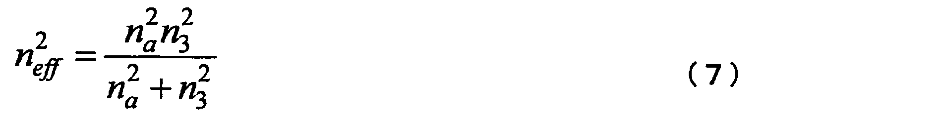
たとえば図4Bに示すような4層(有機EL層が3層、陰極導電層が1層)の場合の反射係数r1234は、上述した3層の場合の反射係数r123を用いて、再帰的に求めることができる。具体的には、次式(8)で、r234として前記r123を用いることで求めることができる。
図4Cに示すような5層の場合や6層以上の場合も同様に導くことが出来る。
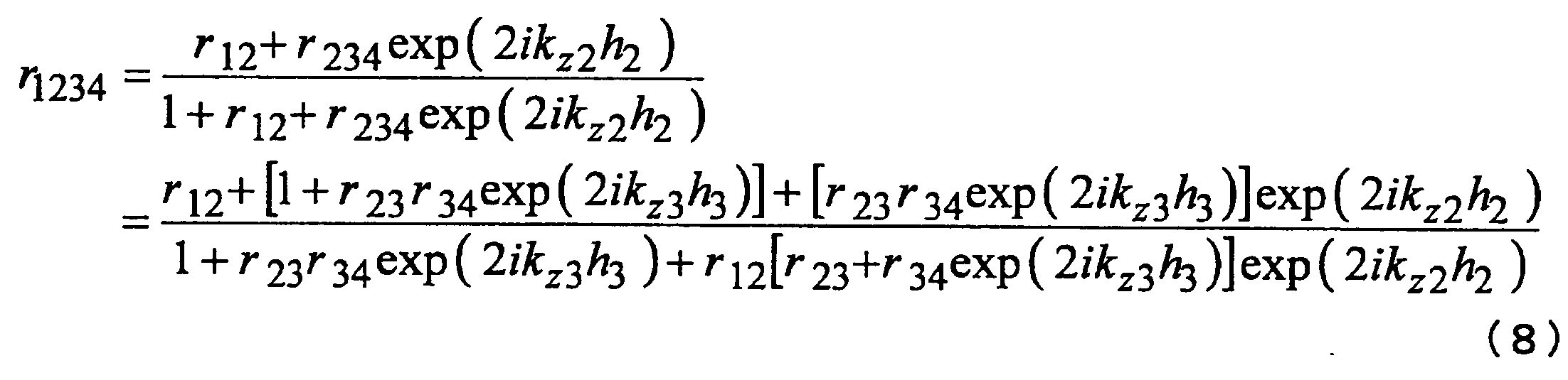
上述したように、前記凹部16の中心間の距離pは、凸部15の中心間の距離をレーザー回折法で測定することにより間接的に知ることが出来る。また同様に、凹部16の深さは、凸部15の高さをAFMにより測定することによって間接的に求めることが出来る。
以下、有機発光ダイオード10を構成する各層についてより詳細に説明する。
本実施形態において基板11には、可視光を透過する透明体が用いられる。
基板11を構成する材質としては、無機材料でも有機材料でもよく、それらの組み合わせでもよい。無機材料としては、たとえば、石英ガラス、無アルカリガラス、白板ガラス等の各種ガラス、マイカ等の透明無機鉱物などが挙げられる。有機材料としては、シクロオレフィン系フィルム、ポリエステル系フィルム等の樹脂フィルム、該樹脂フィルム中にセルロースナノファイバー等の微細繊維を混入した繊維強化プラスチック素材などが挙げられる。
用途にもよるが、一般に、基板11は可視光透過率の高いものを使用する。透過率は可視光の範囲(波長380nm~800nm)でスペクトルに偏りを与えず、透過率70%以上、好ましくは80%以上、より好ましくは90%以上のものを用いる。
本実施形態において陽極導電層12には、可視光を透過する透明導電体が用いられる。
陽極導電層12を構成する透明導電体は、特に限定されず、透明導電材料として公知のものが使用できる。たとえばインジウム-スズ酸化物(Indium Tin Oxide(ITO))、インジウム-亜鉛酸化物(Indium Zinc Oxide(IZO))、酸化亜鉛(Zinc Oxide(ZnO))、亜鉛-スズ酸化物(Zinc Tin Oxide(ZTO))等が挙げられる。
陽極導電層12の厚さは、通常、50~500nmである。
なお、有機発光ダイオード10を構成する各層の厚さは、分光エリプソメーター、接触式段差計、AFM等により測定できる。
本発明において有機EL(エレクトロルミネッセンス)層は、少なくとも、有機発光材料を含有する発光層を含む層であり、発光層のみから構成されてもよいが、一般的には発光層以外の他の層が含まれる。該他の層は、発光層の機能を損なわない限り、有機材料から構成されるものであっても無機材料から構成されるものであってもよい。
本実施形態において有機EL層13は、ホール注入層13a、ホール輸送層13b、発光層13c、電子輸送層13dおよび電子注入層13eの5層から構成される。これらの層の中で最も重要なものは発光層であり、たとえばホール注入層や電子注入層は層構成によっては省略できる。また、電子輸送層は発光層を兼ねることもできる。これらの層を構成する材質は、特に限定されず、公知のものが使用できる。
上記のうち、発光層13cを構成する材質としては、有機発光材料が用いられる。
有機発光材料としては、たとえば、Tris[1-phenylisoquinoline-C2,N]iridium(III)(Ir(piq)3)、1,4-bis[4-(N,N-diphenylaminostyrylbenzene)](DPAVB)、Bis[2-(2-benzoxazolyl)phenolato] Zinc(II)(ZnPBO)等の色素化合物が挙げられる。また、蛍光性色素化合物やりん光発光性材料を他の物質(ホスト材料)にドープしたものを用いてもよい。この場合、ホスト材料としては、ホール輸送材料、電子輸送材料等が挙げられる。
ホール注入層13a、ホール輸送層13b、電子輸送層13dを構成する材質としては、それぞれ、有機材料が一般的に用いられる。
たとえばホール注入層13aを構成する材質(ホール注入材料)としては、たとえば、4,4’,4”-tris(N,N-2-naphthylphenylamino)triphenylamine(2-TNATA)等の化合物などが挙げられる。
ホール輸送層13bを構成する材質(ホール輸送材料)としては、たとえば、N,N’-ジフェニル-N,N’-ビス(1-ナフチル)-(1,1’-ビフェニル)-4,4’-ジアミン(NPD)、銅フタロシアニン(CuPc)、N,N’-Diphenyl-N,N’-di(m-tolyl)benzidine(TPD)等の芳香族アミン化合物などが挙げられる。
電子輸送層13dを構成する材質(電子輸送材料)としては、たとえば、2,5-Bis(1-naphthyl)-1,3,4-oxadiazole(BND)、2-(4-tert-Butylphenyl)-5-(4-biphenylyl)-1,3,4-oxadiazole(PBD)等のオキサジオール系化合物、Tris(8-quinolinolato)aluminium(Alq)等の金属錯体系化合物などが挙げられる。
ただし陰極導電層14としてMg/Ag=10/90等のマグネシウム合金を使用すると、電子注入層13eを設けなくても、電子注入効果が得られる。
電子注入層13eを構成する材質としては、フッ化リチウム(LiF)などが使用できる。
有機EL層13全体の厚さは、通常、30~500nmである。
陰極導電層14はAgまたはAgの含有率が70質量%以上の合金からなる。
Agの含有率が70質量%以上の合金の具体例としては、たとえば上述したMg/Ag=10/90等のマグネシウム合金が挙げられる。
陰極導電層14の厚さは、通常、50~3000nmである。
有機発光ダイオード10の製造方法は特に限定されないが、好適には、基板11として、表面に、前記二次元格子構造に対応する、複数の凸部が二次元に周期的に配列した構造を有するものを作製し、前記構造上に、陽極導電層12と、有機EL層13(ホール注入層13a、ホール輸送層13b、発光層13c、電子輸送層13d、電子注入層13e)と、陰極導電層14とを順次積層することにより製造される。
そこで、本発明において、前記基板の作製方法としては、粒子単層膜をエッチングマスクとしたドライエッチング法が好ましい。この方法は、基材表面に、発光光の実効波長程度以下の一次粒子径を有する粒子の単層膜を、ラングミュアー・ブロジェット法(以下、LB法ともいう。)の原理を用いて作製することで、粒子間隔の制御が高精度で行われた2次元的最密充填格子が得られることを利用した方法であり、たとえば特開2009-158478号公報に詳細に開示されている。
該粒子単層膜においては、粒子が2次元に最密充填しているため、これをエッチングマスクとして基板原板表面をドライエッチングすることにより、高精度な三角格子(六方格子)状の二次元格子構造を形成できる。このような二次元格子構造を有する基板を用いて形成された陰極導電層14表面の二次元格子構造は高精度であることから、これを使用することによって、大面積である場合であっても高効率で表面プラズモンの回折波を得ることができ、光取出し効率がさらに向上し、高輝度の有機発光ダイオード10を得ることが可能となる。
以下、各工程についてより詳細に説明する。
被覆する工程は、水槽に、その液面上で粒子を展開させるための液体(下層液)を入れ、該下層液の液面に、溶剤中に粒子が分散した分散液を滴下し、溶剤を揮発させることにより粒子からなる粒子単層膜を液面上に形成する粒子単層膜形成工程と、粒子単層膜を基板上に移し取る移行工程とを行うことにより実施できる。
なお、ここでは粒子および有機溶剤としても疎水性のものを選択し、下層液として親水性のものを使用する例を示したが、粒子および有機溶剤として親水性のものを選択してもよく、下層液として、疎水性の液体を使用してもよい。
粒子単層膜形成工程では、まず、揮発性が高い溶剤(たとえばクロロホルム、メタノール、エタノール、メチルエチルケトン、メチルイソブチルケトン、ヘキサン等)中に、表面が疎水性の粒子を加えて分散液を調製する。別途、水槽(トラフ)を用意し、該水槽(トラフ)に、下層液として水(以下、下層水という場合もある。)を入れる。次に、前記分散液を前記下層水の液面に滴下すると、分散液中の粒子が分散媒によって下層水の液面上に展開する。そのため、分散媒である溶剤が揮発することで、粒子が2次元的に最密充填した単層膜が形成される。
また、該粒子は、粒子径の変動係数(標準偏差を平均値で除した値)が15%以下であることが好ましく、10%以下がより好ましく、5%以下がさらに好ましい。このように粒子径の変動係数が小さく、粒子径のばらつきが小さい粒子を使用すると、形成される粒子単層膜に、粒子が存在しない欠陥箇所が生じにくくなり、配列のずれが小さい粒子単層膜が形成できる。粒子単層膜の配列のずれが小さいと、最終的に陰極導電層14表面に形成される二次元格子構造における配列のずれも小さくなる。二次元格子構造における配列のずれが小さいほど陰極導電層14表面で表面プラズモンが効率的に光に変換されるため好ましい。
粒子単層膜を構成する粒子の材質としては、たとえば、Al、Au、Ti、Pt、Ag、Cu、Cr、Fe、Ni、Siなどの金属、SiO2、Al2O3、TiO2、MgO2、CaO2などの金属酸化物、ポリスチレン、ポリメチルメタクリレートなどの有機高分子、その他の半導体材料、無機高分子等が挙げられる。これらはいずれか1種を単独で用いても2種以上を併用してもよい。
この粒子の材質や後述するドライエッチング条件を選択することにより、形成される凸部の高さや形状、すなわち凹部16の深さや形状を調節できる。
上記で例示した粒子のうち、ポリスチレンなどの有機高分子の粒子は表面が疎水性であるため、そのまま使用できるが、金属粒子や金属酸化物粒子においては表面を疎水化剤により疎水性にすることにより使用できる。
疎水化剤としては、たとえば、界面活性剤、アルコキシシランなどが挙げられる。
界面活性剤としては、臭素化ヘキサデシルトリメチルアンモニウム、臭素化デシルトリメチルアンモニウムなどのカチオン性界面活性剤、ドデシル硫酸ナトリウム、4-オクチルベンゼンスルホン酸ナトリウムなどのアニオン性界面活性剤が好適に使用できる。また、アルカンチオール、ジスルフィド化合物、テトラデカン酸、オクタデカン酸なども使用できる。
このような界面活性剤を用いた疎水化処理は、有機溶剤や水などの液体に粒子を分散させて液中で行ってもよいし、乾燥状態にある粒子に対して行ってもよい。
液中で行う場合には、たとえば、クロロホルム、メタノール、エタノール、イソプロパノール、アセトン、メチルエチルケトン、エチルエチルケトン、トルエン、n-ヘキサン、シクロヘキサン、酢酸エチル、酢酸ブチルなどの1種以上からなる揮発性有機溶剤中に、疎水化対象の粒子を加えて分散させ、その後、界面活性剤を混合してさらに分散を続ければよい。このようにあらかじめ粒子を分散させておき、それから界面活性剤を加えると、表面をより均一に疎水化することができる。このような疎水化処理後の分散液は、そのまま、下層水の液面に滴下するための分散液として使用できる。
疎水化対象の粒子が水分散体の状態である場合には、この水分散体に界面活性剤を加えて水相で粒子表面の疎水化処理を行った後、有機溶剤を加えて疎水化処理済みの粒子を油相抽出する方法も有効である。こうして得られた分散液(有機溶剤中に粒子が分散した分散液)は、そのまま、下層水の液面に滴下するための分散液として使用できる。
なお、この分散液の粒子分散性を高めるためには、有機溶剤の種類と界面活性剤の種類とを適切に選択し、組み合わせることが好ましい。粒子分散性の高い分散液を使用することによって、粒子がクラスター状に凝集することを抑制でき、各粒子が高精度で2次元に最密充填した粒子単層膜がより得られやすくなる。たとえば、有機溶剤としてクロロホルムを選択する場合には、界面活性剤として臭素化デシルトリメチルアンモニウムを使用することが好ましい。その他にも、エタノールとドデシル硫酸ナトリウムとの組み合わせ、メタノールと4-オクチルベンゼンスルホン酸ナトリウムとの組み合わせ、メチルエチルケトンとオクダデカン酸との組み合わせなどを好ましく例示できる。
疎水化対象の粒子と界面活性剤の比率は、疎水化対象の粒子の質量に対して、界面活性剤の質量が1/3~1/15倍の範囲が好ましい。
また、こうした疎水化処理の際には、処理中の分散液を撹拌したり、分散液に超音波照射したりすることも粒子分散性向上の点で効果的である。
アルコキシシランとしては、モノメチルトリメトキシシラン、モノメチルトリエトキシシラン、ジメチルジエトキシシラン、フェニルトリエトキシシラン、ヘキシルトリメトキシシラン、デシルトリメトキシシラン、ビニルトリクロルシラン、ビニルトリメトキシシラン、ビニルトリエトキシシラン、2-(3,4エポキシシクロヘキシル)エチルトリメトキシシラン、3-グリシドキシプロピルトリメトキシシラン、3-グリシドキシプロピルメチルジエトキシシラン、3-グリシドキシプロピルトリエトキシシラン、p-スチリルトリメトキシシラン、3-メタクリロキシプロピルメチルジメトキシシラン、3-メタクリロキシプロピルトリメトキシシラン、3-メタクリロキシプロピルメチルジエトキシシラン、3-メタクリロキシプロピルトリエトキシシラン、3-アクリロキシプロピルトリメトキシシラン、N-2(アミノエチル)3-アミノプロピルメチルジメトキシシラン、N-2(アミノエチル)3-アミノプロピルトリメトキシシラン、N-2(アミノエチル)3-アミノプロピルトリエトキシシラン、3-アミノプロピルトリメトキシシラン、3-アミノプロピルトリエトキシシラン、N-フェニル-3-アミノプロピルトリメトキシシラン、3-ウレイドプロピルトリエトキシシラン、3-クロロプロピルトリメトキシシラン、3-メルカプトプロピルメチルジメトキシシラン、3-メルカプトプロピルトリメトキシシラン、3-イソシアネートプロピルトリエトキシシランなどが挙げられる。
疎水化剤としてアルコキシシランを用いる場合には、アルコキシシラン中のアルコキシシリル基がシラノール基に加水分解し、このシラノール基が粒子表面の水酸基に脱水縮合することで疎水化が行われる。よって、アルコキシシランを用いた疎水化は、水中で行うことが好ましい。
このように水中で疎水化を行う場合には、たとえば界面活性剤などの分散剤を併用して、疎水化前の粒子の分散状態を安定化するのが好ましい。ただし、分散剤の種類によってはアルコキシシランの疎水化効果が低減することもあるため、分散剤とアルコキシシランとの組み合わせは適切に選択する。
また、アミン系以外のアルコキシシランは、酸性またはアルカリ性の条件下で加水分解するため、反応時には分散液のpHを酸性またはアルカリ性に調整する必要がある。pHの調整法には制限はないが、0.1~2.0質量%濃度の酢酸水溶液を添加する方法によれば、加水分解促進の他に、シラノール基安定化の効果も得られるため好ましい。
疎水化対象の粒子とアルコキシシランの比率は、疎水化対象の粒子の質量に対して、アルコキシシランの質量が1/10~1/100倍の範囲が好ましい。
所定時間反応後、この分散液に対して、前述の揮発性有機溶剤のうちの1種以上を加え、水中で疎水化された粒子を油相抽出する。この際、添加する有機溶剤の体積は、有機溶剤添加前の分散液に対して0.3~3倍の範囲が好ましい。こうして得られた分散液(有機溶剤中に粒子が分散した分散液)は、そのまま、滴下工程において下層水の液面に滴下するための分散液として使用できる。なお、こうした疎水化処理においては、処理中の分散液の粒子分散性を高めるために、撹拌、超音波照射など実施することが好ましい。分散液の粒子分散性を高めることによって、粒子がクラスター状に凝集することを抑制でき、各粒子が高精度で2次元に最密充填した粒子単層膜がより得られやすくなる。
この際、超音波の出力は1~1200Wが好ましく、50~600Wがより好ましい。
また、超音波の周波数には特に制限はないが、たとえば28kHz~5MHzが好ましく、より好ましくは700kHz~2MHzである。一般的に振動数が高すぎると、水分子のエネルギー吸収が始まり、水面から水蒸気または水滴が立ち上る現象が起きるため、本発明のLB法にとって好ましくない。また、一般的に振動数が低すぎると、下層水中のキャビテーション半径が大きくなり、水中に泡が発生して水面に向かって浮上してくる。このような泡が粒子単層膜の下に集積すると、水面の平坦性が失われるため本発明の実施に不都合となる。また、超音波照射によって水面に定常波が発生する。いずれの周波数でも出力が高すぎたり、超音波振動子と発信機のチューニング条件によって水面の波高が高くなりすぎたりすると、粒子単層膜が水面波で破壊される可能性がある。
以上のことから超音波の周波数を適切に設定すると、形成されつつある粒子単層膜を破壊することなく、効果的に粒子の最密充填を促進することができる。しかし、粒子径がたとえば100nm以下など小さな粒子になると粒子の音響学的固有振動数は非常に高くなってしまうため、計算結果のとおりの超音波振動を与えるのは困難になる。
このような場合は、粒子2量体、3量体、・・・20量体程度までの質量に対応する固有振動を与えると仮定して計算を行うと、必要な振動数を現実的な範囲まで低減させることが出来る。粒子の会合体の固有振動数に対応する超音波振動を与えた場合でも、粒子の充填率向上効果は発現する。超音波の照射時間は、粒子の再配列が完了するのに十分であればよく、粒子径、超音波の周波数、水温などによって所要時間が変化する。しかし通常の作製条件では10秒間~60分間で行うのが好ましく、より好ましくは3分間~30分間である。
超音波照射によって得られる利点は粒子の最密充填化(ランダム配列を6方最密化する)の他に、分散液調製時に発生しやすい粒子の軟凝集体を破壊する効果、一度発生した点欠陥、線欠陥、または結晶転移などもある程度修復する効果がある。
特に、たとえばコロイダルシリカのように、球形であって粒子径の均一性も高い粒子が、水面上に浮いた状態で3つ集まり接触すると、粒子群の喫水線の合計長を最小にするように表面張力が作用し、3つの粒子は正三角形を基本とする配置で安定化する。仮に、喫水線が粒子群の頂点にくる場合、すなわち、粒子が液面下に潜ってしまう場合には、このような自己組織化は起こらず、粒子単層膜は形成されない。よって、粒子と下層水は、一方が疎水性である場合には他方を親水性にして、粒子群が液面下に潜ってしまわないようにすることが重要である。
下層液としては、以上の説明のように水を使用することが好ましく、水を使用すると、比較的大きな表面自由エネルギーが作用して、一旦生成した粒子の最密充填配置が液面上に安定的に持続しやすくなる。
移行工程では、粒子単層膜形成工程により下層水の液面上に形成された粒子単層膜を、単層状態のままエッチング対象物である基板原板上に移し取る。
粒子単層膜を基板原板上に移し取る具体的な方法には特に制限はなく、たとえば、疎水性の基板原板を粒子単層膜に対して略平行な状態に保ちつつ、上方から降下させて粒子単層膜に接触させ、ともに疎水性である粒子単層膜と基板との親和力により、粒子単層膜を基板原板に移行させ、移し取る方法;粒子単層膜を形成する前にあらかじめ水槽の下層水内に基板原板を略水平方向に配置しておき、粒子単層膜を液面上に形成した後に液面を徐々に降下させることにより、基板原板上に粒子単層膜を移し取る方法などがある。これらの方法によれば、特別な装置を使用せずに粒子単層膜を基板上に移し取ることができるが、より大面積の粒子単層膜であっても、その2次元的な最密充填状態を維持したまま基板原板上に移し取りやすい点で、いわゆるLBトラフ法を採用することが好ましい。
LBトラフ法では、水槽内の下層水中に基板原板をあらかじめ略鉛直方向に浸漬しておき、その状態で上述の粒子単層膜形成工程を行い、粒子単層膜を形成する。そして、粒子単層膜形成工程後に、基板原板を上方に引き上げることによって、粒子単層膜を基板原板上に移し取ることができる。
このとき、粒子単層膜は、粒子単層膜形成工程により液面上ですでに単層の状態に形成されているため、移行工程の温度条件(下層水の温度)や基板原板の引き上げ速度などが多少変動しても、粒子単層膜が崩壊して多層化するなどのおそれはない。
下層水の温度は、通常、季節や天気により変動する環境温度に依存し、ほぼ10~30℃程度である。
また、この際、水槽として、粒子単層膜の表面圧を計測するウィルヘルミープレート等を原理とする表面圧力センサーと、粒子単層膜を液面に沿う方向に圧縮する可動バリアとを具備するLBトラフ装置を使用すると、より大面積の粒子単層膜をより安定に基板原板上に移し取ることができる。このような装置によれば、粒子単層膜の表面圧を計測しながら、粒子単層膜を好ましい拡散圧(密度)に圧縮でき、また、基板原板の方に向けて一定の速度で移動させることができる。そのため、粒子単層膜の液面から基板原板上への移行が円滑に進行し、小面積の粒子単層膜しか基板原板上に移行できないなどのトラブルが生じにくい。
好ましい拡散圧は、5~80mNm-1であり、より好ましくは10~40mNm-1である。このような拡散圧であると、各粒子がより高精度で2次元に最密充填した粒子単層膜が得られやすい。また、基板原板を引き上げる速度は、0.5~20mm/分が好ましい。
移行工程の後、さらに、必要に応じて、粒子単層膜を基板原板上に固定するための固定工程を行ってもよい。粒子単層膜を基板原板上に固定することによって、この後のドライエッチング時に粒子が基板原板上を移動してしまう可能性が抑えられ、より安定かつ高精度に基板原板表面をエッチングすることができる。特に、ドライエッチングが進むにつれて、各粒子の直径が徐々に小さくなるため、基板原板上を移動する可能性が大きくなる。
固定工程の方法としては、バインダーを使用する方法や焼結法がある。
バインダーを使用する方法では、粒子単層膜が形成された基板原板の該粒子単層膜側にバインダー溶液を供給して粒子単層膜と基板原板との間にこれを浸透させる。
バインダーの使用量は、粒子単層膜の質量の0.001~0.02倍が好ましい。このような範囲であれば、バインダーが多すぎて粒子間にバインダーが詰まってしまい、粒子単層膜の精度に悪影響を与えるという問題を生じることなく、十分に粒子を固定することができる。バインダー溶液を多く供給してしまった場合には、バインダー溶液が浸透した後に、スピンコーターを使用したり、基板を傾けたりして、バインダー溶液の余剰分を除去すればよい。
バインダーの種類としては、先に疎水化剤として例示したアルコキシシランや一般の有機バインダー、無機バインダーなどを使用でき、バインダー溶液が浸透した後には、バインダーの種類に応じて、適宜加熱処理を行えばよい。アルコキシシランをバインダーとして使用する場合には、40~80℃で3~60分間の条件で加熱処理することが好ましい。
焼結法を採用する場合には、粒子単層膜が形成された基板原板を加熱して、粒子単層膜を構成している各粒子を基板に融着させればよい。加熱温度は粒子の材質と基板の材質に応じて決定すればよいが、粒子径が1μm以下の粒子はその物質本来の融点よりも低い温度で界面反応を開始するため、比較的低温側で焼結は完了する。加熱温度が高すぎると、粒子の融着面積が大きくなり、その結果、粒子単層膜としての形状が変化するなど、精度に影響を与える可能性がある。また、加熱を空気中で行うと基板や各粒子が酸化する可能性があるため、不活性ガス雰囲気下で行うことが好ましい。酸素を含む雰囲気下で焼結を行う場合は、後述のエッチング工程で酸化層を考慮した条件を設定することが必要となる。

Bの「粒子間のピッチ」とは、隣合う2つの粒子の頂点と頂点の距離であり、「平均ピッチ」とは、粒子単層膜内における平均値である。なお、粒子が球形であれば、隣合う粒子の頂点と頂点との距離は、隣合う粒子の中心と中心の距離と等しい。
粒子単層膜における粒子間の平均ピッチは、AFMにより、前記凸部15の中心間の距離pと同様にして求められる。
この粒子の配列のずれDが10%以下である粒子単層膜は、各粒子が2次元に最密充填し、粒子の間隔が制御されていて、その配列の精度が高い。
以上のようにして粒子単層膜で被覆された基板表面を、ドライエッチングすることにより、複数の凸部が周期的に二次元に配列した構造を有する基板を得ることができる。
具体的には、ドライエッチングを開始すると、まず、粒子単層膜を構成している各粒子の隙間をエッチングガスが通り抜けて基板原板の表面に到達し、その部分に凹部が形成され、各粒子に対応する位置にそれぞれ凸部が現れる。引き続きドライエッチングを続けると、各凸部上の粒子も徐々にエッチングされて小さくなり、同時に、基板原板表面の凹部も深くなっていく。そして、最終的には各粒子はドライエッチングにより消失し、それとともに基板原板の表面に、複数の凸部が周期的に二次元に配列した構造が形成される。
このとき、ドライエッチング条件(バイアス、ガス流量、堆積ガスの種類と量など)を調節することによって、形成される凸部の高さや形状を調節できる。
ドライエッチングに使用するエッチングガスとしては、たとえば、Ar、SF6、F2、CF4、C4F8、C5F8、C2F6、C3F6、C4F6、CHF3、CH2F2、CH3F、C3F8、Cl2、CCl4、SiCl4、BCl2、BCl3、BC2、Br2、Br3、HBr、CBrF3、HCl、CH4、NH3、O2、H2、N2、CO、CO2などが挙げられるが、本発明の効果を阻害しない範囲でこれらに限定されることは無い。粒子単層膜を構成する粒子や基板の材質などに応じて、これらのうちの1種以上を使用できる。
使用可能なエッチング装置としては、反応性イオンエッチング装置、イオンビームエッチング装置などの異方性エッチングが可能なものであって、最小で20W程度のバイアス電場を発生できるものであれば、プラズマ発生の方式、電極の構造、チャンバーの構造、高周波電源の周波数等の仕様に特に制限はない。
たとえば、粒子単層膜エッチングマスクを構成する粒子としてコロイダルシリカ粒子を選択し、基板として石英基板を選択してこれらを組み合わせた場合、エッチングガスにArやCF4などのガスを用いることで、比較的低い振幅とピッチの比のエッチングをすることができる。
また、電場のバイアスを数十から数百Wに設定すると、プラズマ状態にあるエッチングガス中の正電荷粒子は、加速されて高速でほぼ垂直に基板に入射する。よって、基板に対して反応性を有する気体を用いた場合は、垂直方向の物理化学エッチングの反応速度を高めることができる。
基板の材質とエッチングガスの種類の組み合わせによるが、ドライエッチングでは、プラズマによって生成したラジカルによる等方性エッチングも並行して起こる。ラジカルによるエッチングは化学エッチングであり、エッチング対象物のどの方向にも等方的にエッチングを行う。ラジカルは電荷を持たないためバイアスパワーの設定でエッチング速度をコントロールすることはできず、エッチングガスのチャンバー内濃度で操作することができる。荷電粒子による異方性エッチングを行うためにはある程度のガス圧を維持しなければならないので、反応性ガスを用いる限りラジカルの影響はゼロに出来ない。しかし、基材を冷却することでラジカルの反応速度を遅くする手法は広く用いられており、その機構を備えた装置も多いので、利用することが好ましい。
また、ドライエッチング工程において、主としてバイアスパワーを調整し、かつ状況に応じていわゆる堆積ガスを併用することで、基板表面に、凸部の中心間の距離と高さとの比(中心間の距離/高さ)が比較的低い二次元格子構造を形成することができる。
このメッシュ状金属層をドライエッチングのマスクとして使用すると、金属のない部分が削られていくので、凹型の孔を表面に多数有する微細構造体表面が得られる。
鋳型表面の構造の転写は、公知の方法、たとえば特開2009-158478号公報に開示されているような、ナノインプリント法、熱プレス法、射出成型法、UVエンボス法等の方法により実施できる。
転写回数が増えると微細凹凸の形状は鈍化するので、実用的な転写回数としては2または4回が好ましい。
これら各層の積層方法は、特に限定されず、一般的な有機発光ダイオードの製造において用いられている公知の方法を利用できる。たとえば、陽極導電層12および陰極導電層14は、それぞれ、スパッタリング法、真空蒸着法などによって形成できる。また、ホール注入層13a、ホール輸送層13b、発光層13c、電子輸送層13d、電子注入層13eは、真空蒸着法によって形成される。
これら各層の厚さは非常に薄いため、上記のように各層を順次積層することで、基板11表面の構造が陰極導電層14まで反映され、有機EL層13側の表面に前記二次元周期構造を有する陰極導電層14が形成される。
たとえば、本実施形態では、有機EL層13が、ホール注入層13a、ホール輸送層13b、発光層13c、電子輸送層13d、電子注入層13eの5層から構成される例を示したが、本発明はこれに限定されない。たとえば、ホール注入層13a、ホール輸送層13b、発光層13c、電子輸送層13d、電子注入層13eのうちの二つ以上の層の機能を一つの層が兼ね備えてもよい。また、発光層13cは必須であるが、その他の層、たとえばホール注入層13aやホール輸送層13b、電子輸送層13d、電子注入層13eは省略してもよい。最も単純な系は、有機EL層13が発光層13cのみから構成されるものである。
また、電子注入層13eを設けた例を示したが、陰極導電層14が電子注入層の機能を兼ね備える場合は、電子注入層13eを設けなくてもよい。たとえば陰極導電層14をMg/Ag=10/90等のマグネシウム合金で構成すると、上述したように、電子注入効果が得られ、陰極導電層14が電子注入層の機能を兼ね備えたものとなる。
本発明の第二の態様の有機発光ダイオードは、基板上に、少なくとも、AgまたはAgの含有率が70質量%以上の合金からなる陰極導電層と、発光層を含む有機EL層と、陽極導電層とが順次積層され、前記陰極導電層の前記有機EL層側の表面に、複数の凹部が周期的に二次元に配列した二次元格子構造が設けられた有機発光ダイオードにおいて、
有機発光ダイオードからの光の取出し波長λ(nm)と、前記二次元格子構造における前記凹部の中心間の距離p(nm)とが、それらの関係を示すグラフにて下記座標A、B、C、D、E、F、G、H、I、J、Aを順次結ぶ直線で囲まれた領域内にあり、かつ前記凹部の深さが15nm以上70nm以下であることを特徴とする有機発光ダイオードである。
A(λ=450、p=258+W(1/2))、B(λ=500、p=319+W(1/2))、C(λ=600、p=406+W(1/2))、D(λ=700、p=484+W(1/2))、E(λ=800、p=561+W(1/2))、F(λ=800、p=493-W(1/2))、G(λ=700、p=425-W(1/2))、H(λ=600、p=353-W(1/2))、I(λ=500、p=262-W(1/2))、J(λ=450、p=110-W(1/2))[ここで、W(1/2)は、前記発光層を構成する発光材料のスペクトルにおける発光ピークの半値半幅を示す。]
以下、本態様の有機発光ダイオードを、添付の図面を参照して説明する。なお、以下に記載する実施形態において、前出の図面に示した構成に対応する構成には、同一の符号を付してその詳細な説明を省略する。
図5は、本態様の有機発光ダイオードの一実施形態の構成の一部の概略断面図である。
本実施形態の有機発光ダイオード20は、基板21上に、陰極導電層14と、有機EL層13と、陽極導電層12と、が順次積層されている。
有機EL層13は、陰極導電層14側から順次積層された電子注入層13e、電子輸送層13d、発光層13c、ホール輸送層13bおよびホール注入層13aから構成される。
陽極導電層12および陰極導電層14には電圧が印加できるようになっている。
基板21を構成する材質としては前記基板11と同様のものが挙げられる。ただし本態様においては、光が基板21とは反対側から取り出されるため、基板21は必ずしも透明でなくてもよい。
陰極導電層14、有機EL層13、陽極導電層12はそれぞれ前記と同様である。
基板21の作製方法としては、たとえば、フォトリソグラフィー、電子ビームリソグラフィー、機械式切削加工、レーザー加工、二光束干渉露光、縮小露光などが挙げられる。
しかし、上述したように、これらのうちの二光束干渉露光以外の手法は、大面積に周期格子構造を作製するのに適さないため、工業的な利用面において面積の制約を受ける。また、二光束干渉露光は、ある程度の小面積は作製可能であるが、一辺が数cm以上の大面積の場合は光学セットアップ全体に対する振動、風、熱収縮・膨張、空気の揺らぎ、電圧変動、等々の様々な外乱因子が影響して、均一で正確な周期格子構造を作製することはきわめて困難である。
したがって、本態様においても、基板21の作製に、前記基板11と同様、粒子単層膜をエッチングマスクとしたドライエッチング法を利用することが好ましい。
粒子単層膜をエッチングマスクとしたドライエッチング法を利用した基板21の作製は、たとえば、表面に、前記二次元格子構造に対応する、複数の凸部が周期的に二次元に配列した構造を有する鋳型を、粒子単層膜をエッチングマスクとしたドライエッチング法によって作製し、該鋳型表面の構造を基板原板に奇数回転写することにより実施できる。
粒子単層膜をエッチングマスクとしたドライエッチング法による鋳型の作製は、前記第一の態様における基板の作製と同様の手順で実施できる。
鋳型表面の構造の転写は、公知の方法、たとえば特開2009-158478号公報に開示されているような、ナノインプリント法、熱プレス法、射出成型法、UVエンボス法等の方法により実施できる。
転写回数が増えると微細凹凸の形状は鈍化するので、実用的な転写回数としては1または3回が好ましい。
また、他の方法として、粒子単層膜を利用して作製する金属メッシュマスクを利用する方法がある。すなわち、基板原板の表面に粒子単層膜を作製した後、粒子単層膜の上からCr、Ni、Fe、Coなどの金属を真空蒸着し、しかる後に粒子単層膜をふき取る操作を行う。真空蒸着の際に粒子マスクの隙間から金属が基板原板の表面に到達するが、一方で粒子の真下に金属は蒸着されない。したがって、真空蒸着後に粒子をふき取ると、粒子が存在していた箇所に孔が開いたメッシュ状の金属蒸着層からなるマスクが形成される。
このメッシュ状金属層をドライエッチングのマスクとして使用すると、金属のない部分が削られていくので、凹型の孔を表面に多数有する微細構造体表面が得られる。
本発明の第三の態様の有機発光ダイオードは、基板上に、少なくとも、陽極導電層と、有機発光材料を含有する発光層を含む有機エレクトロルミネッセンス層と、AgまたはAgの含有率が70質量%以上の合金からなる陰極導電層とが順次積層され、前記陰極導電層の前記有機エレクトロルミネッセンス層側の表面に、複数の凸部が周期的に二次元に配列した二次元格子構造が設けられた有機発光ダイオードにおいて、
有機発光ダイオードからの光の取出し波長λ(nm)と、前記二次元格子構造における前記凸部の中心間の距離p(nm)とが、それらの関係を示すグラフにて下記座標A、B、C、D、E、F、G、H、I、J、Aを順次結ぶ直線で囲まれた領域内にあり、かつ前記凸部の高さが12nm以上180nm以下であることを特徴とする有機発光ダイオード。
A(λ=450、p=258+W(1/2))、B(λ=500、p=319+W(1/2))、C(λ=600、p=406+W(1/2))、D(λ=700、p=484+W(1/2))、E(λ=800、p=561+W(1/2))、F(λ=800、p=493-W(1/2))、G(λ=700、p=425-W(1/2))、H(λ=600、p=353-W(1/2))、I(λ=500、p=262-W(1/2))、J(λ=450、p=110-W(1/2))[ここで、W(1/2)は、前記発光層を構成する発光材料のスペクトルにおける発光ピークの半値半幅を示す。]
以下、本態様の有機発光ダイオードを、添付の図面を参照して説明する。なお、以下に記載する実施形態において、前出の図面に示した構成に対応する構成には、同一の符号を付してその詳細な説明を省略する。
図8は、本態様の有機発光ダイオードの一実施形態の構成の一部の概略断面図である。
本実施形態の有機発光ダイオード110は、基板111上に、陽極導電層12と、有機EL層13と、陰極導電層14と、が順次積層されている。
有機EL層13は、陽極導電層12側から順次積層されたホール注入層13a、ホール輸送層13b、発光層13c、電子輸送層13dおよび電子注入層13eから構成される。
陽極導電層12および陰極導電層14には電圧が印加できるようになっている。
基板111を構成する材質としては前記基板11と同様のものが挙げられる。
陰極導電層14、有機EL層13、陽極導電層12はそれぞれ前記と同様である。
基板111は、前記第二の態様の基板21と同様に製造することができ、好ましい製造方法も、前記基板21の好ましい製造方法と同様である。
本発明の第四の態様の有機発光ダイオードは、基板上に、少なくとも、AgまたはAgの含有率が70質量%以上の合金からなる陰極導電層と、有機発光材料を含有する発光層を含む有機エレクトロルミネッセンス層と、陽極導電層とが順次積層され、前記陰極導電層の前記有機エレクトロルミネッセンス層側の表面に、複数の凸部が周期的に二次元に配列した二次元格子構造が設けられた有機発光ダイオードにおいて、
有機発光ダイオードからの光の取出し波長λ(nm)と、前記二次元格子構造における前記凸部の中心間の距離p(nm)とが、それらの関係を示すグラフにて下記座標A、B、C、D、E、F、G、H、I、J、Aを順次結ぶ直線で囲まれた領域内にあり、かつ前記凸部の高さが12nm以上180nm以下であることを特徴とする有機発光ダイオード。
A(λ=450、p=258+W(1/2))、B(λ=500、p=319+W(1/2))、C(λ=600、p=406+W(1/2))、D(λ=700、p=484+W(1/2))、E(λ=800、p=561+W(1/2))、F(λ=800、p=493-W(1/2))、G(λ=700、p=425-W(1/2))、H(λ=600、p=353-W(1/2))、I(λ=500、p=262-W(1/2))、J(λ=450、p=110-W(1/2))[ここで、W(1/2)は、前記発光層を構成する発光材料のスペクトルにおける発光ピークの半値半幅を示す。]
以下、本態様の有機発光ダイオードを、添付の図面を参照して説明する。なお、以下に記載する実施形態において、前出の図面に示した構成に対応する構成には、同一の符号を付してその詳細な説明を省略する。
図9は、本態様の有機発光ダイオードの一実施形態の構成の一部の概略断面図である。
本実施形態の有機発光ダイオード120は、基板121上に、陰極導電層14と、有機EL層13と、陽極導電層12と、が順次積層されている。
有機EL層13は、陰極導電層14側から順次積層された電子注入層13e、電子輸送層13d、発光層13c、ホール輸送層13bおよびホール注入層13aから構成される。
陽極導電層12および陰極導電層14には電圧が印加できるようになっている。
基板121を構成する材質としては前記基板21と同様のものが挙げられる。
陰極導電層14、有機EL層13、陽極導電層12はそれぞれ前記と同様である。
基板121は、前記第一の態様の基板11と同様に製造することができ、好ましい製造方法も、前記基板11の好ましい製造方法と同様である。
本発明の第五の態様の有機発光ダイオードは、基板上に、少なくとも、陽極導電層と、有機発光材料を含有する発光層を含む有機エレクトロルミネッセンス層と、AlまたはAlの含有率が70質量%以上の合金からなる陰極導電層とが順次積層され、前記陰極導電層の前記有機エレクトロルミネッセンス層側の表面に、複数の凹部が周期的に二次元に配列した二次元格子構造が設けられた有機発光ダイオードにおいて、
有機発光ダイオードからの光の取出し波長λ(nm)と、前記二次元格子構造における前記凹部の中心間の距離p(nm)とが、それらの関係を示すグラフにて下記座標A´、B´、C´、D´、E´、F´、G´、H´、I´、J´、K´、L´、A´を順次結ぶ直線で囲まれた領域内にあり、かつ前記凹部の深さが12nm以上180nm以下であることを特徴とする有機発光ダイオード。
A´(λ=300、p=220+W(1/2))、B´(λ=400、p=295+W(1/2))、C´(λ=500、p=368+W(1/2))、D´(λ=600、p=438+W(1/2))、E´(λ=700、p=508+W(1/2))、F´(λ=800、p=575+W(1/2))、G´(λ=800、p=505-W(1/2))、H´(λ=700、p=438-W(1/2))、I´(λ=600、p=368-W(1/2))、J´(λ=500、p=298-W(1/2))、K´(λ=400、p=225-W(1/2))、L´(λ=300、p=150-W(1/2))[ここで、W(1/2)は、前記発光層を構成する発光材料のスペクトルにおける発光ピークの半値半幅を示す。]
以下、本態様の有機発光ダイオードを、添付の図面を参照して説明する。なお、以下に記載する実施形態において、前出の図面に示した構成に対応する構成には、同一の符号を付してその詳細な説明を省略する。
図1は、本態様の有機発光ダイオードの一実施形態の構成の一部の概略断面図をも表す。
本実施形態の有機発光ダイオード210は、基板11上に、陽極導電層12と、有機EL層13と、AlまたはAlの含有率が70質量%以上の合金からなる陰極導電層214と、が順次積層されている。
有機EL層13は、陽極導電層12側から順次積層されたホール注入層13a、ホール輸送層13b、発光層13c、電子輸送層13dおよび電子注入層13eから構成される。
陽極導電層12および陰極導電層214には電圧が印加できるようになっている。
陰極導電層214は、AlまたはAlの含有率が70質量%以上の合金からなる。
陰極導電層214の厚さは、通常、50~3000nmである。
基板11、陽極導電層12、有機EL層13はそれぞれ前記と同様である。
本発明は表面プラズモンへ変換されるエネルギーの割合が大きい有機発光ダイオードに対して特に有効である。陰極金属層の発光層側表面から発光層までの距離としては、たとえば、100nm以下、より近い距離として、たとえば、50nm以下の有機発光ダイオードに対して有効である。
A´(λ=300、p=220+W(1/2))、B´(λ=400、p=295+W(1/2))、C´(λ=500、p=368+W(1/2))、D´(λ=600、p=438+W(1/2))、E´(λ=700、p=508+W(1/2))、F´(λ=800、p=575+W(1/2))、G´(λ=800、p=505-W(1/2))、H´(λ=700、p=438-W(1/2))、I´(λ=600、p=368-W(1/2))、J´(λ=500、p=298-W(1/2))、K´(λ=400、p=225-W(1/2))、L´(λ=300、p=150-W(1/2))
W(1/2)は、前記第一の態様におけるW(1/2)と同様の意味を有する。
取出し波長λ(nm)は、表面プラズモンから輻射光としてエネルギーを取り出したときの波長であり、最も普通には発光材料の発光ピーク波長となる。
この特定の取出し波長がλ1[λ1は300nm~800nmの範囲内の特定の値である。]であるとき、凹部16の中心間の距離pは、前記領域内のλ=λ1の座標に対応する任意の値をとり得る。たとえばλ1が600nmである場合、距離pは、[368-W(1/2)]nmから[438+W(1/2)]nmまでの任意の値をとり得る。
図10は、取出し波長λ(nm)を横軸に、凹部の中心間の距離p(nm)を縦軸にとったグラフである。
図10に示すとおり、座標A´、B´、C´、D´、E´、F´はそれぞれ座標(λ、p)=(300、220)、(400、295)、(500、368)、(600、438)、(700、508)、(800、575)のpをプラス方向にW(1/2)シフトさせた座標であり、座標G´、H´、I´、J´、K´、L´はそれぞれ座標(λ、p)=(800、505)、(700、438)、(600、368)、(500、298)、(400、225)、(300、150)の距離pをマイナス方向にW(1/2)シフトさせた座標である。このシフト幅がW(1/2)を超えると、光の取出し効率は向上するものの、その効果は、シフト幅がW(1/2)以内である場合に比べて大きく劣る。
前記シフト幅は、少ないほどよく、1/5Wが好ましく、1/10Wがより好ましく、0が特に好ましい。すなわち、取出し波長λ(nm)と、凹部16の中心間の距離p(nm)とは、それらの関係を示すグラフにて座標(λ、p)=(300、220)、(400、295)、(500、368)、(600、438)、(700、508)、(800、575)、(800、505)、(700、438)、(600、368)、(500、298)、(400、225)、(300、150)を順次結ぶ直線で囲まれた領域内にあることが特に好ましい。
以下に、前記座標を特定するための、表面プラズモンから光への変換効率の計算方法は、前記第一の態様において説明した計算方法を適用することができ、図3に示すモデルにおける陰極導電層14は銀をアルミニウムに換えて計算することができる。
ここで、反射率は、有機EL層の屈折率nを1.6、1.7または1.8と仮定して、単色平面波の波長(取出し波長λに対応)が300nm、400nm、500nm、600nm、700nm、800nmである場合について、穴の中心間の間隔pと深さdを系統的に変えて計算した。
本態様の基板11は、前記第一の態様の基板11と同様に製造することができ、好ましい製造方法も、前記第一の態様の基板11の好ましい製造方法と同様である。
本発明の第二の態様の有機発光ダイオードは、基板上に、少なくとも、AlまたはAlの含有率が70質量%以上の合金からなる陰極導電層と、有機発光材料を含有する発光層を含む有機エレクトロルミネッセンス層と、陽極導電層とが順次積層され、前記陰極導電層の前記有機エレクトロルミネッセンス層側の表面に、複数の凹部が周期的に二次元に配列した二次元格子構造が設けられた有機発光ダイオードにおいて、
有機発光ダイオードからの光の取出し波長λ(nm)と、前記二次元格子構造における前記凹部の中心間の距離p(nm)とが、それらの関係を示すグラフにて下記座標A´、B´、C´、D´、E´、F´、G´、H´、I´、J´、K´、L´、A´を順次結ぶ直線で囲まれた領域内にあり、かつ前記凹部の深さが12nm以上180nm以下であることを特徴とする有機発光ダイオード。
A´(λ=300、p=220+W(1/2))、B´(λ=400、p=295+W(1/2))、C´(λ=500、p=368+W(1/2))、D´(λ=600、p=438+W(1/2))、E´(λ=700、p=508+W(1/2))、F´(λ=800、p=575+W(1/2))、G´(λ=800、p=505-W(1/2))、H´(λ=700、p=438-W(1/2))、I´(λ=600、p=368-W(1/2))、J´(λ=500、p=298-W(1/2))、K´(λ=400、p=225-W(1/2))、L´(λ=300、p=150-W(1/2))[ここで、W(1/2)は、前記発光層を構成する発光材料のスペクトルにおける発光ピークの半値半幅を示す。]
以下、本態様の有機発光ダイオードを、添付の図面を参照して説明する。なお、以下に記載する実施形態において、前出の図面に示した構成に対応する構成には、同一の符号を付してその詳細な説明を省略する。
図5は、本態様の有機発光ダイオードの一実施形態の構成の一部の概略断面図をも表す。
本実施形態の有機発光ダイオード220は、基板21上に、陰極導電層214と、有機EL層13と、陽極導電層12と、が順次積層されている。
有機EL層13は、陰極導電層214側から順次積層された電子注入層13e、電子輸送層13d、発光層13c、ホール輸送層13bおよびホール注入層13aから構成される。
陽極導電層12および陰極導電層214には電圧が印加できるようになっている。
基板21、陰極導電層214、有機EL層13、陽極導電層12はそれぞれ前記と同様である。
本発明の第七の態様の有機発光ダイオードは、基板上に、少なくとも、陽極導電層と、有機発光材料を含有する発光層を含む有機エレクトロルミネッセンス層と、AlまたはAlの含有率が70質量%以上の合金からなる陰極導電層とが順次積層され、前記陰極導電層の前記有機エレクトロルミネッセンス層側の表面に、複数の凸部が周期的に二次元に配列した二次元格子構造が設けられた有機発光ダイオードにおいて、
有機発光ダイオードからの光の取出し波長λ(nm)と、前記二次元格子構造における前記凸部の中心間の距離p(nm)とが、それらの関係を示すグラフにて下記座標A´、B´、C´、D´、E´、F´、G´、H´、I´、J´、K´、L´、A´を順次結ぶ直線で囲まれた領域内にあり、かつ前記凸部の高さが12nm以上180nm以下であることを特徴とする有機発光ダイオード。
A´(λ=300、p=220+W(1/2))、B´(λ=400、p=295+W(1/2))、C´(λ=500、p=368+W(1/2))、D´(λ=600、p=438+W(1/2))、E´(λ=700、p=508+W(1/2))、F´(λ=800、p=575+W(1/2))、G´(λ=800、p=505-W(1/2))、H´(λ=700、p=438-W(1/2))、I´(λ=600、p=368-W(1/2))、J´(λ=500、p=298-W(1/2))、K´(λ=400、p=225-W(1/2))、L´(λ=300、p=150-W(1/2))[ここで、W(1/2)は、前記発光層を構成する発光材料のスペクトルにおける発光ピークの半値半幅を示す。]
以下、本態様の有機発光ダイオードを、添付の図面を参照して説明する。なお、以下に記載する実施形態において、前出の図面に示した構成に対応する構成には、同一の符号を付してその詳細な説明を省略する。
図8は、本態様の有機発光ダイオードの一実施形態の構成の一部の概略断面図をも表す。
本実施形態の有機発光ダイオード310は、基板111上に、陽極導電層12と、有機EL層13と、陰極導電層214と、が順次積層されている。
有機EL層13は、陽極導電層12側から順次積層されたホール注入層13a、ホール輸送層13b、発光層13c、電子輸送層13dおよび電子注入層13eから構成される。
陽極導電層12および陰極導電層214には電圧が印加できるようになっている。
基板111、陰極導電層214、有機EL層13、陽極導電層12はそれぞれ前記と同様である。
基板111は、前記第二の態様の基板21と同様に製造することができ、好ましい製造方法も、前記基板21の好ましい製造方法と同様である。
本発明の第八の態様の有機発光ダイオードは、基板上に、少なくとも、AlまたはAlの含有率が70質量%以上の合金からなる陰極導電層と、有機発光材料を含有する発光層を含む有機エレクトロルミネッセンス層と、陽極導電層とが順次積層され、前記陰極導電層の前記有機エレクトロルミネッセンス層側の表面に、複数の凸部が周期的に二次元に配列した二次元格子構造が設けられた有機発光ダイオードにおいて、
有機発光ダイオードからの光の取出し波長λ(nm)と、前記二次元格子構造における前記凸部の中心間の距離p(nm)とが、それらの関係を示すグラフにて下記座標A´、B´、C´、D´、E´、F´、G´、H´、I´、J´、K´、L´、A´を順次結ぶ直線で囲まれた領域内にあり、かつ前記凸部の高さが12nm以上180nm以下であることを特徴とする有機発光ダイオード。
A´(λ=300、p=220+W(1/2))、B´(λ=400、p=295+W(1/2))、C´(λ=500、p=368+W(1/2))、D´(λ=600、p=438+W(1/2))、E´(λ=700、p=508+W(1/2))、F´(λ=800、p=575+W(1/2))、G´(λ=800、p=505-W(1/2))、H´(λ=700、p=438-W(1/2))、I´(λ=600、p=368-W(1/2))、J´(λ=500、p=298-W(1/2))、K´(λ=400、p=225-W(1/2))、L´(λ=300、p=150-W(1/2))[ここで、W(1/2)は、前記発光層を構成する発光材料のスペクトルにおける発光ピークの半値半幅を示す。]
以下、本態様の有機発光ダイオードを、添付の図面を参照して説明する。なお、以下に記載する実施形態において、前出の図面に示した構成に対応する構成には、同一の符号を付してその詳細な説明を省略する。
図9は、本態様の有機発光ダイオードの一実施形態の構成の一部の概略断面図をも表す。
本実施形態の有機発光ダイオード320は、基板121上に、陰極導電層214と、有機EL層13と、陽極導電層12と、が順次積層されている。
有機EL層13は、陰極導電層214側から順次積層された電子注入層13e、電子輸送層13d、発光層13c、ホール輸送層13bおよびホール注入層13aから構成される。
陽極導電層12および陰極導電層214には電圧が印加できるようになっている。
基板121、陰極導電層214、有機EL層13、陽極導電層12はそれぞれ前記と同様である。
基板121は、前記第一の態様の基板11と同様に製造することができ、好ましい製造方法も、前記基板11の好ましい製造方法と同様である。
なお、前記二次元格子構造が正方格子である場合、前期凹部の中心間の距離p(nm)、または前記凸部の中心間の距離p(nm)の座標の値に、それぞれ(√3/2)を乗じて補正することが好ましい。そして、そのような態様の有機発光ダイオードにおいても、光取出し効率が飛躍的に向上し、高強度の発光が得られる。
したがって、本発明の有機発光ダイオードは、画像表示装置、照明装置等に有用である。低電圧駆動が可能になることから、有機EL素子の寿命を飛躍的に延ばすことが可能になり、また省エネルギーである。さらに、光取出し効率が高いことから、明るい画像表示装置や照明装置が得られる。
[実施例1]
平均粒子径が395.0nmで、粒子径の変動係数が4.0%である球形コロイダルシリカの5.0質量%水分散体(分散液)を用意した。なお、平均粒子径および粒子径の変動係数は、Malvern Instruments Ltd製 Zetasizer Nano-ZSによる粒子動的光散乱法で求めた粒度分布をガウス曲線にフィッティングさせて得られるピークから求めた。
ついで、この分散液を孔径1.2μmφのメンブランフィルターでろ過し、メンブランフィルターを通過した分散液に濃度1.0質量%のフェニルトリエトキシシランの加水分解物水溶液を加え、約40℃で3時間反応させた。この際、フェニルトリエトキシシランの質量がコロイダルシリカ粒子の質量の0.015倍となるように分散液と加水分解水溶液とを混合した。
ついで、反応終了後の分散液に、この分散液の体積の5倍の体積のメチルイソブチルケトンを加えて十分に攪拌して、疎水化されたコロイダルシリカを油相抽出した。
こうして得られた濃度1.05質量%の疎水化コロイダルシリカ分散液を、粒子単層膜の表面圧を計測する表面圧力センサーと、粒子単層膜を液面に沿う方向に圧縮する可動バリアとを備えた水槽(LBトラフ装置)中の液面(下層水として水を使用、水温26.5℃)に滴下速度0.01mL/秒で滴下した。なお、水槽の下層水には、あらかじめ有機発光ダイオードの透明基板として用いるための石英基板(30mm×30mm×1.0mm、両面鏡面研磨)を略鉛直方向に浸漬しておいた。
その後、超音波(出力100W、周波数1500kHz)を下層水中から水面に向けて10分間照射して粒子が2次元的に最密充填するのを促しつつ、分散液の溶剤であるメチルイソブチルケトンを揮発させ、粒子単層膜を形成させた。
ついで、この粒子単層膜を、可動バリアにより、拡散圧が22~30mNm-1になるまで圧縮し、石英基板を3mm/分の速度で引き上げ、基板の片面上に水面の粒子単層膜を移し取った。
ついで、粒子単層膜が形成された石英基板上にバインダーとして0.15質量%モノメチルトリメトキシシランの加水分解液を浸透させ、その後、加水分解液の余剰分をスピンコーター(3000rpm)で1分間処理して除去した。その後、これを100℃で10分間加熱してバインダーを反応させ、コロイダルシリカからなる粒子単層膜付き石英基板を得た。
ドライエッチング後、得られた基板表面を原子間力顕微鏡(AFM)による観察したところ、断面形状が図6に示すような円錐台形である凸部が三角格子状に配置された微細構造が形成されていた。
このようにして基板表面に形成された微細構造における凸部の中心間の距離p’(格子定数)をレーザー回折法により測定したところ、3回の試験の平均値で395.0nmであった。また、該微細構造における凸部の平均高さhを、AFM像から無作為に選択された合計25カ所の5μm×5μmの領域における平均値を求め、それら25カ所それぞれの平均値をさらに平均することにより求めたところ、30.9nmであった。また、配列のずれD’は4.9%であった。また、上記で求めた値から算出される、平均高さhと中心間の距離p’の平均値との比(中心間の距離p’/平均高さh)は0.078であった。
ドライエッチング条件を変更したことを除いて、実施例1と全く同じ操作で作製したボトムエミッション型有機発光ダイオードを得た。
このとき石英基板表面に形成された微細構造の凸部の中心間の距離は395.0nmであり、凸部の平均高さは100nmであった。
石英基板表面に微細構造を形成しなかった以外は、実施例1と全く同じ操作でボトムエミッション型有機発光ダイオードを得た。したがって、この素子の基板の表面は平坦である。
球形コロイダルシリカの平均粒子径を変更したことを除いて、実施例1と全く同じ操作で作製したボトムエミッション型有機発光ダイオードを得た。
このとき石英基板表面に形成された微細構造の凸部の中心間の距離は306.9nmであり、凸部の平均高さは30.9nmであった。また、配列のずれD’は11.01%であった。
ドライエッチング条件を変更したことを除いて、実施例1と全く同じ操作で作製したボトムエミッション型有機発光ダイオードを得た。
このとき石英基板表面に形成された微細構造の凸部の中心間の距離は395.0nmであり、凸部の平均高さは10.2nmであった。また、配列のずれD’は4.9%であった。
ドライエッチング条件を変更したことを除いて、実施例1と全く同じ操作で作製したボトムエミッション型有機発光ダイオードを得た。
このとき石英基板表面に形成された微細構造の凸部の中心間の距離は395.0nmであり、凸部の平均高さは192.0nmであった。
[1.取出し波長λ(nm)と、陰極導電層表面の二次元格子構造における凹部の中心間の距離p(nm)との関係を示すグラフの作製]
実施例1、2、比較例1~4で得たボトムエミッション型有機発光ダイオードについて、発光層を構成する発光材料(Ir(piq)3をPH1に5%濃度でドープしたもの)の発光スペクトルにおけるピークの半値半幅W(1/2)を、ピーク上の作図により求めたところ、40nmであった。W(1/2)が40nmである場合の座標A~Jを図7に示す。
また、実施例1、2、比較例1~4で得たボトムエミッション型有機発光ダイオードの構成における取出し波長を発光スペクトルの波形分離により求めたところ、625nmであった。
したがって、取出し波長625nmに対応する、上記座標A~Jで囲まれる領域内となる凹部の中心間の距離pの範囲は335nm~467nmである。
実施例1、2、比較例1~4で得たボトムエミッション型有機発光ダイオードにおいては、石英基板表面に形成した微細構造における凸部の中心間の間隔および平均高さは、その上に積層された陰極導電層の電子輸送層側の表面に形成された二次元周期構造における凹部の中心間の間隔および平均深さと一致する。
したがって、凹部の中心間の間隔が、335nm~467nmの範囲内の395.0nmであり且つ凹部の深さが30.9nmである実施例1のボトムエミッション型有機発光ダイオードは本発明の範囲内である。また、凹部の中心間の間隔が、実施例1と同様に395.0nmであり且つ凹部の深さが100nmである実施例2のボトムエミッション型有機発光ダイオードは本発明の範囲内である。一方、比較例2のボトムエミッション型有機発光ダイオードは、凹部の中心間の間隔が306.9nmである点で本発明の範囲外であり、比較例3のボトムエミッション型有機発光ダイオードは、凹部の深さが10.2nmである点で本発明の範囲外であり、比較例4のボトムエミッション型有機発光ダイオードは、凹部の深さが192.0nmである点で本発明の範囲外である。
実施例1、2、比較例1~4で得たボトムエミッション型有機発光ダイオードそれぞれについて、下記手順で発光効率特性および輝度特性を評価した。
得られたボトムエミッション型有機発光ダイオードを30mA/cm2の電流密度で発光させたときの垂直方向の輝度(cd/m2)を輝度計にて測定し、電流密度あたりの輝度特性(電流密度(mA/cm2)-輝度(cd/m2))を求めた。また、輝度を測定する際に電圧も測定しておき、輝度から光束(lm)を換算し、電流密度あたりの発光効率(電流密度(mA/cm2)-発光効率(lm/W))を求めた。
それらの測定結果から、電流密度あたりの発光効率、輝度それぞれについて、実施例1の測定値の、比較例1の測定値に対する向上率を下記式により算出した。実施例2、比較例2~4についても同様に、比較例1の測定値に対する向上率を算出した。その結果を表1に示す。
向上率=(実施例1の測定値-比較例1の測定値)/比較例1の測定値×100
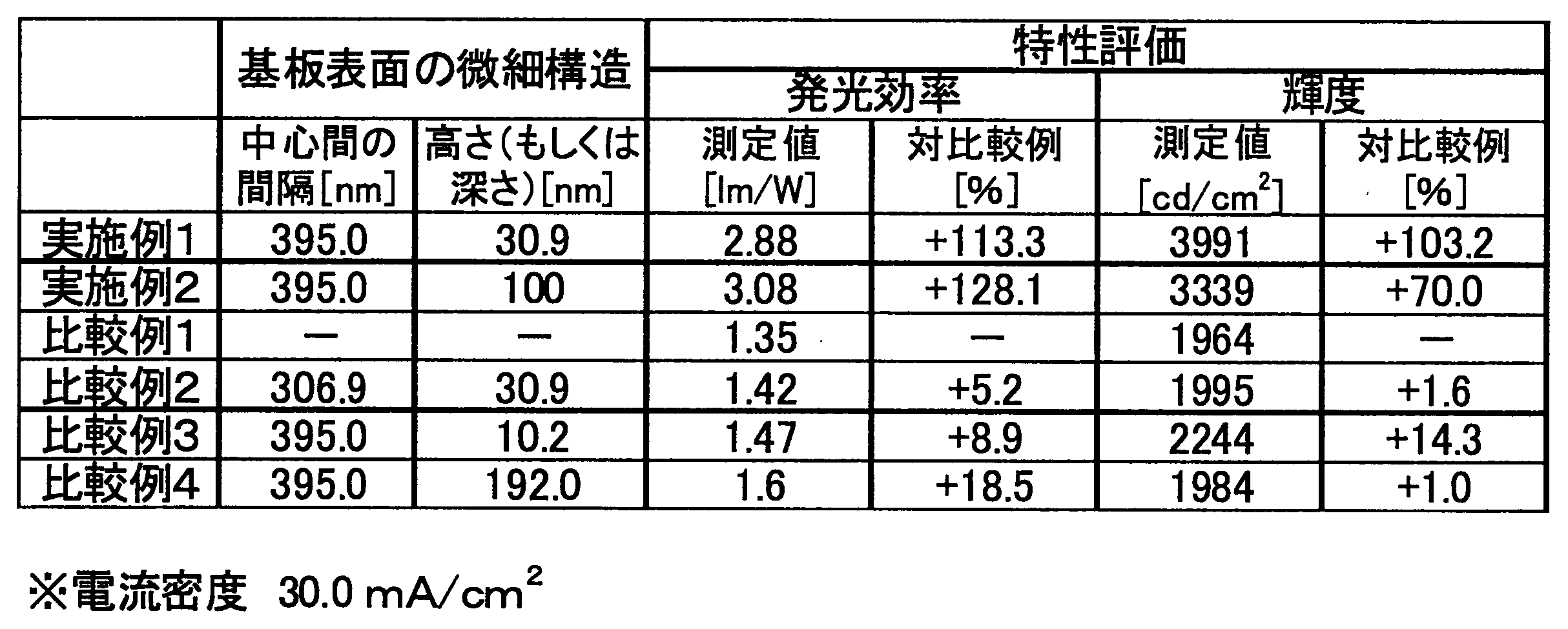
球形コロイダルシリカの平均粒子径およびドライエッチング条件を変更して基板を作製し、発光材料として、Rubreneをホスト材料(Alq3)に1%濃度でドープしたものを用いた以外は、実施例1と全く同じ操作でボトムエミッション型有機発光ダイオードを得た。
このとき石英基板表面に形成された微細構造の凸部の中心間の距離は350.0nmであり、凸部の平均高さは70nmであった。
石英基板表面に微細構造を形成しなかった以外は、実施例3と全く同じ操作でボトムエミッション型有機発光ダイオードを得た。したがって、この素子の基板の表面は平坦である。
球形コロイダルシリカの平均粒子径を変更したことを除いて、実施例3と全く同じ操作で作製したボトムエミッション型有機発光ダイオードを得た。
このとき石英基板表面に形成された微細構造の凸部の中心間の距離は500.0nmであり、凸部の平均高さは70nmであった。
[1.取出し波長λ(nm)と、陰極導電層表面の二次元格子構造における凹部の中心間の距離p(nm)との関係を示すグラフの作製]
実施例3、比較例5および6で得たボトムエミッション型有機発光ダイオードについて、発光層を構成する発光材料(Rubreneをホスト材料(Alq3)に1%濃度でドープしたも)の発光スペクトルにおけるピークの半値半幅W(1/2)を、ピーク上の作図により求めたところ、40nmであった。W(1/2)が40nmである場合の座標A~Jを図7に示す。
また、実施例3、比較例5および6で得たボトムエミッション型有機発光ダイオードの構成における取出し波長を発光スペクトルの波形分離により求めたところ、565nmであった。
したがって、取出し波長565nmに対応する、上記座標A~Jで囲まれる領域内となる凹部の中心間の距離pの範囲は280nm~416nmである。
実施例3、比較例5および6で得たボトムエミッション型有機発光ダイオードにおいては、石英基板表面に形成した微細構造における凸部の中心間の間隔および平均高さは、その上に積層された陰極導電層の電子輸送層側の表面に形成された二次元周期構造における凹部の中心間の間隔および平均深さと一致する。
したがって、凹部の中心間の間隔が、280nm~416nmの範囲内の350.0nmであり且つ凹部の深さが70nmである実施例3のボトムエミッション型有機発光ダイオードは本発明の範囲内である。一方、比較例6のボトムエミッション型有機発光ダイオードは、凹部の中心間の間隔が500.0nmである点で本発明の範囲外である。
実施例3、比較例5および6で得たボトムエミッション型有機発光ダイオードそれぞれについて、試験例1と同様に発光効率特性および輝度特性を評価した。
また、実施例3の測定値の、比較例5の測定値に対する向上率を試験例1と同様に算出した。比較例6についても同様に、比較例5の測定値に対する向上率を算出した。その結果を表2に示す。

球形コロイダルシリカの平均粒子径およびドライエッチング条件を変更して基板を作製し、発光材料として、FIlpicをKLHS-04に8%濃度でドープしたものを用い、陰極導電層をAlで成膜した以外は、実施例1と全く同じ操作でボトムエミッション型有機発光ダイオードを得た。
このとき石英基板表面に形成された微細構造の凸部の中心間の距離は300.0nmであり、凸部の平均高さは31.2nmであった。
石英基板表面に微細構造を形成しなかった以外は、実施例4と全く同じ操作でボトムエミッション型有機発光ダイオードを得た。したがって、この素子の基板の表面は平坦である。
[比較例8]
球形コロイダルシリカの平均粒子径およびドライエッチング条件を変更したことを除いて、実施例4と全く同じ操作で作製したボトムエミッション型有機発光ダイオードを得た。
このとき石英基板表面に形成された微細構造の凸部の中心間の距離は395.0nmであり、凸部の平均高さは30.2nmであった。
<試験例3>
[1.取出し波長λ(nm)と、陰極導電層表面の二次元格子構造における凹部または凸部の中心間の距離p(nm)との関係を示すグラフの作製]
実施例4、比較例7および8で得たボトムエミッション型有機発光ダイオードについて、発光層を構成する発光材料(FIlipicをKLHS-04に8%濃度でドープしたもの)の発光スペクトルにおけるピークの半値半幅W(1/2)を、ピーク上の作図により求めたところ、20nmであった。W(1/2)が20nmである場合の座標A´~L´を図11に示す。
したがって、取出し波長470nmに対応する、上記座標A´~L´で囲まれる領域内となる凹部の中心間の距離pの範囲は256nm~366nmである。
実施例4、比較例7および8で得たボトムエミッション型有機発光ダイオードにおいては、石英基板表面に形成した微細構造における凸部の中心間の間隔および平均高さは、その上に積層された陰極導電層の電子輸送層側の表面に形成された二次元周期構造における凹部の中心間の間隔および平均深さと一致する。
したがって、凹部の中心間の距離が、256nm~366nmの範囲内の300.0nmであり且つ凹部の深さが31.2nmである実施例4のボトムエミッション型有機発光ダイオードは本発明の範囲内である。一方、比較例8のボトムエミッション型有機発光ダイオードは、凹部の中心間の距離が395.0nmである点で本発明の範囲外である。
[2.発光効率特性および輝度特性の評価]
実施例4、比較例7および8で得たボトムエミッション型有機発光ダイオードそれぞれについて、試験例1と同様に発光効率特性および輝度特性を評価した。
また、実施例4の測定値の、比較例7の測定値に対する向上率を試験例1と同様に算出した。比較例8についても同様に、比較例7の測定値に対する向上率を算出した。その結果を表3に示す。
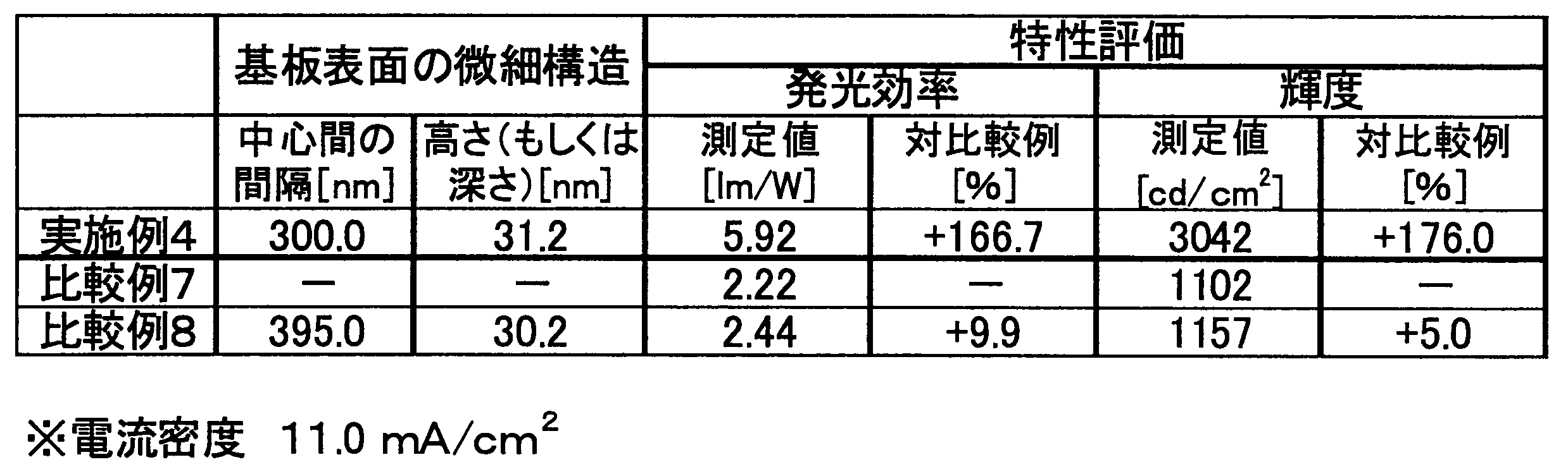
Claims (23)
- 基板上に、少なくとも、陽極導電層と、有機発光材料を含有する発光層を含む有機エレクトロルミネッセンス層と、AgまたはAgの含有率が70質量%以上の合金からなる陰極導電層とが順次積層され、前記陰極導電層の前記有機エレクトロルミネッセンス層側の表面に、複数の凹部が周期的に二次元に配列した二次元格子構造が設けられた有機発光ダイオードにおいて、
有機発光ダイオードからの光の取出し波長λ(nm)と、前記二次元格子構造における前記凹部の中心間の距離p(nm)とが、それらの関係を示すグラフにて下記座標A、B、C、D、E、F、G、H、I、J、Aを順次結ぶ直線で囲まれた領域内にあり、かつ前記凹部の深さが12nm以上180nm以下であることを特徴とする有機発光ダイオード。
A(λ=450、p=258+W(1/2))、B(λ=500、p=319+W(1/2))、C(λ=600、p=406+W(1/2))、D(λ=700、p=484+W(1/2))、E(λ=800、p=561+W(1/2))、F(λ=800、p=493-W(1/2))、G(λ=700、p=425-W(1/2))、H(λ=600、p=353-W(1/2))、I(λ=500、p=262-W(1/2))、J(λ=450、p=110-W(1/2))[ここで、W(1/2)は、前記発光層を構成する発光材料のスペクトルにおける発光ピークの半値半幅を示す。] - 請求項1に記載の有機発光ダイオードを製造する方法であって、
表面に、前記二次元格子構造に対応する、複数の凸部が周期的に二次元に配列した構造を有する基板を作製し、前記構造上に、前記陽極導電層と、前記有機エレクトロルミネッセンス層と、前記陰極導電層とを順次積層することを特徴とする有機発光ダイオードの製造方法。 - 前記基板が、粒子単層膜をエッチングマスクとしたドライエッチング法によって作製される、請求項2に記載の有機発光ダイオードの製造方法。
- 前記二次元格子構造を鋳型にして前記基板を作製することを含み、
前記鋳型が、粒子単層膜をエッチングマスクとしたドライエッチング法によって作製された原盤であるか、または前記原盤を転写して得られる金属電鋳型もしくは樹脂型である、請求項2に記載の有機発光ダイオードの製造方法。 - 基板上に、少なくとも、AgまたはAgの含有率が70質量%以上の合金からなる陰極導電層と、有機発光材料を含有する発光層を含む有機エレクトロルミネッセンス層と、陽極導電層とが順次積層され、前記陰極導電層の前記有機エレクトロルミネッセンス層側の表面に、複数の凹部が周期的に二次元に配列した二次元格子構造が設けられた有機発光ダイオードにおいて、
有機発光ダイオードからの光の取出し波長λ(nm)と、前記二次元格子構造における前記凹部の中心間の距離p(nm)とが、それらの関係を示すグラフにて下記座標A、B、C、D、E、F、G、H、I、J、Aを順次結ぶ直線で囲まれた領域内にあり、かつ前記凹部の深さが12nm以上180nm以下であることを特徴とする有機発光ダイオード。
A(λ=450、p=258+W(1/2))、B(λ=500、p=319+W(1/2))、C(λ=600、p=406+W(1/2))、D(λ=700、p=484+W(1/2))、E(λ=800、p=561+W(1/2))、F(λ=800、p=493-W(1/2))、G(λ=700、p=425-W(1/2))、H(λ=600、p=353-W(1/2))、I(λ=500、p=262-W(1/2))、J(λ=450、p=110-W(1/2))[ここで、W(1/2)は、前記発光層を構成する発光材料のスペクトルにおける発光ピークの半値半幅を示す。] - 請求項5に記載の有機発光ダイオードを製造する方法であって、
表面に、前記二次元格子構造に対応する、複数の凹部が周期的に二次元に配列した構造を有する基板を作製し、前記構造上に、前記陰極導電層と、前記有機エレクトロルミネッセンス層と、前記陽極導電層とを順次積層することを特徴とする有機発光ダイオードの製造方法。 - 前記二次元格子構造を鋳型にして前記基板を作製することを含み、
前記鋳型が、粒子単層膜をエッチングマスクとしたドライエッチング法によって作製された原盤であるか、または前記原盤を転写して得られる金属電鋳型もしくは樹脂型である、請求項6に記載の有機発光ダイオードの製造方法。 - 前記基板が、表面に粒子単層膜を作製した後、前記粒子単層膜の上から、Cr、Ni、FeおよびCoからなる群より選択される金属を真空蒸着して前記粒子単層膜の粒子の隙間から前記基板の原板の表面に到達したメッシュ状の金属蒸着層を作製した後、前記粒子単層膜を除去し、前記メッシュ状の金属蒸着層をエッチングマスクとしたドライエッチング法によって作製される、請求項6に記載の有機発光ダイオードの製造方法。
- 基板上に、少なくとも、陽極導電層と、有機発光材料を含有する発光層を含む有機エレクトロルミネッセンス層と、AgまたはAgの含有率が70質量%以上の合金からなる陰極導電層とが順次積層され、前記陰極導電層の前記有機エレクトロルミネッセンス層側の表面に、複数の凸部が周期的に二次元に配列した二次元格子構造が設けられた有機発光ダイオードにおいて、
有機発光ダイオードからの光の取出し波長λ(nm)と、前記二次元格子構造における前記凸部の中心間の距離p(nm)とが、それらの関係を示すグラフにて下記座標A、B、C、D、E、F、G、H、I、J、Aを順次結ぶ直線で囲まれた領域内にあり、かつ前記凸部の高さが12nm以上180nm以下であることを特徴とする有機発光ダイオード。
A(λ=450、p=258+W(1/2))、B(λ=500、p=319+W(1/2))、C(λ=600、p=406+W(1/2))、D(λ=700、p=484+W(1/2))、E(λ=800、p=561+W(1/2))、F(λ=800、p=493-W(1/2))、G(λ=700、p=425-W(1/2))、H(λ=600、p=353-W(1/2))、I(λ=500、p=262-W(1/2))、J(λ=450、p=110-W(1/2))[ここで、W(1/2)は、前記発光層を構成する発光材料のスペクトルにおける発光ピークの半値半幅を示す。] - 基板上に、少なくとも、AgまたはAgの含有率が70質量%以上の合金からなる陰極導電層と、有機発光材料を含有する発光層を含む有機エレクトロルミネッセンス層と、陽極導電層とが順次積層され、前記陰極導電層の前記有機エレクトロルミネッセンス層側の表面に、複数の凸部が周期的に二次元に配列した二次元格子構造が設けられた有機発光ダイオードにおいて、
有機発光ダイオードからの光の取出し波長λ(nm)と、前記二次元格子構造における前記凸部の中心間の距離p(nm)とが、それらの関係を示すグラフにて下記座標A、B、C、D、E、F、G、H、I、J、Aを順次結ぶ直線で囲まれた領域内にあり、かつ前記凸部の高さが12nm以上180nm以下であることを特徴とする有機発光ダイオード。
A(λ=450、p=258+W(1/2))、B(λ=500、p=319+W(1/2))、C(λ=600、p=406+W(1/2))、D(λ=700、p=484+W(1/2))、E(λ=800、p=561+W(1/2))、F(λ=800、p=493-W(1/2))、G(λ=700、p=425-W(1/2))、H(λ=600、p=353-W(1/2))、I(λ=500、p=262-W(1/2))、J(λ=450、p=110-W(1/2))[ここで、W(1/2)は、前記発光層を構成する発光材料のスペクトルにおける発光ピークの半値半幅を示す。] - 基板上に、少なくとも、陽極導電層と、有機発光材料を含有する発光層を含む有機エレクトロルミネッセンス層と、AlまたはAlの含有率が70質量%以上の合金からなる陰極導電層とが順次積層され、前記陰極導電層の前記有機エレクトロルミネッセンス層側の表面に、複数の凹部が周期的に二次元に配列した二次元格子構造が設けられた有機発光ダイオードにおいて、
有機発光ダイオードからの光の取出し波長λ(nm)と、前記二次元格子構造における前記凹部の中心間の距離p(nm)とが、それらの関係を示すグラフにて下記座標A´、B´、C´、D´、E´、F´、G´、H´、I´、J´、K´、L´、A´を順次結ぶ直線で囲まれた領域内にあり、かつ前記凹部の深さが12nm以上180nm以下であることを特徴とする有機発光ダイオード。
A´(λ=300、p=220+W(1/2))、B´(λ=400、p=295+W(1/2))、C´(λ=500、p=368+W(1/2))、D´(λ=600、p=438+W(1/2))、E´(λ=700、p=508+W(1/2))、F´(λ=800、p=575+W(1/2))、G´(λ=800、p=505-W(1/2))、H´(λ=700、p=438-W(1/2))、I´(λ=600、p=368-W(1/2))、J´(λ=500、p=298-W(1/2))、K´(λ=400、p=225-W(1/2))、L´(λ=300、p=150-W(1/2))[ここで、W(1/2)は、前記発光層を構成する発光材料のスペクトルにおける発光ピークの半値半幅を示す。] - 基板上に、少なくとも、AlまたはAlの含有率が70質量%以上の合金からなる陰極導電層と、有機発光材料を含有する発光層を含む有機エレクトロルミネッセンス層と、陽極導電層とが順次積層され、前記陰極導電層の前記有機エレクトロルミネッセンス層側の表面に、複数の凹部が周期的に二次元に配列した二次元格子構造が設けられた有機発光ダイオードにおいて、
有機発光ダイオードからの光の取出し波長λ(nm)と、前記二次元格子構造における前記凹部の中心間の距離p(nm)とが、それらの関係を示すグラフにて下記座標A´、B´、C´、D´、E´、F´、G´、H´、I´、J´、K´、L´、A´を順次結ぶ直線で囲まれた領域内にあり、かつ前記凹部の深さが12nm以上180nm以下であることを特徴とする有機発光ダイオード。
A´(λ=300、p=220+W(1/2))、B´(λ=400、p=295+W(1/2))、C´(λ=500、p=368+W(1/2))、D´(λ=600、p=438+W(1/2))、E´(λ=700、p=508+W(1/2))、F´(λ=800、p=575+W(1/2))、G´(λ=800、p=505-W(1/2))、H´(λ=700、p=438-W(1/2))、I´(λ=600、p=368-W(1/2))、J´(λ=500、p=298-W(1/2))、K´(λ=400、p=225-W(1/2))、L´(λ=300、p=150-W(1/2))[ここで、W(1/2)は、前記発光層を構成する発光材料のスペクトルにおける発光ピークの半値半幅を示す。] - 基板上に、少なくとも、陽極導電層と、有機発光材料を含有する発光層を含む有機エレクトロルミネッセンス層と、AlまたはAlの含有率が70質量%以上の合金からなる陰極導電層とが順次積層され、前記陰極導電層の前記有機エレクトロルミネッセンス層側の表面に、複数の凸部が周期的に二次元に配列した二次元格子構造が設けられた有機発光ダイオードにおいて、
有機発光ダイオードからの光の取出し波長λ(nm)と、前記二次元格子構造における前記凸部の中心間の距離p(nm)とが、それらの関係を示すグラフにて下記座標A´、B´、C´、D´、E´、F´、G´、H´、I´、J´、K´、L´、A´を順次結ぶ直線で囲まれた領域内にあり、かつ前記凸部の高さが12nm以上180nm以下であることを特徴とする有機発光ダイオード。
A´(λ=300、p=220+W(1/2))、B´(λ=400、p=295+W(1/2))、C´(λ=500、p=368+W(1/2))、D´(λ=600、p=438+W(1/2))、E´(λ=700、p=508+W(1/2))、F´(λ=800、p=575+W(1/2))、G´(λ=800、p=505-W(1/2))、H´(λ=700、p=438-W(1/2))、I´(λ=600、p=368-W(1/2))、J´(λ=500、p=298-W(1/2))、K´(λ=400、p=225-W(1/2))、L´(λ=300、p=150-W(1/2))[ここで、W(1/2)は、前記発光層を構成する発光材料のスペクトルにおける発光ピークの半値半幅を示す。] - 基板上に、少なくとも、AlまたはAlの含有率が70質量%以上の合金からなる陰極導電層と、有機発光材料を含有する発光層を含む有機エレクトロルミネッセンス層と、陽極導電層とが順次積層され、前記陰極導電層の前記有機エレクトロルミネッセンス層側の表面に、複数の凸部が周期的に二次元に配列した二次元格子構造が設けられた有機発光ダイオードにおいて、
有機発光ダイオードからの光の取出し波長λ(nm)と、前記二次元格子構造における前記凸部の中心間の距離p(nm)とが、それらの関係を示すグラフにて下記座標A´、B´、C´、D´、E´、F´、G´、H´、I´、J´、K´、L´、A´を順次結ぶ直線で囲まれた領域内にあり、かつ前記凸部の高さが12nm以上180nm以下であることを特徴とする有機発光ダイオード。
A´(λ=300、p=220+W(1/2))、B´(λ=400、p=295+W(1/2))、C´(λ=500、p=368+W(1/2))、D´(λ=600、p=438+W(1/2))、E´(λ=700、p=508+W(1/2))、F´(λ=800、p=575+W(1/2))、G´(λ=800、p=505-W(1/2))、H´(λ=700、p=438-W(1/2))、I´(λ=600、p=368-W(1/2))、J´(λ=500、p=298-W(1/2))、K´(λ=400、p=225-W(1/2))、L´(λ=300、p=150-W(1/2))[ここで、W(1/2)は、前記発光層を構成する発光材料のスペクトルにおける発光ピークの半値半幅を示す。] - 前記凹部の深さが15nm以上70nm以下であることを特徴とする請求項1、5、11または12に記載の有機発光ダイオード。
- 前記凹部の形状が前記基板上の円錐台形状または円柱形状を転写した形状であって、かつ深さが15nm以上70nm以下であることを特徴とする請求項1、5、11または12に記載の有機発光ダイオード。
- 前記凹部の形状が前記基板上の正弦波形状を転写した形状であって、かつ深さが50nm以上160nm以下であることを特徴とする請求項1、5、11または12に記載の有機発光ダイオード。
- 前記凹部の形状が前記基板上の円錐形状を転写した形状であって、かつ深さが60nm以上170nm以下であることを特徴とする請求項1、5、11または12に記載の有機発光ダイオード。
- 前記凸部の形状が前記基板上の円錐台形状または円柱形状であって、かつ高さが15nm以上70nm以下であることを特徴とする請求項9、10、13または14に記載の有機発光ダイオード。
- 前記凸部の形状が前記基板上の正弦波形状であって、かつ高さが50nm以上160nm以下であることを特徴とする請求項9、10、13または14に記載の有機発光ダイオード。
- 前記凸部の形状が前記基板上の円錐形状であって、かつ高さが60nm以上170nm以下であることを特徴とする請求項9、10、13または14に記載の有機発光ダイオード。
- 請求項1、5、および9ないし14のいずれか一項に記載の有機発光ダイオードを備える画像表示装置。
- 請求項1、5、および9ないし14のいずれか一項に記載の有機発光ダイオードを備える照明装置。
Priority Applications (9)
| Application Number | Priority Date | Filing Date | Title |
|---|---|---|---|
| CN201180063944.8A CN103460797B (zh) | 2010-11-02 | 2011-11-02 | 有机发光二极管及其制造方法、图像显示装置及照明装置 |
| KR1020137013506A KR101430971B1 (ko) | 2010-11-02 | 2011-11-02 | 유기 발광 다이오드 및 그 제조 방법, 화상 표시 장치 및 조명 장치 |
| JP2012541894A JP5283206B2 (ja) | 2010-11-02 | 2011-11-02 | 有機発光ダイオードおよびその製造方法、画像表示装置および照明装置 |
| EP11838054.2A EP2637480B1 (en) | 2010-11-02 | 2011-11-02 | Organic light emitting diode, image display device, and illuminating device |
| US13/882,848 US9246122B2 (en) | 2010-11-02 | 2011-11-02 | Organic light emitting diode, method for manufacturing same, image display device, and illuminating device |
| US14/965,619 US9728751B2 (en) | 2010-11-02 | 2015-12-10 | Organic light emitting diode, method for manufacturing same, image display device, and illuminating device |
| US15/636,477 US10050233B2 (en) | 2010-11-02 | 2017-06-28 | Organic light emitting diode, method for manufacturing same, image display device, and illuminating device |
| US16/034,211 US10566574B2 (en) | 2010-11-02 | 2018-07-12 | Organic light emitting diode, method for manufacturing same, image display device, and illuminating device |
| US16/743,473 US20200168841A1 (en) | 2010-11-02 | 2020-01-15 | Organic light emitting diode, image display device and illuminating device |
Applications Claiming Priority (2)
| Application Number | Priority Date | Filing Date | Title |
|---|---|---|---|
| JP2010-246653 | 2010-11-02 | ||
| JP2010246653 | 2010-11-02 |
Related Child Applications (2)
| Application Number | Title | Priority Date | Filing Date |
|---|---|---|---|
| US13/882,848 A-371-Of-International US9246122B2 (en) | 2010-11-02 | 2011-11-02 | Organic light emitting diode, method for manufacturing same, image display device, and illuminating device |
| US14/965,619 Division US9728751B2 (en) | 2010-11-02 | 2015-12-10 | Organic light emitting diode, method for manufacturing same, image display device, and illuminating device |
Publications (1)
| Publication Number | Publication Date |
|---|---|
| WO2012060404A1 true WO2012060404A1 (ja) | 2012-05-10 |
Family
ID=46024517
Family Applications (1)
| Application Number | Title | Priority Date | Filing Date |
|---|---|---|---|
| PCT/JP2011/075285 Ceased WO2012060404A1 (ja) | 2010-11-02 | 2011-11-02 | 有機発光ダイオードおよびその製造方法、画像表示装置および照明装置 |
Country Status (7)
| Country | Link |
|---|---|
| US (5) | US9246122B2 (ja) |
| EP (1) | EP2637480B1 (ja) |
| JP (3) | JP5283206B2 (ja) |
| KR (1) | KR101430971B1 (ja) |
| CN (1) | CN103460797B (ja) |
| TW (2) | TWI596750B (ja) |
| WO (1) | WO2012060404A1 (ja) |
Cited By (10)
| Publication number | Priority date | Publication date | Assignee | Title |
|---|---|---|---|---|
| WO2013099915A1 (ja) | 2011-12-28 | 2013-07-04 | 王子ホールディングス株式会社 | 有機発光ダイオード、有機発光ダイオードの製造方法、画像表示装置および照明装置 |
| WO2013179339A1 (ja) * | 2012-05-30 | 2013-12-05 | 株式会社 日立製作所 | 有機発光素子、光源装置およびそれらの製造方法 |
| WO2014069565A1 (ja) * | 2012-10-31 | 2014-05-08 | 昭和電工株式会社 | 有機el素子並びにそれを備えた画像表示装置及び照明装置 |
| WO2014084220A1 (ja) * | 2012-11-27 | 2014-06-05 | 昭和電工株式会社 | 有機el素子並びにそれを備えた画像表示装置及び照明装置 |
| JP2014130769A (ja) * | 2012-12-28 | 2014-07-10 | Oji Holdings Corp | 有機発光ダイオード、有機発光ダイオード用基板およびその製造方法 |
| JP2015028927A (ja) * | 2013-06-27 | 2015-02-12 | 王子ホールディングス株式会社 | 有機発光ダイオード、有機発光ダイオード用基板の製造方法、画像表示装置および照明装置 |
| WO2017099086A1 (ja) * | 2015-12-10 | 2017-06-15 | 王子ホールディングス株式会社 | 基板、光学素子、金型、有機発光素子、有機薄膜太陽電池、および、基板の製造方法 |
| US9865836B2 (en) | 2013-11-11 | 2018-01-09 | Konica Minolta Laboratory U.S.A., Inc. | Broadband light emitting device with grating-structured electrode |
| WO2023100672A1 (ja) * | 2021-12-03 | 2023-06-08 | ソニーセミコンダクタソリューションズ株式会社 | 表示装置および電子機器 |
| JP2023540880A (ja) * | 2020-08-20 | 2023-09-27 | アプライド マテリアルズ インコーポレイテッド | Oled光照射野アーキテクチャ |
Families Citing this family (41)
| Publication number | Priority date | Publication date | Assignee | Title |
|---|---|---|---|---|
| US9246122B2 (en) | 2010-11-02 | 2016-01-26 | Oji Holdings Corporation | Organic light emitting diode, method for manufacturing same, image display device, and illuminating device |
| WO2013005638A1 (ja) * | 2011-07-01 | 2013-01-10 | 王子製紙株式会社 | 有機発光ダイオードの製造方法、有機発光ダイオード、画像表示装置、照明装置および基板 |
| US9991463B2 (en) * | 2012-06-14 | 2018-06-05 | Universal Display Corporation | Electronic devices with improved shelf lives |
| JP6101784B2 (ja) * | 2013-03-06 | 2017-03-22 | Jxエネルギー株式会社 | 凹凸構造を有する部材の製造方法及びそれにより製造された凹凸構造を有する部材 |
| US9494792B2 (en) * | 2013-07-30 | 2016-11-15 | Global Oled Technology Llc | Local seal for encapsulation of electro-optical element on a flexible substrate |
| CN103715359A (zh) * | 2013-10-21 | 2014-04-09 | 昆山维信诺显示技术有限公司 | 一种oled器件及其制作方法 |
| DE102013111785B4 (de) * | 2013-10-25 | 2025-12-24 | Pictiva Displays International Limited | Verfahren zum Herstellen eines optoelektronischen Bauelementes |
| WO2015097877A1 (ja) * | 2013-12-27 | 2015-07-02 | パイオニアOledライティングデバイス株式会社 | 光装置及び光装置の製造方法 |
| JP2015141841A (ja) * | 2014-01-29 | 2015-08-03 | パイオニア株式会社 | 発光装置 |
| US10211428B2 (en) * | 2014-06-24 | 2019-02-19 | President And Fellows Of Harvard College | Metal-based optical device enabling efficient light generation from emitters on a high-index absorbing substrate |
| CN104103673B (zh) * | 2014-07-09 | 2017-06-20 | 京东方科技集团股份有限公司 | 一种oled显示器及其制备方法 |
| US9761842B2 (en) * | 2014-12-19 | 2017-09-12 | The Regents Of The University Of Michigan | Enhancing light extraction of organic light emitting diodes via nanoscale texturing of electrode surfaces |
| TWI596816B (zh) | 2015-03-10 | 2017-08-21 | 財團法人工業技術研究院 | 發光元件 |
| CN104795430A (zh) * | 2015-04-14 | 2015-07-22 | 京东方科技集团股份有限公司 | 一种有机发光显示器件及其制作方法 |
| JP6565338B2 (ja) | 2015-05-28 | 2019-08-28 | 凸版印刷株式会社 | 有機el素子 |
| EP4242704A3 (en) | 2015-06-24 | 2023-11-22 | Red Bank Technologies LLC | Band edge emission enhanced organic light emitting diode with a localized emitter |
| US10243175B2 (en) | 2016-02-02 | 2019-03-26 | Samsung Display Co., Ltd. | Organic light-emitting apparatus fabricated using a fluoropolymer and method of manufacturing the same |
| TWI573493B (zh) * | 2016-02-19 | 2017-03-01 | 財團法人工業技術研究院 | 發光元件 |
| JP6620035B2 (ja) * | 2016-02-25 | 2019-12-11 | 株式会社ジャパンディスプレイ | 表示装置 |
| WO2017213262A1 (ja) * | 2016-06-10 | 2017-12-14 | 凸版印刷株式会社 | 有機el素子、並びに有機el素子を利用した照明装置、面状光源及び表示装置 |
| JP6772669B2 (ja) * | 2016-08-26 | 2020-10-21 | 大日本印刷株式会社 | 微細凹凸構造体、並びに微細凸状構造体及び微細凹状構造体の製造方法 |
| JP2018030335A (ja) * | 2016-08-26 | 2018-03-01 | 大日本印刷株式会社 | 微細凹凸構造体、並びに微細凸状構造体及び微細凹状構造体の製造方法 |
| JP7065351B2 (ja) * | 2016-09-02 | 2022-05-12 | パナソニックIpマネジメント株式会社 | 三次元形状造形物の製造方法 |
| DE102016122901A1 (de) * | 2016-11-28 | 2018-05-30 | Osram Oled Gmbh | Optoelektronisches Bauelement und Verfahren zum Herstellen eines optoelektronischen Bauelements |
| US10096659B2 (en) | 2016-12-29 | 2018-10-09 | Lg Display Co., Ltd. | Top emission type organic light emitting diode display device |
| EP3343659B1 (en) * | 2016-12-29 | 2021-06-16 | LG Display Co., Ltd. | Top emission type organic light emitting diode display device |
| US10181574B2 (en) | 2016-12-29 | 2019-01-15 | Lg Display Co., Ltd. | Organic light emitting device |
| US10418583B2 (en) | 2017-02-27 | 2019-09-17 | Lg Display Co., Ltd. | Organic light emitting device |
| CN108630818A (zh) * | 2017-03-15 | 2018-10-09 | Tcl集团股份有限公司 | 具有新型阳极结构的量子点发光二极管器件及其制备方法 |
| CN106992266B (zh) * | 2017-04-28 | 2019-03-12 | 合肥鑫晟光电科技有限公司 | 有机电致发光器件制备方法及装置和有机电致发光器件 |
| US11331019B2 (en) | 2017-08-07 | 2022-05-17 | The Research Foundation For The State University Of New York | Nanoparticle sensor having a nanofibrous membrane scaffold |
| CN108054288A (zh) * | 2017-12-08 | 2018-05-18 | 信利(惠州)智能显示有限公司 | 有机发光二极管结构 |
| CN108598289B (zh) * | 2018-07-12 | 2019-11-08 | 京东方科技集团股份有限公司 | 封装盖板及其制造方法、显示面板及显示装置 |
| KR102607862B1 (ko) | 2018-08-20 | 2023-11-29 | 삼성전자주식회사 | 발광 소자 및 이를 포함하는 디스플레이 장치 |
| CN109119450B (zh) | 2018-08-31 | 2021-01-15 | 京东方科技集团股份有限公司 | 显示基板及其制作方法、显示面板、显示装置 |
| CN109449310A (zh) * | 2018-10-31 | 2019-03-08 | 京东方科技集团股份有限公司 | 有机电致发光器件及其制备方法、显示装置 |
| US11018063B2 (en) * | 2018-11-26 | 2021-05-25 | Sandisk Technologies Llc | Method and apparatus for nanoscale-dimension measurement using a diffraction pattern filter |
| TWI678804B (zh) * | 2019-02-20 | 2019-12-01 | 友達光電股份有限公司 | 顯示裝置 |
| CN110518021A (zh) * | 2019-09-10 | 2019-11-29 | 京东方科技集团股份有限公司 | 显示基板及其制备方法和显示面板 |
| WO2021117103A1 (ja) * | 2019-12-09 | 2021-06-17 | シャープ株式会社 | 発光デバイス |
| KR20230092923A (ko) | 2020-09-25 | 2023-06-26 | 레드 뱅크 테크놀로지스 엘엘씨 | 다수의 광파장을 방출하는 대역 경계 방출 강화 유기 발광 다이오드 기반 디바이스 |
Citations (6)
| Publication number | Priority date | Publication date | Assignee | Title |
|---|---|---|---|---|
| JP2002270891A (ja) | 2001-03-12 | 2002-09-20 | Japan Science & Technology Corp | 低次元プラズモン発光装置 |
| JP2004031350A (ja) | 2002-06-27 | 2004-01-29 | Eastman Kodak Co | アクティブマトリクス式有機発光ダイオード表示装置 |
| JP2004055551A (ja) * | 2002-07-16 | 2004-02-19 | Eastman Kodak Co | 有機発光ダイオード表示装置 |
| JP2005535121A (ja) | 2002-08-02 | 2005-11-17 | キネティック リミテッド | 光電デバイス |
| JP2006313667A (ja) * | 2005-05-06 | 2006-11-16 | Institute Of Physical & Chemical Research | 有機el素子 |
| JP2009158478A (ja) | 2007-12-07 | 2009-07-16 | Oji Paper Co Ltd | プラズモニック結晶面発光体、画像表示装置及び照明装置 |
Family Cites Families (14)
| Publication number | Priority date | Publication date | Assignee | Title |
|---|---|---|---|---|
| GB9910901D0 (en) * | 1999-05-12 | 1999-07-07 | Univ Durham | Light emitting diode with improved efficiency |
| JP2002008868A (ja) * | 2000-06-16 | 2002-01-11 | Seiko Epson Corp | 面発光装置 |
| US20050088084A1 (en) | 2003-10-27 | 2005-04-28 | Eastman Kodak Company | Organic polarized light emitting diode display with polarizer |
| TWI256269B (en) | 2004-03-05 | 2006-06-01 | Toshiba Matsushita Display Tec | Method of manufacturing display device |
| TWI232701B (en) | 2004-08-03 | 2005-05-11 | Ind Tech Res Inst | Photonic crystal organic light-emitting device |
| JP4253302B2 (ja) | 2005-01-06 | 2009-04-08 | 株式会社東芝 | 有機エレクトロルミネッセンス素子およびその製造方法 |
| WO2008045114A2 (en) * | 2005-12-23 | 2008-04-17 | Lock Haven University Of Pennsylvania Of The State System Of Higher Education | Method for fabricating nanostructures |
| CN101395728B (zh) | 2006-03-10 | 2011-04-13 | 松下电工株式会社 | 发光元件及其制造方法 |
| KR100818270B1 (ko) | 2006-06-23 | 2008-03-31 | 삼성전자주식회사 | 유기전계발광소자 및 그 제조방법 |
| JP4789752B2 (ja) | 2006-08-28 | 2011-10-12 | キヤノン株式会社 | 光電変換素子およびその製造方法 |
| JP2009009861A (ja) * | 2007-06-28 | 2009-01-15 | Tokyo Institute Of Technology | 有機el素子及びその製造方法 |
| JP2009272059A (ja) | 2008-04-30 | 2009-11-19 | Toppan Printing Co Ltd | El素子、el素子を用いた液晶ディスプレイ用バックライト装置、el素子を用いた照明装置、el素子を用いた電子看板装置、及びel素子を用いたディスプレイ装置 |
| KR100952831B1 (ko) | 2009-01-12 | 2010-04-15 | 삼성모바일디스플레이주식회사 | 유기전계발광 표시 장치 |
| US9246122B2 (en) | 2010-11-02 | 2016-01-26 | Oji Holdings Corporation | Organic light emitting diode, method for manufacturing same, image display device, and illuminating device |
-
2011
- 2011-11-02 US US13/882,848 patent/US9246122B2/en active Active
- 2011-11-02 WO PCT/JP2011/075285 patent/WO2012060404A1/ja not_active Ceased
- 2011-11-02 KR KR1020137013506A patent/KR101430971B1/ko active Active
- 2011-11-02 CN CN201180063944.8A patent/CN103460797B/zh active Active
- 2011-11-02 TW TW100140008A patent/TWI596750B/zh active
- 2011-11-02 TW TW105133361A patent/TWI602292B/zh not_active IP Right Cessation
- 2011-11-02 JP JP2012541894A patent/JP5283206B2/ja active Active
- 2011-11-02 EP EP11838054.2A patent/EP2637480B1/en not_active Not-in-force
-
2013
- 2013-05-23 JP JP2013108855A patent/JP5799975B2/ja active Active
-
2015
- 2015-05-22 JP JP2015104967A patent/JP5949999B2/ja active Active
- 2015-12-10 US US14/965,619 patent/US9728751B2/en active Active
-
2017
- 2017-06-28 US US15/636,477 patent/US10050233B2/en active Active
-
2018
- 2018-07-12 US US16/034,211 patent/US10566574B2/en active Active
-
2020
- 2020-01-15 US US16/743,473 patent/US20200168841A1/en not_active Abandoned
Patent Citations (6)
| Publication number | Priority date | Publication date | Assignee | Title |
|---|---|---|---|---|
| JP2002270891A (ja) | 2001-03-12 | 2002-09-20 | Japan Science & Technology Corp | 低次元プラズモン発光装置 |
| JP2004031350A (ja) | 2002-06-27 | 2004-01-29 | Eastman Kodak Co | アクティブマトリクス式有機発光ダイオード表示装置 |
| JP2004055551A (ja) * | 2002-07-16 | 2004-02-19 | Eastman Kodak Co | 有機発光ダイオード表示装置 |
| JP2005535121A (ja) | 2002-08-02 | 2005-11-17 | キネティック リミテッド | 光電デバイス |
| JP2006313667A (ja) * | 2005-05-06 | 2006-11-16 | Institute Of Physical & Chemical Research | 有機el素子 |
| JP2009158478A (ja) | 2007-12-07 | 2009-07-16 | Oji Paper Co Ltd | プラズモニック結晶面発光体、画像表示装置及び照明装置 |
Non-Patent Citations (5)
| Title |
|---|
| FENG J. ET AL.: "Highly directional emission via coupled surface-plasmon tunneling from electroluminescence in organic light-emitting devices", APPLIED PHYSICS LETTERS, vol. 87, 6 December 2005 (2005-12-06), pages 241109-1 - 241109-3, XP012076816 * |
| HOBSON P.A. ET AL.: "Surface Plasmon Mediated Emission from Organic Light-Emitting Diodes", ADVANCED MATERIALS, vol. 14, no. 19, 2 October 2002 (2002-10-02), pages 1393 - 1396, XP001131351 * |
| ISHIHARA K. ET AL.: "Organic light-emitting diodes with photonic crystals on glass substrate fabricated by nanoimprint lithography", APPLIED PHYSICS LETTERS, vol. 90, no. 11, 15 March 2007 (2007-03-15), pages 111114-1 - 111114-3, XP012093543 * |
| L. LI: "New formulation of the Fourier modal method for crossed surface - relief gratings", J. OPT. SOC. AM. A, vol. 14, 1997, pages 2758 - 2767 |
| See also references of EP2637480A4 |
Cited By (20)
| Publication number | Priority date | Publication date | Assignee | Title |
|---|---|---|---|---|
| JPWO2013099915A1 (ja) * | 2011-12-28 | 2015-05-07 | 王子ホールディングス株式会社 | 有機発光ダイオード、有機発光ダイオードの製造方法、画像表示装置および照明装置 |
| US9508956B2 (en) | 2011-12-28 | 2016-11-29 | Oji Holdings Corporation | Organic light emitting diode, manufacturing method for organic light emitting diode, image display device, and illumination device |
| WO2013099915A1 (ja) | 2011-12-28 | 2013-07-04 | 王子ホールディングス株式会社 | 有機発光ダイオード、有機発光ダイオードの製造方法、画像表示装置および照明装置 |
| WO2013179339A1 (ja) * | 2012-05-30 | 2013-12-05 | 株式会社 日立製作所 | 有機発光素子、光源装置およびそれらの製造方法 |
| JPWO2013179339A1 (ja) * | 2012-05-30 | 2016-01-14 | 株式会社日立製作所 | 有機発光素子、光源装置およびそれらの製造方法 |
| WO2014069565A1 (ja) * | 2012-10-31 | 2014-05-08 | 昭和電工株式会社 | 有機el素子並びにそれを備えた画像表示装置及び照明装置 |
| WO2014084220A1 (ja) * | 2012-11-27 | 2014-06-05 | 昭和電工株式会社 | 有機el素子並びにそれを備えた画像表示装置及び照明装置 |
| JP2014130769A (ja) * | 2012-12-28 | 2014-07-10 | Oji Holdings Corp | 有機発光ダイオード、有機発光ダイオード用基板およびその製造方法 |
| US9276238B2 (en) | 2012-12-28 | 2016-03-01 | Oji Holdings Corporation | Organic light-emitting diode, organic light-emitting diode substrate, and method of manufacturing same |
| JP2015028927A (ja) * | 2013-06-27 | 2015-02-12 | 王子ホールディングス株式会社 | 有機発光ダイオード、有機発光ダイオード用基板の製造方法、画像表示装置および照明装置 |
| USRE49016E1 (en) * | 2013-11-11 | 2022-04-05 | Konica Minolta Business Solutions U.S.A., Inc. | Broadband light emitting device with grating-structured electrode |
| US9865836B2 (en) | 2013-11-11 | 2018-01-09 | Konica Minolta Laboratory U.S.A., Inc. | Broadband light emitting device with grating-structured electrode |
| WO2017099086A1 (ja) * | 2015-12-10 | 2017-06-15 | 王子ホールディングス株式会社 | 基板、光学素子、金型、有機発光素子、有機薄膜太陽電池、および、基板の製造方法 |
| CN108476562A (zh) * | 2015-12-10 | 2018-08-31 | 王子控股株式会社 | 基板、光学元件、模具、有机发光元件、有机薄膜太阳能电池、以及基板的制造方法 |
| JPWO2017099086A1 (ja) * | 2015-12-10 | 2018-10-04 | 王子ホールディングス株式会社 | 基板、光学素子、金型、有機発光素子、有機薄膜太陽電池、および、基板の製造方法 |
| US10446773B2 (en) | 2015-12-10 | 2019-10-15 | Oji Holdings Corporation | Substrate, optical element, mold, organic light-emitting element, organic thin-film solar cell, and method for producing substrate |
| CN108476562B (zh) * | 2015-12-10 | 2020-01-21 | 王子控股株式会社 | 基板、光学元件、模具、有机发光元件、有机薄膜太阳能电池、以及基板的制造方法 |
| KR20180090304A (ko) | 2015-12-10 | 2018-08-10 | 오지 홀딩스 가부시키가이샤 | 기판, 광학 소자, 금형, 유기 발광 소자, 유기 박막 태양 전지 및 기판의 제조 방법 |
| JP2023540880A (ja) * | 2020-08-20 | 2023-09-27 | アプライド マテリアルズ インコーポレイテッド | Oled光照射野アーキテクチャ |
| WO2023100672A1 (ja) * | 2021-12-03 | 2023-06-08 | ソニーセミコンダクタソリューションズ株式会社 | 表示装置および電子機器 |
Also Published As
| Publication number | Publication date |
|---|---|
| EP2637480A4 (en) | 2017-03-29 |
| JP5283206B2 (ja) | 2013-09-04 |
| CN103460797B (zh) | 2016-03-02 |
| EP2637480A1 (en) | 2013-09-11 |
| JPWO2012060404A1 (ja) | 2014-05-12 |
| KR101430971B1 (ko) | 2014-08-18 |
| TWI602292B (zh) | 2017-10-11 |
| US20200168841A1 (en) | 2020-05-28 |
| JP2013157340A (ja) | 2013-08-15 |
| KR20130097791A (ko) | 2013-09-03 |
| US10566574B2 (en) | 2020-02-18 |
| TW201234583A (en) | 2012-08-16 |
| CN103460797A (zh) | 2013-12-18 |
| US20170301887A1 (en) | 2017-10-19 |
| US20160093832A1 (en) | 2016-03-31 |
| JP2015167143A (ja) | 2015-09-24 |
| JP5949999B2 (ja) | 2016-07-13 |
| JP5799975B2 (ja) | 2015-10-28 |
| US10050233B2 (en) | 2018-08-14 |
| EP2637480B1 (en) | 2021-09-15 |
| US9728751B2 (en) | 2017-08-08 |
| US20180337369A1 (en) | 2018-11-22 |
| US20140001450A1 (en) | 2014-01-02 |
| TWI596750B (zh) | 2017-08-21 |
| TW201717385A (zh) | 2017-05-16 |
| US9246122B2 (en) | 2016-01-26 |
Similar Documents
| Publication | Publication Date | Title |
|---|---|---|
| JP5949999B2 (ja) | 有機発光ダイオードおよびその製造方法、画像表示装置および照明装置 | |
| CN104335679B (zh) | 有机发光二极管、有机发光二极管的制造方法、图像显示装置及照明装置 | |
| JP6004348B2 (ja) | 有機発光ダイオードの製造方法 | |
| JP5988216B2 (ja) | 有機発光ダイオード、有機発光ダイオード用基板およびその製造方法 | |
| JP6187915B2 (ja) | 有機発光ダイオード、有機発光ダイオード用基板の製造方法、画像表示装置および照明装置 |
Legal Events
| Date | Code | Title | Description |
|---|---|---|---|
| 121 | Ep: the epo has been informed by wipo that ep was designated in this application |
Ref document number: 11838054 Country of ref document: EP Kind code of ref document: A1 |
|
| DPE1 | Request for preliminary examination filed after expiration of 19th month from priority date (pct application filed from 20040101) | ||
| ENP | Entry into the national phase |
Ref document number: 2012541894 Country of ref document: JP Kind code of ref document: A |
|
| NENP | Non-entry into the national phase |
Ref country code: DE |
|
| WWE | Wipo information: entry into national phase |
Ref document number: 2011838054 Country of ref document: EP |
|
| ENP | Entry into the national phase |
Ref document number: 20137013506 Country of ref document: KR Kind code of ref document: A |
|
| WWE | Wipo information: entry into national phase |
Ref document number: 13882848 Country of ref document: US |