WO2012063634A1 - 画像処理装置、撮像装置、および画像処理方法、並びにプログラム - Google Patents
画像処理装置、撮像装置、および画像処理方法、並びにプログラム Download PDFInfo
- Publication number
- WO2012063634A1 WO2012063634A1 PCT/JP2011/074467 JP2011074467W WO2012063634A1 WO 2012063634 A1 WO2012063634 A1 WO 2012063634A1 JP 2011074467 W JP2011074467 W JP 2011074467W WO 2012063634 A1 WO2012063634 A1 WO 2012063634A1
- Authority
- WO
- WIPO (PCT)
- Prior art keywords
- pixel
- sensitivity
- pixel information
- unit
- output
- Prior art date
- Legal status (The legal status is an assumption and is not a legal conclusion. Google has not performed a legal analysis and makes no representation as to the accuracy of the status listed.)
- Ceased
Links
Images








Classifications
-
- H—ELECTRICITY
- H04—ELECTRIC COMMUNICATION TECHNIQUE
- H04N—PICTORIAL COMMUNICATION, e.g. TELEVISION
- H04N23/00—Cameras or camera modules comprising electronic image sensors; Control thereof
- H04N23/70—Circuitry for compensating brightness variation in the scene
- H04N23/73—Circuitry for compensating brightness variation in the scene by influencing the exposure time
-
- H—ELECTRICITY
- H04—ELECTRIC COMMUNICATION TECHNIQUE
- H04N—PICTORIAL COMMUNICATION, e.g. TELEVISION
- H04N23/00—Cameras or camera modules comprising electronic image sensors; Control thereof
- H04N23/80—Camera processing pipelines; Components thereof
- H04N23/84—Camera processing pipelines; Components thereof for processing colour signals
- H04N23/843—Demosaicing, e.g. interpolating colour pixel values
-
- H—ELECTRICITY
- H04—ELECTRIC COMMUNICATION TECHNIQUE
- H04N—PICTORIAL COMMUNICATION, e.g. TELEVISION
- H04N25/00—Circuitry of solid-state image sensors [SSIS]; Control thereof
- H04N25/10—Circuitry of solid-state image sensors [SSIS]; Control thereof for transforming different wavelengths into image signals
- H04N25/11—Arrangement of colour filter arrays [CFA]; Filter mosaics
-
- H—ELECTRICITY
- H04—ELECTRIC COMMUNICATION TECHNIQUE
- H04N—PICTORIAL COMMUNICATION, e.g. TELEVISION
- H04N25/00—Circuitry of solid-state image sensors [SSIS]; Control thereof
- H04N25/10—Circuitry of solid-state image sensors [SSIS]; Control thereof for transforming different wavelengths into image signals
- H04N25/11—Arrangement of colour filter arrays [CFA]; Filter mosaics
- H04N25/13—Arrangement of colour filter arrays [CFA]; Filter mosaics characterised by the spectral characteristics of the filter elements
- H04N25/134—Arrangement of colour filter arrays [CFA]; Filter mosaics characterised by the spectral characteristics of the filter elements based on three different wavelength filter elements
-
- H—ELECTRICITY
- H04—ELECTRIC COMMUNICATION TECHNIQUE
- H04N—PICTORIAL COMMUNICATION, e.g. TELEVISION
- H04N25/00—Circuitry of solid-state image sensors [SSIS]; Control thereof
- H04N25/40—Extracting pixel data from image sensors by controlling scanning circuits, e.g. by modifying the number of pixels sampled or to be sampled
- H04N25/44—Extracting pixel data from image sensors by controlling scanning circuits, e.g. by modifying the number of pixels sampled or to be sampled by partially reading an SSIS array
- H04N25/447—Extracting pixel data from image sensors by controlling scanning circuits, e.g. by modifying the number of pixels sampled or to be sampled by partially reading an SSIS array by preserving the colour pattern with or without loss of information
-
- H—ELECTRICITY
- H04—ELECTRIC COMMUNICATION TECHNIQUE
- H04N—PICTORIAL COMMUNICATION, e.g. TELEVISION
- H04N25/00—Circuitry of solid-state image sensors [SSIS]; Control thereof
- H04N25/50—Control of the SSIS exposure
- H04N25/53—Control of the integration time
- H04N25/533—Control of the integration time by using differing integration times for different sensor regions
-
- H—ELECTRICITY
- H04—ELECTRIC COMMUNICATION TECHNIQUE
- H04N—PICTORIAL COMMUNICATION, e.g. TELEVISION
- H04N25/00—Circuitry of solid-state image sensors [SSIS]; Control thereof
- H04N25/50—Control of the SSIS exposure
- H04N25/57—Control of the dynamic range
- H04N25/58—Control of the dynamic range involving two or more exposures
- H04N25/581—Control of the dynamic range involving two or more exposures acquired simultaneously
- H04N25/583—Control of the dynamic range involving two or more exposures acquired simultaneously with different integration times
-
- H—ELECTRICITY
- H04—ELECTRIC COMMUNICATION TECHNIQUE
- H04N—PICTORIAL COMMUNICATION, e.g. TELEVISION
- H04N25/00—Circuitry of solid-state image sensors [SSIS]; Control thereof
- H04N25/50—Control of the SSIS exposure
- H04N25/57—Control of the dynamic range
- H04N25/58—Control of the dynamic range involving two or more exposures
- H04N25/587—Control of the dynamic range involving two or more exposures acquired sequentially, e.g. using the combination of odd and even image fields
- H04N25/589—Control of the dynamic range involving two or more exposures acquired sequentially, e.g. using the combination of odd and even image fields with different integration times, e.g. short and long exposures
-
- H—ELECTRICITY
- H04—ELECTRIC COMMUNICATION TECHNIQUE
- H04N—PICTORIAL COMMUNICATION, e.g. TELEVISION
- H04N2209/00—Details of colour television systems
- H04N2209/04—Picture signal generators
- H04N2209/041—Picture signal generators using solid-state devices
- H04N2209/042—Picture signal generators using solid-state devices having a single pick-up sensor
- H04N2209/045—Picture signal generators using solid-state devices having a single pick-up sensor using mosaic colour filter
-
- H—ELECTRICITY
- H04—ELECTRIC COMMUNICATION TECHNIQUE
- H04N—PICTORIAL COMMUNICATION, e.g. TELEVISION
- H04N23/00—Cameras or camera modules comprising electronic image sensors; Control thereof
- H04N23/10—Cameras or camera modules comprising electronic image sensors; Control thereof for generating image signals from different wavelengths
-
- H—ELECTRICITY
- H04—ELECTRIC COMMUNICATION TECHNIQUE
- H04N—PICTORIAL COMMUNICATION, e.g. TELEVISION
- H04N23/00—Cameras or camera modules comprising electronic image sensors; Control thereof
- H04N23/70—Circuitry for compensating brightness variation in the scene
- H04N23/71—Circuitry for evaluating the brightness variation
-
- H—ELECTRICITY
- H04—ELECTRIC COMMUNICATION TECHNIQUE
- H04N—PICTORIAL COMMUNICATION, e.g. TELEVISION
- H04N25/00—Circuitry of solid-state image sensors [SSIS]; Control thereof
- H04N25/10—Circuitry of solid-state image sensors [SSIS]; Control thereof for transforming different wavelengths into image signals
- H04N25/11—Arrangement of colour filter arrays [CFA]; Filter mosaics
- H04N25/13—Arrangement of colour filter arrays [CFA]; Filter mosaics characterised by the spectral characteristics of the filter elements
- H04N25/133—Arrangement of colour filter arrays [CFA]; Filter mosaics characterised by the spectral characteristics of the filter elements including elements passing panchromatic light, e.g. filters passing white light
-
- H—ELECTRICITY
- H04—ELECTRIC COMMUNICATION TECHNIQUE
- H04N—PICTORIAL COMMUNICATION, e.g. TELEVISION
- H04N25/00—Circuitry of solid-state image sensors [SSIS]; Control thereof
- H04N25/10—Circuitry of solid-state image sensors [SSIS]; Control thereof for transforming different wavelengths into image signals
- H04N25/11—Arrangement of colour filter arrays [CFA]; Filter mosaics
- H04N25/13—Arrangement of colour filter arrays [CFA]; Filter mosaics characterised by the spectral characteristics of the filter elements
- H04N25/135—Arrangement of colour filter arrays [CFA]; Filter mosaics characterised by the spectral characteristics of the filter elements based on four or more different wavelength filter elements
Definitions
- the present invention relates to an image processing device, an imaging device, an image processing method, and a program.
- the present invention relates to an image processing apparatus, an imaging apparatus, an image processing method, and a program that generate an image with a wide dynamic range.
- Solid-state image sensors such as CCD image sensors and CMOS (Complementary Metal Oxide Semiconductor) image sensors used in video cameras and digital still cameras accumulate charges according to the amount of incident light and output electrical signals corresponding to the accumulated charges. Perform photoelectric conversion.
- the amount of charge stored in the photoelectric conversion element there is an upper limit for the amount of charge stored in the photoelectric conversion element, and the amount of stored charge reaches a saturation level when the amount of light exceeds a certain level, and the subject area with a certain level of brightness is set to a saturated luminance level. So-called overexposure occurs.
- processing is performed in which the exposure time is adjusted by controlling the charge accumulation period in the photoelectric conversion element and the sensitivity is controlled to the optimum value in accordance with changes in external light or the like. For example, for a bright subject, the exposure time is shortened by turning the shutter at a high speed, the charge accumulation period in the photoelectric conversion element is shortened, and an electric signal is output before the accumulated charge amount reaches the saturation level.
- the exposure time is shortened by turning the shutter at a high speed
- the charge accumulation period in the photoelectric conversion element is shortened, and an electric signal is output before the accumulated charge amount reaches the saturation level.
- a technique for realizing such processing a technique is known in which a plurality of images having different exposure times are continuously photographed and combined. That is, a long-exposure image and a short-exposure image are taken individually and continuously, a long-exposure image is used for dark image areas, and a bright image area that is overexposed for long-exposure images.
- This is a technique for generating one image by a synthesis process using a short-time exposure image. In this way, by combining a plurality of different exposure images, an image having a wide dynamic range without overexposure can be obtained.
- Patent Document 1 Japanese Patent Laid-Open No. 2008-99158 discloses a configuration in which a plurality of images with different exposure amounts are combined to obtain an image with a wide dynamic range. This process will be described with reference to FIG.
- the imaging device outputs image data of two different exposure times within a video rate (30-60 fps).
- image data with two different exposure times are generated and output.
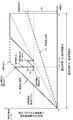
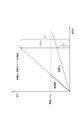
- FIG. 1 is a diagram illustrating the characteristics of an image (long exposure image and short exposure image) having two different exposure times generated by the imaging device.
- the horizontal axis represents time (t), and the vertical axis represents the accumulated charge amount (e) in the light receiving photodiode (PD) constituting the photoelectric conversion element corresponding to one pixel of the solid-state imaging element.
- the amount of light received by the light-receiving photodiode (PD) when the amount of light received by the light-receiving photodiode (PD) is large, that is, when the subject corresponds to a bright subject, as shown in the high luminance region 11 shown in FIG.
- the amount of light received by the light-receiving photodiode (PD) when the amount of light received by the light-receiving photodiode (PD) is small, that is, when the object corresponds to a dark subject, the charge accumulation amount gradually increases as time passes, as shown in the low luminance region 12 shown in FIG.
- the time t0 to t3 corresponds to the exposure time TL for acquiring the long-time exposure image. Even when the long exposure time TL is shown, the line shown in the low luminance region 12 is obtained based on the charge accumulation amount (Sa) without the charge accumulation amount reaching the saturation level at the time t3 (unsaturated point Py). An accurate gradation expression can be obtained by the gradation level of the pixel determined using the electric signal.
- the accumulated charge of the light receiving photodiode (PD) is once swept out at a time before reaching the time t3, for example, at a time t1 (charge sweep start point P1) shown in the figure.
- the charge sweeping is performed not to all charges accumulated in the light receiving photodiode (PD) but to an intermediate voltage holding level controlled in the photodiode (PD).
- short-time exposure with exposure time TS (t2 to t3) is performed again. That is, short-time exposure is performed for a period from the short-time exposure start point P2 to the short-time exposure end point P3 shown in the figure.
- a charge accumulation amount (Sb) is obtained by this short-time exposure, and a gradation level of the pixel is determined based on an electric signal obtained based on the charge accumulation amount (Sb).
- Patent Document 2 Japanese Patent Laid-Open No. 2000-50151
- Patent Document 2 takes a plurality of images with different exposure amounts, and compares the plurality of images with different exposure amounts during the composition process.
- a configuration is disclosed in which a pixel region that has moved is identified and corrected to suppress generation of false colors associated with synthesis.
- each of the configurations described in Patent Documents 1 and 2 described above requires processing for individually capturing and combining the long exposure image and the short exposure image.
- a frame memory that holds data for at least one image is required, which causes a problem of increasing costs.
- DSP Digital Signal Processor
- JP 2008-99158 A Japanese Patent Laid-Open No. 2000-50151
- An object of the present invention is to provide an image processing apparatus, an imaging apparatus, an image processing method, and a program.
- the first aspect of the present invention is: A control unit that performs exposure time control in units of pixels or pixel areas; A pixel unit that outputs pixel information of a plurality of different exposure times by photographing processing under the control of the control unit; An image processing apparatus having a pixel information composition unit that inputs pixel information of a plurality of different exposure times output from the pixel unit, calculates a pixel value of an output image by executing arithmetic processing using the plurality of pixel information is there.
- control unit performs exposure time control in units of rows of the pixel unit, and the pixel unit obtains pixel information of different exposure times from a plurality of different rows.
- the pixel information combining unit outputs the pixel value of one pixel of the output image by a calculation process using a plurality of pieces of pixel information input from a plurality of different rows.
- the pixel unit outputs high-sensitivity pixel information from a long-time exposure region, outputs low-sensitivity pixel information from a short-time exposure region, and the pixel information combining unit Sets a weight according to subject brightness for high-sensitivity pixel information input from the long-time exposure area and low-sensitivity pixel information input from the short-time exposure area in the pixel value calculation processing of the output image. The added process is executed.
- the pixel information combining unit sets the weight of the high-sensitivity pixel information to zero when the high-sensitivity pixel information input from the long-time exposure region is equal to or greater than a predetermined threshold.
- the pixel value of the output image is calculated by an arithmetic process that is set to a small value and uses only low-sensitivity pixel information input from the short-time exposure area or sets a large weight.
- the pixel information combining unit sets the weight of the low-sensitivity pixel information to zero when the low-sensitivity pixel information input from the short-time exposure region is less than a predetermined threshold.
- the pixel value of the output image is calculated by an arithmetic process that is set to a small value and uses only high-sensitivity pixel information input from the long-time exposure region or sets a large weight.
- the pixel information combining unit is configured to input a high sensitivity input from the long exposure area when low sensitivity pixel information input from the short exposure area is equal to or greater than a predetermined threshold.
- the pixel value of the output image is calculated by a calculation process in which the weight of the pixel information is set to zero or small and only the low-sensitivity pixel information input from the short-time exposure region is used or the weight is set large.
- control unit performs exposure time control in which a long exposure region and a short exposure region are set in units of two rows of the pixel unit, and the pixel unit Outputs at least one or more pieces of pixel information from each of the long-time exposure region and the short-time exposure region, and the pixel information combining unit outputs high-sensitivity pixel information input from the long-time exposure region and short-time exposure.
- the pixel value of one pixel of the output image is calculated by arithmetic processing using at least one or more pieces of pixel information input from each of the low sensitivity pixel information input from the region.
- control unit executes exposure time control in units of rows by shutter control in units of rows of the pixel units.
- control unit performs exposure time control in color units by shutter control in color units of the pixel units.
- the image processing device further includes a counter that counts a digital value corresponding to a pixel value of a high-sensitivity pixel in a long-time exposure region output from the pixel unit.
- a counter that counts a digital value corresponding to a pixel value of a high-sensitivity pixel in a long-time exposure region output from the pixel unit.
- an output selection unit that selectively outputs the pixel value of the low-sensitivity pixel in the short-time exposure region of the same color as the high-sensitivity pixel as the pixel value for calculation of the output image.
- the pixel unit outputs high-sensitivity pixel information from a long-time exposure region, outputs low-sensitivity pixel information from a short-time exposure region, and performs the long-time exposure.
- Medium sensitivity pixel information is output from a medium-time exposure region that is an exposure time between short-time exposures, and the pixel information combining unit is configured to calculate the high-sensitivity pixel information and the low-sensitivity pixels in the pixel value calculation process of the output image.
- a weight corresponding to the subject brightness is set in the information and medium sensitivity pixel information, and calculation processing is executed to calculate the pixel value of the output image.
- the image processing device further includes a tone conversion unit that performs a bit reduction process of the pixel value of each pixel of the output image generated by the pixel information synthesis unit.
- the image processing apparatus further includes a signal processing unit that executes signal processing on the output image generated by the pixel information combining unit.
- the image processing apparatus further includes a codec that executes an encoding process on the output image generated by the pixel information combining unit.
- the pixel unit is configured to output pixel information of the same color and different exposure times from an area of 3 ⁇ 3 pixel area or more.
- the pixel section has a Bayer array or an RGBW array.
- the second aspect of the present invention provides An imaging unit; It exists in an imaging device which has an image process part which performs the process in any one of Claims 1-16.
- the third aspect of the present invention provides An image processing method executed in an image processing apparatus, A control step in which the control unit executes exposure time control in units of pixels or pixel areas; and A pixel unit that outputs pixel information of a plurality of different exposure times by photographing processing under the control of the control unit; and A pixel information combining step in which a pixel information combining unit inputs pixel information of a plurality of different exposure times output from the pixel unit, executes a calculation process using the plurality of pixel information, and calculates a pixel value of an output image In the image processing method.
- the fourth aspect of the present invention provides A program for executing image processing in an image processing apparatus; A control step for causing the control unit to perform exposure time control in units of pixels or pixel areas; and A pixel information output step for causing the pixel unit to output pixel information of a plurality of different exposure times by photographing processing under the control of the control unit; A pixel information combining step for inputting pixel information of a plurality of different exposure times output from the pixel unit to the pixel information combining unit and calculating a pixel value of an output image by executing arithmetic processing using the plurality of pixel information It is in the program that executes
- the program of the present invention is a program that can be provided by, for example, a storage medium or a communication medium that is provided in a computer-readable format to an information processing apparatus or a computer system that can execute various program codes.
- a program in a computer-readable format, processing corresponding to the program is realized on the information processing apparatus or the computer system.
- system is a logical set configuration of a plurality of devices, and is not limited to one in which the devices of each configuration are in the same casing.
- an apparatus and a method for generating a wide dynamic range image based on one captured image are realized. Specifically, exposure time control is performed to set different exposure times for each pixel area, such as a row unit of the pixel portion, and a plurality of different pixel information that are pixel values of pixels set to different exposure times are acquired. For example, high-sensitivity pixel information is acquired from the long-time exposure pixels, and low-sensitivity pixel information is acquired from the short-time exposure pixels, and the pixel value of the output image is calculated based on the pixel information of these different sensitivities.
- the weight of the low sensitivity pixel information is set to be large, and in the low luminance region, it is estimated that the SN ratio of the low sensitivity pixel information is bad.
- the output pixel value is determined by setting a high weight for the high sensitivity pixel information.
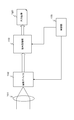
- FIG. 2 is a block diagram illustrating a configuration of an imaging apparatus which is an example of the image processing apparatus of the present invention.
- the light incident through the optical lens 101 is incident on an imaging device 102 configured by, for example, a CMOS image sensor, and outputs image data by photoelectric conversion.
- the output image data is input to the signal processing unit 103.
- the signal processing unit 103 performs signal processing in a general camera, such as white balance (WB) adjustment and gamma correction, and generates an output image 120.
- the output image 120 is stored in a storage unit (not shown). Or it outputs to a display part.
- WB white balance
- the control unit 105 outputs a control signal to each unit according to a program stored in a memory (not shown), for example, and performs various processing controls.
- a program stored in a memory (not shown), for example, and performs various processing controls.
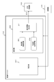
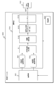
- the imaging device 102 according to the first embodiment includes a pixel unit 201 and a calculation unit 202 as illustrated in FIG.
- the pixel unit 201 outputs charge information corresponding to the exposure time by photoelectric conversion in each pixel of a pixel array of a Bayer array including RGB pixels, for example.
- the pixel unit 201 is set to a different exposure time for each pixel region (for example, for each row (line)) under the control of the control unit 105 (shutter control).
- High-sensitivity pixel information 251 corresponding to stored electrification based on long-time exposure is output from a row subjected to long-time exposure.
- low-sensitivity image information 252 corresponding to storage electrification based on short-time exposure is output from a row subjected to short-time exposure.
- a specific example of the control structure of the exposure time will be described in detail later. Note that a control unit may be set in the imaging device, and processing control in the imaging device may be executed by control of the control unit in the imaging device.
- the calculation unit 202 includes a pixel information composition unit 211 that receives the high-sensitivity pixel information 251 and the low-sensitivity image information 252 output from the pixel unit 201 and generates one piece of image information based on the input information.
- the output of the pixel information combining unit 211 is input to the signal processing unit 103.
- the signal processing unit 103 performs signal processing in a general camera, such as white balance (WB) adjustment and gamma correction, and generates an output image 120.
- the output image 120 is stored in a storage unit (not shown). Or it outputs to a display part.
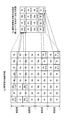
- FIG. 4 is a diagram illustrating an example of a combining process executed in the pixel information combining unit of the imaging device according to the first embodiment of the present invention.
- FIG. (A) Captured image of the pixel unit
- both (a) and (b) are diagrams showing only a partial region of a captured image or a pixel information composite image.
- the color filter array of the pixel unit 201 is a Bayer array, and has a configuration in which R, Gb, Gr, and B pixels are set according to a specified array.
- the pixel information combining unit 211 of the calculation unit 202 of the imaging device 102 in FIG. 3 combines a plurality of pieces of pixel information in the pixel unit 201 illustrated in FIG. 4A to generate a pixel information combined image illustrated in FIG. It is generated and output to the signal processing unit 103 at the next stage.
- FIG. 4 shows a processing example in which the pixel value of one pixel of the output image is determined from a total of four pixels having different sensitivities, that is, two high-sensitivity pixels and two low-sensitivity pixels. That is, in this embodiment, the pixel information combining unit 211 determines the pixel value of one pixel of the output image based on the four pixels included in the image captured by the pixel unit 201. By this processing, an output image having a number of pixels that is 1/4 of the number of pixels in the pixel portion is generated and output.
- the pixel value of the upper left pixel Gb (out) of the output image generated by the pixel information combining unit 211 illustrated in FIG. 4B is 4 in the upper left portion of the pixel unit 201 that is the captured image illustrated in FIG. It is calculated based on the pixel values of two pixels, that is, Gb (0, 0), Gb (1, 0), Gb (0, 1), Gb (1, 1), and these four pixels.
- a high-sensitivity pixel region and a low-sensitivity pixel region are alternately set in units of two rows.
- the high-sensitivity pixel area is an area that is exposed for a long time
- the low-sensitivity pixel area is an area where short-time exposure is performed.
- exposure time control is performed in units of rows of the pixel unit 201 as described above, and an image in which high-sensitivity pixel regions and low-sensitivity pixel regions are alternately set is captured in units of two rows.
- the pixel information synthesis unit 211 inputs the pixel value of the pixel in the high sensitivity pixel region and the pixel value of the pixel in the low sensitivity region, and determines the pixel value of one output pixel.
- the pixel information combining unit 211 converts the pixel value of the upper left pixel Gb (out) of the pixel information combined image of FIG. 4B to the upper left four pixels of the captured image of FIG.
- High-sensitivity pixels Gb (0, 0), Gb (1, 0)
- Low sensitivity pixels Gb (0, 1), Gb (1, 1)
- Calculation is based on the pixel values of these two high-sensitivity pixels and two low-sensitivity pixels.
- the pixel information combining unit 211 performs a similar pixel value calculation process for all the pixels of the pixel information combined image in FIG. 4B, that is, Gb (out), Gr (out), B (out), R (out ). That is, the pixel values of all these output images are calculated using the pixel values of the two high sensitivity pixels and the two low sensitivity pixels of the captured image in FIG.
- the degree of contribution (distribution ratio) of the pixel values of the four input pixels is not constant, and for example, processing such as determination depending on the brightness of the subject is performed. This process will be described later.
- FIG. 4 shows an example in which the high-sensitivity pixel region and the low-sensitivity pixel region are alternately set in units of two rows, but this is an example, and the unit for switching the pixel region is other than two rows. It is good also as a setting.
- Gb (out) [Gb (0,0) ⁇ ⁇ ] + [Gb (1,0) ⁇ ⁇ ] + [Gb (0,1) ⁇ (Gain) ⁇ ⁇ ] + [Gb (1,1) ⁇ (Gain) ⁇ ⁇ ] ...
- Gb (x, y) is a pixel value at the (x, y) coordinate position of the captured image
- Gain Gain value that compensates for the sensitivity ratio (default value)
- the pixel information combining unit 211 includes a plurality of pixels including at least a high-sensitivity pixel and a low-sensitivity pixel from a plurality of pixels of the input image at a position corresponding to the pixel position of the output image illustrated in FIG. A value is input, and each pixel value of the pixel information composite image shown in FIG. 4B is calculated according to the above formula.
- pixel values of two high sensitivity pixels and two low sensitivity pixels are input, and each pixel value of the pixel information composite image shown in FIG. 4B is calculated according to the above formula.
- the same pixel value calculation process as in (Expression 1) is executed. That is, the pixel value of Gr (out) of the output image of FIG. 4B is the two Gr pixels of the high sensitivity pixel region in the pixel region of the captured image corresponding to the pixel position of Gr (out) of the pixel information composite image. The value is calculated using two Gr pixel values of the low sensitivity pixel region.
- the pixel value of R (out) of the output image in FIG. 4B is the two R pixel values of the high sensitivity pixel region in the pixel region of the captured image corresponding to the pixel position of R (out) of the pixel information composite image. Calculation is performed using two R pixel values in the low sensitivity pixel region.
- the pixel value of B (out) of the output image in FIG. 4B is the two B pixel values of the high sensitivity pixel region in the pixel region of the captured image corresponding to the pixel position of B (out) of the pixel information composite image. Calculation is performed using two B pixel values in the low sensitivity pixel region.
- FIG. 5 is a diagram for explaining gain control.
- the gain from the low-sensitivity pixel is increased by giving a gain four times that of the output from the low-sensitivity pixel. Match the output of the pixel.
- [Alpha], [beta], [gamma], and [epsilon] in the above (Equation 1) are coefficients for setting the contribution of each pixel as described above.
- ⁇ , ⁇ , ⁇ , and ⁇ different values may be used for the colors of the output pixels, for example, Gb, Gr, B, and R, respectively.
- the setting may be changed according to the brightness of the subject.
- the pixel value of a high-sensitivity pixel may be saturated, that is, the maximum pixel value, and an accurate pixel value may not be reflected.
- the pixel value of the output pixel Gb (out) is calculated by applying only the pixel values of Gb (0, 1) and Gb (1, 1) of the low sensitivity pixel. By such processing, the output pixel value can be set using only the effective pixel value information of the low sensitivity pixel without being affected by the pixel value of the saturated high sensitivity pixel.
- the Gain value in the above (Equation 1) and the set values of ⁇ , ⁇ , ⁇ , ⁇ corresponding to the brightness of the subject, or calculation processing algorithms for these values are defined in advance and stored in the memory in the imaging apparatus. Store it. Alternatively, it is implemented as hardware.
- the pixel information synthesis unit 211 obtains or calculates a Gain value and coefficients: ⁇ , ⁇ , ⁇ , ⁇ by applying a memory stored value, hardware, or an algorithm, for example, and outputs an output value according to (Equation 1), that is, The pixel value of the constituent pixel of the pixel information composite image is calculated.
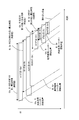
- FIG. 6 is a diagram illustrating an example of controlling the exposure time of the high sensitivity pixel region and the low sensitivity pixel region of the pixel unit 201.
- the vertical axis in FIG. 6 indicates the pixel row of the pixel portion, and the horizontal axis indicates the elapsed time.
- the time on the horizontal axis indicates that the time has elapsed as it proceeds in the right direction.
- FIG. 6 shows an example of processing for controlling the exposure time of the high-sensitivity pixel region and the low-sensitivity pixel region when the sensitivity ratio of low-sensitivity pixels: high-sensitivity pixels is 1: 4.
- the exposure time of the high sensitivity pixel is set to four times the exposure time of the low sensitivity pixel.
- the exposure time of the electronic shutter is controlled in units of rows in order to set the high sensitivity pixel area and low sensitivity pixel area.
- a CMOS imager used as the pixel unit 201 of the imaging device 102 illustrated in FIG. 3 has a configuration capable of electronic shutter control in units of rows. That is, it is a configuration in which an arbitrary exposure time can be set for each row. For example, row-by-row exposure time control is executed based on a control signal output from the control unit 105 shown in FIG. 3 to the pixel unit 201 of the imaging device 102.
- the exposure time control example shown in FIG. 6 is an exposure corresponding to a configuration in which a high-sensitivity pixel region and a low-sensitivity pixel region are alternately set in units of two rows as shown on the left side of the captured image of the pixel portion in FIG. It is an example of time control.
- the first row and the second row are high-sensitivity pixel regions that are subjected to long-time exposure processing.
- the third row and the fourth row are low-sensitivity pixel regions that are subjected to short-time exposure processing.
- a high-sensitivity pixel region in which long-time exposure processing is executed in units of two rows and a low-sensitivity pixel region in which short-time exposure processing is executed are alternately set.
- the exposure starts from the upper row to the lower row sequentially from the shutter start (exposure start) time t1 of the first row. Is done.
- the right-downward dotted line (E1) at the right end of FIG. 6 indicates the read start (exposure end) position of the charge accumulated in each pixel.
- This pixel value reading process is performed on all rows without distinction between high-sensitivity pixel rows (1, 2, 5, 6,...) And low-sensitivity pixel rows (3,4, 7, 8,). Executed about. Reading of the first row is started at time t3, and for the second, third, fourth, fifth, sixth, seventh,... Rows, the pixel values (accumulation) of all the rows toward the lower row as time elapses. (Charge) is read out.
- the shutter control shown in FIG. 6 is as follows. Set the exposure start time of high-sensitivity pixel rows (1, 2, 5, 6,%) Earlier (t1), The exposure start time of the low-sensitivity pixel rows (3, 4, 7, 8,%) Is set with a delay (t2). Further, readout (exposure end) is sequentially executed from the upper row from time (t3). By this processing, the exposure time of the high sensitivity pixel rows (1, 2, 5, 6,%) Is longer than the exposure time of the low sensitivity pixel rows (3, 4, 7, 8,). In the example, 4 times) is set, and accumulated charges (pixel values) based on different exposure times can be acquired from each pixel.
- the length of the exposure time is changed every two rows. The longer the exposure time, the higher the sensitivity, and the shorter the exposure time, the lower the sensitivity.
- FIG. 7 is a diagram for explaining an example of a process for generating a composite image generated by the pixel information combining unit 211 as a result of the exposure control shown in FIG. 6, that is, a pixel information composite image.
- the pixel information combining unit 211 illustrated in FIG. 3 applies the pixel values of a plurality of pixels, and outputs one of the output images illustrated in FIG. The pixel value of the pixel is determined.
- the coefficients in the above formulas: ⁇ , ⁇ , ⁇ , and ⁇ may be set to change according to the brightness of the subject, for example.
- the pixel value of a high-sensitivity pixel may be saturated, that is, the maximum pixel value, and an accurate pixel value may not be reflected.
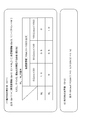
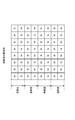
- FIG. 7 shows three processing modes for such a processing mode. That is, (1) Bright subject (high sensitivity pixels are saturated) (2) Medium subject (high-sensitivity pixel is less than saturation value, both high-sensitivity pixel and low-sensitivity pixel are above the preset allowable SN ratio) (3) Dark subject (high-sensitivity pixel is less than saturation value and low-sensitivity pixel is less than the predetermined allowable SN ratio) It is a figure explaining the aspect of the synthetic
- the pixel value of the high sensitivity pixel is not applied to the pixel value calculation of the output pixel of the pixel information composite image.
- a process of calculating an output pixel value by applying only the pixel value of Gb (1, 1) is executed.
- the pixel value of the high sensitivity pixel: Gb (0, 0), Gb (1, 0) is not used, and the pixel value of the low sensitivity pixel: Gb (0, 1) Gb (1, 1) only. Is applied to calculate the output pixel value of the pixel information composite image.
- an average value of two low-sensitivity pixels may be set as a pixel value of one output pixel in the pixel information composite image.
- an average value of a total of four pixels of two high-sensitivity pixels and two low-sensitivity pixels may be set as the pixel value of one output pixel in the pixel information composite image.
- the pixel values of the low-sensitivity pixels: Gb (0, 1) Gb (1, 1) are not used, and the pixel values of the high-sensitivity pixels: Gb (0, 0), Gb (1, 0) only Is applied to calculate the output pixel value of the pixel information composite image.
- an average value of two high-sensitivity pixels may be set as a pixel value of one output pixel in the pixel information composite image.
- the pixel information synthesis unit 211 determines whether to use a high-sensitivity pixel or a low-sensitivity pixel depending on the brightness of the subject when determining each pixel value of the pixel information synthesis image to be generated. , You will decide whether to use both. If it is bright, the high-sensitivity pixel may be saturated (invalid). In this case, it is preferable to use the information of the low-sensitivity pixel as it is, but when both pieces of pixel information are valid, which one is used. Or it is better to decide in consideration of the SN ratio.
- FIG. 8 is one sequence example of the process executed by the pixel information combining unit 211.
- pixel value calculation of the pixel information composite image is executed in the following sequence.
- step S11 an intermediate composite pixel value based on two vertical pixels is calculated.
- step S12 pixel value calculation of an image to be finally output is executed using intermediate composite pixel values based on two vertical pixels.
- step S11 only one high-sensitivity pixel and one low-sensitivity pixel are selected to calculate an intermediate composite pixel value, and then in step S12, the final result is based on these intermediate composite pixel values.
- the pixel value of the image to be output is calculated.
- FIG. 9A shows an example of operations and coefficients applied to the process of calculating intermediate composite pixel values based on the two vertical pixels in step S11 of FIG.
- FIG. 9B shows an example of calculation applied to the final pixel value calculation process based on two intermediate composite pixel values in step S12 of FIG.
- Equation 2 is one intermediate composition executed in step S11 of FIG. 8 in the calculation process of the pixel value: Gb (out) of the pixel information composition image described above with reference to FIG.
- the calculation formula of pixel value [Gb (1)] is shown.
- Gb (x, y) is a pixel value at the (x, y) coordinate position of the captured image
- Gain Gain value that compensates for the sensitivity ratio (default value)
- W H a weighting factor corresponding to the high sensitivity pixel of the input pixel
- W L Weight coefficient corresponding to the low sensitivity pixel of the input pixel
- the multiplication factor for the pixel values of the low-sensitivity pixels the W L
- the multiplication factor for the pixel values of the high-sensitivity pixel the W H as 1, intermediate dependent only on the pixel values of the high-sensitivity pixels
- the pixel value [Gb (1)] of the combined pixel is calculated.
- the multiplication factor for the pixel values of the low-sensitivity pixels the W L as 0.5
- the multiplication factor for the pixel values of the high-sensitivity pixel W H as 0.5
- high-sensitivity pixels and low-sensitivity two pixel values of the pixels The pixel value [Gb (1)] of the intermediate combined pixel is calculated by the average of the above.
- the multiplication factor for the pixel values of the high-sensitivity pixel the W H
- the multiplication factor for the pixel values of the low-sensitivity pixels the W L as 1, intermediate dependent only on the pixel values of the low-sensitivity pixels
- the pixel value [Gb (1)] of the combined pixel is calculated.
- the coefficient can be set using the low sensitivity pixel information.
- three types are used for simplification, but a function for calculating a weight based on low-sensitivity pixel information is set in advance, and the low-sensitivity inputted by the pixel information combining unit 211 shown in FIG.
- a configuration may be adopted in which the coefficients W H and W L are calculated by executing an operation to which a predetermined function is applied based on the pixel information 252.
- FIG. 9 shows an example of calculation applied to the process of step S12 in FIG. 8, that is, the final pixel value calculation process based on two intermediate composite pixel values.
- the calculation executed as the final pixel value calculation process based on the intermediate combined pixel value in step S12 in FIG. 8 is as follows.
- Output [Gb (out)] [Gb (1) ⁇ 0.5] + [Gb (2) ⁇ 0.5] (Formula 4)
- Equation 4 is the two intermediate synthesis executed in step S12 of FIG. 8 in the calculation process of the pixel value: Gb (out) of the pixel information synthesis image described above with reference to FIG.
- the calculation formula of the final pixel value calculation process based on a pixel value is shown.
- an example in which final pixel value calculation is performed by a simple average of two intermediate composite pixel values is shown.
- the pixel value calculation processing example of the pixel information composite image described with reference to FIGS. 8 and 9 is an example.
- a coefficient that compensates for the deviation of the center of gravity due to addition is set when the weighting coefficient is set.
- Various processes are possible.
- a weighting coefficient applied to calculation of each pixel of the pixel information composite image for example, W H 1 and W L may be calculated separately, but a configuration may be used in which the calculated weight values of the neighboring pixels that have been processed in advance are used.
- FIG. 10 is a diagram for describing a processing example in the case where the Gb pixel of the output image is calculated in advance in the pixel information combining unit, and then the B pixel is calculated.
- Coefficients W H1 and W L1 shown in the calculation formula of the output [Gb (1)] are coefficients set according to the coefficient setting mode described with reference to FIG. 9 (1).
- the coefficients W H2 and W L2 shown in the calculation formula for the output [Gb (2)] are also coefficients set in accordance with the coefficient setting mode described with reference to FIG.
- the coefficients used for calculating the B pixel in the pixel information composite image that is, the weighting coefficient for multiplying the pixel B (p) and the pixel B (q) shown in FIG.
- the calculation formula for the intermediate composite pixel value B (1) of B is the following calculation formula.
- Output [B (1)] [B (p) ⁇ W Hb + [B (q) ⁇ (Gain) ⁇ W Lb ]
- Such a calculation formula is obtained.
- W Hb and W Lb used in this equation are calculated as follows, for example.
- W Hb (W H1 + W H2 ) / 2
- W Lb (W L1 + W L2 ) / 2
- the B weighting coefficient may be calculated based on the Gb coefficient.
- the process of stabilizing the weighting coefficient without greatly changing depending on the color of each pixel of the output image results in increasing the contribution of pixel information of either high sensitivity or low sensitivity depending on the color of each pixel of the output image. It is stabilized without greatly changing depending on the color. This leads to equalization and stabilization of the exposure time of the pixel area in the output image, and as a result, it contributes to preventing the generation of false colors due to deviations in the exposure period when the object being photographed moves.
- FIG. 11 is a diagram illustrating a configuration example of the imaging device 300 according to the second embodiment of the present invention.
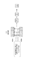
- the imaging device 300 includes a pixel unit 301, an output selection unit 302, and a calculation unit 303 as shown in the figure.
- the output selection unit 302 is configured as individual output selection units 302a, 302b... For the output pixels from each column of the pixel unit 301.
- Each output selection unit includes a comparator 321 and a counter. 322 and determination unit 323 are included.
- the calculation unit 303 includes a pixel information synthesis unit 311.
- the control signal from the control unit 105 shown in FIG. 2 is input to the pixel unit 301, the output selection unit 302, and the calculation unit 303, and various controls are executed.
- the configuration and processing of the pixel unit 301 are the same as those in the first embodiment.
- a high-sensitivity pixel row that is exposed for a long time and a low-sensitivity pixel row that is exposed for a short time are set in units of two rows.
- the exposure processing is performed by the same shutter control as described with reference to FIG. 6 as in the first embodiment, and high-sensitivity pixel rows that are subjected to long-time exposure in units of two rows and short-time exposure are performed.
- a low sensitivity pixel row is set.
- the readout sequence of the accumulated charges after exposure is different from that in the first embodiment.
- the rows 2, 3, 4, 5,... are read from the first row in order from the top.
- the reading order is set as follows. 1st row (high sensitivity pixel row), 3rd row (low sensitivity pixel row), Second row (high sensitivity pixel row) 4th row (low sensitivity pixel row), 5th row (high sensitivity pixel row) 7th row (low sensitivity pixel row), 6th row (high sensitivity pixel row) : as mentioned above, A process of alternately reading high sensitivity pixel rows and low sensitivity pixel rows from above is executed.
- the pixel values (accumulated charges) read out in this way are sequentially output to the comparator 321 of the output selection unit 302.
- the high-sensitivity pixel value and low-sensitivity pixel value of the same color are sequentially input to the comparator 321 in each column.
- the counter 322 first counts the digital value of the high sensitivity pixel input from the comparator 321 in advance.
- the determination unit 323 determines whether the digital value of the high-sensitivity pixel input from the comparator 321 in advance is 512 or more, which is a half value of 10 bits (0 to 1032). When the digital value of the high sensitivity pixel is 512 or more, the high sensitivity pixel information, that is, the digital data indicating the pixel value of the high sensitivity pixel is discarded (initialized).
- the low sensitivity pixel is read, and pixel information of the low sensitivity pixel is input to the counter 322 as a digital value. Thereafter, this digital value is output.
- the counter 322 holds the high-sensitivity pixel information as it is and does not overwrite it with the information of the low-sensitivity pixel.
- the high-sensitivity pixel may be saturated, and the S / N ratio of the low-sensitivity pixel information is good.
- the high sensitivity pixel information is discarded and the low sensitivity pixel information is input to the counter 322.
- the digital value of the high-sensitivity pixel is less than 512, there is no possibility that the high-sensitivity pixel is saturated, and the high-sensitivity pixel information is counted according to the judgment that the SN ratio of the low-sensitivity pixel information is bad. 322 is held as it is.
- the threshold value for determining which to select is described as a half pixel value, but the threshold value is determined by the performance of the image sensor or the like.
- the pixel information is selected in the comparator 321, the counter 322, and the determination unit 323 as the output selection unit constituting the AD conversion circuit unit, and then the pixel information in the horizontal direction is the same as in the first embodiment described above.
- the vertical direction may be selected within the image sensor, and the horizontal direction may be processed by an LSI outside the image sensor.
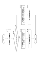
- the flowchart shown in FIG. 13 is a flowchart for explaining the sequence of pixel value selection processing in the imaging device 300 according to the second embodiment of the present invention shown in FIG. First, in step S ⁇ b> 101, the comparator 321 generates digital data of pixel values of high sensitivity pixels read from the pixel unit 301 in advance.
- the flow shown in FIG. 13 is described as an example of the Gb pixel reading process.
- step S102 the counter 322 counts the digital data of the pixel value of the high sensitivity pixel input from the comparator 321, and determines whether it is less than 512, which is half of 10 bits (0 to 1023).
- step S103 When the digital data of the pixel value of the high sensitivity pixel is less than 512, the process proceeds to step S103, and when it is 512 or more, the process proceeds to step S105.
- step S103 the digital data of the pixel value of the high sensitivity pixel is held, and the pixel value of the low sensitivity pixel of the same color as the next input value So that it is not overwritten with data corresponding to.
- step S104 the digital value of the pixel value of the high sensitivity pixel is output.
- step S102 determines whether the digital data of the pixel value of the high sensitivity pixel is 512 or more. If it is determined in step S102 that the digital data of the pixel value of the high sensitivity pixel is 512 or more, the process proceeds to step S105, the pixel value corresponding data of the high sensitivity pixel is discarded, and the next input value is obtained. A digital value corresponding to the pixel value of the low-sensitivity pixel of the same color is held. In step S106, a digital value of the pixel value of the low sensitivity pixel is output.
- the pixel value of the high-sensitivity pixel of the same color and the pixel value of the low-sensitivity pixel are successively read out from the pixel unit, and the pixel value of the high-sensitivity pixel read out in advance is a predetermined threshold value (for example If it is less than half of the maximum value), the pixel value of the high sensitivity pixel is selected and output. If the pixel value of the high sensitivity pixel is equal to or greater than a prescribed threshold value (for example, half the maximum value), the low sensitivity pixel Are selectively output.
- This process realizes a configuration in which a pixel value of a low sensitivity pixel is selectively output in a bright pixel region, and a pixel value of a high sensitivity pixel is selectively output in a relatively dark region. Is rejected, and the pixel value of the output pixel can be determined by selecting a highly accurate pixel value.
- FIG. 14 is a diagram illustrating a configuration of the imaging device 400 according to the third embodiment.
- the configuration shown in FIG. 14 is a configuration in which a gradation conversion unit 412 is provided after the imaging device shown in FIG.
- Other configurations are the same as those of the first embodiment shown in FIG.
- the overall configuration of the image processing apparatus has the configuration described above with reference to FIG.
- the pixel unit 401 has a Bayer array including, for example, the RGbGrB pixels described in the first embodiment with reference to FIG. 4 and is controlled in units of two rows under the control of the control unit 105.
- the long exposure and the short exposure are executed at The exposure sequence is performed according to the sequence shown in FIG.
- the pixel unit 401 is set to a different exposure time for each pixel region (for example, row (line) unit) under the control of the control unit 105 (shutter control), and accumulation based on long-time exposure is performed from a row subjected to long-time exposure.
- High-sensitivity pixel information 451 that is electrification is output.
- low-sensitivity image information 452 that is stored electrification based on short-time exposure is output from a row that is subjected to short-time exposure.
- the calculation unit 402 receives the high-sensitivity pixel information 451 and the low-sensitivity image information 452 output from the pixel unit 401, and generates one pixel information combined image in the pixel information combining unit 411 based on these input information. .
- This synthesizing process is performed as the same process as the synthesizing process described in the first embodiment with reference to FIG. 4 and FIGS.
- the high-sensitivity pixel information and the low-sensitivity pixel information of the same color are input, and the pixel value calculation of the pixel information composite image is performed by applying (Equation 1) or (Equation 2) to (Equation 4) described above. Execute to generate a pixel information composite image.
- a gradation converting unit 412 is provided after the pixel information combining unit 411.
- the gradation conversion unit 412 converts the gradation of the pixel value of each pixel of the pixel information combined image (for example, FIG. 4B) generated by the pixel information combining unit 411. Specifically, for example, when the pixel value of each pixel of the pixel information combined image generated by the pixel information combining unit 411 has a gradation of 14 bits (0 to 16383), the pixel value of each pixel is set to 10 bits (0 to 1023). Performs processing to convert to gradation and output. That is, an image in which the number of bits of each pixel is reduced is generated and output.
- a wide dynamic range image generated by combining a long-exposure image and a short-exposure image tends to increase the number of bits as information of each pixel.
- the number of bits is 14 bits.
- Such an image with an increased number of bits may not be processed by a DSP, which is a subsequent signal processing unit.
- the gradation conversion unit 412 executes a gradation conversion process that compresses the number of bits of each pixel to a bit level that can be processed by a DSP that is a subsequent signal processing unit.
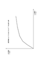
- bit number compression processing executed by the gradation conversion unit 412 will be described with reference to FIG.
- the horizontal axis indicates the gradation [14 bits (0 to 16383) of each pixel of the input image of the gradation conversion unit 412
- the vertical axis indicates the gradation [10 bits (0 to 1023) of each pixel in the output image after the gradation conversion. ]].
- the gradation conversion unit 412 performs a process of reducing the multi-tone pixel value output from the pixel information combining unit 411 to a smaller number of bits.
- the signal processing unit 103 can perform processing without any problem.
- the bit number compression processing executed by the gradation conversion unit 412 reduces the number of bits using, for example, a function. This function may be determined from the beginning, or a function corresponding to an image may be input from the outside or calculated internally.
- Example 4 Next, as Example 4 of the present invention, after the tone conversion unit described in Example 3, a signal processing unit that executes camera signal processing such as demosaic or noise reduction (NR), or image compression (JPEG or the like) processing is performed.
- camera signal processing such as demosaic or noise reduction (NR), or image compression (JPEG or the like) processing is performed.
- NR demosaic or noise reduction
- JPEG image compression
- FIG. 16 is a diagram illustrating a configuration of the imaging device 500 according to the fourth embodiment.
- the configuration shown in FIG. 16 includes a signal processing unit 513 that executes camera signal processing such as demosaic and noise reduction (NR) after the imaging device shown in FIG. 3 described as the first embodiment, and image compression (such as JPEG).
- the configuration includes a codec 514 that executes processing.
- the overall configuration of the image processing apparatus is the same as that of the first embodiment, the configuration described above with reference to FIG. 2, or the configuration in which the signal processing unit 103 is omitted from the configuration in FIG.
- the processing executed by the signal processing unit 103 having the configuration shown in FIG. 2 is all executed by the signal processing unit 513 shown in FIG. 16, the subsequent signal processing unit 103 can be omitted.
- a configuration including two signal processing units may be employed.
- the pixel unit 501 has a Bayer array including, for example, RGbGrB pixels described in the first embodiment with reference to FIG. 4, and is controlled in units of two rows under the control of the control unit 520.
- the long exposure and the short exposure are executed at The exposure sequence is performed according to the sequence shown in FIG.
- the control unit 520 is shown as a bag set in the imaging device.
- the pixel unit 501 is set to a different exposure time for each pixel area (for example, row (line) unit) under the control of the control unit 520 (shutter control), and accumulation based on long-time exposure is performed from a row subjected to long-time exposure.
- High-sensitivity pixel information 551 that is electrification is output.
- low-sensitivity image information 552, which is stored electrification based on short-time exposure is output from a row that is subjected to short-time exposure.
- the calculation unit 502 receives the high-sensitivity pixel information 551 and the low-sensitivity image information 552 output from the pixel unit 501, and generates one pixel information combined image in the pixel information combining unit 511 based on these input information. .
- This synthesizing process is performed as the same process as the synthesizing process described in the first embodiment with reference to FIG. 4 and FIGS.
- the high-sensitivity pixel information and the low-sensitivity pixel information of the same color are input, and the pixel value calculation of the pixel information composite image is performed by applying (Equation 1) or (Equation 2) to (Equation 4) described above. Execute to generate a pixel information composite image.
- a signal processing unit 513 that executes camera signal processing such as demosaic and noise reduction (NR), and an image A codec 514 that executes compression (such as JPEG) processing is provided.
- NR demosaic and noise reduction
- JPEG compression
- Example 5 a new example of exposure control of a pixel portion in an imaging device will be described.
- a high-sensitivity pixel region that performs long-time exposure processing in units of two rows in the pixel unit, and a low-sensitivity pixel that performs short-time exposure processing. It was set as the structure which sets an area
- the fifth embodiment does not set the exposure time fixed in such a row unit, but performs a long exposure process or a color signal (R, Gr, Gb, B) unit in each row based on the control signal. It is the Example made into the structure which can be set to any conversion of a short time exposure process.
- FIG. 17 illustrates a configuration example of the pixel portion of the imaging device according to the present embodiment.
- two control lines are connected to each of the constituent pixels (R, Gr, Gb, B) of the pixel portion. These are the control signal A and control signal B lines.
- control signals are control signals input from the control unit, and as shown in FIG. In the odd rows of the first, third, fifth ... Control signals A1, A3, A5... Are connected to Gb pixels, Control signals B1, B3, B5... Are connected to the B pixel. Also, In the second, fourth, sixth ... Control signals A2, A4, A6... Are connected to the R pixel, Control signals B2, B4, B6... Are connected to the Gr pixel.
- each control line is configured to be used as a control signal for only one color.
- a color-compatible control signal connection configuration is described in, for example, non-patent literature [ISSCC 2006 Dig. tech. Papers, pp. 492-493 (2)], and by using this description structure, each pixel can be controlled by a control signal.
- exposure time control corresponding to each color is executed by a control signal corresponding to each color.
- Any of the control signals A1 to An and B1 to Bn shown in FIG. 17 can be set by the control unit 105 (see FIG. 3), and various exposure times can be set.
- the exposure time can be changed for each color, not limited to the two exposure time settings of the long exposure and the short exposure. That is, it becomes possible to control each color unit of the pixel portion, and it is possible to generate an output image in which the optimum sensitivity is selected for each color.
- FIG. 18 is a diagram corresponding to the exposure time control example described above with reference to FIG. 6 in the first embodiment.
- the vertical axis indicates the pixel row of the pixel portion, and the horizontal axis indicates the elapsed time.
- the example shown in FIG. Set the first long exposure time and the first short exposure time of Gb, R, Set a second long exposure time for Gr, B and a second short exposure time, This is an example in which the long exposure time and short exposure time set for Gb and R and the long exposure time and short exposure time set for Gr and B are changed.
- a Gb, R color pair and a Gr, B color pair are set, and two colors of one pair have the same exposure time combination, but each of R, Gr, Gb, B It is also possible to change the setting of the long exposure time and the short exposure time. As described above, when this embodiment is applied, it is possible to control each color unit of the pixel unit, and it is possible to generate an output image in which an optimum sensitivity is selected for each color.
- FIG. 19 illustrates a configuration example of the pixel unit in the imaging device according to the sixth embodiment.
- the pixel arrangement (array structure) shown in FIG. 19 is an arrangement obtained by rotating the arrangement of the pixel portion described in Embodiment 1 with reference to FIG. 4A by 45 degrees.
- the exposure time control in units of rows is performed on the array shown in FIG. As shown in FIG.
- the first row is a row composed of Gb and Gr pixels
- the second row is a row composed of B and R pixels
- the third, fourth, fifth ... A row composed of Gb and Gr pixels;
- FIG. 20 shows an example of exposure control and composition processing in the imaging device of the seventh embodiment.
- FIG. 20 is a view similar to FIG. 4 of the first embodiment described above.
- both (a) and (b) are diagrams showing only a partial region of a captured image or a pixel information composite image.
- a high-sensitivity pixel region that executes long-time exposure processing and a low-sensitivity pixel region that executes short-time exposure processing are set in units of two rows in the pixel portion.
- Example 7 as shown in FIG. High-sensitivity pixel areas where the first and second lines are exposed for a long time, Medium sensitivity pixel area where the 3rd to 4th lines perform medium time exposure, 5th to 6th rows are low-sensitivity pixel areas where short-time exposure is performed,
- the high sensitivity pixel region, the medium sensitivity pixel region, and the low sensitivity pixel region are repeated in units of two rows.
- the imaging device configuration of the present embodiment has the configuration shown in FIG.
- the pixel information combining unit inputs three high-sensitivity pixels, medium-sensitivity pixels, and low-sensitivity pixels of the same color, and outputs one pixel of the pixel information composite image based on a total of nine pixel values. The pixel value of is determined.
- the pixel information combining unit calculates a pixel value Gb (out) of one pixel of the pixel information combined image based on the pixel values of these nine pixels.
- the pixel information combining unit calculates the pixel value of Gb (out) shown in FIG. 20B according to the following equation (Equation 1).
- Gb (out) [Gb (0,0) ⁇ k1] + [Gb (1,0) ⁇ k2] + [Gb (2,0) ⁇ k3] + [Gb (0,1) ⁇ (Gain1) ⁇ k4] + [Gb (1,1) ⁇ (Gain1) ⁇ k5] + [Gb (2,1) ⁇ (Gain1) ⁇ k6] + [Gb (0,2) ⁇ (Gain2) ⁇ k7] + [Gb (1,2) ⁇ (Gain2) ⁇ k8] + [Gb (2,2) ⁇ (Gain2) ⁇ k9] ...
- Gb (x, y) is a pixel value at the (x, y) coordinate position of the captured image
- Gain1, Gain2 Gain values (predetermined values) for compensating the sensitivity ratio
- the coefficients k1 to k9 are set by, for example, processing such as setting values according to the brightness of the subject.
- nine pixel values including a high sensitivity pixel, a medium sensitivity pixel, and a low sensitivity pixel included in the captured image are used for the calculation processing of the pixel value of one pixel of the pixel information composite image.
- pixel values having three levels of sensitivity it is possible to calculate an optimal pixel value according to brightness, for example.
- the pixel array shown in FIG. 21 has an RGBW pixel array.
- W indicates transparency (white).
- the high sensitivity pixel and the low sensitivity pixel, each of which inputs two total 4 pixels, are calculated according to the above-described (Equation 1).
- the 3 ⁇ 3 pixel region shown in FIG. 21 includes only one high-sensitivity pixel and one low-sensitivity pixel, respectively.
- the output pixel value of the pixel information composite image is calculated based on the pixel value of the low sensitivity pixel.
- the pixel information combining process using the RGBW arrangement at least one pixel of high sensitivity pixels and one of low sensitivity pixels is input, and pixel information having these different sensitivities is applied to the pixel information.
- the pixel value of the composite image is determined. For example, when the subject is bright and the high-sensitivity pixel has a saturation value, the pixel value of the pixel information composite image is set using the pixel value of the low-sensitivity pixel, the subject is dark, and the SN ratio of the pixel value of the low-sensitivity pixel is poor In this case, processing such as blending by using a pixel value of a high-sensitivity pixel or setting a larger weight is performed.
- Such processing makes it possible to generate and output a wide dynamic range image in which more accurate pixel values are set.
- the series of processes described in the specification can be executed by hardware, software, or a combined configuration of both.
- the program recording the processing sequence is installed in a memory in a computer incorporated in dedicated hardware and executed, or the program is executed on a general-purpose computer capable of executing various processing. It can be installed and run.
- the program can be recorded in advance on a recording medium.
- the program can be received via a network such as a LAN (Local Area Network) or the Internet and installed on a recording medium such as a built-in hard disk.
- system is a logical set configuration of a plurality of devices, and the devices of each configuration are not limited to being in the same casing.
- an apparatus and a method for generating a wide dynamic range image based on one captured image are realized. Specifically, exposure time control is performed to set different exposure times for each pixel area, such as a row unit of the pixel portion, and a plurality of different pixel information that are pixel values of pixels set to different exposure times are acquired. For example, high-sensitivity pixel information is acquired from the long-time exposure pixel, and low-sensitivity pixel information is acquired from the short-time exposure pixel, and the pixel value of the output image is calculated based on the pixel information of these different sensitivities.
- the weight of the low sensitivity pixel information is set to be large, and in the low luminance region, it is estimated that the SN ratio of the low sensitivity pixel information is bad.
- the output pixel value is determined by setting a high weight for the high sensitivity pixel information.
Landscapes
- Engineering & Computer Science (AREA)
- Multimedia (AREA)
- Signal Processing (AREA)
- Physics & Mathematics (AREA)
- Spectroscopy & Molecular Physics (AREA)
- Studio Devices (AREA)
- Transforming Light Signals Into Electric Signals (AREA)
- Image Processing (AREA)
Abstract
Description
画素または画素領域単位の露光時間制御を実行する制御部と、
前記制御部の制御下での撮影処理によって複数の異なる露光時間の画素情報を出力する画素部と、
前記画素部の出力する複数の異なる露光時間の画素情報を入力し、該複数の画素情報を利用した演算処理を実行して出力画像の画素値を算出する画素情報合成部を有する画像処理装置にある。
撮像部と、
請求項1から16いずれかに記載の処理を実行する画像処理部を有する撮像装置にある。
画像処理装置において実行する画像処理方法であり、
制御部が、画素または画素領域単位の露光時間制御を実行する制御ステップと、
画素部が、前記制御部の制御下での撮影処理によって複数の異なる露光時間の画素情報を出力する画素情報出力ステップと、
画素情報合成部が、前記画素部の出力する複数の異なる露光時間の画素情報を入力し、該複数の画素情報を利用した演算処理を実行して出力画像の画素値を算出する画素情報合成ステップを実行する画像処理方法にある。
画像処理装置において画像処理を実行させるプログラムであり、
制御部に、画素または画素領域単位の露光時間制御を実行させる制御ステップと、
画素部に、前記制御部の制御下での撮影処理によって複数の異なる露光時間の画素情報を出力させる画素情報出力ステップと、
画素情報合成部に、前記画素部の出力する複数の異なる露光時間の画素情報を入力し、該複数の画素情報を利用した演算処理を実行して出力画像の画素値を算出させる画素情報合成ステップを実行させるプログラムにある。
これらの処理により、1つの撮影画像に基づく広ダイナミックレンジ画像の生成が実現される。
1.画像処理装置の全体構成例について
2.画像処理装置の具体的構成と処理の実施例について
(2-1.実施例1)
~
(2-8.実施例8)
まず、本発明の画像処理装置の全体構成例について図2を参照して説明する。
図2は、本発明の画像処理装置の一例である撮像装置の構成を示すブロック図である。光学レンズ101を通して入射される光は例えばCMOSイメージセンサなどによって構成される撮像デバイス102に入射し、光電変換による画像データを出力する。出力画像データは信号処理部103に入力される。信号処理部103は、例えばホワイトバランス(WB)調整、ガンマ補正等、一般的なカメラにおける信号処理を実行して出力画像120を生成する。出力画像120は図示しない記憶部に格納される。あるいは表示部に出力される。
以下、撮像デバイスの構成と処理を中心として、複数の実施例について説明する。
(2-1.実施例1)
まず、本発明の画像処理装置の実施例1に係る撮像デバイスの構成と処理について説明する。
実施例1の撮像デバイス102は、図3に示すように画素部201と、演算部202を有する。
画素部201は、例えばRGB画素からなるベイヤー配列の画素配列の各画素における光電変換によって、露光時間に応じた電荷情報を出力する。本実施例1の構成において、画素部201は制御部105の制御(シャッタ制御)により、画素領域単位(例えば行(ライン)単位)で異なる露光時間に設定される。長時間露光のなされる行からは長時間露光に基づく蓄積電化に対応する高感度画素情報251が出力される。また、短時間露光のなされる行からは短時間露光に基づく蓄積電化に対応する低感度画像情報252を出力する。露光時間の制御構成の具体例については後段で詳細に説明する。なお、撮像デバイス内に制御部を設定し、撮像デバイスにおける処理制御は、撮像デバイス内の制御部の制御によって実行する構成としてもよい。
図4には、
(a)画素部の撮影画像
(b)画素情報合成部の合成処理によって生成される出力画像
これらを示している。
なお、(a),(b)とも撮影画像あるいは画素情報合成画像の一部領域のみを示した図である。
すなわち、本実施例において画素情報合成部211は画素部201において撮影される画像に含まれる4画素に基づいて、出力画像の1画素の画素値を決定する。この処理により、画素部の画素数の1/4の画素数の出力画像を生成して出力する。
高感度画素領域は、長時間露光を行う領域であり、
低感度画素領域は、短時間露光を行う領域である。
本実施例の構成では、このように、画素部201の行単位で露光時間制御を行い、2行単位で高感度画素領域と、低感度画素領域を交互に設定した画像を撮影する。画素情報合成部211は、これら高感度画素領域中の画素の画素値と、低感度領域中の画素の画素値を入力して1つの出力画素の画素値を決定する。
高感度画素:Gb(0,0)、Gb(1,0)と、
低感度画素:Gb(0,1)、Gb(1,1)、
これら2つの高感度画素と2つの低感度画素の画素値に基づいて算出する。
図4(b)に示すGb(out)の画素値は例えば以下の式(式1)に従って算出する。
Gb(out)=[Gb(0,0)×α]+[Gb(1,0)×β]+[Gb(0,1)×(Gain)×γ]+[Gb(1,1)×(Gain)×ε]
・・・・・(式1)
ただし、
Gb(x,y)は、撮影画像の(x,y)座標位置における画素値、
Gain:感度比を補償するゲイン値(既定値)、
α,β,γ,ε:入力画素の寄与度を設定する係数であり、α+β+γ+ε=1の関係を満たす係数、
である。
すなわち、図4(b)の出力画像のGr(out)の画素値は、画素情報合成画像のGr(out)の画素位置に対応する撮影画像の画素領域における高感度画素領域の2つのGr画素値と低感度画素領域の2つのGr画素値を利用して算出する。
図4(b)の出力画像のR(out)の画素値は、画素情報合成画像のR(out)の画素位置に対応する撮影画像の画素領域における高感度画素領域の2つのR画素値と低感度画素領域の2つのR画素値を利用して算出する。
図4(b)の出力画像のB(out)の画素値は、画素情報合成画像のB(out)の画素位置に対応する撮影画像の画素領域における高感度画素領域の2つのB画素値と低感度画素領域の2つのB画素値を利用して算出する。
例えば、低感度画素:高感度画素の感度比が1:4である場合、低感度画素からの出力には4倍のゲインを与え、上記式(式1)において、
Gain=4.0
として設定する。
これにより、明るさに対する線形性が保たれ、ワイドダイナミックレンジを実現することができる。
低感度画素:高感度画素の感度比が1:4である場合、図5に示すように、低感度画素からの出力に対して4倍のゲインを与えて、低感度画素の出力を高感度画素の出力と整合させる。
例えば、上記(式1)において、
α=β=0として、高感度画素のGb(0,0)とGb(1,0)の画素値を適用せず、
γ+ε=1として、低感度画素のGb(0,1)とGb(1,1)の画素値のみを適用して出力画素値を算出する処理を実行する。
Gb(out)=[Gb(0,0)×α]+[Gb(1,0)×β]+[Gb(0,1)×(Gain)×γ]+[Gb(1,1)×(Gain)×ε]
=[Gb(0,1)×(Gain)×γ]+[Gb(1,1)×(Gain)×ε]
として、
出力画素の画素値:Gb(out)を、低感度画素のGb(0,1)とGb(1,1)の画素値のみを適用して算出する。
このような処理により、飽和した高感度画素の画素値の影響を受けずに、低感度画素の有効画素値情報のみを用いて出力画素値を設定することができる。
図6の縦軸が画素部の画素行を示し、横軸が経過時間を示している。縦軸の行は、最上部が画素部の第1行であり、以下、下に向かって下位の行(行番号=2,3,4,5・・・)となる。
横軸の時間は、右方向に進むに従って時間が経過していることを示す。
本例において、高感度画素の露光時間は低感度画素の露光時間の4倍に設定される。
1行目と2行目とが長時間の露光処理がなされる高感度画素領域となる。
3行目と4行目とが短時間の露光処理がなされる低感度画素領域となる。
以下の5行目以降も2行単位で長時間露光処理が実行される高感度画素領域と、短時間露光処理が実行される低感度画素領域が交互に設定される。
1行目と2行目、5行目と6行目等の高感度画素領域では、第1行のシャッタ開始(露光開始)時間t1から、順次、上位行から下位行に向かって露光が開始される。時間t1からの右下がり点線(S1)が高感度画素行(行番号=1,2,5,6,・・・)の各行のシャッタ開始(露光開始)位置を示している。なお、シャッタの開閉動作は、上位行から順次、下位行に向けて実行されるので、下位行に進むに従って処理時間が遅れる。この影響でラインが右下がりに設定される。
高感度画素行(1,2,5,6,・・・)の露光開始時間を早め(t1)に設定し、
低感度画素行(3,4,7,8,・・・)の露光開始時間を遅れて(t2)設定する。
さらに、読み出し(露光終了)を時間(t3)から上位行から順次実行する。
この処理により、高感度画素行(1,2,5,6,・・・)の露光時間を、低感度画素行(3,4,7,8,・・・)の露光時間より長く(本例では4倍)設定し、各画素から異なる露光時間に基づく蓄積電荷(画素値)を取得することを可能としている。
(式1)や図4を参照して説明したように、図3に示す画素情報合成部211は、複数の画素の画素値を適用して、図4(b)に示す出力画像の1つの画素の画素値を決定する。
Gb(out)=[Gb(0,0)×α]+[Gb(1,0)×β]+[Gb(0,1)×(Gain)×γ]+[Gb(1,1)×(Gain)×ε]
上記式に従って、撮影画像の複数の画素値から1つの画素値を算出する。
(1)明るい被写体(高感度画素が飽和値)
(2)中位の被写体(高感度画素が飽和値以下で、高感度画素、低感度画素とも既定の許容SN比以上)
(3)暗い被写体(高感度画素が飽和値以下で、低感度画素が既定の許容SN比未満)
これらの被写体の撮影領域に対応する合成処理の態様を説明する図である。
(1)明るい被写体(高感度画素が飽和値)
図7(1)に示すように被写体が明るく、高感度画素が飽和値である場合は、高感度画素の画素値は、画素部の各画素において蓄積可能な最大電荷量に対応する最大画素値となり、正確な画素値を反映できない状態にある。
すなわち、α=β=0として、高感度画素のGb(0,0)とGb(1,0)の画素値を適用せず、γ+ε=1として、低感度画素のGb(0,1)とGb(1,1)の画素値のみを適用して出力画素値を算出する処理を実行する。
Gb(out)=[Gb(0,0)×α]+[Gb(1,0)×β]+[Gb(0,1)×(Gain)×γ]+[Gb(1,1)×(Gain)×ε]
=[Gb(0,1)×(Gain)×γ]+[Gb(1,1)×(Gain)×ε]
上記のように、高感度画素の画素値:Gb(0,0),Gb(1,0)を利用せず、低感度画素の画素値:Gb(0,1)Gb(1,1)のみを適用して画素情報合成画像の出力画素値を算出する。
α=β=0
γ+ε=1
上記制約を満たす範囲で、様々な設定が可能である。一例として、例えば、
γ=ε=0.5
このような設定として、低感度画素2画素の平均値を画素情報合成画像における1つの出力画素の画素値として設定してもよい。
図7(2)に示すように、明るさが中位の被写体、すなわち、高感度画素が飽和値以下で、高感度画素、低感度画素とも既定の許容SN比以上である場合は以下の処理を行う。
高感度画素、低感度画素とも正確な画素値を反映していると判断できるため、どちらかを選択して利用して画素情報合成画像の画素値として設定してもよいし、すべてを利用したブレンド処理を実行して画素情報合成画像の画素値を算出してもよい。
α+β+γ+ε=1
上記制約を満たす範囲で、様々な設定が可能である。一例として、例えば、
α=β=γ=ε=0.25
このような設定として、高感度画素2画素と低感度画素2画素の計4画素の平均値を画素情報合成画像における1つの出力画素の画素値として設定してもよい。
図7(3)に示すように、暗い被写体、すなわち、高感度画素が飽和値以下で、低感度画素が既定の許容SN比未満である場合は以下の処理を行う。
低感度画素の画素値は、予め定めた許容SN比未満であり、正確な画素値を反映していると言えない。このような場合は、低感度画素の画素値を適用せず、高感度画素の画素値のみに基づいて画素情報合成画像の出力画素値を算出する。
γ=ε=0
α+β=1
とする。
すなわち、例えば、図4におけるGb(out)の算出処理において、
Gb(out)=[Gb(0,0)×α]+[Gb(1,0)×β]+[Gb(0,1)×(Gain)×γ]+[Gb(1,1)×(Gain)×ε]
=[Gb(0,0)×α]+[Gb(1,0)×β]
上記のように、低感度画素の画素値:Gb(0,1)Gb(1,1)を利用せず、高感度画素の画素値:Gb(0,0),Gb(1,0)のみを適用して画素情報合成画像の出力画素値を算出する。
α+β=1
上記制約を満たす範囲で、様々な設定が可能である。一例として、例えば、
α=β=0.5
このような設定として、高感度画素2画素の平均値を画素情報合成画像における1つの出力画素の画素値として設定してもよい。
図8に示す処理は、画素情報合成部211の実行する処理の1つのシーケンス例である。図8に示す例では、以下のシーケンスで画素情報合成画像の画素値算出を実行している。
次に、ステップS12において、縦方向の2画素に基づく中間的な合成画素値同士を利用して最終的に出力する画像の画素値算出を実行する。
図9(1)には、図8のステップS11における縦方向の2画素に基づく中間的な合成画素値を算出する処理に適用する演算と係数の例を示している。
図9(2)には、図8のステップS12における2つの中間的な合成画素値に基づく最終的な画素値算出処理に適用する演算例を示している。
出力[Gb(1)]=[Gb(0,0)×WH]+[Gb(0,1)×(Gain)×WL]
・・・・・(式2)
出力[Gb(2)]=[Gb(1,0)×WH]+[Gb(1,1)×(Gain)×WL]
・・・・・(式3)
Gb(x,y)は、撮影画像の(x,y)座標位置における画素値、
Gain:感度比を補償するゲイン値(既定値)、
WH:入力画素の高感度画素に対応する重み係数、
WL:入力画素の低感度画素に対応する重み係数、
ただし、WH+WL=1の関係を満たす係数、
である。
ここでは、低感度画素の画素値に応じて、異なる係数を利用する設定としている。
具体的には、例えば図9(1)に示す以下の設定の係数を利用する。
なお、各画素の画素値は10bit(0~1023)の出力であるとする。
低感度画素の画素値(data)に応じて以下の設定とする。
(a)0≦data<50の場合:WH=1.0、WL=0
(b)50≦data<100の場合:WH=0.5、WL=0.5
(c)100≦data<1023の場合:WH=0、WL=1.0
(a)0≦data<50の場合
このように、低感度画素の画素値(data)が小さい場合、被写体の明るさが低く、低感度画素の画素値のSN比が低いと推定される。この場合、低感度画素の画素値(data)の信頼度が低いと判断され、また、近傍の高感度画素の画素値が飽和していないと推定される。このような場合は、低感度画素の画素値に対する乗算係数:WLを0として、高感度画素の画素値に対する乗算係数:WHを1として、高感度画素の画素値のみに依存した中間的な合成画素の画素値[Gb(1)]を算出する。
このように、低感度画素の画素値(data)が中程度である場合、被写体の明るさが中程度であり、低感度画素の画素値のSN比が良好であると推定される。この場合、低感度画素の画素値(data)の信頼度が高いと判断され、また、近傍の高感度画素の画素値も飽和していないと推定される。このような場合は、低感度画素の画素値と高感度画素の画素値をブレンドする。すなわち、低感度画素の画素値に対する乗算係数:WLを0.5として、高感度画素の画素値に対する乗算係数:WHも0.5として、高感度画素と低感度画素の2つの画素値の平均により中間的な合成画素の画素値[Gb(1)]を算出する。
このように、低感度画素の画素値(data)が高い場合、被写体の明るさが極めて明るいと判断される。この場合、低感度画素の画素値のSN比は良好であり、低感度画素の画素値(data)の信頼度が高いと判断されるが、近傍の高感度画素の画素値は飽和している可能性が高いと推定される。このような場合は、高感度画素の画素値に対する乗算係数:WHを0として、低感度画素の画素値に対する乗算係数:WLを1として、低感度画素の画素値のみに依存した中間的な合成画素の画素値[Gb(1)]を算出する。
この図9(2)に示すように、図8のステップS12における中間的な合成画素値に基づく最終的な画素値算出処理として実行する演算は、以下のような演算となる。
出力[Gb(out)]=[Gb(1)×0.5]+[Gb(2)×0.5]
・・・・・(式4)
ここでは2つの中間的な合成画素値の単純平均によって、最終的な画素値算出を行う例を示している。
図10に示す例は、画素情報合成部において先行して出力画像のGb画素の算出が実行され、その後にB画素の算出を行う場合の処理例について説明する図である。
出力[Gb(1)]=[Gb(0,0)×WH1+[Gb(0,1)×(Gain)×WL1]
出力[Gb(2)]=[Gb(1,0)×WH2]+[Gb(1,1)×(Gain)×WL2]
出力[Gb(2)]の算出式に示される係数、WH2、WL2も、図9(1)を参照して説明した係数の設定態様に従って設定された係数である。
出力[B(1)]=[B(p)×WHb+[B(q)×(Gain)×WLb]
このような算出式となる。
WHb=(WH1+WH2)/2
WLb=(WL1+WL2)/2
このように、Bの重みづけの係数を、Gbの係数に基づいて算出する構成としてもよい。
次に、本発明の実施例2として、AD変換回路において複数の画素から一つの画素を選択して、選択画素に基づいて出力画像の画素値の設定を行う構成を持つ撮像デバイスの構成と処理例について説明する。
長時間露光がなされる高感度画素行と、短時間露光がなされる低感度画素行とが2行単位で設定される。
露光処理は、実施例1と同様、先に図6を参照して説明したと同様のシャッタ制御によって行われ、2行単位で長時間露光がなされる高感度画素行と、短時間露光がなされる低感度画素行が設定される。
ただし、本処理例では、露光後の蓄積電荷の読み出しシーケンスが、先の実施例1とは異なる。
これに対して、実施例2では、図11に示すように、読み出し順が以下のような設定となる。
第1行(高感度画素行)、
第3行(低感度画素行)、
第2行(高感度画素行)
第4行(低感度画素行)、
第5行(高感度画素行)
第7行(低感度画素行)、
第6行(高感度画素行)
:
上記のように、
高感度画素行と、低感度画素行とを交互に上から読み出す処理を実行する。
まず、高感度画素行である第1行の[Gb(0,0)]が入力され、次に、低感度画素行である第3行の同じ色の[Gb(0,1)]が入力される。
同様に、第2列では、高感度画素行である第1行の[B]が入力され、次に、低感度画素行である第3行の同じ色の[B]が入力される。
このように、コンパレータ321には、各列各々において、同じ色の画素値について、先に高感度画素値が入力され、その後に低感度画素値が入力される。
コンパレータ321は、各画素について、
画素値=0~1023
この範囲のデジタルデータを各画素からの出力電荷量に応じて設定してカウンタ322に出力する。
コンパレータ321は、まず高感度画素の画素値を示すデジタルデータを生成してカウンタ322に出力し、その後、同じ色の低感度画素の画素値を示すデジタルデータをカウンタ322に出力する。
判定部323は、先行してコンパレータ321から入力する高感度画素のデジタル値が10bit(0~1032)の半分の値である512以上となったか否かを判定する。高感度画素のデジタル値が512以上である場合、高感度画素情報、すなわち高感度画素の画素値を示すデジタルデータを破棄(初期化)する。
一方、高感度画素のデジタル値が512未満である場合、高感度画素が飽和している可能性はなく、また、低感度画素情報のSN比が悪いとの判断に従って、高感度画素情報をカウンタ322にそのまま保持させる。
なお、上記説明では、どちらを選択するかの判定閾値を半分の画素値として説明したが、閾値の値は、撮像素子の性能等によって決めることになる。
まず、ステップS101において、コンパレータ321が、先行して画素部301から読み取られる高感度画素の画素値のデジタルデータを生成する。なお、図13に示すフローではGbの画素の読み取り処理例として説明している。
次に、ステップS104に進み、高感度画素の画素値のデジタル値を出力する。
次に、ステップS106に進み、低感度画素の画素値のデジタル値を出力する。
次に、本発明の実施例3として、画素情報合成部の後に、階調変換部を構成した実施例について図14を参照して説明する。
階調変換部412は、画素情報合成部411の生成した画素情報合成画像(例えば図4(b))の各画素の画素値の諧調を変換する。具体的には、例えば画素情報合成部411の生成した画素情報合成画像の各画素の画素値が14bit(0~16383)の諧調を有する場合、各画素の画素値を10bit(0~1023)の諧調に変換して出力するといった処理を行う。すなわち、各画素のビット数を削減した画像を生成して出力する。
なお、階調変換部412の実行するビット数圧縮処理は、例えば関数を利用してビット数を低減する。この関数は最初から決められたものでも良いし、画像に応じた関数を外部から入力もしくは内部で算出してもよい。
次に、本発明の実施例4として、実施例3において説明した諧調変換部の後に、デモザイクやノイズリダクション(NR)といったカメラ信号処理を実行する信号処理部や、画像圧縮(JPEGなど)処理を実行するコーデックを備えた実施例について図16を参照して説明する。
次に、本発明の実施例5として、撮像デバイスにおける画素部の露光制御の新たな実施例について説明する。
先に説明した実施例1では、図4を参照して説明したように、画素部の2行単位で長時間露光処理を実行する高感度画素領域と、短時間露光処理を実行する低感度画素領域を設定する構成としていた。
すなわち、各行は長時間露光または短時間露光のいずれか一方のみの露光処理を固定的に実行する設定となっていた。
図17に示すように、画素部の各構成画素(R,Gr,Gb,B)の各々には、2本の制御をラインが接続されている。制御信号Aと制御信号Bの各ラインである。
第1,3,5,…の奇数行では、
制御信号A1,A3,A5・・・がGb画素に接続され、
制御信号B1,B3,B5・・・がB画素に接続されている。
また、
第2,4,6,…の偶数行では、
制御信号A2,A4,A6・・・がR画素に接続され、
制御信号B2,B4,B6・・・がGr画素に接続されている。
なお、このような色対応の制御信号接続構成については、例えば非特許文献[ISSCC 2006 Dig. tech. Papers, pp.492-493(2)]に記載があり、この記載構成を用いることで各画素に対する制御信号による制御が可能である。
図17に示す制御信号A1~An,B1~Bnのいずれも、制御部105(図3参照)において任意の制御信号の設定が可能であり、様々な露光時間の設定が可能となる。
具体的には、
(1)長時間露光制御のための露光開始と露光終了(読み取り開始)のタイミング制御信号、
(2)短時間露光制御のための露光開始と露光終了(読み取り開始)のタイミング制御信号、
これらの信号のいずれかを制御信号A1~An,B1~Bnに設定することが可能である。
すなわち、画素部の各色単位の制御が可能となり、色毎に最適な感度を選択した出力画像の生成が可能となる。
1~2行、5~6行、9~10行・・が長時間の露光処理がなされる高感度画素領域、
3~4行、7~8行、11~12行・・が短時間の露光処理がなされる低感度画素領域、
このように設定されており、
1つの行に含まれる画素は、すべて同一の露光時間に設定されていた。
Gb,Rの第1の長い露光時間と、第1の短い露光時間を設定し、
Gr,Bの第2の長い露光時間と、第2の短い露光時間を設定し、
Gb,Rに設定する長時間露光時間および短時間露光時間と、Gr,Bに設定する長時間露光時間および短時間露光時間の設定を変えた例である。
このように、本実施例を適用すれば、画素部の各色単位の制御が可能となり、色毎に最適な感度を選択した出力画像の生成が可能となる。
次に、本発明の実施例6として、撮像デバイスにおける画素部の新たな構成例について説明する。
図19に、本実施例6の撮像デバイスにおける画素部の構成例を示す。
図19に示す画素配列(アレイ構造)は、実施例1において図4(a)を参照して説明した画素部の配列を45度回転させた配列となっている。
図19に示すように、
第1行は、Gb,Grの各画素によって構成される行、
第2行は、B,Rの各画素によって構成される行、
以下、第3,4,5…の各行が,
Gb,Grの各画素によって構成される行、
B,Rの各画素によって構成される行、
これらが交互に繰り返される。
GbとGrの組み合わせ、
BとRの組み合わせ、
上記の色画素ペア単位で、露光時間制御を実行することが可能となる。
次に、本発明の実施例7として、撮像デバイスにおける露光制御と画素情報合成部の合成処理の変更例について説明する。
図20に、本実施例7の撮像デバイスにおける露光制御と合成処理例を示す。
(a)画素部の撮影画像
(b)画素情報合成部の合成処理によって生成される出力画像
これらを示している。
なお、(a),(b)とも撮影画像あるいは画素情報合成画像の一部領域のみを示した図である。
この実施例7では、図20(a)に示すように、
第1~2行目が長時間露光を行う高感度画素領域、
第3~4行目が中時間露光を行う中感度画素領域、
第5~6行目が短時間露光を行う低感度画素領域、
以下、2行単位で、高感度画素領域、中感度画素領域、低感度画素領域を繰り返す構成となっている。
画素情報合成部は、例えば、同一色の高感度画素と、中感度画素と、低感度画素とを3つずつ入力し、計9個の画素値に基づいて画素情報合成画像の1つの出力画素の画素値を決定する。
(1)高感度画素:Gb(0,0)、Gb(1,0)、Gb(2,0)、
(2)中感度画素:Gb(0,1)、Gb(1,1)、Gb(2,1)、
(3)低感度画素:Gb(0,2)、Gb(1,2)、Gb(2,2)、
Gb(out)=[Gb(0,0)×k1]+[Gb(1,0)×k2]+[Gb(2,0)×k3]+[Gb(0,1)×(Gain1)×k4]+[Gb(1,1)×(Gain1)×k5]+[Gb(2,1)×(Gain1)×k6]+[Gb(0,2)×(Gain2)×k7]+[Gb(1,2)×(Gain2)×k8]+[Gb(2,2)×(Gain2)×k9]
・・・・・(式5)
ただし、
Gb(x,y)は、撮影画像の(x,y)座標位置における画素値、
Gain1、Gain2:感度比を補償するゲイン値(既定値)、
k1~k9:入力画素の寄与度を設定する係数であり、k1+k2+k3+k4+k5+k6+k7+k8+k9=1の関係を満たす係数、
である。
なお、係数k1~k9の設定は、例えば被写体の明るさに応じた設定値とするなどの処理を行う。
次に、本発明の実施例8として、撮像デバイスにおける画素部の変更例について説明する。
実施例1では、先に図4を参照して説明したように、R,Gr,Gb,Bの各画素から構成されるベイヤー配列を用いた例について説明した。
本発明の画像処理装置は、このベイヤー配列以外の配列からなる画素部を有する構成に対しても対応可能である。図21に示す画素配列はその一例を示す図である。
画像の合成処理に際しては、
W画素とG画素については、先に図4を参照して説明したと同様、高感度画素と低感度画素、それぞれ2つの計4画素を入力して先に説明した(式1)に従って算出する。
ただし、R,B画素については、図21に示す3×3画素領域には、高感度画素と低感度画素がそれぞれ1つずつしか含まれないため、1つの高感度画素の画素値と1つの低感度画素の画素値に基づいて画素情報合成画像の出力画素値を算出する。
これらの処理により、1つの撮影画像に基づく広ダイナミックレンジ画像の生成が実現される。
11 高輝度領域
12 低輝度領域
101 光学レンズ
102 撮像デバイス
103 信号処理部
105 制御部
201 画素部
202 演算部
211 画素情報合成部
251 高感度画素情報
252 低感度画素情報
300 撮像デバイス
301 画素部
302 出力選択部
303 演算部
321 コンパレータ
322 カウンタ
323 判定部
311 画素情報合成部
351 高感度画素情報
352 低感度画素情報
400 撮像デバイス
401 画素部
402 演算部
411 画素情報合成部
412 諧調変換部
451 高感度画素情報
452 低感度画素情報
500 撮像デバイス
501 画素部
502 演算部
511 画素情報合成部
512 諧調変換部
513 信号処理部
514 コーデック
520 制御部
551 高感度画素情報
552 低感度画素情報
Claims (19)
- 画素または画素領域単位の露光時間制御を実行する制御部と、
前記制御部の制御下での撮影処理によって複数の異なる露光時間の画素情報を出力する画素部と、
前記画素部の出力する複数の異なる露光時間の画素情報を入力し、該複数の画素情報を利用した演算処理を実行して出力画像の画素値を算出する画素情報合成部を有する画像処理装置。 - 前記制御部は、前記画素部の行単位で露光時間制御を実行し、
前記画素部は、複数の異なる行から異なる露光時間の画素情報を出力し、
前記画素情報合成部は、複数の異なる行から入力する複数の画素情報を利用した演算処理により出力画像の1つの画素の画素値を算出する請求項1に記載の画像処理装置。 - 前記画素部は、
長時間露光領域から高感度画素情報を出力し、短時間露光領域から低感度画素情報を出力し、
前記画素情報合成部は、
前記出力画像の画素値の算出処理において、
長時間露光領域から入力する高感度画素情報と、短時間露光領域から入力する低感度画素情報とに対して被写体明るさに応じた重みを設定した加算処理を実行する請求項1に記載の画像処理装置。 - 前記画素情報合成部は、長時間露光領域から入力する高感度画素情報が既定の閾値以上である場合、前記高感度画素情報の重みをゼロまたは小さく設定し、短時間露光領域から入力する低感度画素情報のみを利用または重みを大きく設定した演算処理により出力画像の画素値を算出する請求項1に記載の画像処理装置。
- 前記画素情報合成部は、短時間露光領域から入力する低感度画素情報が既定の閾値未満である場合、前記低感度画素情報の重みをゼロまたは小さく設定し、長時間露光領域から入力する高感度画素情報のみを利用または重みを大きく設定した演算処理により出力画像の画素値を算出する請求項1に記載の画像処理装置。
- 前記画素情報合成部は、短時間露光領域から入力する低感度画素情報が既定の閾値以上である場合、長時間露光領域から入力する高感度画素情報の重みをゼロまたは小さく設定し、短時間露光領域から入力する低感度画素情報のみを利用または重みを大きく設定した演算処理により出力画像の画素値を算出する請求項1に記載の画像処理装置。
- 前記制御部は、前記画素部の2行単位で長時間露光領域と短時間露光領域とを設定した露光時間制御を実行し、
前記画素部は、前記長時間露光領域と短時間露光領域の各々から少なくとも1つ以上の画素情報を出力し、
前記画素情報合成部は、前記長時間露光領域から入力する高感度画素情報と、短時間露光領域から入力する低感度画素情報の各々から入力する少なくとも1つ以上の画素情報を利用した演算処理により出力画像の1つの画素の画素値を算出する請求項1に記載の画像処理装置。 - 前記制御部は、
前記画素部の行単位のシャッタ制御により、行単位の露光時間制御を実行する請求項1に記載の画像処理装置。 - 前記制御部は、
前記画素部の色単位のシャッタ制御により、色単位の露光時間制御を実行する請求項1に記載の画像処理装置。 - 前記画像処理装置は、さらに、
前記画素部から出力される長時間露光領域の高感度画素の画素値に相当するデジタル値をカウントするカウンタと、
前記カウンタのカウントする高感度画素の画素値が既定閾値未満である場合、該高感度画素の画素値を前記出力画像の算出用画素値として選択出力し、
前記カウンタのカウントする高感度画素の画素値が既定閾値以上である場合、該高感度画素と同一色の短時間露光領域の低感度画素の画素値を前記出力画像の算出用画素値として選択出力する出力選択部を有する請求項1に記載の画像処理装置。 - 前記画素部は、
長時間露光領域から高感度画素情報を出力し、短時間露光領域から低感度画素情報を出力し、前記長時間露光と短時間露光の間の露光時間である中時間露光領域から中感度画素情報を出力し、
前記画素情報合成部は、
前記出力画像の画素値の算出処理において、
前記高感度画素情報と低感度画素情報と中感度画素情報に、被写体明るさに応じた重みを設定して演算処理を実行して出力画像の画素値を算出する請求項1に記載の画像処理装置。 - 前記画像処理装置は、さらに、
前記画素情報合成部の生成した出力画像の各画素の画素値のビット削減処理を実行する諧調変換部を有する請求項1に記載の画像処理装置。 - 前記画像処理装置は、さらに、
前記画素情報合成部の生成した出力画像に対する信号処理を実行する信号処理部を有する請求項1に記載の画像処理装置。 - 前記画像処理装置は、さらに、
前記画素情報合成部の生成した出力画像に対する符号化処理を実行するコーデックを有する請求項1に記載の画像処理装置。 - 前記画素部は、3×3画素領域以上の領域から同一色の異なる露光時間の画素情報を出力する構成である請求項1に記載の画像処理装置。
- 前記画素部は、ベイヤー配列またはRGBW配列を有する請求項1に記載の画像処理装置。
- 撮像部と、
請求項1から16いずれかに記載の処理を実行する画像処理部を有する撮像装置。 - 画像処理装置において実行する画像処理方法であり、
制御部が、画素または画素領域単位の露光時間制御を実行する制御ステップと、
画素部が、前記制御部の制御下での撮影処理によって複数の異なる露光時間の画素情報を出力する画素情報出力ステップと、
画素情報合成部が、前記画素部の出力する複数の異なる露光時間の画素情報を入力し、該複数の画素情報を利用した演算処理を実行して出力画像の画素値を算出する画素情報合成ステップを実行する画像処理方法。 - 画像処理装置において画像処理を実行させるプログラムであり、
制御部に、画素または画素領域単位の露光時間制御を実行させる制御ステップと、
画素部に、前記制御部の制御下での撮影処理によって複数の異なる露光時間の画素情報を出力させる画素情報出力ステップと、
画素情報合成部に、前記画素部の出力する複数の異なる露光時間の画素情報を入力し、該複数の画素情報を利用した演算処理を実行して出力画像の画素値を算出させる画素情報合成ステップを実行させるプログラム。
Priority Applications (7)
| Application Number | Priority Date | Filing Date | Title |
|---|---|---|---|
| CN2011800532099A CN103190145A (zh) | 2010-11-12 | 2011-10-24 | 图像处理装置、成像装置、图像处理方法和程序 |
| US13/883,696 US9531958B2 (en) | 2010-11-12 | 2011-10-24 | Image processing device, imaging device, image processing method, and program having different exposure start times |
| MX2013005017A MX2013005017A (es) | 2010-11-12 | 2011-10-24 | Aparato de proceso de imagenes, aparato de recopilacion de imagenes, metodo de proceso de imagenes y programa. |
| KR1020137011525A KR20130138360A (ko) | 2010-11-12 | 2011-10-24 | 화상 처리 장치, 촬상 장치 및 화상 처리 방법과 프로그램 |
| CA2812737A CA2812737A1 (en) | 2010-11-12 | 2011-10-24 | Image processing device, imaging device, image processing method, and program |
| BR112013011051A BR112013011051A2 (pt) | 2010-11-12 | 2011-10-24 | dispositivos de processamento e de geração de imagem, método de processamento de imagem, e, programa |
| EP11839426.1A EP2640065A4 (en) | 2010-11-12 | 2011-10-24 | IMAGE PROCESSING DEVICE, IMAGE RECORDING DEVICE, PICTURE PROCESSING PROCESS AND PROGRAM |
Applications Claiming Priority (2)
| Application Number | Priority Date | Filing Date | Title |
|---|---|---|---|
| JP2010254291A JP2012105225A (ja) | 2010-11-12 | 2010-11-12 | 画像処理装置、撮像装置、および画像処理方法、並びにプログラム |
| JP2010-254291 | 2010-11-12 |
Publications (1)
| Publication Number | Publication Date |
|---|---|
| WO2012063634A1 true WO2012063634A1 (ja) | 2012-05-18 |
Family
ID=46050786
Family Applications (1)
| Application Number | Title | Priority Date | Filing Date |
|---|---|---|---|
| PCT/JP2011/074467 Ceased WO2012063634A1 (ja) | 2010-11-12 | 2011-10-24 | 画像処理装置、撮像装置、および画像処理方法、並びにプログラム |
Country Status (9)
| Country | Link |
|---|---|
| US (1) | US9531958B2 (ja) |
| EP (1) | EP2640065A4 (ja) |
| JP (1) | JP2012105225A (ja) |
| KR (1) | KR20130138360A (ja) |
| CN (1) | CN103190145A (ja) |
| BR (1) | BR112013011051A2 (ja) |
| CA (1) | CA2812737A1 (ja) |
| MX (1) | MX2013005017A (ja) |
| WO (1) | WO2012063634A1 (ja) |
Cited By (1)
| Publication number | Priority date | Publication date | Assignee | Title |
|---|---|---|---|---|
| CN106954329A (zh) * | 2016-05-17 | 2017-07-14 | 江苏康众数字医疗设备有限公司 | 成像设备的自动曝光控制方法及曝光系统 |
Families Citing this family (52)
| Publication number | Priority date | Publication date | Assignee | Title |
|---|---|---|---|---|
| JP5896788B2 (ja) * | 2012-03-07 | 2016-03-30 | キヤノン株式会社 | 画像合成装置及び画像合成方法 |
| JP2013219705A (ja) * | 2012-04-12 | 2013-10-24 | Sony Corp | 画像処理装置、および画像処理方法、並びにプログラム |
| US9029753B2 (en) * | 2012-09-27 | 2015-05-12 | National Tsing Hua University | Optical recognition system and method thereof |
| US9113097B2 (en) | 2013-02-06 | 2015-08-18 | Canon Kabushiki Kaisha | Image capturing apparatus that controls performing of short-term and long-term exposures and corresponding read operations, and control method thereof |
| DE102014223858B4 (de) | 2013-11-25 | 2021-09-23 | Canon Kabushiki Kaisha | Bildaufnahmevorrichtung und Bildsignalsteuerverfahren |
| CN103700329B (zh) * | 2013-12-13 | 2015-11-11 | 北京京东方光电科技有限公司 | 显示面板的显示方法 |
| KR102170627B1 (ko) | 2014-01-08 | 2020-10-27 | 삼성전자주식회사 | 이미지 센서 |
| US9307161B2 (en) * | 2014-01-10 | 2016-04-05 | Qualcomm Incorporated | System and method for capturing digital images using multiple short exposures |
| US10104388B2 (en) | 2014-06-30 | 2018-10-16 | Sony Corporation | Video processing system with high dynamic range sensor mechanism and method of operation thereof |
| KR101580178B1 (ko) * | 2014-07-30 | 2015-12-24 | 주식회사 동부하이텍 | 이미지 센서 |
| KR102277178B1 (ko) * | 2015-03-09 | 2021-07-14 | 삼성전자 주식회사 | 카메라 모듈을 포함하는 전자 장치 및 전자 장치의 이미지 처리 방법 |
| JP6521776B2 (ja) * | 2015-07-13 | 2019-05-29 | オリンパス株式会社 | 画像処理装置、画像処理方法 |
| US9819889B2 (en) * | 2015-08-07 | 2017-11-14 | Omnivision Technologies, Inc. | Method and system to implement a stacked chip high dynamic range image sensor |
| CN108174117B (zh) * | 2015-08-10 | 2021-04-02 | Oppo广东移动通信有限公司 | 消除闪烁的方法、系统及移动终端和介质产品 |
| US10298888B2 (en) * | 2015-08-25 | 2019-05-21 | Kabushiki Kaisha Toshiba | Adaptive analyzer of sensitivity difference of same color pixels and adaptive corrector of sensitivity difference of same color pixels |
| CN112714252B (zh) * | 2015-09-30 | 2023-04-07 | 株式会社尼康 | 摄像装置 |
| US20180302552A1 (en) * | 2015-09-30 | 2018-10-18 | Nikon Corporation | Image capturing device and image processing device |
| JP6604384B2 (ja) * | 2015-09-30 | 2019-11-13 | 株式会社ニコン | 撮像装置 |
| CN105611198B (zh) * | 2015-12-18 | 2017-06-27 | 广东欧珀移动通信有限公司 | 图像传感器及具有其的终端 |
| CN105578065A (zh) * | 2015-12-18 | 2016-05-11 | 广东欧珀移动通信有限公司 | 高动态范围图像的生成方法、拍照装置和终端 |
| CN105554419B (zh) * | 2015-12-18 | 2018-04-10 | 广东欧珀移动通信有限公司 | 图像传感器及具有其的终端 |
| CN105578074B (zh) * | 2015-12-18 | 2017-11-10 | 广东欧珀移动通信有限公司 | 图像传感器及具有其的终端 |
| US10313612B2 (en) | 2015-12-18 | 2019-06-04 | Guangdong Oppo Mobile Telecommunications Corp., Ltd. | Image sensor, control method, and electronic device |
| JP6762714B2 (ja) * | 2015-12-28 | 2020-09-30 | ブリルニクス インク | 固体撮像装置およびその駆動方法、電子機器 |
| EP3424403B1 (en) * | 2016-03-03 | 2024-04-24 | Sony Group Corporation | Medical image processing device, system, method, and program |
| WO2017175441A1 (ja) * | 2016-04-06 | 2017-10-12 | ソニー株式会社 | 画像処理装置と画像処理方法 |
| JP6771944B2 (ja) * | 2016-04-27 | 2020-10-21 | キヤノン株式会社 | 撮像装置及び撮像装置の制御方法 |
| KR101823238B1 (ko) * | 2016-05-09 | 2018-01-29 | 삼성전기주식회사 | 이미지 센서 |
| CN106507080B (zh) * | 2016-11-29 | 2018-07-17 | 广东欧珀移动通信有限公司 | 控制方法、控制装置及电子装置 |
| KR102684223B1 (ko) * | 2016-12-12 | 2024-07-11 | 삼성전자주식회사 | 광역 역광 보정 영상 촬상 방법, 이를 수행하는 영상 촬상 장치 및 이를 포함하는 전자 시스템 |
| WO2018123801A1 (ja) * | 2016-12-28 | 2018-07-05 | パナソニック インテレクチュアル プロパティ コーポレーション オブ アメリカ | 三次元モデル配信方法、三次元モデル受信方法、三次元モデル配信装置及び三次元モデル受信装置 |
| JP6827240B2 (ja) * | 2017-03-22 | 2021-02-10 | パナソニックIpマネジメント株式会社 | 画像生成装置、画像生成方法、プログラム及びそれを記録した記録媒体 |
| CN108200354B (zh) * | 2018-03-06 | 2020-09-25 | Oppo广东移动通信有限公司 | 控制方法及装置、成像设备、计算机设备及可读存储介质 |
| JP6833751B2 (ja) * | 2018-03-20 | 2021-02-24 | 株式会社東芝 | 撮像制御装置、撮像装置、及び撮像制御方法 |
| US10554902B2 (en) * | 2018-05-01 | 2020-02-04 | Hanwha Techwin Co., Ltd. | Apparatus and method for processing images |
| JP7130777B2 (ja) * | 2018-06-07 | 2022-09-05 | ドルビー ラボラトリーズ ライセンシング コーポレイション | シングルショットhdrカラーイメージセンサからのhdr画像生成 |
| JP7310098B2 (ja) * | 2018-07-10 | 2023-07-19 | 富士通株式会社 | 赤外線検出器の制御回路及び制御方法、撮像装置 |
| KR20200019432A (ko) * | 2018-08-14 | 2020-02-24 | 에스케이하이닉스 주식회사 | 픽셀 장치 및 그를 이용한 비교 장치와 씨모스 이미지 센서 |
| CN112075072B (zh) | 2018-09-14 | 2024-11-01 | 松下知识产权经营株式会社 | 摄像装置 |
| WO2020054162A1 (ja) * | 2018-09-14 | 2020-03-19 | パナソニックIpマネジメント株式会社 | 撮像装置および撮像方法 |
| US11653101B2 (en) | 2019-05-17 | 2023-05-16 | Samsung Electronics Co., Ltd. | Imaging system for generating high dynamic range image |
| JP2020198470A (ja) | 2019-05-30 | 2020-12-10 | ソニーセミコンダクタソリューションズ株式会社 | 画像認識装置および画像認識方法 |
| JP7217211B2 (ja) * | 2019-08-23 | 2023-02-02 | 日立Astemo株式会社 | 撮像装置及び撮像方法 |
| KR102746170B1 (ko) * | 2019-08-28 | 2024-12-26 | 주식회사 소니 인터랙티브 엔터테인먼트 | 센서 시스템, 화상 처리 장치, 화상 처리 방법 및 프로그램 |
| CN110661982B (zh) * | 2019-09-27 | 2021-08-10 | 思特威(上海)电子科技股份有限公司 | 图像传感器成像中led频闪抑制的方法 |
| JP7547052B2 (ja) * | 2020-02-10 | 2024-09-09 | キヤノン株式会社 | 撮像装置、撮像装置の制御方法、及びプログラム |
| JP7602195B2 (ja) * | 2021-01-27 | 2024-12-18 | オムロン株式会社 | 撮影条件設定システム、撮影条件設定方法及びプログラム |
| KR20220156242A (ko) * | 2021-05-18 | 2022-11-25 | 에스케이하이닉스 주식회사 | 이미지 처리 장치 |
| KR20230015161A (ko) * | 2021-07-22 | 2023-01-31 | 에스케이하이닉스 주식회사 | 촬영 장치 |
| US12380664B2 (en) * | 2021-11-12 | 2025-08-05 | Samsung Electronics Co., Ltd. | Electronic device for generating image and method thereof |
| CN117793540A (zh) * | 2022-09-27 | 2024-03-29 | 华为技术有限公司 | 光敏处理装置和方法 |
| US12627904B2 (en) * | 2024-02-02 | 2026-05-12 | Varjo Technologies Oy | Simultaneous subsampling and high dynamic range imaging in colour filter arrays |
Citations (7)
| Publication number | Priority date | Publication date | Assignee | Title |
|---|---|---|---|---|
| JPH06141229A (ja) * | 1992-10-27 | 1994-05-20 | Matsushita Electric Ind Co Ltd | 高ダイナミックレンジ撮像・合成方法及び高ダイナミックレンジ撮像装置 |
| JP2000050151A (ja) | 1998-07-28 | 2000-02-18 | Olympus Optical Co Ltd | 撮像装置 |
| JP2000069491A (ja) * | 1998-08-19 | 2000-03-03 | Nikon Corp | 撮像素子およびこれを用いた撮像装置 |
| JP2000350222A (ja) * | 1999-06-08 | 2000-12-15 | Fuji Film Microdevices Co Ltd | 固体撮像装置とその制御方法 |
| WO2006049098A1 (ja) * | 2004-11-02 | 2006-05-11 | Matsushita Electric Industrial Co., Ltd. | イメージセンサ |
| JP2007235656A (ja) * | 2006-03-02 | 2007-09-13 | Fujifilm Corp | 固体撮像装置とその駆動方法 |
| JP2008099158A (ja) | 2006-10-16 | 2008-04-24 | Sony Corp | 固体撮像装置、固体撮像装置の駆動方法および撮像装置 |
Family Cites Families (7)
| Publication number | Priority date | Publication date | Assignee | Title |
|---|---|---|---|---|
| US6999119B1 (en) * | 1998-04-10 | 2006-02-14 | Nikon Corporation | Image-capturing element, image-capturing circuit for processing signal from image-capturing element, image-capturing device, driving method of image-capturing element |
| JP2006311240A (ja) * | 2005-04-28 | 2006-11-09 | Olympus Corp | 撮像装置 |
| JP4759363B2 (ja) * | 2005-10-27 | 2011-08-31 | Hoya株式会社 | 画像信号処理ユニット |
| US7825969B2 (en) * | 2006-12-15 | 2010-11-02 | Nokia Corporation | Image stabilization using multi-exposure pattern |
| US8022994B2 (en) * | 2007-08-31 | 2011-09-20 | Omnivision Technologies, Inc. | Image sensor with high dynamic range in down-sampling mode |
| US7940311B2 (en) * | 2007-10-03 | 2011-05-10 | Nokia Corporation | Multi-exposure pattern for enhancing dynamic range of images |
| US8405750B2 (en) * | 2009-06-08 | 2013-03-26 | Aptina Imaging Corporation | Image sensors and image reconstruction methods for capturing high dynamic range images |
-
2010
- 2010-11-12 JP JP2010254291A patent/JP2012105225A/ja active Pending
-
2011
- 2011-10-24 MX MX2013005017A patent/MX2013005017A/es unknown
- 2011-10-24 WO PCT/JP2011/074467 patent/WO2012063634A1/ja not_active Ceased
- 2011-10-24 EP EP11839426.1A patent/EP2640065A4/en not_active Withdrawn
- 2011-10-24 KR KR1020137011525A patent/KR20130138360A/ko not_active Withdrawn
- 2011-10-24 US US13/883,696 patent/US9531958B2/en not_active Expired - Fee Related
- 2011-10-24 BR BR112013011051A patent/BR112013011051A2/pt not_active IP Right Cessation
- 2011-10-24 CN CN2011800532099A patent/CN103190145A/zh active Pending
- 2011-10-24 CA CA2812737A patent/CA2812737A1/en not_active Abandoned
Patent Citations (7)
| Publication number | Priority date | Publication date | Assignee | Title |
|---|---|---|---|---|
| JPH06141229A (ja) * | 1992-10-27 | 1994-05-20 | Matsushita Electric Ind Co Ltd | 高ダイナミックレンジ撮像・合成方法及び高ダイナミックレンジ撮像装置 |
| JP2000050151A (ja) | 1998-07-28 | 2000-02-18 | Olympus Optical Co Ltd | 撮像装置 |
| JP2000069491A (ja) * | 1998-08-19 | 2000-03-03 | Nikon Corp | 撮像素子およびこれを用いた撮像装置 |
| JP2000350222A (ja) * | 1999-06-08 | 2000-12-15 | Fuji Film Microdevices Co Ltd | 固体撮像装置とその制御方法 |
| WO2006049098A1 (ja) * | 2004-11-02 | 2006-05-11 | Matsushita Electric Industrial Co., Ltd. | イメージセンサ |
| JP2007235656A (ja) * | 2006-03-02 | 2007-09-13 | Fujifilm Corp | 固体撮像装置とその駆動方法 |
| JP2008099158A (ja) | 2006-10-16 | 2008-04-24 | Sony Corp | 固体撮像装置、固体撮像装置の駆動方法および撮像装置 |
Non-Patent Citations (2)
| Title |
|---|
| ISSCC 2006 DIG. TECH. PAPERS, 2006, pages 492 - 493 |
| See also references of EP2640065A4 |
Cited By (1)
| Publication number | Priority date | Publication date | Assignee | Title |
|---|---|---|---|---|
| CN106954329A (zh) * | 2016-05-17 | 2017-07-14 | 江苏康众数字医疗设备有限公司 | 成像设备的自动曝光控制方法及曝光系统 |
Also Published As
| Publication number | Publication date |
|---|---|
| CN103190145A (zh) | 2013-07-03 |
| MX2013005017A (es) | 2013-08-01 |
| US20130242152A1 (en) | 2013-09-19 |
| BR112013011051A2 (pt) | 2016-08-23 |
| EP2640065A1 (en) | 2013-09-18 |
| US9531958B2 (en) | 2016-12-27 |
| EP2640065A4 (en) | 2014-05-07 |
| JP2012105225A (ja) | 2012-05-31 |
| CA2812737A1 (en) | 2012-05-18 |
| KR20130138360A (ko) | 2013-12-18 |
Similar Documents
| Publication | Publication Date | Title |
|---|---|---|
| JP2012105225A (ja) | 画像処理装置、撮像装置、および画像処理方法、並びにプログラム | |
| US9288399B2 (en) | Image processing apparatus, image processing method, and program | |
| JP5935876B2 (ja) | 画像処理装置、撮像素子、および画像処理方法、並びにプログラム | |
| WO2013008596A1 (ja) | 画像処理装置、撮像装置、および画像処理方法、並びにプログラム | |
| JP4689620B2 (ja) | イメージセンサ | |
| KR100580911B1 (ko) | 화상합성방법 및 촬상장치 | |
| US9118854B2 (en) | Methods and apparatus for providing optical black compensation of added images | |
| CN101816171B (zh) | 用于增强图像动态范围的多重曝光模式 | |
| US20090290052A1 (en) | Color Pixel Pattern Scheme for High Dynamic Range Optical Sensor | |
| JP2012235332A (ja) | 撮像装置、および撮像装置制御方法、並びにプログラム | |
| JP2013066140A (ja) | 撮像装置、および信号処理方法、並びにプログラム | |
| CN102780849A (zh) | 图像处理装置、图像摄取装置、图像处理方法及程序 | |
| JP2014154982A (ja) | 撮像装置およびその制御方法 | |
| JP4404823B2 (ja) | 撮像装置 | |
| JP2004282552A (ja) | 固体撮像素子および固体撮像装置 | |
| JP2002084449A (ja) | 固体撮像素子を用いた撮像装置 | |
| US20040239790A1 (en) | Image capturing apparatus | |
| JP5612001B2 (ja) | 画像処理装置及び固体撮像装置 | |
| JP4335728B2 (ja) | 画像処理装置および方法 | |
| JP4279562B2 (ja) | 固体撮像装置の制御方法 | |
| JP2004128558A (ja) | 撮像装置 | |
| JP4814749B2 (ja) | 固体撮像装置 | |
| JP2006148591A (ja) | 固体撮像装置および固体撮像素子駆動方法 | |
| JP2013090106A (ja) | 撮像装置及び撮像装置の制御方法 | |
| JP2000299819A (ja) | 撮像装置 |
Legal Events
| Date | Code | Title | Description |
|---|---|---|---|
| 121 | Ep: the epo has been informed by wipo that ep was designated in this application |
Ref document number: 11839426 Country of ref document: EP Kind code of ref document: A1 |
|
| ENP | Entry into the national phase |
Ref document number: 2812737 Country of ref document: CA |
|
| WWE | Wipo information: entry into national phase |
Ref document number: 2011839426 Country of ref document: EP |
|
| ENP | Entry into the national phase |
Ref document number: 20137011525 Country of ref document: KR Kind code of ref document: A |
|
| WWE | Wipo information: entry into national phase |
Ref document number: MX/A/2013/005017 Country of ref document: MX |
|
| WWE | Wipo information: entry into national phase |
Ref document number: 13883696 Country of ref document: US |
|
| NENP | Non-entry into the national phase |
Ref country code: DE |
|
| REG | Reference to national code |
Ref country code: BR Ref legal event code: B01A Ref document number: 112013011051 Country of ref document: BR |
|
| ENP | Entry into the national phase |
Ref document number: 112013011051 Country of ref document: BR Kind code of ref document: A2 Effective date: 20130503 |