WO2012074082A1 - Electrophotographic photosensitive member, process cartridge, electrophotographic apparatus, and method of manufacturing electrophotographic photosensitive member - Google Patents
Electrophotographic photosensitive member, process cartridge, electrophotographic apparatus, and method of manufacturing electrophotographic photosensitive member Download PDFInfo
- Publication number
- WO2012074082A1 WO2012074082A1 PCT/JP2011/077885 JP2011077885W WO2012074082A1 WO 2012074082 A1 WO2012074082 A1 WO 2012074082A1 JP 2011077885 W JP2011077885 W JP 2011077885W WO 2012074082 A1 WO2012074082 A1 WO 2012074082A1
- Authority
- WO
- WIPO (PCT)
- Prior art keywords
- group
- resin
- charge
- photosensitive member
- electrophotographic photosensitive
- Prior art date
- Legal status (The legal status is an assumption and is not a legal conclusion. Google has not performed a legal analysis and makes no representation as to the accuracy of the status listed.)
- Ceased
Links
Classifications
-
- G—PHYSICS
- G03—PHOTOGRAPHY; CINEMATOGRAPHY; ANALOGOUS TECHNIQUES USING WAVES OTHER THAN OPTICAL WAVES; ELECTROGRAPHY; HOLOGRAPHY
- G03G—ELECTROGRAPHY; ELECTROPHOTOGRAPHY; MAGNETOGRAPHY
- G03G5/00—Recording-members for original recording by exposure, e.g. to light, to heat or to electrons; Manufacture thereof; Selection of materials therefor
- G03G5/02—Charge-receiving layers
- G03G5/04—Photoconductive layers; Charge-generation layers or charge-transporting layers; Additives therefor; Binders therefor
- G03G5/043—Photoconductive layers characterised by having two or more layers or characterised by their composite structure
- G03G5/047—Photoconductive layers characterised by having two or more layers or characterised by their composite structure characterised by the charge-generation layers or charge transport layers
-
- G—PHYSICS
- G03—PHOTOGRAPHY; CINEMATOGRAPHY; ANALOGOUS TECHNIQUES USING WAVES OTHER THAN OPTICAL WAVES; ELECTROGRAPHY; HOLOGRAPHY
- G03G—ELECTROGRAPHY; ELECTROPHOTOGRAPHY; MAGNETOGRAPHY
- G03G5/00—Recording-members for original recording by exposure, e.g. to light, to heat or to electrons; Manufacture thereof; Selection of materials therefor
- G03G5/02—Charge-receiving layers
- G03G5/04—Photoconductive layers; Charge-generation layers or charge-transporting layers; Additives therefor; Binders therefor
- G03G5/05—Organic bonding materials; Methods for coating a substrate with a photoconductive layer; Inert supplements for use in photoconductive layers
- G03G5/0528—Macromolecular bonding materials
- G03G5/0589—Macromolecular compounds characterised by specific side-chain substituents or end groups
-
- G—PHYSICS
- G03—PHOTOGRAPHY; CINEMATOGRAPHY; ANALOGOUS TECHNIQUES USING WAVES OTHER THAN OPTICAL WAVES; ELECTROGRAPHY; HOLOGRAPHY
- G03G—ELECTROGRAPHY; ELECTROPHOTOGRAPHY; MAGNETOGRAPHY
- G03G15/00—Apparatus for electrographic processes using a charge pattern
- G03G15/75—Details relating to xerographic drum, band or plate, e.g. replacing, testing
-
- G—PHYSICS
- G03—PHOTOGRAPHY; CINEMATOGRAPHY; ANALOGOUS TECHNIQUES USING WAVES OTHER THAN OPTICAL WAVES; ELECTROGRAPHY; HOLOGRAPHY
- G03G—ELECTROGRAPHY; ELECTROPHOTOGRAPHY; MAGNETOGRAPHY
- G03G5/00—Recording-members for original recording by exposure, e.g. to light, to heat or to electrons; Manufacture thereof; Selection of materials therefor
- G03G5/02—Charge-receiving layers
- G03G5/04—Photoconductive layers; Charge-generation layers or charge-transporting layers; Additives therefor; Binders therefor
- G03G5/05—Organic bonding materials; Methods for coating a substrate with a photoconductive layer; Inert supplements for use in photoconductive layers
-
- G—PHYSICS
- G03—PHOTOGRAPHY; CINEMATOGRAPHY; ANALOGOUS TECHNIQUES USING WAVES OTHER THAN OPTICAL WAVES; ELECTROGRAPHY; HOLOGRAPHY
- G03G—ELECTROGRAPHY; ELECTROPHOTOGRAPHY; MAGNETOGRAPHY
- G03G5/00—Recording-members for original recording by exposure, e.g. to light, to heat or to electrons; Manufacture thereof; Selection of materials therefor
- G03G5/02—Charge-receiving layers
- G03G5/04—Photoconductive layers; Charge-generation layers or charge-transporting layers; Additives therefor; Binders therefor
- G03G5/05—Organic bonding materials; Methods for coating a substrate with a photoconductive layer; Inert supplements for use in photoconductive layers
- G03G5/0528—Macromolecular bonding materials
- G03G5/0557—Macromolecular bonding materials obtained otherwise than by reactions only involving carbon-to-carbon unsatured bonds
- G03G5/056—Polyesters
-
- G—PHYSICS
- G03—PHOTOGRAPHY; CINEMATOGRAPHY; ANALOGOUS TECHNIQUES USING WAVES OTHER THAN OPTICAL WAVES; ELECTROGRAPHY; HOLOGRAPHY
- G03G—ELECTROGRAPHY; ELECTROPHOTOGRAPHY; MAGNETOGRAPHY
- G03G5/00—Recording-members for original recording by exposure, e.g. to light, to heat or to electrons; Manufacture thereof; Selection of materials therefor
- G03G5/02—Charge-receiving layers
- G03G5/04—Photoconductive layers; Charge-generation layers or charge-transporting layers; Additives therefor; Binders therefor
- G03G5/05—Organic bonding materials; Methods for coating a substrate with a photoconductive layer; Inert supplements for use in photoconductive layers
- G03G5/0528—Macromolecular bonding materials
- G03G5/0557—Macromolecular bonding materials obtained otherwise than by reactions only involving carbon-to-carbon unsatured bonds
- G03G5/0564—Polycarbonates
-
- G—PHYSICS
- G03—PHOTOGRAPHY; CINEMATOGRAPHY; ANALOGOUS TECHNIQUES USING WAVES OTHER THAN OPTICAL WAVES; ELECTROGRAPHY; HOLOGRAPHY
- G03G—ELECTROGRAPHY; ELECTROPHOTOGRAPHY; MAGNETOGRAPHY
- G03G5/00—Recording-members for original recording by exposure, e.g. to light, to heat or to electrons; Manufacture thereof; Selection of materials therefor
- G03G5/02—Charge-receiving layers
- G03G5/04—Photoconductive layers; Charge-generation layers or charge-transporting layers; Additives therefor; Binders therefor
- G03G5/05—Organic bonding materials; Methods for coating a substrate with a photoconductive layer; Inert supplements for use in photoconductive layers
- G03G5/0528—Macromolecular bonding materials
- G03G5/0557—Macromolecular bonding materials obtained otherwise than by reactions only involving carbon-to-carbon unsatured bonds
- G03G5/0578—Polycondensates comprising silicon atoms in the main chain
-
- G—PHYSICS
- G03—PHOTOGRAPHY; CINEMATOGRAPHY; ANALOGOUS TECHNIQUES USING WAVES OTHER THAN OPTICAL WAVES; ELECTROGRAPHY; HOLOGRAPHY
- G03G—ELECTROGRAPHY; ELECTROPHOTOGRAPHY; MAGNETOGRAPHY
- G03G5/00—Recording-members for original recording by exposure, e.g. to light, to heat or to electrons; Manufacture thereof; Selection of materials therefor
- G03G5/02—Charge-receiving layers
- G03G5/04—Photoconductive layers; Charge-generation layers or charge-transporting layers; Additives therefor; Binders therefor
- G03G5/06—Photoconductive layers; Charge-generation layers or charge-transporting layers; Additives therefor; Binders therefor characterised by the photoconductive material being organic
-
- G—PHYSICS
- G03—PHOTOGRAPHY; CINEMATOGRAPHY; ANALOGOUS TECHNIQUES USING WAVES OTHER THAN OPTICAL WAVES; ELECTROGRAPHY; HOLOGRAPHY
- G03G—ELECTROGRAPHY; ELECTROPHOTOGRAPHY; MAGNETOGRAPHY
- G03G5/00—Recording-members for original recording by exposure, e.g. to light, to heat or to electrons; Manufacture thereof; Selection of materials therefor
- G03G5/02—Charge-receiving layers
- G03G5/04—Photoconductive layers; Charge-generation layers or charge-transporting layers; Additives therefor; Binders therefor
- G03G5/06—Photoconductive layers; Charge-generation layers or charge-transporting layers; Additives therefor; Binders therefor characterised by the photoconductive material being organic
- G03G5/0601—Acyclic or carbocyclic compounds
- G03G5/0612—Acyclic or carbocyclic compounds containing nitrogen
- G03G5/0614—Amines
- G03G5/06142—Amines arylamine
- G03G5/06144—Amines arylamine diamine
- G03G5/061443—Amines arylamine diamine benzidine
-
- G—PHYSICS
- G03—PHOTOGRAPHY; CINEMATOGRAPHY; ANALOGOUS TECHNIQUES USING WAVES OTHER THAN OPTICAL WAVES; ELECTROGRAPHY; HOLOGRAPHY
- G03G—ELECTROGRAPHY; ELECTROPHOTOGRAPHY; MAGNETOGRAPHY
- G03G5/00—Recording-members for original recording by exposure, e.g. to light, to heat or to electrons; Manufacture thereof; Selection of materials therefor
- G03G5/02—Charge-receiving layers
- G03G5/04—Photoconductive layers; Charge-generation layers or charge-transporting layers; Additives therefor; Binders therefor
- G03G5/06—Photoconductive layers; Charge-generation layers or charge-transporting layers; Additives therefor; Binders therefor characterised by the photoconductive material being organic
- G03G5/0601—Acyclic or carbocyclic compounds
- G03G5/0612—Acyclic or carbocyclic compounds containing nitrogen
- G03G5/0614—Amines
- G03G5/06142—Amines arylamine
- G03G5/06147—Amines arylamine alkenylarylamine
-
- G—PHYSICS
- G03—PHOTOGRAPHY; CINEMATOGRAPHY; ANALOGOUS TECHNIQUES USING WAVES OTHER THAN OPTICAL WAVES; ELECTROGRAPHY; HOLOGRAPHY
- G03G—ELECTROGRAPHY; ELECTROPHOTOGRAPHY; MAGNETOGRAPHY
- G03G5/00—Recording-members for original recording by exposure, e.g. to light, to heat or to electrons; Manufacture thereof; Selection of materials therefor
- G03G5/02—Charge-receiving layers
- G03G5/04—Photoconductive layers; Charge-generation layers or charge-transporting layers; Additives therefor; Binders therefor
- G03G5/06—Photoconductive layers; Charge-generation layers or charge-transporting layers; Additives therefor; Binders therefor characterised by the photoconductive material being organic
- G03G5/0601—Acyclic or carbocyclic compounds
- G03G5/0612—Acyclic or carbocyclic compounds containing nitrogen
- G03G5/0614—Amines
- G03G5/06142—Amines arylamine
- G03G5/06147—Amines arylamine alkenylarylamine
- G03G5/061473—Amines arylamine alkenylarylamine plural alkenyl groups linked directly to the same aryl group
-
- G—PHYSICS
- G03—PHOTOGRAPHY; CINEMATOGRAPHY; ANALOGOUS TECHNIQUES USING WAVES OTHER THAN OPTICAL WAVES; ELECTROGRAPHY; HOLOGRAPHY
- G03G—ELECTROGRAPHY; ELECTROPHOTOGRAPHY; MAGNETOGRAPHY
- G03G5/00—Recording-members for original recording by exposure, e.g. to light, to heat or to electrons; Manufacture thereof; Selection of materials therefor
- G03G5/02—Charge-receiving layers
- G03G5/04—Photoconductive layers; Charge-generation layers or charge-transporting layers; Additives therefor; Binders therefor
- G03G5/06—Photoconductive layers; Charge-generation layers or charge-transporting layers; Additives therefor; Binders therefor characterised by the photoconductive material being organic
- G03G5/0601—Acyclic or carbocyclic compounds
- G03G5/0612—Acyclic or carbocyclic compounds containing nitrogen
- G03G5/0614—Amines
- G03G5/06149—Amines enamine
-
- G—PHYSICS
- G03—PHOTOGRAPHY; CINEMATOGRAPHY; ANALOGOUS TECHNIQUES USING WAVES OTHER THAN OPTICAL WAVES; ELECTROGRAPHY; HOLOGRAPHY
- G03G—ELECTROGRAPHY; ELECTROPHOTOGRAPHY; MAGNETOGRAPHY
- G03G5/00—Recording-members for original recording by exposure, e.g. to light, to heat or to electrons; Manufacture thereof; Selection of materials therefor
- G03G5/02—Charge-receiving layers
- G03G5/04—Photoconductive layers; Charge-generation layers or charge-transporting layers; Additives therefor; Binders therefor
- G03G5/06—Photoconductive layers; Charge-generation layers or charge-transporting layers; Additives therefor; Binders therefor characterised by the photoconductive material being organic
- G03G5/0622—Heterocyclic compounds
- G03G5/0624—Heterocyclic compounds containing one hetero ring
- G03G5/0627—Heterocyclic compounds containing one hetero ring being five-membered
- G03G5/0629—Heterocyclic compounds containing one hetero ring being five-membered containing one hetero atom
-
- G—PHYSICS
- G03—PHOTOGRAPHY; CINEMATOGRAPHY; ANALOGOUS TECHNIQUES USING WAVES OTHER THAN OPTICAL WAVES; ELECTROGRAPHY; HOLOGRAPHY
- G03G—ELECTROGRAPHY; ELECTROPHOTOGRAPHY; MAGNETOGRAPHY
- G03G5/00—Recording-members for original recording by exposure, e.g. to light, to heat or to electrons; Manufacture thereof; Selection of materials therefor
- G03G5/14—Inert intermediate or cover layers for charge-receiving layers
- G03G5/147—Cover layers
-
- G—PHYSICS
- G03—PHOTOGRAPHY; CINEMATOGRAPHY; ANALOGOUS TECHNIQUES USING WAVES OTHER THAN OPTICAL WAVES; ELECTROGRAPHY; HOLOGRAPHY
- G03G—ELECTROGRAPHY; ELECTROPHOTOGRAPHY; MAGNETOGRAPHY
- G03G5/00—Recording-members for original recording by exposure, e.g. to light, to heat or to electrons; Manufacture thereof; Selection of materials therefor
- G03G5/14—Inert intermediate or cover layers for charge-receiving layers
- G03G5/147—Cover layers
- G03G5/14708—Cover layers comprising organic material
- G03G5/14713—Macromolecular material
- G03G5/14747—Macromolecular material obtained otherwise than by reactions only involving carbon-to-carbon unsaturated bonds
- G03G5/14752—Polyesters
-
- G—PHYSICS
- G03—PHOTOGRAPHY; CINEMATOGRAPHY; ANALOGOUS TECHNIQUES USING WAVES OTHER THAN OPTICAL WAVES; ELECTROGRAPHY; HOLOGRAPHY
- G03G—ELECTROGRAPHY; ELECTROPHOTOGRAPHY; MAGNETOGRAPHY
- G03G5/00—Recording-members for original recording by exposure, e.g. to light, to heat or to electrons; Manufacture thereof; Selection of materials therefor
- G03G5/14—Inert intermediate or cover layers for charge-receiving layers
- G03G5/147—Cover layers
- G03G5/14708—Cover layers comprising organic material
- G03G5/14713—Macromolecular material
- G03G5/14747—Macromolecular material obtained otherwise than by reactions only involving carbon-to-carbon unsaturated bonds
- G03G5/14756—Polycarbonates
-
- G—PHYSICS
- G03—PHOTOGRAPHY; CINEMATOGRAPHY; ANALOGOUS TECHNIQUES USING WAVES OTHER THAN OPTICAL WAVES; ELECTROGRAPHY; HOLOGRAPHY
- G03G—ELECTROGRAPHY; ELECTROPHOTOGRAPHY; MAGNETOGRAPHY
- G03G5/00—Recording-members for original recording by exposure, e.g. to light, to heat or to electrons; Manufacture thereof; Selection of materials therefor
- G03G5/14—Inert intermediate or cover layers for charge-receiving layers
- G03G5/147—Cover layers
- G03G5/14708—Cover layers comprising organic material
- G03G5/14713—Macromolecular material
- G03G5/14747—Macromolecular material obtained otherwise than by reactions only involving carbon-to-carbon unsaturated bonds
- G03G5/14773—Polycondensates comprising silicon atoms in the main chain
Definitions
- he present invention relates to an electrophotographic photosensitive member, a process cartridge, an
- An organic electrophotographic photosensitive member (hereinafter, referred to as "electrophotographic photosensitive member") containing an organic charge- generating substance (organic photoconductive
- photosensitive member mounted on an electrophotographic apparatus.
- a variety of members such as a developer, a charging member, a cleaning blade, paper, and a transferring member (hereinafter, also referred to as “contact member or the like") have contact with the surface of the electrophotographic photosensitive member.
- the electrophotographic, photosensitive member is required to reduce generation of image deterioration due to contact stress with such contact members or the like.
- the electrophotographic photosensitive member is required to have a sustained effect of reducing the image deterioration due to contact stress with
- Patent Application 1 For sustained reduction of contact stress, Patent 1
- Literature 1 has proposed a method of forming a matrix- domain structure in the surface layer using a siloxane resin obtained by integrating a siloxane structure into a molecular chain.
- the literature shows that use of a polyester resin integrated with a
- specific siloxane structure can achieve an excellent balance between sustained reduction of contact stress and potential stability (suppression of variation) in repeated use of the electrophotographic photosensitive member .
- Patent Literature 2 and Patent Literature 3 have each proposed an electrophotographic photosensitive member containing a polycarbonate resin integrated with a siloxane structure having a specific structure and a polyester resin integrated with a siloxane structure having a specific structure, and effects such as improvements in sliding property and durability of the surface of the photosensitive member.
- Patent Literature 1 has an excellent balance between sustained reduction of contact stress and potential stability in repeated use.
- the inventors of the present invention have made studies, and as a result, the inventors have found that, in the case of using a charge-transporting substance having a specific structure, the potential stability in repeated use can further be improved.
- Patent Literature 2 has reported that a polycarbonate resin having a siloxane structure in the side chain is used to improve the sliding property of the surface of an electrophotographic photosensitive member.
- the electrophotographic photosensitive member of Patent Literature 2 does not sufficiently achieve an excellent balance between a sustained reduction of contact stress and potential stability (suppression of variation) in repeated use of the electrophotographic photosensitive member.
- Patent Literature 3 has reported that, in a
- the electrophotographic photosensitive member of Patent Literature 3 does not sufficiently achieve an excellent balance between a sustained reduction of contact stress and potential stability (suppression of variation) in repeated use of the electrophotographic photosensitive member.
- a further object of the present invention is to provide a method of manufacturing the electrophotographic photosensitive member.
- the present invention relates to an electrophotographic photosensitive member, comprising: a conductive support, a charge-generating layer which is provided on the conductive support and comprises a charge-generating substance, and a charge-transporting layer which is provided on the charge-generating layer and is a
- the charge-transporting layer has a matrix-domain structure having: a domain which
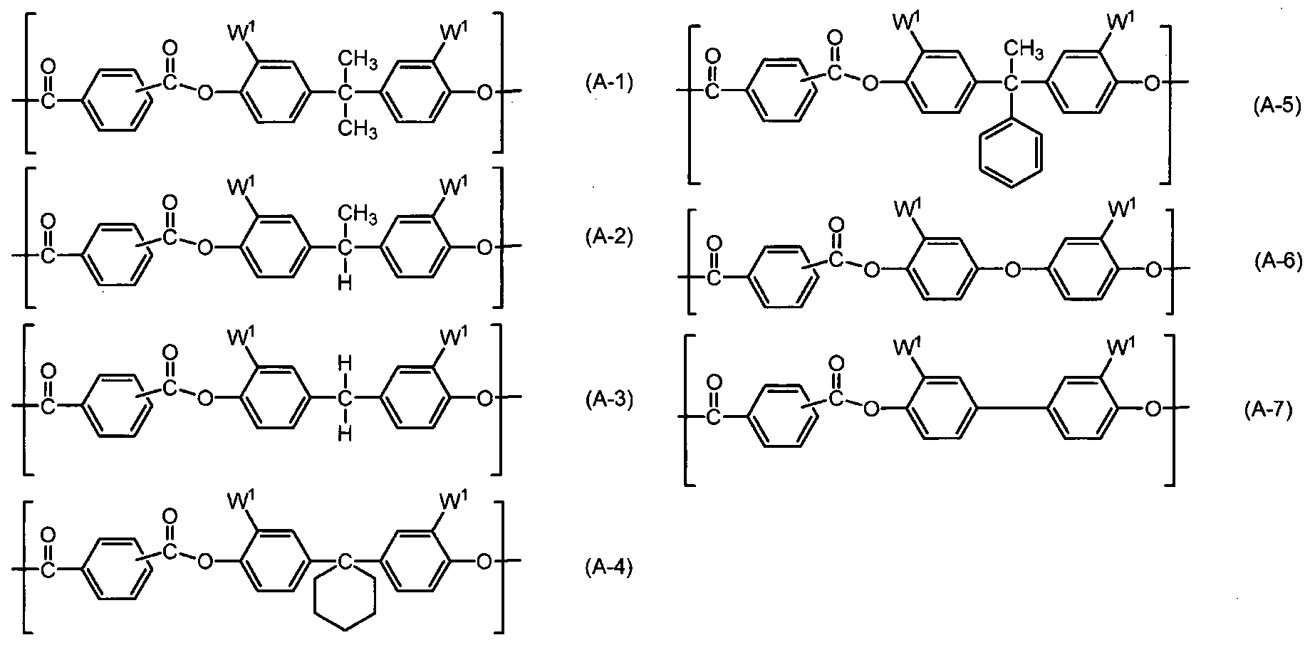
- polyester resin A having a repeating
- Y 1 represents a single bond, a methylene group, an ethylidene group, a propylidene group, a phenylethylidene group, a cyclohexylidene group, or an oxygen atom;
- X 1 represents a meta-phenylene group, a para-phenylene group, or a bivalent group having two para-phenylene groups bonded with an oxygen atom;
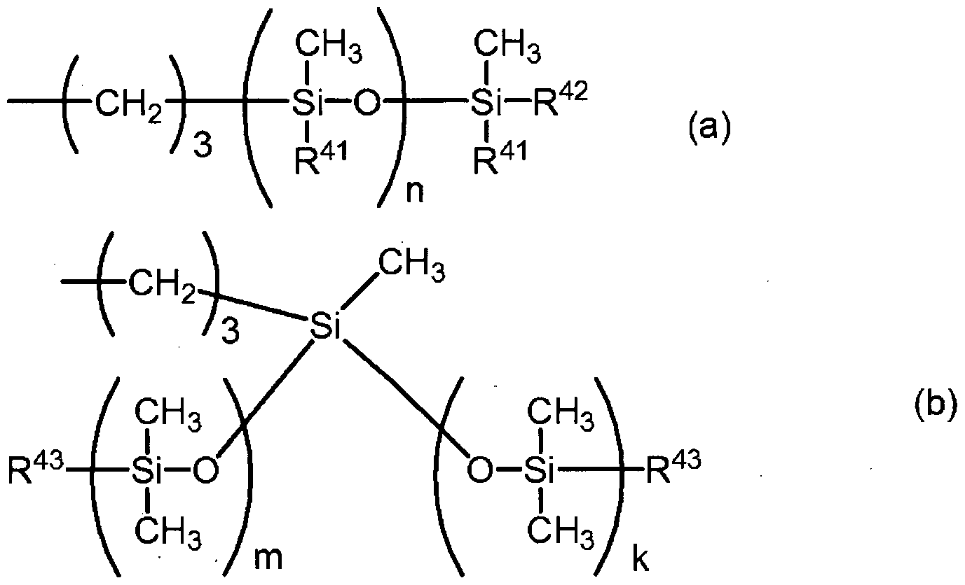
- W 1 represents an univalent group represented by the following formula (a) , or an univalent group represented by the following formula (b) .
- R 41 represents a methyl group or a phenyl group
- R 42 and R 43 each independently represents an alkyl group having 1 to 4 carbon atoms
- "n” represents the number of repetitions of a structure within brackets
- an average of "n” in the polyester resin A ranges from 10 to 150
- "m” and "k” each
- an average of "m+k" in the pol ester resin A ranges from 10 to 150.
- R 51 to R 54 each independently
- X 2 represents a meta-phenylene group, a para-phenylene group, or a bivalent group having two para-phenylene groups bonded with an oxygen atom
- Y 2 represents a single bond, a methylene group, an ethylidene group, a propylidene group, a phenylethylidene group, a
- R bl to R b4 each independently
- Y 3 represents a single bond, a methylene group, an ethylidene group, a propylidene group, a
- phenylethylidene group a cyclohexylidene group, or an oxygen atom.
- R 71 to R 74 each independently
- X 4 represents a meta-phenylene group, a para-phenylene group, and a bivalent group having two para-phenylene groups bonded with an oxygen atom
- Y 4 represents a single bond, a methylene group, an ethylidene group, a propylidene group, a cyclohexylidene group, or an oxygen atom.
- Ar 1 represents a phenyl group, or a phenyl group substituted with a methyl group or an ethyl group
- Ar 21 , Ar 22 , Ar 24 , Ar 25 , Ar 27 , and Ar 28 each independently represents a phenyl group or a tolyl group
- Ar 23 and Ar 26 each independently represents a phenyl group or a tolyl group
- he present invention also relates to a process
- the process cartridge detachably attachable to a main body of an electrophotographic apparatus, wherein the process cartridge integrally supports: the electrophotographic photosensitive member; and at least one device selected from the group consisting of a charging device, a developing device, a transferring device, and a
- the present invention also relates to an
- electrophotographic apparatus comprising: the
- electrophotographic photosensitive member a charging device; an exposing device; a developing device; and a transferring device.
- the present invention also relates to a method of
- the method comprises a step of forming the charge-transporting layer by applying a charge- transporting-layer coating solution on the charge- generating layer and drying the coating solution, and wherein the charge-transporting-layer coating solution comprises: the polyester resin A, at least one resin selected from the group consisting of the polycarbonate resin C and the polyester resin D, and at least one charge-transporting substance selected from the group consisting of the compound represented by the formula (1), the compound represented by the formula ( ⁇ '), the compound represented by the formula (2), and the compound represented by the formula (2').
- the electrophotographic photosensitive member containing a specific charge-transporting substance which has an excellent balance between sustained reduction of contact stress with a contact member or the like and potential stability in repeated use.
- electrophotographic photosensitive member Further, according to the present invention, it is also possible to provide the method of manufacturing the
- FIGURE is a diagram that schematically shows the construction of an electrophotographic apparatus including a process cartridge having an
- a polyester resin A is referred to as
- component ⁇ represented by the formula (2') is referred to as component ⁇ .
- a conductive support includes: a conductive support, a charge-generating layer which is provided on the conductive support and comprises a charge-generating substance, and a charge- transporting layer which is provided on the charge- generating layer and is a surface layer of the
- the charge-transporting layer has a matrix-domain structure having: a matrix which includes a component ⁇ and a component ⁇ ; and a domain which includes a component a.
- the domain including the component a has a granular (island-like) structure formed in the matrix including the components ⁇ and ⁇ .
- the domain including the component a is present in the matrix as an independent domain. Such matrix-domain structure can be confirmed by observing the surface of the charge-transporting layer or the cross-sectional surface of the charge-transporting layer.
- the component a in the present invention is preferably not less than 100 ran and not more than 1,000 nm. Further, the particle size distribution of the particle sizes of each domain is preferably narrow from the viewpoint of sustained effect of reducing contact stress.
- the matrix-domain structure of the charge-transporting layer in the electrophotographic photosensitive member of the present invention can be formed by using a charge-transporting-layer coating solution which
- present invention can be manufactured by applying the charge-transporting-layer coating solution on the charge-generating layer, and drying the coating
- the matrix-domain structure of the present invention is a structure in which the domain including the component a is formed in the matrix including the components ⁇ and ⁇ . It is considered that the effect of reducing contact stress is sustainably exerted by forming the domain including the component a not only on the surface of the charge-transporting layer but also in the charge-transporting layer. Specifically, this is probably because the siloxane resin component having an effect of reducing contact stress, which is reduced by a friction of a member such as paper or a cleaning blade, can be supplied from the domain in the charge- transporting layer.
- the inventors of the present invention have found that, in the case where a charge-transporting substance having a specific structure is used as the charge- transporting substance, the potential stability in repeated use may further be improved. Further, the inventors have estimated the reason of further
- the charge-transporting layer having the matrix-domain structure of the present invention it is important to reduce the charge-transporting substance content in the domain of the formed matrix-domain structure as much as possible for suppressing a
- the component Y in the present invention is a charge-transporting substance having high compatibility with the resin in the charge-transporting layer, and aggregates of the component ⁇ may be easy to form because the component ⁇ is contained in a large amount in the domain including the siloxane-containing resin.
- electrophotographic photosensitive member including the component ⁇ . This is probably because the content of the component ⁇ in the domain is reduced by forming the domain including the component a. This is probably because a branched siloxane structure in the polyester resin A which is the component a can suppress remaining of the component ⁇ having a structure compatible with the resin in the domain.
- the component ⁇ of the present invention is at least one charge-transporting substance selected from the group consisting of a compound represented by the following formula (1), a compound represented by the following formula (l 1 ) , a compound represented by the following formula (2), and a compound represented by the following formula (2 1 ).
- Ar 1 represents a phenyl group or a phenyl group substituted with a methyl group or an ethyl group.
- R 1 represents a phenyl group, a phenyl group
- R 2 represents a hydrogen atom, a phenyl group, or a phenyl group substituted with a methyl group.
- Ar , Ar zz , Ar ⁇ , Ar , Ar , and Ar 28 each independently represents a phenyl group or a tolyl group
- Ar 23 and Ar 26 each independently represents a phenyl group or a tolyl group
- the component ⁇ is preferably a charge- transporting substance having the structure represented by the above-mentioned formula (1-2), (1-3), (1-4), (1- 5), (1-7), (1-8), (1-9), (2-1), or (2-5).
- the component a of the present invention is a polyester resin A having a repeating structural unit represented by the following formula (A) and a repeating structural unit represented by the following formula (B) .
- the content of a siloxane moiety in the polyester resin A is not less than 5.0% by mass (5% by mass) and not more than 40% by mass.
- Y 1 represents a single bond, a methylene group, an ethylidene group, a propylidene group, a phenylethylidene group, a cyclohexylidene group, or an oxygen atom;
- X 1 represents a meta-phenylene group, a para-phenylene group, or a bivalent group having two para-phenylene groups bonded with an oxygen atom;
- W 1 represents an univalent group represented by the following formula (a) , or an univalent group re resented by the following formula (b) .
- R 41 represents a methyl group or a phenyl group
- R 42 and R 43 each independently represents an alkyl group having 1 to 4 carbon atoms
- "n” represents the number of repetitions of a structure within brackets, an average of "n” in the polyester resin A ranges from 10 to 150
- "m” and "k” each
- an average of "m+k" in the polyester resin A ranges from 10 to 150.
- R 51 to R 54 each independently
- X 2 represents a meta-phenylene group, a para-phenylene group, or a bivalent group having two para-phenylene groups bonded with an oxygen atom
- Y 2 represents single bond, a methylene group, an ethylidene group, propylidene group, a phenylethylidene group, a cyclohexylidene group, or an oxygen atom.
- polyester resin A which is the
- the repeating structural unit represented by the above-mentioned formula (A) is preferably a
- an average of "n” in the polyester resin A is 10 or more to 150 or less.
- the average of "n” is preferably 30 or more to 100 or less.
- an average of "m+k” in the polyester resin A is 10 or more to 150 or less.
- the average of "m+k” is preferably 30 or more to 100 or less.
- repetitions of the structures within the brackets fall within the range of +10% of the value represented as the average of the numbers of repetitions of "m+k" because the effect of the present invention can be obtained stably.
- the polyester resin A which is the above- mentioned component a of the present invention contains a siloxane moiety at a content of not less than 5.0% by mass and not more than 40% by mass relative to the total mass of the polyester resin A. If the content of the siloxane moiety is less than 5.0% by mass (5% by mass), a sustained effect of reducing contact stress is insufficient, and a domain is not formed effectively in the matrix containing the component ⁇ or ⁇ . Meanwhile, if the content of the siloxane moiety is more than 40% by mass, the component ⁇ forms aggregates in the domain including the component a, . resulting in insufficient potential stability in repeated use.
- the siloxane moiety is a
- the siloxane moiety which includes silicon atoms present at the both ends of the siloxane structure, groups bonded to the silicon atoms, and oxygen atoms, silicon atoms, and groups bonded to the atoms present between the silicon atoms present at the both ends.
- the siloxane moiety refers to the moiety surrounded by the dashed line in the repeating
- siloxane moiety in the above-mentioned formula (A-S) is also shown below.
- total mass of the polyester resin A which is the component a of the present invention can be analyzed by a general analysis technology.
- An example of the analysis technology is shown below.
- the fractionated polyester resin A which is the component a is hydrolyzed in . the presence of an alkali to decompose the component into a carboxylic acid moiety and a bisphenol moiety.
- Nuclear magnetic resonance spectrum analysis or mass spectrometry is performed for the resultant bisphenol moiety to calculate the number of repetitions of the siloxane moiety and a molar ratio, which are converted into a content (mass ratio) .
- the mass ratio of the siloxane moiety in the polyester resin A which is the component a relates to the amount of a raw material of a monomer unit
- the polyester resin A which is used as the above- mentioned component a in the present invention is the repeating structural unit represented by the above- mentioned formula (A) -the repeating structural unit represented by the above-mentioned formula (B)
- copolymerization may be any form such as block copolymerization, random copolymerization, or alternating copolymerization.
- the weight-average molecular weight of the polyester resin A which is used as the above-mentioned component a in the present invention is preferably not less than 30,000 and not more than 150,000, more preferably not less than 40,000 and not more than
- the weight-average molecular weight of the resin is a weight-average molecular weight in terms of polystyrene measured according to a conventional method by a method described in Japanese Patent Application Laid-Open No. 2007-79555.
- polyester resin A which is the above-mentioned
- component a in the present invention can be synthesized by, for example, a conventional phosgene method or transesterification method.
- the layer of the electrophotographic photosensitive member of the present invention may contain a resin having a siloxane structure in addition to the polyester resin A.
- a resin having a siloxane structure in addition to the polyester resin A.
- Specific examples thereof include a polycarbonate resin having a siloxane structure, a polyester resin having a siloxane structure, and an acrylic resin having a siloxane structure.
- the content of the component a in the charge-transporting layer is preferably not less than 90% by mass and less than 100% by mass relative to the total mass of resins each having a siloxane moiety in the charge-transporting layer .
- resin A of the present invention is preferably not less than 1% by mass and not more than 20% by mass relative to the total mass of whole resins in the charge- transporting layer. If the content of the siloxane moiety is not less than 1% by mass and not more than 20% by mass, the matrix-domain structure is formed stably, resulting in achieving the balance between sustained reduction of contact stress and potential stability in repeated use at high levels. Further, the content is more preferably not less than 2% by mass and not more than 10% by mass, which can further enhance the sustained reduction of contact stress and potential stability in repeated use.
- polyester resin A used as the component a in the present invention is shown below.
- the polyester resin A can be synthesized by synthesis methods described in Japanese Patent Application Laid- Open No. H05-043670 and Japanese Patent Application Laid-Open No. H08-234468. Also in the present
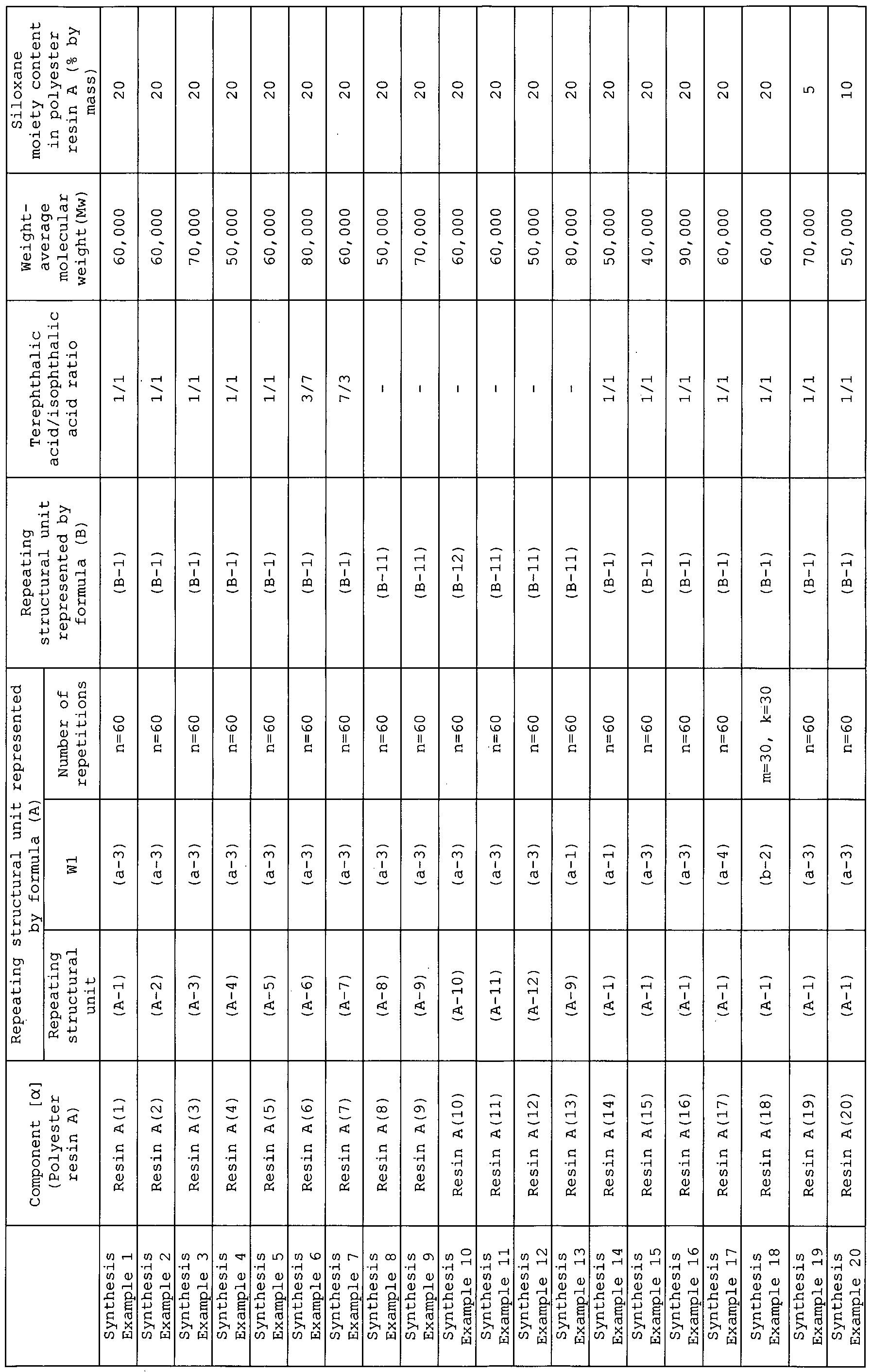
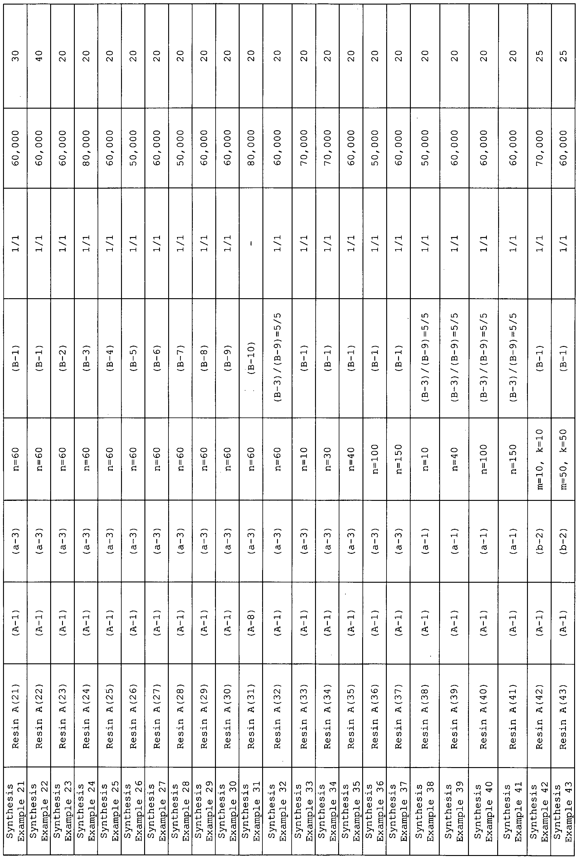
- polyester resins A shown in synthesis examples of Table 1 were synthesized using raw
- Table 1 shows the weight- average molecular weights of the synthesized polyester resins A and the siloxane moiety contents in the polyester resins A. Further, Table 1 shows Comparative Synthesis Example 1 (Resin E(l)) of a polyester resin A having a siloxane moiety content of 2% by mass and Comparative Synthesis Example2 (Resin E(2)) of a polyester resin A having a siloxane moiety content of 50% by mass.
- Tephthalic acid/isophthalic acid ratio refers to ratios of a terephthalic acid
- brackets represented by the above- mentioned formula (b) were 64 and 56, respectively.
- the component ⁇ of the present invention is at least one resin selected from the group consisting of a polycarbonate resin C having a repeating structural unit represented by the following formula (C) and a polyester resin D having a repeating structural unit represented by the following formula (D) .
- R bl to R b4 each independently
- Y 3 represents a single bond, a methylene group, an
- phenylethylidene group a cyclohexylidene group, or an oxygen atom.
- R' 1 to R each independently
- X 4 represents a meta-phenylene group, a para-phenylene group, or a bivalent group having two para-phenylene groups bonded with an oxygen atom.
- Y 4 represents a single bond, a methylene group, an ethylidene group, a propylidene group, a cyclohexylidene group, or an oxygen atom.
- the layer of the electrophotographic photosensitive member of the present invention contains the components a and ⁇ as resins, and an additional resin may be mixed therein.
- the additional resin which may be mixed include an acrylic resin, a polyester resin, and a polycarbonate resin.
- the ratio of the component ⁇ (polycarbonate resin C or polyester resin D) to the additional resin is preferably in a range in which the content of the component ⁇ is not less than 90% by mass and less than 100% by mass (mass ratio) .
- the additional resin in the case where the additional resin is mixed in addition to the component ⁇ , from the viewpoint of forming a uniform matrix with the charge- transporting substance, the additional resin preferably has no siloxane structure.
- the layer of the electrophotographic photosensitive member of the present invention contains the component ⁇ as the charge-transporting substance, and may contain a charge-transporting substance having another structure.
- the charge-transporting substance having another structure include a triarylamine compound and a hydrazone compound. Of those, use of the triarylamine compound as the charge-transporting substance is preferred in terms of potential stability in repeated use.
- the component ⁇ is contained at a content of preferably 50% by mass or more, more preferably 70% by mass or more in whole charge-transporting substances in the charge- transporting layer.
- the electrophotographic photosensitive member of the present invention has a conductive support, a charge- generating layer which is provided on the conductive support and comprises a charge-generating substance, and a charge-transporting layer which is provided on the charge-generating layer, comprises a charge- transporting substance. Further, in the
- the charge- transporting layer is a surface layer (outermost layer) of the electrophotographic photosensitive member.
- electrophotographic photosensitive member of the present invention includes the above-mentioned
- the charge-transporting layer may have a
- the . layer is formed so that at least the charge-transporting layer provided on- the outermost surface has the above- mentioned matrix-domain structure.
- photosensitive layer charge-generating layer or charge-transporting layer
- the member may have a formed of belt or sheet.
- electrophotographic photosensitive member of the present invention is preferably conductive (conductive support) and is, for example, one made of aluminum, an aluminum alloy, or stainless steel.
- the conductive support used may be an ED tube or an EI tube or one obtained by subjecting the ED tube or the EI tube to cutting, electrolytic composite polish, or a wet- or dry-honing process.
- Further examples thereof include a conductive support made of a metal or a resin having formed thereon a thin film of a conductive material such as aluminum, an aluminum alloy, or an indium oxide-tin oxide alloy.
- the surface of the support may be
- conductive particles such as carbon black, tin oxide particles, titanium oxide particles, or silver particles in a resin or the like, or a plastic including a conductive binder resin may be used.
- a conductive layer having conductive particles and a resin may be provided on the support.
- powder containing the conductive particles is contained in the conductive layer.
- the conductive particles include carbon black, acetylene black, metal powders made of, for example, aluminum, nickel, iron, nichrome, copper, zinc, and silver, and metal oxide powders made of, for example, conductive tin oxide and ITO.
- a polyester resin examples include a polyester resin, a polycarbonate resin, a polyvinyl butyral resin, an acrylic resin, a silicone resin, an epoxy resin, a melamine resin, a urethane resin, a phenol resin, and an alkyd resin.
- Those resins may be used each alone or in combination of two or more kinds thereof.
- the film thickness of the conductive layer is preferably 0.2 ⁇ or more to 40 ⁇ or less, more preferably 1 ⁇ or more to 35 ⁇ or less, still more preferably 5 ⁇ or more to 30 ⁇ or [0093] [Intermediate layer]
- the electrophotographic photosensitive member of the present invention may include an intermediate layer between the conductive support or the conductive layer and the charge-generating layer.
- the intermediate layer can be formed by applying an intermediate-layer coating solution containing a resin on the support or the conductive layer and drying or hardening the coating solution.
- Examples of the resin to be used in the intermediate layer include polyacrylic acids, methylcellulose, ethylcellulose, a polyamide resin, a polyimide resin, a polyamideimide resin, a polyamide acid resin, a
- the resin to be used in the intermediate layer is preferably a thermoplastic resin, and specifically, a thermoplastic polyamide resin is preferred.
- a thermoplastic polyamide resin examples include copolymer nylon with low crystallinity or amorphous which can be applied in solution state.
- the intermediate layer may further contain a semiconductive particle, an electron-transporting substance, or an electron-accepting substance.
- the charge-generating layer is provided on the conductive support, conductive layer, or intermediate layer.
- Examples of the charge-generating substance to be used in the electrophotographic photosensitive member of the present invention include azo pigments, phthalocyanine pigments, indigo pigments, and perylene pigments. Only one kind of those charge-generating substances may be used, or two or more kinds thereof may be used. Of those, oxytitanium phthalocyanine, hydroxygallium phthalocyanine, and chlorogallium phthalocyanine are particularly preferred because of their high
- Examples of the resin to be used in the charge- generating layer include a polycarbonate resin, a polyester resin, a butyral resin, a polyvinyl acetal resin, an acrylic resin, a vinyl acetate resin, and a urea resin.
- a butyral resin is particularly preferred.
- One kind of those resins may be used alone, or two or more kinds thereof may be used as a mixture or as a copolymer.
- the charge-generating layer can be formed by applying a charge-generating-layer coating solution, which is prepared by dispersing a charge-generating substance together with a resin and a solvent, and then drying the coating solution. Further, the charge-generating layer may also be a deposited film of a charge- generating substance.
- Examples of the dispersion method include those using a homogenizer, an ultrasonic wave, a ball mill, a sand mill, an attritor, or a roll mill.
- a ratio between the charge-generating substance and the resin is preferably 0.1 part by mass or more to 10 parts by mass or less, particularly preferably 1 part by mass or more to 3 parts by mass or less of the charge-generating substance with respect to 1 part by mass of the resin.
- Examples of the solvent to be used in the charge- generating-layer coating solution include an alcohol- based solvent, a sulfoxide-based solvent, a ketone- based solvent, an ether-based solvent, an ester-based solvent, and an aromatic hydrocarbon solvent.
- he film thickness of the charge-generating layer is preferably 0.01 ⁇ or more to 5 ⁇ or less, more preferably 0.1 ⁇ or more to 2 ⁇ or less.
- the charge-generating layer may be added with any of various sensitizers, antioxidants, UV absorbents, plasticizers, and the like if required.
- a charge- transporting substance or a charge-accepting substance may also be added to the charge-generating layer to prevent the flow of charge from being disrupted in the charge-generating layer.
- the charge-transporting layer is provided on the charge-generating layer.
- the layer of the electrophotographic photosensitive member of the present invention contains the component ⁇ as a specific charge-transporting substance, and may also contain a charge-transporting substance having another structure as described above.
- the charge-transporting substance which has another structure and may be mixed is as described above.
- the layer Of the electrophotographic photosensitive member of the present invention contains the components a and ⁇ as resins, but as described above, another resin may further be mixed.
- the resin which may be mixed is as described above.
- the charge-transporting layer can be formed by applying a charge-transporting-layer coating solution obtained by dissolving a charge-transporting substance and the above-mentioned resins into a solvent and then drying the coating solution.
- a ratio between the charge-transporting substance and the resins is preferably 0.4 part by mass or more to 2 parts by mass or less, more preferably 0.5 part by mass or more to 1.2 parts by mass or less of the charge- transporting substance with respect to 1 part by mass of the resins.
- Examples of the solvent to be used for the charge- transporting-layer coating solution include ketone- based solvents, ester-based solvents, ether-based solvents, and aromatic hydrocarbon solvents. Those solvents may be used each alone or as a mixture of two or more kinds thereof. Of those solvents, it is
- any of the ether-based solvents and the aromatic hydrocarbon solvents from the viewpoint of resin solubility.
- he charge-transporting layer has a film thickness of preferably 5 ⁇ or more to 50 ⁇ or less, more
- the charge-transporting layer may be added with an antioxidant, a UV absorber, or a plasticizer if
- the electrophotographic photosensitive member of the present invention examples include: a deterioration-preventing agent such as an antioxidant, a UV absorber, or a light stabilizer; and fine
- deterioration-preventing agent examples include a hindered phenol-based
- organic fine particles include polymer resin particles such as fluorine atom-containing resin particles, polystyrene fine particles, and polyethylene resin particles.
- examples of the inorganic fine particles include metal oxides such as silica and alumina.
- any of the application methods can be employed, such as dip coating, spraying coating, spinner coating, roller coating, Mayer bar coating, and blade coating.
- FIGURE illustrates an example of the schematic
- photosensitive member 1 can be driven to rotate around an axis 2 in the direction indicated by the arrow at a predetermined peripheral speed.
- the surface of the rotated electrophotographic photosensitive member 1 is uniformly charged in negative at predetermined
- a charging device primary charging device: such as a charging roller
- electrophotographic photosensitive member 1 receives exposure light (image exposure light) 4 which is emitted from an exposing device (not shown) such as a slit exposure or a. laser-beam scanning exposure and which is intensity-modulated according to a time-series electric digital image signal of image information of purpose. In this way, electrostatic latent images corresponding to the image information of purpose are sequentially formed on the surface of the exposing device (not shown) such as a slit exposure or a. laser-beam scanning exposure and which is intensity-modulated according to a time-series electric digital image signal of image information of purpose. In this way, electrostatic latent images corresponding to the image information of purpose are sequentially formed on the surface of the
- he electrostatic latent images formed on the surface of the electrophotographic photosensitive member 1 are converted into toner images by reversal development with toner included in a developer of a developing device 5. Subsequently, the toner images being formed and held on the surface of the electrophotographic photosensitive member 1 are sequentially transferred to a transfer material (such as paper) P. by a transfer bias from a transferring device (such as transfer roller) 6. It should be noted that the transfer material P is taken from a transfer material supplying device (not shown) in synchronization with the rotation of the electrophotographic photosensitive member 1 and fed to a portion (contact part) between the
- bias voltage having a polarity reverse to that of the electric charges the toner has is applied to the transferring device 6 from a bias power source (not shown) .
- he transfer material P which has received the transfer of the toner images is dissociated from the surface of the electrophotographic photosensitive member 1 and then introduced to a fixing device 8.
- the transfer material P is subjected to an image fixation of the toner images and then printed as an image-formed product (print or copy) out of the apparatus.
- the surface of the electrophotographic photosensitive member 1 is subjected to a neutralization process with pre-exposure light (not shown) from a pre-exposing device (not shown) and then repeatedly used in image formation.
- the charging device 3 is a contact-charging device using a charging roller, the pre-exposure is not always
- the process cartridge may be designed so as to be detachably mounted on the main body of an electrophotographic apparatus such as a copying machine or a laser beam printer.
- an electrophotographic apparatus such as a copying machine or a laser beam printer.
- the photosensitive member 1, the charging device 3, the developing device 5, and the cleaning device 7 are integrally supported and placed in a cartridge, thereby forming a process cartridge 9.
- the process cartridge 9 is detachably mounted on the main body of the
- electrophotographic apparatus using a guiding device 10 such as a rail of the main body of the
- the charge-transporting-layer coating solution was applied on the above-mentioned charge- generating layer by dip coating and dried at 110°C for 1 hour, to thereby form a charge-transporting layer with a film thickness of 16 ⁇ . It was confirmed that the resultant charge-transporting layer contained a domain including the component a in a matrix including the components ⁇ and ⁇ .
- Table 2 shows the components , ⁇ , and Y in the resultant charge-transporting layer, the content of the siloxane moiety in the polyester resin A (siloxane content A) , and the content of the siloxane moiety in the polyester resin A relative to the total mass of whole resins in the charge-transporting layer (siloxane content B) .
- electrophotographic photosensitive member was used as an evaluation apparatus. Further, a cleaning blade made of polyurethane rubber was set so as to have a contact angle of 25° and a contact pressure of 35 g/cm 2 relative to the surface of the electrophotographic photosensitive member. Evaluation was performed under an environment of a temperature of 23°C and a relative humidity of 50%.
- the exposure amount (image exposure amount) of a 780-nm laser light source used as an evaluation apparatus was set so that the light intensity on the surface of the electrophotographic photosensitive member was 0.3
- Measurement of the potentials (dark section potential and bright section potential) of the surface of the electrophotographic photosensitive member was performed at a position of a developing device after replacing the developing device by a fixture fixed so that a probe for potential measurement was located at a position of 130 mm from the end of the
- electrophotographic photosensitive member was set to - 450 V, .laser light was irradiated, and the bright section potential obtained by light attenuation from the dark section potential was measured. Further, A4- size plain paper was used to continuously output 2,000 images, and variations of the bright section potentials before and after the output were evaluated. A test chart having a printing ratio of 5% was used. The results are shown in the column "Potential variation" in Table 7.
- a driving current (current A) of a rotary motor of the electrophotographic photosensitive member was measured under the same conditions as those in the evaluation of the potential variation described above.
- an electrophotographic photosensitive member for comparison of a torque relative value was produced by the following method.
- the electrophotographic photosensitive member was prepared in the same manner as in Example 1 except that the polyester resin A(l) which is the component a used in the charge- transporting layer of the electrophotographic
- Example 1 was replaced by the component ⁇ in Table 2, and only the component ⁇ was used as the resin.
- the resultant electrophotographic photosensitive member was used as the
- the resultant electrophotographic photosensitive member for comparison was used to measure a driving current (current B) of a rotary motor of the
- the torque relative value represents a degree of reduction in the contact stress between the
- the cross-sectional surface of the charge-transporting layer obtained by cutting the charge-transporting layer in a vertical direction with respect to the electrophotographic photosensitive member produced by the above-mentioned method, was observed using an ultradeep profile measurement microscope VK-9500
- Electrophotographic photosensitive members were
- Example 1 produced in the same manner as in Example 1 except that the components ⁇ , ⁇ , and ⁇ in the charge-transporting layers were replaced as shown in Tables 2 to 4, and evaluated. It was confirmed that each of the resultant charge-transporting layers contains a domain including the component a in a matrix including the components ⁇ and [ ⁇ ] . Tables 7 and 8 show the results.
- Electrophotographic photosensitive members were
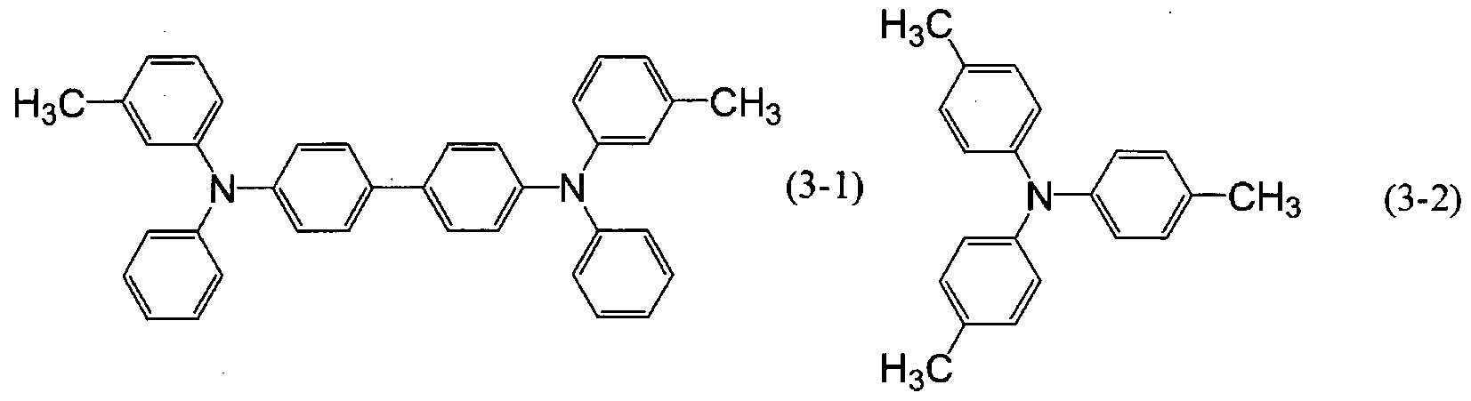
- Example 8 shows the results. It should be noted that a charge-transporting substance having the structure represented by one of the following formulae (3-1) and (3-2) was mixed as the charge-transporting substance with a charge-transporting substance which is the component ⁇ and has the structure represented by one of the above-mentioned formulae (1) and (l 1 ).
- the weight-average molecular weight of the polycarbonate resin C used as the component ⁇ was found to be as follows.
- Electrophotographic photosensitive members were
- Example 8 shows the results.
- the weight-average molecular weight of the polyester resin D used as the component ⁇ were found to be as follows.
- the repeating structural units represented by the above-mentioned formulae (D-l), (D-2), (D-3), (D-4), (D-5) , (D-6), and (D-7) each have a terephthalic acid skeleton/isophthalic acid skeleton ratio of 1/1. ⁇
- Example 1 the electrophotographic photosensitive member for comparison used in Example 1 was used as an
- Electrophotographic photosensitive members were
- Example 1 prepared in the same manner as in Example 1 except that the polyester resin A(l) was replaced by a polyester resin E(2) of Comparative Synthesis Example 2 shown in Table 1, and modifications were made as shown in Table 6. Evaluation was performed in the same manner as in Example 1, and Table 9 shows the results.
- the polyester resin A(l) was replaced by a polyester resin E(2) of Comparative Synthesis Example 2 shown in Table 1, and modifications were made as shown in Table 6. Evaluation was performed in the same manner as in Example 1, and Table 9 shows the results.
- resultant charge-transporting layers were each found to have a matrix-domain structure.
- Electrophotographic photosensitive members were Electrophotographic photosensitive members were Electrophotographic photosensitive members were Electrophotographic photosensitive members were Electrophotographic photosensitive members were
- Example 3 prepared in the same manner as in Example 1 except that, in Example 1, the polyester resin A(l) were replaced to a polyester resin (E(3): weight-average molecular weight: 60,000) containing a repeating structural unit represented by the following formula (E-3) which is a structure described in Patent Literature 1 and a
- An electrophotographic photosensitive member was prepared in the same manner as in Example 63 except that, Example 63, the polyester resin A(2) was replaced to a polycarbonate resin (E(4): weight-average
- Electrophotographic photosensitive members were
- Example 114 produced in the same manner as in Example 114 except that the polyester resin A(l) was replaced by the above-mentioned polycarbonate resin E(4), and
- Electrophotographic photosensitive members were
- Example 6 prepared in the same manner as in Example 1 except that the polyester resin A(l) was replaced by the above- mentioned resin E(3), the charge-transporting substance was replaced by the substance represented by the above- mentioned formula (3-1), and modifications were made as shown in Table 6. Evaluation was performed in the same manner as in Example 1, and Table 9 shows the results. The resultant charge-transporting layers were each found to have a matrix-domain structure. It should be noted that the electrophotographic photosensitive member for comparison used in Example 188 was used as an electrophotographic photosensitive member for comparison of a torque relative value. ⁇
- Electrophotographic photosensitive members were
- Example 6 prepared in the same manner as in Example 1 except that the polyester resin A(l) was replaced by the polyester resin A(21), the charge-transporting substance was replaced by the substance represented by the above- mentioned formula (3-1), and modifications were made as shown in Table 6. Evaluation was performed in the same manner as in Example 1, and Table 9 shows the results. The resultant charge-transporting layers were each found to have a matrix-domain structure. It should be noted that the electrophotographic photosensitive member for comparison used in Example 144 was used as an electrophotographic photosensitive member for
- Component [ ⁇ ] in Tables 2 to 6 refers to the above-mentioned component ⁇ in the charge-transporting layer. In the case of using a mixture of charge- transporting substances, the term refers to the types and mixing ratio of the component ⁇ and another charge- transporting substance.
- Component [a] in Tables 2 to 6 refers to the composition of the above- mentioned component a.
- Siloxane content A (% by mass) in Tables 2 to 6 refers to the content (% by mass) of the siloxane moiety in the polyester resin A.
- Component [ ⁇ ] in Tables 2 to 6 refers to the composition of the above-mentioned component ⁇ .
- the term "Mixing ratio of component [a] to component [ ⁇ ]” in Tables 2 to 6 refers to the mixing ratio (component a/component ⁇ ) of the above-mentioned component a to the above-mentioned component ⁇ in the charge- transporting layer.
- the term "Siloxane content B (% by mass)” in Tables 2 to 6 refers to the content (% by mass) of the siloxane moiety in the polyester resin A relative to the total mass of resins in the charge- transporting layer.
- Resin A(l) 20 4/6 8 88 (1-11) 5) 5/5
- Table 6 refers to the mixing ratio (resin E or resin A/component ⁇ ) of the polycarbonate resin E or the resin A to the above-mentioned component ⁇ in the charge-transporting layer.
- Siloxane content B (% by mass) refers to the content (% by mass) of the siloxane moiety in the "Resin E” relative to the total mass of whole resins in the charge- transporting layer.
- Tables 7 to 9 below show the results of evaluation in Examples 1 to 194 and Comparative Examples 1 to 46.
- Example 7 5 0.65 0.69 460
- Example 8 5 0.65 0.69 460
Landscapes
- Physics & Mathematics (AREA)
- General Physics & Mathematics (AREA)
- Spectroscopy & Molecular Physics (AREA)
- Chemical & Material Sciences (AREA)
- Chemical Kinetics & Catalysis (AREA)
- Photoreceptors In Electrophotography (AREA)
Abstract
Description









Claims


Priority Applications (4)
| Application Number | Priority Date | Filing Date | Title |
|---|---|---|---|
| KR1020137016356A KR101490644B1 (en) | 2010-12-02 | 2011-11-25 | Electrophotographic photosensitive member, process cartridge, electrophotographic apparatus, and method of manufacturing electrophotographic photosensitive member |
| EP11845407.3A EP2646877B1 (en) | 2010-12-02 | 2011-11-25 | Electrophotographic photosensitive member, process cartridge, electrophotographic apparatus, and method of manufacturing electrophotographic photosensitive member |
| CN201180057775.7A CN103238114B (en) | 2010-12-02 | 2011-11-25 | The method of electrophotographic photosensitive element, handle box, electronic photographing device and manufacture electrophotographic photosensitive element |
| US13/988,731 US8980509B2 (en) | 2010-12-02 | 2011-11-25 | Electrophotographic photosensitive member, process cartridge, electrophotographic apparatus, and method of manufacturing electrophotographic photosensitive member |
Applications Claiming Priority (2)
| Application Number | Priority Date | Filing Date | Title |
|---|---|---|---|
| JP2010269732 | 2010-12-02 | ||
| JP2010-269732 | 2010-12-02 |
Publications (1)
| Publication Number | Publication Date |
|---|---|
| WO2012074082A1 true WO2012074082A1 (en) | 2012-06-07 |
Family
ID=46172004
Family Applications (1)
| Application Number | Title | Priority Date | Filing Date |
|---|---|---|---|
| PCT/JP2011/077885 Ceased WO2012074082A1 (en) | 2010-12-02 | 2011-11-25 | Electrophotographic photosensitive member, process cartridge, electrophotographic apparatus, and method of manufacturing electrophotographic photosensitive member |
Country Status (6)
| Country | Link |
|---|---|
| US (1) | US8980509B2 (en) |
| EP (1) | EP2646877B1 (en) |
| JP (1) | JP4959024B1 (en) |
| KR (1) | KR101490644B1 (en) |
| CN (1) | CN103238114B (en) |
| WO (1) | WO2012074082A1 (en) |
Cited By (3)
| Publication number | Priority date | Publication date | Assignee | Title |
|---|---|---|---|---|
| EP2713208A1 (en) * | 2012-09-28 | 2014-04-02 | Canon Kabushiki Kaisha | Electrophotographic photosensitive member, process cartridge and electrophotographic apparatus |
| CN103809397A (en) * | 2012-11-14 | 2014-05-21 | 佳能株式会社 | Electrophotographic photosensitive member, process cartridge, and electrophotographic apparatus |
| EP2757420A1 (en) * | 2013-01-18 | 2014-07-23 | Canon Kabushiki Kaisha | Electrophotographic photosensitive member, process cartridge and electrophotographic apparatus |
Families Citing this family (39)
| Publication number | Priority date | Publication date | Assignee | Title |
|---|---|---|---|---|
| JP4959022B2 (en) | 2010-10-29 | 2012-06-20 | キヤノン株式会社 | Electrophotographic photosensitive member, process cartridge, and electrophotographic apparatus |
| JP5036901B1 (en) | 2010-10-29 | 2012-09-26 | キヤノン株式会社 | Electrophotographic photosensitive member, process cartridge, electrophotographic apparatus, and method of manufacturing electrophotographic photosensitive member |
| JP4975185B1 (en) | 2010-11-26 | 2012-07-11 | キヤノン株式会社 | Method for forming uneven shape on surface of surface layer of cylindrical electrophotographic photoreceptor, and method for producing cylindrical electrophotographic photoreceptor having uneven surface formed on surface of surface layer |
| JP5079153B1 (en) | 2011-03-03 | 2012-11-21 | キヤノン株式会社 | Electrophotographic photosensitive member, process cartridge and electrophotographic apparatus, and method for manufacturing electrophotographic photosensitive member |
| JP5054238B1 (en) | 2011-03-03 | 2012-10-24 | キヤノン株式会社 | Method for producing electrophotographic photosensitive member |
| JP5089815B2 (en) | 2011-04-12 | 2012-12-05 | キヤノン株式会社 | Electrophotographic photosensitive member, process cartridge, electrophotographic apparatus, and method of manufacturing electrophotographic photosensitive member |
| JP5089816B2 (en) | 2011-04-12 | 2012-12-05 | キヤノン株式会社 | Electrophotographic photosensitive member, process cartridge, electrophotographic apparatus, and method of manufacturing electrophotographic photosensitive member |
| JP6108842B2 (en) | 2012-06-29 | 2017-04-05 | キヤノン株式会社 | Method for producing electrophotographic photosensitive member |
| US9029054B2 (en) | 2012-06-29 | 2015-05-12 | Canon Kabushiki Kaisha | Electrophotographic photosensitive member, process cartridge, and electrophotographic apparatus |
| CN103529662B (en) | 2012-06-29 | 2016-05-18 | 佳能株式会社 | Electrophotographic photosensitive element, handle box and electronic photographing device |
| CN103529663B (en) | 2012-06-29 | 2016-04-20 | 佳能株式会社 | Electrophotographic photosensitive element, handle box and electronic photographing device |
| JP6168905B2 (en) * | 2012-09-28 | 2017-07-26 | キヤノン株式会社 | Electrophotographic photosensitive member, process cartridge, and electrophotographic apparatus |
| JP6489824B2 (en) * | 2014-01-31 | 2019-03-27 | キヤノン株式会社 | Electrophotographic photosensitive member, process cartridge, and electrophotographic apparatus |
| US9684277B2 (en) | 2014-11-19 | 2017-06-20 | Canon Kabushiki Kaisha | Process cartridge and image-forming method |
| JP6588731B2 (en) | 2015-05-07 | 2019-10-09 | キヤノン株式会社 | Electrophotographic photosensitive member, process cartridge, and electrophotographic apparatus |
| JP6639256B2 (en) | 2016-02-10 | 2020-02-05 | キヤノン株式会社 | Electrophotographic apparatus and process cartridge |
| US10331052B2 (en) * | 2016-12-20 | 2019-06-25 | Canon Kabushiki Kaisha | Electrophotographic photosensitive member, process cartridge, and electrophotographic apparatus |
| US10162278B2 (en) | 2017-02-28 | 2018-12-25 | Canon Kabushiki Kaisha | Electrophotographic photosensitive member, process cartridge and electrophotographic apparatus |
| US10203617B2 (en) | 2017-02-28 | 2019-02-12 | Canon Kabushiki Kaisha | Electrophotographic photosensitive member, process cartridge and electrophotographic apparatus |
| JP6658664B2 (en) * | 2017-04-28 | 2020-03-04 | 京セラドキュメントソリューションズ株式会社 | Electrophotographic photoreceptor, process cartridge and image forming apparatus |
| JP6850205B2 (en) | 2017-06-06 | 2021-03-31 | キヤノン株式会社 | Electrophotographic photosensitive members, process cartridges and electrophotographic equipment |
| JP7046571B2 (en) | 2017-11-24 | 2022-04-04 | キヤノン株式会社 | Process cartridges and electrophotographic equipment |
| JP7057104B2 (en) | 2017-11-24 | 2022-04-19 | キヤノン株式会社 | Process cartridge and electrophotographic image forming apparatus |
| JP7187270B2 (en) | 2017-11-24 | 2022-12-12 | キヤノン株式会社 | Process cartridge and electrophotographic device |
| JP7034769B2 (en) | 2018-02-28 | 2022-03-14 | キヤノン株式会社 | Electrophotographic photosensitive members, process cartridges and electrophotographic equipment |
| JP2019152699A (en) | 2018-02-28 | 2019-09-12 | キヤノン株式会社 | Electrophotographic photoreceptor, process cartridge, and electrophotographic device |
| JP7034768B2 (en) | 2018-02-28 | 2022-03-14 | キヤノン株式会社 | Process cartridge and image forming equipment |
| JP7150485B2 (en) | 2018-05-31 | 2022-10-11 | キヤノン株式会社 | Electrophotographic photoreceptor, process cartridge and electrophotographic apparatus |
| JP7054366B2 (en) | 2018-05-31 | 2022-04-13 | キヤノン株式会社 | Electrophotographic photosensitive members, process cartridges and electrophotographic equipment |
| US10747130B2 (en) | 2018-05-31 | 2020-08-18 | Canon Kabushiki Kaisha | Process cartridge and electrophotographic apparatus |
| JP7059111B2 (en) | 2018-05-31 | 2022-04-25 | キヤノン株式会社 | Electrophotographic photosensitive member and its manufacturing method, as well as process cartridge and electrophotographic image forming apparatus. |
| JP7059112B2 (en) | 2018-05-31 | 2022-04-25 | キヤノン株式会社 | Electrophotographic photosensitive member, process cartridge and electrophotographic image forming apparatus |
| JP7129225B2 (en) | 2018-05-31 | 2022-09-01 | キヤノン株式会社 | Electrophotographic photoreceptor and method for producing electrophotographic photoreceptor |
| JP7413054B2 (en) | 2019-02-14 | 2024-01-15 | キヤノン株式会社 | Electrophotographic photoreceptors, process cartridges, and electrophotographic devices |
| US11573499B2 (en) | 2019-07-25 | 2023-02-07 | Canon Kabushiki Kaisha | Process cartridge and electrophotographic apparatus |
| US11320754B2 (en) | 2019-07-25 | 2022-05-03 | Canon Kabushiki Kaisha | Process cartridge and electrophotographic apparatus |
| JP7337652B2 (en) | 2019-10-18 | 2023-09-04 | キヤノン株式会社 | Process cartridge and electrophotographic apparatus using the same |
| JP7337649B2 (en) | 2019-10-18 | 2023-09-04 | キヤノン株式会社 | Process cartridge and electrophotographic device |
| JP7838985B2 (en) | 2022-03-14 | 2026-04-01 | キヤノン株式会社 | Process cartridges and electrophotographic devices |
Citations (3)
| Publication number | Priority date | Publication date | Assignee | Title |
|---|---|---|---|---|
| JPH08262752A (en) * | 1995-03-28 | 1996-10-11 | Konica Corp | Electrophotographic photoreceptor, electrophotographic device and device unit |
| JP2009180760A (en) * | 2008-01-29 | 2009-08-13 | Mitsubishi Gas Chem Co Inc | Binder resin for the photosensitive layer of electrophotographic photoreceptors. |
| JP4764953B1 (en) * | 2009-12-09 | 2011-09-07 | キヤノン株式会社 | Electrophotographic photosensitive member, process cartridge, and electrophotographic apparatus |
Family Cites Families (37)
| Publication number | Priority date | Publication date | Assignee | Title |
|---|---|---|---|---|
| JPH0543670A (en) | 1991-08-09 | 1993-02-23 | Unitika Ltd | Polyarylate and its production |
| JP3084861B2 (en) | 1991-12-06 | 2000-09-04 | 三菱化学株式会社 | Electrophotographic photoreceptor |
| JPH05155999A (en) * | 1991-12-06 | 1993-06-22 | Mitsubishi Kasei Corp | Polycarbonate resin having polysiloxane in side chain and method for producing the same |
| JPH08234468A (en) | 1995-02-24 | 1996-09-13 | Konica Corp | Electrophotographic photoreceptor |
| JP2002214807A (en) * | 2001-01-17 | 2002-07-31 | Mitsubishi Chemicals Corp | Electrophotographic photoreceptor |
| DE60324219D1 (en) | 2002-04-26 | 2008-12-04 | Canon Kk | Electrophotographic photosensitive member, process cartridge and electrophotographic apparatus |
| JP3913148B2 (en) | 2002-08-30 | 2007-05-09 | キヤノン株式会社 | Electrophotographic photosensitive member, process cartridge, and electrophotographic apparatus |
| JP4174391B2 (en) | 2002-08-30 | 2008-10-29 | キヤノン株式会社 | Electrophotographic photosensitive member, process cartridge, and electrophotographic apparatus |
| US7001699B2 (en) | 2002-08-30 | 2006-02-21 | Canon Kabushiki Kaisha | Electrophotographic photosensitive member, process cartridge and electrophotographic apparatus |
| WO2006028232A1 (en) | 2004-09-10 | 2006-03-16 | Canon Kabushiki Kaisha | Electrophotographic photosensitive member, process cartridge and electrophotographic apparatus |
| JP4679914B2 (en) | 2005-01-27 | 2011-05-11 | キヤノン化成株式会社 | Conductive roller, process cartridge having the conductive roller, and electrophotographic apparatus |
| JP4847245B2 (en) | 2005-08-15 | 2011-12-28 | キヤノン株式会社 | Electrophotographic photosensitive member, process cartridge, and electrophotographic apparatus |
| JP4101279B2 (en) | 2006-01-31 | 2008-06-18 | キヤノン株式会社 | Electrophotographic photosensitive member, process cartridge, and electrophotographic apparatus |
| JP4183267B2 (en) | 2006-01-31 | 2008-11-19 | キヤノン株式会社 | Electrophotographic photosensitive member, process cartridge, and electrophotographic apparatus |
| JP4194631B2 (en) | 2006-01-31 | 2008-12-10 | キヤノン株式会社 | Image forming method and electrophotographic apparatus using the image forming method |
| JP4059518B2 (en) | 2006-01-31 | 2008-03-12 | キヤノン株式会社 | Method for producing electrophotographic photosensitive member |
| JP4101278B2 (en) | 2006-01-31 | 2008-06-18 | キヤノン株式会社 | Electrophotographic photosensitive member, process cartridge, and electrophotographic apparatus |
| KR101189027B1 (en) | 2006-10-31 | 2012-10-08 | 캐논 가부시끼가이샤 | Electrophotographic photosensitive body, method for producing electrophotographic photosensitive body, process cartridge, and electrophotographic device |
| WO2008053906A1 (en) | 2006-10-31 | 2008-05-08 | Canon Kabushiki Kaisha | Electrophotographic photosensitive body, method for producing electrophotographic photosensitive body, process cartridge, and electrophotographic device |
| JP4018741B1 (en) | 2007-01-26 | 2007-12-05 | キヤノン株式会社 | Method for producing a solid having a concave shape on the surface |
| JP4041921B1 (en) | 2007-01-26 | 2008-02-06 | キヤノン株式会社 | Electrophotographic photoreceptor manufacturing method |
| KR101167370B1 (en) | 2007-03-27 | 2012-07-19 | 캐논 가부시끼가이샤 | Electrophotographic photosensitive material, process cartridge and electrophotographic apparatus |
| JP4372213B2 (en) | 2007-03-28 | 2009-11-25 | キヤノン株式会社 | Electrophotographic photosensitive member, process cartridge, and electrophotographic apparatus |
| JP4235673B2 (en) | 2007-07-17 | 2009-03-11 | キヤノン株式会社 | Method for producing electrophotographic photosensitive member |
| EP2306247B1 (en) * | 2008-07-18 | 2016-09-07 | Canon Kabushiki Kaisha | Electrophotographic photoreceptor, process cartridge, and electrophotographic apparatus |
| CN102165375B (en) | 2008-09-26 | 2013-06-19 | 佳能株式会社 | Electrophotographic photosensitive member, process cartridge, and electrophotographic apparatus |
| JP4663819B1 (en) | 2009-08-31 | 2011-04-06 | キヤノン株式会社 | Electrophotographic equipment |
| JP4743921B1 (en) | 2009-09-04 | 2011-08-10 | キヤノン株式会社 | Electrophotographic photosensitive member, process cartridge, and electrophotographic apparatus |
| JP5629588B2 (en) | 2010-01-15 | 2014-11-19 | キヤノン株式会社 | Electrophotographic photosensitive member, process cartridge, and electrophotographic apparatus |
| CN103109236B (en) | 2010-09-14 | 2015-03-25 | 佳能株式会社 | Electrophotographic photosensitive member, process cartridge, electrophotographic apparatus, and method of manufacturing electrophotographic photosensitive member |
| JP4948670B2 (en) | 2010-10-14 | 2012-06-06 | キヤノン株式会社 | Electrophotographic photosensitive member, process cartridge, electrophotographic apparatus, and method of manufacturing electrophotographic photosensitive member |
| JP5036901B1 (en) | 2010-10-29 | 2012-09-26 | キヤノン株式会社 | Electrophotographic photosensitive member, process cartridge, electrophotographic apparatus, and method of manufacturing electrophotographic photosensitive member |
| JP4959022B2 (en) | 2010-10-29 | 2012-06-20 | キヤノン株式会社 | Electrophotographic photosensitive member, process cartridge, and electrophotographic apparatus |
| JP4975185B1 (en) | 2010-11-26 | 2012-07-11 | キヤノン株式会社 | Method for forming uneven shape on surface of surface layer of cylindrical electrophotographic photoreceptor, and method for producing cylindrical electrophotographic photoreceptor having uneven surface formed on surface of surface layer |
| JP5079153B1 (en) | 2011-03-03 | 2012-11-21 | キヤノン株式会社 | Electrophotographic photosensitive member, process cartridge and electrophotographic apparatus, and method for manufacturing electrophotographic photosensitive member |
| JP5054238B1 (en) | 2011-03-03 | 2012-10-24 | キヤノン株式会社 | Method for producing electrophotographic photosensitive member |
| JP5755162B2 (en) | 2011-03-03 | 2015-07-29 | キヤノン株式会社 | Method for producing electrophotographic photosensitive member |
-
2011
- 2011-11-24 JP JP2011256477A patent/JP4959024B1/en active Active
- 2011-11-25 CN CN201180057775.7A patent/CN103238114B/en active Active
- 2011-11-25 US US13/988,731 patent/US8980509B2/en active Active
- 2011-11-25 WO PCT/JP2011/077885 patent/WO2012074082A1/en not_active Ceased
- 2011-11-25 KR KR1020137016356A patent/KR101490644B1/en not_active Expired - Fee Related
- 2011-11-25 EP EP11845407.3A patent/EP2646877B1/en not_active Not-in-force
Patent Citations (3)
| Publication number | Priority date | Publication date | Assignee | Title |
|---|---|---|---|---|
| JPH08262752A (en) * | 1995-03-28 | 1996-10-11 | Konica Corp | Electrophotographic photoreceptor, electrophotographic device and device unit |
| JP2009180760A (en) * | 2008-01-29 | 2009-08-13 | Mitsubishi Gas Chem Co Inc | Binder resin for the photosensitive layer of electrophotographic photoreceptors. |
| JP4764953B1 (en) * | 2009-12-09 | 2011-09-07 | キヤノン株式会社 | Electrophotographic photosensitive member, process cartridge, and electrophotographic apparatus |
Non-Patent Citations (1)
| Title |
|---|
| See also references of EP2646877A4 * |
Cited By (8)
| Publication number | Priority date | Publication date | Assignee | Title |
|---|---|---|---|---|
| EP2713208A1 (en) * | 2012-09-28 | 2014-04-02 | Canon Kabushiki Kaisha | Electrophotographic photosensitive member, process cartridge and electrophotographic apparatus |
| CN103713484A (en) * | 2012-09-28 | 2014-04-09 | 佳能株式会社 | Electrophotographic photosensitive member, process cartridge and electrophotographic apparatus |
| US9235144B2 (en) | 2012-09-28 | 2016-01-12 | Canon Kabushiki Kaisha | Electrophotographic photosensitive member, process cartridge and electrophotographic apparatus |
| CN103809397A (en) * | 2012-11-14 | 2014-05-21 | 佳能株式会社 | Electrophotographic photosensitive member, process cartridge, and electrophotographic apparatus |
| EP2733536A1 (en) * | 2012-11-14 | 2014-05-21 | Canon Kabushiki Kaisha | Electrophotographic photosensitive member, process cartridge, and electrophotographic apparatus |
| US9229342B2 (en) | 2012-11-14 | 2016-01-05 | Canon Kabushiki Kaisha | Electrophotographic photosensitive member, process cartridge, and electrophotographic apparatus |
| EP2757420A1 (en) * | 2013-01-18 | 2014-07-23 | Canon Kabushiki Kaisha | Electrophotographic photosensitive member, process cartridge and electrophotographic apparatus |
| US9164406B2 (en) | 2013-01-18 | 2015-10-20 | Canon Kabushiki Kaisha | Electrophotographic photosensitive member, process cartridge and electrophotographic apparatus |
Also Published As
| Publication number | Publication date |
|---|---|
| EP2646877A1 (en) | 2013-10-09 |
| CN103238114B (en) | 2016-05-11 |
| EP2646877B1 (en) | 2017-03-01 |
| CN103238114A (en) | 2013-08-07 |
| KR20130098415A (en) | 2013-09-04 |
| JP4959024B1 (en) | 2012-06-20 |
| US8980509B2 (en) | 2015-03-17 |
| US20130236823A1 (en) | 2013-09-12 |
| JP2012133341A (en) | 2012-07-12 |
| KR101490644B1 (en) | 2015-02-05 |
| EP2646877A4 (en) | 2016-07-06 |
Similar Documents
| Publication | Publication Date | Title |
|---|---|---|
| EP2646877B1 (en) | Electrophotographic photosensitive member, process cartridge, electrophotographic apparatus, and method of manufacturing electrophotographic photosensitive member | |
| US8753789B2 (en) | Electrophotographic photosensitive member, process cartridge, electrophotographic apparatus, and method of manufacturing electrophotographic photosensitive member | |
| EP2633369B1 (en) | Electrophotographic photosensitive member, process cartridge, electrophotographic apparatus, and method of manufacturing electrophotographic photosensitive member | |
| KR101442443B1 (en) | Electrophotographic photosensitive member, process cartridge, electrophotographic apparatus, and method of manufacturing electrophotographic photosensitive member | |
| KR101488129B1 (en) | Electrophotographic photosensitive member, process cartridge, electrophotographic apparatus and method of manufacturing the electrophotographic photosensitive member | |
| KR101486184B1 (en) | Electrophotographic photosensitive member, process cartridge, electrophotographic apparatus and method of manufacturing the electrophotographic photosensitive member | |
| KR20140070398A (en) | Electrophotographic photosensitive member, method for producing electrophotographic photosensitive member, process cartridge and electrophotographic apparatus | |
| JP5491208B2 (en) | Electrophotographic photosensitive member, process cartridge, and electrophotographic apparatus |
Legal Events
| Date | Code | Title | Description |
|---|---|---|---|
| WWE | Wipo information: entry into national phase |
Ref document number: 201180057775.7 Country of ref document: CN |
|
| 121 | Ep: the epo has been informed by wipo that ep was designated in this application |
Ref document number: 11845407 Country of ref document: EP Kind code of ref document: A1 |
|
| REEP | Request for entry into the european phase |
Ref document number: 2011845407 Country of ref document: EP |
|
| WWE | Wipo information: entry into national phase |
Ref document number: 2011845407 Country of ref document: EP |
|
| WWE | Wipo information: entry into national phase |
Ref document number: 13988731 Country of ref document: US |
|
| NENP | Non-entry into the national phase |
Ref country code: DE |
|
| ENP | Entry into the national phase |
Ref document number: 20137016356 Country of ref document: KR Kind code of ref document: A |