WO2012086623A1 - 発光素子 - Google Patents
発光素子 Download PDFInfo
- Publication number
- WO2012086623A1 WO2012086623A1 PCT/JP2011/079449 JP2011079449W WO2012086623A1 WO 2012086623 A1 WO2012086623 A1 WO 2012086623A1 JP 2011079449 W JP2011079449 W JP 2011079449W WO 2012086623 A1 WO2012086623 A1 WO 2012086623A1
- Authority
- WO
- WIPO (PCT)
- Prior art keywords
- light
- light emitting
- layer
- row
- concavo
- Prior art date
- Legal status (The legal status is an assumption and is not a legal conclusion. Google has not performed a legal analysis and makes no representation as to the accuracy of the status listed.)
- Ceased
Links
Images


Classifications
-
- H—ELECTRICITY
- H10—SEMICONDUCTOR DEVICES; ELECTRIC SOLID-STATE DEVICES NOT OTHERWISE PROVIDED FOR
- H10K—ORGANIC ELECTRIC SOLID-STATE DEVICES
- H10K50/00—Organic light-emitting devices
- H10K50/80—Constructional details
- H10K50/85—Arrangements for extracting light from the devices
- H10K50/854—Arrangements for extracting light from the devices comprising scattering means
-
- H—ELECTRICITY
- H10—SEMICONDUCTOR DEVICES; ELECTRIC SOLID-STATE DEVICES NOT OTHERWISE PROVIDED FOR
- H10K—ORGANIC ELECTRIC SOLID-STATE DEVICES
- H10K50/00—Organic light-emitting devices
- H10K50/80—Constructional details
- H10K50/85—Arrangements for extracting light from the devices
-
- H—ELECTRICITY
- H10—SEMICONDUCTOR DEVICES; ELECTRIC SOLID-STATE DEVICES NOT OTHERWISE PROVIDED FOR
- H10K—ORGANIC ELECTRIC SOLID-STATE DEVICES
- H10K50/00—Organic light-emitting devices
- H10K50/80—Constructional details
- H10K50/85—Arrangements for extracting light from the devices
- H10K50/856—Arrangements for extracting light from the devices comprising reflective means
-
- G—PHYSICS
- G02—OPTICS
- G02B—OPTICAL ELEMENTS, SYSTEMS OR APPARATUS
- G02B5/00—Optical elements other than lenses
- G02B5/02—Diffusing elements; Afocal elements
- G02B5/0205—Diffusing elements; Afocal elements characterised by the diffusing properties
- G02B5/021—Diffusing elements; Afocal elements characterised by the diffusing properties the diffusion taking place at the element's surface, e.g. by means of surface roughening or microprismatic structures
- G02B5/0215—Diffusing elements; Afocal elements characterised by the diffusing properties the diffusion taking place at the element's surface, e.g. by means of surface roughening or microprismatic structures the surface having a regular structure
-
- G—PHYSICS
- G02—OPTICS
- G02B—OPTICAL ELEMENTS, SYSTEMS OR APPARATUS
- G02B5/00—Optical elements other than lenses
- G02B5/02—Diffusing elements; Afocal elements
- G02B5/0205—Diffusing elements; Afocal elements characterised by the diffusing properties
- G02B5/021—Diffusing elements; Afocal elements characterised by the diffusing properties the diffusion taking place at the element's surface, e.g. by means of surface roughening or microprismatic structures
- G02B5/0231—Diffusing elements; Afocal elements characterised by the diffusing properties the diffusion taking place at the element's surface, e.g. by means of surface roughening or microprismatic structures the surface having microprismatic or micropyramidal shape
Definitions
- the present invention relates to a light emitting element. Specifically, the present invention relates to a light-emitting element including an organic electroluminescence element (hereinafter referred to as “organic EL element” as appropriate).
- organic EL element an organic electroluminescence element
- a light-emitting element including an organic EL element can have a planar shape, and the color of the light can be white or a color close thereto. For this reason, it is possible to use a light emitting element provided with an organic EL element for the use as a light source of the lighting fixture which illuminates spaces, such as a living environment, or as a backlight of a display apparatus.
- a problem is that rainbow-like color unevenness (hereinafter referred to as “rainbow unevenness”) is observed when light irradiated from the outside of the element is reflected by the surface of the concavo-convex structure. was there. Such rainbow unevenness deteriorates the quality of the light emitting element as a light source, and is preferably prevented.
- the conventional light emitting element having a concavo-convex structure when the azimuth angle at which the observer views the light emitting element changes, the appearance of the light emitting surface of the light emitting element, such as the color and brightness, also changes. Another problem is that the appearance of the element varies greatly.
- the present invention was devised in view of the above problems, and provides a light-emitting element that has high light extraction efficiency, small rainbow unevenness, and small variation in appearance depending on the azimuth angle at which an observer views the light-emitting element. With the goal.
- the present inventor has provided a concavo-convex structure layer having a concavo-convex structure on the surface opposite to the organic EL element on the light emitting surface of the organic EL element, thereby extracting light by the concavo-convex structure. It has been found that the efficiency can be increased.
- the concavo-convex structure include an concavo-convex structure including three or more groups of rows extending in different directions, the degree of rainbow unevenness can be suppressed, and the observer views the light emitting element. It was found that the change in appearance due to the azimuth can also be suppressed. Based on the above findings, the present invention has been completed. That is, the present invention is as follows [1] to [6].
- An organic electroluminescence device that has a light emitting surface and emits light from the light emitting surface, and a structural layer provided directly or indirectly on the light emitting surface of the organic electroluminescence device,
- the structural layer includes a first row extending in a first direction parallel to the surface on a surface of the structural layer opposite to the organic electroluminescence element, and the first parallel to the surface and the first
- a second row extending in a second direction intersecting with the direction of the second, and a third row extending in a third direction parallel to the surface and intersecting the first direction and the second direction.
- a light-emitting element having an uneven structure including a row.
- the concavo-convex structure is parallel to the surface of the structural layer opposite to the organic electroluminescence element and intersects the first direction, the second direction, and the third direction.
- the uneven structure has a slope inclined with respect to the light emitting surface
- the light emitting device according to any one of [1] to [4], wherein an average inclination angle of the inclined surface with respect to the light emitting surface is 55 ° or more and 85 ° or less.
- the light-emitting element of the present invention has high light extraction efficiency, small rainbow unevenness, and small change in appearance depending on the azimuth angle at which the observer views the light-emitting element.
- FIG. 1 is a perspective view schematically showing a light emitting device according to the first embodiment of the present invention.
- FIG. 2 is a diagram for explaining the light emitting device according to the first embodiment of the present invention, and schematically shows a cross section of the light emitting device shown in FIG. 1 cut along a plane including the lines 1a-1b and perpendicular to the light emitting surface.
- FIG. 3 is an enlarged plan view schematically showing a light output surface of the light emitting device according to the first embodiment of the present invention as viewed from the thickness direction of the light emitting device.
- FIG. 1 is a perspective view schematically showing a light emitting device according to the first embodiment of the present invention.
- FIG. 2 is a diagram for explaining the light emitting device according to the first embodiment of the present invention, and schematically shows a cross section of the light emitting device shown in FIG. 1 cut along a plane including the lines 1a-1b and perpendicular to the light emitting surface.
- FIG. 3 is an enlarged plan view schematic
- FIG. 4 is a plan view schematically showing an enlarged view of the light-emitting surface of the light-emitting element according to the first embodiment of the present invention viewed from the thickness direction of the light-emitting element.
- FIG. 5 is a plan view schematically showing an enlarged view of the light-emitting surface of the light-emitting element according to the first embodiment of the present invention viewed from the thickness direction of the light-emitting element.
- FIG. 6 is a plan view schematically showing an enlarged view of the light-emitting surface of the light-emitting element according to the first embodiment of the present invention viewed from the thickness direction of the light-emitting element.
- FIG. 5 is a plan view schematically showing an enlarged view of the light-emitting surface of the light-emitting element according to the first embodiment of the present invention viewed from the thickness direction of the light-emitting element.
- FIG. 7 is a plan view schematically showing an enlarged view of the light-emitting surface of the light-emitting element according to the first embodiment of the present invention viewed from the thickness direction of the light-emitting element.
- FIG. 8 is a partial cross-sectional view schematically showing a cross section of a part of the concavo-convex structure layer according to the first embodiment of the present invention, taken along a plane that includes the line 3a of FIG. 3 and is perpendicular to the light exit surface.
- FIG. 9 shows a light emitting device according to the second embodiment of the present invention parallel to the point where the third row and the fourth row intersect and the direction in which the first row extends through the recess.
- FIG. 10 is a perspective view schematically showing a light emitting device according to the third embodiment of the present invention.
- FIG. 11 is a plan view schematically showing an enlarged view of the light-emitting surface of the light-emitting element according to the modification of the first embodiment of the present invention when viewed from the thickness direction of the light-emitting element.
- FIG. 12 is a diagram for explaining an optical property evaluation method in Examples, Comparative Examples, and Reference Examples.
- FIG. 13 is a diagram illustrating a measurement result of chromaticity in Reference Example 1.
- FIG. 14 is a diagram schematically illustrating a part of the concavo-convex structure layer manufactured in Comparative Example 1 as viewed from the thickness direction.
- FIG. 15 is a diagram showing the measurement results of chromaticity in Comparative Example 1.
- FIG. 16 is a diagram schematically illustrating a part of the concavo-convex structure layer manufactured in Example 1 as viewed from the thickness direction.
- FIG. 17 is a diagram illustrating measurement results of chromaticity in Example 1.
- FIG. 1 and 2 are views for explaining a light emitting device according to the first embodiment of the present invention.
- FIG. 1 is a perspective view schematically showing the light emitting device
- FIG. 2 is a light emitting device shown in FIG.
- FIG. 3 is a cross-sectional view schematically showing a cross section of the device taken along a plane including the line 1a-1b and perpendicular to the light exit surface.
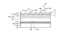
- the light-emitting element 10 is an element having a rectangular flat plate structure and includes an organic EL element 140.
- the organic EL element 140 includes at least a first electrode layer 141, a light emitting layer 142, and a second electrode layer 143 in this order, and can emit light from at least one of the surfaces 144 and 145. ing.
- the first electrode layer 141 is a transparent electrode layer
- the second electrode layer 143 is a reflective electrode layer.
- the light generated in the light emitting layer 142 is transmitted through the first electrode layer 141, or is reflected by the second electrode layer 143 and then transmitted through the light emitting layer 142 and the first electrode layer 141. Emanating from the surface 144. Therefore, in the following description, the surface 144 is referred to as a “light emitting surface”.
- the light emitting surface 144 of the organic EL element 140 is provided with a light emitting surface structure layer 100 as a structure layer according to the present invention.
- a light emitting surface structure layer 100 is directly provided so as to be in contact with the light emitting surface 144.
- the light emitting surface structure layer 100 may be provided indirectly on the light emitting surface 144 via a layer such as an adhesive layer or a light diffusion layer.
- the light emitting device 10 of the present embodiment may include a component other than the above-described members.
- the sealing substrate 151 is provided on the lower surface 145 of the organic EL element 140 in the drawing.
- an arbitrary substance such as a filler or an adhesive may exist between the surface 145 and the sealing substrate 151, or a gap may exist.
- air or other gas may be present in the space, or the space may be evacuated.
- the light emitting element 10 includes the sealing substrate 151, the organic EL element 140, and the light emitting surface structure layer 100 in this order, and can emit light through the surface 10U on the opposite side of the light emitting surface structure layer 100 from the organic EL element 140. It is like that.
- the surface 10U is located on the outermost side of the light emitting element 10, and light is emitted to the outside of the light emitting element 10 through the surface 10U. Therefore, the surface 10U is referred to as a “light emitting surface”.
- the organic EL element 140 is usually composed of two or more electrode layers and a light emitting layer that is provided between these electrode layers and emits light when a voltage is applied from the electrode layers. .
- An organic EL element forms layers such as an electrode layer and a light emitting layer constituting the organic EL element on a substrate, and further provides a sealing member that covers those layers, and a layer such as a light emitting layer is formed between the substrate and the sealing member.
- a sealed configuration is used.
- the organic EL element which emits light from the substrate side here is called a bottom emission type
- the organic EL element which emits light from the sealing member side is called a top emission type. Any of these may be sufficient as the organic EL element 140 provided in the light emitting element 10.
- FIG. In the case of the bottom emission type, a combination of the above-described substrate and an optional layer as necessary constitutes the light-emitting surface structure layer.
- a combination including a structure on the light exit surface side such as a sealing member and an optional layer as necessary constitutes the light exit surface structure layer.
- the light emitting layer is not particularly limited, and a known layer can be appropriately selected.
- the light emitting material in the light emitting layer is not limited to one type, and two or more types may be used in combination at any ratio.
- the light emitting layer is not limited to a single layer, and may be a single type of layer or a combination of a plurality of types of layers in order to suit the use as a light source. Thereby, the light of white or a color close thereto may be emitted.
- the electrode layer of the organic EL element is not particularly limited and can be appropriately selected from known ones.
- the electrode layer 141 on the light exit surface structure layer 100 side is a transparent electrode layer
- the electrode layer 143 on the opposite side is a reflective electrode layer, whereby the light exit surface structure layer 100 is formed. It is good also as an organic EL element which emits light from the light emission surface 144 toward.
- a reflecting member or a scattering member for example, a white scattering member disposed via an air layer
- the organic EL element 140 includes other layers such as a hole injection layer, a hole transport layer, an electron transport layer, and an electron injection layer (not shown) between the electrode layer 141 and the electrode layer 143. May be further included. Further, the organic EL element 140 may further include arbitrary components such as a wiring for energizing the electrode layers 141 and 143 and a peripheral structure for sealing the light emitting layer 142.
- Examples of the material for the transparent electrode layer include ITO (indium tin oxide).
- Examples of the material for the hole injection layer include a starburst aromatic diamine compound.
- Examples of the material for the hole transport layer include a triphenyldiamine derivative.
- a host material of a yellow light emitting layer a triphenyldiamine derivative etc. can be mentioned, for example,
- a dopant material of a yellow light emitting layer a tetracene derivative etc. can be mentioned, for example.
- Examples of the material for the green light emitting layer include pyrazoline derivatives.
- Examples of the host material for the blue light emitting layer include anthracene derivatives and the like, and examples of the dopant material for the blue light emitting layer include perylene derivatives.
- Examples of the material for the red light emitting layer include a europium complex.
- Examples of the material for the electron transport layer include an aluminum quinoline complex (Alq).
- As a material of the reflective electrode layer for example, lithium fluoride and aluminum can be used, which are sequentially laminated by vacuum film formation.
- a light emitting layer that generates a light emission color having a complementary color relationship which is called a laminated type or a tandem type, can be obtained by appropriately combining the above or other light emitting layers.
- the combination of complementary colors may be, for example, yellow / blue or green / blue / red.
- the light emitting surface structure layer 100 is a layer provided on the light emitting surface 144 of the organic EL element 140, and the surface of the light emitting surface structure layer 100 opposite to the organic EL element 140 is the light emitting surface 10U.
- the light exit surface 10U is a surface exposed on the outermost surface of the light emitting element 10, and is a light exit surface as the light emitting element 10, that is, a light exit surface when light is emitted from the light emitting element 10 to the outside of the apparatus.
- the light exit surface 10 ⁇ / b> U is a surface parallel to the light emitting surface 144 of the organic EL element 140 and parallel to the main surface of the light emitting element 10.
- the light exit surface 10U has an uneven structure when viewed microscopically, a portion corresponding to the surface of the concave portion or the convex portion can form an angle that is not parallel to the light emitting surface 144. Therefore, in the following description, being parallel or perpendicular to the light exit surface means that it is parallel or perpendicular to the light exit surface viewed macroscopically ignoring the recesses or projections unless otherwise specified.
- the light emitting element 10 will be described in a state where the light emitting surface 10U is placed so as to be parallel and upward with respect to the horizontal direction unless otherwise specified. Further, the fact that the component is “parallel” or “vertical” may include an error within a range that does not impair the effects of the present invention, for example, ⁇ 5 °. Further, “along” in a certain direction means “in parallel” in a certain direction unless otherwise specified.
- the light exit surface structure layer 100 includes a multilayer body 110 including the concavo-convex structure layer 111 and the base film layer 112, a support substrate 131 as a substrate, and an adhesive layer 121 that adheres the multilayer body 110 and the support substrate 131.
- the uneven structure layer 111 is a layer located on the upper surface of the light emitting element 10 (that is, the outermost layer on the light emitting surface side of the light emitting element 10).
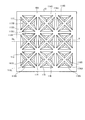
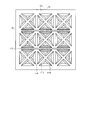
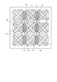
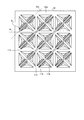
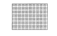
- the uneven structure layer 111 has an uneven structure including a first row 113, a second row 114, a third row 115, and a fourth row 116.
- the “row” means a group of a plurality of rows of recesses or projections extending continuously for a certain length in a certain direction.
- the direction in which the line extends means the direction in which the concave part or the convex part included in the line extends.
- the row may include, for example, only concave portions formed in a groove shape, for example, may include only convex portions formed in a bowl shape, or may include a combination thereof.
- each of the first to fourth strips 113 to 116 is a convex portion that protrudes relatively from the surroundings. For this reason, a recessed portion 117 that is relatively recessed exists at a position between the first to fourth rows 113 to 116.
- the concavo-convex structure includes the first to fourth rows 113 to 116 made of convex portions and the concave portion 117, and the outgoing surface 10U is defined by the concavo-convex structure. Yes.
- the number of convex portions included in the first to fourth rows 113 to 116 shown on the light exit surface 10U is only a small number. In an actual light emitting element, a much larger number of convex portions may be provided on the light emitting surface 10U of one light emitting element.
- FIG. 3 to 7 are plan views schematically showing an enlarged view of the light exit surface 10U of the light emitting element 10 according to the first embodiment of the present invention as viewed from the thickness direction of the light emitting element 10.
- FIG. 8 is a portion schematically showing a cross section of a part of the concavo-convex structure layer 111 according to the first embodiment of the present invention cut by a plane including the line 3a of FIG. 3 and perpendicular to the light exit surface 10U. It is sectional drawing.
- FIG. 8 is a portion schematically showing a cross section of a part of the concavo-convex structure layer 111 according to the first embodiment of the present invention cut by a plane including the line 3a of FIG. 3 and perpendicular to the light exit surface 10U. It is sectional drawing.
- the line 3 a passes through the point X where the third row 115 and the fourth row 116 intersect and the recess 117, and is parallel to the direction in which the first row 113 extends. It is.
- the first row 113 is hatched
- the second row 114 is hatched
- the third row 115 is hatched in FIG.
- the fourth row 116 is indicated by hatching.
- “thickness direction” represents the thickness direction of the light emitting element 10 unless otherwise specified.
- the light-emitting surface structure layer 100 includes four rows extending on the light-emitting surface 10U in a direction parallel to the light-emitting surface 10U, that is, a first row 113 and a second row. 114, a third row 115 and a fourth row 116.
- the first row 113, the second row 114, the third row 115, and the fourth row 116 all extend in a direction parallel to the light exit surface 10U.
- the directions in which the first row 113, the second row 114, the third row 115, and the fourth row 116 extend are not parallel to each other but intersect each other.
- the direction in which the first row 113 extends is the first direction
- the second row 114 extends in the second direction intersecting the first direction
- the third row 115 extends in a third direction intersecting the first direction and the second direction
- the fourth row 116 is a fourth direction intersecting the first direction, the second direction, and the third direction. It extends in the direction.
- the angles formed by the directions may be arbitrarily set as long as the effects of the present invention are not significantly impaired.
- the direction in which each row 113 to 116 extends is usually 4 ° or more, preferably 15 ° or more, more preferably 22.5 ° or more, and usually 176 ° or less, preferably 165 ° or less.
- a range of 180 ° / N ⁇ (m ⁇ 1) ⁇ 180 ° / 1.1N is preferable, The range of 180 ° / N ⁇ (m ⁇ 1) ⁇ 180 ° / 1.5N is more preferable, A range of 180 ° / N ⁇ (m ⁇ 1) ⁇ 180 ° / 2N is particularly preferable.
- m represents an integer of 1 or more and N or less.
- the general formula represents an angle formed by the reference direction and a direction in which the m-th row extends when a certain reference direction is set to an angle of 0 °.
- the first row 113 is formed so as to extend in a first direction Di parallel to the light exit surface 10U.
- the second row 114 extends in a second direction Dii that forms an angle ⁇ 1 with respect to the first direction Di in which the first row 113 extends. Is formed.
- the third row 115 extends in a third direction Diii that forms an angle ⁇ 2 with respect to the first direction Di in which the first row 113 extends. Is formed.
- the fourth row 116 extends in a fourth direction Div that forms an angle ⁇ 3 with respect to the first direction Di in which the first row 113 extends. Is formed.
- angles ⁇ 1 to ⁇ 3 may be larger than 0 ° and smaller than 180 °, but it is usually from the viewpoint of effectively suppressing the rainbow unevenness and the change in appearance due to the azimuth angle at which the observer looks at the light emitting element. Is 4 ° or more and less than 176 °. However, the angles ⁇ 1 to ⁇ 3 are different from each other, and are preferably different from each other by 4 ° or more as described above. In the present embodiment, ⁇ 1 is set to 90 °, ⁇ 2 is set to 45 °, and ⁇ 3 is set to 135 °.
- the shape of the cross section obtained by cutting the first to fourth strips 113 to 116 along a plane orthogonal to the direction in which the strips 113 to 116 extend may be, for example, a rectangle or a semicircle.
- the above polygon is preferable. This is because the polygonal shape is easy to mold and the rows 113 to 116 can be easily molded, and the target optical characteristics strongly depend on the angles of the inclined surfaces 113S to 116S.
- the target optical characteristics strongly depend on the angles of the inclined surfaces 113S to 116S.
- the angle of the inclined surfaces 113S to 116S is easy to collect when the angle of the inclined surfaces 113S to 116S is around 45 °. It is said that it is easy to make uniform.
- the shape of the cross section of the row means the shape of the concave portion or the convex portion (the convex portion in the present embodiment) constituting the row in the cross section of the row.
- the shape of the cross section obtained by cutting the first to fourth strips 113 to 116 along a plane orthogonal to the direction in which the strips 113 to 116 extend is Is also a trapezoid (specifically an isosceles trapezoid) that is a square. Therefore, as shown in FIG. 1, each of the first to fourth rows 113 to 116 has flat portions 113U to 116U as the most projecting portions, and the flat portions 113U to 116U have the upper base of the trapezoid. It corresponds to.
- the first to fourth strips 113 to 116 have a pair of slopes 113S to 116S corresponding to opposite sides of the trapezoid, and the flat portions 113U to 116U are sandwiched between the slopes 113S to 116S. It is supposed to be.
- the “slope” is a surface that is inclined with respect to the light exit surface 10U, that is, a surface that forms an angle that is not parallel to the light exit surface 10U.
- the angle of the slope is an angle formed by the slope with respect to the light exit surface 10U.
- the surfaces on the flat portions 113U to 116 are parallel and flat with respect to the light exit surface 10U.
- the flat portions 113U to 116U have an effect of improving the durability of the uneven structure, and, for example, emit light emitted from the organic EL element 140 and repeatedly reflected until extracted in the air in various directions. Reflecting has the effect of increasing the light extraction efficiency.
- each of the first to fourth rows 113 to 116 includes a plurality of convex portions, and these convex portions are provided at predetermined intervals. For this reason, a recess 117 that is relatively recessed from the periphery exists between the rows 113 to 116. That is, the light exit surface 10U is provided with a plurality of recesses 117, and each recess 117 is discretely formed by being separated by the rows 113 to 116. As shown in FIG. 8, the bottom of the recess 117 is a flat portion 117B that is a flat surface parallel to the light exit surface 10U. If dust and debris accumulate in the recess 117, the light extraction efficiency may be reduced and a bright spot may be generated. However, since the bottom of the recess 117 is a flat flat portion 117B, In addition, it is possible to make it difficult to collect debris and the like.
- the dimensions such as the height H, width W, and pitch P of the recesses or projections included in the respective rows 113 to 116 do not significantly impair the effects of the present invention.
- the height H is usually 1 ⁇ m or more, preferably 2 ⁇ m or more, and is usually 50 ⁇ m or less, preferably 40 ⁇ m or less.
- the width W is usually 1 ⁇ m or more, preferably 2 ⁇ m or more, and is usually 60 ⁇ m or less, preferably 50 ⁇ m or less.
- the pitch P is usually 0.5 ⁇ m or more, preferably 1 ⁇ m or more, and is usually 2 mm or less, preferably 1 mm or less.
- the dimensions such as the height H, the width W, and the pitch P may be constant, for example, depending on the position in the extending direction. May change.
- the dimension of the convex portion is assumed to be constant in the extending direction.
- the dimensions of the recesses or projections included in the same row 113 to 116 may be the same or different.
- the dimensions of the recesses or protrusions included in the different rows 113 to 116 may be the same or different.
- the height H and the width W of the convex portions are constant in any of the rows 113 to 116.
- the size of the pitch P is adjusted so that any of the third row 115 and the fourth row 116 pass through the point where the first row 113 and the second row 114 intersect. .
- the shape of the recess 117 viewed from the thickness direction is the same in any of the recesses 117, and the flat portion 117B at the bottom of each recess 117 is a triangle.
- the average angle (hereinafter referred to as “average inclination angle”) ⁇ formed by the slopes 113S to 116S of the first to fourth rows 113 to 116 with respect to the flat portions 113U to 116U (and hence the light exit surface 10U) is as follows. If it is in the range of 45 ° ⁇ 10 °, it is suitable for condensing light in the front direction. On the other hand, in order to suppress a change in color depending on the observation angle, 55 ° or more is preferable, 60 ° or more is more preferable, 85 ° or less is preferable, and 70 ° or less is more preferable.
- the light extraction efficiency can be increased while suppressing the rainbow unevenness by suppressing the change in the tint due to the observation angle (polar angle). Further, the durability of the concavo-convex structure layer 111 can be improved by setting the average inclination angle ⁇ of the slopes 113S to 116S to be equal to or less than the upper limit of the above range.
- the angles formed by all the slope portions 113S to 116S with respect to the light exit surface 10U are set to the same size, but may be different.
- the light extraction efficiency of the light emitting element 10 can be improved by appropriately adjusting the “flat portion ratio”. Specifically, by setting the flat portion ratio to 10% to 75%, good light extraction efficiency can be obtained, and the mechanical strength of the light exit surface 10U can be increased.
- the thickness T of the concavo-convex structure layer 111 shown in FIG. 8 may be set in an appropriate range in relation to the height H of the concave or convex portions included in the first to fourth rows 113 to 116.
- the flexibility of the light emitting element 10 is improved by reducing the thickness T of the uneven structure layer 111. This makes it possible to easily handle the uneven structure layer 111 in the manufacturing process of the light emitting element 10, which is preferable.
- the difference between the height H of the recesses or projections included in the rows 113 to 116 and the thickness T of the uneven structure layer 111 is preferably 0 to 30 ⁇ m.
- the light exit surface structure layer 100 may be composed of a plurality of layers, but may be composed of a single layer. From the viewpoint of easily obtaining the light-emitting surface structure layer 100 having desired characteristics, it is preferable that the light-emitting surface structure layer 100 is composed of a plurality of layers.
- the light exit surface structure layer 100 includes a multilayer body 110 in which an uneven structure layer 111 and a base film layer 112 are combined. Thereby, the light emission surface structure layer 100 with high performance can be obtained easily.
- the concavo-convex structure layer 111 and the base film layer 112 are usually formed of a resin composition containing a transparent resin.
- the transparent resin is “transparent” means having a light transmittance suitable for use in an optical member.
- each layer constituting the light exit surface structure layer 100 may have a light transmittance suitable for use in an optical member.
- the light exit surface structure layer 100 as a whole has a total light beam of 80% or more. What is necessary is just to have the transmittance
- the transparent resin contained in the resin composition is not particularly limited, and various resins that can form a transparent layer can be used.
- various resins that can form a transparent layer can be used.
- examples thereof include a thermoplastic resin, a thermosetting resin, an ultraviolet curable resin, and an electron beam curable resin.
- thermoplastic resins are preferable because they can be easily deformed by heat, and ultraviolet curable resins have high curability and high efficiency, so that the uneven structure layer 111 can be efficiently formed.
- thermoplastic resin examples include polyester-based, polyacrylate-based, and cycloolefin polymer-based resins.
- ultraviolet curable resin examples include epoxy resins, acrylic resins, urethane resins, ene / thiol resins, and isocyanate resins. As these resins, those having a plurality of polymerizable functional groups can be preferably used. In addition, the said resin may be used individually by 1 type, and may be used combining two or more types by arbitrary ratios.
- the material of the concavo-convex structure layer 111 constituting the multilayer body 110 a material having a high hardness at the time of curing from the viewpoint of easily forming the concavo-convex structure of the light exit surface 10U and easily obtaining the scratch resistance of the concavo-convex structure.
- a material having a pencil hardness of HB or higher is preferable, and a material of H or higher is more preferable.
- the material which becomes 2H or more is more preferable.
- the material of the base film layer 112 in order to facilitate the handling when forming the concavo-convex structure layer 111 and the handling of the multilayer body 110 after forming the multilayer body 110, a certain degree of flexibility is provided. There are preferred. By combining such materials, the multilayer body 110 that is easy to handle and excellent in durability can be obtained, and as a result, the high-performance light-emitting element 10 can be easily manufactured.
- Such a combination of materials can be obtained by appropriately selecting the transparent resin exemplified above as a resin constituting each material.
- a resin constituting each material for example, an ultraviolet curable resin such as acrylate is used, while as the transparent resin constituting the material of the base film layer 112, for example, an alicyclic olefin It is preferable to use a polymer film (for example, ZEONOR film manufactured by Nippon Zeon Co., Ltd.) or a polyester film.
- the refractive index of the concavo-convex structure layer 111 and the base film layer 112 may be as close as possible.
- the refractive index difference between the uneven structure layer 111 and the base film layer 112 is preferably within 0.1, and more preferably within 0.05.
- a material of a layer that is a constituent element of the light exit surface structure layer 100 such as the concavo-convex structure layer 111 and the base film layer 112
- a material having light diffusibility may be used. Thereby, since the light which permeate
- the light diffusing material examples include a material containing particles, and an alloy resin that diffuses light by mixing two or more kinds of resins.
- a material including particles is preferable, and a resin composition including particles is particularly preferable.
- the particles may be transparent or opaque.
- the material of the particles include metals and metal compounds, and resins.
- the metal compound include metal oxides and nitrides. Specific examples of metals and metal compounds include metals having high reflectivity such as silver and aluminum; metal compounds such as silicon oxide, aluminum oxide, zirconium oxide, silicon nitride, tin-added indium oxide, and titanium oxide. be able to.
- the resin include methacrylic resin, polyurethane resin, and silicone resin.
- grain material may be used individually by 1 type, and may be used combining two or more types by arbitrary ratios.
- the shape of the particles can be, for example, a spherical shape, a cylindrical shape, a needle shape, a cubic shape, a rectangular parallelepiped shape, a pyramid shape, a conical shape, a star shape, or the like.
- the particle diameter of the particles is preferably 0.1 ⁇ m or more, preferably 10 ⁇ m or less, more preferably 5 ⁇ m or less.
- the particle diameter is a 50% particle diameter in an integrated distribution obtained by integrating the volume-based particle amount with the particle diameter as the horizontal axis. The larger the particle size, the larger the content ratio of particles necessary for obtaining the desired effect, and the smaller the particle size, the smaller the content.
- the particle size is smaller, desired effects such as a reduction in change in color depending on the observation angle and an improvement in light extraction efficiency can be obtained with fewer particles.
- the particle shape is other than spherical, the diameter of the sphere having the same volume is used as the particle size.
- the difference between the refractive index of the particles and the refractive index of the transparent resin is preferably 0.05 to 0.5. More preferably, it is 07 to 0.5.
- either the particle or the refractive index of the transparent resin may be larger. If the refractive index of the particles and the transparent resin is too close, the diffusion effect cannot be obtained and the color unevenness may be difficult to be suppressed. Conversely, if the difference is too large, the diffusion becomes large and the color unevenness is suppressed, but light Extraction effect may be reduced.
- the content ratio of the particles is a volume ratio in the total amount of the layer containing the particles, preferably 1% or more, more preferably 5% or more, 80% or less, and more preferably 50% or less.
- the resin composition can contain arbitrary components as necessary.
- the optional component include additives such as phenol-based and amine-based deterioration preventing agents; surfactant-based, siloxane-based antistatic agents; triazole-based, 2-hydroxybenzophenone-based light-resistant agents; Can be mentioned.
- the thickness T of the uneven structure layer 111 is not particularly limited, but is preferably 1 ⁇ m to 70 ⁇ m.
- the thickness T of the concavo-convex structure layer 111 is the distance between the surface on the base film layer 112 side where the concavo-convex structure is not formed and the flat portions 113U to 116U of the concavo-convex structure.
- the thickness of the base film layer 112 is preferably 20 ⁇ m to 300 ⁇ m.
- the light emitting element 10 of this embodiment includes a support substrate 131 between the organic EL element 140 and the multilayer body 110.
- the support substrate 131 By providing the support substrate 131, the light emitting element 10 can be given rigidity for suppressing deflection.
- the supporting substrate 131 is provided with a substrate that is excellent in the performance of sealing the organic EL element 140 and that can easily form the layers constituting the organic EL element 140 on the manufacturing process in order. As a result, the durability of the light emitting element 10 can be improved and the manufacture can be facilitated.
- Examples of the material constituting the support substrate 131 include glass and resin. In addition, the material of the support substrate 131 may be used individually by 1 type, and may be used combining two or more types by arbitrary ratios.
- the refractive index of the support substrate 131 is not particularly limited, but is preferably 1.4 to 2.0.
- the thickness of the support substrate 131 is not particularly limited, but is preferably 0.1 mm to 5 mm.
- the light emitting element 10 of this embodiment includes an adhesive layer 121 between the multilayer body 110 and the support substrate 131.
- the adhesive layer 121 is a layer that is interposed between the base film layer 112 of the multilayer body 110 and the support substrate 131 and adheres these two layers.
- the adhesive that is the material of the adhesive layer 121 is not only a narrowly defined adhesive (a so-called hot-melt type adhesive having a shear storage modulus at 23 ° C. of 1 to 500 MPa and not exhibiting tackiness at room temperature), A pressure-sensitive adhesive having a shear storage modulus at 23 ° C. of less than 1 MPa is also included.
- a material having a refractive index close to that of the support substrate 131 or the base film layer 112 and transparent can be used as appropriate. More specifically, an acrylic adhesive or a pressure-sensitive adhesive can be used.
- the thickness of the adhesive layer is preferably 5 ⁇ m to 100 ⁇ m.
- each layer constituting the organic EL element 140 is laminated on one surface of the support substrate 131, and after or before that, the other surface of the support substrate 131 is uneven.
- the multi-layer body 110 having the structural layer 111 and the base film layer 112 can be manufactured by sticking via the adhesive layer 121.
- a mold such as a mold having a desired shape is prepared, and this mold is a layer of a material for forming the concavo-convex structure layer 111.
- Method 1 An unprocessed multilayer having a layer of the resin composition A constituting the base film layer 112 and a layer of the resin composition B constituting the concavo-convex structure layer 111 (the concavo-convex structure is not yet formed) A method for preparing and forming a concavo-convex structure on the surface of the raw multilayer body on the resin composition B side; and (Method 2) applying the resin composition B in a liquid state on the base film layer 112 Then, a method may be mentioned in which a mold is applied to the applied layer of the resin composition B, the resin composition B is cured in that state, and the concavo-convex structure layer 111 is formed.
- the raw multilayer body can be obtained by, for example, extrusion molding in which the resin composition A and the resin composition B are coextruded.
- An uneven structure can be formed by pressing a mold having a desired surface shape onto the surface of the unprocessed multilayer body on the resin composition B side. More specifically, a long raw multilayer body is continuously formed by extrusion molding, and the raw multilayer body is pressed with a transfer roll and a nip roll having a desired surface shape, thereby continuously. Manufacturing can be performed efficiently.
- the clamping pressure between the transfer roll and the nip roll is preferably several MPa to several tens of MPa.
- the temperature at the time of transfer is preferably Tg or more (Tg + 100 ° C.) or less, where Tg is the glass transition temperature of the resin composition B.
- the contact time between the unprocessed multilayer body and the transfer roll can be adjusted by the film feed speed, that is, the roll rotation speed, and is preferably 5 seconds or more and 600 seconds or less.
- Method 2 it is preferable to use a composition that can be cured by energy rays such as ultraviolet rays as the resin composition B constituting the concavo-convex structure layer 111.
- the resin composition B is applied on the base film layer 112, and with the mold applied, an energy beam such as ultraviolet rays is irradiated from a light source located on the back side of the application surface to cure the resin composition B.
- the coating film of the resin composition B is used as the concavo-convex structure layer 111, and the multilayer body 110 can be obtained.
- the back side of the coated surface refers to the side of the base film opposite to the surface coated with the resin composition B.
- the light emitting element 10 of the present embodiment Since the light emitting element 10 of the present embodiment is configured as described above, the light emitted from the light emitting surface 144 of the organic EL element 140 passes through the light emitting surface structure layer 100 and is extracted from the light emitting surface 10U. At this time, since the light exit surface 10U has a concavo-convex structure including the first to fourth strips 113 to 116 and the concave portion 117, even the light that cannot be extracted from the flat portions 113U to 116U and 117B is emitted from the inclined surfaces 113S to 116S. Since the light can be extracted, the light extraction efficiency from the light output surface 10U can be increased as compared with the case where the uneven structure is not provided.
- the light emitting element 10 has the first to fourth rows 113 to 116 on the light exit surface 10U, the rainbow unevenness is small, and the variation in the appearance due to the azimuth angle at which the observer views the light emitting element is small. .
- the reason why such an effect is obtained is not clear, but according to the study of the present inventor, it is presumed that the reason is as follows.
- the optical characteristics observed at the azimuth angle according to the azimuth angle to be observed ( It is thought that brightness, color, etc.) were greatly different, and the change in appearance due to the azimuth angle was large.
- the rows 113 to 116 extending in three or more different directions are provided on the light exit surface 10U as in the present embodiment, the regularity of the concavo-convex structure of the light exit surface 10U is lowered, and from which azimuth angle Even if observed, the optical characteristics do not differ so much, and it is assumed that the appearance by the azimuth is uniform.
- the light exit surface has a flat surface
- unevenness may be observed on the light exit surface due to interference of light reflected on the flat surface.
- strips 113 to 116 extending in three or more different directions are provided on the light exit surface 10U as in this embodiment, the interference due to the flat portions 113U to 116U and 117B is dispersed, and unevenness due to the interference is reduced. Expression can be suppressed.
- the light emitting element 10 of the present embodiment it is possible to prevent the light exit surface 10U from being chipped due to an external impact, and as a result, the mechanical strength of the light exit surface 10U can be improved.
- the light emitting device 10 of the present embodiment has flat portions 113U to 116U that are flat at the outermost position in the thickness direction. For this reason, it is possible to prevent the force from being concentrated on a part of the concavo-convex structure layer 111 due to the force or impact applied to the light exit surface 10U from the outside.
- the mechanical strength of 10 can be increased.
- the uneven structure on the light exit surface may have three or more different heights. However, it is preferable that the height of the concavo-convex structure is different from each other by 0.1 ⁇ m or more, regardless of the height.
- the uneven structure of the light exit surface has three or more heights that differ by 0.1 ⁇ m or more, the uneven structure of the light exit surface is one or both of the outgoing light that exits through the light exit surface and the reflected light that is reflected by the light exit surface. It will have a dimensional difference that exceeds the difference that causes interference. Thereby, the rainbow nonuniformity by interference of the one or both of the said emitted light and reflected light can be suppressed effectively.
- the height difference of the concavo-convex structure may be, for example, 0.15 ⁇ m or more or 0.2 ⁇ m or more in addition to 0.1 ⁇ m or more.
- the upper limit of the height difference of the concavo-convex structure is not particularly limited, but if it is too large, the light emitting element tends to be thick. Therefore, the upper limit of the height difference of the concavo-convex structure is preferably 50 ⁇ m or less, for example 25 ⁇ m. Or 10 ⁇ m or less.
- the height of the concavo-convex structure means the position in the thickness direction of the light exit surface other than the slope, and usually the position in the thickness direction of the most protruding portion of the convex part included in the line, and the line
- the position in the thickness direction of the bottom of the recessed part provided between the convex parts contained is said.
- not only the light emitted by the organic EL element but also the light emitted from the light emitting surface enters the light emitting element from the light emitting surface, is reflected inside the light emitting element, and passes again through the light emitting surface. Including light that is emitted.
- the example is demonstrated using drawing.
- FIG. 9 shows the light emitting device 20 according to the second embodiment of the present invention, in which the first row 113 extends through the point where the third row 115 and the fourth row 116 intersect and the recess 117.
- It is sectional drawing which shows typically the cross section cut
- the element similar to 1st embodiment is shown with the code
- the light emitting element 20 according to the second embodiment of the present invention includes the height of the convex portions included in the first row 113 (see FIG. 1) and the second row 114, and the third row. Except that the heights of the convex portions included in the first row 115 and the fourth row 116 are different, the light emitting element 10 according to the first embodiment has the same configuration. Specifically, the height of the convex portion included in the third row 115 and the fourth row 116 is higher than the height of the convex portion included in the first row 113 and the second row 114. It is low.
- the height T I represents the position in the thickness direction of the flat portion 117B at the bottom of the recess 117.
- the height T II represents the position in the thickness direction of the flat portion 116U of the third flat portion 115U of the ridges 115 and the fourth ridges 116.
- the height T III represents the position in the thickness direction of the flat portion 113U of the first row 113 and the flat portion 114U of the second row 114.
- line 116 is set to 0.1 micrometer or more. Furthermore, the difference between the height of the convex portion included in the first row 113 and the second row 114 and the height of the convex portion included in the third row 115 and the fourth row 116 is also 0. It is set to 1 ⁇ m or more. Accordingly, the three heights T I to T III of the uneven structure of the light exit surface 10U are different from each other by 0.1 ⁇ m or more.
- the difference between the three heights T I to T III of the concavo-convex structure of the light exit surface 10U is a dimensional difference of the concavo-convex structure exceeding the difference that causes interference of one or both of the emitted light and the reflected light. Unevenness can be suppressed. That is, interference between the emitted light and reflected light at the flat portions 113U and 114U, the flat portions 115U and 116U, and the flat portions 117B located at different heights can be suppressed, and rainbow unevenness can be effectively suppressed.
- the dimensional differences T III -T II and T II -T I are effective even when the dimensional difference exceeds the difference that causes interference of the outgoing light, but usually the reflected light is more than the outgoing light. Since there is a tendency that the influence on the rainbow unevenness is greater, the dimensional difference exceeding the difference that causes interference of reflected light exhibits a remarkable effect.
- the dimensional difference exceeding the difference that causes the interference is, for example, interference of outgoing light emitted from the organic EL element 140, for example, usually 0.62 times or more of the center wavelength of outgoing light, preferably 1 Dimensional difference more than 5 times.
- the upper limit of the dimensional difference is not particularly limited, but is preferably 60 times or less of the center wavelength of the emitted light.
- the dimensional difference exceeding the difference that causes interference is usually 0.62 times or more, preferably 1.5 times or more the center wavelength of transmitted light and reflected light. And a dimensional difference of usually 60 times or less.
- transmitted light and reflected light are natural light and include light having an arbitrary wavelength, it is difficult to determine the center wavelength of the reflected light. Therefore, in view of the fact that the light that causes rainbow unevenness is visible light, the above-mentioned dimensional difference may be set as the center wavelength of light that normally reflects the center wavelength of visible light of 550 nm.
- the concavo-convex structure has three or more heights T I , T II and T III different from each other by 0.1 ⁇ m or more as in the present embodiment, the same advantages as those of the first embodiment can be obtained.
- the heights H of the convex portions included in all the rows 113 to 116 can be made uniform as in the first embodiment, rainbow unevenness due to interference is unlikely to occur, but in actual products, manufacturing of temperature, humidity, etc. It may be difficult to make the height H of the convex portions included in the rows 113 to 116 highly uniform due to the change of the conditions. Therefore, by making the uneven structure positively have different heights T I , T II and T III as described above, rainbow unevenness can be more easily suppressed.
- FIG. 10 is a perspective view schematically showing a light emitting device according to the third embodiment of the present invention.
- the same elements as those in the first embodiment are denoted by the same reference numerals as those in the first embodiment.
- the organic EL element 340 includes a second electrode layer 343 that is a transparent electrode instead of the second electrode layer 143 that is a reflective electrode. And it has the same structure as 1st embodiment except the point where the light emission surface structure layer 100 is provided instead of the sealing substrate 151.
- an arbitrary substance such as a filler or an adhesive may exist between the light emitting surface structure layer 100 on the lower side in the drawing and the second electrode 343, and a void exists. Also good. As long as there is no inconvenience such as greatly impairing the durability of the light emitting layer 142, air or other gas may be present in the space, or the space may be evacuated.
- the second electrode layer 343 is a transparent electrode, the light from the light emitting layer 142 is transmitted through the first electrode layer 141 and the second electrode layer 343, and both the upper and lower light exit surfaces in the figure. Light exits through 10U. Accordingly, the lower surface 345 of the organic EL element 340 also functions as a light emitting surface. Even when light is emitted through both the front surface and the back surface, advantages similar to those of the first embodiment can be obtained.
- the light incident on one light exit surface 10U usually passes through the light emitting element 30 and exits through the other light exit surface 10U. Accordingly, the opposite side can be seen with the naked eye through the light emitting element 30, and a see-through light emitting element can be realized, so that the design can be diversified.
- a see-through type light emitting element transparency is required, so the optimum value such as the angle of the slope is different from that in the first embodiment, and the number of rows is preferably 4 groups or more, 6 groups or more are more preferable.
- the lower limit of the angle of the slope of the row (which may be an average inclination angle) is preferably 70 ° or more, more preferably 80 ° or more, and the upper limit is preferably 87.5 ° or less, more preferably 85 ° or less. If the angle is too small, the haze increases, and if it is too large, the take-out efficiency decreases and the workability may deteriorate.
- the light emitting surface structure layer 100 is provided so as to be in direct contact with the light emitting surface 144 in the above-described embodiment, the light emitting surface structure layer 100 may be provided on the light emitting surface 144 via another layer.
- the other layers include a gas barrier layer that protects the organic EL element 140 from the outside air and moisture, and an ultraviolet cut layer that blocks ultraviolet rays.
- the light exit surface structure layer 100 includes the uneven structure layer 111, the base film layer 112, the adhesive layer 121, and the support substrate 131. These layers may be composed of fewer layers than these, or conversely may include any layers in addition to these layers.
- a coating layer may be further provided on the surface of the concavo-convex structure layer 111, and this may define the concavo-convex structure of the light exit surface 10U.
- any third row 115 and fourth row 116 pass through a point where the first row 113 and the second row 114 intersect.
- the first to fourth rows 113 to 116 intersect at one intersection.
- the first to fourth rows 113 to 116 may not intersect at one intersection.
- the width of the pitch of any row may be made non-uniform, or the position of the row or the extending direction may be shifted from the above-described embodiment.
- FIG. 11 is a plan view schematically showing an enlarged view of the light exit surface 10U of the light emitting element 40 according to the modification of the first embodiment of the present invention as viewed from the thickness direction of the light emitting element 40.
- the same elements as those of the first embodiment are denoted by the same reference numerals as those of the first embodiment.
- the first to fourth strips 113 to 116 each include a protruding portion that protrudes from the surroundings.
- the first to fourth strips are arranged from the surroundings. Also, it may include a depressed recess.
- column which consists of a recessed part may coexist on the same light-emitting surface.
- the concave portions or the convex portions included in the first to fourth rows may be formed in a shape with rounded corners.
- a light-emitting element having the same effect as the reflective electrode is configured even if the reflective electrode is replaced with a combination of a transparent electrode and a reflective layer. can do.
- column 114 is made high, and the convex part contained in the 3rd row
- the height is made lower so that the uneven structure of the light exit surface 10U has a different height, the uneven structure of the light output surface 10U may have a different height by other configurations. For example, only the convex portions included in the first strip 113 may be increased, and the convex portions included in the second to fourth strips 114 to 116 may be decreased.
- the position in the thickness direction of the flat portion 117B at the bottom of the concave portion 117 is made non-uniform so that the position of the flat portion 117B at the bottom of one concave portion 117 and the position of the flat portion 117B at the bottom of another concave portion 117
- the thickness direction may differ by 0.1 ⁇ m or more.
- the height of the convex portions belonging to the same row is made non-uniform, or the height of a certain convex portion is made non-uniform in the extending direction, so that the height of the uneven structure of the light exit surface 10U is different. You may give it.
- both the light emitting surfaces 144 and 345 of the organic EL element 340 are provided with the same light emitting surface structure layer 100 has been described. May be provided in combination. Further, in the double-sided light emitting element, as long as the light emitting surface structure layer is provided on at least one light emitting surface, the light emitting surface structure layer may not be provided on the other light emitting surface.
- the light-emitting device of the present invention can be used for applications such as lighting equipment and backlight devices.
- the luminaire includes the light-emitting element of the present invention as a light source, and further includes optional components such as a member for holding the light source and a circuit for supplying power as necessary.
- the backlight device includes the light emitting element of the present invention as a light source, and further includes a housing, a circuit for supplying power, a diffusion plate for making light emitted more uniform, a diffusion sheet, if necessary. It includes optional components such as a prism sheet.
- Applications of the backlight device include a display device such as a liquid crystal display device that displays an image by controlling pixels, and a backlight of a display device that displays a fixed image such as a signboard.
- a white organic EL element was prepared.
- the multilayer body was attached to the light emitting surface of the prepared organic EL element via an adhesive (acrylic resin, refractive index 1.49, CS9621 manufactured by Nitto Denko Corporation).
- an organic EL element, an adhesive layer, and a multilayer body were provided in this order, and a light emitting element having no uneven structure on the surface (light emitting surface) opposite to the organic EL element was obtained.
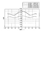
- the light emitting element was mounted on a rotatable support. Further, a spectral radiance meter (BM-5 manufactured by Topcon Corporation) was installed in front of the light emitting surface of the light emitting element (normal direction). In a state where light is emitted by applying a constant current of 100 mA / m 2 to the light emitting element, the light emitting element is rotated to change the observation direction of the spectral radiance meter with respect to the light emitting surface, and the chromaticity (x, y) and Luminance was measured. As shown in FIG.
- the observation direction is a normal direction of the light exit surface 50U with a certain direction in the surface of the light exit surface 50U as the x axis, a direction orthogonal to the x axis in the surface of the light exit surface 50U as the y axis.
- the polar angle ⁇ is in the range of ⁇ 85 ° to + 85 °.
- the measurement was performed twice, in which the azimuth angle ⁇ was 0 ° to 180 ° and 45 ° to 225 °.
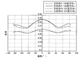
- the measurement result of chromaticity (x, y) is shown in FIG.
- FIG. 14 schematically shows a part of the concavo-convex structure layer produced in Comparative Example 1 as viewed from the thickness direction.
- the white part represents a flat part
- the hatched part represents a slope.
- the concavo-convex structure on the surface of the concavo-convex structure layer has two groups of rows extending in two directions perpendicular to each other in a plane parallel to the surface.
- a concave portion having a plurality of regular quadrangular pyramid shapes that is, a shape obtained by cutting the top portion of the quadrangular pyramid with a plane parallel to the bottom surface
- a flat portion positioned around the concave portion.
- each row includes a plurality of convex portions provided along a certain direction, and the cross-sectional shape cut by a plane orthogonal to the direction in which the row extends is a trapezoid,
- the inclination angles of the slopes included in the rows were all 60 °.
- the most protruding part of each row was a flat part, and the width of the flat part was 5 ⁇ m.
- the bottom of the concave portion was a square flat portion, and the length of the side of the square was 15 ⁇ m.
- the height of each convex portion was 9 ⁇ m.
- the obtained multilayer body was placed with the surface on which the concavo-convex structure was formed facing upward, and the surface on which the concavo-convex structure was formed was irradiated from a fluorescent lamp as a line light source.
- a fluorescent lamp as a line light source.
- the organic EL element, the adhesive layer, and the multilayer body are provided in this order in the same manner as in Reference Example 1 except that the multilayer body obtained in Comparative Example 1 was used as the multilayer body.
- a light emitting element having a concavo-convex structure on the surface (light emitting surface) was obtained.
- Example 1 Except that the shape of the metal mold was changed, a multilayer body which was a rectangular film having a layer structure of base film-uneven structure layer was obtained in the same manner as in Comparative Example 1.
- FIG. 16 schematically shows a part of the concavo-convex structure layer produced in Example 1 as viewed from the thickness direction.
- a white portion represents a flat portion
- a hatched portion represents a slope.
- the concavo-convex structure on the surface of the concavo-convex structure layer is 0 °, 40 °
- each strip includes a plurality of convex portions provided along a certain direction, and the cross-sectional shape cut by a plane orthogonal to the direction in which the strip extends extends is a trapezoid.
- the inclination angle of the slope included in each was 60 °.
- the most protruding part of each row was a flat part, and the width of the flat part was 5 ⁇ m.
- column was 35 micrometers in the row
- the height of each convex portion was 9 ⁇ m.
- the metal mold was produced by cutting a metal mold original plate in four azimuth directions with a cutting tool having two 60 ° inclination angles.
- the four azimuth directions are 0 °, 40 °, 90 °, and 130 ° directions
- the cutting width is 15 ⁇ m
- the cutting pitch is 35 ⁇ m in the azimuth angles 0 ° and 90 ° directions
- the azimuth angle is 40 °. It was set to 40 ⁇ m in the direction and 130 ° direction.
- the organic EL element, the adhesive layer, and the multilayer body were provided in this order in the same manner as in Reference Example 1 except that the multilayer body obtained in Example 1 was used as the multilayer body, and on the side opposite to the organic EL element.
- a light emitting element having a concavo-convex structure on the surface (light emitting surface) was obtained.
- chromaticity (x, y) and luminance were measured in the same manner as in Reference Example 1.
- the measurement result of chromaticity (x, y) is shown in FIG.
- the azimuth angle ⁇ was 45 ° to 225 °
- ( ⁇ x, ⁇ y) (0.018, 0.038).
- Example 1 the light extraction efficiency was improved compared to Reference Example 1, and the color change due to polar angle was improved. Furthermore, as shown in FIG. 17, at any polar angle, the chromaticity when the azimuth angle ⁇ is 0 ° to 180 ° and the chromaticity when the azimuth angle ⁇ is 45 ° to 225 °. It was almost the same. From this, it was confirmed that in Example 1, the degree of improvement in color change by the azimuth angle was about the same, and the change in appearance (particularly the change in tint) due to the azimuth angle was small.
- the organic EL element, the adhesive layer, and the multilayer body were provided in this order in the same manner as in Reference Example 1 except that the multilayer body obtained in Comparative Example 2 was used as the multilayer body, and on the side opposite to the organic EL element.
- a light emitting element having a concavo-convex structure on the surface (light emitting surface) was obtained.
- the film is a rectangular film having a layer structure of a base film-concave structure layer in the same manner as in Example 1 except that the slopes of the slopes are all changed to 45 °. A multilayer was obtained.
- the organic EL element, the adhesive layer, and the multilayer body were provided in this order in the same manner as in Reference Example 1 except that the multilayer body obtained in Example 2 was used as the multilayer body, and on the side opposite to the organic EL element.
- a light emitting element having a concavo-convex structure on the surface (light emitting surface) was obtained.
- Example 2 (Measurement of optical properties) Using the obtained light emitting device, luminance was measured in the same manner as in Reference Example 1. As a result of measurement, in Example 2, the light extraction efficiency was improved by 10% compared to Reference Example 1, and the front luminance was 1.35 times. From this, even when the inclination angle of the slope of the row is 45 °, it is understood that the effect of improving the front luminance can be obtained similarly to the case where the inclination angle is 60 ° as in Comparative Example 1. It was.
- the light-emitting element of the present invention can be used as a light source for any application, and is particularly suitable for use as a backlight for lighting equipment and display devices.
Landscapes
- Physics & Mathematics (AREA)
- Optics & Photonics (AREA)
- General Physics & Mathematics (AREA)
- Electroluminescent Light Sources (AREA)
Abstract
Description
また、特許文献2,3のような技術も知られている。
また、従来の凹凸構造を有する発光素子では、観察者が発光素子を見る方位角が変わると、発光素子の出光面の色及び明るさ等の見え方も変化するため、使用者の位置により発光素子の見え方が大きく変動することも課題であった。
本発明は上記の課題に鑑みて創案されたものであって、光取出効率が高く、虹ムラが小さく、観察者が発光素子を見る方位角による見え方の変動が小さい発光素子を提供することを目的とする。
すなわち、本発明は、以下の〔1〕~〔6〕の通りである。
前記構造層は、前記構造層の前記有機エレクトロルミネッセンス素子とは反対側の表面に、前記表面に平行な第一の方向に延在する第一の条列と、前記表面に平行で前記第一の方向と交差する第二の方向に延在する第二の条列と、前記表面に平行で前記第一の方向及び前記第二の方向に交差する第三の方向に延在する第三の条列とを含む凹凸構造を有する、発光素子。
〔2〕 さらに、前記凹凸構造が、前記構造層の前記有機エレクトロルミネッセンス素子とは反対側の前記表面に平行で前記第一の方向、前記第二の方向及び前記第三の方向に交差する第四の方向に延在する第四の条列を含む、〔1〕に記載の発光素子。
〔3〕 前記条列を、当該条列が延在する方向に対して直交する平面で切った断面の形状が、三角形以上の多角形である、〔1〕又は〔2〕に記載の発光素子。
〔4〕 前記凹凸構造が、前記発光面に対して平行な平坦部を有する、〔1〕~〔3〕のいずれか一項に記載の発光素子。
〔5〕 前記凹凸構造が前記発光面に対して傾斜した斜面を有し、
前記発光面に対する前記斜面の平均傾斜角度が55°以上85°以下である、〔1〕~〔4〕のいずれか一項に記載の発光素子。
〔6〕 前記凹凸構造が、それぞれ0.1μm以上異なる3つ以上の高さを有する、〔1〕~〔5〕のいずれか一項に記載の発光素子。
また、以下の説明において、方向が交差するとは、それらの方向が平行でないことを意味する。
図1及び図2はいずれも本発明の第一実施形態に係る発光素子を説明する図であって、図1は発光素子を模式的に示す斜視図であり、図2は図1に示す発光素子を線1a-1bを含み出光面に対して垂直な面で切断した断面を模式的に示す断面図である。
例えば有機EL素子140として例示するように、有機EL素子は、通常、2層以上の電極層と、これらの電極層間に設けられ、電極層から電圧を印加されることにより光を発する発光層と、を備える。
透明電極層の材料としては、例えば、ITO(酸化インジウムスズ)等を挙げることができる。
正孔注入層の材料としては、例えば、スターバースト系芳香族ジアミン化合物等を挙げることができる。
正孔輸送層の材料としては、例えば、トリフェニルジアミン誘導体等を挙げることができる。
黄色発光層のホスト材料としては、例えば、トリフェニルジアミン誘導体等を挙げることができ、黄色発光層のドーパント材料としては、例えば、テトラセン誘導体等を挙げることができる。
緑色発光層の材料としては、例えば、ピラゾリン誘導体等を挙げることができる。
青色発光層のホスト材料としては、例えば、アントラセン誘導体等を挙げることができ、青色発光層のドーパント材料としては、例えば、ペリレン誘導体等を挙げることができる。
赤色発光層の材料としては、例えば、ユーロピウム錯体等を挙げることができる。
電子輸送層の材料としては、例えば、アルミニウムキノリン錯体(Alq)等を挙げることができる。
反射電極層の材料としては、例えば、フッ化リチウムおよびアルミニウムをそれぞれ用い、これらを順次真空成膜により積層させたもの等を挙げることができる。
出光面構造層100は、有機EL素子140の発光面144に設けられた層であり、この出光面構造層100の有機EL素子140とは反対側の表面が、出光面10Uである。出光面10Uは発光素子10の最表面に露出した面であり、発光素子10としての出光面、即ち、発光素子10から装置外部に光が出光する際の出光面である。
さらに、構成要素が「平行」又は「垂直」であるとは、本発明の効果を損ねない範囲、例えば±5°の範囲内で誤差を含んでいてもよい。また、ある方向に「沿って」とは、別に断らない限り、ある方向に「平行に」という意味である。
凹凸構造層111は、発光素子10の上面(即ち発光素子10の出光面側の最外層)に位置する層である。この凹凸構造層111は、第一の条列113、第二の条列114、第三の条列115及び第四の条列116を含む凹凸構造を有する。ここで、「条列」とは、ある一定の方向にある長さだけ連続して延在する複数列の凹部又は凸部の群のことを意味する。したがって、条列が延在する方向とは、当該条列に含まれる凹部又は凸部が延在する方向のことを意味する。条列には、例えば溝状に形成された凹部のみが含まれていてもよく、例えば畝状に形成された凸部のみが含まれていてもよく、これらの組み合わせが含まれていてもよい。本実施形態では、第一~第四の条列113~116は、いずれも周囲よりも相対的に突出した凸部からなっている。このため、前記の第一~第四の条列113~116の間の位置には、相対的に窪んだ凹部117が存在する。本実施形態の凹凸構造層111においては、凸部からなる第一~第四の条列113~116と凹部117とが凹凸構造に含まれていて、当該凹凸構造によって出向面10Uが規定されている。
以下、出光面10Uの凹凸構造について、図面を参照して詳細に説明する。
図3~図7は、本発明の第一実施形態に係る発光素子10の出光面10Uを、発光素子10の厚み方向から見た様子を拡大して模式的に示す平面図である。また、図8は、本発明の第一実施形態に係る凹凸構造層111の一部を、図3の線3aを含み出光面10Uに対して垂直な面で切断した断面を模式的に示す部分断面図である。なお、図3において線3aは、第三の条列115と第四の条列116とが交わる地点X及び凹部117を通り、第一の条列113が延在する方向に対して平行な線である。また、図4では第一の条列113に斜線を付して示し、図5では第二の条列114に斜線を付して示し、図6では第三の条列115に斜線を付して示し、図7では第四の条列116に斜線を付して示す。さらに、以下の説明において、特に断らない限り、「厚み方向」とは発光素子10の厚み方向を表す。
また、ここでは、4群の条列の場合について述べたが、N群の条列(Nは3以上の整数を表す。)として、第mの条列が延在する方向を一般式で表すと、
180°/N×(m-1)±180°/1.1Nの範囲が好ましく、
180°/N×(m-1)±180°/1.5Nの範囲がより好ましく、
180°/N×(m-1)±180°/2Nの範囲が特に好ましい。
なお、ここでmは1以上N以下の整数を表す。また、前記一般式は、ある基準方向を角度0°とした場合に、当該基準方向と第mの条列が延在する方向とがなす角度を表す。
図8に示すように、凹部117の底は、出光面10Uに対して平行で平坦な面である平坦部117Bとなっている。仮に塵及び破片が凹部117にたまると光取出効率の低下及び輝点の発生などを生じる可能性があるが、凹部117の底が平坦な平坦部117Bとなっていることにより、凹部117に塵及び破片等を溜まり難くすることができる。
また、同じ条列113~116に含まれる凹部又は凸部の寸法は、同じでもよく、異なっていてもよい。本実施形態では、同じ条列113~116に含まれる凸部の寸法は、いずれも一定であるものとする。
さらに、異なる条列113~116に含まれる凹部又は凸部の寸法は、同じでもよく、異なっていてもよい。本実施形態では、いずれの条列113~116においても、凸部の高さH及び幅Wは一定である。ピッチPは、第一の条列113と第二の条列114とが交差する地点を、いずれの第三の条列115及び第四の条列116も通るように、寸法が調整されている。このため、凹部117を厚み方向から見た形状は、いずれの凹部117においても同一の形状であり、どの凹部117においても底の平坦部117Bは三角形になっている。
なお、本実施形態では、全ての斜面部113S~116Sが出光面10Uに対してなす角度は、同じ大きさに設定されているが、異なっていてもよい。
出光面構造層100は、複数の層からなるものとしうるが、単一の層からなってもよい。所望の特性を備えた出光面構造層100を容易に得る観点からは、複数の層からなることが好ましい。本実施形態では、図1に示すように、出光面構造層100は、凹凸構造層111と基材フィルム層112とを組み合わせた複層体110を含むようになっているものとする。これにより、性能の高い出光面構造層100を容易に得ることができる。
粒子の粒径は、好ましくは0.1μm以上であり、好ましくは10μm以下、より好ましくは5μm以下である。ここで粒径とは、体積基準の粒子量を、粒子径を横軸にして積算した積算分布における50%粒子径のことである。粒径が大きいほど、所望の効果を得るために必要な粒子の含有割合は多くなり、粒径が小さいほど、含有量は少なくてすむ。したがって、粒径が小さいほど、観察角度による色味の変化の低減、及び光取り出し効率の向上等の所望の効果を、少ない粒子で得ることができる。なお、粒径は、粒子の形状が球状以外である場合には、その同等体積の球の直径を粒径とする。
また、基材フィルム層112の厚さは、20μm~300μmであることが好ましい。
本実施形態の発光素子10は、有機EL素子140と複層体110との間に、支持基板131を備える。支持基板131を備えることにより、発光素子10に、たわみを抑制する剛性を与えることができる。また、支持基板131として、有機EL素子140を封止する性能に優れて、且つ、製造工程において有機EL素子140を構成する層をその上に順次形成することを容易に行い得る基板を備えることにより、発光素子10の耐久性を向上させ、且つ製造を容易にすることができる。
支持基板131の屈折率は、特に制限されないが、1.4~2.0とすることが好ましい。
支持基板131の厚さは、特に限定されないが、0.1mm~5mmであることが好ましい。
本実施形態の発光素子10は、複層体110と支持基板131との間に接着層121を備える。接着層121は、複層体110の基材フィルム層112と支持基板131との間に介在して、これらの2層を接着する層である。
接着層121の材料である接着剤は、狭義の接着剤(23℃における剪断貯蔵弾性率が1~500MPaであり、常温で粘着性を示さない、いわゆるホットメルト型の接着剤)のみならず、23℃における剪断貯蔵弾性率が1MPa未満である粘着剤をも包含する。具体的には、支持基板131あるいは基材フィルム層112に近い屈折率を有し、且つ透明であるものを適宜用いることができる。より具体的には、アクリル系接着剤あるいは粘着剤が挙げられる。接着層の厚さは、5μm~100μmであることが好ましい。
発光素子10の製造方法は、特に限定されないが、例えば、支持基板131の一方の面に有機EL素子140を構成する各層を積層し、その後又はその前に、支持基板131の他方の面に凹凸構造層111及び基材フィルム層112を有する複層体110を、接着層121を介して貼付することにより製造することができる。
(方法1)基材フィルム層112を構成する樹脂組成物Aの層及び凹凸構造層111を構成する樹脂組成物Bの層(凹凸構造はまだ形成されていない)を有する未加工複層体を用意し、かかる未加工複層体の樹脂組成物B側の面上に、凹凸構造を形成する方法;及び
(方法2)基材フィルム層112の上に、液体状態の樹脂組成物Bを塗布し、塗布された樹脂組成物Bの層に型を当て、その状態で樹脂組成物Bを硬化させ、凹凸構造層111を形成する方法
などを挙げることができる。
より具体的には、長尺の未加工複層体を押出成形により連続的に形成し、所望の表面形状を有する転写ロールとニップロールとで未加工複層体を加圧し、それにより、連続的な製造を効率的に行うことができる。転写ロールとニップロールとによる挟み圧力は、好ましくは数MPa~数十MPaである。また転写時の温度は、樹脂組成物Bのガラス転移温度をTgとすると、好ましくはTg以上(Tg+100℃)以下である。未加工複層体と転写ロールとの接触時間はフィルムの送り速度、すなわちロール回転速度によって調整でき、好ましくは5秒以上600秒以下である。
本実施形態の発光素子10は上述したように構成されているので、有機EL素子140の発光面144から発せられた光は、出光面構造層100を透過して、出光面10Uから取り出される。この際、出光面10Uに、第一~第四の条列113~116及び凹部117を含む凹凸構造を有するので、平坦部113U~116U及び117Bから取り出せない光であっても斜面113S~116Sから取り出せるため、凹凸構造を有さない場合と比較して、出光面10Uからの光の取出効率を高めることができる。
本発明の発光素子では、出光面の凹凸構造が、3つ以上の異なる高さを有するようにしてもよい。ただし、凹凸構造の高さは、いずれの高さ同士を比べても、それぞれ0.1μm以上異なるようにすることが好ましい。出光面の凹凸構造が0.1μm以上異なる3つ以上の高さを有すると、出光面の凹凸構造は、出光面を通って出光する出射光及び出光面で反射した反射光の一方又は両方の干渉をもたらす差異を超える寸法差を有することになる。これにより、前記の出射光及び反射光の一方又は両方の干渉による虹ムラを効果的に抑制できる。なお、前記の凹凸構造の高さの差は、0.1μm以上の他にも、例えば0.15μm以上もしくは0.2μm以上であってもよい。凹凸構造の高さの差の上限については特に限定しないが、大きすぎると発光素子が厚くなる傾向があることから、凹凸構造の高さの差の上限は、好ましくは50μm以下であり、例えば25μm以下もしくは10μm以下としてもよい。
以下、その例を、図面を用いて説明する。
上述した第一及び第二実施形態では、発光素子の片面だけが出光面となる片面出光型の発光素子を例に挙げて説明したが、本発明の発光素子は、発光素子の両面が出光面となる両面出光型の発光素子であってもよい。以下、その例を、図面を用いて説明する。
図10に示す通り、第三実施形態に係る発光素子30は、有機EL素子340が、反射電極である第二の電極層143の代わりに透明電極である第二の電極層343を備える点、並びに、封止基板151の代わりに出光面構造層100が設けられている点の他は、第一実施形態と同様の構成を有している。なお、図中下側の出光面構造層100と、第二の電極343との間には、充填材や接着剤等の任意の物質が存在していてもよいし、空隙が存在していてもよい。空隙には、発光層142の耐久性を大きく損なう等の不都合がない限りは空気やその他の気体が存在してもよいし、空隙内を真空としてもよい。
以上、本発明の実施形態について説明したが、本発明は上述した実施形態に限定されるものではなく、更に変更して実施してもよい。
例えば、上述した実施形態では発光面144に直接に接するように出光面構造層100を設けたが、出光面構造層100は他の層を介して発光面144に設けられていてもよい。他の層としては、例えば、有機EL素子140を外気及び湿気から保護するガスバリア層、紫外線を遮断する紫外線カット層などが挙げられる。
また、例えば、第一~第四の条列に含まれる凹部又は凸部は、角が丸みを帯びた形状に形成されてもよい。
本発明の発光素子は、例えば、照明器具及びバックライト装置等の用途に用いることができる。
照明器具は、本発明の発光素子を光源として有し、さらに、必要に応じて、光源を保持する部材、電力を供給する回路等の任意の構成要素を備える。
また、バックライト装置は、本発明の発光素子を光源として有し、さらに、必要に応じて、筐体、電力を供給する回路、出光する光をさらに均一にするための拡散板、拡散シート、プリズムシート等の任意の構成要素を含む。バックライト装置の用途は、液晶表示装置等、画素を制御して画像を表示させる表示装置、並びに看板等の固定された画像を表示させる表示装置のバックライト等が挙げられる。
(複層体の製造)
UV(紫外線)硬化型樹脂(ウレタンアクリレート樹脂、屈折率n=1.54)を、基材フィルム(日本ゼオン社製 ゼオノアフィルム、厚み100μm、屈折率n=1.53)上に塗布した。その後、基材フィルム側から紫外線を1000mJ/cm2の積算光量で照射してUV硬化型樹脂を硬化させて、基材フィルム上にウレタンアクリレート樹脂層(厚み15μm)を形成した。これにより、基材フィルム-ウレタンアクリレート樹脂層の層構成を有する長方形のフィルムである複層体を得た。
正面色度が(0.318,0.365)であり、極角0°~80°の範囲での色変化の最大値が(Δx,Δy)=(0.035,0.051)である白色の有機EL素子を用意した。用意した有機EL素子の発光面に、前記の複層体を、接着剤(アクリル系樹脂、屈折率1.49、日東電工社製 CS9621)を介して貼付した。これにより、有機EL素子、接着層及び複層体をこの順に備え、有機EL素子とは反対側の表面(出光面)に凹凸構造を有さない発光素子を得た。
回転可能な支持具に前記の発光素子を装着した。また、発光素子の出光面の正面(法線方向)に分光放射輝度計(トプコン社製 BM-5)を設置した。発光素子に100mA/m2の定電流を印加して光を発した状態で、発光素子を回転させて、出光面に対する分光放射輝度計の観察方向を変化させながら色度(x,y)及び輝度を測定した。観察方向は、図12に示すように、出光面50Uの面内のある方向をx軸とし、出光面50Uの面内のx軸に直交する方向をy軸とし、出光面50Uの法線方向をz軸とした座標系において、極角θが-85°~+85°の範囲とした。また、測定は、方位角ρが0°から180°と、45°から225°の2回を行った。色度(x,y)の測定結果を図13に示す。
(複層体の製造)
基材フィルム上にUV硬化型樹脂を塗布した後、樹脂を硬化させる際に、樹脂の塗膜上に所定の形状の金属型を圧接したこと以外は参考例1と同様にして、基材フィルム上に凹凸構造層(厚み15μm)を形成した。これにより、基材フィルム-凹凸構造層の層構成を有する長方形のフィルムである複層体を得た。
得られた複層体を、凹凸構造が形成された面を上にして置き、線光源である蛍光灯から凹凸構造が形成された面に光を照射した。この凹凸構造が形成された面を斜め上方から観察したところ、虹模様が観察された。
複層体として比較例1で得た複層体を用いたこと以外は参考例1と同様にして、有機EL素子、接着層及び複層体をこの順に備え、有機EL素子とは反対側の表面(出光面)に凹凸構造を有する発光素子を得た。
得られた発光素子を用いて、参考例1と同様にして色度(x,y)及び輝度を測定した。色度(x,y)の測定結果を図15に示す。
測定の結果、比較例1では参考例1と比べて光の取出効率が10%向上し、正面輝度は10%向上していた。また、正面色度は(0.311,0.359)であった。
さらに、図15に示したように、色度の変化の最大値は、方位角ρが0°から180°である場合においては(Δx,Δy)=(0.020,0.041)であり、方位角ρが45°から225°においては(Δx,Δy)=(0.020,0.045)であった。
金属型の形状を変更したこと以外は比較例1と同様にして、基材フィルム-凹凸構造層の層構成を有する長方形のフィルムである複層体を得た。
なお、前記の金属型は、金属型の原版を、60°の傾斜角を2つ有する切削バイトで、4つの方位角方向に切削することにより作製した。4つの方位角方向は0°、40°、90°、130°方向になっており、切削の幅は15μm、切削ピッチは、方位角0°方向及び90°方向では35μmとし、方位角40°方向及び130°方向では40μmとした。
得られた複層体を、比較例1と同様にして観察したところ、比較例1に比べて虹模様が格段に改善されていた。
複層体として実施例1で得た複層体を用いたこと以外は参考例1と同様にして、有機EL素子、接着層及び複層体をこの順に備え、有機EL素子とは反対側の表面(出光面)に凹凸構造を有する発光素子を得た。
得られた発光素子を用いて、参考例1と同様にして色度(x,y)及び輝度を測定した。色度(x,y)の測定結果を図17に示す。
測定の結果、実施例1では参考例1と比べて光の取出効率が10%向上し、正面輝度は10%向上していた。また、正面色度は(0.314,0.357)であった。
さらに、図17に示したように、色度の変化の最大値は、方位角ρが0°から180°である場合においては(Δx,Δy)=(0.019,0.040)であり、方位角ρが45°から225°においては(Δx,Δy)=(0.018,0.038)であった。
(複層体の製造)
凹凸構造層の表面の凹凸構造において、斜面の傾斜角度をいずれも45°に変更したこと以外は比較例1と同様にして、基材フィルム-凹凸構造層の層構成を有する長方形のフィルムである複層体を得た。
得られた複層体を、比較例1と同様にして観察したところ、虹模様が観察された。
複層体として比較例2で得た複層体を用いたこと以外は参考例1と同様にして、有機EL素子、接着層及び複層体をこの順に備え、有機EL素子とは反対側の表面(出光面)に凹凸構造を有する発光素子を得た。
得られた発光素子を用いて、参考例1と同様にして輝度を測定した。測定の結果、比較例2では参考例1と比べて光の取出効率が10%向上し、正面輝度は1.4倍となっていた。
凹凸構造層の表面の凹凸構造において、斜面の傾斜角度をいずれも45°に変更したこと以外は実施例1と同様にして、基材フィルム-凹凸構造層の層構成を有する長方形のフィルムである複層体を得た。
得られた複層体を、比較例1と同様にして観察したところ、比較例2に比べて虹模様が格段に改善されていた。
複層体として実施例2で得た複層体を用いたこと以外は参考例1と同様にして、有機EL素子、接着層及び複層体をこの順に備え、有機EL素子とは反対側の表面(出光面)に凹凸構造を有する発光素子を得た。
得られた発光素子を用いて、参考例1と同様にして輝度を測定した。測定の結果、実施例2では参考例1と比べて光の取出効率が10%向上し、正面輝度は1.35倍となっていた。このことから、条列の斜面の傾斜角度が45°の場合であっても、正面輝度を向上させる効果は、比較例1のように傾斜角度が60°の場合と同様に得られることが分かった。
20 発光素子
30 発光素子
40 発光素子
10U 出光面
100 出光面構造層
110 複層体
111 凹凸構造層
112 基材フィルム層
113 第一の条列
113U 平坦部
113S 斜面
114 第二の条列
114U 平坦部
114S 斜面
115 第三の条列
115U 平坦部
115S 斜面
116 第四の条列
116U 平坦部
116S 斜面
117 凹部
117B 平坦部
121 接着層
131 支持基板
140 有機EL素子
141 第一の電極層
142 発光層
143 第二の電極層
144 発光面
145 有機EL素子の表面
151 封止基材
340 有機EL素子
343 第二の電極層
345 発光層
Claims (6)
- 発光面を有し前記発光面から光を発する有機エレクトロルミネッセンス素子と、前記有機エレクトロルミネッセンス素子の前記発光面に直接又は間接的に設けられた構造層とを備え、
前記構造層は、前記構造層の前記有機エレクトロルミネッセンス素子とは反対側の表面に、前記表面に平行な第一の方向に延在する第一の条列と、前記表面に平行で前記第一の方向と交差する第二の方向に延在する第二の条列と、前記表面に平行で前記第一の方向及び前記第二の方向に交差する第三の方向に延在する第三の条列とを含む凹凸構造を有する、発光素子。 - さらに、前記凹凸構造が、前記構造層の前記有機エレクトロルミネッセンス素子とは反対側の前記表面に平行で前記第一の方向、前記第二の方向及び前記第三の方向に交差する第四の方向に延在する第四の条列を含む、請求項1に記載の発光素子。
- 前記条列を、当該条列が延在する方向に対して直交する平面で切った断面の形状が、三角形以上の多角形である、請求項1に記載の発光素子。
- 前記凹凸構造が、前記発光面に対して平行な平坦部を有する、請求項1に記載の発光素子。
- 前記凹凸構造が前記発光面に対して傾斜した斜面を有し、
前記発光面に対する前記斜面の平均傾斜角度が55°以上85°以下である、請求項1に記載の発光素子。 - 前記凹凸構造が、それぞれ0.1μm以上異なる3つ以上の高さを有する、請求項1に記載の発光素子。
Priority Applications (4)
| Application Number | Priority Date | Filing Date | Title |
|---|---|---|---|
| JP2012549819A JP5862576B2 (ja) | 2010-12-24 | 2011-12-20 | 発光素子 |
| EP11850789.6A EP2658343A4 (en) | 2010-12-24 | 2011-12-20 | Light emitting element |
| US13/994,184 US9109759B2 (en) | 2010-12-24 | 2011-12-20 | Light-emitting element |
| KR1020137015857A KR20130137191A (ko) | 2010-12-24 | 2011-12-20 | 발광 소자 |
Applications Claiming Priority (2)
| Application Number | Priority Date | Filing Date | Title |
|---|---|---|---|
| JP2010-288567 | 2010-12-24 | ||
| JP2010288567 | 2010-12-24 |
Publications (1)
| Publication Number | Publication Date |
|---|---|
| WO2012086623A1 true WO2012086623A1 (ja) | 2012-06-28 |
Family
ID=46313892
Family Applications (1)
| Application Number | Title | Priority Date | Filing Date |
|---|---|---|---|
| PCT/JP2011/079449 Ceased WO2012086623A1 (ja) | 2010-12-24 | 2011-12-20 | 発光素子 |
Country Status (5)
| Country | Link |
|---|---|
| US (1) | US9109759B2 (ja) |
| EP (1) | EP2658343A4 (ja) |
| JP (1) | JP5862576B2 (ja) |
| KR (1) | KR20130137191A (ja) |
| WO (1) | WO2012086623A1 (ja) |
Cited By (1)
| Publication number | Priority date | Publication date | Assignee | Title |
|---|---|---|---|---|
| WO2016140267A1 (ja) * | 2015-03-04 | 2016-09-09 | 株式会社 きもと | 有機el用散乱フィルムおよびそれを用いた有機el発光装置 |
Families Citing this family (2)
| Publication number | Priority date | Publication date | Assignee | Title |
|---|---|---|---|---|
| US10302275B2 (en) * | 2013-06-19 | 2019-05-28 | Bright View Technologies Corporation | Microstructure-based diffusers for creating batwing lighting patterns |
| KR102095568B1 (ko) | 2013-11-12 | 2020-03-31 | 현대모비스 주식회사 | 차량의 글로브 박스 |
Citations (10)
| Publication number | Priority date | Publication date | Assignee | Title |
|---|---|---|---|---|
| JPH0883688A (ja) * | 1994-09-13 | 1996-03-26 | Idemitsu Kosan Co Ltd | 有機el装置 |
| JP2003029674A (ja) * | 2001-07-16 | 2003-01-31 | Aitekku:Kk | 表示シートのバックライト |
| WO2004001706A2 (de) | 2002-06-19 | 2003-12-31 | Akt Electron Beam Technology Gmbh | Ansteuervorrichtung eines optoelektronischen gerätes mit verbesserten testeigenschaften |
| JP2004233957A (ja) * | 2002-12-05 | 2004-08-19 | Toyota Industries Corp | 光学素子、面状照明装置及び液晶表示装置 |
| JP2005221516A (ja) | 2004-02-03 | 2005-08-18 | Olympus Corp | 拡散板及びこの拡散板を備える光学装置 |
| JP2006011439A (ja) * | 2004-06-22 | 2006-01-12 | Samsung Electronics Co Ltd | 光学フィルムと、これを有するバックライトアセンブリ及び液晶表示装置 |
| JP2006276448A (ja) * | 2005-03-29 | 2006-10-12 | Main Source Technology Co Ltd | 拡散板 |
| JP2008146886A (ja) * | 2006-12-06 | 2008-06-26 | Sony Corp | 面発光装置及びこれを備えた表示装置 |
| JP2010117707A (ja) * | 2008-10-16 | 2010-05-27 | Asahi Kasei E-Materials Corp | 光拡散板及び直下型点光源バックライト装置 |
| JP2010164715A (ja) | 2009-01-14 | 2010-07-29 | Sony Corp | 光制御部材、発光装置および表示装置 |
Family Cites Families (5)
| Publication number | Priority date | Publication date | Assignee | Title |
|---|---|---|---|---|
| US7710031B2 (en) | 2002-08-13 | 2010-05-04 | Zeon Corporation | Lens array sheet |
| KR20060015174A (ko) | 2004-08-13 | 2006-02-16 | 삼성전자주식회사 | 프리즘 시트 및 이를 구비한 액정표시장치 |
| WO2007138908A1 (ja) * | 2006-05-31 | 2007-12-06 | Konica Minolta Holdings, Inc. | 面発光体及び表示装置 |
| US7862192B2 (en) * | 2008-08-04 | 2011-01-04 | Hon Hai Precision Industry Co., Ltd. | Lighting device |
| EP2442006A4 (en) * | 2009-06-11 | 2017-11-08 | Zeon Corporation | Surface light source device, lighting equipment, backlight device |
-
2011
- 2011-12-20 JP JP2012549819A patent/JP5862576B2/ja not_active Expired - Fee Related
- 2011-12-20 WO PCT/JP2011/079449 patent/WO2012086623A1/ja not_active Ceased
- 2011-12-20 US US13/994,184 patent/US9109759B2/en not_active Expired - Fee Related
- 2011-12-20 EP EP11850789.6A patent/EP2658343A4/en not_active Withdrawn
- 2011-12-20 KR KR1020137015857A patent/KR20130137191A/ko not_active Ceased
Patent Citations (10)
| Publication number | Priority date | Publication date | Assignee | Title |
|---|---|---|---|---|
| JPH0883688A (ja) * | 1994-09-13 | 1996-03-26 | Idemitsu Kosan Co Ltd | 有機el装置 |
| JP2003029674A (ja) * | 2001-07-16 | 2003-01-31 | Aitekku:Kk | 表示シートのバックライト |
| WO2004001706A2 (de) | 2002-06-19 | 2003-12-31 | Akt Electron Beam Technology Gmbh | Ansteuervorrichtung eines optoelektronischen gerätes mit verbesserten testeigenschaften |
| JP2004233957A (ja) * | 2002-12-05 | 2004-08-19 | Toyota Industries Corp | 光学素子、面状照明装置及び液晶表示装置 |
| JP2005221516A (ja) | 2004-02-03 | 2005-08-18 | Olympus Corp | 拡散板及びこの拡散板を備える光学装置 |
| JP2006011439A (ja) * | 2004-06-22 | 2006-01-12 | Samsung Electronics Co Ltd | 光学フィルムと、これを有するバックライトアセンブリ及び液晶表示装置 |
| JP2006276448A (ja) * | 2005-03-29 | 2006-10-12 | Main Source Technology Co Ltd | 拡散板 |
| JP2008146886A (ja) * | 2006-12-06 | 2008-06-26 | Sony Corp | 面発光装置及びこれを備えた表示装置 |
| JP2010117707A (ja) * | 2008-10-16 | 2010-05-27 | Asahi Kasei E-Materials Corp | 光拡散板及び直下型点光源バックライト装置 |
| JP2010164715A (ja) | 2009-01-14 | 2010-07-29 | Sony Corp | 光制御部材、発光装置および表示装置 |
Non-Patent Citations (1)
| Title |
|---|
| See also references of EP2658343A4 |
Cited By (1)
| Publication number | Priority date | Publication date | Assignee | Title |
|---|---|---|---|---|
| WO2016140267A1 (ja) * | 2015-03-04 | 2016-09-09 | 株式会社 きもと | 有機el用散乱フィルムおよびそれを用いた有機el発光装置 |
Also Published As
| Publication number | Publication date |
|---|---|
| JPWO2012086623A1 (ja) | 2014-05-22 |
| KR20130137191A (ko) | 2013-12-16 |
| EP2658343A1 (en) | 2013-10-30 |
| US9109759B2 (en) | 2015-08-18 |
| US20130257267A1 (en) | 2013-10-03 |
| EP2658343A4 (en) | 2017-11-08 |
| JP5862576B2 (ja) | 2016-02-16 |
Similar Documents
| Publication | Publication Date | Title |
|---|---|---|
| US8829784B2 (en) | Surface light source device, lighting device, and backlight device | |
| US20120080710A1 (en) | Surface light source device, lighting device, and backlight device | |
| JP5834889B2 (ja) | 発光素子 | |
| JP5849704B2 (ja) | 面光源装置 | |
| JP4911270B2 (ja) | 面光源装置及び照明器具 | |
| JP5783175B2 (ja) | 面光源装置 | |
| WO2012133425A1 (ja) | 発光素子及び照明器具 | |
| JP5803506B2 (ja) | 発光素子及び照明器具 | |
| JP2012142142A (ja) | 面光源装置 | |
| JP2013077410A (ja) | 有機エレクトロルミネッサンス発光装置およびその製造方法 | |
| JP5402273B2 (ja) | 面光源装置、照明器具及びバックライト装置 | |
| JP5862576B2 (ja) | 発光素子 | |
| JP5850125B2 (ja) | 面光源装置、照明器具及びバックライト装置 | |
| JP5672108B2 (ja) | 面発光素子及び照明器具 | |
| JP5673295B2 (ja) | 発光素子及び照明器具 | |
| JP5644929B2 (ja) | 面光源装置、照明器具及びバックライト装置 | |
| WO2013118671A1 (ja) | 有機エレクトロルミネッセンス光源装置 |
Legal Events
| Date | Code | Title | Description |
|---|---|---|---|
| 121 | Ep: the epo has been informed by wipo that ep was designated in this application |
Ref document number: 11850789 Country of ref document: EP Kind code of ref document: A1 |
|
| ENP | Entry into the national phase |
Ref document number: 2012549819 Country of ref document: JP Kind code of ref document: A |
|
| WWE | Wipo information: entry into national phase |
Ref document number: 2011850789 Country of ref document: EP |
|
| WWE | Wipo information: entry into national phase |
Ref document number: 13994184 Country of ref document: US |
|
| ENP | Entry into the national phase |
Ref document number: 20137015857 Country of ref document: KR Kind code of ref document: A |
|
| NENP | Non-entry into the national phase |
Ref country code: DE |