WO2012086815A1 - ハニカム構造体 - Google Patents
ハニカム構造体 Download PDFInfo
- Publication number
- WO2012086815A1 WO2012086815A1 PCT/JP2011/079937 JP2011079937W WO2012086815A1 WO 2012086815 A1 WO2012086815 A1 WO 2012086815A1 JP 2011079937 W JP2011079937 W JP 2011079937W WO 2012086815 A1 WO2012086815 A1 WO 2012086815A1
- Authority
- WO
- WIPO (PCT)
- Prior art keywords
- honeycomb structure
- electrode
- silicon carbide
- electrode portion
- mass
- Prior art date
- Legal status (The legal status is an assumption and is not a legal conclusion. Google has not performed a legal analysis and makes no representation as to the accuracy of the status listed.)
- Ceased
Links
Images







Classifications
-
- H—ELECTRICITY
- H05—ELECTRIC TECHNIQUES NOT OTHERWISE PROVIDED FOR
- H05B—ELECTRIC HEATING; ELECTRIC LIGHT SOURCES NOT OTHERWISE PROVIDED FOR; CIRCUIT ARRANGEMENTS FOR ELECTRIC LIGHT SOURCES, IN GENERAL
- H05B3/00—Ohmic-resistance heating
- H05B3/02—Details
- H05B3/06—Heater elements structurally combined with coupling elements or holders
-
- B—PERFORMING OPERATIONS; TRANSPORTING
- B01—PHYSICAL OR CHEMICAL PROCESSES OR APPARATUS IN GENERAL
- B01J—CHEMICAL OR PHYSICAL PROCESSES, e.g. CATALYSIS OR COLLOID CHEMISTRY; THEIR RELEVANT APPARATUS
- B01J35/00—Catalysts, in general, characterised by their form or physical properties
- B01J35/50—Catalysts, in general, characterised by their form or physical properties characterised by their shape or configuration
- B01J35/56—Foraminous structures having flow-through passages or channels, e.g. grids or three-dimensional [3D] monoliths
- B01J35/57—Honeycombs
-
- F—MECHANICAL ENGINEERING; LIGHTING; HEATING; WEAPONS; BLASTING
- F01—MACHINES OR ENGINES IN GENERAL; ENGINE PLANTS IN GENERAL; STEAM ENGINES
- F01N—GAS-FLOW SILENCERS OR EXHAUST APPARATUS FOR MACHINES OR ENGINES IN GENERAL; GAS-FLOW SILENCERS OR EXHAUST APPARATUS FOR INTERNAL-COMBUSTION ENGINES
- F01N3/00—Exhaust or silencing apparatus having means for purifying, rendering innocuous, or otherwise treating exhaust
- F01N3/08—Exhaust or silencing apparatus having means for purifying, rendering innocuous, or otherwise treating exhaust for rendering innocuous
- F01N3/10—Exhaust or silencing apparatus having means for purifying, rendering innocuous, or otherwise treating exhaust for rendering innocuous by thermal or catalytic conversion of noxious components of exhaust
- F01N3/18—Exhaust or silencing apparatus having means for purifying, rendering innocuous, or otherwise treating exhaust for rendering innocuous by thermal or catalytic conversion of noxious components of exhaust characterised by methods of operation; Control
- F01N3/20—Exhaust or silencing apparatus having means for purifying, rendering innocuous, or otherwise treating exhaust for rendering innocuous by thermal or catalytic conversion of noxious components of exhaust characterised by methods of operation; Control specially adapted for catalytic conversion
- F01N3/2006—Periodically heating or cooling catalytic reactors, e.g. at cold starting or overheating
- F01N3/2013—Periodically heating or cooling catalytic reactors, e.g. at cold starting or overheating using electric or magnetic heating means
- F01N3/2026—Periodically heating or cooling catalytic reactors, e.g. at cold starting or overheating using electric or magnetic heating means directly electrifying the catalyst substrate, i.e. heating the electrically conductive catalyst substrate by joule effect
-
- F—MECHANICAL ENGINEERING; LIGHTING; HEATING; WEAPONS; BLASTING
- F01—MACHINES OR ENGINES IN GENERAL; ENGINE PLANTS IN GENERAL; STEAM ENGINES
- F01N—GAS-FLOW SILENCERS OR EXHAUST APPARATUS FOR MACHINES OR ENGINES IN GENERAL; GAS-FLOW SILENCERS OR EXHAUST APPARATUS FOR INTERNAL-COMBUSTION ENGINES
- F01N3/00—Exhaust or silencing apparatus having means for purifying, rendering innocuous, or otherwise treating exhaust
- F01N3/08—Exhaust or silencing apparatus having means for purifying, rendering innocuous, or otherwise treating exhaust for rendering innocuous
- F01N3/10—Exhaust or silencing apparatus having means for purifying, rendering innocuous, or otherwise treating exhaust for rendering innocuous by thermal or catalytic conversion of noxious components of exhaust
- F01N3/24—Exhaust or silencing apparatus having means for purifying, rendering innocuous, or otherwise treating exhaust for rendering innocuous by thermal or catalytic conversion of noxious components of exhaust characterised by constructional aspects of converting apparatus
- F01N3/28—Construction of catalytic reactors
- F01N3/2803—Construction of catalytic reactors characterised by structure, by material or by manufacturing of catalyst support
- F01N3/2825—Ceramics
- F01N3/2828—Ceramic multi-channel monoliths, e.g. honeycombs
-
- H—ELECTRICITY
- H05—ELECTRIC TECHNIQUES NOT OTHERWISE PROVIDED FOR
- H05B—ELECTRIC HEATING; ELECTRIC LIGHT SOURCES NOT OTHERWISE PROVIDED FOR; CIRCUIT ARRANGEMENTS FOR ELECTRIC LIGHT SOURCES, IN GENERAL
- H05B3/00—Ohmic-resistance heating
- H05B3/10—Heating elements characterised by the composition or nature of the materials or by the arrangement of the conductor
- H05B3/12—Heating elements characterised by the composition or nature of the materials or by the arrangement of the conductor characterised by the composition or nature of the conductive material
- H05B3/14—Heating elements characterised by the composition or nature of the materials or by the arrangement of the conductor characterised by the composition or nature of the conductive material the material being non-metallic
- H05B3/141—Conductive ceramics, e.g. metal oxides, metal carbides, barium titanate, ferrites, zirconia, vitrous compounds
-
- H—ELECTRICITY
- H05—ELECTRIC TECHNIQUES NOT OTHERWISE PROVIDED FOR
- H05B—ELECTRIC HEATING; ELECTRIC LIGHT SOURCES NOT OTHERWISE PROVIDED FOR; CIRCUIT ARRANGEMENTS FOR ELECTRIC LIGHT SOURCES, IN GENERAL
- H05B3/00—Ohmic-resistance heating
- H05B3/40—Heating elements having the shape of rods or tubes
- H05B3/42—Heating elements having the shape of rods or tubes non-flexible
-
- B—PERFORMING OPERATIONS; TRANSPORTING
- B01—PHYSICAL OR CHEMICAL PROCESSES OR APPARATUS IN GENERAL
- B01D—SEPARATION
- B01D2255/00—Catalysts
- B01D2255/90—Physical characteristics of catalysts
- B01D2255/915—Catalyst supported on particulate filters
- B01D2255/9155—Wall flow filters
-
- B—PERFORMING OPERATIONS; TRANSPORTING
- B01—PHYSICAL OR CHEMICAL PROCESSES OR APPARATUS IN GENERAL
- B01D—SEPARATION
- B01D53/00—Separation of gases or vapours; Recovering vapours of volatile solvents from gases; Chemical or biological purification of waste gases, e.g. engine exhaust gases, smoke, fumes, flue gases, aerosols
- B01D53/34—Chemical or biological purification of waste gases
- B01D53/92—Chemical or biological purification of waste gases of engine exhaust gases
- B01D53/94—Chemical or biological purification of waste gases of engine exhaust gases by catalytic processes
-
- H—ELECTRICITY
- H05—ELECTRIC TECHNIQUES NOT OTHERWISE PROVIDED FOR
- H05B—ELECTRIC HEATING; ELECTRIC LIGHT SOURCES NOT OTHERWISE PROVIDED FOR; CIRCUIT ARRANGEMENTS FOR ELECTRIC LIGHT SOURCES, IN GENERAL
- H05B2203/00—Aspects relating to Ohmic resistive heating covered by group H05B3/00
- H05B2203/022—Heaters specially adapted for heating gaseous material
- H05B2203/024—Heaters using beehive flow through structures
-
- Y—GENERAL TAGGING OF NEW TECHNOLOGICAL DEVELOPMENTS; GENERAL TAGGING OF CROSS-SECTIONAL TECHNOLOGIES SPANNING OVER SEVERAL SECTIONS OF THE IPC; TECHNICAL SUBJECTS COVERED BY FORMER USPC CROSS-REFERENCE ART COLLECTIONS [XRACs] AND DIGESTS
- Y02—TECHNOLOGIES OR APPLICATIONS FOR MITIGATION OR ADAPTATION AGAINST CLIMATE CHANGE
- Y02T—CLIMATE CHANGE MITIGATION TECHNOLOGIES RELATED TO TRANSPORTATION
- Y02T10/00—Road transport of goods or passengers
- Y02T10/10—Internal combustion engine [ICE] based vehicles
- Y02T10/12—Improving ICE efficiencies
Definitions
- the present invention relates to a honeycomb structure. More specifically, the present invention relates to a honeycomb structure that is a catalyst carrier and also functions as a heater by applying a voltage, and further has excellent thermal shock resistance.
- a honeycomb structure made of conductive ceramics and having electrodes disposed on both ends is used as a catalyst carrier with a heater (see, for example, Patent Document 3).
- a power source used for the electrical system of the vehicle is commonly used, for example, a power source having a high voltage of 200V is used.
- a metal heater has a low electrical resistance. Therefore, when a high voltage power source as described above is used, an excessive current flows. As a result, there is a problem that the power supply circuit may be damaged.
- the heater is made of metal, it is difficult to support the catalyst even if it is processed into a honeycomb structure. Therefore, it was difficult to integrate the heater and the catalyst.
- the electrodes are likely to deteriorate and the resistance value may increase. This is because the electrode is directly exposed to the exhaust gas when the catalyst carrier with a heater is used in an automobile.
- the present invention has been made in view of the above-described problems, and aims to provide a honeycomb structure that is a catalyst carrier and also functions as a heater by applying a voltage, and further has excellent thermal shock resistance. To do.
- the following honeycomb structure is provided.
- a cylindrical honeycomb structure portion having a porous partition wall defining a plurality of cells extending from one end face to the other end face that serves as a fluid flow path and an outer peripheral wall located at the outermost periphery, and the honeycomb
- one of the electrode portions in the pair of electrode portions is in the honeycomb structure with respect to the other electrode portion in the pair of electrode portions.
- a honeycomb structure which is disposed on the opposite side across the center of the part, and wherein the electrode part has a part having a thickness of 0 to 70% of the maximum thickness of the electrode part.
- the electrical resistivity of the honeycomb structure portion is 10 to 200 ⁇ cm. Therefore, even if a current is supplied using a high voltage power source, the current does not flow excessively and can be suitably used as a heater.
- each of the pair of electrode portions is formed in a strip shape extending in the cell extending direction of the honeycomb structure portion.
- one electrode portion of the pair of electrode portions is centered on the honeycomb structure portion with respect to the other electrode portion of the pair of electrode portions. It is arrange
- the electrode portion has a portion having a thickness of 0 to 70% of the maximum thickness of the electrode portion”, the rigidity of the electrode portion is reduced.
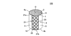
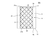
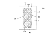
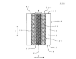
- FIG. 1 is a perspective view schematically showing an embodiment of a honeycomb structure of the present invention.
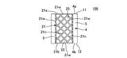
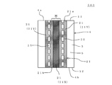
- 1 is a front view schematically showing one embodiment of a honeycomb structure of the present invention.
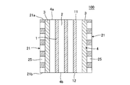
- 1 is a schematic diagram showing a cross section parallel to a cell extending direction of an embodiment of a honeycomb structure of the present invention.
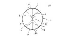
- FIG. 1 is a schematic diagram showing a cross section orthogonal to a cell extending direction of an embodiment of a honeycomb structure of the present invention. It is a front view which shows typically other embodiment of the honeycomb structure of this invention. It is a schematic diagram which expands and shows the area
- FIG. 6 is a front view schematically showing still another embodiment of the honeycomb structure of the present invention.
- FIG. 6 is a front view schematically showing still another embodiment of the honeycomb structure of the present invention.
- FIG. 6 is a front view schematically showing still another embodiment of the honeycomb structure of the present invention.
- FIG. 6 is a front view schematically showing still another embodiment of the honeycomb structure of the present invention.
- FIG. 6 is a front view schematically showing still another embodiment of the honeycomb structure of the present invention.
- FIG. 6 is a front view schematically showing still another embodiment of the honeycomb structure of the present invention.
- FIG. 6 is a front view schematically showing still another embodiment of the honeycomb structure of the present invention.
- FIG. 6 is a front view schematically showing still another embodiment of the honeycomb structure of the present invention.
- FIG. 6 is a front view schematically showing still another embodiment of the honeycomb structure of the present invention.
- FIG. 6 is a front view schematically showing still another embodiment of the honeycomb structure of the present invention.
- FIG. 6 is a front view schematically showing still another embodiment of the honeycomb structure of the present invention.
- FIG. 6 is a front view schematically showing still another embodiment of the honeycomb structure of
- FIG. 6 is a schematic view showing a cross section parallel to the cell extending direction of still another embodiment of the honeycomb structure of the present invention. It is a schematic diagram which shows a part of cross section orthogonal to the cell extending direction of other embodiment of the honeycomb structure of this invention.
- FIG. 6 is a front view schematically showing still another embodiment of the honeycomb structure of the present invention.
- FIG. 6 is a front view schematically showing still another embodiment of the honeycomb structure of the present invention.
- FIG. 6 is a schematic view showing a cross section perpendicular to the cell extending direction of still another embodiment of the honeycomb structure of the present invention.
- FIG. 6 is a front view schematically showing still another embodiment of the honeycomb structure of the present invention.
- FIG. 21 is a schematic diagram showing an A-A ′ cross section in FIG. 20.
- FIG. 6 is a side view schematically showing still another embodiment of the honeycomb structure of the present invention.
- FIG. 6 is a front view schematically showing still another embodiment of the honeycomb structure of the present invention.
- Honeycomb structure One embodiment of the honeycomb structure of the present invention is a tubular honeycomb structure having a porous partition wall 1 and an outer peripheral wall 3 located at the outermost periphery, as in the honeycomb structure 100 shown in FIGS. Part 4 and a pair of electrode parts 21, 21 arranged on side surface 5 of honeycomb structure part 4.
- the partition wall 1 partitions and forms a plurality of cells 2 "extending from one end surface 11 to the other end surface 12 serving as a fluid flow path".
- the honeycomb structure portion 4 has an electrical resistivity of 1 to 200 ⁇ cm.
- Each of the pair of electrode portions 21 and 21 of the honeycomb structure 100 is formed in a strip shape extending in the extending direction of the cells 2 of the honeycomb structure portion 4.
- FIG. 1 is a perspective view schematically showing one embodiment of a honeycomb structure of the present invention.
- FIG. 2 is a front view schematically showing one embodiment of the honeycomb structure of the present invention.
- FIG. 3 is a schematic view showing a cross section parallel to the cell extending direction of one embodiment of the honeycomb structure of the present invention.
- FIG. 4 is a schematic view showing a cross section perpendicular to the cell extending direction of one embodiment of the honeycomb structure of the present invention. In FIG. 4, the partition walls are omitted.
- the electrical resistivity of the honeycomb structure portion 4 is 10 to 200 ⁇ cm. Therefore, even if a current is supplied using a high voltage power source, the current does not flow excessively and can be suitably used as a heater.
- Each of the pair of electrode portions 21 and 21 is formed in a band shape, and one electrode portion 21 is disposed on the opposite side of the other electrode portion 21 with the center of the honeycomb structure portion 4 interposed therebetween. Yes. Therefore, it is possible to suppress an uneven temperature distribution of the honeycomb structure portion 4 when a voltage is applied between the pair of electrode portions 21 and 21.
- the honeycomb structure 100 has “the electrode portion 21 has a portion having a thickness of 0 to 70% of the maximum thickness of the electrode portion 21”, the rigidity of the electrode portion 21 and the outer peripheral wall 3 The difference from the rigidity becomes small.
- the pair of electrode portions 21 and 21 are electrodes for flowing a current through the honeycomb structure portion 4 (the partition wall 1 and the outer peripheral portion 3).
- the one electrode portion 21 in the pair of electrode portions 21, 21 is more than the other electrode portion 21 in the pair of electrode portions 21, 21.
- “Disposed on the opposite side across the center O” is defined as follows. In other words, in the cross section perpendicular to the extending direction of the cell 2, the positional relationship is such that the angle ⁇ formed by the line segment (A) and the line segment (B) is in the range of 170 ° to 190 °. This means that the pair of electrode portions 21 and 21 are disposed in the honeycomb structure portion 4.
- the line segment (A) is a line segment connecting the center point of one electrode portion 21 (the center point in the “circumferential direction of the honeycomb structure portion 4”) and the center O of the honeycomb structure portion 4.
- the line segment (B) is a line segment connecting the center point of the other electrode portion 21 (the center point in the “circumferential direction of the honeycomb structure portion 4”) and the center O of the honeycomb structure portion 4.
- the angle ⁇ is an angle centered on the “center O”.
- the material of the partition walls 1 and the outer peripheral wall 3 is preferably a silicon-silicon carbide composite material or a silicon carbide material as a main component, and a silicon-silicon carbide composite material or More preferably, it is a silicon carbide material.
- the material of the partition wall 1 and the outer peripheral wall 3 is mainly composed of a silicon-silicon carbide composite material or a silicon carbide material
- the partition wall 1 and the outer peripheral wall 3 are formed of a silicon-silicon carbide composite material or carbonized carbon. It means that 90% by mass or more of the silicon material is contained.
- the electrical resistivity of the honeycomb structure portion can be set to 10 to 200 ⁇ cm.
- the silicon-silicon carbide composite material contains silicon carbide particles as an aggregate and silicon as a binder for bonding the silicon carbide particles.
- the plurality of silicon carbide particles are preferably bonded by silicon so as to form pores between the silicon carbide particles.
- the silicon carbide material is obtained by sintering silicon carbide particles.
- the electrical resistivity of the honeycomb structure part is a value at 400 ° C.
- a pair of electrode portions 21 and 21 are disposed on the side surface 5 of the honeycomb structure portion 4.
- the honeycomb structure 100 of the present embodiment generates heat when a voltage is applied between the pair of electrode portions 21 and 21.
- the applied voltage is preferably 12 to 900V, and more preferably 64 to 600V.
- each of the pair of electrode portions 21 and 21 is formed in a strip shape extending in the extending direction of the cells 2 of the honeycomb structure portion 4.
- one electrode portion 21 in the pair of electrode portions 21, 21 has a honeycomb structure with respect to the other electrode portion 21 in the pair of electrode portions 21, 21. It is arranged on the opposite side across the central portion O of the portion 4.
- 0.5 times the central angle ⁇ is preferably 15 to 65 °, more preferably 20 to 65 °, and more preferably 30 to 60 °. Is particularly preferred.
- the central angle ⁇ is the central angle of each electrode portion 21, 21 in a cross section orthogonal to the extending direction of the cell 2.
- 0.5 times the central angle ⁇ means an angle ⁇ that is 0.5 times the central angle ⁇ .
- the center angle ⁇ of each electrode portion 21, 21 is 0.5.
- the double angle ⁇ is 15 to 65 °.
- the central angle ⁇ of the electrode portion 21 is two lines connecting the both ends of the electrode portion 21 and the center O of the honeycomb structure portion 4 in a cross section orthogonal to the extending direction of the cell 2.
- the angle formed by the minutes refers to the shape formed by the electrode part 21, the line segment (a), and the line segment (b) in the cross section orthogonal to the extending direction of the cell 2 (for example, , A sector shape) is an inner angle of the center O portion.
- the line segment (a) is a line segment connecting one end of the electrode portion 21 and the center O.
- the line segment (b) is a line segment connecting the other end of the electrode portion 21 and the center O.
- the “angle ⁇ that is 0.5 times the central angle ⁇ ” of the one electrode portion 21 is 0.8 ⁇
- the size is preferably 1.2 times, and more preferably 1.0 times the size (the same size).
- the electrode portion has a portion having a thickness of 0 to 70% of the maximum thickness of the electrode portion, and preferably has a portion having a thickness of at least 0%. That is, the electrode part preferably has a through hole.
- the electrode portion has the above-described portion, it is possible to suppress the generation of a large stress in the honeycomb structure portion even when there is rapid heating or rapid cooling when the honeycomb structure is mounted on an automobile and used. Therefore, the honeycomb structure of the present embodiment has excellent thermal shock resistance.
- the through hole of the electrode portion has a shape in which a corner portion is chamfered in a curved shape.
- the opening area can be 0.01 to 100 mm 2 .
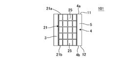
- FIG. 5 is a front view schematically showing another embodiment of the honeycomb structure of the present invention.
- FIG. 5 shows an example in which the shape of the opening of the through hole (thin portion 25) of the electrode portion 21 is a shape in which square corners are formed in a curved shape.
- the shape of the opening portion of the through hole 25 of the electrode portion 21 is such a shape, the opening portion is generated in the electrode portion 21 as compared with the case where the shape of the opening portion is a square with a corner portion (the corner portion is not curved). Stress is reduced.
- FIG. 6 is a schematic diagram showing the region P in FIG. 5 in an enlarged manner.
- a value (S / U) of the ratio of the area S to the area T and the total U of the areas S is preferably 0.1 to 0.8, and more preferably 0.2 to 0.7. preferable.
- the value of the ratio is in the above range, the rigidity of the electrode portion is lowered. Therefore, there is an advantage that the stress generated in the honeycomb structure is reduced.
- the value of the ratio is less than 0.1, the resistance of the electrode portion increases, so that when a voltage is applied, the effect of flowing a current more uniformly throughout the honeycomb structure portion is reduced (the effect is Not enough).
- the area S and the area T can be calculated by performing image processing on the surface of the electrode portion.
- the area S is an area of a portion that is 100% of the maximum thickness of the electrode portion (that is, the same thickness as the maximum thickness) in the plan view of the electrode portion.
- the area T is an area of a portion having a thickness of 0 to 70% of the maximum thickness.
- the “portion having a thickness of 0 to 70% of the maximum thickness of the electrode portion” can be defined as follows. That is, it means a portion (including a case where there is no thickness) where the thickness of the electrode portion is thinner than the maximum thickness of the electrode portion due to the formation of a space consisting of at least one of a through hole and a depression. .
- the outer peripheral shape, the formation position, etc. of the above part there is no particular limitation on the outer peripheral shape, the formation position, etc. of the above part as long as it has a part having a thickness of 0 to 70% of the maximum thickness.
- the outer peripheral shape of the portion having a thickness of 0 to 70% of the maximum thickness of the electrode portion is a triangle, a quadrangle, a circle, an ellipse, and a corner is curved (a corner is chamfered in a curved shape).
- a square etc. can be mentioned.
- a plurality of portions having a thickness of 0 to 70% of the maximum thickness of the electrode portion are provided, they may be formed so as to be aligned or irregularly formed.
- the electrode portion 21 of the honeycomb structure 100 shown in FIGS. 1 to 4 has a square-shaped through hole whose outer peripheral shape is a square “a portion having a thickness of 0 to 70% of the maximum thickness of the electrode portion”. This is an example in which they are formed in alignment. That is, the honeycomb structure 100 shown in FIGS. 1 to 4 is an example in which the net-like electrode portion 21 is formed. Note that the net-like electrode portion 21 may have a shape in which the outer peripheral portion is deleted. That is, the net-like electrode portion may be a net-like shape in which the outer peripheral edge portion 21w of the electrode portion 21 shown in FIG. 2 is not formed.
- the net-like electrode portion may be a net-like shape composed of a plurality of linear portions 21n formed to be inclined with respect to the cell extending direction of the honeycomb structure 100.
- the net-like electrode part 21 the part which is 100% of the maximum thickness of an electrode part may be formed vertically and horizontally like the honeycomb structure 101 shown in FIG.
- the net-like electrode portion 21 may be formed so as to be parallel to the cell extending direction of the honeycomb structure 101 and orthogonal to the cell extending direction of the honeycomb structure 101.
- FIG. 7 is a front view schematically showing another embodiment of the honeycomb structure of the present invention.
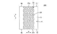
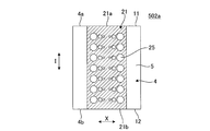
- the electrode portion 21 of the honeycomb structure 200 shown in FIG. 8 has a plurality of through-holes (thin portions 25) aligned in the cell I extending direction I of the honeycomb structure 200 and a plurality in the circumferential direction X.
- This is an example in which rows are formed.
- the honeycomb structure 200 shown in FIG. 8 is an example in which the electrode portion 21 having a shape like a so-called punching plate is formed.
- the through-hole is a through-hole having a circular outer peripheral shape “a portion having a thickness of 0 to 70% of the maximum thickness of the electrode portion”.
- FIG. 8 is a front view schematically showing another embodiment of the honeycomb structure of the present invention.
- the arrangement of the through holes (thin portions 25) is not particularly limited, and may be an arrangement in which the through holes are formed vertically and horizontally so as to be adjacent to each other as in the honeycomb structure 201 shown in FIG.
- FIG. 9 is a front view schematically showing another embodiment of the honeycomb structure of the present invention.
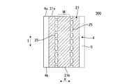
- the electrode portion 21 of the honeycomb structure 300 shown in FIG. 10 has a plurality of through-holes (thin portions 25) aligned in the cell I extending direction I of the honeycomb structure 300 and a plurality in the circumferential direction X. This is an example in which rows are formed.
- the above-mentioned through hole is an “peripheral portion having a thickness of 0 to 70% of the maximum thickness of the electrode portion” having an elliptical outer shape.
- a region M located at the center of the electrode portion 21 has a “portion having a thickness of 0 to 70% of the maximum thickness of the electrode portion”. This is an example that is not formed.
- FIG. 10 is a front view schematically showing still another embodiment of the honeycomb structure of the present invention.
- FIG. 11 is a front view schematically showing another embodiment of the honeycomb structure of the present invention.
- a honeycomb structure 301 shown in FIG. 11 is an example having an electrode part 21 in which a circular through hole (thin part 25) is formed instead of an elliptical through hole (thin part 25).
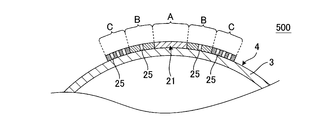
- part (a) which is “a part having a thickness of 0 to 70% of the maximum thickness of the electrode part” is formed. It is preferred that That is, the electrode portion has a plurality of regions, and in the cross section orthogonal to the cell extending direction, the “part (a)” is formed with a higher density from the region located in the center toward the region located outside. Is preferred.
- the “plurality of regions” are a plurality of regions in which the electrode portions 21 are arranged along the outer periphery of the honeycomb structure portion 4 in a cross section orthogonal to the cell extending direction. In other words, “a plurality of regions” in FIG.
- the 12 refers to a plurality of regions of region A in the electrode portion, region B in the electrode portion, and region C in the electrode portion. That is, it is preferable that the value (S / U) of the area S and the ratio of the area T and the total U of the areas S decreases from the central region to the outer region.
- the area S is an area of a portion that is 100% of the maximum thickness of the electrode portion (that is, the same thickness as the maximum thickness) in the plan view of the electrode portion.
- the area T is an area of a portion having a thickness of 0 to 70% of the maximum thickness.
- honeycomb structure having an electrode portion in which a “portion having a thickness of 0 to 70% of the maximum thickness of the electrode portion” is formed at a higher density from the central region to the outer region.
- honeycomb structures 501, 502a, and 502b shown in FIGS. 13, 14A, and 14B include honeycomb structures 501, 502a, and 502b shown in FIGS. 13, 14A, and 14B.
- a honeycomb structure 501 shown in FIG. 13 has a thickness of 0 to 70% of the maximum thickness of the electrode portion as it goes from the centrally located region to the outside region in the net-like electrode portion as shown in FIG. This is an example having an electrode portion formed with a high density.
- the honeycomb structures 502a and 502b shown in FIGS. 14A and 14B have electrode portions in which through holes (thin portions 25) having a larger opening area are formed from the region located in the center toward the region located outside. It is an example.
- the distance between the side edge side thin portion which is the thin portion located on the most side edge side of the electrode portion and the outer peripheral edge of the electrode portion is 0.5 to 1.. 5 mm is preferable. Further, in the honeycomb structure as shown in FIGS. 14A and 14B, the distance between the side edge side thin portion and the thin portion closest to the side edge side thin portion is preferably 0.5 to 2 mm. In the honeycomb structure as shown in FIGS. 14A and 14B, it is more preferable that a thin portion is not formed in a region located at the center of the electrode portion 21 in a cross section orthogonal to the cell extending direction.
- Thin part means “a part having a thickness of 0 to 70% of the maximum thickness of the electrode part”.
- the “honeycomb structure as shown in FIGS. 14A and 14B” has a “portion having a thickness of 0 to 70% of the maximum thickness of the electrode portion” from the region located in the center toward the region located outside.
- the “side edge” is an edge in the circumferential direction of the honeycomb structure portion.
- the distance D1 between the through hole (thin portion 25) located on the most side edge 13 side and the outer peripheral edge 15 of the electrode portion 21 is 1.0 mm. Further, the honeycomb structure 502b shown in FIG. 14B has a distance D2 between the through hole (side edge side thin portion 25a) located closest to the side edge 13 and the thin portion 25 closest to the side edge side thin portion 25a. It is 1.25 mm. Furthermore, in the honeycomb structure 502b shown in FIG. 14B, the thin portion 25 is not formed in the region M located in the center of the electrode portion 21.
- the honeycomb structure has cavities, and the total thickness excluding the cavities may be 0 to 70% of the maximum thickness of the electrode portion.
- the “cavity” is a cavity having a diameter of 100 ⁇ m or more inside the electrode portions 21 and 21 (hereinafter, simply referred to as “cavity”).
- the “thickness excluding the cavity” is the length excluding the portion occupied by the cavity from the thickness of the electrode part.
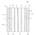
- a honeycomb structure 600 shown in FIG. 15 is an example in which a plurality of cavities 26 having a diameter of 100 ⁇ m or more are formed inside a pair of electrode portions 21 and 21.
- the shape and number of the cavities 26 are not particularly limited.
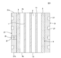
- a honeycomb structure 601 shown in FIG. 16 is an example in which a plurality of depressions 27 are formed on the surfaces of the pair of electrode portions 21 and 21. That is, the pair of electrode portions 21 and 21 of the honeycomb structure 601 shown in FIG. 16 is an example in which the hollow portion 25 is formed to have the thin portion 25.
- the recess 27 is not limited in the shape of the opening, and is an opening such as a triangle, a quadrangle, a hexagon, an octagon, a circle, an ellipse, or a polygon whose corner is curved (the corner is chamfered in a curved shape). It can be a part shape.
- the opening area can be 0.01 to 100 mm 2 .
- the thin portion need not have the same thickness throughout the electrode portion.
- the electrode portion in the cross section orthogonal to the cell extending direction, is formed such that the region located at the center is thickest and the region located outside is thinned, and the regions located at both ends are thinnest. Preferably it is formed.
- a honeycomb structure 500 shown in FIG. 12 has a plurality of regions in which the electrode portion 21 is arranged along the outer periphery of the honeycomb structure portion 4 in a cross section orthogonal to the cell extending direction.
- the “plurality of regions” refers to a plurality of regions including a region A in the electrode part, a region B in the electrode part, and a region C in the electrode part.
- the region located outside the electrode portion is formed thinner so that the bias of the temperature distribution in the honeycomb structure portion is further reduced when a voltage is applied to the electrode portion. can do.
- the electrode part has a plurality of regions, the number of the regions is not particularly limited, and is preferably about 2 to 4.
- the electrode portion may have a smooth shape with “continuously changing thickness” without a step in a cross section perpendicular to the cell extending direction.
- the electrode portion is formed in a strip shape extending in the cell extending direction of the honeycomb structure portion.
- a pair of electrode portions 21, 21 may be formed between both end portions of the honeycomb structure portion 4 (from one end portion 4 a to the other end portion 4 b).
- the pair of electrode portions 21 and 21 may be formed so that one end portion 21a and the other end portion 21b are aligned with the one end portion 4a and the other end portion 4b of the honeycomb structure portion 4, respectively. Good.
- the “one end portion 4a” and the “one end portion 21a of the electrode portion 21” are separated from each other, and the “other end portion 4b” and the “electrode portion 21” are separated. May be separated from the other end portion 21b ".
- One end 4a is one end 4a of the honeycomb structure 4 in the cell 2 extending direction.
- the other end 4b is the other end 4b of the honeycomb structure 4 in the cell 2 extending direction.
- the electrode part 21 is formed from one end part 4a to the other end part 4b of the honeycomb structure part 4 in a cross section parallel to the cell 2 extending direction. This is because when the electrode portion is formed in this way, the honeycomb structure 4 can be uniformly heated when a voltage is applied to the honeycomb structure 4.
- the outer peripheral shape of the belt-like electrode portion can be a shape in which at least one corner of the rectangle is formed in a curved shape, or a shape in which at least one corner of the rectangle is chamfered in a straight line.
- the thermal shock resistance of the honeycomb structure can be further improved when the shape is such that at least one corner of the rectangle is formed in a curved shape.
- the corner portion of the electrode portion is a right angle, the stress near the “corner portion of the electrode portion” in the honeycomb structure portion tends to be relatively high as compared with other portions.
- the corners of the electrode portions are curved, the stress near the “corner portions of the electrode portions” in the honeycomb structure portion can be further reduced.
- the corners formed in a curved shape are preferably arcuate.
- the outer peripheral shape of the electrode portion 21 is a shape in which at least one corner portion of the rectangle is formed in a curved shape” Effects similar to those obtained sometimes can be obtained. A higher effect can be obtained when the corners are curved.
- the “strip shape” in this specification can be referred to as a sheet shape or a film shape. That is, the “electrode part” in the present specification does not include the one that protrudes outward like the “electrode terminal protrusion” in the present specification.
- the maximum thickness of the electrode portion is preferably 0.025 to 3 mm, more preferably 0.025 to 0.7 mm, and 0.05 to 0.5 mm. It is particularly preferred. By setting it within such a range, heat can be generated uniformly.
- the maximum thickness of the electrode part is less than 0.025 mm, the resistance of the electrode part increases, so that when a voltage is applied, the effect of flowing a current more uniformly throughout the honeycomb structure part (ie, uniform The effect of causing heat generation) may be reduced.
- it exceeds 3 mm the honeycomb structure may be damaged during canning.
- the thickness of the outer peripheral wall 3 constituting the outermost periphery of the honeycomb structure portion 4 is preferably 0.1 to 1 mm, more preferably 0.2 to 0.8 mm, and more preferably 0.2 to 0.5 mm. It is particularly preferred that If it is thinner than 0.1 mm, the strength of the honeycomb structure 100 (honeycomb structure portion 4) may be lowered. If it is thicker than 1 mm, the area of the partition wall supporting the catalyst may be small.
- the total heat capacity of the pair of electrode portions is preferably 2 to 150% of the heat capacity of the entire outer peripheral wall.
- the total heat capacity of the pair of electrode portions is more preferably less than or equal to the heat capacity of the entire outer peripheral wall (that is, 2 to 100%), and particularly preferably smaller than the heat capacity of the entire outer peripheral wall.
- the sum of the heat capacities of the pair of electrode portions is a value derived by a heat capacity calculation method that takes into account the porosity, the specific gravity of the material, and the specific heat based on the volume of the electrode portions.
- the “volume of the electrode part” refers to the volume of the electrode part calculated using the average thickness of the electrode part and the electrode angle (center angle ⁇ in FIG. 4) measured with an optical microscope.
- the heat capacity of the entire outer peripheral wall is a value derived by a heat capacity calculation method that takes into account the porosity, the specific gravity of the material, and the specific heat based on the volume of the outer peripheral wall.
- the “volume of the outer peripheral wall” refers to the volume of the outer peripheral wall calculated using the average thickness of the outer peripheral wall measured with an optical microscope.
- contact area of the electrode portion the area of the portion where the electrode portion is in contact with the side surface of the honeycomb structure portion.
- a cylinder that is coaxial with the honeycomb structure part and divides the electrode part is assumed, and a divided surface of the electrode part divided into the cylinder is defined as a virtual divided surface.
- the area of this virtual division plane is referred to as “virtual division area”.
- the “virtual division” is used in the calculation of the “heat capacity of the electrode portion” in the present specification.
- a portion where the “area” is 90% or more of the “contact area of the electrode portion” is referred to as an “electrode portion”. That is, in the above case, when calculating the “heat capacity of the electrode part” in this specification, the part where the “virtual divided area” is less than 90% of the “contact area of the electrode part” is not an electrode part.
- the total heat capacity of the pair of electrode portions is smaller than the heat capacity of the entire outer peripheral wall
- the total heat capacity of the pair of electrode portions is the entire outer wall. It is preferably 2 to 80% of the heat capacity.
- the lower limit is more preferably 9%, and particularly preferably 15%.
- the upper limit value is more preferably 75%, and particularly preferably 50%. If it is less than 2%, the effect of “more uniformly flowing the current through the entire honeycomb structure when a voltage is applied” may be reduced. If it exceeds 80%, the effect of reducing the thermal shock resistance may be reduced.
- the electrical resistivity of the electrode portion 21 may be uniform or may be partially different.
- the electrical resistivity of the electrode portion 21 is preferably 0.01 to 100 ⁇ cm, more preferably 0.1 to 100 ⁇ cm, and more preferably 0.1 to 50 ⁇ cm. It is particularly preferred that By setting the electrical resistivity of the electrode portion 21 in such a range, the pair of electrode portions 21 and 21 effectively serve as electrodes in the pipe through which the high-temperature exhaust gas flows.
- the electrical resistivity of the electrode part 21 is smaller than 0.01 ⁇ cm, the temperature of the honeycomb structure part near both ends of the electrode part 21 may easily rise in a cross section orthogonal to the cell extending direction. If the electrical resistivity of the electrode portion 21 is larger than 100 ⁇ cm, it may be difficult to play a role as an electrode because current hardly flows.
- the electrical resistivity of the electrode part is a value at 400 ° C.
- the electrode part 21 is composed of a central part 21X and expansion parts 21Y and 21Y as in the honeycomb structure 503 shown in FIGS. It is preferable that the electrical resistivity of the central portion 21X of the 21 is smaller than the electrical resistivity of the extended portions 21Y and 21Y of the electrode portion 21.
- the central portion 21 ⁇ / b> X is a portion in the circumferential direction of the electrode portion 21 in a cross section orthogonal to the extending direction of the cell 2.
- the extended portions 21Y and 21Y are portions located on both sides in the circumferential direction of the central portion 21X in a cross section orthogonal to the extending direction of the cells 2.
- FIG. 18 is a front view schematically showing another embodiment of the honeycomb structure of the present invention.
- FIG. 19 is a schematic view showing a cross section orthogonal to the cell extending direction of another embodiment of the honeycomb structure of the present invention.
- the electrical resistivity of the central portion 21X is preferably 0.0001 to 70%, more preferably 0.001 to 50%, and particularly preferably 0.001 to 10% of the electrical resistivity of the extended portions 21Y and 21Y. If it is less than 0.0001%, the flow of current in the outer peripheral direction in the cross section perpendicular to the central axis of the honeycomb structure portion becomes small, and the deviation in temperature distribution may become large. If it is larger than 70%, the effect of suppressing the temperature distribution of the honeycomb structure 503 may be reduced.
- the Young's modulus of the electrode portion 21 is preferably 2 to 50 GPa, more preferably 3 to 45 GPa, and particularly preferably 3 to 35 GPa.
- the Young's modulus of the electrode part 21 is preferably 2 to 50 GPa, more preferably 3 to 45 GPa, and particularly preferably 3 to 35 GPa.
- the Young's modulus may be uniform within the electrode portion 21 or may be partially different. When the Young's modulus is partially different, the above effect can be obtained if a part is within the above range, and the above effect is further enhanced if all are within the above range.
- the Young's modulus of the electrode part is a value measured by a bending resonance method in accordance with JIS R1602. As a test piece used for measurement, after a plurality of sheets made of electrode part forming raw materials for forming an electrode part were stacked to obtain a laminate, the laminate was dried and cut into a size of 3 mm ⁇ 4 mm ⁇ 40 mm. Use things.
- the electrode portion 21 is preferably composed mainly of silicon carbide particles and silicon, and more preferably formed from silicon carbide particles and silicon as raw materials other than impurities that are usually contained.
- “mainly composed of silicon carbide particles and silicon” means that the total mass of the silicon carbide particles and silicon is 90% by mass or more of the mass of the entire electrode portion.
- the electrode part 21 is composed mainly of silicon carbide particles and silicon, so that the component of the electrode part 21 and the component of the honeycomb structure part 4 are the same component or It becomes a close ingredient. That is, the thermal expansion coefficients of the electrode portion 21 and the honeycomb structure portion 4 are the same value or close values.
- the bonding strength between the electrode portion 21 and the honeycomb structure portion 4 is also increased. Therefore, even when thermal stress is applied to the honeycomb structure, it is possible to prevent the electrode portion 21 from being peeled off from the honeycomb structure portion 4 and the joint portion between the electrode portion 21 and the honeycomb structure portion 4 being damaged.
- the electrode part 21 preferably has a porosity of 30 to 80%, more preferably 30 to 70%.
- a porosity of the electrode portion 21 is in such a range, a suitable electrical resistivity can be obtained. If the porosity of the electrode portion 21 is lower than 30%, it may be deformed during manufacturing. When the porosity of the electrode part 21 is higher than 80%, the electrical resistivity may become too high.
- the porosity is a value measured with a mercury porosimeter.
- the electrode part 21 preferably has an average pore diameter of 5 to 45 ⁇ m, more preferably 7 to 40 ⁇ m.
- the average pore diameter of the electrode part 21 is in such a range, a suitable electrical resistivity can be obtained.
- the average pore diameter of the electrode part 21 is smaller than 5 ⁇ m, the electrical resistivity may become too high.
- the average pore diameter of the electrode part 21 is larger than 40 ⁇ m, the strength of the electrode part 21 is weakened and may be easily damaged.
- the average pore diameter is a value measured with a mercury porosimeter.
- the average particle diameter of the silicon carbide particles contained in the electrode part 21 is preferably 10 to 70 ⁇ m, and more preferably 10 to 60 ⁇ m.
- the electrical resistivity of the electrode portion 21 can be controlled in the range of 0.1 to 100 ⁇ cm. If the average pore diameter of the silicon carbide particles contained in the electrode portion 21 is smaller than 10 ⁇ m, the electrical resistivity of the electrode portion 21 may become too large. When the average pore diameter of the silicon carbide particles contained in the electrode portion 21 is larger than 70 ⁇ m, the strength of the electrode portion 21 is weakened and may be easily damaged.
- the average particle diameter of the silicon carbide particles contained in the electrode part 21 is a value measured by a laser diffraction method.
- the ratio of the mass of silicon contained in the electrode part 21 is preferably 20 to 50% by mass, and more preferably 20 to 40% by mass. "The ratio of the mass of silicon contained in the electrode part 21" is the ratio of the mass of silicon contained in the electrode part 21 to the "total of the respective masses of silicon carbide particles and silicon" contained in the electrode part 21. That is.
- the electrical resistivity of the electrode portion 21 can be controlled in the range of 0.1 to 100 ⁇ cm. If the “ratio of the mass of silicon contained in the electrode portion 21” is less than 20% by mass, the electrical resistivity may be too high. On the other hand, if the “ratio of the mass of silicon contained in the electrode portion 21” is greater than 50 mass%, the electrode portion may be easily deformed during manufacturing.
- the partition wall thickness is 50 to 260 ⁇ m, and preferably 70 to 180 ⁇ m.
- the partition wall thickness is less than 50 ⁇ m, the strength of the honeycomb structure may be lowered.
- the partition wall thickness is larger than 260 ⁇ m, the pressure loss may increase when exhaust gas is flowed after the catalyst is supported on the honeycomb structure 100 as the catalyst carrier.
- the honeycomb structure 100 of the present embodiment preferably has a cell density of 40 to 150 cells / cm 2 , and more preferably 70 to 100 cells / cm 2 .
- the purification performance of the catalyst can be enhanced while reducing the pressure loss when the exhaust gas is flowed.
- the cell density is lower than 40 cells / cm 2
- the catalyst supporting area may be reduced.
- pressure loss may increase when exhaust gas is flowed after the catalyst is supported on the honeycomb structure 100 as the catalyst carrier.
- the average particle diameter of the silicon carbide particles (aggregate) constituting the honeycomb structure portion 4 is preferably 3 to 50 ⁇ m, and more preferably 3 to 40 ⁇ m.
- the electrical resistivity at 400 ° C. of the honeycomb structure part 4 can be 10 to 200 ⁇ cm.
- the electrical resistivity of the honeycomb structure portion 4 may be increased.
- the electrical resistivity of the honeycomb structure portion 4 may be reduced.
- the extrusion forming die may be clogged with the forming raw material when the honeycomb formed body is extruded.
- the average particle diameter of the silicon carbide particles is a value measured by a laser diffraction method.
- the electrical resistivity of the honeycomb structure portion 4 is 10 to 200 ⁇ cm, and preferably 40 to 100 ⁇ cm. If the electrical resistivity is less than 10 ⁇ cm, for example, an excessive current may flow when the honeycomb structure 100 is energized by a high-voltage power source of 200 V or higher.
- the voltage is not limited to 200V. If the electrical resistivity is greater than 200 ⁇ cm, for example, when the honeycomb structure 100 is energized by a high-voltage power supply of 200 V or more, it becomes difficult for current to flow, and heat generation may not occur sufficiently.
- the voltage is not limited to 200V.
- the electrical resistivity of the honeycomb structure part is a value measured by a four-terminal method.
- the electrical resistivity of the honeycomb structure part is a value at 400 ° C.
- the electrical resistivity of the electrode portion 21 is lower than the electrical resistivity of the honeycomb structure portion 4.
- the electrical resistivity of the electrode part 21 is preferably 20% or less of the electrical resistivity of the honeycomb structure part 4, and more preferably 1 to 10%.
- the “mass of silicon carbide particles” and the “mass of silicon” have the following relationship: Is preferred. That is, the ratio of “mass of silicon” to the total of “mass of silicon carbide particles” and “mass of silicon” is preferably 10 to 40% by mass, and more preferably 15 to 35% by mass. preferable. If it is lower than 10% by mass, the strength of the honeycomb structure may be lowered. If it is higher than 40% by mass, the shape may not be maintained during firing.
- the above “mass of silicon carbide particles” refers to “mass of silicon carbide particles as an aggregate” contained in the honeycomb structure portion 4.
- the above “mass of silicon” refers to “mass of silicon as a binder” contained in the honeycomb structure 4.
- the porosity of the partition walls 1 of the honeycomb structure portion 4 is preferably 35 to 60%, and more preferably 45 to 55%. If the porosity is less than 35%, deformation during firing may increase. When the porosity exceeds 60%, the strength of the honeycomb structure may be lowered.
- the porosity is a value measured with a mercury porosimeter.
- the average pore diameter of the partition walls 1 of the honeycomb structure part 4 is preferably 2 to 15 ⁇ m, and more preferably 4 to 8 ⁇ m. If the average pore diameter is smaller than 2 ⁇ m, the electrical resistivity may become too large. If the average pore diameter is larger than 15 ⁇ m, the electrical resistivity may be too small.
- the average pore diameter is a value measured with a mercury porosimeter.
- the shape of the cell 2 in a cross section perpendicular to the extending direction of the cell 2 is a quadrangle, a hexagon, an octagon, or a combination thereof.
- the shape of the honeycomb structure 100 of the present embodiment is not particularly limited.
- the bottom surface may have a circular cylindrical shape (cylindrical shape), the bottom surface may have an oval cylindrical shape, and the bottom surface may have a polygonal shape (square, pentagon, hexagon, heptagon, octagon, etc.). it can.
- the honeycomb structure has a bottom surface area of preferably 2000 to 20000 mm 2 , and more preferably 4000 to 10000 mm 2 .
- the length of the honeycomb structure in the central axis direction is preferably 50 to 200 mm, and more preferably 75 to 150 mm.
- the isostatic strength of the honeycomb structure 100 of the present embodiment is preferably 1 MPa or more, and more preferably 3 MPa or more. The larger the value of isostatic strength, the better. Considering the material and structure of the honeycomb structure 100, the upper limit is about 6 MPa. When the isostatic strength is less than 1 MPa, the honeycomb structure may be easily damaged when used as a catalyst carrier or the like. Isostatic strength is a value measured by applying hydrostatic pressure in water.
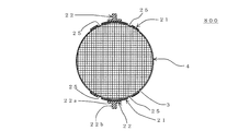
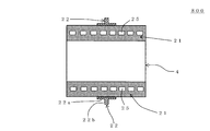
- the honeycomb structure 800 of the present embodiment is provided with the electrode terminal protrusions 22 for connecting the electrical wirings in the honeycomb structure 300 of the embodiment (see FIG. 10). It has been done.
- the electrode terminal protrusion 22 is the central portion of each electrode portion 21, 21 in the cross section orthogonal to the cell extending direction, and is disposed in the central portion in the cell extending direction. . “The central portion in the cross section perpendicular to the cell extending direction” refers to the central portion in the circumferential direction of the honeycomb structure portion.
- the electrode terminal protrusion 22 is a portion for connecting a wiring from a power source in order to apply a voltage between the electrode portions 21 and 21.
- FIG. 20 is a front view schematically showing still another embodiment of the honeycomb structure of the present invention.
- FIG. 21 is a schematic diagram showing the AA ′ cross section in FIG.
- FIG. 22 is a side view schematically showing still another embodiment of the honeycomb structure of the present invention.
- Each condition of the honeycomb structure 800 of the present embodiment is the same as each condition in still another embodiment (the honeycomb structure 300 (see FIG. 10)) of the honeycomb structure of the present invention, except for the following condition (X).
- the condition (X) is “the center part of each electrode part 21, 21 in the cross section perpendicular to the extending direction of the cell 2, and the electrode for connecting the electric wiring to the central part in the extending direction of the cell 2.
- the terminal protrusion 22 is disposed ”.
- an electrode portion 21 as shown in FIG. 20 is provided. That is, the electrode portion 21 shown in FIG. 20 has a cross section perpendicular to the cell extending direction in a region M where “a portion having a thickness of 0 to 70% of the maximum thickness of the electrode portion” is located at the center. It is not formed, but is formed in a region other than the region M located at the center. In such a case, the electrode terminal protrusion 22 is easily disposed in the “region M located in the center” where the “portion having a thickness of 0 to 70% of the maximum thickness of the electrode portion” is not formed. Can do.
- the main components of the electrode terminal protrusion 22 are also preferably silicon carbide particles and silicon.
- the electrode terminal protrusion 22 has silicon carbide particles and silicon as main components, the component of the electrode part 21 and the component of the electrode terminal protrusion 22 are the same (or close) components. Therefore, the thermal expansion coefficient of the electrode part 21 and the electrode terminal protrusion part 22 becomes the same (or close) value. Further, since the materials are the same (or close), the bonding strength between the electrode portion 21 and the electrode terminal protrusion 22 is increased.
- the electrode terminal protrusion 22 when “the electrode terminal protrusion 22 is composed mainly of silicon carbide particles and silicon”, the electrode terminal protrusion 22 contains 90% by mass or more of silicon carbide particles and silicon. Means that.
- the shape of the electrode terminal protrusion 22 is not particularly limited as long as it can be bonded to the electrode 21 and can be connected to the electric wiring.
- the electrode terminal protrusion 22 preferably has a shape in which a cylindrical protrusion 22b is disposed on a rectangular plate-shaped substrate 22a. With this shape, the electrode terminal protrusion 22 can be firmly bonded to the electrode portion 21 by the substrate 22a. Then, the electrical wiring can be reliably bonded by the protrusion 22b.
- the thickness of the substrate 22a is preferably 1 to 5 mm. By setting it as such thickness, the electrode terminal protrusion part 22 can be joined to the electrode part 21 reliably. If the thickness is less than 1 mm, the substrate 22a becomes weak, and the protrusion 22b may be easily detached from the substrate 22a. If it is thicker than 5 mm, the space for arranging the honeycomb structure may become larger than necessary.
- the length (width) of the substrate 22 a is preferably 10 to 50%, more preferably 20 to 40% of the length of the electrode portion 21. By setting it as such a range, the electrode terminal protrusion part 22 becomes difficult to remove
- the “length (width) of the substrate 22a” is the length of the substrate 22a in the “peripheral direction in the cross section perpendicular to the cell extending direction of the honeycomb structure portion 4”.
- the “length of the electrode part 21” is the length of the electrode part 21 in “the outer peripheral direction (direction along the outer periphery) in the cross section of the honeycomb structure part 4 orthogonal to the cell extending direction”.
- the length of the substrate 22a in the “cell 2 extending direction” is preferably 5 to 30% of the length of the honeycomb structure 4 in the cell extending direction. By setting the length of the substrate 22a in the “direction in which the cells 2 extend” within such a range, sufficient bonding strength can be obtained. If the length of the substrate 22 a in the “cell 2 extending direction” is shorter than 5% of the length of the honeycomb structure portion 4 in the cell extending direction, the substrate 22 a may be easily detached from the electrode portion 21. And if it is longer than 30%, the mass may increase.
- the thickness of the protrusion 22b is preferably 3 to 15 mm. With such a thickness, the electrical wiring can be reliably bonded to the protrusion 22b. If it is thinner than 3 mm, the protrusion 22b may be easily broken. If it is thicker than 15 mm, it may be difficult to connect the electrical wiring.
- the length of the protrusion 22b is preferably 3 to 20 mm. With such a length, the electrical wiring can be reliably bonded to the protrusion 22b. If it is shorter than 3 mm, it may be difficult to join the electric wiring. If it is longer than 20 mm, the protrusion 22b may be easily broken.
- the electrical resistivity of the electrode terminal protrusion 22 is preferably 0.1 to 2.0 ⁇ cm, and more preferably 0.1 to 1.0 ⁇ cm. By setting the electrical resistivity of the electrode terminal protrusion 22 in such a range, current can be efficiently supplied from the electrode terminal protrusion 22 to the electrode portion 21 in the pipe through which high-temperature exhaust gas flows. If the electrical resistivity of the electrode terminal protrusion 22 is greater than 2.0 ⁇ cm, it may be difficult to supply current to the electrode portion 21 because current does not flow easily.
- the electrode terminal protrusion 22 preferably has a porosity of 30 to 45%, and more preferably 30 to 40%. When the porosity of the electrode terminal protrusion 22 is within such a range, an appropriate electrical resistivity can be obtained. If the porosity of the electrode terminal protrusion 22 is higher than 45%, the strength of the electrode terminal protrusion 22 may be reduced. In particular, when the strength of the protrusion 22b of the electrode terminal protrusion 22 is lowered, the protrusion 22b may be easily broken.
- the porosity is a value measured with a mercury porosimeter.
- the electrode terminal protrusion 22 preferably has an average pore diameter of 5 to 20 ⁇ m, and more preferably 7 to 15 ⁇ m. When the average pore diameter of the electrode terminal protrusion 22 is within such a range, an appropriate electrical resistivity can be obtained. If the average pore diameter of the electrode terminal protrusion 22 is larger than 20 ⁇ m, the strength of the electrode terminal protrusion 22 may be reduced. In particular, when the strength of the protrusion 22b of the electrode terminal protrusion 22 is lowered, the protrusion 22b may be easily broken.
- the average pore diameter is a value measured with a mercury porosimeter.
- the average particle diameter of the silicon carbide particles contained in the electrode terminal protrusion 22 is preferably 10 to 60 ⁇ m, and preferably 20 to 60 ⁇ m. More preferably.
- the electrical resistivity of the electrode terminal protrusion 22 can be set to 0.1 to 2.0 ⁇ cm. If the average pore diameter of the silicon carbide particles contained in the electrode terminal protrusion 22 is smaller than 10 ⁇ m, the electrical resistivity of the electrode terminal protrusion 22 may become too large.
- the average particle diameter of the silicon carbide particles contained in the electrode terminal protrusion 22 is a value measured by a laser diffraction method.
- the ratio of the mass of silicon contained in the electrode terminal protrusion 22 is preferably 20 to 40% by mass, and more preferably 25 to 35% by mass.
- the “ratio of the mass of silicon contained in the electrode terminal protrusion 22” is contained in the electrode terminal protrusion 22 with respect to the “total of the respective masses of silicon carbide particles and silicon” contained in the electrode terminal protrusion 22. This is the ratio of the mass of silicon.
- the ratio of the mass of silicon contained in the electrode terminal protrusion 22 is within such a range, it becomes easy to obtain an electrical resistivity of 0.1 to 2.0 ⁇ cm. If the ratio of the mass of silicon contained in the electrode terminal protrusion 22 is smaller than 20% by mass, the electrical resistivity may become too large. And when larger than 40 mass%, an electrode terminal protrusion part may deform
- honeycomb structure 900 of the present embodiment has an electric power lower than the electric resistivity of the electrode portion 21 in the above-described further embodiment (honeycomb structure 300) of the honeycomb structure of the present invention shown in FIG.
- a conductor 23 having resistivity is disposed on the surface of the electrode portion 21.
- the honeycomb structure 900 has the electrode portion 21 as shown in FIG. 23 and the conductor 23 disposed in a region M located in the center.
- the electrode portion 21 has a “portion having a thickness of 0 to 70% of the maximum thickness of the electrode portion” not formed in the central region M but in the center.
- FIG. 23 is a front view schematically showing still another embodiment of the honeycomb structure of the present invention.
- the conductor 23 having an electrical resistivity lower than that of the electrode portion 21 is installed on the surface of the electrode portion 21. Therefore, by applying a voltage to the conductor 23, it becomes possible to flow a current more uniformly through the entire honeycomb structure portion.
- the electrical resistivity of the conductor 23 is preferably 0.0001 to 70%, more preferably 0.001 to 50%, and particularly preferably 0.001 to 10% of the electrical resistivity of the electrode portion 21. If it is less than 0.0001%, the flow of current in the outer peripheral direction in the cross section perpendicular to the central axis of the honeycomb structure portion becomes small, and the deviation in temperature distribution may become large. If it is larger than 70%, the effect of suppressing the uneven temperature distribution of the honeycomb structure 900 may be lowered.
- the electrical resistivity is a value at 400 ° C.
- the shape of the conductor 23 is not particularly limited. As shown in FIG. 23, a rectangular shape that extends from one end 21a of the electrode portion to the other end 21b of the electrode portion is preferable. In addition, the conductor 23 does not need to span between the both ends of an electrode part. That is, there may be a gap between the end portion of the conductor 23 and the end portion of the electrode portion.
- the length of the conductor 23 is preferably 50% or more of the length of the electrode portion 21, more preferably 80% or more, and particularly preferably 100%. If it is shorter than 50%, when a voltage is applied, the effect of allowing a current to flow more uniformly through the entire honeycomb structure may be reduced.
- the “length of the conductor 23” is the length in the extending direction of the “cells of the honeycomb structure portion”.
- the “length of the electrode portion 21” is the length in the extending direction of the “cells of the honeycomb structure portion”.
- the length of the conductor 23 in the circumferential direction is not particularly limited as long as it is equal to or shorter than the length in the circumferential direction of the electrode portion.
- the circumferential length of the conductor 23 is preferably 5 to 75%, more preferably 10 to 60% of the circumferential length of the electrode portion. If it is longer than 75%, the temperature of the honeycomb structure near the both ends of the electrode portion 21 may easily rise in the cross section orthogonal to the cell extending direction. If it is shorter than 5%, when a voltage is applied, the effect of flowing a current more uniformly over the entire honeycomb structure portion may be reduced (cannot be sufficiently obtained).
- Examples of the material of the conductor 23 include a silicon carbide structure that is impregnated with silicon and has a porosity of 5% or less.
- the thickness of the conductor 23 is preferably 0.1 to 2 mm, more preferably 0.2 to 1.5 mm, and particularly preferably 0.3 to 1 mm. If it is thicker than 2 mm, the thermal shock resistance of the honeycomb structure may be lowered. If it is thinner than 0.1 mm, the strength of the conductor 23 may be reduced.
- honeycomb structure of the present embodiment can be used as a catalyst carrier.
- the honeycomb structure can be used as a catalyst for exhaust gas treatment.
- FIGS. 20 to 22 A method for manufacturing a honeycomb structure 800 (see FIGS. 20 to 22), which is still another embodiment of the above-described honeycomb structure of the present invention (hereinafter, may be referred to as “manufacturing method (A)”) is shown. .
- a forming raw material is prepared by adding metal silicon powder (metal silicon), a binder, a surfactant, a pore former, water, and the like to silicon carbide powder (silicon carbide). It is preferable that the mass of the metal silicon is 10 to 40% by mass with respect to the total of the mass of the silicon carbide powder and the mass of the metal silicon.
- the average particle diameter of the silicon carbide particles in the silicon carbide powder is preferably 3 to 50 ⁇ m, and more preferably 5 to 20 ⁇ m.
- the average particle diameter of metal silicon (metal silicon powder) is preferably 2 to 35 ⁇ m.
- the average particle diameter of silicon carbide particles and metal silicon (metal silicon particles) is a value measured by a laser diffraction method.
- Silicon carbide particles are fine particles of silicon carbide constituting silicon carbide powder.
- the metal silicon particles are fine particles of metal silicon constituting the metal silicon powder. This is a composition of a forming raw material when the material of the honeycomb structure part is a silicon-silicon carbide composite material. When the material of the honeycomb structure is silicon carbide, no metallic silicon is added.
- binder examples include methyl cellulose, hydroxypropyl methyl cellulose, hydroxypropoxyl cellulose, hydroxyethyl cellulose, carboxymethyl cellulose, and polyvinyl alcohol. Among these, it is preferable to use methyl cellulose and hydroxypropoxyl cellulose in combination.
- the content of the binder is preferably 2.0 to 10.0 parts by mass when the total mass of the silicon carbide powder and the metal silicon powder is 100 parts by mass.
- the water content is preferably 20 to 60 parts by mass when the total mass of the silicon carbide powder and the metal silicon powder is 100 parts by mass.
- ethylene glycol, dextrin, fatty acid soap, polyalcohol or the like can be used as the surfactant. These may be used individually by 1 type and may be used in combination of 2 or more type.
- the content of the surfactant is preferably 0.1 to 2.0 parts by mass when the total mass of the silicon carbide powder and the metal silicon powder is 100 parts by mass.
- the pore former is not particularly limited as long as it becomes pores after firing, and examples thereof include graphite, starch, foamed resin, water absorbent resin, silica gel and the like.
- the pore former content is preferably 0.5 to 10.0 parts by mass when the total mass of the silicon carbide powder and the metal silicon powder is 100 parts by mass.
- the average particle size of the pore former is preferably 10 to 30 ⁇ m. If it is smaller than 10 ⁇ m, pores may not be formed sufficiently. If it is larger than 30 ⁇ m, the die may be clogged during molding.
- the average particle diameter of the pore former is a value measured by a laser diffraction method.
- the forming raw material is kneaded to form a clay.
- molding raw material and forming a clay For example, the method of using a kneader, a vacuum clay kneader, etc. can be mentioned.
- the clay is extruded to form a honeycomb formed body.
- a die having a desired overall shape, cell shape, partition wall thickness, cell density and the like.
- a cemented carbide which does not easily wear is preferable.
- the honeycomb formed body has a structure having partition walls that form a plurality of cells that serve as fluid flow paths and an outer peripheral wall that is positioned on the outermost periphery.
- the partition wall thickness, cell density, outer peripheral wall thickness, etc. of the honeycomb molded body can be appropriately determined in accordance with the structure of the honeycomb structure of the present invention to be manufactured in consideration of shrinkage during drying and firing.
- the drying method is not particularly limited, and examples thereof include an electromagnetic heating method such as microwave heating drying and high-frequency dielectric heating drying, and an external heating method such as hot air drying and superheated steam drying. Among these, it is preferable to dry a certain amount of moisture by an electromagnetic heating method and then dry the remaining moisture by an external heating method. This is because the entire molded body can be dried quickly and uniformly without cracks. As drying conditions, it is preferable to remove 30 to 99% by mass of water with respect to the amount of moisture before drying by an electromagnetic heating method, and then to make the moisture to 3% by mass or less by an external heating method. . As the electromagnetic wave heating method, dielectric heating drying is preferable. As an external heating method, hot air drying is preferable.
- the length in the central axis direction of the honeycomb formed body is not a desired length, it is preferable to cut both end surfaces (both end portions) to a desired length.
- the cutting method is not particularly limited, and examples thereof include a method using a circular saw cutter.
- an electrode part forming raw material for forming the electrode part is prepared.
- the electrode part forming raw material is preferably prepared by adding a predetermined additive to silicon carbide powder and silicon powder and kneading.
- a center part formation raw material and an expansion part formation raw material are each prepared.
- the central part forming raw material is preferably formed by adding predetermined additives to the silicon carbide powder and silicon powder and kneading.
- the extended portion forming raw material is preferably formed by adding a predetermined additive to the silicon carbide powder and the silicon powder and kneading.
- metal silicon powder metal silicon
- a binder a surfactant, a pore former, water, and the like are added to silicon carbide powder (silicon carbide) and kneaded to prepare an electrode part forming raw material.
- silicon carbide powder silicon carbide
- the mass of metal silicon is preferably 20 to 40 parts by mass.
- the average particle diameter of the silicon carbide particles in the silicon carbide powder is preferably 10 to 60 ⁇ m.
- the average particle diameter of the metal silicon powder (metal silicon) is preferably 2 to 20 ⁇ m. If it is smaller than 2 ⁇ m, the electrical resistivity may be too small. If it is larger than 20 ⁇ m, the electrical resistivity may become too large.
- the average particle diameter of silicon carbide particles and metal silicon (metal silicon particles) is a value measured by a laser diffraction method.
- Silicon carbide particles are fine particles of silicon carbide constituting silicon carbide powder.
- the metal silicon particles are fine particles of metal silicon constituting the metal silicon powder.
- binder examples include methyl cellulose, hydroxypropyl methyl cellulose, hydroxypropoxyl cellulose, hydroxyethyl cellulose, carboxymethyl cellulose, and polyvinyl alcohol. Among these, it is preferable to use methyl cellulose and hydroxypropoxyl cellulose in combination.
- the binder content is preferably 0.1 to 5.0 parts by mass when the total mass of the silicon carbide powder and the metal silicon powder is 100 parts by mass.
- the water content is preferably 15 to 60 parts by mass when the total mass of the silicon carbide powder and the metal silicon powder is 100 parts by mass.
- ethylene glycol, dextrin, fatty acid soap, polyalcohol or the like can be used as the surfactant. These may be used individually by 1 type and may be used in combination of 2 or more type.
- the content of the surfactant is preferably 0.1 to 2.0 parts by mass when the total mass of the silicon carbide powder and the metal silicon powder is 100 parts by mass.
- the pore former is not particularly limited as long as it becomes pores after firing, and examples thereof include graphite, starch, foamed resin, water absorbent resin, silica gel and the like.
- the pore former content is preferably 0.1 to 5.0 parts by mass when the total mass of the silicon carbide powder and the metal silicon powder is 100 parts by mass.
- the average particle size of the pore former is preferably 10 to 30 ⁇ m. If it is smaller than 10 ⁇ m, pores may not be formed sufficiently. When it is larger than 30 ⁇ m, air holes are easily formed, and the strength may be lowered.
- the average particle diameter of the pore former is a value measured by a laser diffraction method.
- a paste-like electrode part is formed by kneading a mixture obtained by mixing silicon carbide powder (silicon carbide), metal silicon (metal silicon powder), a binder, a surfactant, a pore former, water, and the like. It is preferable to use it as a raw material.
- the method of kneading is not particularly limited, and for example, a vertical stirrer can be used.
- the method for applying the electrode part forming raw material to the side surface of the honeycomb formed body is not particularly limited, and for example, a printing method can be used. Specifically, when the through hole is formed, the electrode portion forming raw material is not applied to the portion where the through hole is formed. “When a through-hole is formed” refers to a case where “a portion having a thickness of 0% of the maximum thickness of the electrode portion” is formed. In addition, when forming the recess, first, the electrode part forming raw material is applied by printing so as to have a uniform thickness to form the first layer, and the electrode part forming raw material is applied by printing on the first layer.
- the second layer is formed. “In the case of forming a depression” is a case in which “a portion having a thickness of more than 0% and not more than 70% of the maximum thickness of the electrode portion” is formed.
- the electrode portion forming raw material is not applied to the portion where the depression is formed. By doing in this way, the electrode part which has a hollow can be formed.
- an electrode part formation raw material can be apply
- the structure 503 is preferably applied so as to have the shape of the central portion 21X and the extended portion 21Y of the electrode portion 21.
- the method for applying the central portion forming raw material and the extension portion forming raw material to the side surface of the honeycomb formed body is not particularly limited, and for example, a method by printing can be used as in the case of applying the electrode portion forming raw material. .
- the thickness of the electrode part can be set to a desired thickness by adjusting the thickness when the electrode part forming raw material is applied.
- an electrode part can be formed only by apply
- the electrode part is formed by printing.
- the printing pattern is adjusted.
- the “region M located in the center” may be printed so as not to form a “portion having a thickness of 0 to 70% of the maximum thickness of the electrode portion”.
- the “honeycomb molded body” after drying can be obtained.
- the drying conditions are preferably 50 to 100 ° C.
- the “honeycomb molded body” after drying is a “honeycomb molded body to which an electrode portion forming raw material is applied (a member for forming no electrode terminal protrusions)” after drying.
- a “similar honeycomb formed body coated with the electrode part forming raw material (without the electrode terminal protrusion forming member attached)” can be produced by the following method. That is, this is a method in which a sheet made of an electrode part forming raw material in which through holes and / or depressions are formed is separately formed, and this sheet is attached to the side surface of the dried honeycomb formed body.
- the sheet can be produced, for example, by a method in which the electrode part forming raw material is applied to the surface of a flat plate member in a state where the electrode part forming raw material is not applied to a desired portion.
- Electrode terminal protrusion forming member Next, it is preferable to produce a member for forming an electrode terminal protrusion.
- the electrode terminal protrusion forming member is attached to the honeycomb formed body to become an electrode terminal protrusion.
- the shape of the electrode terminal protrusion forming member is not particularly limited, but for example, it is preferably formed in the shape as shown in FIGS. And it is preferable to affix the obtained electrode terminal protrusion part forming member to the part by which the electrode part formation raw material was apply
- the order of preparation of the honeycomb formed body, preparation of the electrode part forming raw material, and preparation of the electrode terminal protrusion forming member may be any order.
- the electrode terminal protrusion forming member is preferably obtained by molding and drying an electrode terminal protrusion forming raw material (a raw material for forming the electrode terminal protrusion forming member).
- the electrode terminal protrusion forming raw material is preferably formed by adding a predetermined additive to silicon carbide powder and silicon powder and kneading.
- a metal silicon powder (metal silicon), a binder, a surfactant, a pore former, water, etc. are added to silicon carbide powder (silicon carbide) and kneaded to prepare an electrode terminal protrusion forming raw material.
- the mass of the metal silicon is 20 to 40% by mass with respect to the total of the mass of the silicon carbide powder and the mass of the metal silicon.
- the average particle diameter of the silicon carbide particles in the silicon carbide powder is preferably 10 to 60 ⁇ m.
- the average particle diameter of the metal silicon powder (metal silicon) is preferably 2 to 20 ⁇ m. If it is smaller than 2 ⁇ m, the electrical resistivity may be too small.
- the average particle diameter of silicon carbide particles and metal silicon particles (metal silicon) is a value measured by a laser diffraction method.
- Silicon carbide particles are fine particles of silicon carbide constituting silicon carbide powder.
- the metal silicon particles are fine particles of metal silicon constituting the metal silicon powder.
- binder examples include methyl cellulose, hydroxypropyl methyl cellulose, hydroxypropoxyl cellulose, hydroxyethyl cellulose, carboxymethyl cellulose, and polyvinyl alcohol. Among these, it is preferable to use methyl cellulose and hydroxypropoxyl cellulose in combination.
- the content of the binder is preferably 2.0 to 10.0 parts by mass when the total mass of the silicon carbide powder and the metal silicon powder is 100 parts by mass.
- the water content is preferably 20 to 40 parts by mass when the total mass of the silicon carbide powder and the metal silicon powder is 100 parts by mass.
- ethylene glycol, dextrin, fatty acid soap, polyalcohol or the like can be used as the surfactant. These may be used individually by 1 type and may be used in combination of 2 or more type.
- the content of the surfactant is preferably 0.1 to 2.0 parts by mass when the total mass of the silicon carbide powder and the metal silicon powder is 100 parts by mass.
- the pore former is not particularly limited as long as it becomes pores after firing, and examples thereof include graphite, starch, foamed resin, water absorbent resin, silica gel and the like.
- the pore former content is preferably 0.1 to 5.0 parts by mass when the total mass of the silicon carbide powder and the metal silicon powder is 100 parts by mass.
- the average particle size of the pore former is preferably 10 to 30 ⁇ m. If it is smaller than 10 ⁇ m, pores may not be formed sufficiently. When it is larger than 30 ⁇ m, air holes are easily formed, and the strength may be lowered.
- the average particle diameter of the pore former is a value measured by a laser diffraction method.
- a mixture obtained by mixing silicon carbide powder (silicon carbide), metal silicon (metal silicon powder), a binder, a surfactant, a pore former, water, and the like is kneaded to obtain a material for forming electrode terminal protrusions. It is preferable that The method of kneading is not particularly limited, and for example, a kneader can be used.
- the method for forming the obtained electrode terminal protrusion forming raw material into the shape of the electrode terminal protrusion forming member is not particularly limited, and examples thereof include a method of processing after extrusion molding.
- the electrode terminal protrusion forming raw material into the shape of the electrode terminal protrusion forming member and then dry it to obtain the electrode terminal protrusion forming member.
- the drying conditions are preferably 50 to 100 ° C.
- the electrode terminal protrusion forming member is preferably attached to the honeycomb formed body coated with the electrode portion forming raw material.
- the method for attaching the electrode terminal protrusion forming member to the honeycomb formed body is not particularly limited. It is preferable that the electrode terminal protrusion forming member is attached to the honeycomb formed body using the electrode part forming raw material. For example, first, the electrode part forming raw material is applied to the “surface to be bonded to the honeycomb formed body (surface that contacts the honeycomb formed body)” of the electrode terminal protrusion forming member. Thereafter, the electrode terminal protrusion forming member is preferably attached to the honeycomb molded body so that the “surface coated with the electrode part forming raw material” is in contact with the honeycomb molded body.
- honeycomb structure of the present invention honeycomb structure 100, see FIGS. 1 to 4
- the above-mentioned “honeycomb molded body coated with the electrode portion forming raw material” is dried. (The electrode member protrusion forming member is not attached) ”may be fired.
- the drying conditions at this time are preferably 50 to 100 ° C.
- pre-baking is preferably performed at 400 to 500 ° C. for 0.5 to 20 hours in an air atmosphere.
- the method of temporary baking and baking is not particularly limited, and baking can be performed using an electric furnace, a gas furnace, or the like.
- firing conditions it is preferable to heat at 1400 to 1500 ° C. for 1 to 20 hours in an inert atmosphere such as nitrogen or argon.
- oxygenation treatment it is preferable to perform oxygenation treatment at 1200 to 1350 ° C. for 1 to 10 hours after firing to improve durability.
- the electrode terminal protrusion forming member may be attached before firing the honeycomb formed body or may be attached after firing. When the electrode terminal protrusion forming member is attached after the honeycomb formed body is fired, it is preferably fired again under the above conditions.
- the “dried honeycomb molded body” is a “honeycomb molded body coated with an electrode part forming raw material (without an electrode terminal protrusion forming member attached)” after drying.
- the electrode portion 21 in the cross section orthogonal to the cell extending direction, “a portion having a thickness of 0 to 70% of the maximum thickness of the electrode portion” is not formed in the region M located in the center. It is preferable to use one formed in a region other than M (see FIG. 23).
- the conductor 23 is preferably disposed in a region M located in the center (see FIG. 23).
- Example 1 Silicon carbide (SiC) powder and metal silicon (Si) powder were mixed at a mass ratio of 80:20. To this, hydroxypropylmethylcellulose as a binder and a water-absorbing resin as a pore former were added, and water was added to form a molding raw material. Thereafter, the forming raw material was kneaded with a vacuum kneader to produce a cylindrical clay. The content of the binder was 7 parts by mass when the total of silicon carbide (SiC) powder and metal silicon (Si) powder was 100 parts by mass. The content of the pore former was 3 parts by mass when the total of the silicon carbide (SiC) powder and the metal silicon (Si) powder was 100 parts by mass.
- the water content was 42 parts by mass when the total of silicon carbide (SiC) powder and metal silicon (Si) powder was 100 parts by mass.
- the average particle diameter of the silicon carbide powder was 20 ⁇ m.
- the average particle diameter of the metal silicon powder was 6 ⁇ m.
- the average particle diameter of the pore former was 20 ⁇ m.
- the average particle diameters of silicon carbide, metal silicon and pore former are values measured by a laser diffraction method.
- the obtained columnar kneaded material was molded using an extrusion molding machine to obtain a honeycomb molded body.
- the obtained honeycomb formed body was dried by high frequency dielectric heating. Then, it dried at 120 degreeC for 2 hours using the hot air dryer, and cut
- silicon carbide (SiC) powder and metal silicon (Si) powder were mixed at a mass ratio of 60:40.
- hydroxypropylmethylcellulose as a binder hydroxypropylmethylcellulose as a binder, glycerin as a moisturizer, a surfactant as a dispersant, and water were added and mixed.
- the mixture was kneaded to obtain an electrode part forming raw material.
- the content of the binder was 0.5 parts by mass when the total of silicon carbide (SiC) powder and metal silicon (Si) powder was 100 parts by mass.
- the content of glycerin was 10 parts by mass when the total of silicon carbide (SiC) powder and metal silicon (Si) powder was 100 parts by mass.
- the content of the surfactant was 0.3 parts by mass when the total of the silicon carbide (SiC) powder and the metal silicon (Si) powder was 100 parts by mass.
- the water content was 42 parts by mass when the total of silicon carbide (SiC) powder and metal silicon (Si) powder was 100 parts by mass.
- the average particle diameter of the silicon carbide powder was 52 ⁇ m.
- the average particle diameter of the metal silicon powder was 6 ⁇ m.
- the average particle diameter of silicon carbide and metal silicon is a value measured by a laser diffraction method. The kneading was performed with a vertical stirrer.
- the electrode part forming raw material is formed on the side surface of the dried honeycomb formed body, and the maximum thickness of the electrode part (thickness after drying and firing) is 0.25 mm, “center in the cross section orthogonal to the cell extending direction. It was applied in a strip shape so that 0.5 times the angle was 49.3 °.
- the following print pattern was set. That is, a plurality of through-holes having a circular outer peripheral shape are formed in alignment in the cell extending direction of the honeycomb structure, and are formed in a plurality of rows in the circumferential direction, so that the through-hole is not formed in the center of the electrode. A print pattern was set.
- the “electrode central portion” is a central portion in the cell extending direction of the honeycomb structure and a central portion in the circumferential direction of the honeycomb structure.
- the “print pattern” is a print pattern in which no through-hole is formed in the central portion of the electrode in the electrode portion 21 of the honeycomb structure 200 shown in FIG.
- the electrode part forming raw material was applied to two sides of the dried honeycomb formed body. And, in the cross section orthogonal to the cell extending direction, one of the portions where the electrode part forming raw material is applied is arranged on the opposite side across the center of the honeycomb formed body with respect to the other. did.
- the shape of the electrode part forming raw material applied to the side surface of the honeycomb formed body was approximately rectangular.
- the electrode part forming raw material applied to the honeycomb formed body was dried.
- the drying conditions were 70 ° C.
- silicon carbide (SiC) powder and metal silicon (Si) powder were mixed at a mass ratio of 60:40.
- hydroxypropylmethylcellulose was added as a binder, and water was added and mixed.
- the mixture was kneaded to obtain an electrode terminal protrusion forming raw material.
- the electrode terminal protrusion forming raw material was made into clay using a vacuum kneader.
- the content of the binder was 4 parts by mass when the total of the silicon carbide (SiC) powder and the metal silicon (Si) powder was 100 parts by mass.
- the water content was 22 parts by mass when the total of silicon carbide (SiC) powder and metal silicon (Si) powder was 100 parts by mass.
- the average particle diameter of the silicon carbide powder was 52 ⁇ m.
- the average particle diameter of the metal silicon powder was 6 ⁇ m.
- the average particle diameter of silicon carbide and metal silicon is a value measured by a laser diffraction method.
- the obtained clay is processed into a shape like the electrode terminal protrusion 22 shown in FIGS. 20 to 22 (a shape made of a substrate and a protrusion) and dried to form an electrode terminal protrusion forming member. Obtained.
- the drying conditions were 70 ° C.
- a portion corresponding to the plate-like substrate 22a was set to a size of “3 mm ⁇ 12 mm ⁇ 15 mm”.
- the portion corresponding to the protruding portion 22b was a columnar shape having a bottom surface diameter of 7 mm and a length in the central axis direction of 10 mm.
- Two electrode terminal protrusion forming members were produced.
- each of the two electrode terminal protrusion forming members was attached to each of the portions of the honeycomb formed body to which the electrode portion forming raw material was applied.
- the electrode terminal protrusion forming member was attached to the portion of the honeycomb formed body to which the electrode part forming raw material was applied using the electrode part forming raw material.
- “the honeycomb formed body on which the electrode part forming raw material was applied and the electrode terminal protrusion forming member was attached” was degreased, fired, and further oxidized to obtain a honeycomb structure.
- the degreasing conditions were 550 ° C. for 3 hours.
- the firing conditions were 1450 ° C. and 2 hours in an argon atmosphere.
- the conditions for the oxidation treatment were 1300 ° C. and 1 hour.
- the average pore diameter (pore diameter) of the partition walls of the obtained honeycomb structure was 8.6 ⁇ m, and the porosity was 45%.
- the average pore diameter and porosity are values measured with a mercury porosimeter.
- the honeycomb structure had a partition wall thickness of 101.6 ⁇ m and a cell density of 93 cells / cm 2 .
- the bottom surface of the honeycomb structure was a circle having a diameter of 93 mm, and the length of the honeycomb structure in the cell extending direction was 100 mm.
- the isostatic strength of the obtained honeycomb structure was 2.5 MPa. Isostatic strength is the breaking strength measured by applying hydrostatic pressure in water.
- the electrical resistivity of the electrode part was 0.8 ⁇ cm
- the electrical resistivity of the honeycomb structure part was 40 ⁇ cm
- the electrical resistivity of the electrode terminal protrusion was 0.8 ⁇ cm.
- the electrical resistivity of the electrode terminal protrusion was 0.8 ⁇ cm in any of the examples and comparative examples.
- the electrical resistivity of the honeycomb structure part, the electrode part, and the electrode terminal protrusion part was measured by the following method.
- a test piece of 10 mm ⁇ 10 mm ⁇ 50 mm was made of the same material as the measurement object. That is, when measuring the electrical resistivity of the honeycomb structure part, a test piece was made of the same material as that of the honeycomb structure part.
- a test piece was made of the same material as the electrode part.
- the test piece was produced with the same material as an electrode terminal protrusion part.
- a silver paste was applied to the entire surface of both ends (both ends in the longitudinal direction) of the test piece so that the wiring could be energized.
- a voltage application current measuring device was connected to the test piece and applied.
- a thermocouple was installed in the center of the test piece, and the time-dependent change in the test piece temperature during voltage application was confirmed with a recorder. 100 to 200 V was applied, and the current value and voltage value were measured at a test piece temperature of 400 ° C. The electrical resistivity was calculated from the obtained current value and voltage value, and the test piece size.
- honeycomb structure was evaluated for “thermal shock resistance”, “resistance value before and after thermal shock resistance test”, and “heating bias” by the following methods. The results are shown in Table 1.
- a honeycomb structure was housed in a metal case of a propane gas burner testing machine, and a heating / cooling test of the honeycomb structure was performed using the propane gas burner testing machine. At that time, an evaluation test of a temperature difference in the honeycomb structure was performed.
- the propane gas burner tester can supply heated gas using a gas burner that burns propane gas.
- the obtained honeycomb structure was stored (canned) in a metal case of a propane gas burner testing machine. Then, the gas heated by the gas burner tester (heated gas) was supplied into the metal case and passed through the honeycomb structure.
- the temperature condition of the heated gas flowing into the metal case (the temperature of the heated gas at the inlet of the metal case) was set as follows. First, the temperature of the gas was raised to 950 ° C. in 5 minutes immediately after the start of gas supply, and then the heated gas at 950 ° C. was supplied for 10 minutes, whereby the honeycomb structure was held at 950 ° C. for 10 minutes. Thereafter, the honeycomb structure was cooled to 100 ° C.
- a voltage application current measuring device was connected to the honeycomb structure and applied. 100 to 200 V was applied, and the current value and voltage value were measured.
- the electrical resistivity of the honeycomb structure was calculated from the obtained current value and voltage value, and the minimum resistance value during energization was defined as the resistance value (resistance) of the honeycomb structure. When a large crack occurs, the resistance value increases. The case where “resistance change” is “no change” is acceptable, and the case where “resistance change” is “with change” is unacceptable. In Table 1, this evaluation is indicated as “resistance value”.
- Examples 2 to 25 and Comparative Examples 1 to 3 A honeycomb structure was manufactured in the same manner as in Example 1 except that the electrode portion and the honeycomb structure portion of the honeycomb structure were changed so as to satisfy the values shown in Table 1.
- honeycomb structure was evaluated for “thermal shock resistance”, “resistance value before and after the thermal shock resistance test”, and “heating bias” by the above methods. The results are shown in Table 1.
- the honeycomb structures of Examples 1 to 25 are not only a catalyst carrier but also function as a heater by applying a voltage, and are more heat resistant than the honeycomb structures of Comparative Examples 1 to 3. It was confirmed that the impact was excellent.
- the center angle ⁇ of the electrode part is 0.5 times (angle ⁇ which is 0.5 times the center angle ⁇ ) is 15 to 65 °, and therefore heat is generated as compared with Examples 21 and 25. It was confirmed that the evaluation of the bias was good. That is, it was confirmed that the deviation of the temperature distribution in the honeycomb structure was suppressed.
- honeycomb structure of the present invention can be suitably used as a catalyst carrier for an exhaust gas purifying device that purifies exhaust gas from automobiles.
Landscapes
- Chemical & Material Sciences (AREA)
- Engineering & Computer Science (AREA)
- Chemical Kinetics & Catalysis (AREA)
- Ceramic Engineering (AREA)
- Combustion & Propulsion (AREA)
- Toxicology (AREA)
- Health & Medical Sciences (AREA)
- Mechanical Engineering (AREA)
- General Engineering & Computer Science (AREA)
- Materials Engineering (AREA)
- Organic Chemistry (AREA)
- Catalysts (AREA)
- Exhaust Gas Treatment By Means Of Catalyst (AREA)
- Exhaust Gas After Treatment (AREA)
Abstract
複数のセル2を区画形成する多孔質の隔壁1と外周壁3とを有する筒状のハニカム構造部4と、ハニカム構造部4の側面5に配設された一対の電極部21とを備え、ハニカム構造部4の電気抵抗率が10~200Ωcmであり、一対の電極部21のそれぞれが、セル2の延びる方向に延びる帯状に形成され、セル2の延びる方向に直交する断面において、一方の電極部21が他方の電極部21に対して、ハニカム構造部4の中心を挟んで反対側に配設され、電極部21が、電極部21の最大厚さの0~70%の厚さである部分25を有するハニカム構造体100。
Description
本発明は、ハニカム構造体に関する。さらに詳しくは、触媒担体であると共に電圧を印加することによりヒーターとしても機能し、更に耐熱衝撃性に優れたハニカム構造体に関する。
従来、コージェライト製のハニカム構造体に触媒を担持したものを、自動車エンジンから排出された排ガス中の有害物質の処理に用いていた。また、炭化珪素質焼結体によって形成されたハニカム構造体を排ガスの浄化に使用することも知られている(例えば、特許文献1を参照)。
ハニカム構造体に担持した触媒によって排ガスを処理する場合、触媒を所定の温度まで昇温する必要がある。しかし、エンジン始動時には、触媒温度が低いため、排ガスが十分に浄化されないという問題があった。
そのため、触媒が担持されたハニカム構造体の上流側に、金属製のヒーターを設置して、排ガスを昇温させる方法が検討されている(例えば、特許文献2を参照)。
また、導電性セラミックスからなり両端部に電極が配設されたハニカム構造体を、ヒータ付触媒担体として使用することが開示されている(例えば、特許文献3を参照)。
上記のような金属製のヒーターを、自動車に搭載して使用する場合、自動車の電気系統に使用される電源が共通で使用され、例えば200Vという高い電圧の電源が用いられる。しかし、金属製のヒーターは、電気抵抗が低い。そのため、上記のような高い電圧の電源を用いた場合、過剰に電流が流れる。その結果、電源回路を損傷させることがあるという問題があった。
また、ヒーターが金属製であると、仮にハニカム構造に加工したものであっても、触媒を担持し難い。そのため、ヒーターと触媒とを一体化させることは難しかった。
また、導電性セラミックスからなるハニカム構造体の両端部に電極を配設したヒータ付触媒担体は、電極が劣化し易く、抵抗値が上昇することがあった。これは、当該ヒータ付触媒担体を自動車に搭載して使用する際に、電極が、排ガスに直接暴露されるためである。
本発明は、上述した問題に鑑みてなされたものであり、触媒担体であると共に電圧を印加することによりヒーターとしても機能し、更に耐熱衝撃性に優れたハニカム構造体を提供することを目的とする。
本発明によれば、以下に示す、ハニカム構造体が提供される。
[1] 流体の流路となる一方の端面から他方の端面まで延びる複数のセルを区画形成する多孔質の隔壁と最外周に位置する外周壁とを有する筒状のハニカム構造部と、前記ハニカム構造部の側面に配設された一対の電極部とを備え、前記ハニカム構造部の電気抵抗率が、10~200Ωcmであり、前記一対の電極部のそれぞれが、前記ハニカム構造部のセルの延びる方向に延びる帯状に形成され、前記セルの延びる方向に直交する断面において、前記一対の電極部における一方の前記電極部が、前記一対の電極部における他方の前記電極部に対して、前記ハニカム構造部の中心を挟んで反対側に配設され、前記電極部が、前記電極部の最大厚さの0~70%の厚さである部分を有するものであるハニカム構造体。
[2] 前記電極部には、貫通孔が形成されている前記[1]に記載のハニカム構造体。
[3] 前記電極部の最大厚さは、0.025~3mmである前記[1]または[2]に記載のハニカム構造体。
[4] 前記一対の電極部のそれぞれが、前記ハニカム構造部の両端部間に亘って形成された前記[1]~[3]のいずれかに記載のハニカム構造体。
[5] 前記電極部の電気抵抗率が、0.01~100Ωcmである前記[1]~[4]のいずれかに記載のハニカム構造体。
[6] 前記電極部の電気抵抗率よりも低い電気抵抗率をもつ導電体が、前記電極部の表面に設置された前記[1]~[5]のいずれかに記載のハニカム構造体。
本発明のハニカム構造体は、ハニカム構造部の電気抵抗率が10~200Ωcmである。そのため、電圧の高い電源を用いて電流を流しても、過剰に電流が流れず、ヒーターとして好適に用いることができる。また、本発明のハニカム構造体は、一対の電極部のそれぞれが、ハニカム構造部のセルの延びる方向に延びる帯状に形成されている。そして、本発明のハニカム構造体は、セルの延びる方向に直交する断面において、一対の電極部における一方の電極部が、一対の電極部における他方の電極部に対して、ハニカム構造部の中心を挟んで反対側に配設される。そのため、電圧を印加したときの温度分布の偏りを抑制することができる。更に、本発明のハニカム構造体は、「電極部が、この電極部の最大厚さの0~70%の厚さである部分を有するものである」ため、電極部の剛性が小さくなる。その結果、ハニカム構造体を内燃機関の排気システムに搭載して使用した際に、急激な温度変化があっても、ハニカム構造部に大きな応力が生じることを抑制することができる。
以下、本発明の実施の形態について説明するが、本発明は以下の実施の形態に限定されるものではなく、本発明の趣旨を逸脱しない範囲で、当業者の通常の知識に基づいて、以下の実施の形態に対し適宜変更、改良等が加えられたものも本発明の範囲に入ることが理解されるべきである。
[1]ハニカム構造体:
本発明のハニカム構造体の一の実施形態は、図1~図4に示すハニカム構造体100のように、多孔質の隔壁1と最外周に位置する外周壁3とを有する筒状のハニカム構造部4と、ハニカム構造部4の側面5に配設された一対の電極部21,21とを備えている。隔壁1は、「流体の流路となる、一方の端面11から他方の端面12まで延びる」複数のセル2を区画形成するものである。ハニカム構造体100は、ハニカム構造部4の電気抵抗率が、1~200Ωcmである。ハニカム構造体100の一対の電極部21,21のそれぞれは、ハニカム構造部4のセル2の延びる方向に延びる帯状に形成されている。ハニカム構造体100は、セル2の延びる方向に直交する断面において、一対の電極部21,21における一方の電極部21が、一対の電極部21,21における他方の電極部21に対して、ハニカム構造部4の中心Oを挟んで反対側に配設されている。更に、ハニカム構造体100は、電極部21が、この電極部21の最大厚さの0~70%の厚さである部分(肉薄部25)を有するものである。図1は、本発明のハニカム構造体の一の実施形態を模式的に示す斜視図である。図2は、本発明のハニカム構造体の一の実施形態を模式的に示す正面図である。図3は、本発明のハニカム構造体の一の実施形態の、セルの延びる方向に平行な断面を示す模式図である。図4は、本発明のハニカム構造体の一の実施形態の、セルの延びる方向に直交する断面を示す模式図である。なお、図4においては、隔壁が省略されている。
本発明のハニカム構造体の一の実施形態は、図1~図4に示すハニカム構造体100のように、多孔質の隔壁1と最外周に位置する外周壁3とを有する筒状のハニカム構造部4と、ハニカム構造部4の側面5に配設された一対の電極部21,21とを備えている。隔壁1は、「流体の流路となる、一方の端面11から他方の端面12まで延びる」複数のセル2を区画形成するものである。ハニカム構造体100は、ハニカム構造部4の電気抵抗率が、1~200Ωcmである。ハニカム構造体100の一対の電極部21,21のそれぞれは、ハニカム構造部4のセル2の延びる方向に延びる帯状に形成されている。ハニカム構造体100は、セル2の延びる方向に直交する断面において、一対の電極部21,21における一方の電極部21が、一対の電極部21,21における他方の電極部21に対して、ハニカム構造部4の中心Oを挟んで反対側に配設されている。更に、ハニカム構造体100は、電極部21が、この電極部21の最大厚さの0~70%の厚さである部分(肉薄部25)を有するものである。図1は、本発明のハニカム構造体の一の実施形態を模式的に示す斜視図である。図2は、本発明のハニカム構造体の一の実施形態を模式的に示す正面図である。図3は、本発明のハニカム構造体の一の実施形態の、セルの延びる方向に平行な断面を示す模式図である。図4は、本発明のハニカム構造体の一の実施形態の、セルの延びる方向に直交する断面を示す模式図である。なお、図4においては、隔壁が省略されている。
このように、本実施形態のハニカム構造体100は、ハニカム構造部4の電気抵抗率が10~200Ωcmである。そのため、電圧の高い電源を用いて電流を流しても、過剰に電流が流れず、ヒーターとして好適に用いることができる。また、一対の電極部21,21のそれぞれが、帯状に形成され、一方の電極部21が、他方の電極部21に対して、ハニカム構造部4の中心を挟んで反対側に配設されている。そのため、一対の電極部21,21間に電圧を印加したときの、ハニカム構造部4の温度分布の偏りを抑制することができる。更に、ハニカム構造体100は、「電極部21が、電極部21の最大厚さの0~70%の厚さである部分を有するものである」ため、電極部21の剛性と外周壁3の剛性との差が小さくなる。その結果、ハニカム構造体を自動車に搭載して使用した際に、急加熱、急冷却があっても、ハニカム構造部4に大きな応力が生じることを抑制することができる。なお、一対の電極部21,21は、ハニカム構造部4(隔壁1、外周部3)に電流を流すための電極である。
なお、「セル2の延びる方向に直交する断面において、一対の電極部21,21における一方の電極部21が、一対の電極部21,21における他方の電極部21に対して、ハニカム構造部4の中心Oを挟んで反対側に配設される」は、以下のように定義される。即ち、セル2の延びる方向に直交する断面において、線分(A)と線分(B)とにより形成される角度βが、170°~190°の範囲となるような位置関係になるように、一対の電極部21,21がハニカム構造部4に配設されていることを意味する。上記線分(A)は、一方の電極部21の中央点(「ハニカム構造部4の周方向」における中央の点)とハニカム構造部4の中心Oとを結ぶ線分のことである。上記線分(B)は、他方の電極部21の中央点(「ハニカム構造部4の周方向」における中央の点)とハニカム構造部4の中心Oとを結ぶ線分のことである。角度βは、「中心O」を中心とする角度のことである。
本実施形態のハニカム構造体100においては、隔壁1及び外周壁3の材質が、珪素-炭化珪素複合材又は炭化珪素材を主成分とするものであることが好ましく、珪素-炭化珪素複合材又は炭化珪素材であることが更に好ましい。「隔壁1及び外周壁3の材質が、珪素-炭化珪素複合材又は炭化珪素材を主成分とするものである」というときは、隔壁1及び外周壁3が、珪素-炭化珪素複合材又は炭化珪素材を、全体の90質量%以上含有していることを意味する。このような材質を用いることにより、ハニカム構造部の電気抵抗率を10~200Ωcmにすることができる。ここで、珪素-炭化珪素複合材は、骨材としての炭化珪素粒子、及び炭化珪素粒子を結合させる結合材としての珪素を含有するものである。複数の炭化珪素粒子は、炭化珪素粒子間に細孔を形成するようにして、珪素によって結合されていることが好ましい。また、炭化珪素材は、炭化珪素粒子同士が焼結したものである。ハニカム構造部の電気抵抗率は、400℃における値である。
図1~図4に示されるように、本実施形態のハニカム構造体100は、ハニカム構造部4の側面5に一対の電極部21,21が配設されている。本実施形態のハニカム構造体100は、一対の電極部21,21間に電圧を印加することにより、発熱する。印加する電圧は12~900Vが好ましく、64~600Vが更に好ましい。
図1~図4に示されるように、本実施形態のハニカム構造体100は、(i)一対の電極部21,21のそれぞれが、ハニカム構造部4のセル2の延びる方向に延びる帯状に形成されている。そして、(ii)セル2の延びる方向に直交する断面において、一対の電極部21,21における一方の電極部21が、一対の電極部21,21における他方の電極部21に対して、ハニカム構造部4の中心部Oを挟んで反対側に配設されている。本実施形態のハニカム構造体100は、更に、中心角αの0.5倍が、15~65°であることが好ましく、20~65°であることが更に好ましく、30~60°であることが特に好ましい。中心角αは、セル2の延びる方向に直交する断面において、それぞれの電極部21,21の中心角のことである。中心角αの0.5倍とは、中心角αの0.5倍の角度θのことである。このように、上記(i)のようにするとともに、上記(ii)のようにし、更に、セル2の延びる方向に直交する断面において、それぞれの電極部21,21の中心角αの0.5倍の角度θを、15~65°とする。このようにすることにより、一対の電極部21,21間に電圧を印加した時に、ハニカム構造部4内を流れる電流の偏りを、より効果的に抑制することができる。これによりハニカム構造部4内の発熱の偏りを抑制することができる。「電極部21の中心角α」は、図4に示されるように、セル2の延びる方向に直交する断面において、電極部21の両端とハニカム構造部4の中心Oとを結ぶ2本の線分により形成される角度である。上記「2本の線分により形成される角度」とは、セル2の延びる方向に直交する断面において、電極部21と線分(a)と線分(b)とにより形成される形状(例えば、扇形)における、中心Oの部分の内角のことである。上記線分(a)は、電極部21の一方の端部と中心Oとを結ぶ線分のことである。上記線分(b)は、電極部21の他方の端部と中心Oとを結ぶ線分のことである。
また、一方の電極部21の「中心角αの0.5倍の角度θ」は、他方の電極部21の「中心角αの0.5倍の角度θ」に対して、0.8~1.2倍の大きさであることが好ましく、1.0倍の大きさ(同じ大きさ)であることが更に好ましい。これにより、一対の電極部21,21間に電圧を印加した時に、ハニカム構造部4内を流れる電流の偏りを抑制することができる。その結果、ハニカム構造部4内の発熱の偏りを抑制することができる。
電極部は、この電極部の最大厚さの0~70%の厚さである部分を有するものであり、少なくとも0%の厚さである部分を有することが好ましい。即ち、電極部は、貫通孔が形成されていることが好ましい。電極部が上記部分を有することよって、ハニカム構造体を自動車に搭載して使用した際に、急加熱、急冷却があっても、ハニカム構造部に大きな応力が生じることを抑制することができる。そのため、本実施形態のハニカム構造体は、耐熱衝撃性に優れるものである。電極部の貫通孔は、開口部の形状などに制限はなく、三角形、四角形、六角形、八角形、円形、楕円形などの開口部形状とすることができる。多角形については、角部を湾曲状に形成することも好ましい。別言すれば、電極部の貫通孔は、角部を曲線状に面取りした形状であることも好ましい。また、開口面積は、0.01~100mm2とすることができる。
図5は、本発明のハニカム構造体の他の実施形態を模式的に示す正面図である。図5では、電極部21の貫通孔(肉薄部25)の開口部形状が、四角形の角部が湾曲状に形成された形状である場合の例を示している。電極部21の貫通孔25の開口部形状がこのような形状であると、開口部の形状が角部のある(角部が湾曲でない)四角形である場合に比べて、電極部21に発生する応力が低減する。なお、図6は、図5における領域Pを拡大して示す模式図である。
面積Sと、面積Tと上記面積Sの合計Uとの比の値(S/U)は、0.1~0.8であることが好ましく、0.2~0.7であることが更に好ましい。上記比の値が上記範囲であると、電極部の剛性が低くなる。そのため、ハニカム構造体に発生する応力が低減するという利点がある。上記比の値が0.1未満であると、電極部の抵抗が増大するため、電圧を印加したときに、ハニカム構造部の全体に、より均一に電流を流すという効果が低下する(効果が十分に得られない)ことがある。一方、0.8超であると、電極部の剛性が高くなるため、ハニカム構造体の耐熱衝撃性を更に向上させる効果が低くなる(効果が十分に得られない)ことがある。上記面積Sと面積Tとは、電極部の表面を画像処理などすることにより算出することができる。上記面積Sは、電極部の平面図における、電極部の最大厚さの100%の厚さである(即ち、最大厚さと同じ厚さである)部分の面積のことである。上記面積Tは、最大厚さの0~70%の厚さである部分の面積のことである。
なお、「電極部の最大厚さの0~70%の厚さである部分」は、以下のように定義することができる。即ち、貫通孔及び窪みの少なくとも一種からなる空間が形成されることにより電極部の厚さが、電極部の最大厚さに比べて薄くなっている部分(厚みがないことも含む)を意味する。
本実施形態のハニカム構造体における電極部においては、その最大厚さの0~70%の厚さである部分を有する限り上記部分の外周形状、形成位置などについては特に制限はない。例えば、電極部の最大厚さの0~70%の厚さである部分の外周形状は、三角形、四角形、円形、楕円形、角部が湾曲した(角部が曲線状に面取りされた)多角形などを挙げることができる。また、電極部の最大厚さの0~70%の厚さである部分を複数有する場合、それらを整列するように形成してもよいし、不規則に形成してもよい。例えば、図1~図4に示すハニカム構造体100の電極部21は、外周形状が四角形の「電極部の最大厚さの0~70%の厚さである部分」である貫通孔が升目状に整列して形成されている例である。即ち、図1~図4に示すハニカム構造体100は、網状の電極部21が形成されている例である。なお、網状の電極部21においては、外周部分が削除された形状であってもよい。即ち、網状の電極部は、図2に示す電極部21の外周縁部21wが形成されていないような網状であってもよい。別言すれば、網状の電極部は、ハニカム構造体100のセルの延びる方向に対して傾いて形成された複数の線状部21nから構成された網状であってもよい。また、網状の電極部21としては、図7に示すハニカム構造体101のように、電極部の最大厚さの100%の厚さである部分が縦横に形成されたものであってもよい。別言すれば、網状の電極部21は、ハニカム構造体101のセルの延びる方向に平行、かつ、ハニカム構造体101のセルの延びる方向に直交するように形成されたものであってもよい。図7は、本発明のハニカム構造体の他の実施形態を模式的に示す正面図である。
図8に示すハニカム構造体200の電極部21は、貫通孔(肉薄部25)が、ハニカム構造体200の、セル2の延びる方向Iに複数整列して形成されるとともに、周方向Xに複数列形成されている例である。別言すれば、図8に示すハニカム構造体200は、いわゆるパンチングプレートのような形状の電極部21が形成されている例である。上記貫通孔は、外周形状が円形の「電極部の最大厚さの0~70%の厚さである部分」である貫通孔のことである。図8は、本発明のハニカム構造体の他の実施形態を模式的に示す正面図である。貫通孔(肉薄部25)の配置は、特に制限はなく、図9に示すハニカム構造体201のように、貫通孔が隣り合うように縦横に形成された配置であってもよい。図9は、本発明のハニカム構造体の他の実施形態を模式的に示す正面図である。
図10に示すハニカム構造体300の電極部21は、貫通孔(肉薄部25)が、ハニカム構造体300の、セル2の延びる方向Iに複数整列して形成されるとともに、周方向Xに複数列形成されている例である。上記貫通孔は、外周形状が楕円形の「電極部の最大厚さの0~70%の厚さである部分」のことである。そして、ハニカム構造体300は、セルの延びる方向に直交する断面において、電極部21の中央に位置する領域Mには「電極部の最大厚さの0~70%の厚さである部分」が形成されていない例である。後述するように、このようなハニカム構造体300は、電極端子突起部22(図20参照)または導電体23(図23参照)を、電極部21の上記「中央に位置する領域M」に容易かつ良好に配設することができる。図10は、本発明のハニカム構造体の更に他の実施形態を模式的に示す正面図である。また、図11は、本発明のハニカム構造体の他の実施形態を模式的に示す正面図である。図11に示すハニカム構造体301は、楕円形の貫通孔(肉薄部25)に代えて、円形の貫通孔(肉薄部25)を形成している電極部21を有する例である。
本発明のハニカム構造体においては、図12に示すハニカム構造体500のように、「電極部の最大厚さの0~70%の厚さである部分」である「部分(a)」が形成されることが好ましい。即ち、電極部が複数の領域を有し、セルの延びる方向に直交する断面において、中央に位置する領域から外側に位置する領域に向うほど「部分(a)」が高い密度で形成されることが好ましい。「複数の領域」は、セルの延びる方向に直交する断面において、電極部21が、ハニカム構造部4の外周に沿って並ぶ複数の領域のことである。別言すれば、図12において「複数の領域」は、電極部における領域A、電極部における領域B、電極部における領域Cの複数の領域のことである。即ち、面積Sと、面積Tと上記面積Sの合計Uとの比の値(S/U)が、中央に位置する領域から外側に位置する領域に向うほど小さくなることが好ましい。上記面積Sは、電極部の平面図における、電極部の最大厚さの100%の厚さである(即ち、最大厚さと同じ厚さである)部分の面積のことである。上記面積Tは、最大厚さの0~70%の厚さである部分の面積のことである。中央に位置する領域から外側に位置する領域に向うほど「電極部の最大厚さの0~70%の厚さである部分」が高い密度で形成される電極部を有するハニカム構造体の例としては、図13、図14A、及び図14Bに示すハニカム構造体501,502a,502bを挙げることができる。図13に示すハニカム構造体501は、図1に示すような網状の電極部において、中央に位置する領域から外側に位置する領域に向うほど「電極部の最大厚さの0~70%の厚さである部分」が高い密度で形成される電極部を有する例である。また、図14A、図14Bに示すハニカム構造体502a、502bは、中央に位置する領域から外側に位置する領域に向かうほど開口面積の大きな貫通孔(肉薄部25)が形成される電極部を有する例である。
図14A、図14Bに示すようなハニカム構造体においては、電極部の最も側端縁側に位置する肉薄部である側端縁側肉薄部と電極部の外周縁との距離が0.5~1.5mmであることが好ましい。また、図14A、図14Bに示すようなハニカム構造体においては、上記側端縁側肉薄部と上記側端縁側肉薄部に最も近い肉薄部との距離が0.5~2mmであることが好ましい。図14A、図14Bに示すようなハニカム構造体は、セルの延びる方向に直交する断面において、電極部21の中央に位置する領域には肉薄部が形成されないことが更に好ましい。「肉薄部」は、「電極部の最大厚さの0~70%の厚さである部分」のことである。「図14A、図14Bに示すようなハニカム構造体」は、中央に位置する領域から外側に位置する領域に向うほど「電極部の最大厚さの0~70%の厚さである部分」が高い密度で形成される電極部を有するハニカム構造体のことである。「側端縁」は、ハニカム構造部の周方向における端縁のことである。
図14Bに示すハニカム構造体502bは、最も側端縁13側に位置する貫通孔(肉薄部25)と電極部21の外周縁15との距離D1が1.0mmとなっている。また、図14Bに示すハニカム構造体502bは、最も側端縁13側に位置する貫通孔(側端縁側肉薄部25a)とこの側端縁側肉薄部25aに最も近い肉薄部25との距離D2が1.25mmとなっている。更に、図14Bに示すハニカム構造体502bは、電極部21の中央に位置する領域Mには肉薄部25が形成されていない。
ハニカム構造体においては、図15に示すように、空洞を有し、この空洞を除いた厚さの合計が、電極部の最大厚さの0~70%の厚さとなっていても良い。「空洞」は、電極部21,21の内部に100μm以上の径の空洞(以下、単に「空洞」と記す場合がある)のことである。「空洞を除いた厚さ」は、電極部の厚みから、空洞が占める部分を除いた長さのことである。図15に示すハニカム構造体600は、一対の電極部21,21の内部に100μm以上の径の空洞26が複数形成されている例である。空洞26は、形状や数などは特に制限はない。
図16に示すハニカム構造体601は、一対の電極部21,21の表面に窪み27が複数形成されている例である。即ち、図16に示すハニカム構造体601の一対の電極部21,21は、窪み27が形成されることにより肉薄部25を有するものになっている例である。窪み27は、開口部の形状などに制限はなく、三角形、四角形、六角形、八角形、円形、楕円形、角部が湾曲した(角部が曲線状に面取りされた)多角形などの開口部形状とすることができる。また、開口面積は、0.01~100mm2とすることができる。肉薄部は、電極部全体に亘って同一の厚さである必要はない。また、図12に示すように、電極部は、セルの延びる方向に直交する断面において、中央に位置する領域が最も厚く、外側に位置する領域ほど薄く形成され、両端に位置する領域が最も薄く形成されていることが好ましい。図12に示すハニカム構造体500は、セルの延びる方向に直交する断面において、電極部21が、ハニカム構造部4の外周に沿って並ぶ複数の領域を有している。この「複数の領域」は、電極部における領域A、電極部における領域B、電極部における領域Cからなる複数の領域のことである。このように、セルの延びる方向に直交する断面において、電極部の外側に位置する領域ほど薄く形成されることにより、電極部に電圧を印加したときにハニカム構造部の温度分布の偏りをより小さくすることができる。電極部が複数の領域を有する場合、その領域の数は、特に限定されず、2~4程度が好ましい。なお、電極部は、セルの延びる方向に直交する断面において、段差の無い「連続的に厚さが変化する」滑らかな形状でも良い。
本発明のハニカム構造体においては、電極部が、ハニカム構造部のセルの延びる方向に延びる帯状に形成されている限り特に制限はない。例えば図3に示すように、一対の電極部21,21が、ハニカム構造部4の両端部間(一方の端部4aから他方の端部4b)に亘って形成されていてもよい。即ち、一対の電極部21,21は、一方の端部21aと他方の端部21bが、それぞれハニカム構造部4の一方の端部4aと他方の端部4bに揃うように形成されていてもよい。図17に示すハニカム構造体700のように、「一方の端部4a」と「電極部21の一方の端部21a」との間が離れるとともに、「他方の端部4b」と「電極部21の他方の端部21b」との間が離れていてもよい。一方の端部4aは、セル2の延びる方向におけるハニカム構造部4の一方の端部4aのことである。他方の端部4bは、セル2の延びる方向におけるハニカム構造部4の他方の端部4bのことである。これらの中でも、電極部21は、セル2の延びる方向に平行な断面において、ハニカム構造部4の一方の端部4aから他方の端部4bまで形成されていることが好ましい。このように電極部を形成すると、ハニカム構造体4に電圧を印加したときに、ハニカム構造体4を均一に発熱させることができるためである。
また、帯状の電極部の外周形状は、長方形の少なくとも一の角部が曲線状に形成された形状、又は長方形の少なくとも一の角部が直線状に面取りされた形状とすることができる。「長方形の少なくとも一の角部が曲線状に形成された形状」であると、ハニカム構造体の耐熱衝撃性を更に向上させることができる。電極部の角部が直角であると、ハニカム構造部における「当該電極部の角部」付近の応力が他の部分と比較して相対的に高くなる傾向にある。これに対し、電極部の角部を曲線状にすると、ハニカム構造部における「当該電極部の角部」付近の応力を更に低下させることが可能となる。曲線状に形成された角部は、円弧状などであることが好ましい。なお、「長方形の少なくとも一の角部が直線状に面取りされた形状」であると、「電極部21の外周形状を、長方形の少なくとも一の角部が曲線状に形成された形状とする」ときに得られた効果と同様の効果を得ることができる。角部を曲線状にする方が、より高い効果を得ることができる。また、本明細書における「帯状」は、シート状または膜状ということもできる。つまり、本明細書における「電極部」は、本明細書における「電極端子突起部」のように外側に向かって突出したものを含まない。
本発明のハニカム構造体においては、電極部の最大厚さは、0.025~3mmであることが好ましく、0.025~0.7mmであることが更に好ましく、0.05~0.5mmであることが特に好ましい。このような範囲とすることにより、均一に発熱することができる。電極部の最大厚さが0.025mm未満であると、電極部の抵抗が増大するため、電圧を印加したときに、ハニカム構造部の全体に、より均一に電流を流すという効果(即ち、均一に発熱させるという効果)が低下することがある。一方、3mm超であると、キャニング時にハニカム構造体が破損することがある。
ハニカム構造部4の最外周を構成する外周壁3の厚さは、0.1~1mmであることが好ましく、0.2~0.8mmであることが更に好ましく、0.2~0.5mmであることが特に好ましい。0.1mmより薄いと、ハニカム構造体100(ハニカム構造部4)の強度が低下することがある。1mmより厚いと、触媒を担持する隔壁の面積が小さくなることがある。
本実施形態のハニカム構造体は、一対の電極部の熱容量の合計を、外周壁全体の熱容量の2~150%にすることが好ましい。このような範囲とすることにより、電極部に蓄積する熱量が少なくなり、ハニカム構造体の耐熱衝撃性が向上する。そのため、ハニカム構造体を内燃機関の排気システムに搭載して使用した際に、急激な温度変化があっても、ハニカム構造部に大きな応力が生じることを抑制することができる。一対の電極部の熱容量の合計は、外周壁全体の熱容量以下にすること(即ち、2~100%であること)が更に好ましく、外周壁全体の熱容量より小さくすることが特に好ましい。これにより、電極部に蓄積する熱量が更に少なくなり、ハニカム構造体の耐熱衝撃性が更に向上する。そのため、ハニカム構造体を内燃機関の排気システムに搭載して使用した際に、急激な温度変化があっても、ハニカム構造部に大きな応力が生じることを更に抑制することができる。一対の電極部の熱容量の合計は、電極部の体積をもとに、気孔率、材料の比重、及び比熱を考慮した熱容量計算の方法で導き出した値である。上記「電極部の体積」は、光学顕微鏡で測定された電極部の平均厚みと電極角度(図4における、中心角α)とを用いて計算された電極部の体積のことである。外周壁全体の熱容量は、外周壁の体積をもとに、気孔率、材料の比重、及び比熱を考慮した熱容量計算の方法で導き出した値である。上記「外周壁の体積」は、光学顕微鏡で測定された外周壁の平均厚みを用いて計算された外周壁の体積のことである。尚、本明細書において、電極部が、ハニカム構造部の側面と接触している部分の面積を「電極部の接触面積」とする。また、ハニカム構造部と同軸であり電極部を分割する円筒を仮定し、その円筒に分割された電極部の分割面を仮想分割面とする。更に、この仮想分割面の面積を「仮想分割面積」とする。帯状の電極部と後述する「電極端子突起部」のように外側に向かって突出したものとの境界が明確でない場合、本明細書における「電極部の熱容量」の算出に際しては、上記「仮想分割面積」が、上記「電極部の接触面積」の90%以上となる部分を「電極部」とする。即ち、上記の場合、本明細書における「電極部の熱容量」の算出に際しては、上記「仮想分割面積」が、上記「電極部の接触面積」の90%未満となる部分は電極部ではないものとする。
本実施形態のハニカム構造体においては、「一対の電極部の熱容量の合計が、外周壁全体の熱容量より小さい」場合、具体的には、一対の電極部の熱容量の合計が、外周壁全体の熱容量の2~80%であることが好ましい。下限値は、9%であることが更に好ましく、15%であることが特に好ましい。また、上限値は、75%であることが更に好ましく、50%であることが特に好ましい。2%より小さいと、「電圧を印加したときに、ハニカム構造部の全体に、より均一に電流を流す」という効果が低下することがある。80%より大きいと、耐熱衝撃性を低下させる効果が小さくなることがある。
本実施形態のハニカム構造体においては、電極部21の電気抵抗率は、均一であってもよいし、部分的に異なっていてもよい。電極部21の電気抵抗率が均一である場合、電極部21の電気抵抗率は、0.01~100Ωcmであることが好ましく、0.1~100Ωcmであることが更に好ましく、0.1~50Ωcmであることが特に好ましい。電極部21の電気抵抗率をこのような範囲にすることにより、一対の電極部21,21が、高温の排ガスが流れる配管内において、効果的に電極の役割を果たす。電極部21の電気抵抗率が0.01Ωcmより小さいと、セルの延びる方向に直交する断面において、電極部21の両端付近のハニカム構造部の温度が上昇し易くなることがある。電極部21の電気抵抗率が100Ωcmより大きいと、電流が流れ難くなるため、電極としての役割を果たし難くなることがある。電極部の電気抵抗率は、400℃における値である。
電極部21の電気抵抗率が部分的に異なる場合、図18、図19に示すハニカム構造体503のように、電極部21が、中央部21Xと拡張部21Y,21Yとから構成され、電極部21の中央部21Xの電気抵抗率が、電極部21の拡張部21Y,21Yの電気抵抗率より小さいものであることが好ましい。中央部21Xは、セル2の延びる方向に直交する断面において、電極部21の周方向における部分のことである。拡張部21Y,21Yは、セル2の延びる方向に直交する断面において、中央部21Xの周方向における両側に位置する部分のことである。このように、電極部21の中央部21Xの電気抵抗率が、電極部21の拡張部21Yの電気抵抗率より小さいと、電極部21の中央部21Xに電圧を印加したときに、電気抵抗率が低い中央部21Xに電流が容易に流れる。そのため、ハニカム構造体のセルの延びる方向における電流の流れの偏りが小さくなる。これにより、ハニカム構造体4のセル2の延びる方向における温度分布の偏りを効果的に抑制することができる。図18は、本発明のハニカム構造体の他の実施形態を模式的に示す正面図である。図19は、本発明のハニカム構造体の他の実施形態の、セルの延びる方向に直交する断面を示す模式図である。
中央部21Xの電気抵抗率は、拡張部21Y,21Yの電気抵抗率の0.0001~70%が好ましく、0.001~50%が更に好ましく、0.001~10%が特に好ましい。0.0001%より小さいと、ハニカム構造部の中心軸に直交する断面における外周方向への電流の流れが小さくなり、温度分布の偏りが大きくなることがある。70%より大きいと、ハニカム構造体503の温度分布の偏りを抑制する効果が低下することがある。
また、本実施形態のハニカム構造体においては、電極部21のヤング率は、2~50GPaであることが好ましく、3~45GPaであることが更に好ましく、3~35GPaであることが特に好ましい。電極部21のヤング率をこのような範囲にすることにより、電極部21のアイソスタティック強度を確保できるとともに、ハニカム構造部にクラックが発生し難くなる。電極部21のヤング率が2GPaより小さいと、電極部21のアイソスタティック強度を確保できなくなることがある。電極部21のヤング率が50GPaより大きいと、剛性が高くなるためハニカム構造部にクラックが発生し易くなることがある。ヤング率は、電極部21内で均一であってもよいし、部分的に異なっていてもよい。ヤング率が部分的に異なる場合、一部が上記範囲内であれば上記効果が得られ、全部が上記範囲内であれば上記効果が更に高まる。
電極部のヤング率は、JIS R1602に準拠して、曲げ共振法によって測定した値である。測定に用いる試験片としては、電極部を形成する電極部形成原料からなる複数のシートを積み重ねて積層体を得た後、この積層体を乾燥させ、3mm×4mm×40mmの大きさに切り出したものを用いる。
電極部21が、炭化珪素粒子及び珪素を主成分とすることが好ましく、通常含有される不純物以外は、炭化珪素粒子及び珪素を原料として形成されていることが更に好ましい。ここで、「炭化珪素粒子及び珪素を主成分とする」とは、炭化珪素粒子と珪素との合計質量が、電極部全体の質量の90質量%以上であることを意味する。このように、ハニカム構造部の材質が炭化珪素である場合、電極部21が炭化珪素粒子及び珪素を主成分とすることにより、電極部21の成分とハニカム構造部4の成分とが同じ成分又は近い成分となる。即ち、電極部21とハニカム構造部4の熱膨張係数が同じ値又は近い値になる。また、材質が同じもの又は近いものになるため、電極部21とハニカム構造部4との接合強度も高くなる。そのため、ハニカム構造体に熱応力がかかっても、電極部21がハニカム構造部4から剥れたり、電極部21とハニカム構造部4との接合部分が破損したりすることを防ぐことができる。
電極部21は、気孔率が30~80%であることが好ましく、30~70%であることが更に好ましい。電極部21の気孔率がこのような範囲であることにより、好適な電気抵抗率が得られる。電極部21の気孔率が30%より低いと、製造時に変形してしまうことがある。電極部21の気孔率が80%より高いと、電気抵抗率が高くなり過ぎることがある。気孔率は、水銀ポロシメータで測定した値である。
電極部21は、平均細孔径が5~45μmであることが好ましく、7~40μmであることが更に好ましい。電極部21の平均細孔径がこのような範囲であることにより、好適な電気抵抗率が得られる。電極部21の平均細孔径が5μmより小さいと、電気抵抗率が高くなり過ぎることがある。電極部21の平均細孔径が40μmより大きいと、電極部21の強度が弱くなり破損し易くなることがある。平均細孔径は、水銀ポロシメータで測定した値である。
電極部21の主成分が炭化珪素粒子及び珪素である場合、電極部21に含有される炭化珪素粒子の平均粒子径は10~70μmであることが好ましく、10~60μmであることが更に好ましい。電極部21に含有される炭化珪素粒子の平均粒子径がこのような範囲であることにより、電極部21の電気抵抗率を0.1~100Ωcmの範囲で制御することができる。電極部21に含有される炭化珪素粒子の平均細孔径が10μmより小さいと、電極部21の電気抵抗率が大きくなり過ぎることがある。電極部21に含有される炭化珪素粒子の平均細孔径が70μmより大きいと、電極部21の強度が弱くなり破損し易くなることがある。電極部21に含有される炭化珪素粒子の平均粒子径は、レーザー回折法で測定した値である。
電極部21に含有される珪素の質量の比率は、20~50質量%であることが好ましく、20~40質量%であることが更に好ましい。「電極部21に含有される珪素の質量の比率」は、電極部21に含有される「炭化珪素粒子と珪素のそれぞれの質量の合計」に対する、電極部21に含有される珪素の質量の比率のことである。上記「電極部21に含有される珪素の質量の比率」がこのような範囲であることにより、電極部21の電気抵抗率を0.1~100Ωcmの範囲で制御することができる。上記「電極部21に含有される珪素の質量の比率」が20質量%より小さいと、電気抵抗率が大きくなり過ぎることがある。一方、上記「電極部21に含有される珪素の質量の比率」が50質量%より大きいと、製造時に電極部が変形し易くなることがある。
本実施形態のハニカム構造体100は、隔壁厚さが50~260μmであり、70~180μmであることが好ましい。隔壁厚さをこのような範囲にすることにより、触媒担体であるハニカム構造体100に触媒を担持させた後、排ガスを流したときの圧力損失が大きくなり過ぎることを抑制できる。隔壁厚さが50μmより薄いと、ハニカム構造体の強度が低下することがある。隔壁厚さが260μmより厚いと、触媒担体であるハニカム構造体100に触媒を担持させた後、排ガスを流したときの圧力損失が大きくなることがある。
本実施形態のハニカム構造体100は、セル密度が40~150セル/cm2であることが好ましく、70~100セル/cm2であることが更に好ましい。セル密度をこのような範囲にすることにより、排ガスを流したときの圧力損失を小さくした状態で、触媒の浄化性能を高くすることができる。セル密度が40セル/cm2より低いと、触媒担持面積が少なくなることがある。セル密度が150セル/cm2より高いと、触媒担体であるハニカム構造体100に触媒を担持させた後、排ガスを流したときの圧力損失が大きくなることがある。
本実施形態のハニカム構造体100において、ハニカム構造部4を構成する炭化珪素粒子(骨材)の平均粒子径は、3~50μmであることが好ましく、3~40μmであることが更に好ましい。ハニカム構造部4を構成する炭化珪素粒子の平均粒子径をこのような範囲とすることにより、ハニカム構造部4の400℃における電気抵抗率を10~200Ωcmにすることができる。炭化珪素粒子の平均粒子径が3μmより小さいと、ハニカム構造部4の電気抵抗率が大きくなることがある。炭化珪素粒子の平均粒子径が50μmより大きいと、ハニカム構造部4の電気抵抗率が小さくなることがある。更に、炭化珪素粒子の平均粒子径が50μmより大きいと、ハニカム成形体を押出成形するときに、押出成形用の口金に成形用原料が詰まることがある。炭化珪素粒子の平均粒子径はレーザー回折法で測定した値である。
本実施形態のハニカム構造体100において、ハニカム構造部4の電気抵抗率は、10~200Ωcmであり、40~100Ωcmであることが好ましい。電気抵抗率が10Ωcmより小さいと、例えば、200V以上の高電圧の電源によってハニカム構造体100に通電したときに電流が過剰に流れることがある。なお、電圧は200Vには限定されない。電気抵抗率が200Ωcmより大きいと、例えば、200V以上の高電圧の電源によってハニカム構造体100に通電したときに電流が流れ難くなり、十分に発熱しないことがある。なお、電圧は200Vには限定されない。ハニカム構造部の電気抵抗率は、四端子法により測定した値である。ハニカム構造部の電気抵抗率は、400℃における値である。
本実施形態のハニカム構造体100においては、電極部21の電気抵抗率は、ハニカム構造部4の電気抵抗率より低いものであることが好ましい。具体的には、電極部21の電気抵抗率は、ハニカム構造部4の電気抵抗率の20%以下であることが好ましく、1~10%であることが更に好ましい。電極部21の電気抵抗率を、ハニカム構造部4の電気抵抗率の20%以下とすることにより、電極部21が、より効果的に電極として機能するようになる。
本実施形態のハニカム構造体100においては、ハニカム構造部4の材質が、珪素-炭化珪素複合材である場合、「炭化珪素粒子の質量」と「珪素の質量」とは以下の関係にあることが好ましい。即ち、「炭化珪素粒子の質量」と「珪素の質量」との合計に対する、「珪素の質量」の比率が、10~40質量%であることが好ましく、15~35質量%であることが更に好ましい。10質量%より低いと、ハニカム構造体の強度が低下することがある。40質量%より高いと、焼成時に形状を保持できないことがある。上記「炭化珪素粒子の質量」とは、ハニカム構造部4に含有される「骨材としての炭化珪素粒子の質量」のことである。上記「珪素の質量」とは、ハニカム構造部4に含有される「結合材としての珪素の質量」のことである。
ハニカム構造部4の隔壁1の気孔率は、35~60%であることが好ましく、45~55%であることが更に好ましい。気孔率が、35%未満であると、焼成時の変形が大きくなってしまうことがある。気孔率が60%を超えるとハニカム構造体の強度が低下することがある。気孔率は、水銀ポロシメータにより測定した値である。
ハニカム構造部4の隔壁1の平均細孔径は、2~15μmであることが好ましく、4~8μmであることが更に好ましい。平均細孔径が2μmより小さいと、電気抵抗率が大きくなり過ぎることがある。平均細孔径が15μmより大きいと、電気抵抗率が小さくなり過ぎることがある。平均細孔径は、水銀ポロシメータにより測定した値である。
本実施形態のハニカム構造体100は、セル2の延びる方向に直交する断面におけるセル2の形状が、四角形、六角形、八角形、又はこれらの組み合わせ、であることが好ましい。セル形状をこのようにすることにより、ハニカム構造体100に排ガスを流したときの圧力損失が小さくなり、触媒の浄化性能が優れたものとなる。
本実施形態のハニカム構造体100の形状は特に限定されない。例えば、底面が円形の筒状(円筒形状)、底面がオーバル形状の筒状、底面が多角形(四角形、五角形、六角形、七角形、八角形等)の筒状等の形状とすることができる。また、ハニカム構造体の大きさは、底面の面積が2000~20000mm2であることが好ましく、4000~10000mm2であることが更に好ましい。また、ハニカム構造体の中心軸方向の長さは、50~200mmであることが好ましく、75~150mmであることが更に好ましい。
本実施形態のハニカム構造体100のアイソスタティック強度は、1MPa以上であることが好ましく、3MPa以上であることが更に好ましい。アイソスタティック強度は、値が大きいほど好ましい。ハニカム構造体100の材質、構造等を考慮すると、6MPa程度が上限となる。アイソスタティック強度が1MPa未満であると、ハニカム構造体を触媒担体等として使用する際に、破損し易くなることがある。アイソスタティック強度は水中にて静水圧をかけて測定した値である。
[2]ハニカム構造体:
次に、本発明のハニカム構造体の更に他の実施形態について説明する。図20~図22に示されるように、本実施形態のハニカム構造体800は、上記実施形態のハニカム構造体300(図10参照)において、電気配線を繋ぐための電極端子突起部22が配設されたものである。電極端子突起部22は、ハニカム構造体100において、それぞれの電極部21,21の、セルの延びる方向に直交する断面における中央部であり、且つセルの延びる方向における中央部に配設されている。「セルの延びる方向に直交する断面における中央部」は、ハニカム構造部の周方向における中央部のことである。電極端子突起部22は、電極部21,21間に電圧を印加するために、電源からの配線を接続する部分である。このように、電極端子突起部22が配設されることにより、電極部に電圧を印加したときに、ハニカム構造部の温度分布の偏りを、より小さくすることができる。図20は、本発明のハニカム構造体の更に他の実施形態を模式的に示す正面図である。図21は、図20における、A-A’断面を示す模式図である。図22は、本発明のハニカム構造体の更に他の実施形態を模式的に示す側面図である。
次に、本発明のハニカム構造体の更に他の実施形態について説明する。図20~図22に示されるように、本実施形態のハニカム構造体800は、上記実施形態のハニカム構造体300(図10参照)において、電気配線を繋ぐための電極端子突起部22が配設されたものである。電極端子突起部22は、ハニカム構造体100において、それぞれの電極部21,21の、セルの延びる方向に直交する断面における中央部であり、且つセルの延びる方向における中央部に配設されている。「セルの延びる方向に直交する断面における中央部」は、ハニカム構造部の周方向における中央部のことである。電極端子突起部22は、電極部21,21間に電圧を印加するために、電源からの配線を接続する部分である。このように、電極端子突起部22が配設されることにより、電極部に電圧を印加したときに、ハニカム構造部の温度分布の偏りを、より小さくすることができる。図20は、本発明のハニカム構造体の更に他の実施形態を模式的に示す正面図である。図21は、図20における、A-A’断面を示す模式図である。図22は、本発明のハニカム構造体の更に他の実施形態を模式的に示す側面図である。
本実施形態のハニカム構造体800の各条件は、下記条件(X)以外は、本発明のハニカム構造体の更に他の実施形態(ハニカム構造体300(図10参照))における各条件と同じであることが好ましい。条件(X)とは、「それぞれの電極部21,21の、セル2の延びる方向に直交する断面における中央部であり、且つセル2の延びる方向における中央部に、電気配線を繋ぐための電極端子突起部22が配設されている」ことである。
本実施形態のハニカム構造体においては、図20に示すような電極部21が配設されていることが好ましい。即ち、図20に示される電極部21は、セルの延びる方向に直交する断面において、「電極部の最大厚さの0~70%の厚さである部分」が中央に位置する領域Mには形成されず、中央に位置する領域M以外の領域に形成されている。このような場合、「電極部の最大厚さの0~70%の厚さである部分」が形成されていない「中央に位置する領域M」に電極端子突起部22を容易に配設することができる。
電極部21の主成分が炭化珪素粒子及び珪素である場合、電極端子突起部22の主成分も、炭化珪素粒子及び珪素であることが好ましい。このように、電極端子突起部22が、炭化珪素粒子及び珪素を主成分とすることにより、電極部21の成分と電極端子突起部22の成分とが同じ(又は近い)成分となる。そのため、電極部21と電極端子突起部22の熱膨張係数が同じ(又は近い)値になる。また、材質が同じ(又は近く)になるため、電極部21と電極端子突起部22との接合強度も高くなる。そのため、ハニカム構造体に熱応力がかかっても、電極端子突起部22が電極部21から剥れたり、電極端子突起部22と電極部21との接合部分が破損したりすることを防ぐことができる。ここで、「電極端子突起部22が、炭化珪素粒子及び珪素を主成分とする」というときは、電極端子突起部22が、炭化珪素粒子及び珪素を、全体の90質量%以上含有していることを意味する。
電極端子突起部22の形状は、特に限定されず、電極部21に接合でき、電気配線を接合できる形状であればよい。例えば、図20~図22に示すように、電極端子突起部22は、四角形の板状の基板22aに、円柱状の突起部22bが配設された形状であることが好ましい。このような形状にすることにより、電極端子突起部22は、基板22aにより電極部21に強固に接合されることができる。そして、突起部22bにより電気配線を確実に接合させることができる。
電極端子突起部22において、基板22aの厚さは、1~5mmが好ましい。このような厚さとすることにより、電極端子突起部22を確実に電極部21に接合することができる。1mmより薄いと、基板22aが弱くなり、突起部22bが基板22aから、外れ易くなることがある。5mmより厚いと、ハニカム構造体を配置するスペースが必要以上に大きくなることがある。
電極端子突起部22において、基板22aの長さ(幅)は、電極部21の長さの、10~50%であることが好ましく、20~40%であることが更に好ましい。このような範囲にすることにより、電極端子突起部22が、電極部21から外れ難くなる。10%より短いと、電極端子突起部22が、電極部21から外れ易くなることがある。50%より長いと、質量が大きくなることがある。上記「基板22aの長さ(幅)」は、基板22aの、「ハニカム構造部4の、セルの延びる方向に直交する断面における外周方向」における長さのことである。上記「電極部21の長さ」は、電極部21の、「ハニカム構造部4の、セルの延びる方向に直交する断面における外周方向(外周に沿った方向)」における長さのことである。電極端子突起部22において、基板22aの「セル2の延びる方向」における長さは、ハニカム構造部4のセルの延びる方向における長さの、5~30%が好ましい。基板22aの「セル2の延びる方向」における長さをこのような範囲とすることにより、十分な接合強度が得られる。基板22aの「セル2の延びる方向」における長さを、ハニカム構造部4のセルの延びる方向における長さの5%より短くすると、電極部21から外れ易くなることがある。そして、30%より長くすると、質量が大きくなることがある。
電極端子突起部22において、突起部22bの太さは3~15mmが好ましい。このような太さにすることにより、突起部22bに、電気配線を確実に接合させることができる。3mmより細いと突起部22bが折れ易くなることがある。15mmより太いと、電気配線を接続し難くなることがある。また、突起部22bの長さは、3~20mmが好ましい。このような長さにすることにより、突起部22bに、電気配線を確実に接合させることができる。3mmより短いと、電気配線を接合し難くなることがある。20mmより長いと、突起部22bが折れ易くなることがある。
電極端子突起部22の電気抵抗率は、0.1~2.0Ωcmであることが好ましく、0.1~1.0Ωcmであることが更に好ましい。電極端子突起部22の電気抵抗率をこのような範囲にすることにより、高温の排ガスが流れる配管内において、電極端子突起部22から、電流を電極部21に効率的に供給することができる。電極端子突起部22の電気抵抗率が2.0Ωcmより大きいと、電流が流れ難くなるため、電流を電極部21に供給し難くなることがある。
電極端子突起部22は、気孔率が30~45%であることが好ましく、30~40%であることが更に好ましい。電極端子突起部22の気孔率がこのような範囲であることにより、適切な電気抵抗率が得られる。電極端子突起部22の気孔率が45%より高いと、電極端子突起部22の強度が低下することがある。特に電極端子突起部22のうちの突起部22bの強度が低下すると突起部22bが折れ易くなることがある。気孔率は、水銀ポロシメータで測定した値である。
電極端子突起部22は、平均細孔径が5~20μmであることが好ましく、7~15μmであることが更に好ましい。電極端子突起部22の平均細孔径がこのような範囲であることにより、適切な電気抵抗率が得られる。電極端子突起部22の平均細孔径が20μmより大きいと、電極端子突起部22の強度が低下することがある。特に電極端子突起部22のうちの突起部22bの強度が低下すると突起部22bが折れ易くなることがある。平均細孔径は、水銀ポロシメータで測定した値である。
電極端子突起部22の主成分が炭化珪素粒子及び珪素である場合、電極端子突起部22に含有される炭化珪素粒子の平均粒子径は、10~60μmであることが好ましく、20~60μmであることが更に好ましい。電極端子突起部22に含有される炭化珪素粒子の平均粒子径がこのような範囲であることにより、電極端子突起部22の電気抵抗率を、0.1~2.0Ωcmにすることができる。電極端子突起部22に含有される炭化珪素粒子の平均細孔径が、10μmより小さいと、電極端子突起部22の電気抵抗率が大きくなり過ぎることがある。電極端子突起部22に含有される炭化珪素粒子の平均細孔径が60μmより大きいと、電極端子突起部22の電気抵抗率が小さくなり過ぎることがある。電極端子突起部22に含有される炭化珪素粒子の平均粒子径は、レーザー回折法で測定した値である。
電極端子突起部22に含有される珪素の質量の比率は、20~40質量%であることが好ましく、25~35質量%であることが更に好ましい。「電極端子突起部22に含有される珪素の質量の比率」は、電極端子突起部22に含有される「炭化珪素粒子と珪素のそれぞれの質量の合計」に対する、電極端子突起部22に含有される珪素の質量の比率のことである。電極端子突起部22に含有される珪素の質量の比率が、このような範囲であることにより、0.1~2.0Ωcmの電気抵抗率を得やすくなる。電極端子突起部22に含有される珪素の質量の比率が20質量%より小さいと、電気抵抗率が大きくなり過ぎることがある。そして、40質量%より大きいと、製造時に電極端子突起部が変形してしまうことがある。
[3]ハニカム構造体:
次に、本発明のハニカム構造体の更に他の実施形態について説明する。本実施形態のハニカム構造体900は、上述した、図10に示される、本発明のハニカム構造体の更に他の実施形態(ハニカム構造体300)において、電極部21の電気抵抗率よりも低い電気抵抗率をもつ導電体23が、電極部21の表面に配設されたものである。具体的には、ハニカム構造体900は、図23に示すような電極部21が形成され、かつ中央に位置する領域Mに導電体23が配設されたものである。電極部21は、セルの延びる方向に直交する断面において、「電極部の最大厚さの0~70%の厚さである部分」が、中央に位置する領域Mには形成されず、中央に位置する領域M以外の領域に形成されている。従って、本実施形態のハニカム構造体900は、導電体23を有すること以外は、上記実施形態のハニカム構造体300(図10参照)と、同じ条件であることが好ましい。図23は、本発明のハニカム構造体の更に他の実施形態を模式的に示す正面図である。
次に、本発明のハニカム構造体の更に他の実施形態について説明する。本実施形態のハニカム構造体900は、上述した、図10に示される、本発明のハニカム構造体の更に他の実施形態(ハニカム構造体300)において、電極部21の電気抵抗率よりも低い電気抵抗率をもつ導電体23が、電極部21の表面に配設されたものである。具体的には、ハニカム構造体900は、図23に示すような電極部21が形成され、かつ中央に位置する領域Mに導電体23が配設されたものである。電極部21は、セルの延びる方向に直交する断面において、「電極部の最大厚さの0~70%の厚さである部分」が、中央に位置する領域Mには形成されず、中央に位置する領域M以外の領域に形成されている。従って、本実施形態のハニカム構造体900は、導電体23を有すること以外は、上記実施形態のハニカム構造体300(図10参照)と、同じ条件であることが好ましい。図23は、本発明のハニカム構造体の更に他の実施形態を模式的に示す正面図である。
このように、本実施形態のハニカム構造体900は、電極部21の電気抵抗率よりも低い電気抵抗率をもつ導電体23が、電極部21の表面に設置されたものである。そのため、導電体23に電圧を印加することにより、ハニカム構造部の全体に、より均一に電流を流すことが可能になる。
導電体23の電気抵抗率は、電極部21の電気抵抗率の0.0001~70%が好ましく、0.001~50%が更に好ましく、0.001~10%が特に好ましい。0.0001%より小さいと、ハニカム構造部の中心軸に直交する断面における外周方向への電流の流れが小さくなり、温度分布の偏りが大きくなることがある。70%より大きいと、ハニカム構造体900の温度分布の偏りを抑制する効果が低下することがある。電気抵抗率は、400℃における値である。
導電体23の形状は、特に限定されない。図23に示されるように、電極部の一方の端部21aから電極部の他方の端部21bに亘る、長方形であることが好ましい。なお、導電体23は、電極部の両端部間に亘らなくてもよい。即ち、導電体23の端部と電極部の端部との間に隙間があってもよい。導電体23の長さは、電極部21の長さの50%以上が好ましく、80%以上が更に好ましく、100%が特に好ましい。50%より短いと、電圧を印加したときに、ハニカム構造部の全体に、より均一に電流を流すという効果が低下することがある。上記「導電体23の長さ」は、「ハニカム構造部のセル」の延びる方向における長さのことである。上記「電極部21の長さ」は、「ハニカム構造部のセル」の延びる方向における長さのことである。
また、導電体23の周方向(ハニカム構造部の外周における周方向)の長さは、電極部の周方向の長さ以下の長さであれば特に限定されない。導電体23の周方向の長さは、電極部の周方向の長さの5~75%が好ましく、10~60%が更に好ましい。75%より長いと、セルの延びる方向に直交する断面において、電極部21の両端付近のハニカム構造部の温度が上昇し易くなることがある。5%より短いと、電圧を印加したときに、ハニカム構造部の全体に、より均一に電流を流すという効果が低下する(十分に得られなくなる)ことがある。
導電体23の材質としては、炭化珪素構造体に珪素が含浸されて気孔率が5%以下となるもの等を挙げることができる。
また、導電体23の厚さは、0.1~2mmが好ましく、0.2~1.5mmが更に好ましく、0.3~1mmが特に好ましい。2mmより厚いと、ハニカム構造体の耐熱衝撃性が低下することがある。0.1mmより薄いと、導電体23の強度が低下することがある。
なお、本実施形態のハニカム構造体は、触媒担体として使用することができる。本実施形態のハニカム構造体に、公知の触媒を公知の方法で担持することにより、排ガス処理用の触媒として使用することができる。
[4]ハニカム構造体の製造方法:
次に、本発明のハニカム構造体の製造方法について説明する。上記本発明のハニカム構造体の更に他の実施形態である、ハニカム構造体800(図20~図22参照)を製造する方法(以下、「製造方法(A)」と記す場合がある)を示す。
次に、本発明のハニカム構造体の製造方法について説明する。上記本発明のハニカム構造体の更に他の実施形態である、ハニカム構造体800(図20~図22参照)を製造する方法(以下、「製造方法(A)」と記す場合がある)を示す。
[4-1]ハニカム成形体の作製:
まず、炭化珪素粉末(炭化珪素)に、金属珪素粉末(金属珪素)、バインダ、界面活性剤、造孔材、水等を添加して成形原料を作製する。炭化珪素粉末の質量と金属珪素の質量との合計に対して、金属珪素の質量が10~40質量%となるようにすることが好ましい。炭化珪素粉末における炭化珪素粒子の平均粒子径は、3~50μmが好ましく、5~20μmが更に好ましい。金属珪素(金属珪素粉末)の平均粒子径は、2~35μmであることが好ましい。炭化珪素粒子及び金属珪素(金属珪素粒子)の平均粒子径はレーザー回折法で測定した値である。炭化珪素粒子は、炭化珪素粉末を構成する炭化珪素の微粒子である。金属珪素粒子は、金属珪素粉末を構成する金属珪素の微粒子である。尚、これは、ハニカム構造部の材質を、珪素-炭化珪素系複合材とする場合の成形原料の配合である。ハニカム構造部の材質を炭化珪素とする場合には、金属珪素は添加しない。
まず、炭化珪素粉末(炭化珪素)に、金属珪素粉末(金属珪素)、バインダ、界面活性剤、造孔材、水等を添加して成形原料を作製する。炭化珪素粉末の質量と金属珪素の質量との合計に対して、金属珪素の質量が10~40質量%となるようにすることが好ましい。炭化珪素粉末における炭化珪素粒子の平均粒子径は、3~50μmが好ましく、5~20μmが更に好ましい。金属珪素(金属珪素粉末)の平均粒子径は、2~35μmであることが好ましい。炭化珪素粒子及び金属珪素(金属珪素粒子)の平均粒子径はレーザー回折法で測定した値である。炭化珪素粒子は、炭化珪素粉末を構成する炭化珪素の微粒子である。金属珪素粒子は、金属珪素粉末を構成する金属珪素の微粒子である。尚、これは、ハニカム構造部の材質を、珪素-炭化珪素系複合材とする場合の成形原料の配合である。ハニカム構造部の材質を炭化珪素とする場合には、金属珪素は添加しない。
バインダとしては、メチルセルロース、ヒドロキシプロピルメチルセルロース、ヒドロキシプロポキシルセルロース、ヒドロキシエチルセルロース、カルボキシメチルセルロース、ポリビニルアルコール等を挙げることができる。これらの中でも、メチルセルロースとヒドロキシプロポキシルセルロースとを併用することが好ましい。バインダの含有量は、炭化珪素粉末及び金属珪素粉末の合計質量を100質量部としたときに、2.0~10.0質量部であることが好ましい。
水の含有量は、炭化珪素粉末及び金属珪素粉末の合計質量を100質量部としたときに、20~60質量部であることが好ましい。
界面活性剤としては、エチレングリコール、デキストリン、脂肪酸石鹸、ポリアルコール等を用いることができる。これらは、1種単独で使用してもよいし、2種以上を組み合わせて使用してもよい。界面活性剤の含有量は、炭化珪素粉末及び金属珪素粉末の合計質量を100質量部としたときに、0.1~2.0質量部であることが好ましい。
造孔材としては、焼成後に気孔となるものであれば特に限定されるものではなく、例えば、グラファイト、澱粉、発泡樹脂、吸水性樹脂、シリカゲル等を挙げることができる。造孔材の含有量は、炭化珪素粉末及び金属珪素粉末の合計質量を100質量部としたときに、0.5~10.0質量部であることが好ましい。造孔材の平均粒子径は、10~30μmであることが好ましい。10μmより小さいと、気孔を十分形成できないことがある。30μmより大きいと、成形時に口金に詰まることがある。造孔材の平均粒子径はレーザー回折方法で測定した値である。
次に、成形原料を混練して坏土を形成する。成形原料を混練して坏土を形成する方法としては特に制限はなく、例えば、ニーダー、真空土練機等を用いる方法を挙げることができる。
次に、坏土を押出成形してハニカム成形体を形成する。押出成形に際しては、所望の全体形状、セル形状、隔壁厚さ、セル密度等を有する口金を用いることが好ましい。口金の材質としては、摩耗し難い超硬合金が好ましい。ハニカム成形体は、流体の流路となる複数のセルを区画形成する隔壁と最外周に位置する外周壁とを有する構造である。
ハニカム成形体の隔壁厚さ、セル密度、外周壁の厚さ等は、乾燥、焼成における収縮を考慮し、作製しようとする本発明のハニカム構造体の構造に合わせて適宜決定することができる。
得られたハニカム成形体について、乾燥を行うことが好ましい。乾燥の方法は特に限定されず、例えば、マイクロ波加熱乾燥、高周波誘電加熱乾燥等の電磁波加熱方式と、熱風乾燥、過熱水蒸気乾燥等の外部加熱方式とを挙げることができる。これらの中でも、電磁波加熱方式で一定量の水分を乾燥させた後、残りの水分を外部加熱方式により乾燥させることが好ましい。成形体全体を迅速かつ均一に、クラックが生じないように乾燥することができるためである。乾燥の条件としては、電磁波加熱方式にて、乾燥前の水分量に対して、30~99質量%の水分を除いた後、外部加熱方式にて、3質量%以下の水分にすることが好ましい。電磁波加熱方式としては、誘電加熱乾燥が好ましい。外部加熱方式としては、熱風乾燥が好ましい。
ハニカム成形体の中心軸方向長さが、所望の長さではない場合は、両端面(両端部)を切断して所望の長さとすることが好ましい。切断方法は特に限定されるものではなく、例えば、丸鋸切断機等を用いる方法を挙げることができる。
[4-2]電極部形成原料の調製:
次に、電極部を形成するための電極部形成原料を調製する。電極部の主成分を、炭化珪素及び珪素とする場合、電極部形成原料は、炭化珪素粉末及び珪素粉末に、所定の添加物を添加し、混練して調製することが好ましい。なお、中央部及び拡張部からなる電極部を形成する場合には、中央部形成原料及び拡張部形成原料をそれぞれ調合する。中央部形成原料は、中央部の主成分を、炭化珪素及び珪素とする場合、炭化珪素粉末及び珪素粉末に、所定の添加物を添加し、混練して形成することが好ましい。拡張部形成原料は、拡張部の主成分を、炭化珪素及び珪素とする場合、炭化珪素粉末及び珪素粉末に、所定の添加物を添加し、混練して形成することが好ましい。
次に、電極部を形成するための電極部形成原料を調製する。電極部の主成分を、炭化珪素及び珪素とする場合、電極部形成原料は、炭化珪素粉末及び珪素粉末に、所定の添加物を添加し、混練して調製することが好ましい。なお、中央部及び拡張部からなる電極部を形成する場合には、中央部形成原料及び拡張部形成原料をそれぞれ調合する。中央部形成原料は、中央部の主成分を、炭化珪素及び珪素とする場合、炭化珪素粉末及び珪素粉末に、所定の添加物を添加し、混練して形成することが好ましい。拡張部形成原料は、拡張部の主成分を、炭化珪素及び珪素とする場合、炭化珪素粉末及び珪素粉末に、所定の添加物を添加し、混練して形成することが好ましい。
具体的には、炭化珪素粉末(炭化珪素)に、金属珪素粉末(金属珪素)、バインダ、界面活性剤、造孔材、水等を添加して、混練して電極部形成原料を調製する。炭化珪素粉末及び金属珪素の合計質量を100質量部としたときに、金属珪素の質量が20~40質量部となるようにすることが好ましい。炭化珪素粉末における炭化珪素粒子の平均粒子径は、10~60μmが好ましい。金属珪素粉末(金属珪素)の平均粒子径は、2~20μmであることが好ましい。2μmより小さいと、電気抵抗率が小さくなり過ぎることがある。20μmより大きいと、電気抵抗率が大きくなり過ぎることがある。炭化珪素粒子及び金属珪素(金属珪素粒子)の平均粒子径はレーザー回折法で測定した値である。炭化珪素粒子は、炭化珪素粉末を構成する炭化珪素の微粒子である。金属珪素粒子は、金属珪素粉末を構成する金属珪素の微粒子である。
バインダとしては、メチルセルロース、ヒドロキシプロピルメチルセルロース、ヒドロキシプロポキシルセルロース、ヒドロキシエチルセルロース、カルボキシメチルセルロース、ポリビニルアルコール等を挙げることができる。これらの中でも、メチルセルロースとヒドロキシプロポキシルセルロースとを併用することが好ましい。バインダの含有量は、炭化珪素粉末及び金属珪素粉末の合計質量を100質量部としたときに、0.1~5.0質量部であることが好ましい。
水の含有量は、炭化珪素粉末及び金属珪素粉末の合計質量を100質量部としたときに、15~60質量部であることが好ましい。
界面活性剤としては、エチレングリコール、デキストリン、脂肪酸石鹸、ポリアルコール等を用いることができる。これらは、1種単独で使用してもよいし、2種以上を組み合わせて使用してもよい。界面活性剤の含有量は、炭化珪素粉末及び金属珪素粉末の合計質量を100質量部としたときに、0.1~2.0質量部であることが好ましい。
造孔材としては、焼成後に気孔となるものであれば特に限定されるものではなく、例えば、グラファイト、澱粉、発泡樹脂、吸水性樹脂、シリカゲル等を挙げることができる。造孔材の含有量は、炭化珪素粉末及び金属珪素粉末の合計質量を100質量部としたときに、0.1~5.0質量部であることが好ましい。造孔材の平均粒子径は、10~30μmであることが好ましい。10μmより小さいと、気孔を十分形成できないことがある。30μmより大きいと、大気孔ができやすくなり、強度低下を起こすことがある。造孔材の平均粒子径はレーザー回折方法で測定した値である。
次に、炭化珪素粉末(炭化珪素)、金属珪素(金属珪素粉末)、バインダ、界面活性剤、造孔材、水等を混合して得られた混合物を混練して、ペースト状の電極部形成原料とすることが好ましい。混練の方法は特に限定されず、例えば、縦型の撹拌機を用いることができる。
次に、得られた電極部形成原料を、乾燥させたハニカム成形体の側面に塗布することが好ましい。電極部形成原料をハニカム成形体の側面に塗布する方法は、特に限定されるものではなく、例えば、印刷方法を用いることができる。具体的には、貫通孔を形成する場合、貫通孔を形成する部分には電極部形成原料を塗布しないようにする。「貫通孔を形成する場合」とは、「電極部の最大厚さの0%の厚さである部分」を形成する場合のことである。また、窪みを形成する場合、まず、均一の厚みとなるように電極部形成原料を印刷により塗布して第1層を形成し、この第1層の上に、電極部形成原料を印刷により塗布して第2層を形成する。「窪みを形成する場合」とは、「電極部の最大厚さの0%超で70%以下の厚さである部分」を形成する場合のことである。第2層を形成するとき、窪みを形成する部分には、電極部形成原料を塗布しないようにする。このようにすることで、窪みを有する電極部を形成することができる。なお、印刷による方法を用いれば、電極部形成原料を所望の形状に塗布することができる。そのため、電極部の形状及び配置を適宜設定することができる。なお、中央部及び拡張部からなる電極部を形成する場合には、中央部形成原料及び拡張部形成原料のそれぞれを、乾燥させたハニカム成形体の側面に、図18、図19に示されるハニカム構造体503における、電極部21の中央部21X及び拡張部21Yの形状になるように、塗布することが好ましい。中央部形成原料及び拡張部形成原料をハニカム成形体の側面に塗布する方法は、特に限定されるものではなく、電極部形成原料を塗布する場合と同様に、例えば印刷による方法を用いることができる。
電極部の厚さは、電極部形成原料を塗布するときの厚さを調整することにより、所望の厚さとすることができる。このように、電極部形成原料をハニカム成形体の側面に塗布し、乾燥、焼成するだけで電極部を形成することができる。そのため、非常に容易に電極部を形成することができる。
なお、上述した「中央に位置する領域M」に「電極部の最大厚さの0~70%の厚さである部分」が形成されていない電極部を得るためには、印刷により電極部を形成する場合、印刷のパターンを調節する。即ち、「中央に位置する領域M」には「電極部の最大厚さの0~70%の厚さである部分」を形成しないように印刷すればよい。
次に、ハニカム成形体の側面に塗布した電極部形成原料を乾燥させることが好ましい。これにより、乾燥後の「ハニカム成形体」を得ることができる。乾燥条件は、50~100℃とすることが好ましい。上記乾燥後の「ハニカム成形体」は、乾燥後の「電極部形成原料が塗布されたハニカム成形体(電極端子突起部形成用部材が貼り付いていないもの)」のことである。
なお、「電極部形成原料が塗布されたハニカム成形体(電極端子突起部形成用部材が貼り付いていないもの)」と同様のものを以下の方法で作製することができる。即ち、貫通孔及び/または窪みが形成された電極部形成原料からなるシートを別途成形し、このシートを、上記乾燥させたハニカム成形体の側面に張り付ける方法である。上記シートは、例えば平板状の部材の表面に、所望の部分だけ上記電極部形成原料が塗布されないようにした状態で電極部形成原料を塗布する方法などにより作製することができる。
[4-3]電極端子突起部形成用部材の作製:
次に、電極端子突起部形成用部材を作製することが好ましい。電極端子突起部形成用部材は、ハニカム成形体に貼り付けられて、電極端子突起部となるものである。電極端子突起部形成用部材の形状は、特に限定されないが、例えば、図20~図22に示すような形状に形成することが好ましい。そして、得られた電極端子突起部形成用部材を、電極部形成原料が塗布されたハニカム成形体の、電極部形成原料が塗布された部分に貼り付けることが好ましい。尚、ハニカム成形体の作製、電極部形成原料の調合、及び電極端子突起部形成用部材の作製の、順序はどのような順序でもよい。
次に、電極端子突起部形成用部材を作製することが好ましい。電極端子突起部形成用部材は、ハニカム成形体に貼り付けられて、電極端子突起部となるものである。電極端子突起部形成用部材の形状は、特に限定されないが、例えば、図20~図22に示すような形状に形成することが好ましい。そして、得られた電極端子突起部形成用部材を、電極部形成原料が塗布されたハニカム成形体の、電極部形成原料が塗布された部分に貼り付けることが好ましい。尚、ハニカム成形体の作製、電極部形成原料の調合、及び電極端子突起部形成用部材の作製の、順序はどのような順序でもよい。
電極端子突起部形成用部材は、電極端子突起部形成原料(電極端子突起部形成用部材を形成するための原料)を成形、乾燥して得ることが好ましい。電極端子突起部の主成分を、炭化珪素及び珪素とする場合、電極端子突起部形成原料は、炭化珪素粉末及び珪素粉末に、所定の添加物を添加し、混練して形成することが好ましい。
具体的には、炭化珪素粉末(炭化珪素)に、金属珪素粉末(金属珪素)、バインダ、界面活性剤、造孔材、水等を添加して、混練して電極端子突起部形成原料を作製する。炭化珪素粉末の質量と金属珪素の質量との合計に対して、金属珪素の質量が20~40質量%となるようにすることが好ましい。炭化珪素粉末における炭化珪素粒子の平均粒子径は、10~60μmが好ましい。金属珪素粉末(金属珪素)の平均粒子径は、2~20μmであることが好ましい。2μmより小さいと、電気抵抗率が小さくなり過ぎることがある。20μmより大きいと、電気抵抗率が大きくなり過ぎることがある。炭化珪素粒子及び金属珪素粒子(金属珪素)の平均粒子径はレーザー回折法で測定した値である。炭化珪素粒子は、炭化珪素粉末を構成する炭化珪素の微粒子である。金属珪素粒子は、金属珪素粉末を構成する金属珪素の微粒子である。
バインダとしては、メチルセルロース、ヒドロキシプロピルメチルセルロース、ヒドロキシプロポキシルセルロース、ヒドロキシエチルセルロース、カルボキシメチルセルロース、ポリビニルアルコール等を挙げることができる。これらの中でも、メチルセルロースとヒドロキシプロポキシルセルロースとを併用することが好ましい。バインダの含有量は、炭化珪素粉末及び金属珪素粉末の合計質量を100質量部としたときに、2.0~10.0質量部であることが好ましい。
水の含有量は、炭化珪素粉末及び金属珪素粉末の合計質量を100質量部としたときに、20~40質量部であることが好ましい。
界面活性剤としては、エチレングリコール、デキストリン、脂肪酸石鹸、ポリアルコール等を用いることができる。これらは、1種単独で使用してもよいし、2種以上を組み合わせて使用してもよい。界面活性剤の含有量は、炭化珪素粉末及び金属珪素粉末の合計質量を100質量部としたときに、0.1~2.0質量部であることが好ましい。
造孔材としては、焼成後に気孔となるものであれば特に限定されるものではなく、例えば、グラファイト、澱粉、発泡樹脂、吸水性樹脂、シリカゲル等を挙げることができる。造孔材の含有量は、炭化珪素粉末及び金属珪素粉末の合計質量を100質量部としたときに、0.1~5.0質量部であることが好ましい。造孔材の平均粒子径は、10~30μmであることが好ましい。10μmより小さいと、気孔を十分形成できないことがある。30μmより大きいと、大気孔ができやすくなり、強度低下を起こすことがある。造孔材の平均粒子径はレーザー回折方法で測定した値である。
次に、炭化珪素粉末(炭化珪素)、金属珪素(金属珪素粉末)、バインダ、界面活性剤、造孔材、水等を混合して得られた混合物を混練して、電極端子突起部形成原料とすることが好ましい。混練の方法は特に限定されず、例えば、混練機を用いることができる。
得られた電極端子突起部形成原料を成形して、電極端子突起部形成用部材の形状にする方法は特に限定されず、押し出し成形後に加工する方法を挙げることができる。
電極端子突起部形成原料を成形して、電極端子突起部形成用部材の形状にした後に、乾燥させて、電極端子突起部形成用部材を得ることが好ましい。乾燥条件は、50~100℃とすることが好ましい。
次に、電極端子突起部形成用部材を、電極部形成原料が塗布されたハニカム成形体に貼り付けることが好ましい。電極端子突起部形成用部材をハニカム成形体(ハニカム成形体の電極部形成原料が塗布された部分)に貼り付ける方法は、特に限定されない。上記電極部形成原料を用いて電極端子突起部形成用部材をハニカム成形体に貼り付けることが好ましい。例えば、まず、電極端子突起部形成用部材の「ハニカム成形体に貼り付く面(ハニカム成形体に接触する面)」に電極部形成原料を塗布する。その後、「当該電極部形成原料を塗布した面」がハニカム成形体に接触するようにして、電極端子突起部形成用部材をハニカム成形体に貼り付けることが好ましい。
そして、「電極部形成原料が塗布され、電極端子突起部形成用部材が貼り付けられたハニカム成形体」を乾燥し、焼成して、本発明のハニカム構造体とすることが好ましい。尚、本発明のハニカム構造体の一の実施形態(ハニカム構造体100、図1~図4参照)を作製する際には、上記、乾燥後の「電極部形成原料が塗布されたハニカム成形体(電極端子突起部形成用部材が貼り付いていないもの)」を焼成すればよい。
このときの乾燥条件は、50~100℃とすることが好ましい。
また、焼成の前に、バインダ等を除去するため、仮焼成を行うことが好ましい。仮焼成は大気雰囲気において、400~500℃で、0.5~20時間行うことが好ましい。仮焼成及び焼成の方法は特に限定されず、電気炉、ガス炉等を用いて焼成することができる。焼成条件は、窒素、アルゴン等の不活性雰囲気において、1400~1500℃で、1~20時間加熱することが好ましい。また、焼成後、耐久性向上のために、1200~1350℃で、1~10時間、酸素化処理を行うことが好ましい。
尚、電極端子突起部形成用部材は、ハニカム成形体を焼成する前に貼り付けてもよいし、焼成した後に貼り付けてもよい。電極端子突起部形成用部材を、ハニカム成形体を焼成した後に貼り付けた場合は、その後に、上記条件によって再度焼成することが好ましい。
[5]ハニカム構造体の製造方法:
次に、図23に示される、ハニカム構造体900の製造方法について説明する。ハニカム構造体900の製造方法は、上記製造方法(A)において、「乾燥後のハニカム成形体」を作製した後に、電極端子突起部形成用部材を貼り付けずに、導電体23を配設するものである。
次に、図23に示される、ハニカム構造体900の製造方法について説明する。ハニカム構造体900の製造方法は、上記製造方法(A)において、「乾燥後のハニカム成形体」を作製した後に、電極端子突起部形成用部材を貼り付けずに、導電体23を配設するものである。
「乾燥後のハニカム成形体」に、導電体23を配設する方法としては、導電体23を電極部の表面に貼り付け、焼成する方法等を挙げることができる。上記「乾燥後のハニカム成形体」は、乾燥後の「電極部形成原料が塗布されたハニカム成形体(電極端子突起部形成用部材が貼り付いていないもの)」のことである。電極部21としては、セルの延びる方向に直交する断面において、「電極部の最大厚さの0~70%の厚さである部分」が、中央に位置する領域Mに形成されず、この領域M以外の領域に形成されているものを用いることが好ましい(図23参照)。導電体23は、中央に位置する領域Mに配設することが好ましい(図23参照)。
以下、本発明を実施例に基づいて具体的に説明するが、本発明はこれらの実施例に限定されるものではない。
(実施例1)
炭化珪素(SiC)粉末と金属珪素(Si)粉末とを80:20の質量割合で混合した。これに、バインダとしてヒドロキシプロピルメチルセルロース、造孔材として吸水性樹脂を添加すると共に、水を添加して成形原料とした。その後、成形原料を真空土練機により混練し、円柱状の坏土を作製した。バインダの含有量は炭化珪素(SiC)粉末と金属珪素(Si)粉末の合計を100質量部としたときに7質量部であった。造孔材の含有量は炭化珪素(SiC)粉末と金属珪素(Si)粉末の合計を100質量部としたときに3質量部であった。水の含有量は炭化珪素(SiC)粉末と金属珪素(Si)粉末の合計を100質量部としたときに42質量部であった。炭化珪素粉末の平均粒子径は20μmであった。金属珪素粉末の平均粒子径は6μmであった。また、造孔材の平均粒子径は、20μmであった。炭化珪素、金属珪素及び造孔材の平均粒子径は、レーザー回折法で測定した値である。
炭化珪素(SiC)粉末と金属珪素(Si)粉末とを80:20の質量割合で混合した。これに、バインダとしてヒドロキシプロピルメチルセルロース、造孔材として吸水性樹脂を添加すると共に、水を添加して成形原料とした。その後、成形原料を真空土練機により混練し、円柱状の坏土を作製した。バインダの含有量は炭化珪素(SiC)粉末と金属珪素(Si)粉末の合計を100質量部としたときに7質量部であった。造孔材の含有量は炭化珪素(SiC)粉末と金属珪素(Si)粉末の合計を100質量部としたときに3質量部であった。水の含有量は炭化珪素(SiC)粉末と金属珪素(Si)粉末の合計を100質量部としたときに42質量部であった。炭化珪素粉末の平均粒子径は20μmであった。金属珪素粉末の平均粒子径は6μmであった。また、造孔材の平均粒子径は、20μmであった。炭化珪素、金属珪素及び造孔材の平均粒子径は、レーザー回折法で測定した値である。
得られた円柱状の坏土を押出成形機を用いて成形し、ハニカム成形体を得た。得られたハニカム成形体を高周波誘電加熱乾燥した。その後、熱風乾燥機を用いて120℃で2時間乾燥し、両端面を所定量切断した。
次に、炭化珪素(SiC)粉末と金属珪素(Si)粉末とを60:40の質量割合で混合した。これに、バインダとしてヒドロキシプロピルメチルセルロース、保湿剤としてグリセリン、分散剤として界面活性剤を添加すると共に、水を添加して、混合した。混合物を混練して電極部形成原料とした。バインダの含有量は炭化珪素(SiC)粉末と金属珪素(Si)粉末の合計を100質量部としたときに0.5質量部であった。グリセリンの含有量は炭化珪素(SiC)粉末と金属珪素(Si)粉末の合計を100質量部としたときに10質量部であった。界面活性剤の含有量は炭化珪素(SiC)粉末と金属珪素(Si)粉末の合計を100質量部としたときに0.3質量部であった。水の含有量は炭化珪素(SiC)粉末と金属珪素(Si)粉末の合計を100質量部としたときに42質量部であった。炭化珪素粉末の平均粒子径は52μmであった。金属珪素粉末の平均粒子径は6μmであった。炭化珪素及び金属珪素の平均粒子径は、レーザー回折法で測定した値である。混練は、縦型の撹拌機で行った。
次に、電極部形成原料を、乾燥させたハニカム成形体の側面に、電極部の最大厚さ(乾燥、焼成後の厚さ)が0.25mmで「セルの延びる方向に直交する断面において中心角の0.5倍が49.3°」になるようにして、帯状に塗布した。電極部形成原料の塗布に際しては、以下のような印刷パターンを設定した。即ち、外周形状が円形の貫通孔が、ハニカム構造体のセルの延びる方向に複数整列して形成されるとともに、周方向に複数列形成され、電極中央部には上記貫通孔が形成されないような印刷パターンを設定した。上記「電極中央部」は、ハニカム構造体のセルの延びる方向における中央部であり、かつ、ハニカム構造体の周方向における中央部のことである。上記「印刷パターン」は、具体的には、図8に示すハニカム構造体200の電極部21において、上記電極中央部に貫通孔が形成されないような印刷パターンのことである。電極部形成原料は、乾燥させたハニカム成形体の側面に、2箇所塗布した。そして、セルの延びる方向に直交する断面において、2箇所の電極部形成原料を塗布した部分のなかの一方が、他方に対して、ハニカム成形体の中心を挟んで反対側に配置されるようにした。ハニカム成形体の側面に塗布された電極部形成原料の形状は、概略長方形とした。
次に、ハニカム成形体に塗布した電極部形成原料を乾燥させた。乾燥条件は、70℃とした。
次に、炭化珪素(SiC)粉末と金属珪素(Si)粉末とを60:40の質量割合で混合した。これに、バインダとしてヒドロキシプロピルメチルセルロースを添加すると共に、水を添加して、混合した。混合物を混練して電極端子突起部形成原料とした。電極端子突起部形成原料を、真空土練機を用いて坏土とした。バインダの含有量は炭化珪素(SiC)粉末と金属珪素(Si)粉末の合計を100質量部としたときに4質量部であった。水の含有量は炭化珪素(SiC)粉末と金属珪素(Si)粉末の合計を100質量部としたときに22質量部であった。炭化珪素粉末の平均粒子径は52μmであった。金属珪素粉末の平均粒子径は6μmであった。炭化珪素及び金属珪素の平均粒子径は、レーザー回折法で測定した値である。
得られた坏土を、図20~図22に示される電極端子突起部22のような形状(基板と突起部とからなる形状)に加工し、乾燥して、電極端子突起部形成用部材を得た。また、乾燥条件は、70℃とした。板状の基板22aに相当する部分は、「3mm×12mm×15mm」の大きさとした。また、突起部22bに相当する部分は、底面の直径が7mmで、中心軸方向の長さが10mmの円柱状とした。電極端子突起部形成用部材は2つ作製した。
次に、2つの電極端子突起部形成用部材のそれぞれを、ハニカム成形体の2箇所の電極部形成原料を塗布した部分のそれぞれに貼り付けた。電極端子突起部形成用部材は、電極部形成原料を用いて、ハニカム成形体の電極部形成原料を塗布した部分に貼り付けた。その後、「電極部形成原料が塗布され、電極端子突起部形成用部材が貼り付けられたハニカム成形体」を、脱脂し、焼成し、更に酸化処理してハニカム構造体を得た。脱脂の条件は、550℃で3時間とした。焼成の条件は、アルゴン雰囲気下で、1450℃、2時間とした。酸化処理の条件は、1300℃で1時間とした。
得られたハニカム構造体の隔壁の平均細孔径(気孔径)は8.6μmであり、気孔率は45%であった。平均細孔径および気孔率は、水銀ポロシメータにより測定した値である。また、ハニカム構造体の、隔壁の厚さは101.6μmであり、セル密度は93セル/cm2であった。また、ハニカム構造体の底面は直径93mmの円形であり、ハニカム構造体のセルの延びる方向における長さは100mmであった。また、得られたハニカム構造体のアイソスタティック強度は2.5MPaであった。アイソスタティック強度は水中で静水圧をかけて測定した破壊強度である。また、ハニカム構造体の、2つの電極部の、セルの延びる方向に直交する断面における中心角の0.5倍は、49.3°であった。また、電極部の厚さは、0.25mmであった。また、電極部の電気抵抗率は、0.8Ωcmであり、ハニカム構造部の電気抵抗率は、40Ωcmであり、電極端子突起部の電気抵抗率は、0.8Ωcmであった。また、電極部の一方の端面から他方の端面に亘って形成されていた。なお、電極端子突起部の電気抵抗率は、いずれの実施例及び比較例においても0.8Ωcmであった。
なお、ハニカム構造部、電極部及び電極端子突起部の電気抵抗率は、以下の方法で測定した。測定対象と同じ材質で10mm×10mm×50mmの試験片を作成した。つまり、ハニカム構造部の電気抵抗率を測定する場合にはハニカム構造部と同じ材質で試験片を作製した。電極部の電気抵抗率を測定する場合には電極部と同じ材質で試験片を作製した。そして、電極端子突起部の電気抵抗率を測定する場合には電極端子突起部と同じ材質で試験片を作製した。試験片の両端部(長手方向における両端部)全面に銀ペーストを塗布し、配線して通電できるようにした。試験片に電圧印加電流測定装置をつなぎ印加した。試験片中央部に熱伝対を設置し、電圧印加時の試験片温度の経時変化をレコーダーにて確認した。100~200V印加し、試験片温度が400℃の状態における電流値及び電圧値を測定した。得られた電流値及び電圧値、並びに試験片寸法から電気抵抗率を算出した。
得られたハニカム構造体について、以下の方法で、「耐熱衝撃性」、「耐熱衝撃性試験前後の抵抗値」、及び「発熱偏り」の評価を行った。結果を表1に示す。
[耐熱衝撃性]
プロパンガスバーナー試験機の金属ケース内にハニカム構造体を収納し、このプロパンガスバーナー試験機を用いてハニカム構造体の加熱冷却試験を行った。その際、ハニカム構造内の温度差の評価試験を行った。プロパンガスバーナー試験機は、プロパンガスを燃焼させるガスバーナーを用いて加熱ガスを供給することができるものである。
プロパンガスバーナー試験機の金属ケース内にハニカム構造体を収納し、このプロパンガスバーナー試験機を用いてハニカム構造体の加熱冷却試験を行った。その際、ハニカム構造内の温度差の評価試験を行った。プロパンガスバーナー試験機は、プロパンガスを燃焼させるガスバーナーを用いて加熱ガスを供給することができるものである。
具体的には、まず、プロパンガスバーナー試験機の金属ケースに、得られたハニカム構造体を収納(キャニング)した。そして、この金属ケース内に、上記ガスバーナー試験機により加熱されたガス(加熱ガス)を供給し、ハニカム構造体内を通過させた。このとき、金属ケースに流入させる加熱ガスの温度条件(金属ケースの入口における加熱ガスの温度)を以下のようにした。まず、ガスの供給開始直後から5分間でガスを950℃まで昇温させ、その後950℃の加熱ガスを10分間供給することにより、ハニカム構造体を950℃で10分間保持した。その後の5分間で100℃までハニカム構造体を冷却させた後、10分間、ハニカム構造体の温度を100℃に維持した。その後、「5分間で100℃から950℃までハニカム構造体を昇温させた後、10分間、ハニカム構造体の温度を950℃に維持し、その後、5分間で100℃まで冷却する」という加熱冷却サイクルを100サイクル繰り返した。その後、ハニカム構造体を室温まで冷却し、ハニカム構造体におけるクラックの発生状態を確認した。耐熱衝撃性評価の結果を、表1の「耐熱衝撃性」の欄に示す。「耐熱衝撃性」の欄の「クラック無し」は、ハニカム構造体にクラックが発生しなかったことを示し、「クラック有」は、ハニカム構造体にクラックが発生したことを示す。「クラック無し」が合格であり、「クラック有」が不合格である。
[耐熱衝撃性試験前後の抵抗値]
上記の「耐熱衝撃性」の試験を行う前のハニカム構造体の抵抗値を測定しておき、「耐熱衝撃性」の試験を行った後のハニカム構造体の抵抗値を測定する。「耐熱衝撃性」試験の前後の抵抗値の差が、「耐熱衝撃性」試験前のハニカム構造体の抵抗値の5%以内であれば、「抵抗変化」が「変化なし」である。上記抵抗値の差が「耐熱衝撃性」試験前のハニカム構造体の抵抗値の5%を超える場合は、「抵抗変化」が「変化あり」である。抵抗値の測定は、ハニカム構造体の電極端子突起部に配線して通電することにより行った。測定時には、ハニカム構造体に電圧印加電流測定装置をつなぎ、印加した。100~200V印加し、電流値及び電圧値を測定した。得られた電流値及び電圧値からハニカム構造体電気抵抗率を算出し、通電中の最小となる抵抗値をハニカム構造体の抵抗値(抵抗)とした。大きなクラックが発生した場合に抵抗値が大きくなる。「抵抗変化」が「変化なし」の場合が合格であり、「抵抗変化」が「変化あり」の場合が不合格である。なお、表1中、本評価を「抵抗値」と示す。
上記の「耐熱衝撃性」の試験を行う前のハニカム構造体の抵抗値を測定しておき、「耐熱衝撃性」の試験を行った後のハニカム構造体の抵抗値を測定する。「耐熱衝撃性」試験の前後の抵抗値の差が、「耐熱衝撃性」試験前のハニカム構造体の抵抗値の5%以内であれば、「抵抗変化」が「変化なし」である。上記抵抗値の差が「耐熱衝撃性」試験前のハニカム構造体の抵抗値の5%を超える場合は、「抵抗変化」が「変化あり」である。抵抗値の測定は、ハニカム構造体の電極端子突起部に配線して通電することにより行った。測定時には、ハニカム構造体に電圧印加電流測定装置をつなぎ、印加した。100~200V印加し、電流値及び電圧値を測定した。得られた電流値及び電圧値からハニカム構造体電気抵抗率を算出し、通電中の最小となる抵抗値をハニカム構造体の抵抗値(抵抗)とした。大きなクラックが発生した場合に抵抗値が大きくなる。「抵抗変化」が「変化なし」の場合が合格であり、「抵抗変化」が「変化あり」の場合が不合格である。なお、表1中、本評価を「抵抗値」と示す。
[発熱偏り]
まず、ハニカム構造体に200Vの電圧を印加し、通電試験を行った。そして、その際のハニカム構造体の最高温度を測定した。その後、以下の基準により、ハニカム構造体の発熱偏りを評価した。なお、上記ハニカム構造体の最高温度が200℃以下であれば、ハニカム構造体における温度分布の偏りが抑制された状態であるということができる。
まず、ハニカム構造体に200Vの電圧を印加し、通電試験を行った。そして、その際のハニカム構造体の最高温度を測定した。その後、以下の基準により、ハニカム構造体の発熱偏りを評価した。なお、上記ハニカム構造体の最高温度が200℃以下であれば、ハニカム構造体における温度分布の偏りが抑制された状態であるということができる。
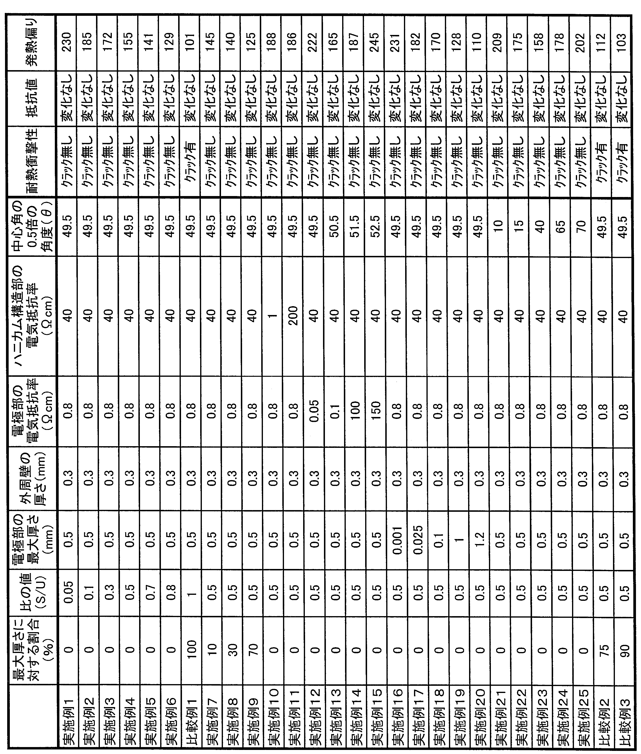
(実施例2~25及び比較例1~3)
ハニカム構造体の電極部及びハニカム構造部を、表1に示す値を満たすように変更したこと以外は、実施例1と同様にしてハニカム構造体を作製した。
ハニカム構造体の電極部及びハニカム構造部を、表1に示す値を満たすように変更したこと以外は、実施例1と同様にしてハニカム構造体を作製した。
得られたハニカム構造体について、上記の方法で、「耐熱衝撃性」、「耐熱衝撃性試験前後の抵抗値」、及び「発熱偏り」の評価を行った。結果を表1に示す。
表1から明らかなように、実施例1~25のハニカム構造体は、触媒担体であると共に電圧を印加することによりヒーターとしても機能し、比較例1~3のハニカム構造体に比べて、耐熱衝撃性に優れることが確認できた。
実施例2~6は、比の値(S/U)が0.1~0.8の範囲内であるため、実施例1に比べて、発熱偏りの評価が良好であることが確認できた。即ち、ハニカム構造体における温度分布の偏りが抑制されていることが確認できた。
実施例14、15は、電極部の電気抵抗率が0.1~100Ωcm範囲内であるため、実施例13、16に比べて、発熱偏りの評価が良好であることが確認できた。即ち、ハニカム構造体における温度分布の偏りが抑制されていることが確認できた。
実施例17~20は、電極部の最大厚さが0.025~3mmの範囲内であるため、実施例16に比べて、発熱偏りの評価が良好であることが確認できた。即ち、ハニカム構造体における温度分布の偏りが抑制されていることが確認できた。
実施例22~24は、電極部の中心角αの0.5倍(中心角αの0.5倍の角度θ)が15~65°であるため、実施例21、25に比べて、発熱偏りの評価が良好であることが確認できた。即ち、ハニカム構造体における温度分布の偏りが抑制されていることが確認できた。
本発明のハニカム構造体は、自動車の排ガスを浄化する排ガス浄化装置用の触媒担体として好適に利用することができる。
1:隔壁、2:セル、3:外周壁、4:ハニカム構造部、4a:ハニカム構造部の一方の端部、4b:ハニカム構造部の他方の端部、5:側面、11:一方の端面、12:他方の端面、13:側端縁、15:外周縁、21:電極部、21a:電極部の一方の端部、21b:電極部の他方の端部、21X:中央部、21Y:拡張部、22:電極端子突起部、22a:基板、22b:突起部、23:導電体、25:肉薄部、26:空洞、27:窪み、100,200,300,400,500,501,502a,502b,503,600,700,800,900:ハニカム構造体、A,B,C:電極部における領域、O:中心、I:セルの延びる方向、M:中央に位置する領域、X:周方向α:中心角、θ:中心角の0.5倍の角度。
Claims (6)
- 流体の流路となる一方の端面から他方の端面まで延びる複数のセルを区画形成する多孔質の隔壁と最外周に位置する外周壁とを有する筒状のハニカム構造部と、前記ハニカム構造部の側面に配設された一対の電極部とを備え、
前記ハニカム構造部の電気抵抗率が、10~200Ωcmであり、
前記一対の電極部のそれぞれが、前記ハニカム構造部のセルの延びる方向に延びる帯状に形成され、
前記セルの延びる方向に直交する断面において、前記一対の電極部における一方の前記電極部が、前記一対の電極部における他方の前記電極部に対して、前記ハニカム構造部の中心を挟んで反対側に配設され、
前記電極部が、前記電極部の最大厚さの0~70%の厚さである部分を有するものであるハニカム構造体。 - 前記電極部には、貫通孔が形成されている請求項1に記載のハニカム構造体。
- 前記電極部の最大厚さは、0.025~3mmである請求項1または2に記載のハニカム構造体。
- 前記一対の電極部のそれぞれが、前記ハニカム構造部の両端部間に亘って形成された請求項1~3のいずれか一項に記載のハニカム構造体。
- 前記電極部の電気抵抗率が、0.01~100Ωcmである請求項1~4のいずれか一項に記載のハニカム構造体。
- 前記電極部の電気抵抗率よりも低い電気抵抗率をもつ導電体が、前記電極部の表面に設置された請求項1~5のいずれか一項に記載のハニカム構造体。
Priority Applications (4)
| Application Number | Priority Date | Filing Date | Title |
|---|---|---|---|
| EP11851723.4A EP2656902B1 (en) | 2010-12-24 | 2011-12-22 | Honeycomb structure |
| JP2012549897A JP5919199B2 (ja) | 2010-12-24 | 2011-12-22 | ハニカム構造体 |
| CN201180062346.9A CN103269771B (zh) | 2010-12-24 | 2011-12-22 | 蜂窝状结构体 |
| US13/922,809 US9516702B2 (en) | 2010-12-24 | 2013-06-20 | Honeycomb structure |
Applications Claiming Priority (2)
| Application Number | Priority Date | Filing Date | Title |
|---|---|---|---|
| JP2010288678 | 2010-12-24 | ||
| JP2010-288678 | 2010-12-24 |
Related Child Applications (1)
| Application Number | Title | Priority Date | Filing Date |
|---|---|---|---|
| US13/922,809 Continuation US9516702B2 (en) | 2010-12-24 | 2013-06-20 | Honeycomb structure |
Publications (1)
| Publication Number | Publication Date |
|---|---|
| WO2012086815A1 true WO2012086815A1 (ja) | 2012-06-28 |
Family
ID=46314080
Family Applications (1)
| Application Number | Title | Priority Date | Filing Date |
|---|---|---|---|
| PCT/JP2011/079937 Ceased WO2012086815A1 (ja) | 2010-12-24 | 2011-12-22 | ハニカム構造体 |
Country Status (5)
| Country | Link |
|---|---|
| US (1) | US9516702B2 (ja) |
| EP (1) | EP2656902B1 (ja) |
| JP (1) | JP5919199B2 (ja) |
| CN (1) | CN103269771B (ja) |
| WO (1) | WO2012086815A1 (ja) |
Cited By (10)
| Publication number | Priority date | Publication date | Assignee | Title |
|---|---|---|---|---|
| WO2013008664A1 (ja) * | 2011-07-11 | 2013-01-17 | 日本碍子株式会社 | ハニカム構造体 |
| JP2013083162A (ja) * | 2011-10-06 | 2013-05-09 | Toyota Motor Corp | 通電加熱式触媒装置 |
| JP2013136966A (ja) * | 2011-12-28 | 2013-07-11 | Toyota Motor Corp | 通電加熱式触媒装置及びその製造方法 |
| JP2014198296A (ja) * | 2013-03-29 | 2014-10-23 | 日本碍子株式会社 | ハニカム構造体 |
| JP2019171345A (ja) * | 2018-03-29 | 2019-10-10 | 日本碍子株式会社 | 電気加熱型触媒用担体 |
| JP2022119537A (ja) * | 2021-02-04 | 2022-08-17 | イビデン株式会社 | 熱交換器及び改質器 |
| JP2022119536A (ja) * | 2021-02-04 | 2022-08-17 | イビデン株式会社 | 熱交換器及び改質器 |
| JP2022119539A (ja) * | 2021-02-04 | 2022-08-17 | イビデン株式会社 | 熱交換器及び改質器 |
| JP2023151176A (ja) * | 2022-03-31 | 2023-10-16 | 日本碍子株式会社 | ハニカム構造体、電気加熱型担体及び排気ガス浄化装置 |
| JP7909394B2 (ja) | 2022-03-31 | 2026-08-21 | Ngk株式会社 | ハニカム構造体、電気加熱型担体及び排気ガス浄化装置 |
Families Citing this family (12)
| Publication number | Priority date | Publication date | Assignee | Title |
|---|---|---|---|---|
| WO2011125815A1 (ja) * | 2010-03-31 | 2011-10-13 | 日本碍子株式会社 | ハニカム構造体 |
| US9422852B2 (en) | 2011-02-08 | 2016-08-23 | Toyota Jidosha Kabushiki Kaisha | Electric heating catalyst |
| JP6131980B2 (ja) * | 2015-03-27 | 2017-05-24 | トヨタ自動車株式会社 | 電気加熱式触媒コンバーター |
| KR101714363B1 (ko) * | 2015-04-16 | 2017-03-23 | 주식회사 엔바이온 | 균열 저항성을 갖는 하니컴 구조체 |
| US10774802B2 (en) * | 2017-05-15 | 2020-09-15 | Phillips & Temro Industries Inc. | Intake air heating system for a vehicle |
| JP7105149B2 (ja) * | 2018-09-11 | 2022-07-22 | 日本碍子株式会社 | 電気加熱型触媒用担体及び排ガス浄化装置 |
| US11215096B2 (en) | 2019-08-21 | 2022-01-04 | Corning Incorporated | Systems and methods for uniformly heating a honeycomb body |
| JP7279609B2 (ja) * | 2019-10-09 | 2023-05-23 | トヨタ自動車株式会社 | 電気加熱式触媒装置 |
| EP4052536A1 (en) * | 2019-10-29 | 2022-09-07 | Corning Incorporated | Systems and methods for heating a honeycomb body |
| WO2021170232A1 (de) * | 2020-02-26 | 2021-09-02 | E.G.O. Elektro-Gerätebau GmbH | Heizeinrichtung |
| JP7523399B2 (ja) * | 2021-03-31 | 2024-07-26 | 日本碍子株式会社 | ハニカム構造体の発熱分布の推定方法、ハニカム構造体の製造方法及び電気加熱式担体の製造方法 |
| JP7682829B2 (ja) * | 2022-03-31 | 2025-05-26 | 日本碍子株式会社 | 柱状ハニカム構造体 |
Citations (12)
| Publication number | Priority date | Publication date | Assignee | Title |
|---|---|---|---|---|
| JPH0467588A (ja) * | 1990-07-06 | 1992-03-03 | Ngk Insulators Ltd | 電極一体型ハニカムヒーター及びその製造方法 |
| JPH04280086A (ja) * | 1991-03-06 | 1992-10-06 | Ngk Insulators Ltd | ハニカムモノリスヒータ |
| JPH08141408A (ja) | 1994-11-24 | 1996-06-04 | Nippon Soken Inc | 排ガス浄化用抵抗調整型ヒータ付触媒担体およびその製造方法 |
| JP2931362B2 (ja) | 1990-04-12 | 1999-08-09 | 日本碍子株式会社 | 抵抗調節型ヒーター及び触媒コンバーター |
| JP2004068684A (ja) * | 2002-08-05 | 2004-03-04 | Ngk Insulators Ltd | 排気ガス処理装置 |
| JP4136319B2 (ja) | 2000-04-14 | 2008-08-20 | 日本碍子株式会社 | ハニカム構造体及びその製造方法 |
| JP2010229978A (ja) * | 2009-03-30 | 2010-10-14 | Ngk Insulators Ltd | 通電加熱型ハニカム体の制御システム |
| JP2010229977A (ja) * | 2009-03-30 | 2010-10-14 | Ngk Insulators Ltd | 排ガス浄化処理装置 |
| WO2011125815A1 (ja) * | 2010-03-31 | 2011-10-13 | 日本碍子株式会社 | ハニカム構造体 |
| WO2011125816A1 (ja) * | 2010-03-31 | 2011-10-13 | 日本碍子株式会社 | ハニカム構造体 |
| WO2011125817A1 (ja) * | 2010-03-31 | 2011-10-13 | 日本碍子株式会社 | ハニカム構造体 |
| JP2011207116A (ja) * | 2010-03-30 | 2011-10-20 | Ngk Insulators Ltd | セラミックス構造体の製造方法 |
Family Cites Families (9)
| Publication number | Priority date | Publication date | Assignee | Title |
|---|---|---|---|---|
| US5266278A (en) | 1990-07-06 | 1993-11-30 | Ngk Insulators, Ltd. | Honeycomb heater having integrally formed electrodes and/or integrally sintered electrodes and method of manufacturing such honeycomb heater |
| US5288975A (en) | 1991-01-30 | 1994-02-22 | Ngk Insulators, Ltd. | Resistance adjusting type heater |
| CA2147112A1 (en) * | 1994-05-26 | 1995-11-27 | Kishor Purushottam Gadkaree | Electrically heatable activated carbon bodies for adsorption and desorption applications |
| JP2003260322A (ja) | 2002-03-08 | 2003-09-16 | Ngk Insulators Ltd | ハニカム構造体、その製造方法及び排ガス浄化システム |
| DE102004016434B4 (de) * | 2004-03-31 | 2006-01-05 | Hermsdorfer Institut Für Technische Keramik E.V. | Elektrischer Fluidheizer |
| WO2007023653A1 (ja) | 2005-08-26 | 2007-03-01 | Ibiden Co., Ltd. | ハニカム構造体及びその製造方法 |
| WO2011125229A1 (ja) * | 2010-04-09 | 2011-10-13 | イビデン株式会社 | ハニカム構造体 |
| WO2011125228A1 (ja) * | 2010-04-09 | 2011-10-13 | イビデン株式会社 | ハニカム構造体 |
| JP5691848B2 (ja) * | 2010-09-27 | 2015-04-01 | 株式会社デンソー | ハニカム構造体及び電気加熱式触媒装置 |
-
2011
- 2011-12-22 EP EP11851723.4A patent/EP2656902B1/en active Active
- 2011-12-22 WO PCT/JP2011/079937 patent/WO2012086815A1/ja not_active Ceased
- 2011-12-22 JP JP2012549897A patent/JP5919199B2/ja active Active
- 2011-12-22 CN CN201180062346.9A patent/CN103269771B/zh active Active
-
2013
- 2013-06-20 US US13/922,809 patent/US9516702B2/en active Active
Patent Citations (12)
| Publication number | Priority date | Publication date | Assignee | Title |
|---|---|---|---|---|
| JP2931362B2 (ja) | 1990-04-12 | 1999-08-09 | 日本碍子株式会社 | 抵抗調節型ヒーター及び触媒コンバーター |
| JPH0467588A (ja) * | 1990-07-06 | 1992-03-03 | Ngk Insulators Ltd | 電極一体型ハニカムヒーター及びその製造方法 |
| JPH04280086A (ja) * | 1991-03-06 | 1992-10-06 | Ngk Insulators Ltd | ハニカムモノリスヒータ |
| JPH08141408A (ja) | 1994-11-24 | 1996-06-04 | Nippon Soken Inc | 排ガス浄化用抵抗調整型ヒータ付触媒担体およびその製造方法 |
| JP4136319B2 (ja) | 2000-04-14 | 2008-08-20 | 日本碍子株式会社 | ハニカム構造体及びその製造方法 |
| JP2004068684A (ja) * | 2002-08-05 | 2004-03-04 | Ngk Insulators Ltd | 排気ガス処理装置 |
| JP2010229978A (ja) * | 2009-03-30 | 2010-10-14 | Ngk Insulators Ltd | 通電加熱型ハニカム体の制御システム |
| JP2010229977A (ja) * | 2009-03-30 | 2010-10-14 | Ngk Insulators Ltd | 排ガス浄化処理装置 |
| JP2011207116A (ja) * | 2010-03-30 | 2011-10-20 | Ngk Insulators Ltd | セラミックス構造体の製造方法 |
| WO2011125815A1 (ja) * | 2010-03-31 | 2011-10-13 | 日本碍子株式会社 | ハニカム構造体 |
| WO2011125816A1 (ja) * | 2010-03-31 | 2011-10-13 | 日本碍子株式会社 | ハニカム構造体 |
| WO2011125817A1 (ja) * | 2010-03-31 | 2011-10-13 | 日本碍子株式会社 | ハニカム構造体 |
Non-Patent Citations (1)
| Title |
|---|
| See also references of EP2656902A4 |
Cited By (15)
| Publication number | Priority date | Publication date | Assignee | Title |
|---|---|---|---|---|
| WO2013008664A1 (ja) * | 2011-07-11 | 2013-01-17 | 日本碍子株式会社 | ハニカム構造体 |
| US9382831B2 (en) | 2011-07-11 | 2016-07-05 | Ngk Insulators, Ltd. | Honeycomb structure |
| JP2013083162A (ja) * | 2011-10-06 | 2013-05-09 | Toyota Motor Corp | 通電加熱式触媒装置 |
| JP2013136966A (ja) * | 2011-12-28 | 2013-07-11 | Toyota Motor Corp | 通電加熱式触媒装置及びその製造方法 |
| JP2014198296A (ja) * | 2013-03-29 | 2014-10-23 | 日本碍子株式会社 | ハニカム構造体 |
| US9506391B2 (en) | 2013-03-29 | 2016-11-29 | Ngk Insulators, Ltd. | Honeycomb structure |
| JP2019171345A (ja) * | 2018-03-29 | 2019-10-10 | 日本碍子株式会社 | 電気加熱型触媒用担体 |
| JP2022119537A (ja) * | 2021-02-04 | 2022-08-17 | イビデン株式会社 | 熱交換器及び改質器 |
| JP2022119536A (ja) * | 2021-02-04 | 2022-08-17 | イビデン株式会社 | 熱交換器及び改質器 |
| JP2022119539A (ja) * | 2021-02-04 | 2022-08-17 | イビデン株式会社 | 熱交換器及び改質器 |
| JP7633820B2 (ja) | 2021-02-04 | 2025-02-20 | イビデン株式会社 | 熱交換器及び改質器 |
| JP7633819B2 (ja) | 2021-02-04 | 2025-02-20 | イビデン株式会社 | 熱交換器及び改質器 |
| JP7633818B2 (ja) | 2021-02-04 | 2025-02-20 | イビデン株式会社 | 熱交換器及び改質器 |
| JP2023151176A (ja) * | 2022-03-31 | 2023-10-16 | 日本碍子株式会社 | ハニカム構造体、電気加熱型担体及び排気ガス浄化装置 |
| JP7909394B2 (ja) | 2022-03-31 | 2026-08-21 | Ngk株式会社 | ハニカム構造体、電気加熱型担体及び排気ガス浄化装置 |
Also Published As
| Publication number | Publication date |
|---|---|
| EP2656902A4 (en) | 2016-10-12 |
| CN103269771B (zh) | 2015-09-30 |
| US20130277360A1 (en) | 2013-10-24 |
| JPWO2012086815A1 (ja) | 2014-06-05 |
| JP5919199B2 (ja) | 2016-05-18 |
| US9516702B2 (en) | 2016-12-06 |
| EP2656902A1 (en) | 2013-10-30 |
| CN103269771A (zh) | 2013-08-28 |
| EP2656902B1 (en) | 2018-03-21 |
Similar Documents
| Publication | Publication Date | Title |
|---|---|---|
| JP5919199B2 (ja) | ハニカム構造体 | |
| JP5663003B2 (ja) | ハニカム構造体 | |
| JP5658233B2 (ja) | ハニカム構造体 | |
| JP5850858B2 (ja) | ハニカム構造体 | |
| JP5654999B2 (ja) | ハニカム構造体 | |
| JP5658234B2 (ja) | ハニカム構造体 | |
| JP5792743B2 (ja) | ハニカム構造体 | |
| JP5860465B2 (ja) | ハニカム構造体 | |
| JP5735481B2 (ja) | ハニカム構造体 | |
| JP6126434B2 (ja) | ハニカム構造体 | |
| JP5902670B2 (ja) | ハニカム構造体 | |
| JP5916628B2 (ja) | ハニカム構造体 | |
| JP5749894B2 (ja) | ハニカム構造体 | |
| CN110314705B (zh) | 蜂窝结构体 | |
| WO2013146955A1 (ja) | ハニカム構造体 | |
| JP2019171345A (ja) | 電気加熱型触媒用担体 | |
| JP6038711B2 (ja) | ハニカム構造体及びその製造方法 |
Legal Events
| Date | Code | Title | Description |
|---|---|---|---|
| 121 | Ep: the epo has been informed by wipo that ep was designated in this application |
Ref document number: 11851723 Country of ref document: EP Kind code of ref document: A1 |
|
| ENP | Entry into the national phase |
Ref document number: 2012549897 Country of ref document: JP Kind code of ref document: A |
|
| NENP | Non-entry into the national phase |
Ref country code: DE |
|
| WWE | Wipo information: entry into national phase |
Ref document number: 2011851723 Country of ref document: EP |