WO2012090242A1 - 電力変換器及び太陽光発電システム - Google Patents
電力変換器及び太陽光発電システム Download PDFInfo
- Publication number
- WO2012090242A1 WO2012090242A1 PCT/JP2010/007560 JP2010007560W WO2012090242A1 WO 2012090242 A1 WO2012090242 A1 WO 2012090242A1 JP 2010007560 W JP2010007560 W JP 2010007560W WO 2012090242 A1 WO2012090242 A1 WO 2012090242A1
- Authority
- WO
- WIPO (PCT)
- Prior art keywords
- current
- power
- mode
- target value
- solar cell
- Prior art date
- Legal status (The legal status is an assumption and is not a legal conclusion. Google has not performed a legal analysis and makes no representation as to the accuracy of the status listed.)
- Ceased
Links
Images





Classifications
-
- G—PHYSICS
- G05—CONTROLLING; REGULATING
- G05F—SYSTEMS FOR REGULATING ELECTRIC OR MAGNETIC VARIABLES
- G05F1/00—Automatic systems in which deviations of an electric quantity from one or more predetermined values are detected at the output of the system and fed back to a device within the system to restore the detected quantity to its predetermined value or values, i.e. retroactive systems
- G05F1/66—Regulating electric power
- G05F1/67—Regulating electric power to the maximum power available from a generator, e.g. from solar cell
Definitions
- the present invention relates to a system that obtains desired power by converting power generated by a solar cell using a power converter, and in particular, by controlling a converter connected to the solar cell, the maximum point of power of the solar cell is determined.
- the present invention relates to a maximum power tracking control method for detecting and operating a converter at a detected maximum power point.
- FIG. 4 is a graph showing current-voltage characteristics and current-power characteristics of the solar cell.
- This hill-climbing method minutely changes the input voltage command value of the power converter, and determines whether the generated power of the solar cell increases or decreases according to this. Then, based on this determination result, a change direction for changing the next voltage command value to slightly increase or decrease is determined, and the command value is minutely changed repeatedly.
- Japanese Patent No. 4294346 there is a method disclosed in Japanese Patent No. 4294346.
- This method has a power conversion circuit having a configuration in which an inductor and a switching element are connected in series to two terminals of a solar cell. When a maximum power point is detected, the switching element is held in an on state to flow through the inductor. By changing the current from zero to short-circuit current, the current-voltage characteristics at this time are scanned to detect the current and voltage at the maximum power point, and the operating point of the solar cell is the current at the maximum power point obtained by scanning, The power conversion circuit is operated so as to be a voltage. Since this method can scan the entire current-voltage characteristics of the solar cell at high speed, it is faster in response than the hill-climbing method. Is possible.
- the above hill-climbing method has a risk of slow response. In addition, there is a fear that it is not possible to cope with the double peak characteristics that occur when a partial shadow occurs in the solar cell.
- the scanning method disclosed in Patent Document 1 described above flows into the choke coil L of the power conversion circuit by keeping the switching element on when scanning the characteristics of the current Ipv-voltage Vpv of the solar cell.
- L value inductance value
- the choke coil needs to have an inductance value equal to or higher than the lower limit value. In the scan method of Patent Document 1, it may be difficult to improve the trade-off between the reduction in the volume of the choke coil and the detection accuracy.
- the problems to be solved by the present invention include improvement in responsiveness, response to partial shadows, reduction in volume and weight of the choke coil of the power converter in the photovoltaic power generation system, and cost reduction. By ensuring the detection accuracy of the maximum power point, it is to realize a small, light and low cost photovoltaic power generation system which always has a high MPPT efficiency.
- the present invention provides a solar power generation system having a solar cell and a power converter connected to the solar cell, wherein the power converter flows into the power converter from at least one switching element and a solar cell.
- the power converter flows into the power converter from at least one switching element and a solar cell.
- the current control means is operated while increasing sequentially from the above, and each time the power at that time is calculated from the input current and the input voltage, and the power There characterized in that it has a steady-state mode for operating said current control means with a detection mode for obtaining the current target value of the point having the maximum the current target value determined by the detection mode.
- the mode may transition to the steady mode after a predetermined time has elapsed, or may transition to the steady mode when the input voltage drops below a predetermined value.
- the transition from the steady mode to the detection mode is performed at regular intervals, and at that time, the power of the steady mode fluctuates by a predetermined ratio or more with respect to the maximum power detected in the detection mode. In some cases, it is also effective to transition to the detection mode without waiting for the elapse of the predetermined time.
- the target value variable means can change the current target value by increasing the current target value by increasing the current target value after exceeding a current value smaller than the current target value used in the previous steady mode.
- the rate of increase of the target value variable means is moderate compared to the outside of the predetermined width when it is within a predetermined width based on the current target value in the previous steady mode. May be.
- the other power converter when there are a plurality of the power converters and one of the power converters is in the detection mode, the other power converter is set to the steady mode, or the operation of the steady mode is performed once. Assuming that time is T and n is the number of power converters in parallel, it is also effective means that each power converter transitions from the steady mode to the detection mode with a delay of T / n.
- the detection mode and the steady mode are repeated, and the current increase rate of the current target value varying means in the detection mode of the plurality of times is higher than that of the previous time in the detection mode.
- the increase rate may be used as the current increase rate of the current target value varying means in the subsequent detection mode.
- the power converter has a function of a step-up / down converter, and in the detection mode, the current target value may be increased to make a transition from the step-down operation to the step-up operation.
- the current obtained in the immediately preceding detection mode may be used.
- the target value is slightly increased or decreased, and as a result, the increase or decrease in power is determined from the input voltage and current changed, and the current target value is decreased in the direction in which the power increases. It may be changed.
- a solar power generation system in which a solar cell, a power converter, and a commercial system are connected, wherein the power converter has a detection mode and a steady mode for detecting the maximum power of the solar cell, and the detection mode also includes the detection mode
- the problem of the present invention can also be solved by having a function of outputting the power of the solar cell from the power converter to the commercial system.
- the present invention relates to a current target for controlling the current of the solar cell when detecting the maximum power point of the solar cell in a power converter that performs tracking control so that the solar cell operates at the maximum power point. Once the value is changed to a predetermined current value, the power of the solar cell is sampled and the maximum power point is detected while changing every predetermined current width from the predetermined current value to the short-circuit current.
- the present invention relates to a current target for controlling the current of the solar cell when detecting the maximum power point of the solar cell in a power converter that performs tracking control so that the solar cell operates at the maximum power point.
- a current target for controlling the current of the solar cell when detecting the maximum power point of the solar cell in a power converter that performs tracking control so that the solar cell operates at the maximum power point.
- the detection control mode is a current target.
- a target value setting step for determining a value, a current control step for controlling the output current to a value substantially equal to the current target value, a current / voltage detection step for detecting the output current and the output voltage, and the output current
- a power / current storage step for storing power obtained by multiplication with the output voltage and an output current at that time, wherein the current target value gradually increases in the target value setting step, and the power / current storage
- the power stored in the previous power / current storage step is compared with the current power, and the larger power and the output current at that time are stored.
- the detection control mode transitions to the steady control mode after a lapse of a predetermined time, and in the steady control mode, the output current and output voltage of the solar cell are calculated according to the maximum power point that is the power stored in the power / current storage step. It is characterized by controlling.
- the present invention provides the detection control mode in which the maximum power point of the solar cell is detected from the output current and the output voltage of the solar cell, and the maximum power point tracking control method of the solar cell that includes the steady control mode.
- the mode is a target value setting step for determining a current target value, a current control step for controlling the output current to a value substantially equal to the current target value, a current / voltage detection step for detecting the output current and the output voltage, A power / current storage step for storing the power obtained by multiplying the output current and the output voltage and the output current at that time, and in the target value setting step, the current target value gradually increases,
- the power stored in the previous power / current storage step is compared with the current power, and the larger power and the output power at that time are compared.
- the detection control mode ends when the voltage detected in the current / voltage detection step reaches a predetermined value and transitions to the steady control mode.
- the power / current is The output current and output voltage of the solar cell are controlled according to the maximum power point that is the power stored in the storing step.
- the present invention provides the detection control mode in which the maximum power point of the solar cell is detected from the output current and the output voltage of the solar cell, and the maximum power point tracking control method of the solar cell that includes the steady control mode.
- the mode is a target value setting step for determining a current target value, a current control step for controlling the output current to a value substantially equal to the current target value, a current / voltage detection step for detecting the output current and the output voltage, A power / current storage step for storing the power obtained by multiplying the output current and the output voltage and the output current at that time, and in the target value setting step, the current target value gradually increases,
- the detection control mode ends when the voltage detected in the current / voltage detection step reaches a predetermined value, and transitions to the steady control mode. In the control mode of the power stored in said power-current storage step, and controlling the output current and the output voltage of the solar cell in accordance with the maximum power point of maximum power.
- the present invention includes a step of detecting an output voltage and an output current of a solar cell, a step of determining a target value of the output current, a step of controlling the output current to a value substantially equal to the target value, and the output A step of storing the power obtained by multiplying the current by the output voltage and the output current at that time, the target value gradually increasing in the step of determining the target value, and the previous power / current storage in the step of storing The power stored in the step is compared with the current power, and the larger power and the output current at that time are stored.
- the time change rate of the current does not depend on the inductance value of the choke coil but depends on the increasing rate of the set current target value. For this reason, the inductance value of the choke coil can be freely set while ensuring excellent response to the detection accuracy of the maximum power point and the temperature change, aging, and partial shadow occurrence of the solar cell characteristics of the conventional scanning method. It becomes possible to select.
- the inductance value of the choke coil of the power converter in the photovoltaic power generation system takes into consideration the optimum switching frequency determined from the speed of the switching element and diode, switching loss, ripple current on the output side, and the like. Can be selected. For this reason, the inductance value of a choke coil can be reduced more than before by using a high-speed switching element. As a result, the volume of the choke coil can be reduced and the weight of the choke coil can be reduced. When the inductance of the choke coil is reduced, the length of the copper wire that is the material of the choke coil can be shortened, and the core volume made of the ferrite material can be reduced. As a result, the choke coil is small and light, and the cost can be reduced.
- a low-inductance choke coil can be mounted on a substrate, contributing to a reduction in the number of man-hours when manufacturing power conditioners.
- An example of the circuit structure of the input filter of FIG. The graph which shows the current-voltage characteristic and current-power characteristic of a solar cell.
- the PAD figure which shows a stationary mode among the control algorithms of Example 2 of this invention.
- FIG. 9 is a block diagram showing a circuit configuration of a fifth embodiment of the present invention.
- the following configuration is proposed in order to contribute to the realization of a small, lightweight and low-cost solar power generation system.
- FIG. 1 A first embodiment of the present invention will be described with reference to FIG. 1, FIG. 2, FIG. 3, and FIG.
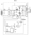
- FIG. 1 is a diagram showing a circuit configuration of Embodiment 1 of the present invention.
- 1 is a solar panel
- 2 is a power conditioner
- 3 is a commercial system
- 4 is an input filter
- 7 is a DC-DC converter
- 8 is a choke coil
- 9 is a power MOSFET
- 10 is a boost diode
- 11 is a capacitor
- 12 is a grid interconnection inverter
- 13 is a current sensor
- 14 is a control circuit
- 15a and 15b are voltage dividing resistors
- 16 is a target value variable means
- 17 is a mode switch
- 18 is a subtractor
- 19 is PI.
- a control block, 20 is a multiplier
- 21a and 21b are AD converters
- 22a is a PWM circuit
- 23 is a maximum value determination circuit.
- the power conditioner 2 includes an input filter 4, a DC-DC converter 7, a grid interconnection inverter 12, and a control circuit 14. Both ends of the solar cell panel 1 are connected to the input side terminals of the input filter 4 inside the power conditioner 2, and the converter side terminal of the input filter 4 is connected to the DC-DC converter 7. Is connected to the grid interconnection inverter 12.
- the grid interconnection inverter 12 is connected to the commercial system 3 outside the power conditioner 2.
- the DC-DC converter 7 includes a choke coil 8, voltage dividing resistors 15a and 15b, a power MOSFET 9, a boost diode 10, a capacitor 11, and a current sensor 13, and the choke coil 8 and the drain of the power MOSFET 9 are connected. Yes.
- the input side of the choke coil 8 is connected to the converter side terminal of the input filter 4.
- the source of the power MOSFET 9 is connected to the converter side terminal of the input filter 4.
- Voltage dividing resistors 15 a and 15 b are connected in series at both ends of the converter side terminal of the input filter 4 and inside the DC-DC converter 7.
- the anode of the boost diode 10 is connected to the drain of the power MOSFET 9.
- a capacitor 11 is connected between the cathode of the boost diode 10 and the source of the power MOSFET 9. Both ends of the capacitor 11 are connected to the grid interconnection inverter 12 outside the DC-DC converter 7.
- AD converters 21a and 21b, target value variable means 16, mode switcher 17, subtractor 18, PI control block 19, multiplier 20, PWM circuit 22a, and maximum value determination circuit 23 are provided. is there.
- the current sensor 13 is connected to the AD converter 21b. If the current flowing through the choke coil 8 is IL, the output of the AD converter 21b is ILave, which is the average value of IL, and the output of the AD converter 21a is Vin. ILave and Vin are input to the multiplier 20, and the output is input to the maximum value determination circuit 23 as Ppv. ILave is input to the minus terminal of the subtractor 18. The Iref that is the output of the mode switch 17 is connected to the plus side input terminal of the subtractor 18. The output of the subtracter 18 is input to the PI control block 19. Iref is input to the maximum value determination circuit 23.
- the output of the PI control block 19 is input to the PWM circuit 22a.
- the output of the PWM circuit 22a is output to the outside of the control circuit 14 as the S1 control signal and is connected to the gate of the power MOSFET 9 inside the DC-DC converter 7.
- the output of the maximum value determination circuit 23 is connected to the stationary side of the mode switch 17 as IrefM.
- a target value variable means 16 is connected to the detection side of the mode switch 17.
- the current target value Iref is output from the mode switch 17 and is a target value of the current IL flowing through the choke coil 8.
- FIG. 2 shows the circuit operation of the first embodiment, and shows the operation waveform of each part of the circuit of FIG. 1 with the horizontal axis as time.
- the operation state of the DC-DC converter 7 is distinguished between the steady mode and the detection mode, and as Vpv, the voltage waveforms in the steady mode and the detection mode at both ends of the solar cell panel 1 in FIG. 1, the current target values Iref and S1 control.
- the detection mode is a mode for detecting the maximum power point of the solar cell
- the steady mode is a power converter (power conditioner 2) so that the current at the maximum power point obtained in the detection mode is obtained. ).
- FIG. 3 is a diagram showing an example of the inside of the input filter 4 in FIG.
- 5a and 5b are common mode chokes
- 6a, 6b, 6c, 6d and 6e are filter capacitors
- 27 is a normal mode choke.
- a filter capacitor 6a is connected to both ends of the input side terminal of the input filter 4
- an input side terminal of the common mode choke 5a is connected to both ends of the filter capacitor 6a.
- the output side terminal of the common mode choke 5a is connected to a series body of filter capacitors 6b and 6c.
- the midpoint of the filter capacitors 6b and 6c is connected to the frame ground.
- Both ends of the filter capacitor 6d are connected to both ends of the series body of the filter capacitors 6b and 6c.
- Both ends of the filter capacitor 6d are connected to the input side terminals of the common mode choke 5b.
- a normal mode choke 27 is connected to one of output terminals of the common mode choke 5b, and a filter capacitor 6e is connected between the normal mode choke 27 and the other terminal of the common mode choke 5b. Then, both terminals of the filter capacitor 6 e become the converter side terminals and are drawn out of the input filter 4.
- FIG. 4 is a graph showing the current-voltage characteristics and current-power characteristics of the solar cell, with the horizontal axis representing the current Ipv of the solar cell panel 1, the vertical axis representing the voltage Vpv (left side), and the power Ppv (right side). As a solid line, the characteristics of the output current Ipv and the voltage Vpv of the solar cell panel 1 are shown. On the other hand, the dotted line indicates the characteristics of the output current Ipv and the power Ppv of the solar cell panel 1.
- the mode switch 17 in FIG. 1 is connected to the steady mode side. Therefore, the current target value Iref is IrefM that is the output of the maximum value determination circuit 23.
- IrefM in the stationary mode period before the detection mode in FIG. 2 is defined as IrefM (n ⁇ 1)
- IrefM in the stationary mode period after the detection mode in FIG. 2 is defined as IrefM (n). Therefore, if the current time is the steady mode before the detection mode in FIG. 2, the current target value is IrefM (n ⁇ 1).
- the DC-DC converter 7 performs a current control operation so that the average value ILave of the current flowing through the choke coil 8 (L) matches IrefM (n ⁇ 1).
- the current flowing through the choke coil 8 (L) is detected by the current sensor 13. Since the current IL flowing through the choke coil 8 (L) pulsates by switching of the power MOSFET 9 described later, the current IL detected by the current sensor 13 is taken into the control circuit 14 via the AD converter 21b and recognized as the average value ILave.
- the As a method for extracting the average value ILave from the pulsating current IL there is a method of providing a first-order lag filter for attenuating the switching frequency component of the power MOSFET 9 (S1) in the current sensor 13, or a timing at which the AD converter 21a is taken in by a PWM cycle. There is a method of always sampling the central value of the pulsation in synchronization with the pulsation, and any method may be used as long as the average value ILave can be extracted from the pulsating current IL. This ILave is subtracted from the current target value Iref in the subtractor 18.
- Iref IrefM (n ⁇ 1)
- IrefM the current error which is the output of the subtractor 18
- IrefM the current error which is the output of the subtractor 18
- ILave This current error is input to the PI control block 19 and is subjected to proportional integration calculation.
- the output of the PI control block 19 is a duty ratio, and this duty ratio is input to the PWM circuit 22a to generate a PWM pulse.
- This PWM pulse is an S1 control signal and has a pulse waveform as shown in FIG.
- the S1 control signal is input to the gate of the power MOSFET 9 (S1) and drives the power MOSFET 9 (S1).
- the power MOSFET 9 (S1) is repeatedly turned on and off by switching.
- ILave becomes a constant value equal to IrefM (n ⁇ 1) as shown by a dotted line, and the waveform of IL increases during the period when the power MOSFET 9 (S1) is ON as shown by a solid line. However, the power MOSFET 9 (S1) decreases during the OFF period.
- the ILave waveform passes through the center of the IL waveform.
- the current error IrefM (n ⁇ 1) ⁇ ILave is not limited to zero control, but may be controlled to be a value close to zero.
- the pulsation component of IL due to the switching of the power MOSFET 9 (S1) is cut mainly by the normal mode choke 27 and the filter capacitor 5e, and flows into the DC-DC converter 7 from the solar cell panel 1.
- the current Ipv to be performed has substantially the same DC value as ILave.
- the voltage Vpv of the solar cell panel 1 input to the input filter 4 and the output voltage Vin of the input filter 4 have substantially the same DC component, and Vin includes a high-frequency component accompanying switching.
- the grid interconnection inverter 12 converts the DC power input from the DC-DC converter 7 into a sine wave current synchronized with the voltage phase of the commercial system 3 and outputs the sine wave current to the commercial system 3.
- the transition to the detection mode is made after a certain time has elapsed in the steady mode.
- the detection mode is started by switching the mode switch 17 in FIG. 1 to the detection mode side.
- the initial value of the target value varying means 16 is set to zero.
- Iref becomes zero from IrefM (n ⁇ 1) in the steady mode so far.
- the average value ILave of the current flowing through the choke coil 8 (L) is not changed from the normal mode until then, and is subtracted from the current target value Iref in the subtractor 18.
- the current error that is the output of the subtractor 18 is ⁇ ILave.
- This current error is input to the PI control block 19 and is subjected to proportional integration calculation.
- the output of the PI control block 19 is a duty ratio, and this duty ratio is input to the PWM circuit 22a to generate a PWM pulse.
- This PWM pulse is an S1 control signal and has a pulse waveform as shown in FIG.
- the S1 control signal is input to the gate of the power MOSFET 9 (S1) and drives the power MOSFET 9 (S1). When the power MOSFET 9 (S1) is turned on, excitation energy is stored in the choke coil 8 (L) and IL increases.
- ILave that is, the average value of IL (dotted line) decreases to zero
- Vpv increases to Voc.
- a method of stopping the switching of the power MOSFET 9 for a certain time at the beginning of the detection mode may be used.
- ILave is kept substantially equal to Iref, and therefore IL increases following the increase in Iref.
- Ipv is substantially equal to ILave due to the action of the input filter 4, so that Ipv gradually increases from zero in the detection mode.
- Vpv changes according to the characteristic of the solid line shown in FIG.
- ILave and Vin are sampled by the AD converters 21a and 21b each time.
- the sampling period ts is shorter than the time tx when Iref changes.
- the maximum value determination circuit 23 calculates Ppv and Iref at that time as (Ppv, Iref ).
- the detection mode is executed for a period of Ts as shown in FIG. tx * Isc / ⁇ Iref ⁇ Ts Therefore, the current target value Iref reaches or exceeds Isc by Ts.
- the power MOSFET 9 operates with the maximum on-time width set in advance by the PWM circuit 22a. To do.
- the maximum value determination circuit 23 stores (Pmax, Ipmax) as (PMax, IrefM).
- the maximum value determination circuit 23 outputs Ipmax as IrefM.
- the time in the steady mode is T, the time is sufficiently longer than the time Ts in the detection mode.
- the detection mode time Ts is on the order of 1 ms to several tens of ms
- the steady mode time T is on the order of 1 s to several minutes.
- the inductance value of the choke coil 8 used at this time is a value approximately between 100 ⁇ H and 1 mH, and can be mounted on a printed circuit board.
- di / dt in the detection mode does not depend on the inductance value of the choke coil 8, but depends on the increasing rate of the current target value to be set. Therefore, the inductance value of the choke coil can be freely set. This makes it possible to select a solar power generation system that is small, light, and low in cost.
- the maximum power point of the solar cell panel is detected every predetermined time, and the power conditioner can be operated at the detected maximum power point.
- the electric power of the solar cell panel 1 is output from the DC-DC converter 7 and output to the commercial system 3 side via the system interconnection inverter 12. For this reason, even if di / dt is made small in order to improve the detection accuracy, that is, the increase rate of the current change is slowed and the detection mode is extended, the loss of power from the solar cell panel can be minimized. .
- the configuration of the DC-DC converter 7 is preferably the step-up converter shown in FIG. 1, but may be other non-insulated converters or isolated converters.
- the input filter 4 may have other functions as long as it has a similar function, that is, a circuit configuration that prevents the current of the switching component from flowing to the solar cell panel side and reduces common mode noise.
- the control circuit may be constituted by an analog circuit having a similar function.
- the PWM circuit 22a is a circuit that performs pulse width modulation control, it can be replaced by pulse frequency modulation control (PFM), pulse density modulation control (PDM), or the like.
- the PI control block 19 is a block that performs proportional-integral control, but may be configured by an analog circuit such as an operational amplifier as described above, or may be replaced by PID (proportional-integral delay) control or the like.
- the initial value of the target value varying means 16 is set to zero, but this is not restrictive.
- the reason why the initial value of the target value varying means 16 is set to zero is that it also means that there is no leakage in sampling when detecting the maximum power point. Therefore, the initial value of the target value varying means 16 is not limited to zero, and may be a value close to zero.
- the value of the target value variable means 16 may be changed to zero or a value close to zero by gradually reducing the value of the target value variable means 16 when transitioning from the steady mode to the detection mode.
- gradually reducing the value of the target value varying means 16 it is possible to prevent a voltage jump due to the parasitic inductance of the cable between the solar cell panel 1 and the power conditioner 2.
- the timing for gradually increasing the current target value Iref from zero or a value close to zero is when the case where the ILave is zero or a value close to zero is detected, or when a certain time has elapsed. It may be when a certain number of switching times is counted.
- the maximum value determination circuit 23 sets Ppv as the maximum power point PMax when Ppv is larger than the previous set (Ppv, Iref), and Iref at that time is IrefM. However, this is not the case. Since it is only necessary to know the maximum power point PMax, all of the pairs (Ppv, Iref) sequentially input by the maximum value determination circuit 23 are stored, and the largest stored Ppv may be used as the maximum power point PMax. . In this case, Iref at the maximum power point PMax is set to IrefM, and the subsequent steady mode is as described above for outputting Ipmax as IrefM.
- the transition from the steady mode to the detection mode is made after a lapse of a fixed time, but this is not restrictive. It is only necessary to provide a timing for transition from the steady mode to the detection mode, and transition may be performed under a predetermined condition such as the number of times of switching.
- the detection mode is changed to the steady mode after a lapse of a certain time, but this is not restrictive.
- the transition from the detection mode to the steady mode may be performed at the stage where the detection mode is completed or the stage where the maximum power point is detected, and the transition may be performed under a predetermined condition such as the number of times of switching.
- the target current value is determined by the target value varying means 16, but this is not restrictive.
- a voltage value may be used instead of a current value.
- the increase amount ⁇ Iref is set to a minute amount, but this is not restrictive.
- FIG. 5 is a diagram showing a circuit configuration of the present invention, and the same components as those in FIG. 1 are given the same symbols.
- 28 is a control block.
- FIG. 5 is a diagram showing a circuit configuration of the second embodiment of the present invention.
- AD converters 21a and 21b Inside the control circuit 14, there are AD converters 21a and 21b, a subtractor 18, a PI control block 19, a PWM circuit 22a, and a control block 28. And it connects to AD converter 21a from the midpoint of voltage dividing resistance 15a, 15b.
- the current sensor 13 is connected to the AD converter 21b.
- the output of the AD converter 21b is ILave which is an average value of IL, and the output of one AD converter 21a is Vin.
- ILave and Vin are input to the control block 28 for information processing.
- the output of the control block 28 is Iref and is connected to the plus side input terminal of the subtractor 18. ILave is also input to the minus terminal of the subtractor 18.
- the output of the subtracter 18 is input to the PI control block 19.
- the output of the PI control block 19 is input to the PWM circuit 22a.
- the output of the PWM circuit 22a is output to the outside of the control circuit 14 as the S1 control signal and is connected to the gate of the power MOSFET 9 inside the DC-DC converter 7.
- FIG. 6 is a PAD diagram showing the detection mode in the control algorithm of the second embodiment of the present invention
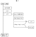
- FIG. 7 is a PAD diagram showing the steady mode in the control algorithm of the second embodiment of the present invention.
- FIG. 6 is a PAD diagram showing the processing contents inside the control block 28 of FIG. 5, and shows the processing contents of the detection mode.
- FIG. 7 is a PAD diagram showing the processing contents of the same control block 28, showing the processing contents of the steady mode.
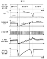
- FIG. 8 is a diagram showing an operation waveform of each part in the present embodiment.
- the L current average value ILave and the input voltage Vin are converted into digital signals by the AD converters 21b and 21a, respectively, and input to the control block 28, regardless of the detection mode or the steady mode. Is output.
- the PWM circuit 22a converts the duty ratio into a pulse width, and performs switching control of the gate of the power MOSFET 9 (S1) as an S1 control signal.
- S1 power MOSFET 9
- Vmin is set in advance.
- Vmin may be a value of 0 V or more.
- Vin> Vmin that is, until the voltage Vpv between terminals of the solar cell is lowered to Vmin.
- the operation is to add the current target value Iref to the current Iref, add ⁇ Iref, read ILave and Vin, calculate the power Ppv by the product of them, and if Ppv is greater than PMax, the maximum power value PMax Is the current Ppv and at the same time IrefM is the current Iref. Repeat the above steps.
- IrefM is output as Iref which is the output of the control block 28.
- the detection mode is completed by the operations so far, and the mode is changed to the steady mode. As shown in the Ppv waveform of FIG. 8, the detection mode end determination is performed at a point ( ⁇ mark) where Vpv is lower than Vmin, and transitions to the steady mode.
- the time obtained by adding ⁇ t to the current t is set to t.
- T which is a predetermined steady mode time.
- > ⁇ P it indicates that the power generation characteristics of the solar cell panel 1 such as sudden change in sunshine and generation of shadows have suddenly changed from the characteristics measured in the previous detection mode.
- high MPPT efficiency can be maintained by redoing the detection mode to obtain a new maximum power value.
- the transition from the steady mode to the detection mode is made after a lapse of a fixed time, but the present invention is not limited to this. It is only necessary to provide a timing for transition from the steady mode to the detection mode, and transition may be performed under a predetermined condition such as the number of times of switching.
- the end of the detection mode described above is the input voltage, that is, the voltage of the solar panel 1 is zero or The point that it judges by decreasing to near zero is mentioned.
- the configuration of the DC-DC converter 7 is preferably the step-up converter shown in FIG. 5, but may be other non-insulated converters or isolated converters.
- the input filter 4 may have a circuit configuration that serves to prevent the current of the switching component from flowing to the solar cell panel side and reduce common mode noise.
- the control circuit 14 may be constituted by an analog circuit having a similar function.
- the control circuit 14 may be a microcomputer or a DSP, and the AD converters 21a and 21b may be installed outside the control circuit 14 to input the digitally converted state quantity to the control circuit 14.
- the PWM circuit 22a is a circuit that performs pulse width modulation control, it can be replaced by pulse frequency modulation control (PFM), pulse density modulation control (PDM), or the like.
- the PI control block 19 is a block that performs proportional-integral control, but may be configured by an analog circuit such as an operational amplifier, or may be replaced by PID (proportional-integral delay) control or the like.
- FIG. 9 is a diagram showing the time change of the current target value in the detection mode of the present invention.
- FIG. 9 shows the mode transition, and the lower part shows the change of the current target value according to the mode transition.
- the horizontal axis is time.
- the current target value Iref in the previous steady mode is IrefM (n ⁇ 1).
- Iref In the detection mode, Iref once becomes zero, and increases with time at an increase rate a of current change as shown in the figure.
- the current change becomes an increase rate b.
- the increase rate b is slower than the previous increase rate a, and the slope (di / dt) of the current target value Iref becomes gentle, so that high detection accuracy can be obtained in the vicinity of IrefM (n ⁇ 1).
- the time of the detection mode can be shortened by setting the time change of the current to the increase rate a. As described above, in this embodiment, it is possible to solve the conflicting problems of the detection mode time reduction and the detection accuracy improvement.
- Iref is once set to zero, but this is not a limitation.
- the initial value of Iref is once set to zero because it also means that there is no leakage in sampling when detecting the maximum power point. Therefore, the initial value of Iref may be a value close to zero instead of zero.
- the timing at which the increase rate a changes to the increase rate b is when the current value has reached a current value that is smaller by ⁇ I from the current target value IrefM (n ⁇ 1) at the previous steady state, but this is not limited. . Since the purpose is to shorten the detection mode time and improve the detection accuracy, a method of changing the increase rate with the passage of a fixed time may be used.
- FIG. 10 is a diagram showing the time change of the target current value in the detection mode of the present invention.
- FIG. 10 shows the mode transition, and the lower part shows the change of the current target value according to the mode transition.
- the horizontal axis is time.
- the current target value Iref in the previous steady mode is IrefM (n ⁇ 1).
- Iref In the detection mode, Iref once becomes zero, and increases with time at an increase rate a of current change as shown in the figure.
- the current change becomes an increase rate b.
- the increase rate b is slower than the previous increase rate a, and the slope (di / dt) of the current target value Iref becomes gentle, so that high detection accuracy can be obtained in the vicinity of IrefM (n ⁇ 1). Further, when the current Iref increases and reaches a current value that is larger than IrefM (n ⁇ 1) by ⁇ I, the current change becomes an increase rate c.
- the increase rate c is steeper than the increase rate b, and the increase rate c may be set to the increase rate a.
- the time of detection mode can be shortened by setting the time change of the current to increase rate a or increase rate c. it can.
- the present embodiment it is possible to solve the conflicting problems of shortening the detection mode time and improving the detection accuracy.
- Iref is once set to zero, but this is not a limitation.
- the initial value of Iref is once set to zero because it also means that there is no leakage in sampling when detecting the maximum power point. Therefore, the initial value of Iref may be a value close to zero instead of zero.
- the timing at which the increase rate a changes to the increase rate b is when the current value has reached a current value that is smaller by ⁇ I from the current target value IrefM (n ⁇ 1) at the previous steady state, but this is not limited. . Since the purpose is to shorten the detection mode time and improve the detection accuracy, a method of changing the increase rate with the passage of a fixed time may be used. The same applies to the timing at which the increase rate b changes to the increase rate c.
- FIG. 11 is a circuit block diagram showing a circuit configuration in the fifth embodiment of the present invention.
- FIG. 12 is a diagram showing the mode transition of the fifth embodiment of the present invention, and is a sequence describing the operation mode of the DC-DC converter of the present embodiment.
- FIG. 11 the same symbols are assigned to the same components as in FIGS. 1 and 5 in the above-described embodiment.
- 1a and 1b are solar cell panels
- 4a and 4b are input filters
- 7a and 7b are DC-DC converters.
- Solar cell panels 1a and 1b are connected to input filters 4a and 4b in power conditioner 2, respectively.
- Input filters 4a and 4b are connected to DC-DC converters 7a and 7b, respectively.
- the outputs of the DC-DC converters 7a and 7b are connected to the grid interconnection inverter 12.
- the grid interconnection inverter 12 is connected to the commercial system 3 outside the power conditioner 2.
- Control circuits 14a and 14b are connected to DC-DC converters 7a and 7b, respectively.
- the input filters 4a and 4b preferably have the configuration shown in FIG. 3, but may have other configurations.
- the DC-DC converters 7a and 7b are preferably the boost converter shown in FIG. 1, but may be other non-insulated converters or isolated converters.
- the control circuits 14a and 14b control the operating states of the DC-DC converters 7a and 7b to which the control circuits 14a and 14b are connected, respectively.
- the DC-DC converters 7a and 7b operate at the time Ts in the detection mode and the time T in the steady mode, and at the time T after the DC-DC converter 7a enters the detection mode. / 2 passes, the DC-DC converter 7b shifts to the detection mode.
- the DC-DC converter 7a transitions to the detection mode after the time T / 2 has elapsed since the DC-DC converter 7b entered the detection mode. Since T is a sufficiently long time with respect to Ts, the two DC-DC converters 7a and 7b do not simultaneously shift to the detection mode by controlling in this way, and at least one of the DC-DC converters is in the steady mode. Works with.
- This example can be applied to a case where N series solar cell panels are connected to N DC-DC converters.
- This operation allows each of the DC-DC converters to transition to the detection mode.
- the output In the detection mode, the output is lower than the maximum power, but the output power of the entire DC-DC converter group is averaged, and stable power can be output from the grid interconnection inverter 12 to the commercial system. .
- the transition from the steady mode to the detection mode is made after a lapse of a fixed time, but this is not restrictive. It is only necessary to provide a timing for transition from the steady mode to the detection mode, and transition may be performed under a predetermined condition such as the number of times of switching.
- the detection mode is changed to the steady mode after a lapse of a certain time, but this is not restrictive.
- the transition from the detection mode to the steady mode may be performed at the stage where the detection mode is completed or the stage where the maximum power point is detected, and the transition may be performed under a predetermined condition such as the number of times of switching.
- FIG. 13 is a diagram showing the time change of the current target value at the time of start-up of the present invention.
- FIG. 13 shows the mode transition
- the middle part shows the change of the current target value according to the mode transition
- the lower part shows the change of the power value according to the mode transition.
- the horizontal axis in FIG. 13 indicates time.
- the first detection mode is started as shown.
- the detection mode is executed with an increase rate a for the time variation of the first current target value Iref, and the current target value IrefM that takes the maximum power value PMax is obtained.
- the maximum power value obtained at this time is PMax (a)
- the current target value is IrefM (a).
- the first steady mode is started with IrefM (a) as a current target value.
- the steady mode is performed for a predetermined time, and the power Ppv obtained at this time is measured.
- This Ppv is defined as Ppv (a).
- ⁇ P (a)
- ⁇ P (a) is calculated by the following equation.
- the second detection mode is started with the time change of the current target value Iref as an increase rate b larger than the increase rate a.
- the detection mode is executed, and a current target value IrefM that takes the maximum power value PMax is obtained.
- the maximum power value obtained at this time is PMax (b), and the current target value is IrefM (b).
- the second steady mode is started using IrefM (b) as a current target value.
- the steady mode is performed for a predetermined time, and the power Ppv obtained at this time is measured. This Ppv is defined as Ppv (b).
- ⁇ P (b)
- ⁇ P (b) is calculated by the following equation.
- the detection mode and the steady mode are executed n times to obtain ⁇ P (1) to ⁇ P (n). Then, by comparing with a predetermined ⁇ P, a condition that is smaller than this ⁇ P and has the largest increase rate is obtained. Then, the obtained increase rate is set as an increase rate in the subsequent detection mode and operated.
- the IV characteristics of the solar cell are sometimes Since it has a constant, in order to ignore the delay of the response characteristic, it is desirable that the increase rate of the current target value in the detection mode is as low as possible. Moreover, since the number of sampling points increases as the increase rate is lower, the detection accuracy of the maximum power point is also improved. On the other hand, however, there is a trade-off characteristic that the time spent in the detection mode increases as the rate of increase in the current target value decreases, and the MPPT efficiency deteriorates because the time for generating power at the operating point deviating from the maximum power point increases.
- FIG. 14 is a circuit diagram showing the circuit configuration of the seventh embodiment of the present invention.
- FIG. 15 is a waveform diagram of each part showing the circuit operation of the seventh embodiment of the present invention.
- FIG. 14 the same symbols are assigned to the same components as those in FIGS. 1, 5, and 11.
- 22b is a PWM circuit
- 24 is a power MOSFET
- 25 is a diode
- 26 is a signal processing circuit.
- the connection in the circuit diagram of FIG. 14 is mostly the same as the circuit diagram of FIG. Different parts will be described below.
- the drain of the power MOSFET 24 (S2) is connected to the positive side of the converter side of the input filter 4, and the cathode of the diode 25 (D2) is connected to the source of the power MOSFET 24 (S2).
- a choke coil 8 is connected to this connection point.
- the anode of the diode 25 (D2) is connected to the negative side of the input filter 4 on the converter side.
- FIG. 14 shows a circuit configuration of a so-called H-bridge type buck-boost converter, and the feature of this embodiment is that the buck-boost operation is performed in the detection mode.
- the open circuit voltage Voc of the solar cell panel 1 is higher than the voltage Vpn of the capacitor 11. Therefore, Vpv always rises to Voc higher than Vpn when transitioning from the steady mode to the detection mode. Therefore, the detection mode starts from the boost mode. That is, when Vpv> Vpn, the power MOSFET 24 (S2) is switched, and the power MOSFET 9 (S1) is turned off to operate as a step-down converter.
- Vpv Vpn
- the power MOSFET 24 (S2) is turned on and the power MOSFET 9 (S1) is switched to operate as a boost converter.
- current control is performed so that the average value ILave of the current IL flowing through the choke coil 8 (L) becomes the current target value Iref.
- IL is detected by the current sensor 13, taken in by the AD converter 21 b, the difference from Iref is taken by the subtractor 18, and this difference is calculated by the PI control block 19.
- the duty ratio of the power MOSFET 24 and the power MOSFET 9 is determined and the power MOSFET is switched.
- the signal processing circuit 26 performs the following processing.
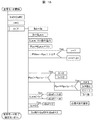
- FIG. 16 is a PAD diagram in the steady mode of the photovoltaic power generation system according to the present invention.
- the circuit configuration for realizing the operation of the PAD diagram may be any of FIGS.
- the detection mode algorithm in the present embodiment the algorithm of the PAD diagram shown in FIG. 6 is suitable.
- the current Ib detected the last time is set to Ibb, and the last detected current ILave is set to Ib. Thereafter, ILave and Vin are taken in, ILave ⁇ Vin is calculated, and this is defined as Ppv. Then, the absolute value of PMax-Ppv is calculated using PMax, which is the maximum power obtained in the previous detection mode. If
- is greater than a predetermined ⁇ P, the solar radiation abrupt change is set to t T, The steady mode is terminated and the mode is changed to the detection mode.
- is smaller than a predetermined ⁇ P, t is set to t + ⁇ t, and the next processing is started.
- the maximum power point is detected in the detection mode shown in FIG. 6, and in the steady mode, a sudden change in solar radiation is detected and the detection mode is changed, and the hill-climbing method is performed with the maximum power point as an initial value.
- the maximum power follow-up control is performed.
- two different maximum power detection methods are provided in the detection mode and the steady mode, and the following effects are obtained.
- the frequency of the detection mode can be lowered by using the hill-climbing method together, and the decrease in the MPPT efficiency can be prevented.
- Another maximum power tracking method may be used in addition to the hill climbing method.
- the present invention can be applied to a photovoltaic power generation system linked to a commercial system for home use. Further, the present invention can be applied to a large-scale photovoltaic power generation system such as a solar power generation system such as a DC power supply system that is not connected to the grid, a solar cell system for remote islands and mountain huts, a solar cell system for smart grids, and a mega solar system.
- a solar power generation system such as a DC power supply system that is not connected to the grid
- a solar cell system for remote islands and mountain huts such as a solar cell system for remote islands and mountain huts
- a solar cell system for smart grids such as a mega solar system.
Landscapes
- Engineering & Computer Science (AREA)
- Life Sciences & Earth Sciences (AREA)
- Sustainable Development (AREA)
- Sustainable Energy (AREA)
- Power Engineering (AREA)
- Physics & Mathematics (AREA)
- Electromagnetism (AREA)
- General Physics & Mathematics (AREA)
- Radar, Positioning & Navigation (AREA)
- Automation & Control Theory (AREA)
- Control Of Electrical Variables (AREA)
- Dc-Dc Converters (AREA)
Abstract
太陽光発電システムにおいて、MPPT効率の向上が課題となっており、山登り法の他様々な提案がなされている。瞬時スキャン法はその時点の太陽電池の特性をスキャンするものでシンプルな制御かつ回路で実現できるため優れた方式であるがチョークコイルのインダクタンス値に制約が生じる恐れがあった。 太陽光発電システムにおいて、スイッチング素子を制御して太陽電池の電流を電流目標値とほぼ等しい値に制御する電流制御手段と、電流目標値を可変する目標値可変手段を具備し、電流目標値をゼロから徐々に増加させながらその都度電力を演算して電力が最大となる点の電流目標値を求める検出モードと、求めた電流目標値で動作する定常モードを持つシステムとした。
Description
本発明は、太陽電池の発電電力を電力変換装置を用いて変換して所望の電力を得るシステムに関し、特に太陽電池に接続された変換器を制御することによって、太陽電池の電力の最大点を検出するとともに、検出した最大電力点で変換器を動作させる最大電力追従制御法に関するものである。
図4は太陽電池の電流-電圧特性及び電流-電力特性を示すグラフである。
太陽電池の出力電圧Vpvと出力電流Ipvの特性は一般に図4の実線に示すような非線形の特性となる。すなわち、電圧-電流特性は、電圧Vpv=0において短絡電流Isc、開放電圧Vocにおいて電流Ipv=0となる特性である。電圧-電力特性は、電圧Vpmaxにおいて最大電力値Pmaxを有する。この最大電力点Pmaxのとき、Ipv=Ipmaxである。またこの電圧-電流特性や電圧-電力特性は日照条件や温度条件によって変化するため、太陽電池から効率よく電力を取り出すためには常にこの最大電力点を探索し、太陽電池に接続される電力変換器を制御して太陽電池の動作点が最大電力点となるように追従制御する必要がある。
最大電力追従制御法として一般によく知られた方法として、山登り法がある。この山登り法は、電力変換器の入力電圧指令値を微小変更し、これに応じて太陽電池の発電電力が増加するか減少するかを判定する。そして、この判定結果に依って次の電圧指令値を微小増加変更させるか微小減少変更させるかの変更方向を決定して指令値の微小変更を繰返す方法である。
あるいは、特許第4294346号公報に示された方法がある。この方法は、太陽電池の2端子にインダクタとスイッチング素子が直列に接続される構成の電力変換回路を有しており、最大電力点の検出時には、スイッチング素子をオン状態に保持させてインダクタを流れる電流をゼロから短絡電流まで変化させて、この時の電流-電圧特性をスキャンして最大電力点の電流,電圧を検出し、太陽電池の動作点がスキャンによって得られた最大電力点の電流,電圧となるように電力変換回路を動作させるものである。この方法は太陽電池の電流-電圧特性の全域を高速にスキャンできるため、山登り法よりも応答性が早く、また二山特性が発生した場合においても確実に最大電力点を検出して移動することが可能である。
上記山登り法は応答性が遅くなるという恐れがあった。また、太陽電池に部分影が発生した場合に生じる二山特性に対応できないという恐れがあった。
また、上記の特許文献1に示されたスキャン法は、太陽電池の電流Ipv-電圧Vpvの特性をスキャンする際に、スイッチング素子をオン状態に保つことにより、電力変換回路のチョークコイルLに流れる電流Ipvの変化率di/dtが、
di/dt=Vpv/L
となることを利用してIpvを変化させている。したがって、電流変化率di/dtはチョークコイルのインダクタンス値(L値)に反比例する。Ipvの変化を精度良くスキャンするためには電流変化率di/dtを適切な値に抑える必要があり、L値は下限値を持つ。このことから、チョークコイルは下限値以上のインダクタンス値が必要である。特許文献1のスキャン法はチョークコイルの体積の小型化と、検出精度とのトレードオフを改善することが困難である恐れがある。
di/dt=Vpv/L
となることを利用してIpvを変化させている。したがって、電流変化率di/dtはチョークコイルのインダクタンス値(L値)に反比例する。Ipvの変化を精度良くスキャンするためには電流変化率di/dtを適切な値に抑える必要があり、L値は下限値を持つ。このことから、チョークコイルは下限値以上のインダクタンス値が必要である。特許文献1のスキャン法はチョークコイルの体積の小型化と、検出精度とのトレードオフを改善することが困難である恐れがある。
本発明が解決すべき課題は、応答性の向上と、部分影への対応と、太陽光発電システムにおける電力変換器のチョークコイルの体積の小型化および重量を低減し、低コスト化するとともに、最大電力点の検出精度を確保するこことによって、常に高いMPPT効率を持つ小型軽量かつ低コストな太陽光発電システムを実現することにある。
本発明は、太陽電池と、前記太陽電池に接続される電力変換器を有する太陽光発電システムにおいて、前記電力変換器は、少なくとも1個のスイッチング素子と、太陽電池から前記電力変換器に流入する電流を検出して入力電流を得る電流検出手段と、電流目標値と、前記電力変換器に入力される電圧を検出して入力電圧を得る電圧検出手段と、前記スイッチング素子をスイッチング制御することによって前記入力電流を前記電流目標値と略等しい値に制御する電流制御手段と、前記電流目標値を可変する目標値可変手段とを具備するとともに、前記目標値可変手段により前記電流目標値を略ゼロから順次増加させながら前記電流制御手段を動作させ、その都度前記入力電流と前記入力電圧からその時点の電力を演算するとともに、前記電力が最大となる点の電流目標値を求める検出モードと、前記検出モードにより求めた前記電流目標値を用いて前記電流制御手段を動作させる定常モードを有することを特徴とする。なお、前記検出モードにあっては一定時間の経過後に前記定常モードに遷移してもよいし、前記入力電圧が所定の値以下に低下すると前記定常モードに遷移させても良い。また、前記定常モードから前記検出モードへの遷移は一定時間毎に行うことや、その際、前記定常モードの電力が、前記検出モードで検出した最大電力に対して予め定めた割合以上に変動した場合には前記一定時間の経過を待たず検出モードに遷移することも有効である。
前記検出モードにおける前記目標値可変手段の可変方法は、前回の定常モードで用いた電流目標値に比べ所定の値だけ少ない電流値を超過した後、前記電流目標値の増加率をそれまでの増加率よりも緩やかにさせることや、前回の定常モードの電流目標値を基準とする所定の幅の内側にあっては前記目標値可変手段の増加率を前記所定の幅の外側に比べて緩やかにしても良い。
さらに、前記電力変換器を複数有しており、そのうちの1つの電力変換器が検出モードにある場合には、他の電力変換器は定常モードにすることや、一回の前記定常モードの動作時間をT、前記電力変換器の並列台数をnとすると、各電力変換器は、T/nずつ遅れて定常モードから検出モードに遷移することも有効な手段である。
あるいは、前記太陽光システムの起動時において、複数回検出モードと定常モードとを繰り返すとともに、前記複数回の検出モードにおける電流目標値可変手段の電流増加率は前回よりも高くしながら前記検出モードで得られた最大電力値と、その直後の定常モードで得られた最大電力値との誤差が所定の値以下でかつ電流目標値可変手段の電流増加率ができるだけ大きい条件を選定し、選定した電流増加率を以後の検出モードにおける電流目標値可変手段の電流増加率として用いても良い。
前記電力変換器は昇降圧コンバータの機能を有するとともに、検出モードにおいては電流目標値の増加とともに降圧動作から昇圧動作に遷移させても良いし、定常モードにおいては、直前の検出モードで求めた電流目標値を初期値として、前記電流目標値を微小増加あるいは微小減少させ、その結果変化した入力電圧と電流から電力の増減を判定するとともに、前記電力がより大きくなる方向に前記電流目標値を微小変更してもよい。
太陽電池と電力変換器と商用系統が接続される太陽光発電システムであって、前記電力変換器は前記太陽電池の最大電力を検出する検出モードと定常モードを有し、前記検出モードにおいても前記太陽電池の電力を前記電力変換器から前記商用系統に出力する機能を有することによっても本発明の課題を解決することが可能である。
あるいは、本発明は、太陽電池が最大電力点で動作するように追従制御する電力変換器において、前記太陽電池の最大電力点を検出する場合に、前記太陽電池の電流を制御するための電流目標値を、一旦所定の電流値にした後に、前記所定の電流値から短絡電流に至るまで所定の電流幅ごとに変化させながら、前記太陽電池の電力をサンプリングし前記最大電力点を検出することを特徴とする。
あるいは、本発明は、太陽電池が最大電力点で動作するように追従制御する電力変換器において、前記太陽電池の最大電力点を検出する場合に、前記太陽電池の電流を制御するための電流目標値を一旦所定の電流値にした後に、前記太陽電池の電圧が所定の電圧に至るまで前記電流目標値を所定の電流幅ごとに変化させながら、前記太陽電池の電力をサンプリングし前記最大電力点を検出することを特徴とする。
あるいは、太陽電池の出力電流と出力電圧から前記太陽電池の最大電力点を検出する検出制御モードと、定常制御モードからなる前記太陽電池の最大電力点追従制御方法において、前記検出制御モードは電流目標値を定める目標値設定ステップと、前記出力電流を前記電流目標値と略等しい値に制御する電流制御ステップと、前記出力電流と前記出力電圧を検出する電流・電圧検出ステップと、前記出力電流と前記出力電圧との乗算からなる電力とそのときの出力電流とを記憶する電力・電流記憶ステップと、からなり、前記目標値設定ステップでは前記電流目標値は徐々に増加し、前記電力・電流記憶ステップでは前回の電力・電流記憶ステップにて記憶した電力と今回の電力とを比べ、大きいほうの電力とそのときの出力電流を記憶していき、前記検出制御モードは所定時間経過後に前記定常制御モードへ遷移し、前記定常制御モードでは前記電力・電流記憶ステップにおいて記憶した電力である最大電力点に従い太陽電池の出力電流と出力電圧とを制御することを特徴とする。
あるいは、本発明は、太陽電池の出力電流と出力電圧から前記太陽電池の最大電力点を検出する検出制御モードと、定常制御モードからなる前記太陽電池の最大電力点追従制御方法において、前記検出制御モードは電流目標値を定める目標値設定ステップと、前記出力電流を前記電流目標値と略等しい値に制御する電流制御ステップと、前記出力電流と前記出力電圧を検出する電流・電圧検出ステップと、前記出力電流と前記出力電圧との乗算からなる電力とそのときの出力電流とを記憶する電力・電流記憶ステップと、からなり、前記目標値設定ステップでは前記電流目標値は徐々に増加し、前記電力・電流記憶ステップでは前回の電力・電流記憶ステップにて記憶した電力と今回の電力とを比べ、大きいほうの電力とそのときの出力電流を記憶していき、前記検出制御モードは前記電流・電圧検出ステップにおいて検出された電圧が所定の値になった際に終了し前記定常制御モードへ遷移し、前記定常制御モードでは前記電力・電流記憶ステップにおいて記憶した電力である最大電力点に従い太陽電池の出力電流と出力電圧とを制御することを特徴とする。
あるいは、本発明は、太陽電池の出力電流と出力電圧から前記太陽電池の最大電力点を検出する検出制御モードと、定常制御モードからなる前記太陽電池の最大電力点追従制御方法において、前記検出制御モードは電流目標値を定める目標値設定ステップと、前記出力電流を前記電流目標値と略等しい値に制御する電流制御ステップと、前記出力電流と前記出力電圧を検出する電流・電圧検出ステップと、前記出力電流と前記出力電圧との乗算からなる電力とそのときの出力電流とを記憶する電力・電流記憶ステップと、からなり、前記目標値設定ステップでは前記電流目標値は徐々に増加し、前記検出制御モードは前記電流・電圧検出ステップにおいて検出された電圧が所定の値になった際に終了し前記定常制御モードへ遷移し、前記定常制御モードでは前記電力・電流記憶ステップにおいて記憶した電力の内、最大電力となる最大電力点に従い太陽電池の出力電流と出力電圧とを制御することを特徴とする。
あるいは、本発明は、太陽電池の出力電圧と出力電流を検出するステップと、前記出力電流の目標値を定めるステップと、前記出力電流を前記目標値と略等しい値に制御するステップと、前記出力電流と前記出力電圧の乗算からなる電力とそのときの出力電流を記憶するステップとからなり、前記目標値を定めるステップでは目標値は徐々に増加し、前記記憶するステップでは前回の電力・電流記憶ステップにて記憶した電力と今回の電力とを比べ、大きいほうの電力とそのときの出力電流を記憶していくことを特徴とする。
本発明では電流の時間変化率はチョークコイルのインダクタンス値には依存せず、設定する電流目標値の増加率に依存する。このため、最大電力点の検出精度や、従来のスキャン法が持つ太陽電池特性の温度変化,経時変化や部分影発生時などに対する優れた対応性を確保したまま、チョークコイルのインダクタンス値を自由に選定することが可能になる。
したがって、本発明によれば、太陽光発電システムにおける電力変換器のチョークコイルのインダクタンス値は、スイッチング素子やダイオードのスピード,スイッチング損失,出力側のリプル電流などから決まる最適なスイッチング周波数を勘案して選定することができる。このため、高速なスイッチング素子を使うことによってチョークコイルのインダクタンス値を従来よりも低減することができる。この結果、チョークコイルの体積の小型化およびチョークコイルの重量を低減することができる。チョークコイルを低インダクタンス化すると、チョークコイルの材料である銅線の長さを短くでき、またフェライト材で構成されるコア体積も低減できる。この結果、チョークコイルは小型かつ軽量になり、かつ低コスト化することもできる。低インダクタンスなチョークコイルは基板搭載が可能となり、パワーコンディショナ製造時の工数削減にも寄与する。
この結果として、本発明によれば、常に高いMPPT効率を持ち、かつ小型軽量かつ低コストな太陽光発電システムを実現することができる。
本発明では、小型軽量かつ低コストな太陽光発電システムの実現に貢献するため、下記の構成を提案する。
本発明の第1の実施例を図1と図2,図3,図4を用いて説明する。
図1は、本発明の実施例1の回路構成を示す図である。まず、図1において、1は太陽電池パネル、2はパワーコンディショナ、3は商用系統、4は入力フィルタ、7はDC-DCコンバータ、8はチョークコイル、9はパワーMOSFET、10は昇圧ダイオード、11はコンデンサ、12は系統連系インバータ、13は電流センサ、14は制御回路、15a,15bは分圧抵抗、16は目標値可変手段、17はモード切替器、18は減算器、19はPI制御ブロック、20は乗算器、21a,21bはAD変換器、22aはPWM回路、23は最大値判定回路である。
図1において、パワーコンディショナ2の内部には入力フィルタ4とDC-DCコンバータ7,系統連系インバータ12,制御回路14がある。太陽電池パネル1はその両端がパワーコンディショナ2の内部の入力フィルタ4の入力側端子に接続されており、入力フィルタ4のコンバータ側端子はDC-DCコンバータ7に接続され、DC-DCコンバータ7は系統連系インバータ12に接続されている。系統連系インバータ12はパワーコンディショナ2の外部の商用系統3に接続されている。DC-DCコンバータ7の内部には、チョークコイル8,分圧抵抗15a,15b,パワーMOSFET9,昇圧ダイオード10,コンデンサ11、それに電流センサ13があり、チョークコイル8とパワーMOSFET9のドレインが接続されている。チョークコイル8の入力側は、入力フィルタ4のコンバータ側端子と接続される。また、パワーMOSFET9のソースは入力フィルタ4のコンバータ側端子に接続される。入力フィルタ4のコンバータ側端子の両端で、DC-DCコンバータ7の内部側には分圧抵抗15a,15bが直列に接続されている。パワーMOSFET9のドレインには昇圧ダイオード10のアノードが接続される。昇圧ダイオード10のカソードとパワーMOSFET9のソースの間にコンデンサ11が接続される。コンデンサ11の両端はDC-DCコンバータ7の外部にある系統連系インバータ12に接続される。
一方、制御回路14の内部にはAD変換器21a,21b,目標値可変手段16,モード切替器17,減算器18,PI制御ブロック19,乗算器20,PWM回路22a,最大値判定回路23がある。
分圧抵抗15a,15bの中点からAD変換器21aに接続される。電流センサ13はAD変換器21bに接続される。チョークコイル8を流れる電流をILとすると、AD変換器21bの出力はILの平均値であるILave、AD変換器21aの出力はVinである。ILaveとVinは乗算器20に入力され、出力はPpvとして最大値判定回路23に入力される。また、ILaveは減算器18のマイナス側端子に入力される。減算器18のプラス側入力端子にはモード切替器17の出力であるIrefが接続される。減算器18の出力はPI制御ブロック19に入力される。また、Irefは最大値判定回路23に入力される。PI制御ブロック19の出力は、PWM回路22aに入力される。PWM回路22aの出力はS1制御信号として制御回路14の外部に出力されDC-DCコンバータ7の内部のパワーMOSFET9のゲートに接続される。また、最大値判定回路23の出力はIrefMとしてモード切替器17の定常側に接続される。モード切替器17の検出側には目標値可変手段16が接続される。ここで、電流目標値Irefとは、モード切替器17から出力されるものであり、チョークコイル8を流れる電流ILの目標値である。
次に、図2を説明する。図2は実施例1の回路動作を示しており、横軸を時間として、図1の回路各部の動作波形を示した図である。上から順に、DC-DCコンバータ7の動作状態として定常モードと検出モードの区別、Vpvとして図1の太陽電池パネル1の両端の定常モードと検出モード時の電圧波形、電流目標値Iref,S1制御信号としてパワーMOSFET9のゲート波形、実線はIL、点線はILave、DC-DCコンバータ7出力電力としてDC-DCコンバータ7から系統連系インバータに出力される電力を示す。ここで、検出モードとは、太陽電池の最大電力点を検出するモードのことであり、定常モードとは、検出モードで得た最大電力点の電流となるように電力変換器(パワーコンディショナ2)を動作させるモードのことである。
次に図3は、図1における入力フィルタ4の内部の一例を示した図である。図3において、5a,5bはコモンモードチョーク、6a,6b,6c,6d、6eはフィルタコンデンサ、27はノーマルモードチョークである。図3において、入力フィルタ4の入力側端子の両端にはフィルタコンデンサ6aが接続され、フィルタコンデンサ6aの両端にはコモンモードチョーク5aの入力側端子が接続される。コモンモードチョーク5aの出力側端子はフィルタコンデンサ6bと6cの直列体に接続される。フィルタコンデンサ6bと6cの中点はフレームグランドに接続される。フィルタコンデンサ6bと6cの直列体の両端にはフィルタコンデンサ6dの両端が接続される。フィルタコンデンサ6dの両端はコモンモードチョーク5bの入力側端子が接続される。コモンモードチョーク5bの出力側端子の一方にはノーマルモードチョーク27が接続され、ノーマルモードチョーク27とコモンモードチョーク5bの他方の端子の間にフィルタコンデンサ6eが接続される。そして、フィルタコンデンサ6eの両端子はコンバータ側端子となり入力フィルタ4の外部に引き出される。
次に図4は、太陽電池の電流-電圧特性、および電流-電力特性を示すグラフであり、横軸を太陽電池パネル1の電流Ipv、縦軸を電圧Vpv(左側)と電力Ppv(右側)として、実線で太陽電池パネル1の出力電流Ipvと電圧Vpvの特性を示す。一方、点線は太陽電池パネル1の出力電流Ipvと電力Ppvの特性を示す。
続いて動作を説明する。定常モードにおいては、図1におけるモード切替器17は定常モード側に接続されている。そのため、電流目標値Irefは最大値判定回路23の出力であるIrefMとなる。本実施例において、図2中の検出モード手前の定常モードの期間におけるIrefMをIrefM(n-1)、図2中の検出モード以降の定常モードの期間におけるIrefMをIrefM(n)と定義する。そこで、現時点が図2の検出モードの手前の定常モードであるとすると、電流目標値はIrefM(n-1)である。このとき、本発明においては、DC-DCコンバータ7はチョークコイル8(L)に流れる電流の平均値ILaveがIrefM(n-1)と一致するように電流制御動作を行う。DC-DCコンバータ7では、チョークコイル8(L)に流れる電流を電流センサ13で検出する。チョークコイル8(L)に流れる電流ILは後述するパワーMOSFET9のスイッチングにより脈動するため、電流センサ13で検出された電流ILはAD変換器21bを経て制御回路14に取り込まれ平均値ILaveとして認識される。脈動する電流ILから平均値ILaveを取り出す方法としては、電流センサ13の内部にパワーMOSFET9(S1)のスイッチング周波数成分を減衰させる一次遅れフィルタを設ける方法や、AD変換器21aの取り込みタイミングをPWM周期と同期させて常に脈動の中心値をサンプリングする方法などがあり、脈動する電流ILから平均値ILaveを取り出すことができればいずれの方法を用いても良い。さて、このILaveは減算器18において、電流目標値Irefから差し引かれるが、このときIref=IrefM(n-1)であるため、減算器18の出力である電流誤差はIrefM(n-1)-ILaveとなる。この電流誤差はPI制御ブロック19に入力され、比例積分演算される。このPI制御ブロック19の出力は時比率であり、この時比率はPWM回路22aに入力されPWMパルスを生成する。このPWMパルスはS1制御信号であり、図2に示されるようなパルス波形である。S1制御信号はパワーMOSFET9(S1)のゲートに入力され、パワーMOSFET9(S1)を駆動する。パワーMOSFET9(S1)はスイッチングによりON/OFFを繰り返す。パワーMOSFET9(S1)がONした際には太陽電池パネル1-入力フィルタ4-チョークコイル8(L)-パワーMOSFET9(S1)-入力フィルタ4-太陽電池パネル1の閉回路が形成され、太陽電池パネル1からチョークコイル8(L)に電流が流れる。次にパワーMOSFET9(S1)がOFFすると、太陽電池パネル1-入力フィルタ4-チョークコイル8(L)-昇圧ダイオード10(D1)-コンデンサ11(Cpn)-入力フィルタ4-太陽電池パネル1の回路が形成され、チョークコイル8(L)に蓄えられた励磁エネルギーはコンデンサ11(Cpn)に放出される。
電流誤差IrefM(n-1)-ILaveが正の場合にはS1制御信号のON幅が増大してチョークコイル8(L)に蓄える励磁エネルギーを増加させ、反対に電流誤差IrefM(n-1)-ILaveが負の場合にはS1制御信号のON幅を縮小させてチョークコイル8(L)に蓄える励磁エネルギーを減少させる。この動作を繰り返すことにより、電流誤差IrefM(n-1)-ILaveをゼロに、言い換えればILaveがIrefM(n-1)と等しくなるように制御する。このとき、図2の定常モードではILaveは点線で示すようにIrefM(n-1)と等しい一定値となり、ILの波形は実線で示すようにパワーMOSFET9(S1)がONしている期間に増加し、パワーMOSFET9(S1)がOFFしている期間に減少する。そしてILave波形はIL波形の中央部を通る。
パワーMOSFET9(S1)がONするとチョークコイル8(L)に励磁エネルギーが蓄えられていきILは増加し、パワーMOSFET9(S1)がOFFとなるとチョークコイル8(L)に蓄えられた励磁エネルギーはコンデンサ11(Cpn)に放出されILは減少する。
ここで、電流誤差IrefM(n-1)-ILaveをゼロにするような制御に限るものでなく、ゼロに近い値となるよう制御しても良い。
このとき、図3の入力フィルタ4では主にノーマルモードチョーク27とフィルタコンデンサ5eにより、パワーMOSFET9(S1)のスイッチングによるILの脈動成分がカットされ、太陽電池パネル1からDC-DCコンバータ7に流入する電流Ipvは、ほぼILaveと同じ直流値となる。一方、電圧に関しては、入力フィルタ4に入力される太陽電池パネル1の電圧Vpvと入力フィルタ4の出力電圧Vinは、DC成分はほぼ等しく、Vinにはスイッチングに伴う高周波成分が含まれる。
この結果、太陽電池パネル1からDC-DCコンバータ7にはIpvかつVpvの直流電力が流入し、DC-DCコンバータ7から系統連系インバータ12にはDC-DCコンバータ7の損失を差し引いただけの電力が出力される。系統連系インバータ12においては、DC-DCコンバータ7から入力された直流電力を、商用系統3の電圧位相に同期した正弦波電流に変換して商用系統3に出力する。
次に検出モードについて説明する。本実施の形態では、定常モードにおいて一定時間経過すると検出モードに遷移する。検出モードは図1におけるモード切替器17を検出モード側に切り替えることにより開始される。このとき、目標値可変手段16の初期値はゼロに設定されている。そのため、モード切替器17を検出モードに切り替えるとIrefはそれまでの定常モード時のIrefM(n-1)からゼロとなる。チョークコイル8(L)を流れる電流の平均値ILaveは、それまでの定常モードと変わらず、減算器18において、電流目標値Irefから差し引かれるが、検出モードの最初はIref=0であるため、減算器18の出力である電流誤差は-ILaveとなる。この電流誤差はPI制御ブロック19に入力され、比例積分演算される。このPI制御ブロック19の出力は時比率であり、この時比率はPWM回路22aに入力されPWMパルスを生成する。このPWMパルスはS1制御信号であり、図2に示されるようなパルス波形である。S1制御信号はパワーMOSFET9(S1)のゲートに入力され、パワーMOSFET9(S1)を駆動する。パワーMOSFET9(S1)がONするとチョークコイル8(L)に励磁エネルギーが蓄えられるとともにILは増加し、パワーMOSFET9(S1)がOFFとなるとチョークコイル8(L)に蓄えられた励磁エネルギーはコンデンサ11(Cpn)に放出されILは減少する。この結果、DC-DCコンバータ7は電流誤差である-ILaveがゼロになるように電流制御される。この結果、チョークコイル8(L)に流れる電流の平均値ILaveはゼロとなり、太陽電池パネル1から出力される電流Ipvもゼロとなる。このとき、太陽電池パネル1の電圧は図4の電流-電圧特性に示すように、Ipvがゼロの時に開放電圧Vocまで上昇する。この変化は図2にも示されており、ILave、すなわちILの平均値(点線)がゼロに低下するとともに、VpvがVocまで上昇する。なお、このときIrefをゼロに変更する代わりに検出モードの最初に一定時間だけパワーMOSFET9のスイッチングを止める方法をとっても良い。次に、図2に示すように電流目標値Irefを傾きdi/dtでゼロから徐々に上昇させる。この操作は、図1に示すように目標値可変手段16から出力する電流目標値Irefを所定時間tx毎に微小量ΔIrefずつ増加することによって達成される。Irefはdi/dt=ΔIref/txの傾きで増加する。このとき検出モードの最初にパワーMOSFET9のスイッチングを止めた場合はスイッチングを再開する。これにともない、図2に示すように、ILaveがIrefにほぼ等しい状態を保つため、Irefの上昇に追従してILが上昇する。このときも前述のように入力フィルタ4の働きによりIpvはほぼILaveに等しいため、検出モードにおいてはIpvがゼロから徐々に増加することになる。VpvはIpvの変化により図4に示す実線の特性に従い変化する。このとき、ILaveとVinをその都度AD変換器21aと21bでサンプリングされる。サンプリング周期tsはIrefが変化する時間txよりも短い。検出したILaveとVinはそれぞれIpv,Vpvとみなすことができるので、これらを検出して乗算器20でPpvを算出することにより、最大値判定回路23では、Ppvとその時のIrefを(Ppv,Iref)の組として把握することができる。最大値判定回路23では、順次入力される(Ppv,Iref)の組のうちでPpvがそれまでよりも大きな場合にPpvを最大電力点PMaxとし、その時のIrefをIrefMとして記憶する。Irefはdi/dt=ΔIref/txの傾きで増加するため、tx*Isc/ΔIrefの時間で図4に示す短絡電流値Iscに達する。この電流Ipvの増加に伴って、電圧VpvはVocから徐々に低下して短絡電流値IscのときVpv=0となる。この間に、最大電力点である(Pmax,Ipmax)の点を通るため、最大値判定回路23にはIref=Iscの時点で、(PMax,IrefM)=(Pmax,Ipmax)が記憶されていることになる。本実施の形態においては図2に示すように検出モードはTsの期間実行し、
tx*Isc/ΔIref<Ts
としているため、Tsまでに電流目標値IrefはIsc以上に達する。IrefがIsc以上になった場合には、ILave<IrefとなってILをIrefに追従させる電流制御ができなくなるが、このときパワーMOSFET9はPWM回路22aで予め設定されている最大オン時間幅で動作する。
tx*Isc/ΔIref<Ts
としているため、Tsまでに電流目標値IrefはIsc以上に達する。IrefがIsc以上になった場合には、ILave<IrefとなってILをIrefに追従させる電流制御ができなくなるが、このときパワーMOSFET9はPWM回路22aで予め設定されている最大オン時間幅で動作する。
この結果、検出モードの終了時点、すなわち検出モード開始から時間Tsが経過した時刻において、最大値判定回路23には(PMax,IrefM)として(Pmax,Ipmax)が記憶されていることになる。
そこで、次の定常モードにおいては、最大値判定回路23からはIrefMとしてIpmaxを出力する。定常モードにおいては前述したようにモード切替器17は再び定常側に接続され、Iref=IrefM(n)=Ipmaxとし、ILの平均値ILaveがIpmaxとなるように電流制御する。なお、定常モードの時間はこれをTとすると、検出モードの時間Tsに比べて十分に長い時間とする。例えば、検出モードの時間Tsは1ms~数10msのオーダー、定常モードの時間Tは1s~数分のオーダーである。また、このときに使用するチョークコイル8のインダクタンス値は概ね100μH~1mHの間の値であり、プリント基板上に搭載可能である。
本実施例において、検出モード時のdi/dtはチョークコイル8のインダクタンス値に依存するものではなく、設定する電流目標値の増加率に依存するものであるため、チョークコイルのインダクタンス値を自由に選定することが可能となり、小型軽量かつ低コストな太陽光発電システムを実現することができる。
このようにして、本実施例では太陽電池パネルの最大電力点を所定時間毎に検出し、パワーコンディショナを検出した最大電力点で動作させることができる。本発明においては図2に示したように、検出モードにおいても太陽電池パネル1の電力はDC-DCコンバータ7から出力され系統連系インバータ12を経て商用系統3側に出力される。このため、検出精度を向上させるためにdi/dtを小さく、すなわち電流変化の増加率を緩くして検出モードに時間を掛けても太陽電池パネルからの電力の損失は最小限に抑えることができる。
なお、本実施例において、PWM回路22aとパワーMOSFET9の間にゲートドライブ回路を用いることも有効である。パワーMOSFET9をIGBTやSiC-MOSFETなど他のスイッチング素子に置き換えても良い。昇圧ダイオード10にSiCデバイスを適用することも効果的である。DC-DCコンバータ7の構成は図1に示した昇圧型コンバータが好ましいが、その他の非絶縁型コンバータや絶縁型コンバータであってもよい。また、入力フィルタ4は同様の機能、すなわちスイッチング成分の電流が太陽電池パネル側に流れるのを防止するとともに、コモンモードノイズを低減する役割の回路構成であれば他の構成としても良い。また、制御回路は同様の機能を持つアナログ回路で構成しても良い。PWM回路22aはパルス幅変調制御を行う回路であるが、これはパルス周波数変調制御(PFM)やパルス密度変調制御(PDM)などで置き換えることもできる。さらに、PI制御ブロック19は比例積分制御を行うブロックであるが、前述のようにオペアンプなどのアナログ回路で構成しても良いし、PID(比例積分遅延)制御等に置き換えても良い。
また、本実施例において、目標値可変手段16の初期値をゼロとしたが、この限りではない。目標値可変手段16の初期値をゼロとするのは最大電力点を検出する際のサンプリングにおいて漏れがないようにするという意味も持っているためである。よって、目標値可変手段16の初期値はゼロに限るものではなく、ゼロに近い値としても良い。
また、定常モードから検出モードに遷移する時に目標値可変手段16の値を目標値可変手段16の値を徐々に低減させてゼロ、あるいはゼロに近い値に変更してもよい。目標値可変手段16の値を徐々に低減させることで、太陽電池パネル1とパワーコンディショナ2の間のケーブルの寄生インダクタンスによる電圧跳ね上がりを防止することができる。
また、電流目標値Irefをゼロあるいはゼロに近い値から徐々に上昇させていくタイミングはILaveがゼロあるいはゼロに近い値となっている場合を検出したときでも、一定の時間が経過したときでも、一定のスイッチング回数をカウントしたときでも良い。
また、本実施例において、最大値判定回路23では、順次入力される(Ppv,Iref)の組のうちでPpvがそれまでよりも大きな場合にPpvを最大電力点PMaxとし、その時のIrefをIrefMとして記憶しているが、この限りでない。最大電力点PMaxが分かればよいため、最大値判定回路23にて順次入力される(Ppv,Iref)の組を全て記憶しておき、記憶した中で最も大きなPpvを最大電力点PMaxとしても良い。この場合、最大電力点PMaxのときのIrefがIrefMとされ、その後の定常モードはIrefMとしてIpmaxを出力する上記の動作の通りである。
また、本実施例においては一定時間経過により定常モードから検出モードへ遷移しているが、この限りではない。定常モードから検出モードへ遷移するタイミングが設けられれば良く、スイッチング回数などの所定の条件下で遷移しても良い。
また、本実施例においては一定時間経過により検出モードから定常モードへ遷移しているが、この限りではない。検出モードから定常モードへの遷移は、検出モードが終了した段階や最大電力点が検出された段階で行われればよく、スイッチング回数などの所定の条件下で遷移しても良い。
また、本実施例においては目標値可変手段16において目標電流値を定めていったがこの限りではない。電流値ではなく電圧値でも良い。
また、本実施例では増加量ΔIrefを微小量としているがこの限りでない。
次に、本発明の第2の実施例を図5,図6,図7および図8を用いて説明する。図5は本発明の回路構成を示した図であり、前述した図1と同じ構成要素には同じ記号を付与している。その他、図5において、28は制御ブロックである。
図5は本発明の実施例2の回路構成を示す図である。
図5における回路構成要素の接続形態は、前記実施例1において図1を用いて説明した形態と大半が同じであるため、以下には異なる点のみ記載する。
制御回路14の内部にはAD変換器21a,21b,減算器18,PI制御ブロック19,PWM回路22a,制御ブロック28がある。そして、分圧抵抗15a,15bの中点からAD変換器21aに接続される。電流センサ13はAD変換器21bに接続される。AD変換器21bの出力はILの平均値であるILaveであり、一方のAD変換器21aの出力はVinである。ILaveとVinは制御ブロック28に入力されて情報処理される。制御ブロック28の出力はIrefであり、減算器18のプラス側入力端子に接続される。また、ILaveは減算器18のマイナス側端子にも入力される。減算器18の出力はPI制御ブロック19に入力される。PI制御ブロック19の出力は、PWM回路22aに入力される。PWM回路22aの出力はS1制御信号として制御回路14の外部に出力されDC-DCコンバータ7の内部のパワーMOSFET9のゲートに接続される。
図6は本発明の実施例2の制御アルゴリズムのうち検出モードを示すPAD図であり、図7は本発明の実施例2の制御アルゴリズムのうち定常モードを示すPAD図である。
図6は図5の制御ブロック28の内部の処理内容を表したPAD図であり、そのうち検出モードの処理内容を示している。
一方、図7は同じ制御ブロック28の処理内容を表すPAD図であり、定常モードの処理内容を示している。
図8は本実施例における各部の動作波形を示した図である。
次に本実施例における動作を説明する。図5において、DC-DCコンバータ7の動作は前述の実施例1と同様であるため、主に制御ブロック28に関連する内容について詳述する。
図5においては、検出モード,定常モードによらず、AD変換器21b,21aによりそれぞれL電流平均値ILaveと入力電圧Vinがディジタル信号に変換され制御ブロック28に入力され、制御ブロック28からはIrefが出力される。図6において、検出モードが開始されると、まずIref=0と設定され、制御ブロック28からはIref=0が出力される。制御回路14はマイコン、あるいはDSP(デジタルシグナルプロセッサ)を用いるのが好適である。制御回路14の内部ではAD変換器21bによりAD変換されたILaveと、0(=Iref)を比較し、PI制御ブロック19でILaveをゼロにするために必要なパワーMOSFET9(S1)の時比率を出力する。そしてPWM回路22aで時比率はパルス幅に変換され、S1制御信号としてパワーMOSFET9(S1)のゲートをスイッチング制御する。この電流フィードバック制御により、チョークコイルLを流れる電流の平均値ILaveはゼロまで低下する。PAD図ではこのILaveをサンプリング周期毎に取り込み、ILave>0の場合には繰り返しILaveを読み込み、ILave=0となった時、Vinを読み込む動作に移行する。
まず、PMax=0に設定する。
ここで、予めVminを設定する。Vminは0V以上の値であっても良い。そしてVin>Vminの時、すなわち太陽電池の端子間電圧VpvがVminに低下するまで次の操作を行う。その操作とは、電流目標値Irefを現在のIrefにΔIrefを加算し、ILaveとVinを読み込み、それらの積で電力Ppvを演算し、もしPpvがPMaxよりも大きい場合には、電力最大値PMaxを現在のPpvとし、同時にIrefMを現在のIrefとする。ここまでの操作を繰り返す。
そして、Vin≦Vminとなったら制御ブロック28の出力であるIrefとしてIrefMを出力する。ここまでの操作で検出モードは終了し、定常モードに移行する。検出モード終了判定は図8のPpv波形に示すように、VpvがVminを下回った点(○印)をもって行い、定常モードに遷移する。
次に、定常モードについてのPAD図は図7に示すとおりである。すなわち、制御ブロック28からの出力であるIrefをIref=IrefMとして、前述の検出モードで求めたIrefMを出力する。この定常モード開始時を時間t=0として、以下の繰り返し動作に入る。繰り返し動作の中では、ILaveとVinを読み込み、Ppv=ILave×Vinを演算する。そして、前回の検出モードで得られた最大電力PMaxを用いて、|PMax-Ppv|を演算する。この結果があらかじめ定めたΔP値を上回った場合には、t=Tとして繰り返しを中断し、検出モードに移行させる。一方、|PMax-Ppv|の演算結果がΔPよりも小さい場合には現在のtにΔtを加えた時間をtとする。そして、tがあらかじめ定めた定常モード時間であるTに達するまで、以上の動作を繰り返す。ここで、|PMax-Ppv|>ΔPが成立するときには日照の急変や影の発生など太陽電池パネル1の発電特性が前回の検出モードで計測した特性から急激に変わったことを示しており、このときには検出モードをやり直して新たな最大電力値を得ることで、高いMPPT効率を維持することができる。本実施例においては一定時間経過により定常モードから検出モードへ遷移しているが、これに限ったものではない。定常モードから検出モードへ遷移するタイミングが設けられれば良く、スイッチング回数などの所定の条件下で遷移しても良い。
実施例1と本実施例の大きな違いとして、定常モードにおいて電力の変動が大きい場合に検出モードに遷移させる点の他、前述した検出モードの終了を入力電圧すなわち太陽電池パネル1の電圧がゼロあるいはゼロ付近まで低下することで判断している点が挙げられる。このようなアルゴリズムをとることで、本実施例では検出モードから定常モードへの遷移を即座に移行することができるので、時間の損失が減少し、よりMPPT効率を向上させることが可能である。
また、本発明においては、Vminを設定することにより、太陽電池パネルの短絡電流に至る以前に検出を停止することができる。パワーコンディショナ駆動用の補助電源をVinから採取している場合にはVinをゼロに低下させるとパワーコンディショナが停止するため、補助電源が動作する最低電圧をVminに設定しておくことにより検出モードにおいて補助電源が停止する不具合が発生することはない。
なお、本実施例においても、PWM回路22aとパワーMOSFET9の間にゲートドライブ回路を用いることも有効である。パワーMOSFET9をIGBTやSiC-MOSFETなど他のスイッチング素子に置き換えても良い。昇圧ダイオード10にSiCデバイスを適用することも効果的である。DC-DCコンバータ7の構成は図5に示した昇圧型コンバータが好ましいが、その他の非絶縁型コンバータや絶縁型コンバータであってもよい。また、入力フィルタ4はスイッチング成分の電流が太陽電池パネル側に流れるのを防止するとともに、コモンモードノイズを低減する役割の回路構成であれば良い。また、制御回路14は同様の機能を持つアナログ回路で構成しても良い。制御回路14をマイコンあるいはDSPとし、AD変換器21a,21bをその外部に設置してディジタル変換した状態量を制御回路14に入力してもよい。PWM回路22aはパルス幅変調制御を行う回路であるが、これはパルス周波数変調制御(PFM)やパルス密度変調制御(PDM)などで置き換えることもできる。さらに、PI制御ブロック19は比例積分制御を行うブロックであるが、オペアンプなどのアナログ回路で構成しても良いし、PID(比例積分遅延)制御等に置き換えても良い。
次に、本発明の第3の実施例につき図9を用いて説明する。図9は本発明の検出モードにおける電流目標値の時間変化を示した図である。本実施例の電流変化パターンを図1の目標値可変手段16に適用することで以下の動作となり、新たな効果を得ることができる。
図9の上段はモード遷移、下段はモード遷移に応じた電流目標値の変化を示している。図9において横軸は時間である。図9において、前回の定常モードの電流目標値IrefはIrefM(n-1)である。検出モードではIrefは一旦ゼロとなり、図示のように電流変化の増加率aで時間とともに増加させる。そして、前回の定常時の電流目標値であるIrefM(n-1)からΔIだけ少ない電流値に達すると電流変化は増加率bとなる。増加率bはそれまでの増加率aよりも緩く、電流目標値Irefの傾き(di/dt)は緩くなるためIrefM(n-1)の付近では高い検出精度を得ることができる。一方、IrefM(n-1)よりも電流が十分小さい領域においては電流の時間変化を増加率aとすることにより検出モードの時間を短縮することができる。このように本実施例においては検出モードの時間短縮と検出精度の向上と言う相反する課題を解決することが可能である。
また、本実施例において、Irefは一旦ゼロとしたが、この限りではない。Irefの初期値を一旦ゼロとするのは最大電力点を検出する際のサンプリングにおいて漏れがないようにするという意味も持っているためである。よって、Irefの初期値はゼロでなくゼロに近い値としても良い。
本実施例では増加率aから増加率bに変わるタイミングは電流値が前回の定常時の電流目標値であるIrefM(n-1)からΔIだけ少ない電流値に達したときとしているがこの限りでない。検出モード時間短縮と検出精度の向上を目的としているため、一定時間経過により増加率を変えるなどの方法でも良い。
次に、本発明の第4の実施例につき図10を用いて説明する。図10は本発明の検出モードにおける電流目標値の時間変化を示した図である。本実施例の電流変化パターンを図1の目標値可変手段16に適用することで以下の動作となり、新たな効果を得ることができる。
図10の上段はモード遷移、下段はモード遷移に応じた電流目標値の変化を示している。図10において横軸は時間である。図10において、前回の定常モードの電流目標値IrefはIrefM(n-1)である。検出モードではIrefは一旦ゼロとなり、図示のように電流変化の増加率aで時間とともに増加させる。そして、前回の定常時の電流目標値であるIrefM(n-1)からΔIだけ少ない電流値に達すると電流変化は増加率bとなる。増加率bはそれまでの増加率aよりも緩く、電流目標値Irefの傾き(di/dt)は緩くなるためIrefM(n-1)の付近では高い検出精度を得ることができる。更に、電流Irefが増加しIrefM(n-1)からΔIだけ大きい電流値に達すると電流変化は増加率cとなる。増加率cは増加率bよりも急峻であり、増加率c=増加率aとしてもよい。
このように、IrefM(n-1)よりも電流が十分小さいか、十分大きい領域においては電流の時間変化を増加率a、あるいは増加率cとすることにより、検出モードの時間を短縮することができる。本実施例においては検出モードの時間短縮と検出精度の向上と言う相反する課題を解決することが可能である。
また、本実施例において、Irefは一旦ゼロとしたが、この限りではない。Irefの初期値を一旦ゼロとするのは最大電力点を検出する際のサンプリングにおいて漏れがないようにするという意味も持っているためである。よって、Irefの初期値はゼロでなくゼロに近い値としても良い。
本実施例では増加率aから増加率bに変わるタイミングは電流値が前回の定常時の電流目標値であるIrefM(n-1)からΔIだけ少ない電流値に達したときとしているがこの限りでない。検出モード時間短縮と検出精度の向上を目的としているため、一定時間経過により増加率を変えるなどの方法でも良い。増加率bから増加率cに変わるタイミングも同様である。
次に、本発明の第5の実施例につき図11と図12を使用して説明する。図11は本発明の第5の実施例における回路構成を示した回路ブロック図である。
図12は本発明の実施例5のモード遷移を示す図であり、本実施例のDC-DCコンバータの動作モードについて記載したシーケンスである。
図11において、前述の実施例における図1,図5と同じ構成要素には同じ記号を付与している。その他、図11において、1a,1bは太陽電池パネル、4a,4bは入力フィルタ、7a,7bはDC-DCコンバータである。
次に図11の構成を説明する。太陽電池パネル1a,1bはそれぞれパワーコンディショナ2の中の入力フィルタ4a,4bに接続される。入力フィルタ4a,4bはそれぞれDC-DCコンバータ7a,7bに接続される。DC-DCコンバータ7a,7bの出力は系統連系インバータ12に接続される。系統連系インバータ12はパワーコンディショナ2の外部の商用系統3に接続される。制御回路14a,14bはそれぞれDC-DCコンバータ7aおよび7bに接続される。
入力フィルタ4a,4bは図3に示した構成をとることが好ましいが、その他の構成でも良い。また、DC-DCコンバータ7a,7bの構成は図1に示した昇圧型コンバータが好ましいが、その他の非絶縁型コンバータや絶縁型コンバータであってもよい。
次に、本実施例の動作を説明する。制御回路14a,14bではそれぞれが接続されるDC-DCコンバータ7a,7bの動作状態を制御する。このとき、図12のモードが示すように、DC-DCコンバータ7aと7bは検出モードの時間Ts、定常モードの時間Tで動作するとともに、DC-DCコンバータ7aが検出モードに入ってから時間T/2経過後にDC-DCコンバータ7bが検出モードに遷移する。図示していないが、同様にDC-DCコンバータ7bが検出モードに入ってから時間T/2経過後にDC-DCコンバータ7aが検出モードに遷移する。Tsに対してTは十分に長い時間であるため、このように制御することによって2台のDC-DCコンバータ7aと7bは同時に検出モードに遷移せず、少なくとも一方のDC-DCコンバータは定常モードで動作する。
本実施例はN系列の太陽電池パネルがN台のDC-DCコンバータにそれぞれ接続されているケースに展開することができる。このケースにおいては、DC-DCコンバータ1~Nがあり、DC-DCコンバータ[n](1≦n≦N)はDC-DCコンバータ[n-1](ただしn=1のときはコンバータ[N])が検出モードに入ってから時間T/n経過後に検出モードに遷移する。
この動作により、DC-DCコンバータのうち1台ずつが検出モードに遷移することができる。検出モードにおいては、最大電力よりも出力が低下するが、DC-DCコンバータ群全体の出力電力は平均化され、系統連系インバータ12から商用系統には安定した電力を出力することが可能である。
また、本実施例においては一定時間経過により定常モードから検出モードへ遷移しているが、この限りではない。定常モードから検出モードへ遷移するタイミングが設けられれば良く、スイッチング回数などの所定の条件下で遷移しても良い。
また、本実施例においては一定時間経過により検出モードから定常モードへ遷移しているが、この限りではない。検出モードから定常モードへの遷移は、検出モードが終了した段階や最大電力点が検出された段階で行われればよく、スイッチング回数などの所定の条件下で遷移しても良い。
次に、本発明の第6の実施例である最適条件抽出法(オートチューニング)につき図13を用いて説明する。図13は本発明の起動時における電流目標値の時間変化を示した図である。本実施例の電流変化パターンを前述のそれぞれの実施例の起動時に適用することにより、新たな効果を得ることができる。
図13の上段はモード遷移、中段はモード遷移に応じた電流目標値の変化、下段はモード遷移に応じた電力値の変化を示している。図13の横軸は時間を示している。図13において、パワーコンディショナが起動すると、図示のように1回目の検出モードを開始する。第1回目の電流目標値Irefの時間変化は増加率aとして検出モードを実行し、電力最大値PMaxをとる電流目標値IrefMを求める。このとき求めた電力最大値をPMax(a)、電流目標値をIrefM(a)とする。続いてIrefM(a)を電流目標値として1回目の定常モードを開始する。定常モードを所定の時間だけ行い、このとき得られる電力Ppvを測定する。このPpvをPpv(a)とする。そして、
ΔP(a)=|PMax(a)-Ppv(a)|
の式によりΔP(a)を計算する。
ΔP(a)=|PMax(a)-Ppv(a)|
の式によりΔP(a)を計算する。
次に、電流目標値Irefの時間変化を増加率aよりも大きい増加率bとして2回目の検出モードを開始する。検出モードを実行し、電力最大値PMaxをとる電流目標値IrefMを求める。このとき求めた電力最大値をPMax(b)、電流目標値をIrefM(b)とする。続いてIrefM(b)を電流目標値として2回目の定常モードを開始する。定常モードを所定の時間だけ行い、このとき得られる電力Ppvを測定する。このPpvをPpv(b)とする。そして、
ΔP(b)=|PMax(b)-Ppv(b)|
の式によりΔP(b)を計算する。
ΔP(b)=|PMax(b)-Ppv(b)|
の式によりΔP(b)を計算する。
このようにしてn回、検出モードと定常モードを実施してΔP(1)~ΔP(n)を求める。そして、予め定めたΔPと比較し、このΔPよりも小さく、かつ増加率がもっとも大きい条件を求める。そして、求めた増加率を以降の検出モードにおける増加率として設定して動作させる。
太陽電池パネル1の応答特性や、太陽電池パネル1とパワーコンディショナ2の間のケーブル,入力フィルタ4,基板の配線などに含まれるインダクタンス分や容量分により、太陽電池のI-V特性は時定数を持つため、こうした応答特性の遅れを無視するためには、検出モードにおける電流目標値の増加率はできるだけ低い方が望ましい。また、増加率が低いほどサンプリング点数が増加するため最大電力点の検出精度も向上する。しかし一方で電流目標値の増加率が低いほど検出モードに費やす時間が増加し、最大電力点から外れた動作点で発電する時間が増加するためにMPPT効率が悪化するというトレードオフ特性がある。そこで、本実施例では上記の操作を行うことによって起動時に最適な増加率を求めることが可能になる。また、パワーコンディショナの認証試験においては実際の太陽電池パネルと異なる特性を持つ太陽電池模擬電源で評価試験をするケースもあり得る。太陽電池模擬電源の応答特性は太陽電池パネルと異なるため検出モードにおける電流目標値の増加率を低く設定する必要がある。その際にも本実施例の最適条件抽出法(オートチューニング)が有効に機能する。
次に、本発明の第7の実施例を図14と図15を用いて説明する。図14は本発明の第7の実施例の回路構成を表す回路図である。図15は本発明の実施例7の回路動作を示す各部波形である。
図14において、図1,図5,図11と同じ構成要素には同じ記号を付与している。その他、図14において、22bはPWM回路、24はパワーMOSFET、25はダイオード、26は信号処理回路である。図14の回路図の接続は大部分が図1の回路図と同じである。異なる部分について以下に説明する。入力フィルタ4のコンバータ側の正極側にはパワーMOSFET24(S2)のドレインが接続され、パワーMOSFET24(S2)のソースにはダイオード25(D2)のカソードが接続される。この接続点にチョークコイル8が接続される。ダイオード25(D2)のアノードは入力フィルタ4のコンバータ側の負極側に接続される。一方、制御回路14の内部においては、PI制御ブロック19の出力が信号処理回路26に接続され、信号処理回路26はPWM回路22a,22bに接続される。PWM回路22aはパワーMOSFET9(S1)のゲートに接続され、PWM回路22bはパワーMOSFET24(S2)のゲートに接続される。このように、図14はいわゆるHブリッジ型昇降圧コンバータの回路構成となっており、検出モードにおいて昇降圧動作を行うことが本実施例の特徴である。
次に、動作を説明する。図15に示すように、太陽電池パネル1の開放電圧Vocはコンデンサ11の電圧Vpnよりも高い。したがって定常モードから検出モードに遷移するとVpvは必ずVpnより高いVocまで上昇する。そこで、検出モードは昇圧モードから開始する。すなわち、Vpv>Vpnの時にはパワーMOSFET24(S2)をスイッチングし、パワーMOSFET9(S1)はオフ状態とし、降圧コンバータとして動作させる。このときにはパワーMOSFET24(S2)がオンすると、太陽電池パネル1-入力フィルタ4-パワーMOSFET24(S2)-チョークコイル8(L)-昇圧ダイオード10(D1)-コンデンサ11(Cpn)-入力フィルタ4-太陽電池パネル1の閉回路が形成され、チョークコイル8に電流が流れる。次にS2がオフすると、太陽電池パネル1側とチョークコイル8(L)とは切り離され、チョークコイル8(L)-昇圧ダイオード10(D1)-コンデンサ11(Cpn)-ダイオード25(D2)-チョークコイル8(L)の閉回路に電流が環流する。このとき、チョークコイル8(L)に流れる電流ILの平均値ILaveが電流目標値Irefになるように電流制御される。
Irefが増加するとともにVpvが低下するため、検出モードの途中でVpv>VpnからVpv<Vpnに変化する。そこで、Vpv<Vpnの時には、パワーMOSFET24(S2)をON状態とし、パワーMOSFET9(S1)をスイッチングして、昇圧コンバータとして動作させる。このときにはパワーMOSFET9(S1)がオンすると、太陽電池パネル1-入力フィルタ4-パワーMOSFET24(S2)-チョークコイル8(L)-パワーMOSFET9(S1)-入力フィルタ4-太陽電池パネル1の閉回路が形成され、チョークコイル8に電流が流れて励磁エネルギーが蓄積される。次にパワーMOSFET9(S1)がオフすると、太陽電池パネル1-入力フィルタ4-MOSFET24(S2)-チョークコイル8(L)-昇圧ダイオード10(D1)-コンデンサ11(Cpn)-入力フィルタ4-太陽電池パネル1の閉回路に電流が通流する。このときも、降圧コンバータ動作のときと同様に、チョークコイル8(L)に流れる電流ILの平均値ILaveが電流目標値Irefになるように電流制御される。
電流制御は、降圧モード,昇圧モードとも、ILを電流センサ13で検出し、AD変換器21bで取り込み、減算器18でIrefとの差分をとり、この差分をPI制御ブロック19で演算することによりパワーMOSFET24およびパワーMOSFET9の時比率を決定しパワーMOSFETをスイッチングする。このとき、信号処理回路26では次の処理を行う。まず、PI制御ブロックから入力される信号の下限を0、上限を2とすると、
信号処理回路26 入力信号:S_in 0≦S_in<2
S_S2=S_in ただし S_in>1のときS_S2=1
S_S1=S_in-1 ただし S_in<1のときS_S1=0
で制御する。信号S_S1,S_S2が0のときそれぞれ時比率はゼロである。また、信号S_S1,S_S2が1のとき、時比率は100%である。
信号処理回路26 入力信号:S_in 0≦S_in<2
S_S2=S_in ただし S_in>1のときS_S2=1
S_S1=S_in-1 ただし S_in<1のときS_S1=0
で制御する。信号S_S1,S_S2が0のときそれぞれ時比率はゼロである。また、信号S_S1,S_S2が1のとき、時比率は100%である。
上記のように制御することにより、昇圧モード,降圧モードによる動作切換をすることなく検出モードにおける太陽電池パネルの電圧が0からVocの広い範囲において電流制御を行うことができる。
次に、本発明の第8の実施例につき、図16を用いて説明する。図16は本発明による太陽光発電システムの定常モードにおけるPAD図である。このPAD図の動作を実現する回路構成は、図1,図5,図14のいずれでも良い。また、本実施例における検出モードのアルゴリズムとしては、図6に示すPAD図のアルゴリズムが好適である。
図16において、定常モードが開始されると、その前の検出モードで求めたIrefMを用いて、Iref=IrefMとして、t=0としてt<Tの範囲において、以下の処理を繰り返す。
繰り返す処理は、前々回検出した電流IbをIbbとし、前回検出電流ILaveをIbとする。その後、ILaveとVinを取り込み、ILave×Vinを演算してこれをPpvとする。そして、前回検出モードで求めた最大電力であるPMaxを用いてPMax-Ppvの絶対値を演算し、|PMax-Ppv|が予め定めたΔPよりも大きい場合は日射量急変としてt=Tとし、定常モードを終了させ検出モードに遷移させる。|PMax-Ppv|が予め定めたΔPよりも小さい場合には、tをt+Δtとし、次の処理に入る。
以下の処理はいわゆる山登り法と呼ばれる最大電力追従制御方法である。すなわち、Ppvが前回演算値であるPpv(z-1)よりも大きい場合には、X=0,Ix=0とする。PpvがPpv(Z-1)と全く同じ場合には、X=1,Ix=Ibbとする。PpvとPpv(Z-1)の関係が上記いずれでもない場合にはX=-1,Ix=Ibとする。次に、ILaveがIxよりも大きい場合にはdIref=+dIとしそれ以外の場合はdIref=-dIとする。次に、Ix=0の時にはdIref=0とする。そして、以下の式
IrefM+dIref*X
を演算し、演算結果をIrefMとする。
IrefM+dIref*X
を演算し、演算結果をIrefMとする。
ここまでの処理をtがTになるまで繰り返す。tがTになったら図6に示す検出モードに遷移する。
このように本実施例では、図6に示す検出モードにおいて最大電力点を検出するとともに、定常モードでは日射の急変を検出して検出モードに遷移させるとともに、この最大電力点を初期値として山登り法による最大電力追従制御を行う。本実施例では検出モードと定常モードにおいて2つの異なる最大電力検出法を持つことになり、以下の効果を得る。
検出モードによるスキャンを一定時間ごとに行うため、部分影発生等の二山特性が発生した場合に山登り法が陥る極大値への収束する懸念を払拭できる。
検出モードを頻繁に実施することで却ってMPPT効率を下げる懸念があるが、山登り法を併用することで検出モードの頻度を下げることができ、MPPT効率の低下を防止することが可能である。
なお、本実施例において、山登り法のほかに別の最大電力追従法を用いても良い。
もちろん、本実施例においても、前述の起動方法や、増加率に変化をつける処理の併用も効果的である。
本発明は、家庭向けの商用系統と連系する太陽光発電システムに適用することが可能である。また、系統との連系を行わないDC給電システム等の太陽光発電システム,離島や山小屋向け太陽電池システム,スマートグリッド向け太陽電池システム,メガソーラシステム等の大型太陽光発電システムに適用できる。
1,1a,1b 太陽電池パネル
2 パワーコンディショナ
3 商用系統
4,4a,4b 入力フィルタ
5a,5b コモンモードチョーク
6a,6b,6c,6d フィルタコンデンサ
7,7a,7b DC-DCコンバータ
8 チョークコイル
9,24 パワーMOSFET
10 昇圧ダイオー
11 コンデンサ
12 系統連系インバータ
13 電流センサ
14,14a,14b 制御回路
15a,15b 分圧抵抗
16 目標値可変手段
17 モード切替器
18 減算器
19 PI制御ブロック
20 乗算器
21a,21b AD変換器
22a,22b PWM回路
23 最大値判定回路
25 ダイオード
26 信号処理回路
27 ノーマルモードチョーク
28 制御ブロック
2 パワーコンディショナ
3 商用系統
4,4a,4b 入力フィルタ
5a,5b コモンモードチョーク
6a,6b,6c,6d フィルタコンデンサ
7,7a,7b DC-DCコンバータ
8 チョークコイル
9,24 パワーMOSFET
10 昇圧ダイオー
11 コンデンサ
12 系統連系インバータ
13 電流センサ
14,14a,14b 制御回路
15a,15b 分圧抵抗
16 目標値可変手段
17 モード切替器
18 減算器
19 PI制御ブロック
20 乗算器
21a,21b AD変換器
22a,22b PWM回路
23 最大値判定回路
25 ダイオード
26 信号処理回路
27 ノーマルモードチョーク
28 制御ブロック
Claims (22)
- 太陽電池と、前記太陽電池に接続される電力変換器を有する太陽光発電システムにおいて、
前記電力変換器は、少なくとも1個のスイッチング素子と、
太陽電池から前記電力変換器に流入する電流を検出して入力電流を得る電流検出手段と、
電流目標値と、
前記電力変換器に入力される電圧を検出して入力電圧を得る電圧検出手段と、
前記スイッチング素子をスイッチング制御することによって前記入力電流を前記電流目標値と略等しい値に制御する電流制御手段と、
前記電流目標値を可変する目標値可変手段と
を具備するとともに、
前記目標値可変手段により前記電流目標値を略ゼロから順次増加させながら前記電流制御手段を動作させ、その都度前記入力電流と前記入力電圧からその時点の電力を演算するとともに、
前記電力が最大となる点の電流目標値を求める検出モードと、
前記検出モードにより求めた前記電流目標値を用いて前記電流制御手段を動作させる定常モードを有する
ことを特徴とする太陽光発電システム。 - 請求項1において、前記検出モードにあっては一定時間の経過後に前記定常モードに遷移することを特徴とする太陽光発電システム。
- 請求項1において、前記検出モードにあっては、前記入力電圧が所定の値以下に低下すると前記定常モードに遷移することを特徴とする太陽光発電システム。
- 請求項1から3のいずれかにおいて、前記定常モードから前記検出モードへの遷移は一定時間毎に行うことを特徴とする太陽光発電システム。
- 請求項4において、前記定常モードの電力が、前記検出モードで検出した最大電力に対して予め定めた割合以上に変動した場合には前記一定時間の経過を待たず検出モードに遷移することを特徴とする太陽光発電システム。
- 請求項1から5のいずれかにおいて、前記検出モードにおける前記目標値可変手段の可変方法は、前回の定常モードで用いた電流目標値に比べ所定の値だけ少ない電流値を超過した後、前記電流目標値の増加率をそれまでの増加率よりも緩やかにすることを特徴とする太陽光発電システム。
- 請求項1から5のいずれかにおいて、前記検出モードにおける前記目標値可変手段の可変方法は、前回の定常モードの電流目標値を基準とする所定の幅の内側にあっては前記目標値可変手段の増加率を前記所定の幅の外側に比べて緩やかにすることを特徴とする太陽光発電システム。
- 請求項1から7のいずれかにおいて、前記電力変換器を複数有しており、そのうちの1つの電力変換器が検出モードにある場合には、他の電力変換器は定常モードにあることを特徴とする太陽光発電システム。
- 請求項8において、一回の前記定常モードの動作時間をT、前記電力変換器の並列台数をnとすると、各電力変換器は、T/nずつ遅れて定常モードから検出モードに遷移することを特徴とする太陽光発電システム。
- 請求項1から9のいずれかにおいて、前記太陽光システムの起動時においては、複数回検出モードと定常モードとを繰り返すとともに、前記複数回の検出モードにおける電流目標値可変手段の電流増加率は前回よりも高くしながら前記検出モードで得られた最大電力値と、その直後の定常モードで得られた最大電力値との誤差が所定の値以下でかつ電流目標値可変手段の電流増加率ができるだけ大きい条件を選定し、選定した電流増加率を以後の検出モードにおける電流目標値可変手段の電流増加率として用いることを特徴とする太陽光発電システム。
- 請求項1から10のいずれかにおいて、前記電力変換器は昇降圧コンバータの機能を有するとともに、検出モードにおいては電流目標値の増加とともに降圧動作から昇圧動作に遷移することを特徴とする太陽光発電システム。
- 請求項1から11のいずれかにおいて、定常モードにおいては、直前の検出モードで求めた電流目標値を初期値として、前記電流目標値を微小増加あるいは微小減少させ、その結果変化した入力電圧と電流から電力の増減を判定するとともに、前記電力がより大きくなる方向に前記電流目標値を微小変更することを特徴とする太陽光発電システム。
- 太陽電池と電力変換器と商用系統が接続される太陽光発電システムであって、前記電力変換器は前記太陽電池の最大電力を検出する検出モードと定常モードを有し、前記検出モードにおいても前記太陽電池の電力を前記電力変換器から前記商用系統に出力する機能を有することを特徴とする太陽光発電システム。
- 太陽電池と、前記太陽電池に接続される電力変換器を有する太陽光発電システムにおいて、前記電力変換器は、少なくとも1個のスイッチング素子と、電流目標値と、
前記スイッチング素子をスイッチング制御することによって太陽電池から前記電力変換器に流入する電流を前記電流目標値と略等しい値に制御する電流制御機能と、前記電流を検出する電流検出手段と、前記電流目標値の可変手段とを具備するとともに、
交互に動作する検出モードと定常モードを有し、
前記検出モードと前記定常モードにおいて前記電流制御機能を動作させるとともに、
前記検出モードにおいては、目標値可変手段により前記電流目標値を略ゼロから順次増加させながら前記電力変換器の入力電圧が所定の値以下に低下するまで前記入力電圧と前記電流検出手段の検出値をサンプリングし、前記サンプリング値を用いて瞬時電力を演算し、前記瞬時電力が最大となる点の電流目標値を記憶し、
次の定常モードにおいては前記記憶した電流目標値を用いて前記電力変換器を動作させることを特徴とする太陽光発電システム。 - 太陽電池が最大電力点で動作するように追従制御する電力変換器において、
前記太陽電池の最大電力点を検出する場合に、前記太陽電池の電流を制御するための電流目標値を、一旦所定の電流値にした後に、前記所定の電流値から短絡電流に至るまで所定の電流幅ごとに変化させながら、前記太陽電池の電力をサンプリングし前記最大電力点を検出することを特徴とする電力変換器。 - 太陽電池が最大電力点で動作するように追従制御する電力変換器において、
前記太陽電池の最大電力点を検出する場合に、前記太陽電池の電流を制御するための電流目標値を一旦所定の電流値にした後に、前記太陽電池の電圧が所定の電圧に至るまで前記電流目標値を所定の電流幅ごとに変化させながら、前記太陽電池の電力をサンプリングし前記最大電力点を検出することを特徴とする電力変換器。 - 太陽電池の出力電流と出力電圧から前記太陽電池の最大電力点を検出する検出制御モードと、定常制御モードからなる前記太陽電池の最大電力点追従制御方法において、
前記検出制御モードは電流目標値を定める目標値設定ステップと、前記出力電流を前記電流目標値と略等しい値に制御する電流制御ステップと、前記出力電流と前記出力電圧を検出する電流・電圧検出ステップと、前記出力電流と前記出力電圧との乗算からなる電力とそのときの出力電流とを記憶する電力・電流記憶ステップと、からなり、
前記目標値設定ステップでは前記電流目標値は徐々に増加し、
前記電力・電流記憶ステップでは前回の電力・電流記憶ステップにて記憶した電力と今回の電力とを比べ、大きいほうの電力とそのときの出力電流を記憶していき、
前記検出制御モードは所定時間経過後に前記定常制御モードへ遷移し、
前記定常制御モードでは前記電力・電流記憶ステップにおいて記憶した電力である最大電力点に従い太陽電池の出力電流と出力電圧とを制御することを特徴とする最大電力点追従制御方法。 - 太陽電池の出力電流と出力電圧から前記太陽電池の最大電力点を検出する検出制御モードと、定常制御モードからなる前記太陽電池の最大電力点追従制御方法において、
前記検出制御モードは電流目標値を定める目標値設定ステップと、前記出力電流を前記電流目標値と略等しい値に制御する電流制御ステップと、前記出力電流と前記出力電圧を検出する電流・電圧検出ステップと、前記出力電流と前記出力電圧との乗算からなる電力とそのときの出力電流とを記憶する電力・電流記憶ステップと、からなり、
前記目標値設定ステップでは前記電流目標値は徐々に増加し、
前記電力・電流記憶ステップでは前回の電力・電流記憶ステップにて記憶した電力と今回の電力とを比べ、大きいほうの電力とそのときの出力電流を記憶していき、
前記検出制御モードは前記電流・電圧検出ステップにおいて検出された電圧が所定の値になった際に終了し前記定常制御モードへ遷移し、
前記定常制御モードでは前記電力・電流記憶ステップにおいて記憶した電力である最大電力点に従い太陽電池の出力電流と出力電圧とを制御することを特徴とする最大電力点追従制御方法。 - 太陽電池の出力電流と出力電圧から前記太陽電池の最大電力点を検出する検出制御モードと、定常制御モードからなる前記太陽電池の最大電力点追従制御方法において、
前記検出制御モードは電流目標値を定める目標値設定ステップと、前記出力電流を前記電流目標値と略等しい値に制御する電流制御ステップと、前記出力電流と前記出力電圧を検出する電流・電圧検出ステップと、前記出力電流と前記出力電圧との乗算からなる電力とそのときの出力電流とを記憶する電力・電流記憶ステップと、からなり、
前記目標値設定ステップでは前記電流目標値は徐々に増加し、
前記検出制御モードは前記電流・電圧検出ステップにおいて検出された電圧が所定の値になった際に終了し前記定常制御モードへ遷移し、
前記定常制御モードでは前記電力・電流記憶ステップにおいて記憶した電力の内、最大電力となる最大電力点に従い太陽電池の出力電流と出力電圧とを制御することを特徴とする最大電力点追従制御方法。 - 太陽電池の出力電圧と出力電流を検出するステップと、
前記出力電流の目標値を定めるステップと、
前記出力電流を前記目標値と略等しい値に制御するステップと、
前記出力電流と前記出力電圧の乗算からなる電力とそのときの出力電流を記憶するステップとからなり、
前記目標値を定めるステップでは目標値は徐々に増加し、
前記記憶するステップでは前回の電力・電流記憶ステップにて記憶した電力と今回の電力とを比べ、大きいほうの電力とそのときの出力電流を記憶していくことを特徴とする最大電力点検出制御方法。 - 請求項17乃至請求項20の何れかに記載の制御方法を有する電力変換器。
- 請求項14または請求項15または請求項21に記載の電力変換器と、太陽電池とを有する太陽光発電システム。
Priority Applications (2)
| Application Number | Priority Date | Filing Date | Title |
|---|---|---|---|
| PCT/JP2010/007560 WO2012090242A1 (ja) | 2010-12-27 | 2010-12-27 | 電力変換器及び太陽光発電システム |
| JP2012550577A JP5589096B2 (ja) | 2010-12-27 | 2010-12-27 | 電力変換器及び太陽光発電システム |
Applications Claiming Priority (1)
| Application Number | Priority Date | Filing Date | Title |
|---|---|---|---|
| PCT/JP2010/007560 WO2012090242A1 (ja) | 2010-12-27 | 2010-12-27 | 電力変換器及び太陽光発電システム |
Publications (1)
| Publication Number | Publication Date |
|---|---|
| WO2012090242A1 true WO2012090242A1 (ja) | 2012-07-05 |
Family
ID=46382396
Family Applications (1)
| Application Number | Title | Priority Date | Filing Date |
|---|---|---|---|
| PCT/JP2010/007560 Ceased WO2012090242A1 (ja) | 2010-12-27 | 2010-12-27 | 電力変換器及び太陽光発電システム |
Country Status (2)
| Country | Link |
|---|---|
| JP (1) | JP5589096B2 (ja) |
| WO (1) | WO2012090242A1 (ja) |
Cited By (15)
| Publication number | Priority date | Publication date | Assignee | Title |
|---|---|---|---|---|
| WO2014034121A1 (ja) * | 2012-08-29 | 2014-03-06 | 京セラ株式会社 | 発電制御装置及び電力供給システム |
| WO2014045563A1 (ja) * | 2012-09-20 | 2014-03-27 | 京セラ株式会社 | パワーコンディショナ及びその制御方法 |
| JP2014081837A (ja) * | 2012-10-17 | 2014-05-08 | Sanyo Denki Co Ltd | 系統連系電源システム |
| JP2015099447A (ja) * | 2013-11-18 | 2015-05-28 | 学校法人幾徳学園 | 太陽光発電システム、それに用いる動作点補正装置、および動作点補正方法 |
| WO2015130787A1 (en) * | 2014-02-28 | 2015-09-03 | Cree, Inc. | Power conversion electronics |
| CN105242742A (zh) * | 2015-11-04 | 2016-01-13 | 国家电网公司 | 基于猴群算法的单级式光伏发电系统最大功率追踪方法 |
| US9461547B2 (en) | 2014-03-07 | 2016-10-04 | Cree, Inc. | Converter circuitry |
| CN106774611A (zh) * | 2017-01-19 | 2017-05-31 | 南通大学 | 基于等功率曲线法的多峰值mppt算法 |
| US9755697B2 (en) | 2014-09-15 | 2017-09-05 | At&T Intellectual Property I, L.P. | Method and apparatus for sensing a condition in a transmission medium of electromagnetic waves |
| KR20190007783A (ko) * | 2017-07-13 | 2019-01-23 | 공주대학교 산학협력단 | 태양광 발전 시스템 및 태양광 발전 시스템의 최대 전력점 추적 방법 |
| JP2019040434A (ja) * | 2017-08-25 | 2019-03-14 | オムロン株式会社 | 太陽電池のi−vカーブの計測機能を有するパワーコンディショナ |
| EP3502826A1 (fr) * | 2017-12-21 | 2019-06-26 | Commissariat à l'Energie Atomique et aux Energies Alternatives | Circuit de recherche du point de puissance maximum |
| CN114421849A (zh) * | 2022-01-20 | 2022-04-29 | 深圳市英威腾电气股份有限公司 | 一种光伏电机的驱动控制方法、装置、设备及存储介质 |
| JP2023013335A (ja) * | 2021-07-15 | 2023-01-26 | シンフォニアテクノロジー株式会社 | 発電制御装置 |
| JP2025036904A (ja) * | 2023-09-05 | 2025-03-17 | トヨタ自動車株式会社 | ソーラー発電システムの制御装置 |
Families Citing this family (1)
| Publication number | Priority date | Publication date | Assignee | Title |
|---|---|---|---|---|
| CN117895575A (zh) * | 2023-12-06 | 2024-04-16 | 华为数字能源技术有限公司 | 功率变换器、功率变换器的控制方法和供电系统 |
Citations (6)
| Publication number | Priority date | Publication date | Assignee | Title |
|---|---|---|---|---|
| JPH10240361A (ja) * | 1997-02-25 | 1998-09-11 | Matsushita Electric Works Ltd | 太陽光発電装置 |
| JP2001060120A (ja) * | 1999-08-20 | 2001-03-06 | Matsushita Electric Works Ltd | 太陽電池の最大電力制御方法 |
| JP2005235082A (ja) * | 2004-02-23 | 2005-09-02 | Matsushita Electric Works Ltd | 最大電力追尾制御方法及び電力変換装置 |
| JP2006039634A (ja) * | 2004-07-22 | 2006-02-09 | Nagano Japan Radio Co | 太陽電池発電装置 |
| JP4294346B2 (ja) * | 2003-03-13 | 2009-07-08 | 一隆 板子 | 太陽光発電システムおよびその最大電力点追従制御方法 |
| JP2010177554A (ja) * | 2009-01-30 | 2010-08-12 | Toshiba Corp | 太陽光発電装置 |
-
2010
- 2010-12-27 JP JP2012550577A patent/JP5589096B2/ja not_active Expired - Fee Related
- 2010-12-27 WO PCT/JP2010/007560 patent/WO2012090242A1/ja not_active Ceased
Patent Citations (6)
| Publication number | Priority date | Publication date | Assignee | Title |
|---|---|---|---|---|
| JPH10240361A (ja) * | 1997-02-25 | 1998-09-11 | Matsushita Electric Works Ltd | 太陽光発電装置 |
| JP2001060120A (ja) * | 1999-08-20 | 2001-03-06 | Matsushita Electric Works Ltd | 太陽電池の最大電力制御方法 |
| JP4294346B2 (ja) * | 2003-03-13 | 2009-07-08 | 一隆 板子 | 太陽光発電システムおよびその最大電力点追従制御方法 |
| JP2005235082A (ja) * | 2004-02-23 | 2005-09-02 | Matsushita Electric Works Ltd | 最大電力追尾制御方法及び電力変換装置 |
| JP2006039634A (ja) * | 2004-07-22 | 2006-02-09 | Nagano Japan Radio Co | 太陽電池発電装置 |
| JP2010177554A (ja) * | 2009-01-30 | 2010-08-12 | Toshiba Corp | 太陽光発電装置 |
Cited By (28)
| Publication number | Priority date | Publication date | Assignee | Title |
|---|---|---|---|---|
| EP2892139A4 (en) * | 2012-08-29 | 2016-02-24 | Kyocera Corp | POWER GENERATOR CONTROL DEVICE AND POWER SUPPLY SYSTEM |
| JP2014050158A (ja) * | 2012-08-29 | 2014-03-17 | Kyocera Corp | 発電制御装置及び電力供給システム |
| WO2014034121A1 (ja) * | 2012-08-29 | 2014-03-06 | 京セラ株式会社 | 発電制御装置及び電力供給システム |
| CN104604110A (zh) * | 2012-08-29 | 2015-05-06 | 京瓷株式会社 | 发电控制装置及电力供给系统 |
| CN104604110B (zh) * | 2012-08-29 | 2017-12-19 | 京瓷株式会社 | 发电控制装置及电力供给系统 |
| US10033183B2 (en) | 2012-08-29 | 2018-07-24 | Kyocera Corporation | System and method for determining cost of website performance |
| WO2014045563A1 (ja) * | 2012-09-20 | 2014-03-27 | 京セラ株式会社 | パワーコンディショナ及びその制御方法 |
| CN104662484A (zh) * | 2012-09-20 | 2015-05-27 | 京瓷株式会社 | 功率调节器及控制功率调节器的方法 |
| CN104662484B (zh) * | 2012-09-20 | 2016-06-15 | 京瓷株式会社 | 功率调节器及控制功率调节器的方法 |
| JP2014081837A (ja) * | 2012-10-17 | 2014-05-08 | Sanyo Denki Co Ltd | 系統連系電源システム |
| JP2015099447A (ja) * | 2013-11-18 | 2015-05-28 | 学校法人幾徳学園 | 太陽光発電システム、それに用いる動作点補正装置、および動作点補正方法 |
| WO2015130787A1 (en) * | 2014-02-28 | 2015-09-03 | Cree, Inc. | Power conversion electronics |
| US9680376B2 (en) | 2014-02-28 | 2017-06-13 | Cree, Inc. | Power conversion electronics having conversion and inverter circuitry |
| US9461547B2 (en) | 2014-03-07 | 2016-10-04 | Cree, Inc. | Converter circuitry |
| US9755697B2 (en) | 2014-09-15 | 2017-09-05 | At&T Intellectual Property I, L.P. | Method and apparatus for sensing a condition in a transmission medium of electromagnetic waves |
| CN105242742A (zh) * | 2015-11-04 | 2016-01-13 | 国家电网公司 | 基于猴群算法的单级式光伏发电系统最大功率追踪方法 |
| CN106774611A (zh) * | 2017-01-19 | 2017-05-31 | 南通大学 | 基于等功率曲线法的多峰值mppt算法 |
| CN106774611B (zh) * | 2017-01-19 | 2018-03-06 | 南通大学 | 基于等功率曲线法的多峰值mppt算法 |
| KR20190007783A (ko) * | 2017-07-13 | 2019-01-23 | 공주대학교 산학협력단 | 태양광 발전 시스템 및 태양광 발전 시스템의 최대 전력점 추적 방법 |
| KR102002106B1 (ko) | 2017-07-13 | 2019-07-19 | 공주대학교 산학협력단 | 태양광 발전 시스템 및 태양광 발전 시스템의 최대 전력점 추적 방법 |
| JP2019040434A (ja) * | 2017-08-25 | 2019-03-14 | オムロン株式会社 | 太陽電池のi−vカーブの計測機能を有するパワーコンディショナ |
| FR3075968A1 (fr) * | 2017-12-21 | 2019-06-28 | Commissariat A L'energie Atomique Et Aux Energies Alternatives | Circuit de recherche du point de puissance maximum |
| EP3502826A1 (fr) * | 2017-12-21 | 2019-06-26 | Commissariat à l'Energie Atomique et aux Energies Alternatives | Circuit de recherche du point de puissance maximum |
| JP2023013335A (ja) * | 2021-07-15 | 2023-01-26 | シンフォニアテクノロジー株式会社 | 発電制御装置 |
| JP7659187B2 (ja) | 2021-07-15 | 2025-04-09 | シンフォニアテクノロジー株式会社 | 発電制御装置 |
| CN114421849A (zh) * | 2022-01-20 | 2022-04-29 | 深圳市英威腾电气股份有限公司 | 一种光伏电机的驱动控制方法、装置、设备及存储介质 |
| CN114421849B (zh) * | 2022-01-20 | 2023-11-28 | 深圳市英威腾电气股份有限公司 | 一种光伏电机的驱动控制方法、装置、设备及存储介质 |
| JP2025036904A (ja) * | 2023-09-05 | 2025-03-17 | トヨタ自動車株式会社 | ソーラー発電システムの制御装置 |
Also Published As
| Publication number | Publication date |
|---|---|
| JP5589096B2 (ja) | 2014-09-10 |
| JPWO2012090242A1 (ja) | 2014-06-05 |
Similar Documents
| Publication | Publication Date | Title |
|---|---|---|
| JP5589096B2 (ja) | 電力変換器及び太陽光発電システム | |
| US11239753B2 (en) | Switching converter, and control method and control circuit thereof | |
| TWI796869B (zh) | 準恆定導通時間控制電路及其開關變換器和方法 | |
| JP5491809B2 (ja) | 系統連系インバータ装置 | |
| JP4294346B2 (ja) | 太陽光発電システムおよびその最大電力点追従制御方法 | |
| CN103053104A (zh) | Dc/dc转换器 | |
| WO2012132948A1 (ja) | 電力変換システム | |
| JP2010213466A (ja) | 電圧変換装置 | |
| Qin et al. | Interleaved split-switched-capacitor boost converter with continuous output current for electric vehicle standalone photovoltaic charging systems | |
| WO2011135658A1 (ja) | 系統連系形インバータ | |
| JP2014010587A (ja) | 太陽光発電システム | |
| CN113162019A (zh) | 光伏发电系统及其控制方法 | |
| TWI822344B (zh) | 切換式電源轉換電路及其轉換控制電路與方法 | |
| CN103516198B (zh) | 太阳光发电系统 | |
| Chu et al. | Practical application of valley current mode control in a flyback converter with a large duty cycle | |
| Lopez-Santos et al. | Comparison of quadratic boost topologies operating under sliding-mode control | |
| Karuppiah et al. | A transformerless buck-boost converter with PID controller (closed loop controller) | |
| CN103683914B (zh) | 电源转换器及其操作方法 | |
| EP2421134A1 (en) | Current-fed quadratic buck converter | |
| Sano et al. | Improving dynamic performance and efficiency of a resonant switched-capacitor converter based on phase-shift control | |
| Roshandel et al. | Optimal digital controller for power factor correction of the switching power supplies | |
| CN117353568A (zh) | 控制方法、dc/dc变换电路和储能设备 | |
| JP2015197870A (ja) | 太陽光発電システム | |
| JP2004364493A (ja) | 電力変換装置およびその制御方法、並びに、太陽光発電装置 | |
| Lee et al. | Three-level boost converter with crm operation |
Legal Events
| Date | Code | Title | Description |
|---|---|---|---|
| 121 | Ep: the epo has been informed by wipo that ep was designated in this application |
Ref document number: 10861339 Country of ref document: EP Kind code of ref document: A1 |
|
| ENP | Entry into the national phase |
Ref document number: 2012550577 Country of ref document: JP Kind code of ref document: A |
|
| NENP | Non-entry into the national phase |
Ref country code: DE |
|
| 122 | Ep: pct application non-entry in european phase |
Ref document number: 10861339 Country of ref document: EP Kind code of ref document: A1 |