WO2012093614A1 - 導電部材 - Google Patents
導電部材 Download PDFInfo
- Publication number
- WO2012093614A1 WO2012093614A1 PCT/JP2011/080125 JP2011080125W WO2012093614A1 WO 2012093614 A1 WO2012093614 A1 WO 2012093614A1 JP 2011080125 W JP2011080125 W JP 2011080125W WO 2012093614 A1 WO2012093614 A1 WO 2012093614A1
- Authority
- WO
- WIPO (PCT)
- Prior art keywords
- conductive
- conductive member
- conductive material
- member according
- metal film
- Prior art date
- Legal status (The legal status is an assumption and is not a legal conclusion. Google has not performed a legal analysis and makes no representation as to the accuracy of the status listed.)
- Ceased
Links
Images


Classifications
-
- H—ELECTRICITY
- H01—ELECTRIC ELEMENTS
- H01B—CABLES; CONDUCTORS; INSULATORS; SELECTION OF MATERIALS FOR THEIR CONDUCTIVE, INSULATING OR DIELECTRIC PROPERTIES
- H01B5/00—Non-insulated conductors or conductive bodies characterised by their form
- H01B5/02—Single bars, rods, wires, or strips
-
- C—CHEMISTRY; METALLURGY
- C23—COATING METALLIC MATERIAL; COATING MATERIAL WITH METALLIC MATERIAL; CHEMICAL SURFACE TREATMENT; DIFFUSION TREATMENT OF METALLIC MATERIAL; COATING BY VACUUM EVAPORATION, BY SPUTTERING, BY ION IMPLANTATION OR BY CHEMICAL VAPOUR DEPOSITION, IN GENERAL; INHIBITING CORROSION OF METALLIC MATERIAL OR INCRUSTATION IN GENERAL
- C23C—COATING METALLIC MATERIAL; COATING MATERIAL WITH METALLIC MATERIAL; SURFACE TREATMENT OF METALLIC MATERIAL BY DIFFUSION INTO THE SURFACE, BY CHEMICAL CONVERSION OR SUBSTITUTION; COATING BY VACUUM EVAPORATION, BY SPUTTERING, BY ION IMPLANTATION OR BY CHEMICAL VAPOUR DEPOSITION, IN GENERAL
- C23C24/00—Coating starting from inorganic powder
- C23C24/02—Coating starting from inorganic powder by application of pressure only
- C23C24/04—Impact or kinetic deposition of particles
-
- H—ELECTRICITY
- H01—ELECTRIC ELEMENTS
- H01B—CABLES; CONDUCTORS; INSULATORS; SELECTION OF MATERIALS FOR THEIR CONDUCTIVE, INSULATING OR DIELECTRIC PROPERTIES
- H01B1/00—Conductors or conductive bodies characterised by the conductive materials; Selection of materials as conductors
- H01B1/02—Conductors or conductive bodies characterised by the conductive materials; Selection of materials as conductors mainly consisting of metals or alloys
Definitions
- This invention relates to the electrically-conductive member used when connecting an electrode, an electric wire, etc. electrically.
- bus bar a conductive member called a bus bar (bus bar), which is a metal disposed as a power supply line or the like, is used in an electrical system of a transportation device such as a power plant or an automobile, or a home appliance.
- the bus bar is in the form of a long flat plate or a long and thin bar, and is excellent in current dissipation due to high heat dissipation and large current flow because of its large surface area.
- the above-described bus bar is required to reduce the weight and cost in addition to the heat dissipation and electrical conductivity.
- a composite electrode in which lightweight and inexpensive aluminum and copper having high electric conductivity are combined has been proposed.
- methods of joining two metals include welding, thermal spraying, and cold spraying.
- the thermal spraying method is a method in which a coating is formed by spraying a thermal spray material that is melted or heated to a state close to the base material.
- the cold spray method powder of the material to be coated is sprayed from a Laval nozzle together with an inert gas having a melting point or a softening point or less, and the material to be coated collides with the substrate while in a solid state.
- This is a method of forming a film on the surface of the base material (see, for example, Patent Document 1).
- the cold spray method has a lower temperature than the welding and thermal spraying methods, so the effects of thermal stress are alleviated, and since there is no phase transformation and oxidation can be suppressed, it is possible to obtain a metal film that suppresses the decrease in electrical conductivity. it can.
- both the base material and the material to be the film are metals
- the powder that becomes the film collides with the base material plastic deformation occurs between the powder and the base material, and an anchor effect can be obtained.
- the oxide film of each other is destroyed, metal bonding occurs between the new surfaces, and the effect of obtaining a laminate with high adhesion strength is also expected. Yes.
- the present invention has been made in view of the above, and an object of the present invention is to provide a conductive member that can bond a plurality of conductive materials at low cost regardless of the plate thickness and has good electrical conductivity. .
- a conductive member according to the present invention includes a first conductive material and a second conductive material, at least one of which is made of a conductive material having a lower electrical resistivity than aluminum, A metal formed by accelerating a powder containing a metal together with a gas and spraying and depositing on the surface of the butted portion in a solid state with respect to the butted portion where the first and second conductive materials are butted together And a film.
- the first and second conductive materials each have a cutout portion having a cutout shape at an end portion on a butt side, It is characterized by covering the notch.
- the conductive member according to the present invention is characterized in that, in the above-described invention, the notch has a tapered shape inclined with respect to each main surface of the first and second conductive materials.
- the conductive member according to the present invention is characterized in that, in the above-described invention, the notch has an inclination angle with respect to each main surface of the first and second conductive materials of 0 ° to 45 °. .
- the conductive member according to the present invention is characterized in that, in the above invention, the cutout portion has an inclination angle of 2 ° to 35 ° with respect to each main surface of the first and second conductive materials. To do.
- the metal used for the metal film is selected from the group consisting of copper, molybdenum, aluminum, tungsten, nickel, silver, or an alloy containing at least one of them. It includes at least one type.
- the conductive member according to the present invention is characterized in that, in the above invention, the other of the first and second conductive materials is aluminum or an aluminum alloy.
- a film is formed by a cold spray method so as to cover at least a part of the contact portion of the contacted conductive material, so that the conductive materials are joined together. Therefore, it is possible to join a plurality of conductive materials at low cost.
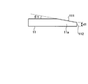
- FIG. 1 is a perspective view schematically showing a configuration of a conductive member according to the first exemplary embodiment of the present invention.
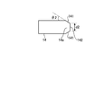
- FIG. 2 is a schematic diagram illustrating a configuration of a main part of the conductive member according to the first embodiment of the present invention.
- FIG. 3 is a schematic diagram showing an outline of a cold spray device used for manufacturing the conductive member according to the first embodiment of the present invention.
- FIG. 4 is a perspective view schematically showing the configuration of the conductive member according to the second embodiment of the present invention.
- FIG. 5 is a cross-sectional view schematically showing a configuration of a main part of the conductive member according to the second embodiment of the present invention.
- FIG. 6 is a schematic diagram illustrating a configuration of a main part of the conductive member according to the second embodiment of the present invention.
- FIG. 1 is a perspective view schematically showing a configuration of a conductive member according to the first embodiment.
- FIG. 2 is a schematic diagram illustrating a configuration of a main part of the conductive member according to the first embodiment.
- a conductive member 1 shown in FIG. 1 is arranged as a power supply line or the like, and is made of a substantially plate-like first conductive material 11 made of a light and inexpensive conductive material, and a conductive material having high electrical conductivity.
- a substantially plate-like second conductive material 12 and a metal film 13 formed between the first conductive material 11 and the second conductive material 12 are provided.
- the first conductive material 11 has a substantially plate shape, and has a tapered portion 11a in which one end portion has a tapered shape.
- the first conductive material 11 is formed of a light and inexpensive material such as aluminum or aluminum alloy.
- the second conductive material 12 has a substantially plate shape, and has a tapered portion 12a as a notched portion having a tapered shape on one end side.
- the second conductive material 12 is made of a material having high electrical conductivity, for example, copper, noble metal, copper alloy, or noble metal alloy having a lower electrical resistivity than aluminum.
- the tapered portion 11 a has an inclined surface 111 having a tapered shape in which one surface of the first conductive material 11 is cut out, and an end surface 112 in contact with the second conductive material 12.
- the inclination angle ⁇ 1 formed by the inclined surface 111 and the main surface of the first conductive material 11 is in the range of 0 ° to 45 °. More preferably, the inclination angle ⁇ 1 is in the range of 2 ° to 35 °.
- the tapered portion 11 a has a tapered shape so that the thickness d 1 of the end surface 112 is 0.1 to 0.5 times the maximum thickness of the first conductive material 11.
- the tapered portion 12a also has the same inclination angle and thickness as the above-described tapered portion 11a.
- the inclination angle and the thickness of an end surface are the same.
- the metal film 13 is formed on the surfaces of the tapered portion 11a of the first conductive material 11 and the tapered portion 12a of the second conductive material 12 by a cold spray method described later.
- the metal film 13 (film material) include metals such as copper, molybdenum, aluminum, tungsten, nickel, silver, and alloys containing at least one of these metals.
- the metal coating 13 can be applied to any metal or alloy having a density of 95% or more with respect to the bulk material and a thermal conductivity of 90% or more.
- the first conductive material 11 is preferably a combination of copper or copper alloy
- the second conductive material 12 is aluminum or aluminum alloy
- the metal film 13 is copper or copper alloy.
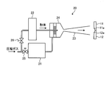
- FIG. 3 is a schematic diagram showing an outline of a cold spray apparatus used for forming the metal film 13. Formation of the metal film 13 by the cold spray method is performed by, for example, a cold spray device 20 shown in FIG.
- the cold spray device 20 contains a gas heater 21 that heats a compressed gas, a powder supply device 22 that contains a powder material to be sprayed on a sprayed material, and supplies the powder material to a spray gun 24, and a compressed gas heated by the spray gun 24. And a gas nozzle 23 that injects the mixed material powder toward the tapered portions 11a and 12a of the first conductive member 11 and the second conductive material 12.
- the compressed gas helium, nitrogen, air or the like is used.
- the supplied compressed gas is supplied to the gas heater 21 and the powder supply device 22 by valves 25 and 26, respectively.
- the compressed gas supplied to the gas heater 21 is heated to, for example, 50 to 700 ° C. and then supplied to the spray gun 24. More preferably, the compressed gas is heated so that the upper limit temperature of the powder injected onto the tapered portions 11a and 12a is kept below the melting point of the coating material. This is because the oxidation of the coating material can be suppressed by keeping the heating temperature of the powder material below the melting point of the coating material.
- the compressed gas supplied to the powder supply device 22 supplies, for example, material powder having a particle size of about 10 to 100 ⁇ m in the powder supply device 22 to the spray gun 24 so as to have a predetermined discharge amount.
- the heated compressed gas is converted into a supersonic flow (about 340 m / s or more) by a gas nozzle 23 having a tapered wide shape.
- the powder material supplied to the spray gun 24 is accelerated by the injection of this compressed gas into the supersonic flow, and forms a film by colliding with the formation surface of the tapered portions 11a and 12a at a high speed in the solid state. .
- the apparatus is not limited to the cold spray apparatus 20 of FIG. 3 as long as the apparatus can form a film by causing the material powder to collide with the taper portions 11a and 12a in a solid state.
- the surface of the taper portion 11a of the first conductive material 11 and the taper portion 12a of the second conductive material 12 can be covered with the metal film 13 by the above-described processing. If the surface of the first conductive material 11 and the second conductive material 12 is different from the surface on which the metal film 13 is formed after the coating is formed, surface processing such as cutting is performed as necessary to form the surface shape. May be adjusted.
- the metal film is formed and joined to the butt portion of the two conductive materials by the cold spray method.
- Conductive materials can be joined and have good electrical conductivity.
- the cold spray method can form a dense metal film with no phase transformation and suppressed oxidation as compared with welding or spraying methods that are processed at high temperatures.
- the metal properties of the film are superior to those of a metal film formed by thermal spraying or the like. Thereby, the electrical conductivity of a metal membrane
- the conductive member according to the first embodiment for a process of cutting a desired thickness after forming a base material by forming a metal film on a base material by a cold spray method, as in the past, There is no step of cutting, and the conductive member can be easily manufactured in a short time, and the yield can be improved and the manufacturing cost can be reduced.
- each conductive material is formed with a tapered part with a sloped surface, and this taper part is covered with a metal film, and the conductive materials are joined together. Compared with the case of joining materials, the contact area between the conductive materials through the metal film is increased, and thus the electrical resistance can be reduced. Thereby, high electrical conductivity can be realized.
- the taper portion has been described as having a cutout shape that forms a flat surface inclined with respect to the main surface of the conductive material.
- the taper-shaped forming surface may have an arcuate shape. Good.
- the inclined surface in a taper part was demonstrated as what is formed with respect to one surface of an electroconductive material, it may be formed in both surfaces, respectively.
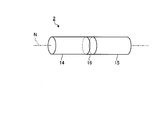
- FIG. 4 is a perspective view schematically showing the configuration of the conductive member according to the second embodiment.
- FIG. 5 is a cross-sectional view schematically showing a configuration of a main part of the conductive member according to the second embodiment.
- FIG. 5 is a cross-sectional view of the conductive member 2 shown in FIG. 4 cut along a plane including the central axis N in the longitudinal direction.
- FIG. 6 is a schematic diagram showing the first conductive material 14. The conductive member 2 shown in FIG.
- first conductive material 14 made of a light and inexpensive conductive material
- second conductive material made of a conductive material having high electrical conductivity.
- metal film 16 formed between the first conductive material 14 and the second conductive material 15.
- the first conductive material 14 has a substantially plate shape, and has a tapered portion 14a in which one end side has a tapered shape.
- the first conductive material 14 is formed of a light and inexpensive material such as aluminum or aluminum alloy.
- the second conductive material 15 has a substantially plate shape, and has a tapered portion 15a in which one end side has a tapered shape.
- the second conductive material 15 is formed of a material having high electrical conductivity, for example, copper, a noble metal, a copper alloy, or a noble metal alloy.
- the metal film 16 is formed on the surfaces of the tapered portion 14a of the first conductive material 14 and the tapered portion 15a of the second conductive material 15 by the cold spray device 20 of FIG.
- the metal film 16 include metals and alloys such as copper, molybdenum, aluminum, tungsten, nickel, and silver.
- the metal film 16 can be applied to any metal or alloy having a density of 95% or more with respect to the bulk material and a thermal conductivity of 90% or more.
- the tapered portion 14 a has an inclined surface 141 having a tapered shape in which the end portion of the first conductive material 14 is chamfered, and an end surface 142 in contact with the second conductive material 15.
- the inclination angle ⁇ 2 formed by the inclined surface 141 of the tapered portion 14a and the main surface of the first conductive material 14 is in the range of 0 ° to 45 ° as in the first embodiment. More preferably, the inclination angle ⁇ 2 is in the range of 2 ° to 35 °.
- the tapered portion 14a is formed in a tapered shape, the diameter d2 of the end surface 142 becomes 0.1 to 0.5 times the maximum diameter in the direction perpendicular to the central axis N of the first conductive material 14. It is preferable.
- the tapered portion 15a also has the same inclination angle and end face diameter as the tapered portion 14a described above.
- an inclination angle and the diameter of an end surface are the same.
- the metal film is formed and joined to the butt portion of the two conductive materials by the cold spray method. Regardless, it is possible to join a plurality of conductive materials at low cost and have good electrical conductivity.
- the cold spray method can form a dense metal film with no phase transformation and suppressed oxidation as compared with welding or spraying methods that are processed at high temperatures.
- the metal properties of the film are superior to those of a metal film formed by thermal spraying or the like. Thereby, the electrical conductivity of a metal membrane
- the conventional process of cutting out with a desired thickness after forming a base material by forming a metal film on a base material by a cold spray method is difficult to cut out in the cylindrical shape as in the second embodiment.
- the conductive member according to the second embodiment does not have a step of cutting, and the conductive member can be easily manufactured in a short time, and the yield can be improved and the manufacturing cost can be reduced.
- each conductive material is formed with a tapered part with a sloped surface, and this taper part is covered with a metal film, and the conductive materials are joined together. Compared with the case of joining materials, the contact area between the conductive materials through the metal film is increased, and thus the electrical resistance can be reduced. Thereby, high electrical conductivity can be realized.
- the conductive member according to the present invention is useful for producing a conductive member by joining a plurality of conductive materials.
Landscapes
- Chemical & Material Sciences (AREA)
- Chemical Kinetics & Catalysis (AREA)
- Engineering & Computer Science (AREA)
- Materials Engineering (AREA)
- Mechanical Engineering (AREA)
- Metallurgy (AREA)
- Organic Chemistry (AREA)
- Other Surface Treatments For Metallic Materials (AREA)
- Coating By Spraying Or Casting (AREA)
- Non-Insulated Conductors (AREA)
Abstract
Description
まず、本発明の実施の形態1にかかる導電部材について、図面を参照して詳細に説明する。図1は、本実施の形態1にかかる導電部材の構成を模式的に示す斜視図である。図2は、本実施の形態1にかかる導電部材の要部の構成を示す模式図である。図1に示す導電部材1は、電源供給ライン等として配設され、軽量で安価な導電性材料からなる略板状の第1導電性材料11と、高い電気伝導度を有する導電性材料からなる略板状の第2導電性材料12と、第1導電性材料11と第2導電性材料12との間に形成される金属皮膜13と、を備える。
つぎに、本発明の実施の形態2にかかる導電部材について、図面を参照して詳細に説明する。図4は、本実施の形態2にかかる導電部材の構成を模式的に示す斜視図である。図5は、本実施の形態2にかかる導電部材の要部の構成を模式的に示す断面図である。なお、図5は、図4に示す導電部材2を、長手方向の中心軸Nを含む平面で切断した断面図である。また、図6は、第1導電性材料14を示す模式図である。図4に示す導電部材2は、軽量で安価な導電性材料からなる略円柱状の第1導電性材料14と、高い電気伝導度を有する導電性材料からなる略円柱状の第2導電性材料15と、第1導電性材料14と第2導電性材料15との間に形成される金属皮膜16と、を備える。
11,14 第1導電性材料
11a,12a,14a,15a テーパ部
12,15 第2導電性材料
13,16 金属皮膜
20 コールドスプレー装置
21 ガス加熱器
22 粉末供給装置
23 ガスノズル
24 スプレーガン
25,26 バルブ
Claims (7)
- 少なくとも一方がアルミニウムよりも電気抵抗率の低い導電性材料からなる第1および第2導電性材料と、
前記第1および第2導電性材料が突き合わされた突合せ部分に対して、金属を含む粉体をガスと共に加速し、前記突合せ部分の表面に固相状態のままで吹き付けて堆積させることによって形成された金属皮膜と、
を備えたことを特徴とする導電部材。 - 前記第1および第2導電性材料は、突合せ側の端部に切り欠き形状をなす切欠部をそれぞれ有し、
前記金属皮膜は、前記切欠部を覆うことを特徴とする請求項1に記載の導電部材。 - 前記切欠部は、前記第1および第2導電性材料の各主面に対して傾斜したテーパ形状をなすことを特徴とする請求項2に記載の導電部材。
- 前記切欠部は、前記第1および第2導電性材料の各主面に対する傾斜角が、0°~45°であることを特徴とする請求項3に記載の導電部材。
- 前記切欠部は、前記第1および第2導電性材料の各主面に対する前記傾斜角が、2°~35°であることを特徴とする請求項4に記載の導電部材。
- 前記金属皮膜に用いる金属は、銅、モリブデン、アルミニウム、タングステン、ニッケル、銀またはこれらの少なくとも一つを含む合金からなる群より選択される少なくとも1種類を含むことを特徴とする請求項1~5のいずれか一つに記載の導電部材。
- 前記第1および第2導電性材料の他方は、アルミニウムまたはアルミニウム合金であることを特徴とする請求項1~6のいずれか一つに記載の導電部材。
Priority Applications (4)
| Application Number | Priority Date | Filing Date | Title |
|---|---|---|---|
| CN201180063714.1A CN103298975B (zh) | 2011-01-07 | 2011-12-26 | 导电构件 |
| US13/977,968 US9070487B2 (en) | 2011-01-07 | 2011-12-26 | Conductive member |
| EP11854649.8A EP2662473B1 (en) | 2011-01-07 | 2011-12-26 | Conductive member |
| KR1020137016179A KR101545222B1 (ko) | 2011-01-07 | 2011-12-26 | 도전 부재 |
Applications Claiming Priority (2)
| Application Number | Priority Date | Filing Date | Title |
|---|---|---|---|
| JP2011-002212 | 2011-01-07 | ||
| JP2011002212A JP5484360B2 (ja) | 2011-01-07 | 2011-01-07 | 導電部材 |
Publications (1)
| Publication Number | Publication Date |
|---|---|
| WO2012093614A1 true WO2012093614A1 (ja) | 2012-07-12 |
Family
ID=46457473
Family Applications (1)
| Application Number | Title | Priority Date | Filing Date |
|---|---|---|---|
| PCT/JP2011/080125 Ceased WO2012093614A1 (ja) | 2011-01-07 | 2011-12-26 | 導電部材 |
Country Status (6)
| Country | Link |
|---|---|
| US (1) | US9070487B2 (ja) |
| EP (1) | EP2662473B1 (ja) |
| JP (1) | JP5484360B2 (ja) |
| KR (1) | KR101545222B1 (ja) |
| CN (1) | CN103298975B (ja) |
| WO (1) | WO2012093614A1 (ja) |
Cited By (3)
| Publication number | Priority date | Publication date | Assignee | Title |
|---|---|---|---|---|
| WO2013021870A1 (ja) * | 2011-08-05 | 2013-02-14 | 日本発條株式会社 | 冷却装置及びその製造方法 |
| US20140339093A1 (en) * | 2013-05-20 | 2014-11-20 | Apple Inc. | Solid state deposition for cosmetic enhancement of anodized friction stir processed parts |
| US9951425B2 (en) | 2013-07-25 | 2018-04-24 | Apple Inc. | Solid state deposition methods, apparatuses, and products |
Families Citing this family (11)
| Publication number | Priority date | Publication date | Assignee | Title |
|---|---|---|---|---|
| JP5186528B2 (ja) * | 2010-04-23 | 2013-04-17 | 日本発條株式会社 | 導電部材及びその製造方法 |
| JP5712054B2 (ja) * | 2011-05-31 | 2015-05-07 | 日本発條株式会社 | シャフト付きヒータユニットおよびシャフト付きヒータユニットの製造方法 |
| JP2013072093A (ja) * | 2011-09-26 | 2013-04-22 | Toyota Motor Corp | 異種の金属部材の接続構造 |
| CN103247362B (zh) * | 2013-04-17 | 2016-02-03 | 隆科电子(惠阳)有限公司 | 一种电子陶瓷元件的卑金属复合电极及其制备方法 |
| JP6437365B2 (ja) * | 2015-03-30 | 2018-12-12 | タツタ電線株式会社 | 固定方法、被覆導線固定構造 |
| KR102422703B1 (ko) * | 2016-09-05 | 2022-07-19 | 렐리본드 에이피에스 | 전기적으로 도전성의 전력 전송 인터페이스를 제공하는 방법, 인터페이스 형성 장치 및 전력 전송 인터페이스를 형성하기 위한 냉간 스프레이 장치 |
| CN110328460B (zh) * | 2019-08-08 | 2021-09-21 | 广东省科学院新材料研究所 | 一种银不锈钢复合板的连接方法及其应用 |
| GB202004947D0 (en) * | 2020-04-03 | 2020-05-20 | Rolls Royce Plc | Joining component bodies |
| DE102020206009A1 (de) | 2020-05-13 | 2021-11-18 | Fraunhofer-Gesellschaft zur Förderung der angewandten Forschung eingetragener Verein | Verfahren zur Erzeugung einer stoffschlüssigen Verbindung im Verbundguss |
| CN117637243A (zh) * | 2022-08-09 | 2024-03-01 | 施耐德电气(中国)有限公司 | 母线装置 |
| KR102725834B1 (ko) * | 2024-07-09 | 2024-11-05 | 김낙경 | 구조 개선된 수배전반용 부스바 |
Citations (3)
| Publication number | Priority date | Publication date | Assignee | Title |
|---|---|---|---|---|
| JP2003522391A (ja) * | 2000-02-01 | 2003-07-22 | サウスウォール テクノロジーズ インコーポレイテッド | 透明導電膜上へのブスバーの真空堆積 |
| JP2009068032A (ja) * | 2007-09-11 | 2009-04-02 | Hitachi Ltd | 耐熱部材およびその製造方法 |
| JP2010016945A (ja) * | 2008-07-02 | 2010-01-21 | Showa Denko Kk | 水冷式ブスバー及びその製造方法 |
Family Cites Families (8)
| Publication number | Priority date | Publication date | Assignee | Title |
|---|---|---|---|---|
| DE69016433T2 (de) | 1990-05-19 | 1995-07-20 | Papyrin Anatolij Nikiforovic | Beschichtungsverfahren und -vorrichtung. |
| JPH0593254A (ja) * | 1991-09-30 | 1993-04-16 | Sumitomo Metal Ind Ltd | 金属接合方法 |
| JPH11154435A (ja) * | 1997-11-19 | 1999-06-08 | Toshiba Corp | 異種金属材料の接合構造 |
| DE19747383A1 (de) * | 1997-10-27 | 1999-04-29 | Linde Ag | Verbinden von Werkstücken |
| JP4433650B2 (ja) * | 2001-10-03 | 2010-03-17 | 日本碍子株式会社 | リチウム二次単電池及びリチウム二次単電池の接続構造体 |
| KR20080010086A (ko) * | 2006-07-26 | 2008-01-30 | (주)태광테크 | 저온분사 코팅법을 이용한 부스바 제조방법 |
| JP2010142101A (ja) * | 2008-12-15 | 2010-06-24 | Tousui Ltd | ブスバー |
| US20100170937A1 (en) * | 2009-01-07 | 2010-07-08 | General Electric Company | System and Method of Joining Metallic Parts Using Cold Spray Technique |
-
2011
- 2011-01-07 JP JP2011002212A patent/JP5484360B2/ja active Active
- 2011-12-26 KR KR1020137016179A patent/KR101545222B1/ko active Active
- 2011-12-26 US US13/977,968 patent/US9070487B2/en active Active
- 2011-12-26 CN CN201180063714.1A patent/CN103298975B/zh active Active
- 2011-12-26 EP EP11854649.8A patent/EP2662473B1/en active Active
- 2011-12-26 WO PCT/JP2011/080125 patent/WO2012093614A1/ja not_active Ceased
Patent Citations (3)
| Publication number | Priority date | Publication date | Assignee | Title |
|---|---|---|---|---|
| JP2003522391A (ja) * | 2000-02-01 | 2003-07-22 | サウスウォール テクノロジーズ インコーポレイテッド | 透明導電膜上へのブスバーの真空堆積 |
| JP2009068032A (ja) * | 2007-09-11 | 2009-04-02 | Hitachi Ltd | 耐熱部材およびその製造方法 |
| JP2010016945A (ja) * | 2008-07-02 | 2010-01-21 | Showa Denko Kk | 水冷式ブスバー及びその製造方法 |
Non-Patent Citations (1)
| Title |
|---|
| See also references of EP2662473A4 * |
Cited By (4)
| Publication number | Priority date | Publication date | Assignee | Title |
|---|---|---|---|---|
| WO2013021870A1 (ja) * | 2011-08-05 | 2013-02-14 | 日本発條株式会社 | 冷却装置及びその製造方法 |
| US20140339093A1 (en) * | 2013-05-20 | 2014-11-20 | Apple Inc. | Solid state deposition for cosmetic enhancement of anodized friction stir processed parts |
| US9611562B2 (en) * | 2013-05-20 | 2017-04-04 | Apple Inc. | Solid state deposition for cosmetic enhancement of anodized friction stir processed parts |
| US9951425B2 (en) | 2013-07-25 | 2018-04-24 | Apple Inc. | Solid state deposition methods, apparatuses, and products |
Also Published As
| Publication number | Publication date |
|---|---|
| JP2012144759A (ja) | 2012-08-02 |
| KR101545222B1 (ko) | 2015-08-18 |
| EP2662473A1 (en) | 2013-11-13 |
| US9070487B2 (en) | 2015-06-30 |
| JP5484360B2 (ja) | 2014-05-07 |
| KR20130087587A (ko) | 2013-08-06 |
| US20130292152A1 (en) | 2013-11-07 |
| CN103298975B (zh) | 2015-04-29 |
| CN103298975A (zh) | 2013-09-11 |
| EP2662473B1 (en) | 2019-01-23 |
| EP2662473A4 (en) | 2016-05-11 |
Similar Documents
| Publication | Publication Date | Title |
|---|---|---|
| JP5484360B2 (ja) | 導電部材 | |
| KR101502038B1 (ko) | 도전 부재 및 그 제조 방법 | |
| JP5654089B1 (ja) | 積層体および積層体の製造方法 | |
| JP2012201890A (ja) | 積層体、導電材料および積層体の製造方法 | |
| JP2008115467A (ja) | 構成部品の接合面に充填材を堆積させる方法 | |
| WO2012165440A1 (ja) | シャフト付きヒータユニットおよびシャフト付きヒータユニットの製造方法 | |
| CN111869061B (zh) | 用于制造鼠笼式转子的方法 | |
| TWI641441B (zh) | 焊錫連接構造及成膜方法 | |
| WO2015005130A1 (ja) | 導電部材および導電部材の製造方法 | |
| JP2012153581A (ja) | セラミックスとアルミニウムとの接合方法 | |
| JP2013245375A (ja) | ツバ付きターゲットの製造方法 | |
| US7900812B2 (en) | Secure physical connections formed by a kinetic spray process | |
| JP2012144758A (ja) | 導電用端子 | |
| JP2017036464A (ja) | 導電部材、ガス絶縁開閉装置用導電部材およびガス絶縁開閉装置用導電部材の製造方法 | |
| CN105144333A (zh) | 用于制造真空开关管的构件的方法 | |
| JP5889938B2 (ja) | 積層体および積層体の製造方法 | |
| JP3888077B2 (ja) | 金属接合用電極及びその製造方法、並びに金属接合用電極を備えた溶接設備及びそれにより溶接された製品 | |
| TWI381900B (zh) | Metal bonding structure and joining method thereof | |
| EP3703187B1 (en) | Electric wire joining structure, electric wire joining method, and terminal | |
| JP4997485B2 (ja) | 導電性を有する微小球体の接合体及び接合方法 | |
| KR20100075244A (ko) | 이종 도체 슬리브 제조방법 |
Legal Events
| Date | Code | Title | Description |
|---|---|---|---|
| 121 | Ep: the epo has been informed by wipo that ep was designated in this application |
Ref document number: 11854649 Country of ref document: EP Kind code of ref document: A1 |
|
| ENP | Entry into the national phase |
Ref document number: 20137016179 Country of ref document: KR Kind code of ref document: A |
|
| WWE | Wipo information: entry into national phase |
Ref document number: 13977968 Country of ref document: US Ref document number: 2011854649 Country of ref document: EP |
|
| NENP | Non-entry into the national phase |
Ref country code: DE |