WO2012098741A1 - 制御システム - Google Patents
制御システム Download PDFInfo
- Publication number
- WO2012098741A1 WO2012098741A1 PCT/JP2011/074043 JP2011074043W WO2012098741A1 WO 2012098741 A1 WO2012098741 A1 WO 2012098741A1 JP 2011074043 W JP2011074043 W JP 2011074043W WO 2012098741 A1 WO2012098741 A1 WO 2012098741A1
- Authority
- WO
- WIPO (PCT)
- Prior art keywords
- frequency
- clock
- function
- unit
- voltage
- Prior art date
- Legal status (The legal status is an assumption and is not a legal conclusion. Google has not performed a legal analysis and makes no representation as to the accuracy of the status listed.)
- Ceased
Links
Images






Classifications
-
- G—PHYSICS
- G06—COMPUTING OR CALCULATING; COUNTING
- G06F—ELECTRIC DIGITAL DATA PROCESSING
- G06F1/00—Details not covered by groups G06F3/00 - G06F13/00 and G06F21/00
- G06F1/04—Generating or distributing clock signals or signals derived directly therefrom
-
- G—PHYSICS
- G06—COMPUTING OR CALCULATING; COUNTING
- G06F—ELECTRIC DIGITAL DATA PROCESSING
- G06F1/00—Details not covered by groups G06F3/00 - G06F13/00 and G06F21/00
- G06F1/26—Power supply means, e.g. regulation thereof
- G06F1/32—Means for saving power
- G06F1/3203—Power management, i.e. event-based initiation of a power-saving mode
- G06F1/3234—Power saving characterised by the action undertaken
- G06F1/324—Power saving characterised by the action undertaken by lowering clock frequency
-
- G—PHYSICS
- G06—COMPUTING OR CALCULATING; COUNTING
- G06F—ELECTRIC DIGITAL DATA PROCESSING
- G06F1/00—Details not covered by groups G06F3/00 - G06F13/00 and G06F21/00
- G06F1/26—Power supply means, e.g. regulation thereof
- G06F1/32—Means for saving power
- G06F1/3203—Power management, i.e. event-based initiation of a power-saving mode
- G06F1/3234—Power saving characterised by the action undertaken
- G06F1/3296—Power saving characterised by the action undertaken by lowering the supply or operating voltage
-
- Y—GENERAL TAGGING OF NEW TECHNOLOGICAL DEVELOPMENTS; GENERAL TAGGING OF CROSS-SECTIONAL TECHNOLOGIES SPANNING OVER SEVERAL SECTIONS OF THE IPC; TECHNICAL SUBJECTS COVERED BY FORMER USPC CROSS-REFERENCE ART COLLECTIONS [XRACs] AND DIGESTS
- Y02—TECHNOLOGIES OR APPLICATIONS FOR MITIGATION OR ADAPTATION AGAINST CLIMATE CHANGE
- Y02D—CLIMATE CHANGE MITIGATION TECHNOLOGIES IN INFORMATION AND COMMUNICATION TECHNOLOGIES [ICT], I.E. INFORMATION AND COMMUNICATION TECHNOLOGIES AIMING AT THE REDUCTION OF THEIR OWN ENERGY USE
- Y02D10/00—Energy efficient computing, e.g. low power processors, power management or thermal management
Definitions
- the present invention relates to a control system and a control device that control a power supply voltage and a clock frequency to be supplied.
- DVFS Dynamic Voltage and Frequency Scaling
- This function realizes power saving by appropriately setting the required frequency and the appropriate voltage in the system.
- the CPU Central Processing Unit
- IEM for example, see Non-Patent Document 1.
- a method is used in which a voltage and a frequency when a specific application is started are defined in advance without using a function such as IEM, and the voltage and frequency defined by software judgment are set by software. .
- FIG. 1 is a time chart showing an example of timing when the frequency of a clock supplied to the CPU is switched from low to high by a general DVFS.
- FIG. 2 is a time chart showing an example of timing when the frequency of the clock supplied to the CPU is switched from high to low by general DVFS.
- the frequency cannot be increased when the necessary voltage is not applied. Whether it is necessary to increase or decrease the frequency is managed by software, but the management of software becomes complicated and the processing of the system increases for management. There is.
- An object of the present invention is to provide a control system and a control device that solve the above-described problems.
- the control system of the present invention In a control system composed of a power supply device capable of supplying power of a plurality of voltages and a control device connected to the power supply device and a CPU,
- the controller is A storage unit for storing a voltage and a clock frequency required for each of a plurality of functions of the CPU;
- a power control unit that instructs the power supply device to supply the power at the highest voltage among the voltages corresponding to the function that is operating among the plurality of functions stored in the storage unit.
- a clock supply unit configured to supply a clock having the highest frequency to the CPU among the frequencies corresponding to the function being operated among the plurality of functions stored in the storage unit;
- the power supply device A power supply unit for supplying the power to the CPU at a voltage instructed by the power control unit;
- an interrupt notification unit that notifies the control device when the change is completed,
- the power supply control unit changes the frequency to the frequency according to the function.
- the clock supply unit responds to the function after receiving the notification from the interrupt notification unit. A clock having a frequency is supplied.
- control device of the present invention A control device, A storage unit that stores a voltage and a clock frequency required for each of a plurality of functions of a CPU connected to the control device; A power supply device that supplies power to the CPU so as to supply power at the highest voltage among the voltages corresponding to the function of the plurality of functions that is stored in the storage unit.
- a power control unit for instructing A clock supply unit configured to supply a clock having the highest frequency to the CPU among the frequencies corresponding to the function being operated among the plurality of functions stored in the storage unit; When switching to a function in which the frequency of the clock supplied by the clock supply unit is lower than the frequency currently supplied by the clock supply unit occurs, the power supply control unit changes the frequency to the frequency according to the function.
- the clock supply unit Instructing the power supply to be supplied at a voltage corresponding to the frequency after the switching is completed, When switching to a function in which the frequency of the clock to be supplied is higher than the currently supplied frequency occurs, the clock supply unit completes the change of the voltage supplied from the power supply device, and then A clock with a frequency according to the function is supplied.
- FIG. 4 is a flowchart for explaining processing using a flag table when an operating function is switched among a plurality of functions included in the CPU shown in FIG. 3 in the present embodiment. It is a flowchart for demonstrating a process when there exists a change in the flag of the flag table memorize
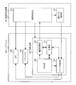
- FIG. 3 is a diagram showing an embodiment of the control system of the present invention.
- this embodiment includes a system LSI 100 and a power supply device 500 that is a power supply LSI that supplies power to the system LSI 100.
- the system LSI 100 is provided with a control device 200, which is a power frequency control unit, a CPU 300, and a peripheral 400.
- the power supply device 500 is provided with a power supply unit 510 and an interrupt notification unit 520.
- control device 200 is provided with a storage unit 210, a power supply control unit 220, a clock supply unit 230, and a determination unit 240.
- the storage unit 210 stores in advance the voltage and clock frequency required for each of the plurality of functions of the CPU 300. Note that the storage unit 210 may be configured by a register.
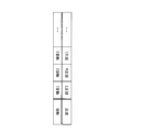
- FIG. 4 is a diagram illustrating an example of correspondence between functions and settings stored in the storage unit 210 illustrated in FIG.
- the storage unit 210 shown in FIG. 3 stores a plurality of functions provided in the CPU 300 in association with settings necessary for the functions to operate.
- the “function” stored here may be information for identifying an operating function.
- the “setting” stored here may be information that can specify the setting for operation.
- FIG. 5 is a diagram showing an example of setting contents such as voltage and frequency stored in the storage unit 210 shown in FIG.
- the storage unit 210 shown in FIG. 3 stores a voltage (voltage value) and a frequency in association with each of the plurality of settings shown in FIG.
- n settings from setting 1 to setting n n is a natural number
- n sets of setting contents are stored. This setting content is set in advance from the outside.
- the communication interface between the CPU 300 and the power supply device 500 is IIC
- settings such as a power supply voltage and a clock frequency necessary for the communication function are stored.
- an address or a sub address where a voltage value is set may be set.
- setting 1 (low order) has the lowest voltage and frequency
- setting n (high order) has the highest voltage and frequency. That is, the voltage and frequency increase in order from setting 1 to setting n.
- the storage unit 210 stores counter values corresponding to a plurality of settings as a counter table.
- FIG. 6 is a diagram illustrating an example of a counter table stored in the storage unit 210 illustrated in FIG.
- the storage unit 210 shown in FIG. 3 stores counter values corresponding to the plurality of settings shown in FIG.
- the stored counter value is a value counted by a counter (not shown) provided in the control device 200.
- the counter value of the setting m is incremented in the counter table. Also, if the setting m is no longer necessary, that is, if the operation of the function that requires the setting m is stopped, the counter value of the setting m in the counter table is decremented.
- the reason for using the counter is that the setting of each DVFS is not assigned to each function, but for example, there may be two or more functions that require setting m. This is because if the counter value is 0, the frequency m of the setting m is unnecessary, and if it is 1 or more, it is determined that it is necessary.
- the upper limit of the counter is 255 (a function that can be registered for one setting), the counter may be 1 byte for each setting.
- setting 1 is the lowest and setting n is the highest in FIG.
- the determination unit 240 determines that a function switching has occurred when a function that is not operating is activated or a function that is operating is stopped among a plurality of functions included in the CPU 300. Further, when the determination unit 240 determines that the function switching has occurred, the determination unit 240 compares the frequency of the clock supplied by the clock supply unit 230 with the frequency currently supplied by the clock supply unit 230.
- the power supply control unit 220 instructs the power supply device 500 to supply power at the highest voltage among the voltages corresponding to the function that is operating stored in the storage unit 210. To do. In addition, when switching to a function in which the frequency of the clock supplied by the clock supply unit 230 is lower than the frequency currently supplied by the clock supply unit 230 occurs, the power supply control unit 220 has a frequency corresponding to the function. After the switching to is completed, the power supply device 500 is instructed to supply power at a voltage corresponding to the frequency after the switching.
- the power supply control unit 220 performs the above-described processing based on the comparison result in the determination unit 240.
- the clock supply unit 230 generates a clock having the highest frequency among the frequencies stored in the storage unit 210 according to the function that is operating, and supplies the clock to the CPU 300. In addition, when switching to a function in which the frequency of the clock to be supplied is higher than the currently supplied frequency occurs, the clock supply unit 230 receives a notification from the interrupt notification unit 520 and then responds to the function. Supply a clock with a different frequency.
- the clock supply unit 230 compares the frequency of the clock to be supplied with the currently supplied frequency, and described above based on the comparison result. Process.
- CPU 300 controls control device 200 and peripheral 400. Further, the CPU 300 has a plurality of functions.
- the peripheral 400 is a general peripheral function excluding the memory in the system LSI 100 and includes a plurality of functions (devices). In the present embodiment, the peripheral 400 is collectively referred to as the peripheral 400.
- the power supply unit 510 can supply power of a plurality of voltages.
- the power supply unit 510 supplies power (CPU power) to the CPU 300 at a voltage instructed by the power control unit 220.
- the power supply unit 510 supplies power (peripheral power) to the peripheral 400 at a voltage instructed by the power control unit 220.
- the power supply unit 510 supplies power of a predetermined voltage (control device power) to the control device 200.
- the interrupt notification unit 520 When the voltage of the power supplied from the power supply unit 510 is changed, the interrupt notification unit 520 notifies the clock supply unit 230 of the control device 200 with an interrupt signal when the change is completed.
- the interface between the system LSI 100 and the power supply device 500 may be an interface such as a serial bus, and is not particularly defined here.
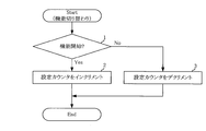
- FIG. 7 is a flowchart for explaining processing in the present embodiment when an operating function is switched among a plurality of functions included in the CPU 300 shown in FIG. 3.
- step 1 when the function is switched, it is determined by the determination unit 240 in step 1 whether the function that has not been operated is started or whether the function that has been operated is terminated.
- the setting required by the function is read from the storage unit 210, and in step 2, a counter corresponding to the read setting is incremented.
- the incremented counter value is stored in association with the corresponding setting in the counter table in the storage unit 210.
- the setting required by the function is read from the storage unit 210, and in step 3, the counter corresponding to the read setting is decremented. .
- the decremented counter value is stored in association with the corresponding setting in the counter table in the storage unit 210.
- This process is a hardware process when the processes of Step 2 and Step 3 described with reference to FIG. 7 are performed.
- FIG. 8 is a flowchart for explaining processing when there is a change in the counter value of the counter table stored in the storage unit 210 shown in FIG.
- a case where the setting in which the counter value has changed on the counter table is “setting m” will be described as an example.
- the determination unit 240 determines in step 12 whether or not the change in the counter value is from “1” to “0”.
- Step 13 If the change in the counter value is not a change from “1” to “0”, whether or not the change in the counter value is from “0” to “1” is determined in Step 13 by the determination unit 240. Is determined by
- the change in the counter value is a change from “0” to “1”
- the frequency of the clock is increased. Therefore, the voltage associated with the setting m is stored in the storage unit 210 by the power supply control unit 220.
- the power supply control unit 220 instructs the power supply unit 510 to supply power with the read voltage.
- the power supply unit 510 changes the voltage of the power to be supplied.
- FIG. 9 is a flowchart for explaining processing in the power supply apparatus 500 instructed to supply power by the processing in step 14 in FIG.
- the power supply unit 510 When the power supply unit 510 is instructed to supply power by specifying a voltage from the power supply control unit 220, the voltage of the power supply to be supplied is changed in step 31.
- the power supply unit 510 When the voltage change is completed, the power supply unit 510 notifies the interrupt notification unit 520 to that effect, and in step 32, the voltage change completion notification is output from the interrupt notification unit 520 to the clock supply unit 230 of the control device 200.
- the This notification may be output as an interrupt signal.
- FIG. 10 is a diagram illustrating an example of the timing of the voltage change completion notification (interrupt notification) output from the power supply apparatus 500 illustrated in FIG.
- FIG. 11 is a diagram illustrating another example of the timing of the voltage change completion notification (interrupt notification) output from the power supply apparatus 500 illustrated in FIG.
- an interrupt notification is output.
- the case where the interrupt notification is a positive pulse signal (the pulse width is arbitrary) is shown as an example, but a negative pulse signal is used. Some may be determined by a rising edge or a falling edge using a level signal.
- the power having the changed voltage value is supplied from the power supply unit 510 to the CPU 300.
- step 14 the process is not performed until the voltage change is completed in step 15. Specifically, the process is in a wait state until a voltage change completion notification is output from the power supply apparatus 500.
- the clock supply unit 230 reads the frequency associated with the setting m from the storage unit 210 and supplies it to the CPU 300 in step 16. Set (generated) as the clock frequency. In step 17, the process waits until the setting is completed, that is, until the frequency change is completed.
- a clock having a set frequency is supplied from the clock supply unit 230 to the CPU 300.
- step 12 if the change in the counter value is a change from “1” to “0” in step 12, it indicates that all functions that require setting m are not used. Therefore, setting m is not necessary.
- the setting next to the setting m is searched for among the settings whose counter value is 1 or more on the counter table.
- setting 3 is searched will be described as an example.
- the frequency and voltage of setting m are reduced to the frequency and voltage of setting 3.
- the processing is performed to lower the voltage after lowering the frequency.
- the frequency corresponding to the setting 3 is read from the storage unit 210 by the clock supply unit 230 and set (generated) as the frequency of the clock supplied to the CPU 300 in step 18.
- the process waits until the setting is completed, that is, the frequency change is completed.
- a clock having a set frequency is supplied from the clock supply unit 230 to the CPU 300.
- step 20 the power supply control unit 220 instructs the power supply unit 510 to supply power with the read voltage.
- step 21 the process is not performed until the voltage change is completed. Specifically, the process is in a wait state until a voltage change completion notification is output from the power supply apparatus 500. Then, the process ends.
- a flag indicating whether the function (setting) is operating may be used instead of the counter table described above.
- FIG. 12 is a diagram showing an example of a flag table stored in the storage unit 210 shown in FIG.
- flags from FL1 to FLn are stored in each setting from setting 1 to setting n.
- the setting flag that is operating may be “On”, and the setting flag that is not operating may be “Off”.
- “On” may be “1” and “Off” may be “0”.
- FIG. 13 is a flowchart for explaining processing using a flag table in the present embodiment when the operating function is switched among the plurality of functions of the CPU 300 shown in FIG.
- the determination unit 240 determines in step 41 whether the function that has not been operated is started or whether the function that has been operated is terminated.
- step 42 the setting required by the function is read from the storage unit 210, and the flag corresponding to the read setting is set to “On”. Set (rewritten).
- the setting required by the function is read from the storage unit 210, and the flag corresponding to the read setting is “Off” in step 43. Set to (rewritten).
- FIG. 14 is a flowchart for explaining a process when there is a change in the flag of the flag table stored in the storage unit 210 shown in FIG.
- a case where the setting in which the flag has changed on the flag table is “setting m” will be described as an example.
- step 51 the determination unit 240 determines.
- the determination unit 240 determines in step 52 whether the setting m is “On” among the settings where the setting m is “On”. The For example, if the highest setting of which the flag was “On” before this processing is setting 3, the setting m becomes the highest by this processing.
- the power control unit 220 instructs the power supply unit 510 to supply power with the read voltage.
- the power supply unit 510 changes the voltage of the power to be supplied, and the power having the changed voltage value is supplied from the power supply unit 510 to the CPU 300.
- step 53 the process is not performed until the voltage change is completed in step 54. Specifically, the process is in a wait state until a voltage change completion notification is output from the power supply apparatus 500. This voltage change completion notification is the same as described above.
- the clock supply unit 230 reads the frequency associated with the setting m from the storage unit 210 and supplies it to the CPU 300 in step 55. Set (generated) as the clock frequency. In step 56, the process waits until the setting is completed, that is, the frequency change is completed.
- a clock having a set frequency is supplied from the clock supply unit 230 to the CPU 300.
- step 51 determines whether or not the change is from “On” to “Off”, whether or not the setting m is the highest setting among the settings that are “On” in step 57. Is determined by the determination unit 240.
- the frequency and voltage of setting m are reduced to the frequency and voltage of setting 3.
- the processing is performed to lower the voltage after lowering the frequency.
- the frequency corresponding to the setting 3 is read from the storage unit 210 by the clock supply unit 230 and set (generated) as the frequency of the clock supplied to the CPU 300 in step 58.
- the process waits until the setting is completed, that is, the frequency change is completed.
- a clock having a set frequency is supplied from the clock supply unit 230 to the CPU 300.
- step 60 the power supply control unit 220 instructs the power supply unit 510 to supply power at the read voltage.
- step 61 processing is not performed until the voltage change is completed. Specifically, the process is in a wait state until a voltage change completion notification is output from the power supply apparatus 500. Then, the process ends.
- the frequency and power supply voltage of the clock supplied to the peripheral 400 may be controlled.
- the software may simply perform a process of notifying the system LSI 100. Therefore, it is possible to satisfy power saving while simplifying software development.
- the fields of use of the present invention include mobile devices such as mobile terminals such as mobile phones and smartphones, mobile game machines, and mobile PCs.
Landscapes
- Engineering & Computer Science (AREA)
- Theoretical Computer Science (AREA)
- Physics & Mathematics (AREA)
- General Engineering & Computer Science (AREA)
- General Physics & Mathematics (AREA)
- Power Sources (AREA)
Abstract
Description
複数の電圧の電源を供給可能な電源供給装置と、該電源供給装置およびCPUと接続された制御装置とから構成された制御システムにおいて、
前記制御装置は、
前記CPUが具備する複数の機能それぞれに必要な電圧およびクロックの周波数を記憶する記憶部と、
前記記憶部に記憶されている、前記複数の機能のうちの動作している機能に応じた電圧の中で、最も高い電圧で前記電源を供給するように前記電源供給装置へ指示する電源制御部と、
前記記憶部に記憶されている、前記複数の機能のうちの動作している機能に応じた周波数の中で、最も高い周波数のクロックを前記CPUへ供給するクロック供給部とを有し、
前記電源供給装置は、
前記電源制御部から指示された電圧で前記電源を前記CPUへ供給する電源供給部と、
前記電源供給部から供給する電源の電圧が変更された場合、該変更が完了した際、前記制御装置へその旨を通知する割り込み通知部とを有し、
前記電源制御部は、前記クロック供給部が供給するクロックの周波数が、前記クロック供給部が現在供給している周波数よりも低くなる機能への切り替えが発生した場合、該機能に応じた周波数への切り替えが完了してから、該切り替え後の周波数に応じた電圧で前記電源を供給するように指示し、
前記クロック供給部は、供給するクロックの周波数が、現在供給している周波数よりも高くなる機能への切り替えが発生した場合、前記割り込み通知部からの前記通知を受けてから、該機能に応じた周波数のクロックを供給することを特徴とする。
制御装置であって、
当該制御装置と接続されたCPUが具備する複数の機能それぞれに必要な電圧およびクロックの周波数を記憶する記憶部と、
前記記憶部に記憶されている、前記複数の機能のうちの動作している機能に応じた電圧の中で、最も高い電圧で電源を供給するように、前記CPUへ電源を供給する電源供給装置へ指示する電源制御部と、
前記記憶部に記憶されている、前記複数の機能のうちの動作している機能に応じた周波数の中で、最も高い周波数のクロックを前記CPUへ供給するクロック供給部とを有し、
前記電源制御部は、前記クロック供給部が供給するクロックの周波数が、前記クロック供給部が現在供給している周波数よりも低くなる機能への切り替えが発生した場合、該機能に応じた周波数への切り替えが完了してから、該切り替え後の周波数に応じた電圧で前記電源を供給するように指示し、
前記クロック供給部は、供給するクロックの周波数が、現在供給している周波数よりも高くなる機能への切り替えが発生した場合、前記電源供給装置から供給される電圧の変更が完了してから、該機能に応じた周波数のクロックを供給する。
Claims (5)
- 複数の電圧の電源を供給可能な電源供給装置と、該電源供給装置およびCPUと接続された制御装置とから構成された制御システムにおいて、
前記制御装置は、
前記CPUが具備する複数の機能それぞれに必要な電圧およびクロックの周波数を記憶する記憶部と、
前記記憶部に記憶されている、前記複数の機能のうちの動作している機能に応じた電圧の中で、最も高い電圧で前記電源を供給するように前記電源供給装置へ指示する電源制御部と、
前記記憶部に記憶されている、前記複数の機能のうちの動作している機能に応じた周波数の中で、最も高い周波数のクロックを前記CPUへ供給するクロック供給部とを有し、
前記電源供給装置は、
前記電源制御部から指示された電圧で前記電源を前記CPUへ供給する電源供給部と、
前記電源供給部から供給する電源の電圧が変更された場合、該変更が完了した際、前記制御装置へその旨を通知する割り込み通知部とを有し、
前記電源制御部は、前記クロック供給部が供給するクロックの周波数が、前記クロック供給部が現在供給している周波数よりも低くなる機能への切り替えが発生した場合、該機能に応じた周波数への切り替えが完了してから、該切り替え後の周波数に応じた電圧で前記電源を供給するように指示し、
前記クロック供給部は、供給するクロックの周波数が、現在供給している周波数よりも高くなる機能への切り替えが発生した場合、前記割り込み通知部からの前記通知を受けてから、該機能に応じた周波数のクロックを供給することを特徴とする制御システム。 - 請求項1に記載の制御システムにおいて、
前記複数の機能のうち、動作していない機能が起動した際、または動作している機能が停止した際、機能の切り替えが発生したと判定し、前記機能の切り替えが発生したと判定した際、前記クロック供給部が供給するクロックの周波数と、前記クロック供給部が現在供給している周波数とを比較する判定部を有し、
前記電源制御部は、前記判定部における比較に結果に基づいて、前記指示を行い、
前記クロック供給部は、前記判定部における比較に結果に基づいて、前記クロックを供給することを特徴とする制御システム。 - 請求項2に記載の制御システムにおいて、
前記記憶部は、前記複数の機能それぞれが動作しているかどうかを示すフラグを記憶し、前記判定部が機能の切り替えが発生したと判定した際、該切り替えに基づいて前記フラグを書き換えることを特徴とする制御システム。 - 請求項1に記載の制御システムにおいて、
前記記憶部は、当該制御装置と接続された複数の装置それぞれに必要な電圧およびクロックの周波数を記憶し、
前記電源制御部は、前記記憶部に記憶されている、前記複数の装置のうちの動作している装置に応じた電圧の中で、最も高い電圧で前記電源を供給するように前記電源供給装置へ指示し、
前記クロック供給部は、前記記憶部に記憶されている、前記複数の装置のうちの動作している装置に応じた周波数の中で、最も高い周波数のクロックを該装置へ供給し、
前記電源供給部は、前記電源制御部から指示された電圧で前記電源を該装置へ供給することを特徴とする制御システム。 - 制御装置であって、
当該制御装置と接続されたCPUが具備する複数の機能それぞれに必要な電圧およびクロックの周波数を記憶する記憶部と、
前記記憶部に記憶されている、前記複数の機能のうちの動作している機能に応じた電圧の中で、最も高い電圧で電源を供給するように、前記CPUへ電源を供給する電源供給装置へ指示する電源制御部と、
前記記憶部に記憶されている、前記複数の機能のうちの動作している機能に応じた周波数の中で、最も高い周波数のクロックを前記CPUへ供給するクロック供給部とを有し、
前記電源制御部は、前記クロック供給部が供給するクロックの周波数が、前記クロック供給部が現在供給している周波数よりも低くなる機能への切り替えが発生した場合、該機能に応じた周波数への切り替えが完了してから、該切り替え後の周波数に応じた電圧で前記電源を供給するように指示し、
前記クロック供給部は、供給するクロックの周波数が、現在供給している周波数よりも高くなる機能への切り替えが発生した場合、前記電源供給装置から供給される電圧の変更が完了してから、該機能に応じた周波数のクロックを供給する制御装置。
Priority Applications (4)
| Application Number | Priority Date | Filing Date | Title |
|---|---|---|---|
| CN201180065494.6A CN103329064B (zh) | 2011-01-20 | 2011-10-19 | 控制系统 |
| EP11856057.2A EP2667284A4 (en) | 2011-01-20 | 2011-10-19 | CONTROL SYSTEM |
| US13/977,415 US20130297953A1 (en) | 2011-01-20 | 2011-10-19 | Control system |
| JP2012553560A JP5870935B2 (ja) | 2011-01-20 | 2011-10-19 | 制御システム |
Applications Claiming Priority (2)
| Application Number | Priority Date | Filing Date | Title |
|---|---|---|---|
| JP2011009722 | 2011-01-20 | ||
| JP2011-009722 | 2011-01-20 |
Publications (1)
| Publication Number | Publication Date |
|---|---|
| WO2012098741A1 true WO2012098741A1 (ja) | 2012-07-26 |
Family
ID=46515383
Family Applications (1)
| Application Number | Title | Priority Date | Filing Date |
|---|---|---|---|
| PCT/JP2011/074043 Ceased WO2012098741A1 (ja) | 2011-01-20 | 2011-10-19 | 制御システム |
Country Status (5)
| Country | Link |
|---|---|
| US (1) | US20130297953A1 (ja) |
| EP (1) | EP2667284A4 (ja) |
| JP (1) | JP5870935B2 (ja) |
| CN (1) | CN103329064B (ja) |
| WO (1) | WO2012098741A1 (ja) |
Cited By (2)
| Publication number | Priority date | Publication date | Assignee | Title |
|---|---|---|---|---|
| JP2014137823A (ja) * | 2013-01-17 | 2014-07-28 | Samsung Electronics Co Ltd | バッテリ及び電源供給装置並びに電子装置 |
| JP2016181168A (ja) * | 2015-03-24 | 2016-10-13 | シャープ株式会社 | 情報処理装置、cpu印加電圧制御装置、情報処理装置の制御方法 |
Families Citing this family (5)
| Publication number | Priority date | Publication date | Assignee | Title |
|---|---|---|---|---|
| DE102015112253A1 (de) | 2014-08-26 | 2016-03-03 | Samsung Electronics Co., Ltd. | Integrierte Leistungsverwaltungsschaltung, Leistungsverwaltungsverfahren, mobile Vorrichtung und Takteinstellverfahren |
| KR102320399B1 (ko) | 2014-08-26 | 2021-11-03 | 삼성전자주식회사 | 전원 관리 칩, 그것을 포함하는 모바일 장치 및 그것의 클록 조절 방법 |
| US20160055615A1 (en) * | 2014-11-11 | 2016-02-25 | Mediatek Inc. | Smart Frequency Boost For Graphics-Processing Hardware |
| JP6418971B2 (ja) * | 2015-02-05 | 2018-11-07 | キヤノン株式会社 | 情報処理装置及びその制御方法 |
| CN110134217B (zh) * | 2019-04-10 | 2021-03-23 | 深圳市普威技术有限公司 | 一种cpu功耗管理装置 |
Citations (4)
| Publication number | Priority date | Publication date | Assignee | Title |
|---|---|---|---|---|
| JP2002529806A (ja) * | 1998-10-30 | 2002-09-10 | インテル・コーポレーション | 閉ループ・フィードバック・システムを使用したマイクロプロセッサにおけるパワー・スロットリングのための装置および方法 |
| JP2004355599A (ja) * | 2003-05-07 | 2004-12-16 | Sony Corp | 周波数制御装置、情報処理装置及びプログラム |
| JP2008524744A (ja) * | 2004-12-21 | 2008-07-10 | パケット ディジタル | オンデマンド電力管理の方法及び機器 |
| JP2009080787A (ja) * | 2007-09-03 | 2009-04-16 | Seiko Epson Corp | 情報処理装置および半導体集積回路 |
Family Cites Families (6)
| Publication number | Priority date | Publication date | Assignee | Title |
|---|---|---|---|---|
| CN1781070A (zh) * | 2003-05-07 | 2006-05-31 | 索尼株式会社 | 频率控制设备、信息处理设备和程序 |
| JP2005018740A (ja) * | 2003-06-23 | 2005-01-20 | Samsung Electronics Co Ltd | 電子装置 |
| US8190863B2 (en) * | 2004-07-02 | 2012-05-29 | Intel Corporation | Apparatus and method for heterogeneous chip multiprocessors via resource allocation and restriction |
| US7603575B2 (en) * | 2005-06-30 | 2009-10-13 | Woodbridge Nancy G | Frequency-dependent voltage control in digital logic |
| JP4697805B2 (ja) * | 2006-10-24 | 2011-06-08 | ルネサスエレクトロニクス株式会社 | データ処理装置 |
| US7996692B2 (en) * | 2007-09-03 | 2011-08-09 | Seiko Epson Corporation | Information processing apparatus and semiconductor integrated circuit |
-
2011
- 2011-10-19 WO PCT/JP2011/074043 patent/WO2012098741A1/ja not_active Ceased
- 2011-10-19 CN CN201180065494.6A patent/CN103329064B/zh not_active Expired - Fee Related
- 2011-10-19 EP EP11856057.2A patent/EP2667284A4/en not_active Withdrawn
- 2011-10-19 US US13/977,415 patent/US20130297953A1/en not_active Abandoned
- 2011-10-19 JP JP2012553560A patent/JP5870935B2/ja not_active Expired - Fee Related
Patent Citations (4)
| Publication number | Priority date | Publication date | Assignee | Title |
|---|---|---|---|---|
| JP2002529806A (ja) * | 1998-10-30 | 2002-09-10 | インテル・コーポレーション | 閉ループ・フィードバック・システムを使用したマイクロプロセッサにおけるパワー・スロットリングのための装置および方法 |
| JP2004355599A (ja) * | 2003-05-07 | 2004-12-16 | Sony Corp | 周波数制御装置、情報処理装置及びプログラム |
| JP2008524744A (ja) * | 2004-12-21 | 2008-07-10 | パケット ディジタル | オンデマンド電力管理の方法及び機器 |
| JP2009080787A (ja) * | 2007-09-03 | 2009-04-16 | Seiko Epson Corp | 情報処理装置および半導体集積回路 |
Non-Patent Citations (2)
| Title |
|---|
| "IEM Technology, ARM Intelligent Energy Manager (IEM) Technology", ARM (THE ARCHITECTURE FOR THE DIGITAL WORLD, 13 January 2011 (2011-01-13), Retrieved from the Internet <URL:http:/www.jp.arm.com /products/processors/cpu- arch-iem.html> |
| See also references of EP2667284A4 |
Cited By (2)
| Publication number | Priority date | Publication date | Assignee | Title |
|---|---|---|---|---|
| JP2014137823A (ja) * | 2013-01-17 | 2014-07-28 | Samsung Electronics Co Ltd | バッテリ及び電源供給装置並びに電子装置 |
| JP2016181168A (ja) * | 2015-03-24 | 2016-10-13 | シャープ株式会社 | 情報処理装置、cpu印加電圧制御装置、情報処理装置の制御方法 |
Also Published As
| Publication number | Publication date |
|---|---|
| EP2667284A4 (en) | 2016-10-19 |
| EP2667284A1 (en) | 2013-11-27 |
| JPWO2012098741A1 (ja) | 2014-06-09 |
| CN103329064B (zh) | 2016-08-10 |
| US20130297953A1 (en) | 2013-11-07 |
| JP5870935B2 (ja) | 2016-03-01 |
| CN103329064A (zh) | 2013-09-25 |
Similar Documents
| Publication | Publication Date | Title |
|---|---|---|
| JP5870935B2 (ja) | 制御システム | |
| JP5635628B2 (ja) | ネットワークアクセスモジュールの電源管理方法及び装置 | |
| US11157315B2 (en) | Method for process management and electronic device | |
| US9477293B2 (en) | Embedded controller for power-saving and method thereof | |
| CN103684495A (zh) | 一种电路装置和用于低功率模式管理的方法 | |
| CN103701182A (zh) | 充电器、电子设备及充电系统 | |
| US7647512B2 (en) | Method and apparatus for switching performance | |
| CN107566609B (zh) | 一种下载任务处理方法、装置、终端和存储介质 | |
| JP2008262451A (ja) | メモリ電源管理装置及びメモリ電源管理方法 | |
| JP2006065471A (ja) | 半導体集積回路およびその節電制御方法および節電制御プログラム | |
| JPWO2008084541A1 (ja) | 受信装置及び受信装置の起動制御方法 | |
| JP2000112756A (ja) | Cpu動作制御装置および方法 | |
| CN103677881A (zh) | 一种控制电子设备的方法及电子设备 | |
| US20120117357A1 (en) | Energy tile processor | |
| CN111542037B (zh) | 指令传输方法、装置及存储介质 | |
| CN101719964A (zh) | 移动终端电源管理方法及移动终端 | |
| CN109739561B (zh) | 防止电子装置进入休眠状态的方法 | |
| CN111638897B (zh) | 系统更新方法、装置、终端设备及存储介质 | |
| EP2966540B1 (en) | Electronic apparatus, power supply control method, and program | |
| KR20240176072A (ko) | 선택가능한 전력 도메인 출력을 갖는 마이크로제어기 내의 저전력 클록 멀티플렉서 | |
| KR20050017049A (ko) | 휴대용 전자기기에서의 씨피유 클럭 주파수 제어방법 | |
| JP2002182930A (ja) | 割り込み制御装置 | |
| JP5070609B2 (ja) | 通信装置、通信システム及び通信方法 | |
| CN115292121A (zh) | 控制方法、装置及电子设备和存储介质 | |
| JP2002207530A (ja) | クロック供給回路 |
Legal Events
| Date | Code | Title | Description |
|---|---|---|---|
| 121 | Ep: the epo has been informed by wipo that ep was designated in this application |
Ref document number: 11856057 Country of ref document: EP Kind code of ref document: A1 |
|
| WWE | Wipo information: entry into national phase |
Ref document number: 13977415 Country of ref document: US |
|
| WWE | Wipo information: entry into national phase |
Ref document number: 2011856057 Country of ref document: EP |
|
| ENP | Entry into the national phase |
Ref document number: 2012553560 Country of ref document: JP Kind code of ref document: A |
|
| NENP | Non-entry into the national phase |
Ref country code: DE |