WO2012101899A1 - α型サイアロン、発光装置及びその用途 - Google Patents
α型サイアロン、発光装置及びその用途 Download PDFInfo
- Publication number
- WO2012101899A1 WO2012101899A1 PCT/JP2011/077606 JP2011077606W WO2012101899A1 WO 2012101899 A1 WO2012101899 A1 WO 2012101899A1 JP 2011077606 W JP2011077606 W JP 2011077606W WO 2012101899 A1 WO2012101899 A1 WO 2012101899A1
- Authority
- WO
- WIPO (PCT)
- Prior art keywords
- sialon
- light
- average diameter
- area average
- emitting device
- Prior art date
- Legal status (The legal status is an assumption and is not a legal conclusion. Google has not performed a legal analysis and makes no representation as to the accuracy of the status listed.)
- Ceased
Links
Images


Classifications
-
- C—CHEMISTRY; METALLURGY
- C09—DYES; PAINTS; POLISHES; NATURAL RESINS; ADHESIVES; COMPOSITIONS NOT OTHERWISE PROVIDED FOR; APPLICATIONS OF MATERIALS NOT OTHERWISE PROVIDED FOR
- C09K—MATERIALS FOR MISCELLANEOUS APPLICATIONS, NOT PROVIDED FOR ELSEWHERE
- C09K11/00—Luminescent materials, e.g. electroluminescent or chemiluminescent
- C09K11/08—Luminescent materials, e.g. electroluminescent or chemiluminescent containing inorganic luminescent materials
- C09K11/77—Luminescent materials, e.g. electroluminescent or chemiluminescent containing inorganic luminescent materials containing rare earth metals
-
- C—CHEMISTRY; METALLURGY
- C09—DYES; PAINTS; POLISHES; NATURAL RESINS; ADHESIVES; COMPOSITIONS NOT OTHERWISE PROVIDED FOR; APPLICATIONS OF MATERIALS NOT OTHERWISE PROVIDED FOR
- C09K—MATERIALS FOR MISCELLANEOUS APPLICATIONS, NOT PROVIDED FOR ELSEWHERE
- C09K11/00—Luminescent materials, e.g. electroluminescent or chemiluminescent
- C09K11/08—Luminescent materials, e.g. electroluminescent or chemiluminescent containing inorganic luminescent materials
- C09K11/0883—Arsenides; Nitrides; Phosphides
-
- H—ELECTRICITY
- H05—ELECTRIC TECHNIQUES NOT OTHERWISE PROVIDED FOR
- H05B—ELECTRIC HEATING; ELECTRIC LIGHT SOURCES NOT OTHERWISE PROVIDED FOR; CIRCUIT ARRANGEMENTS FOR ELECTRIC LIGHT SOURCES, IN GENERAL
- H05B33/00—Electroluminescent light sources
- H05B33/12—Light sources with substantially two-dimensional [2D] radiating surfaces
- H05B33/14—Light sources with substantially two-dimensional [2D] radiating surfaces characterised by the chemical or physical composition or the arrangement of the electroluminescent material, or by the simultaneous addition of the electroluminescent material in or onto the light source
-
- C—CHEMISTRY; METALLURGY
- C01—INORGANIC CHEMISTRY
- C01B—NON-METALLIC ELEMENTS; COMPOUNDS THEREOF; METALLOIDS OR COMPOUNDS THEREOF NOT COVERED BY SUBCLASS C01C
- C01B21/00—Nitrogen; Compounds thereof
- C01B21/06—Binary compounds of nitrogen with metals, with silicon, or with boron, or with carbon, i.e. nitrides; Compounds of nitrogen with more than one metal, silicon or boron
- C01B21/072—Binary compounds of nitrogen with metals, with silicon, or with boron, or with carbon, i.e. nitrides; Compounds of nitrogen with more than one metal, silicon or boron with aluminium
-
- C—CHEMISTRY; METALLURGY
- C09—DYES; PAINTS; POLISHES; NATURAL RESINS; ADHESIVES; COMPOSITIONS NOT OTHERWISE PROVIDED FOR; APPLICATIONS OF MATERIALS NOT OTHERWISE PROVIDED FOR
- C09K—MATERIALS FOR MISCELLANEOUS APPLICATIONS, NOT PROVIDED FOR ELSEWHERE
- C09K11/00—Luminescent materials, e.g. electroluminescent or chemiluminescent
- C09K11/08—Luminescent materials, e.g. electroluminescent or chemiluminescent containing inorganic luminescent materials
- C09K11/64—Luminescent materials, e.g. electroluminescent or chemiluminescent containing inorganic luminescent materials containing aluminium
-
- C—CHEMISTRY; METALLURGY
- C09—DYES; PAINTS; POLISHES; NATURAL RESINS; ADHESIVES; COMPOSITIONS NOT OTHERWISE PROVIDED FOR; APPLICATIONS OF MATERIALS NOT OTHERWISE PROVIDED FOR
- C09K—MATERIALS FOR MISCELLANEOUS APPLICATIONS, NOT PROVIDED FOR ELSEWHERE
- C09K11/00—Luminescent materials, e.g. electroluminescent or chemiluminescent
- C09K11/08—Luminescent materials, e.g. electroluminescent or chemiluminescent containing inorganic luminescent materials
- C09K11/77—Luminescent materials, e.g. electroluminescent or chemiluminescent containing inorganic luminescent materials containing rare earth metals
- C09K11/7728—Luminescent materials, e.g. electroluminescent or chemiluminescent containing inorganic luminescent materials containing rare earth metals containing europium
- C09K11/77348—Silicon Aluminium Nitrides or Silicon Aluminium Oxynitrides
-
- H—ELECTRICITY
- H05—ELECTRIC TECHNIQUES NOT OTHERWISE PROVIDED FOR
- H05B—ELECTRIC HEATING; ELECTRIC LIGHT SOURCES NOT OTHERWISE PROVIDED FOR; CIRCUIT ARRANGEMENTS FOR ELECTRIC LIGHT SOURCES, IN GENERAL
- H05B33/00—Electroluminescent light sources
- H05B33/12—Light sources with substantially two-dimensional [2D] radiating surfaces
-
- H—ELECTRICITY
- H10—SEMICONDUCTOR DEVICES; ELECTRIC SOLID-STATE DEVICES NOT OTHERWISE PROVIDED FOR
- H10H—INORGANIC LIGHT-EMITTING SEMICONDUCTOR DEVICES HAVING POTENTIAL BARRIERS
- H10H20/00—Individual inorganic light-emitting semiconductor devices having potential barriers, e.g. light-emitting diodes [LED]
- H10H20/80—Constructional details
- H10H20/85—Packages
- H10H20/851—Wavelength conversion means
- H10H20/8511—Wavelength conversion means characterised by their material, e.g. binder
- H10H20/8512—Wavelength conversion materials
-
- H—ELECTRICITY
- H10—SEMICONDUCTOR DEVICES; ELECTRIC SOLID-STATE DEVICES NOT OTHERWISE PROVIDED FOR
- H10W—GENERIC PACKAGES, INTERCONNECTIONS, CONNECTORS OR OTHER CONSTRUCTIONAL DETAILS OF DEVICES COVERED BY CLASS H10
- H10W72/00—Interconnections or connectors in packages
- H10W72/01—Manufacture or treatment
- H10W72/015—Manufacture or treatment of bond wires
- H10W72/01515—Forming coatings
-
- H—ELECTRICITY
- H10—SEMICONDUCTOR DEVICES; ELECTRIC SOLID-STATE DEVICES NOT OTHERWISE PROVIDED FOR
- H10W—GENERIC PACKAGES, INTERCONNECTIONS, CONNECTORS OR OTHER CONSTRUCTIONAL DETAILS OF DEVICES COVERED BY CLASS H10
- H10W72/00—Interconnections or connectors in packages
- H10W72/071—Connecting or disconnecting
- H10W72/075—Connecting or disconnecting of bond wires
-
- H—ELECTRICITY
- H10—SEMICONDUCTOR DEVICES; ELECTRIC SOLID-STATE DEVICES NOT OTHERWISE PROVIDED FOR
- H10W—GENERIC PACKAGES, INTERCONNECTIONS, CONNECTORS OR OTHER CONSTRUCTIONAL DETAILS OF DEVICES COVERED BY CLASS H10
- H10W74/00—Encapsulations, e.g. protective coatings
-
- H—ELECTRICITY
- H10—SEMICONDUCTOR DEVICES; ELECTRIC SOLID-STATE DEVICES NOT OTHERWISE PROVIDED FOR
- H10W—GENERIC PACKAGES, INTERCONNECTIONS, CONNECTORS OR OTHER CONSTRUCTIONAL DETAILS OF DEVICES COVERED BY CLASS H10
- H10W90/00—Package configurations
- H10W90/701—Package configurations characterised by the relative positions of pads or connectors relative to package parts
- H10W90/751—Package configurations characterised by the relative positions of pads or connectors relative to package parts of bond wires
- H10W90/756—Package configurations characterised by the relative positions of pads or connectors relative to package parts of bond wires between a chip and a stacked lead frame, conducting package substrate or heat sink
-
- Y—GENERAL TAGGING OF NEW TECHNOLOGICAL DEVELOPMENTS; GENERAL TAGGING OF CROSS-SECTIONAL TECHNOLOGIES SPANNING OVER SEVERAL SECTIONS OF THE IPC; TECHNICAL SUBJECTS COVERED BY FORMER USPC CROSS-REFERENCE ART COLLECTIONS [XRACs] AND DIGESTS
- Y10—TECHNICAL SUBJECTS COVERED BY FORMER USPC
- Y10T—TECHNICAL SUBJECTS COVERED BY FORMER US CLASSIFICATION
- Y10T428/00—Stock material or miscellaneous articles
- Y10T428/29—Coated or structually defined flake, particle, cell, strand, strand portion, rod, filament, macroscopic fiber or mass thereof
- Y10T428/2982—Particulate matter [e.g., sphere, flake, etc.]
Definitions
- the present invention relates to an ⁇ -sialon used as a phosphor, a light emitting device, a lighting device, a traffic light, a liquid crystal panel, and an image display device using the same.
- ⁇ -sialon activated with a specific rare earth element is known to have useful fluorescence characteristics and is applied to white LEDs and the like.
- ⁇ -type sialon the Si—N bond of ⁇ -type silicon nitride crystal is partially substituted with Al—N bond and Al—O bond, and a specific element (Ca , And lanthanide metals excluding Li, Mg, Y, or La and Ce) have a structure intruded into the lattice and dissolved. Fluorescence characteristics are exhibited by using a rare earth element as a light emission center for a part of the element that enters and dissolves.
- an ⁇ -sialon phosphor in which Ca is dissolved and a part thereof is substituted with Eu is excited relatively efficiently in a wide wavelength range from ultraviolet to blue, and emits yellow to orange light.
- Patent Document 1 proposes ⁇ -sialon having a specific average particle diameter by classification, for example (Patent Document 1).
- An object of the present invention is to provide an ⁇ -sialon having higher luminous efficiency, and to provide a light-emitting device that can emit light with high efficiency using the ⁇ -sialon.
- the ⁇ -sialon of the present invention has a general formula: (M) x (Eu) y (Si) 12- (m + n) (Al) m + n (O) n (N) 16-n (where M is Li, Mg, 50% area average diameter of primary particles of ⁇ -sialon, which is ⁇ -sialon represented by Ca, Y and lanthanide elements (one or more elements including at least Ca selected from the group consisting of La and Ce). Is 5 ⁇ m or more.
- the ratio of the 50% area average diameter of the primary particles to the 50% area average diameter of the secondary particles of ⁇ -sialon is preferably 0.56 or more.
- the average number of primary particles in the secondary particles of ⁇ -sialon is preferably 2.5 or less.
- the 10% area average diameter of primary particles of ⁇ -sialon is preferably 3 ⁇ m or more.
- the ratio of 10% area average diameter of primary particles to 10% area average diameter of secondary particles of ⁇ -sialon is preferably 0.65 or more.
- the D50 particle size (50% volume average diameter) of the secondary particles of ⁇ -sialon is preferably 13 ⁇ m or more and 30 ⁇ m or less.
- the light-emitting device of the present invention includes a light-emitting light source and a wavelength conversion member, and the wavelength conversion member includes a phosphor that absorbs blue light from near ultraviolet generated from the light-emitting light source and generates fluorescence, and the phosphor is ⁇ Type sialon.
- the phosphor preferably contains ⁇ -sialon in which Eu is dissolved.
- the light emitting light source in the light emitting device is preferably an LED chip that generates light having a wavelength of 300 nm to 500 nm.
- the present invention also relates to an illumination device, a traffic light, a liquid crystal panel, and an image display device having the light emitting device.
- Traffic lights include traffic lights arranged at intersections, direction indicators for automobiles and motorcycles
- image display devices include image display devices that display images on a liquid crystal panel and projectors that display images on a screen. .
- ⁇ -sialon having high luminous efficiency can be provided, and a light emitting device, lighting device, traffic light, liquid crystal panel, and image display device having high luminous efficiency can be provided.
- the light emitting device of the present invention since the ⁇ -sialon that can realize the high light emission efficiency is used, a light emitting device with high luminance can be provided.
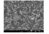
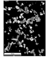
- FIG. 6 is a diagram showing an SEM image of ⁇ -sialon of Example 2.
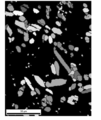
- FIG. 6 is a diagram showing an EBSD image of ⁇ -sialon of Example 2.
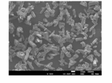
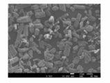
- FIG. 6 is a view showing an SEM image of ⁇ -sialon of Example 3.
- FIG. 6 is a view showing an SEM image of ⁇ -sialon of Example 3.
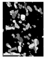
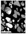
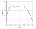
- FIG. 4 is a diagram showing an EBSD image of an ⁇ -type sialon of Example 3. It is a figure which shows the excitation spectrum when the fluorescence intensity of wavelength 598nm of the fluorescent substance which concerns on Example 3 is measured.
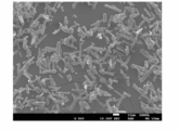
- 5 is a view showing an SEM image of ⁇ -sialon of Comparative Example 1.
- FIG. It is a figure which shows the EBSD image of the alpha sialon of the comparative example 1.
- the ⁇ -sialon according to the embodiment of the present invention has a general formula: (M) x (Eu) y (Si) 12- (m + n) (Al) m + n (O) n (N) 16-n (where M is An ⁇ -sialon represented by Li, Mg, Ca, Y and a lanthanide element (one or more elements including at least Ca selected from the group consisting of La and Ce), and 50 primary particles of ⁇ -sialon % Area average diameter is 5 ⁇ m or more.
- the solid solution composition of ⁇ -type sialon is represented by m and n determined by x and y in the above general formula and the accompanying Si / Al ratio and O / N ratio.
- ⁇ -sialon is stabilized in a wide composition range, and a part of the ⁇ -sialon is substituted with Eu serving as a light emission center, thereby being excited by light in a wide wavelength range from ultraviolet to blue. A phosphor showing orange visible emission is obtained.
- the crystal phase of ⁇ -sialon is preferably an ⁇ -sialon single phase, and may include ⁇ -sialon, aluminum nitride or polytypoids thereof as other crystal phases.
- a method for producing ⁇ -sialon there is a method in which a mixed powder comprising a compound of silicon nitride, aluminum nitride and an intruding solid solution element is heated and reacted in a high-temperature nitrogen atmosphere. Part of the constituent components forms a liquid phase in the heating step, and the substance moves to this liquid phase, thereby generating an ⁇ -sialon solid solution.
- a plurality of equiaxed primary particles are sintered to form massive secondary particles.
- the primary particles in the present invention are the smallest particles that have the same crystal orientation in the particles and can exist independently.
- the present inventors examined the relationship between the light emission characteristics and the particle properties, and the 50% area average diameter or 10% area average diameter of the primary particles of ⁇ -sialon (hereinafter, these are collectively referred to as area average diameter). As a result, the inventors have obtained the knowledge that the emission intensity can be controlled by the above, and have reached the present invention.
- ⁇ -sialon primary particles that is, single crystal particles
- primary particles means all single crystal particles, and a plurality of primary particles are sintered through grain boundaries to form secondary particles, and secondary particles are formed. Including without distinction.
- C A1 + C A2 + C A3 +... + C Ai +... + C Ak the cumulative curve is determined, 10% and 50% of this cumulative curve.
- the primary particle diameters calculated from the cross-sectional areas (s 10 , s 50 ) of the primary particles at the corresponding points are taken as the 10% area average diameter and 50% area average diameter of the primary particles, respectively.
- the area average diameter of the secondary particles of ⁇ -sialon can also be explained in the same manner as described above. That is, secondary particles formed by sintering primary particles of ⁇ -sialon are C B1 , C B2 , C B3 ,..., C Bi ,. Suppose that there is a group of secondary particles arranged as follows. When the cumulative curve was determined with the total cross-sectional area of the group of secondary particles (C B1 + C B2 + C B3 +... + C Bi +... + C Bk ) being 100%, 10% and 50% of this cumulative curve.
- the secondary particle diameter calculated from the cross-sectional area (S 10 , S 50 ) of the secondary particle at the point corresponding to% is defined as a 10% area average diameter and a 50% area average diameter of the secondary particle diameter, respectively.
- FIG. 1 is a schematic diagram showing a configuration of an apparatus used for measurement by the EBSD method.
- an apparatus 1 used for the EBSD method is composed of an apparatus in which an electron backscatter diffraction image measurement apparatus 3 is added to a scanning electron microscope 2.
- the scanning electron microscope 2 includes a lens barrel portion 2A, a stage portion 2B on which a sample 4 is placed, a stage control portion 2C, an electron beam scanning portion 2D, a control computer 2E, and the like.
- the electron backscatter diffraction image measurement apparatus 3 includes a fluorescent screen 7 that detects electrons 6 generated by irradiating a sample 4 with an electron beam 5 and scattered backward, and a camera 8 that captures a fluorescent image of the fluorescent screen 7. And software for acquiring and analyzing data of an electron backscatter diffraction image (not shown).
- the ⁇ -sialon which is the sample 4 is irradiated with an electron beam to cause electron scattering corresponding to the crystal structure and crystal plane, and the shape of this electron scattering pattern is analyzed by software. More specifically, the crystal orientation in each phosphor particle is identified, and the cross-sectional area of primary particles that can be distinguished for each crystal orientation is obtained by image analysis. At this time, the cross-sectional area of secondary particles obtained by sintering a plurality of primary particles through grain boundaries is further determined using the same EBSD image from which the area average diameter of the primary particles was calculated.
- a cumulative curve is created as described above, and the cross-sectional areas S 10 and S 50 of secondary particles at points corresponding to 10% and 50% are obtained, and using these, the following formula ( From 3) and (4), the 10% area average diameter and 50% area average diameter of the secondary particles corresponding to the diameter when converted into a circle are calculated.
- 10% area average diameter of secondary particles 2 ⁇ (S 10 / ⁇ ) 1/2
- 50% area average diameter of secondary particles 2 ⁇ (S 50 / ⁇ ) 1/2 (4)
- the 50% area average diameter of the primary particles of the present invention is 5 ⁇ m or more. Further, the larger the ratio of the 50% area average diameter of the primary particles to the 50% area average diameter of the secondary particles, the smaller the ratio of the grain interface area between the primary particles in the secondary particles, and the higher the luminous efficiency.
- the ratio of the 50% area average diameter of the primary particles to the 50% area average diameter of the preferred secondary particles is 0.56 or more.
- the ratio of the number of primary particles to the number of secondary particles is obtained by counting the number of secondary particles in the ⁇ -sialon image obtained by the EBSD method and the number of primary particles constituting the secondary particles. It is calculated by taking the ratio of the number of primary particles to the number.
- the average number of primary particles in the secondary particles is preferably 2.5 or less.
- Control of the area average diameter of the primary particles can be performed by the composition of the raw material powder, the particle size and addition amount of the pre-synthesized ⁇ -sialon powder to be added to the raw material powder, the heat treatment conditions, the pulverization conditions of the composite, etc. it can.
- the upper limit of the area average diameter of the primary particles is naturally determined according to the upper limit of the size of the secondary particles described later.
- the D50 particle size of the ⁇ -sialon secondary particles may be 13 ⁇ m or more and 30 ⁇ m or less.
- D50 is a 50% particle diameter (50% volume average diameter) in the volume-based integrated fraction.
- the D50 particle size of the ⁇ -sialon secondary particles is preferably 30 ⁇ m or less, and particularly preferably 20 ⁇ m or less.
- the D50 particle size of the ⁇ -sialon secondary particles is preferably 13 ⁇ m or more.
- the control of the D50 particle size of the ⁇ -sialon secondary particles can be performed by pulverization or classification, or in a step of removing secondary particles that are placed in water and have a small particle size and are difficult to settle.
- the ⁇ -sialon of the present invention is particularly efficiently excited by near ultraviolet to blue light and exhibits emission characteristics having a peak in the wavelength range of 590 to 630 nm. Excellent as yellow to orange phosphor. For this reason, the ⁇ -sialon of the present invention can be suitably used for various light-emitting elements, particularly white LEDs that use ultraviolet LED chips or blue LED chips as light sources, alone or in combination with other phosphors.
- ⁇ -sialon The method for producing ⁇ -sialon according to the present invention will be described.
- a part of the raw material powder reacts to form a liquid phase, and each element moves through the liquid phase, so that solid solution formation and grain growth proceed.
- ⁇ -sialon having a low oxygen content synthesized using calcium nitride as a calcium raw material can dissolve calcium at a high concentration.
- a phosphor having an emission peak wavelength on the higher wavelength side (590 nm or more) than the conventional composition using an oxide raw material is obtained.
- x + y> 1.5 is preferable.
- a part of Ca can be replaced with Li, Mg, Y, and lanthanide elements (excluding La and Ce), and the emission spectrum can be finely adjusted.
- Other raw material powders include silicon nitride, aluminum nitride, and Eu compounds.
- Examples of the Eu compound include europium oxide, a compound that becomes europium oxide after heating, and europium nitride, and preferably europium nitride that can reduce the amount of oxygen in the system.
- each raw material described above there are a dry mixing method and a method of removing the solvent after wet mixing in an inert solvent that does not substantially react with each raw material component.
- the mixing apparatus include a V-type mixer, a rocking mixer, a ball mill, and a vibration mill.
- Mixing of calcium nitride that is unstable in the atmosphere is preferably performed in a glove box in an inert atmosphere because hydrolysis and oxidation affect the properties of the synthesized product.
- the powder obtained by mixing (hereinafter simply referred to as raw material powder) is filled in a container made of a material having low reactivity with the raw material and the phosphor to be synthesized, for example, a boron nitride container, and 1650 to 1850 in a nitrogen atmosphere.
- the ⁇ -sialon phosphor is obtained by heating for a predetermined time in a temperature range of ° C.
- the temperature of the heat treatment By setting the temperature of the heat treatment to 1650 ° C. or higher, the amount of unreacted product remaining can be suppressed, and primary particles can be sufficiently grown. Suppression can be suppressed.
- the filling of the raw material powder into the container is preferably bulky from the viewpoint of suppressing interparticle sintering during heating. Specifically, it is preferable that the bulk density is 0.6 g / cm 3 or less when filling the raw material powder container.
- the heating time in the heat treatment is 2 hours or more and 24 hours or less as a time range in which there are no inconveniences such as a large amount of unreacted substances, insufficient growth of primary particles, or sintering between particles. Is preferred.
- the ⁇ -sialon whose outer shape is ingot shape is generated by the above-mentioned process.
- the ingot-shaped ⁇ -sialon is subjected to a pulverization process by a crusher such as a crusher, a mortar pulverizer, a ball mill, a vibration mill, a jet mill or the like, and a sieve classification process after these pulverization treatments, so that the D50 particle size of the secondary particles is reduced.
- An adjusted ⁇ -sialon powder is obtained.
- the D50 particle size of the secondary particles can be adjusted by performing the step of removing the secondary particles which are dispersed in an aqueous solution and have a small particle size and are difficult to settle.
- FIG. 2 is a cross-sectional view schematically showing the structure of the light-emitting device 10 of the present invention using ⁇ -sialon.
- the light emitting device 10 of the present invention includes an LED chip as the light source 12, a first lead frame 13 on which the light source 12 is mounted, a second lead frame 14, and the light source 12.
- a wavelength conversion member 15 to be covered, a bonding wire 16 that electrically connects the light emitting light source 12 and the second lead frame 14, and a synthetic resin cap 19 that covers them are formed.
- the wavelength conversion member 15 includes a phosphor 18 and a sealing resin 17 that disperses the phosphor 18.
- a concave portion 13b for mounting a light emitting diode chip as the light emitting light source 12 is formed on the upper portion 13a of the first lead frame 13.
- the concave portion 13b has a substantially funnel shape in which the hole diameter gradually increases upward from the bottom surface, and the inner surface of the concave portion 13b is a reflecting surface.
- An electrode on the lower surface side of the light emitting light source 12 is die-bonded to the bottom surface of the reflecting surface.
- the other electrode formed on the upper surface of the light emission source 12 is connected to the surface of the second lead frame 14 via the bonding wire 16.
- LED chips As the light source 12, various LED chips can be used, and an LED chip that emits light having a wavelength of 300 nm to 500 nm as a wavelength of near ultraviolet to blue light is particularly preferable.
- ⁇ -sialon As the phosphor 18 used for the wavelength conversion member 15 of the light emitting device 1, in addition to ⁇ -sialon according to the present invention, ⁇ -sialon, CaAlSiN 3 , YAG in which europium, cerium, strontium, and calcium are solid solution, or a mixture thereof.
- the body can be used. By using these together, the light wavelength of the light emitting device 10 can be controlled.
- the ⁇ -sialon of the present invention has yellow to orange emission characteristics having a peak in a wavelength range of 590 nm to 630 nm by irradiating near ultraviolet light or visible light having a wavelength of 300 nm to 500 nm as an excitation source. . Therefore, a near-ultraviolet LED chip or a blue LED chip is used as the light emitting light source 12, and the ⁇ -sialon of the present invention or the ⁇ -sialon of the present invention is used as the phosphor 18, and the red light-emitting phosphor having a wavelength of 600 nm to 700 nm.
- White light can be obtained by using a blue light emitting phosphor or a green light emitting phosphor alone or in combination.
- the emission color of the light emitting device 10 in the present invention can be changed to a color other than white light such as a light bulb color by adjusting the emission wavelength and the mixing ratio of the phosphor blended as the phosphor 18.
- the light-emitting device 10 of the present invention has high emission intensity because the ⁇ -sialon used as the phosphor 18 has high emission efficiency.
- ⁇ -type sialon As composition of the raw material powder, ⁇ -type silicon nitride powder (NP400 grade manufactured by Denki Kagaku Kogyo Co., Ltd.) 53.4% by mass, aluminum nitride powder (F grade manufactured by Tokuyama Co., Ltd.) 19.3% by mass, europium oxide powder (Shin-Etsu) RU grade manufactured by Chemical Industry Co., Ltd.) 0.9% by mass, pre-synthesized ⁇ -sialon-added powder with secondary particle D50 of 12.1 ⁇ m is 15.0% by weight, and a rocking mixer (Aichi Electric Co., Ltd.) Using RM-10), 60 minutes of dry mixing, a stainless steel sieve having an opening of 150 ⁇ m was passed through to obtain a premixed powder.
- NP400 grade manufactured by Denki Kagaku Kogyo Co., Ltd. 53.4% by mass
- aluminum nitride powder F grade manufactured by Tokuyama Co., Ltd.
- the pre-mixed powder was put in a glove box under a nitrogen atmosphere and mixed with calcium nitride powder manufactured by High Purity Chemical Laboratory.
- a raw material mixed powder was obtained through a stainless steel sieve having an opening of 250 ⁇ m, and then 120 g of the raw material mixed powder was added to a cylindrical boron nitride container with a lid having an internal volume of 0.4 liter ( N-1 grade manufactured by Denki Kagaku Kogyo Co., Ltd.).
- This raw material mixed powder was heat-treated at 1800 ° C. for 16 hours in an atmospheric pressure nitrogen atmosphere in an electric furnace of a carbon heater together with the container. Since calcium nitride contained in the raw material mixed powder is easily hydrolyzed in the air, the boron nitride container filled with the raw material mixed powder is taken out of the glove box and immediately set in an electric furnace and immediately evacuated. The reaction of calcium nitride was prevented.
- the composite was lightly crushed with a mortar and passed through a sieve having an opening of 150 ⁇ m to obtain phosphor powder.
- XRD measurement powder X-ray diffraction measurement
- the 10% area average diameter and 50% area average diameter of the primary particles of the ⁇ -sialon of Example 1 were measured using the EBSD method.
- As an EBSD method measurement was performed using a scanning electron microscope (FE-SEM, JSM-7001F type manufactured by JEOL Ltd.) 2 and an electron backscatter diffraction image measurement device (OIM device manufactured by EDAX-TSL) 3 added thereto. did.
- Example 1 the ⁇ -sialon of Example 1 is irradiated with an electron beam to cause scattering corresponding to the crystal structure and crystal orientation, and the shape of this scattering pattern is defined by software (OIM, manufactured by EDAX-TSL, Inc.). Analysis by Ver5.2) was used to identify the crystal orientation in the individual phosphor particles. Furthermore, image analysis of the particle shape in each crystal orientation, from the above formulas (1) to (4), 10% area average diameter of primary particles, 50% area average diameter, and 10% area average diameter of secondary particles, The 50% area average diameter was calculated. Furthermore, the average number of primary particles in the secondary particles was calculated from the obtained image.
- the EBSD image of FIG. 4 is prepared from the ⁇ -sialon of Example 1 shown in the scanning electron microscope image of FIG. 3 (SEM image, electron acceleration voltage is 15 kV, magnification is 500 times). Was done by.
- SEM image electron acceleration voltage is 15 kV, magnification is 500 times.
- magnification is 500 times.
- FIG. 4 the same portion of the crystal orientation is shown as a single color region, and this single color region corresponds to the primary particles.
- Statistical analysis accuracy improves as the number of primary particles to be analyzed increases. If the number of primary particles is 3000 or more, sufficient data for analysis can be obtained.
- Table 1 the 50% area average diameter and 10% area average diameter of the primary particles of ⁇ -sialon of Example 1 obtained by this image analysis were 5.7 ⁇ m and 3.0 ⁇ m, respectively.
- the ratio of the 50% area average diameter of the primary particles to the 50% area average diameter of the secondary particles and the ratio of the 10% area average diameter of the primary particles to the 10% area average diameter of the secondary particles are 0.60 and 0.00 respectively. 68, and the average number of primary particles in the secondary particles was 2.0.
- D50 The particle size distribution of the secondary particles of the ⁇ -sialon of Example 1 was measured by a laser diffraction scattering method to determine D50. D50 of the ⁇ -type sialon of Example 1 was 13.5 ⁇ m.
- Example 1 (Peak emission wavelength) The ⁇ -sialon of Example 1 was filled so that the surface of the concave cell was smooth, and an integrating sphere was attached. Monochromatic light separated into a wavelength of 455 nm from a light emitting light source (Xe lamp) was introduced into the integrating sphere using an optical fiber. Using this monochromatic light as an excitation source, ⁇ -sialon was irradiated, and a spectrophotometer (MCPD-7000, manufactured by Otsuka Electronics Co., Ltd.) was used to measure the fluorescence spectrum of the sample, and the emission peak wavelength was determined. As shown in Table 1, the emission peak wavelength was 597 nm as shown in Table 1.
- MCPD-7000 spectrophotometer
- Example 2 The blending composition of the ⁇ -sialon raw material powder of Example 2 is 44.0% by mass ⁇ -type silicon nitride powder, 15.9% by mass aluminum nitride powder, 0.8% by mass europium oxide powder, and D50 of secondary particles.
- a premixed powder containing 30.0% by weight of a pre-synthesized ⁇ -sialon-added powder of 13.5 ⁇ m, and further mixing ratio (mass ratio) of the premixed powder and calcium nitride powder in a glove box under a nitrogen atmosphere 90.7:
- the mixture was 9.3.
- About the grades of the raw material powder other than the ⁇ -type sialon-added powder, the same as in Example 1 was used.
- the ⁇ -sialon of Example 2 was produced in the same manner as in Example 1 except for these conditions.
- FIG. 5 shows an SEM image of the ⁇ -type sialon of Example 2.
- An EBSD image is shown in FIG.
- the 50% area average diameter and 10% area average diameter of the primary particles of ⁇ -sialon of Example 2 were calculated, and as shown in Table 1, they were 7.7 ⁇ m and 4.0 ⁇ m, respectively. It was.
- the ratio of the 50% area average diameter of the primary particles to the 50% area average diameter of the secondary particles and the ratio of the 10% area average diameter of the primary particles to the 10% area average diameter of the secondary particles are 0.57 and 0.00 respectively. 66, and the average number of primary particles in the secondary particles was 2.0.
- the luminous efficiency and peak wavelength were 69.1% and 596 nm as shown in Table 1.
- Example 3 The composition of the ⁇ -sialon raw material powder of Example 3 is 56.6% by mass of ⁇ -type silicon nitride powder, 20.4% by mass of aluminum nitride powder, 1.0% by mass of europium oxide powder, and secondary particles.
- the premixed ⁇ -sialon-added powder having a D50 of 19.4 ⁇ m and a premixed powder containing 10.0% by weight was further mixed in a glove box under a nitrogen atmosphere. 88.0: 12.0 mass ratio was mixed. About the raw material powder other than the ⁇ -type sialon-added powder, the same powder as in Examples 1 and 2 was used.
- Example 2 the composite was obtained. Thereafter, the composite was pulverized with a supersonic jet pulverizer (PJM-80 type, manufactured by Nippon Pneumatic Industry Co., Ltd.) at a pulverization air pressure of 0.2 MPa, and passed through a sieve having an opening of 150 ⁇ m to obtain a phosphor powder.
- a supersonic jet pulverizer (PJM-80 type, manufactured by Nippon Pneumatic Industry Co., Ltd.) at a pulverization air pressure of 0.2 MPa
- FIG. 7 shows an SEM image of the ⁇ -type sialon of Example 3.
- An EBSD image is shown in FIG.
- Example 1 and Example 2 the 50% area average diameter and 10% area average diameter of the primary particles of the ⁇ -sialon of Example 3 were calculated, and as shown in Table 1, 11.7 ⁇ m and 5%, respectively. .8 ⁇ m.
- the ratio of the 50% area average diameter of the primary particles to the 50% area average diameter of the secondary particles and the ratio of the 10% area average diameter of the primary particles to the 10% area average diameter of the secondary particles are 0.63 and 0.00 respectively. 81, and the average number of primary particles in the secondary particles was 2.1.
- D50 was 14.1 ⁇ m as shown in Table 1.
- the luminous efficiency and the peak wavelength were 66.5% and 598 nm as shown in Table 1.
- the excitation spectrum of the ⁇ -sialon of Example 3 was measured using the spectrofluorometer described above.
- FIG. 9 shows an excitation spectrum when the fluorescence intensity of the phosphor of Example 3 having a wavelength of 598 nm is measured.
- the phosphor of the present invention is excited in a wide wavelength range from ultraviolet to visible. In particular, since it is efficiently excited at a wavelength of 300 to 500 nm, it is suitable for a light emitting device using near ultraviolet and blue LEDs as excitation sources.
- Comparative Example 1 The ⁇ -sialon of Comparative Example 1 was used in the same composition as the ⁇ -sialon raw material powder of Example 1 except that a pre-synthesized ⁇ -sialon-added powder having a secondary particle D50 of 10.4 ⁇ m was used. Produced.
- FIG. 10 shows an SEM image of ⁇ -sialon of Comparative Example 1.
- An EBSD image is shown in FIG.
- the 50% area average diameter and the 10% area average diameter of the primary particles of ⁇ -sialon of Comparative Example 1 were calculated.
- the average particle diameter was 4.8 ⁇ m and 2.7 ⁇ m. there were.
- the ratio of the 50% area average diameter of the primary particles to the 50% area average diameter of the secondary particles and the ratio of the 10% area average diameter of the primary particles to the 10% area average diameter of the secondary particles are 0.55 and 0.00 respectively.
- the average number of primary particles in the secondary particles was 2.6.
- Example 4 When the composite obtained after the heat treatment of Example 3 is pulverized by a supersonic jet pulverizer, the pulverization air pressure is pulverized at 0.15 MPa lower than that of Example 3, and a sieve having an opening of 150 ⁇ m is passed through all. A phosphor powder was obtained.
- the ⁇ -sialon of Example 4 has a 50% area average diameter of primary particles of 5 ⁇ m or more, but the ratio of the 50% area average diameter of primary particles to the 50% area average diameter of secondary particles of ⁇ -sialon is 0. This is an example of less than .56.
- the luminous efficiency and peak wavelength of the phosphor 18 of Example 4 were 64.2% and 598 nm.
- the phosphor 18 is a mixture of ⁇ -sialon of Example 3 and ⁇ -sialon: Eu phosphor having a composition of Si 5.75 A 0.25 O 0.25 N 7.75 : Eu.
- the emission peak wavelength of ⁇ -sialon: Eu phosphor was 543 nm, and the luminous efficiency of this phosphor when excited at 450 nm was 54%.
- the phosphor 18 was blended into the sealing resin 17 as follows.
- the phosphor 18 is individually treated in advance with a silane coupling agent (KBE402 manufactured by Shin-Etsu Silicone), and the phosphor 18 subjected to the silane coupling treatment is used as an epoxy resin (NLD-SL manufactured by Sanyu Rec). -2101) to complete.
- a blue LED chip having an emission wavelength of 450 nm was used as the light emission source 12.
- ⁇ Comparative Example 2> The light emitting device of Comparative Example 2 is the same as Example 5 except that the ⁇ type sialon of Example 3 used as the phosphor 18 in the light emitting device 10 of Example 5 is changed to the ⁇ type sialon of Comparative Example 1. Produced.
- Example 5 The light emitting device 10 of Example 5 and the light emitting device of Comparative Example 2 were allowed to emit light under the same conditions, and the central illuminance and CIE chromaticity (CIE 1931) under the same conditions were measured with a luminance meter.
- CIE 1931 CIE chromaticity
- Example 5 was 1.22 times as bright as Comparative Example 2.
Landscapes
- Chemical & Material Sciences (AREA)
- Organic Chemistry (AREA)
- Inorganic Chemistry (AREA)
- Engineering & Computer Science (AREA)
- Materials Engineering (AREA)
- Luminescent Compositions (AREA)
- Led Device Packages (AREA)
Abstract
Description
(α型サイアロン)
本発明の実施形態に係るα型サイアロンは、一般式:(M)x(Eu)y(Si)12-(m+n)(Al)m+n(O)n(N)16-n(ただし、MはLi、Mg、Ca、Y及びランタニド元素(LaとCeを除く)からなる群から選ばれる少なくともCaを含む1種以上の元素)で示されるα型サイアロンであり、α型サイアロンの一次粒子の50%面積平均径が5μm以上である。
一次粒子の10%面積平均径=2×(s10/π)1/2 (1)
一次粒子の50%面積平均径=2×(s50/π)1/2 (2)
同様に、得られた断面積から、上記のように累積カーブを作成し、10%、50%にあたる点の二次粒子の断面積S10、S50を求め、これらを用いて、下式(3)、(4)から、円換算した場合の直径にあたる二次粒子の10%面積平均径及び50%面積平均径を算出する。
二次粒子の10%面積平均径=2×(S10/π)1/2 (3)
二次粒子の50%面積平均径=2×(S50/π)1/2 (4)
本発明のα型サイアロンの製造方法について説明する。α型サイアロンは、合成過程において、主として原料粉末の一部が反応して液相が形成し、その液相を介して各元素が移動することにより、固溶体形成と粒成長が進む。カルシウム原料として、窒化カルシウムを使用して合成した酸素含有率の低いα型サイアロンは、高濃度のカルシウムの固溶ができる。特にCa固溶濃度が高い場合、酸化物原料を使用した従来組成よりも高波長側(590nm以上)に発光ピーク波長を有する蛍光体が得られる。具体的には前記一般式において、x+y>1.5が好ましい。Caの一部をLi、Mg、Y及びランタニド元素(LaとCeを除く。)に置換し、発光スペクトルの微調整を行うこともできる。
本発明の実施形態に係る発光装置について、図2を参照しながら説明する。図2は、α型サイアロンを用いた本発明の発光装置10の構造を模式的に示す断面図である。図2に示すように、本発明の発光装置10は、発光光源12としてのLEDチップと、発光光源12を搭載する第1のリードフレーム13と、第2のリードフレーム14と、発光光源12を被覆する波長変換部材15と、発光光源12と第2のリードフレーム14を電気的につなぐボンディングワイヤ16と、これらを覆う合成樹脂製のキャップ19で形成されている。波長変換部材15は、蛍光体18と、蛍光体18を分散する封止樹脂17とを有する。

(α型サイアロンの合成)
原料粉末の配合組成として、α型窒化ケイ素粉末(電気化学工業株式会社製NP400グレード)53.4質量%、窒化アルミニウム粉末(トクヤマ株式会社製Fグレード)19.3質量%、酸化ユーロピウム粉末(信越化学工業社製RUグレード)0.9質量%、二次粒子のD50が12.1μmの予め合成したα型サイアロン添加粉末を15.0重量%とし、これらの混合物に対してロッキングミキサー(愛知電機社製RM-10)を用い、60分間乾式で混合した後、目開き150μmのステンレス製篩を全通させ、予備混合粉末を得た。
実施例1のα型サイアロンの一次粒子の10%面積平均径、及び50%面積平均径を、EBSD法を用いて測定した。EBSD法として、走査型電子顕微鏡(日本電子社製FE-SEM、JSM-7001F型)2に電子後方散乱回折像法測定装置(EDAX-TSL社製OIM装置)3を付加した装置を用いて測定した。
加速電圧:15kV
作動距離:15mm
試料傾斜角度:70°
測定領域:80μm×200μm
ステップ幅:0.2μm
測定時間:50msec/ステップ
データポイント数:約400,000ポイント
画像解析にあっては、図3の走査型電子顕微鏡像(SEM像、電子の加速電圧は15kV、倍率は500倍)に示す実施例1のα型サイアロンから、図4のEBSD像を作製することによって行った。図4において、結晶方位の同じ部分が単一色領域で示されており、この単一色領域が一次粒子に相当する。解析の対象とする一次粒子の数が多いほど統計的な解析精度が向上する。一次粒子の数が3000個以上であれば解析に十分なデータが得られる。この画像解析により求めた実施例1のα型サイアロンの一次粒子の50%面積平均径及び10%面積平均径は、表1に示すように、それぞれ5.7μm及び3.0μmであった。二次粒子の50%面積平均径に対する一次粒子の50%面積平均径の比及び二次粒子の10%面積平均径に対する一次粒子の10%面積平均径の比は、それぞれ0.60及び0.68であり、二次粒子中における一次粒子の平均個数は2.0であった。
実施例1のα型サイアロンの二次粒子の粒度分布をレーザー回折散乱法によって測定し、D50を求めた。実施例1のα型サイアロンのD50は、13.5μmであった。
凹型のセルの表面が平滑になるように実施例1のα型サイアロンを充填し、積分球を取り付けた。この積分球に、発光光源(Xeランプ)から455nmの波長に分光した単色光を、光ファイバーを用いて導入した。この単色光を励起源として、α型サイアロンに照射し、分光光度計(大塚電子社製、MCPD-7000)を用いて、試料の蛍光スペクトル測定を行ない、発光ピーク波長を求めた。発光ピーク波長は実施例1のピーク波長は、表1に示すように、597nmであった。
同じ測定器を用い、反射率が99%の標準反射板(Labsphere社製、商品名「スペクトラロン」)を試料部にセットし、波長455nmの励起光のスペクトルを測定した。その際、450~465nmの波長範囲のスペクトルから励起光フォトン数(Qex)を算出した。次いで、α型サイアロンを試料部にセットし、得られたスペクトルデータから発光フォトン数(Qem)を算出した。発光フォトン数は、465~800nmの範囲で算出した。得られた三種類のフォトン数から発光効率(=Qem/Qex×100)を求めた。波長455nmの青色光で励起した場合の発光効率は、66.6%であった。
実施例2のα型サイアロンの原料粉末の配合組成として、α型窒化ケイ素粉末44.0質量%、窒化アルミニウム粉末15.9質量%、酸化ユーロピウム粉末0.8質量%、二次粒子のD50が13.5μmの予め合成したα型サイアロン添加粉末を30.0重量%とする予備混合粉末を用い、さらに窒素雰囲気下のグローブボックス内で、予備混合粉末と窒化カルシウム粉末の混合比(質量比)=90.7:9.3で混合した。α型サイアロン添加粉末以外の原料粉末のグレードについては、実施例1と同じものを用いた。これら以外の条件は、実施例1と同様にして実施例2のα型サイアロンを作製した。
実施例3のα型サイアロンの原料粉末の配合組成として、α型窒化ケイ素粉末を56.6質量%、窒化アルミニウム粉末を20.4質量%、酸化ユーロピウム粉末を1.0質量%、二次粒子のD50が19.4μmの予め合成したα型サイアロン添加粉末を10.0重量%とする予備混合粉末を用い、さらに窒素雰囲気下のグローブボックス内で、予備混合粉末と窒化カルシウム粉末の混合比=88.0:12.0質量比で混合した。α型サイアロン添加粉末以外の原料粉末については、実施例1及び2と同じものを用いた。そして、実施例1及び2と同様にして、窒化ホウ素製容器に充填後、電気炉で加熱処理を行い、合成物を得た。その後、合成物を超音速ジェット粉砕機(日本ニューマチック工業社製PJM―80型)により粉砕エアー圧力0.2MPaで粉砕し、目開き150μmの篩を全通させ、蛍光体粉末を得た。
二次粒子のD50が10.4μmである予め合成したα型サイアロン添加粉末を用いたこと以外は、実施例1のα型サイアロンの原料粉末と同じ配合組成として、比較例1のα型サイアロンを作製した。
実施例3の加熱処理後に得られた合成物を超音速ジェット粉砕機により粉砕する際、粉砕エアー圧力を、実施例3より低い0.15MPaで粉砕し、目開き150μmの篩を全通させ、蛍光体粉末を得た。実施例4のα型サイアロンは、一次粒子の50%面積平均径が5μm以上であるが、α型サイアロンの二次粒子の50%面積平均径に対する一次粒子の50%面積平均径の比が0.56未満の例である。実施例4の蛍光体18の発光効率及びピーク波長は、表1に示すように、64.2%、598nmであった。
α型サイアロンを用いた発光装置の例を、図2を参照して詳細に説明する。蛍光体18は、実施例3のα型サイアロンと、Si5.75A0.25O0.25N7.75:Euの組成を持つβ型サイアロン:Eu蛍光体の混合体である。β型サイアロン:Eu蛍光体の発光ピーク波長は543nmであり、この蛍光体の450nm励起での発光効率は54%であった。
発光光源12としては、発光波長450nmの青色LEDチップを用いた。
比較例2の発光装置は、実施例5の発光装置10において、蛍光体18として用いた実施例3のα型サイアロンを比較例1のα型サイアロンに変更した以外は、実施例5と同様に作製した。
2:走査型電子顕微鏡
2A:鏡筒部
2B:ステージ部
2C:ステージ制御部
2D:電子線走査部
2E:制御用コンピュータ
3:電子後方散乱回折像法測定装置
4:試料
5:電子線
6:後方散乱された電子
7:蛍光スクリーン
8:カメラ
10:発光装置
12:発光光源(LEDチップ)
13:第1のリードフレーム
13a:上部
13b:凹部
14:第2のリードフレーム
15:波長変換部材
16:ボンディングワイヤ
17:封止樹脂
18:蛍光体(α型サイアロン)
19:キャップ
Claims (14)
- 一般式:(M)x(Eu)y(Si)12-(m+n)(Al)m+n(O)n(N)16-n(ただし、MはLi、Mg、Ca、Y及びランタニド元素(LaとCeを除く)からなる群から選ばれる少なくともCaを含む1種以上の元素)で示されるα型サイアロンであり、前記α型サイアロンの一次粒子の50%面積平均径が5μm以上であるα型サイアロン。
- 前記α型サイアロンの二次粒子の50%面積平均径に対する一次粒子の50%面積平均径の比が0.56以上である請求項1に記載のα型サイアロン。
- 前記α型サイアロンの二次粒子中における一次粒子の平均個数が2.5以下である請求項1又は2に記載のα型サイアロン。
- 前記α型サイアロンの一次粒子の10%面積平均径が3μm以上である請求項1乃至3のいずれか一項に記載のα型サイアロン。
- 前記α型サイアロンの二次粒子の10%面積平均径に対する一次粒子の10%面積平均径の比が0.65以上である請求項4に記載のα型サイアロン。
- 前記α型サイアロンの二次粒子のD50粒径(50%体積平均径)が13μm以上30μm以下である請求項1乃至5のいずれか一項に記載のα型サイアロン。
- 発光光源と波長変換部材とを含む発光装置であって、前記波長変換部材は蛍光体を含み、前記蛍光体が請求項1乃至6のいずれか一項に記載のα型サイアロンである発光装置。
- 前記蛍光体が、さらにEu固溶β型サイアロンを含む請求項7記載の発光装置。
- 前記蛍光体が、さらにEu固溶β型サイアロン、及び、CaAlSiN3を含む請求項7記載の発光装置。
- 前記発光光源が、300nm~500nmの波長の光を発生するLEDチップである請求項7乃至9のいずれか一項記載の発光装置。
- 請求項7乃至10のいずれか一項記載の発光装置を有する照明装置。
- 請求項7乃至10のいずれか一項記載の発光装置を有する信号機。
- 請求項7乃至10のいずれか一項記載の発光装置を有する液晶パネル。
- 請求項7乃至10のいずれか一項記載の発光装置を有する画像表示装置。
Priority Applications (4)
| Application Number | Priority Date | Filing Date | Title |
|---|---|---|---|
| US13/981,286 US9024519B2 (en) | 2011-01-26 | 2011-11-30 | α-SiAlON, light-emitting device and use thereof |
| KR1020137020788A KR101866600B1 (ko) | 2011-01-26 | 2011-11-30 | α 형 사이알론, 발광 장치 및 그 용도 |
| EP11857315.3A EP2669352B1 (en) | 2011-01-26 | 2011-11-30 | Alpha-sialon, light-emitting device and use thereof |
| JP2012554628A JP5778699B2 (ja) | 2011-01-26 | 2011-11-30 | α型サイアロン、発光装置及びその用途 |
Applications Claiming Priority (2)
| Application Number | Priority Date | Filing Date | Title |
|---|---|---|---|
| JP2011014269 | 2011-01-26 | ||
| JP2011-014269 | 2011-01-26 |
Publications (1)
| Publication Number | Publication Date |
|---|---|
| WO2012101899A1 true WO2012101899A1 (ja) | 2012-08-02 |
Family
ID=46558493
Family Applications (1)
| Application Number | Title | Priority Date | Filing Date |
|---|---|---|---|
| PCT/JP2011/077606 Ceased WO2012101899A1 (ja) | 2011-01-26 | 2011-11-30 | α型サイアロン、発光装置及びその用途 |
Country Status (7)
| Country | Link |
|---|---|
| US (1) | US9024519B2 (ja) |
| EP (1) | EP2669352B1 (ja) |
| JP (1) | JP5778699B2 (ja) |
| KR (1) | KR101866600B1 (ja) |
| CN (1) | CN102618276B (ja) |
| TW (1) | TWI518029B (ja) |
| WO (1) | WO2012101899A1 (ja) |
Cited By (4)
| Publication number | Priority date | Publication date | Assignee | Title |
|---|---|---|---|---|
| JP2014216445A (ja) * | 2013-04-25 | 2014-11-17 | 株式会社小糸製作所 | 発光装置 |
| JPWO2014077132A1 (ja) * | 2012-11-13 | 2017-01-05 | デンカ株式会社 | 蛍光体、発光素子及び照明装置 |
| WO2020105456A1 (ja) * | 2018-11-19 | 2020-05-28 | デンカ株式会社 | β型サイアロン蛍光体および発光装置 |
| JP2020084177A (ja) * | 2019-10-30 | 2020-06-04 | デンカ株式会社 | β型サイアロン蛍光体および発光装置 |
Families Citing this family (11)
| Publication number | Priority date | Publication date | Assignee | Title |
|---|---|---|---|---|
| US20120313507A1 (en) * | 2010-07-20 | 2012-12-13 | Kagaku Kogyo Kabushiki Kaisha | beta-SIALON, METHOD FOR MANUFACTURING THE SAME, AND LIGHT-EMITTING DEVICE |
| CN103811637B (zh) * | 2012-11-05 | 2018-01-30 | 晶元光电股份有限公司 | 波长转换材料及其应用 |
| JP6261196B2 (ja) * | 2013-06-12 | 2018-01-17 | 信越化学工業株式会社 | 発光装置 |
| KR101476217B1 (ko) * | 2014-05-28 | 2014-12-24 | 엘지전자 주식회사 | 황색 발광 형광체 및 이를 이용한 발광 소자 패키지 |
| US11387390B2 (en) * | 2017-11-27 | 2022-07-12 | Nichia Corporation | Method for producing wavelength converting member, and wavelength converting member |
| JP2019135738A (ja) * | 2018-02-05 | 2019-08-15 | 株式会社ブイ・テクノロジー | フルカラーled表示パネル及びその製造方法 |
| CN109020558B (zh) * | 2018-09-07 | 2021-11-12 | 安徽理工大学 | 一种大功率暖白光固态照明用SiAlON荧光透明陶瓷及其制备方法 |
| JP6785333B2 (ja) * | 2019-03-29 | 2020-11-18 | デンカ株式会社 | 蛍光体粉末、複合体および発光装置 |
| JP6667027B1 (ja) * | 2019-03-29 | 2020-03-18 | デンカ株式会社 | 蛍光体粉末、複合体および発光装置 |
| DE112021000924T5 (de) * | 2020-02-07 | 2022-11-17 | Denka Company Limited | Leuchtstoffplatte und lichtemittierende Vorrichtung |
| CN112573492B (zh) * | 2020-11-24 | 2024-04-26 | 兰州冉华实德新材料有限公司 | 一种锶铕氮化物固溶体粉末及其制备方法 |
Citations (7)
| Publication number | Priority date | Publication date | Assignee | Title |
|---|---|---|---|---|
| JP2004186278A (ja) * | 2002-11-29 | 2004-07-02 | Toyoda Gosei Co Ltd | 発光装置及び発光方法 |
| JP2006041096A (ja) * | 2004-07-26 | 2006-02-09 | Nichia Chem Ind Ltd | 発光装置および蛍光体 |
| JP2006052337A (ja) * | 2004-08-12 | 2006-02-23 | Fujikura Ltd | サイアロン蛍光体およびその製造方法 |
| WO2008004640A1 (en) * | 2006-07-05 | 2008-01-10 | Ube Industries, Ltd. | Sialon-base oxynitride phosphors and process for production thereof |
| WO2008084848A1 (ja) * | 2007-01-12 | 2008-07-17 | National Institute For Materials Science | 蛍光体、その製造方法および発光器具 |
| JP2008263209A (ja) * | 2004-08-11 | 2008-10-30 | National Institute For Materials Science | 蛍光体を用いた発光器具 |
| JP2009096882A (ja) | 2007-10-17 | 2009-05-07 | Denki Kagaku Kogyo Kk | 蛍光体とその製造方法 |
Family Cites Families (13)
| Publication number | Priority date | Publication date | Assignee | Title |
|---|---|---|---|---|
| KR100900282B1 (ko) * | 2004-06-18 | 2009-05-29 | 도쿠리츠교세이호징 붓시쯔 자이료 겐큐키코 | α형 사이알론 및 α형 사이알론 형광체 및 그 제조 방법 |
| JP4888624B2 (ja) * | 2004-07-30 | 2012-02-29 | 独立行政法人物質・材料研究機構 | α型サイアロン粉末の製造方法 |
| CN101128564B (zh) * | 2005-02-28 | 2012-07-25 | 电气化学工业株式会社 | 荧光体及其制造方法及使用了该荧光体的发光元件 |
| CN102585810A (zh) * | 2005-02-28 | 2012-07-18 | 电气化学工业株式会社 | 荧光体及其制造方法及使用了该荧光体的发光元件 |
| EP1867697B1 (en) * | 2005-03-04 | 2014-05-14 | Mitsubishi Chemical Corporation | Fluorescent substance and process for producing the same, and light emitting device using said fluorescent substance |
| WO2007129713A1 (ja) | 2006-05-10 | 2007-11-15 | Denki Kagaku Kogyo Kabushiki Kaisha | サイアロン蛍光体及びその製造方法並びにそれを用いた照明器具及び発光素子 |
| JP5229770B2 (ja) | 2007-03-22 | 2013-07-03 | 株式会社フジクラ | サイアロン蛍光体 |
| US8178001B2 (en) * | 2007-04-18 | 2012-05-15 | Mitsubishi Chemical Corporation | Method for producing inorganic compound, phosphor, phosphor-containing composition, light-emitting device, lighting system, and display device |
| US8513876B2 (en) * | 2007-05-22 | 2013-08-20 | National Institute For Materials Science | Fluorescent substance, method for producing the same, and light-emitting device using the same |
| JP5578597B2 (ja) * | 2007-09-03 | 2014-08-27 | 独立行政法人物質・材料研究機構 | 蛍光体及びその製造方法、並びにそれを用いた発光装置 |
| KR101213298B1 (ko) * | 2007-10-10 | 2012-12-18 | 우베 고산 가부시키가이샤 | β-사이알론 형광체 분말 및 그 제조 방법 |
| MY158794A (en) * | 2008-08-13 | 2016-11-15 | Ube Industries | LI-CONTAINING a-SIALON-BASED PHOSPHOR, PRODUCTION PROCESS THEREOF, LIGHTING DEVICE AND IMAGE DISPLAY DEVICE |
| EP2383324A4 (en) * | 2009-01-27 | 2012-08-15 | Denki Kagaku Kogyo Kk | SINGLE-BASED LUMINOPHORE, METHOD FOR PRODUCING SAME, AND LIGHT EMITTING DEVICE |
-
2011
- 2011-11-30 JP JP2012554628A patent/JP5778699B2/ja active Active
- 2011-11-30 US US13/981,286 patent/US9024519B2/en active Active
- 2011-11-30 KR KR1020137020788A patent/KR101866600B1/ko active Active
- 2011-11-30 WO PCT/JP2011/077606 patent/WO2012101899A1/ja not_active Ceased
- 2011-11-30 EP EP11857315.3A patent/EP2669352B1/en active Active
-
2012
- 2012-01-10 TW TW101100885A patent/TWI518029B/zh active
- 2012-01-21 CN CN201210020012.1A patent/CN102618276B/zh active Active
Patent Citations (7)
| Publication number | Priority date | Publication date | Assignee | Title |
|---|---|---|---|---|
| JP2004186278A (ja) * | 2002-11-29 | 2004-07-02 | Toyoda Gosei Co Ltd | 発光装置及び発光方法 |
| JP2006041096A (ja) * | 2004-07-26 | 2006-02-09 | Nichia Chem Ind Ltd | 発光装置および蛍光体 |
| JP2008263209A (ja) * | 2004-08-11 | 2008-10-30 | National Institute For Materials Science | 蛍光体を用いた発光器具 |
| JP2006052337A (ja) * | 2004-08-12 | 2006-02-23 | Fujikura Ltd | サイアロン蛍光体およびその製造方法 |
| WO2008004640A1 (en) * | 2006-07-05 | 2008-01-10 | Ube Industries, Ltd. | Sialon-base oxynitride phosphors and process for production thereof |
| WO2008084848A1 (ja) * | 2007-01-12 | 2008-07-17 | National Institute For Materials Science | 蛍光体、その製造方法および発光器具 |
| JP2009096882A (ja) | 2007-10-17 | 2009-05-07 | Denki Kagaku Kogyo Kk | 蛍光体とその製造方法 |
Non-Patent Citations (1)
| Title |
|---|
| See also references of EP2669352A4 |
Cited By (6)
| Publication number | Priority date | Publication date | Assignee | Title |
|---|---|---|---|---|
| JPWO2014077132A1 (ja) * | 2012-11-13 | 2017-01-05 | デンカ株式会社 | 蛍光体、発光素子及び照明装置 |
| JP2014216445A (ja) * | 2013-04-25 | 2014-11-17 | 株式会社小糸製作所 | 発光装置 |
| WO2020105456A1 (ja) * | 2018-11-19 | 2020-05-28 | デンカ株式会社 | β型サイアロン蛍光体および発光装置 |
| US11702592B2 (en) | 2018-11-19 | 2023-07-18 | Denka Company Limited | B-sialon phosphor and light emitting device |
| JP2020084177A (ja) * | 2019-10-30 | 2020-06-04 | デンカ株式会社 | β型サイアロン蛍光体および発光装置 |
| JP7278924B2 (ja) | 2019-10-30 | 2023-05-22 | デンカ株式会社 | β型サイアロン蛍光体および発光装置 |
Also Published As
| Publication number | Publication date |
|---|---|
| KR20140039150A (ko) | 2014-04-01 |
| KR101866600B1 (ko) | 2018-06-11 |
| JP5778699B2 (ja) | 2015-09-16 |
| TWI518029B (zh) | 2016-01-21 |
| CN102618276B (zh) | 2014-07-02 |
| TW201235294A (en) | 2012-09-01 |
| EP2669352B1 (en) | 2018-10-10 |
| EP2669352A1 (en) | 2013-12-04 |
| EP2669352A4 (en) | 2015-06-03 |
| JPWO2012101899A1 (ja) | 2014-06-30 |
| CN102618276A (zh) | 2012-08-01 |
| US9024519B2 (en) | 2015-05-05 |
| US20130293093A1 (en) | 2013-11-07 |
Similar Documents
| Publication | Publication Date | Title |
|---|---|---|
| JP5778699B2 (ja) | α型サイアロン、発光装置及びその用途 | |
| KR101419626B1 (ko) | β형 사이알론, β형 사이알론의 제조 방법 및 발광 장치 | |
| JP7278924B2 (ja) | β型サイアロン蛍光体および発光装置 | |
| TWI829803B (zh) | β型矽鋁氮氧化物螢光體及發光裝置 | |
| WO2012033157A1 (ja) | β型サイアロン及び発光装置 | |
| WO2022102512A1 (ja) | 蛍光体粉末、発光装置、画像表示装置および照明装置 | |
| TWI833035B (zh) | β型矽鋁氮氧化物螢光體及發光裝置 | |
| JP7590449B2 (ja) | 蛍光体粉末、発光装置、画像表示装置および照明装置 | |
| TW202113034A (zh) | α型矽鋁氮氧化物螢光體、發光構件、以及發光裝置 | |
| JP7763932B2 (ja) | Eu賦活β型サイアロン蛍光体粒子、β型サイアロン蛍光体粉末および発光装置 | |
| CN113710771B (zh) | 荧光体粒子、复合体、发光装置和荧光体粒子的制造方法 | |
| KR20250085828A (ko) | 형광체 분말, 및 발광 장치 | |
| JP2012025956A (ja) | β型サイアロンの製造方法 | |
| KR20250084217A (ko) | 형광체, 및 발광 장치 | |
| CN120518398A (zh) | β型赛隆荧光体、复合体、波长转换部件、发光装置及β型赛隆荧光体的制造方法 |
Legal Events
| Date | Code | Title | Description |
|---|---|---|---|
| 121 | Ep: the epo has been informed by wipo that ep was designated in this application |
Ref document number: 11857315 Country of ref document: EP Kind code of ref document: A1 |
|
| WWE | Wipo information: entry into national phase |
Ref document number: 13981286 Country of ref document: US |
|
| ENP | Entry into the national phase |
Ref document number: 2012554628 Country of ref document: JP Kind code of ref document: A |
|
| NENP | Non-entry into the national phase |
Ref country code: DE |
|
| WWE | Wipo information: entry into national phase |
Ref document number: 2011857315 Country of ref document: EP |
|
| ENP | Entry into the national phase |
Ref document number: 20137020788 Country of ref document: KR Kind code of ref document: A |