WO2012102267A1 - 回路基板、及びそれを用いた半導体装置 - Google Patents
回路基板、及びそれを用いた半導体装置 Download PDFInfo
- Publication number
- WO2012102267A1 WO2012102267A1 PCT/JP2012/051435 JP2012051435W WO2012102267A1 WO 2012102267 A1 WO2012102267 A1 WO 2012102267A1 JP 2012051435 W JP2012051435 W JP 2012051435W WO 2012102267 A1 WO2012102267 A1 WO 2012102267A1
- Authority
- WO
- WIPO (PCT)
- Prior art keywords
- layer
- bonding
- ceramic substrate
- metal
- semiconductor device
- Prior art date
- Legal status (The legal status is an assumption and is not a legal conclusion. Google has not performed a legal analysis and makes no representation as to the accuracy of the status listed.)
- Ceased
Links
Images


Classifications
-
- H—ELECTRICITY
- H10—SEMICONDUCTOR DEVICES; ELECTRIC SOLID-STATE DEVICES NOT OTHERWISE PROVIDED FOR
- H10W—GENERIC PACKAGES, INTERCONNECTIONS, CONNECTORS OR OTHER CONSTRUCTIONAL DETAILS OF DEVICES COVERED BY CLASS H10
- H10W90/00—Package configurations
-
- C—CHEMISTRY; METALLURGY
- C04—CEMENTS; CONCRETE; ARTIFICIAL STONE; CERAMICS; REFRACTORIES
- C04B—LIME, MAGNESIA; SLAG; CEMENTS; COMPOSITIONS THEREOF, e.g. MORTARS, CONCRETE OR LIKE BUILDING MATERIALS; ARTIFICIAL STONE; CERAMICS; REFRACTORIES; TREATMENT OF NATURAL STONE
- C04B35/00—Shaped ceramic products characterised by their composition; Ceramics compositions; Processing powders of inorganic compounds preparatory to the manufacturing of ceramic products
- C04B35/622—Forming processes; Processing powders of inorganic compounds preparatory to the manufacturing of ceramic products
- C04B35/64—Burning or sintering processes
- C04B35/645—Pressure sintering
-
- C—CHEMISTRY; METALLURGY
- C04—CEMENTS; CONCRETE; ARTIFICIAL STONE; CERAMICS; REFRACTORIES
- C04B—LIME, MAGNESIA; SLAG; CEMENTS; COMPOSITIONS THEREOF, e.g. MORTARS, CONCRETE OR LIKE BUILDING MATERIALS; ARTIFICIAL STONE; CERAMICS; REFRACTORIES; TREATMENT OF NATURAL STONE
- C04B37/00—Joining burned ceramic articles with other burned ceramic articles or other articles by heating
- C04B37/02—Joining burned ceramic articles with other burned ceramic articles or other articles by heating with metallic articles
- C04B37/023—Joining burned ceramic articles with other burned ceramic articles or other articles by heating with metallic articles characterised by the interlayer used
- C04B37/025—Joining burned ceramic articles with other burned ceramic articles or other articles by heating with metallic articles characterised by the interlayer used consisting of glass or ceramic material
-
- C—CHEMISTRY; METALLURGY
- C04—CEMENTS; CONCRETE; ARTIFICIAL STONE; CERAMICS; REFRACTORIES
- C04B—LIME, MAGNESIA; SLAG; CEMENTS; COMPOSITIONS THEREOF, e.g. MORTARS, CONCRETE OR LIKE BUILDING MATERIALS; ARTIFICIAL STONE; CERAMICS; REFRACTORIES; TREATMENT OF NATURAL STONE
- C04B37/00—Joining burned ceramic articles with other burned ceramic articles or other articles by heating
- C04B37/02—Joining burned ceramic articles with other burned ceramic articles or other articles by heating with metallic articles
- C04B37/023—Joining burned ceramic articles with other burned ceramic articles or other articles by heating with metallic articles characterised by the interlayer used
- C04B37/026—Joining burned ceramic articles with other burned ceramic articles or other articles by heating with metallic articles characterised by the interlayer used consisting of metals or metal salts
-
- H—ELECTRICITY
- H10—SEMICONDUCTOR DEVICES; ELECTRIC SOLID-STATE DEVICES NOT OTHERWISE PROVIDED FOR
- H10W—GENERIC PACKAGES, INTERCONNECTIONS, CONNECTORS OR OTHER CONSTRUCTIONAL DETAILS OF DEVICES COVERED BY CLASS H10
- H10W40/00—Arrangements for thermal protection or thermal control
- H10W40/20—Arrangements for cooling
- H10W40/25—Arrangements for cooling characterised by their materials
- H10W40/255—Arrangements for cooling characterised by their materials having a laminate or multilayered structure, e.g. direct bond copper [DBC] ceramic substrates
-
- H—ELECTRICITY
- H10—SEMICONDUCTOR DEVICES; ELECTRIC SOLID-STATE DEVICES NOT OTHERWISE PROVIDED FOR
- H10W—GENERIC PACKAGES, INTERCONNECTIONS, CONNECTORS OR OTHER CONSTRUCTIONAL DETAILS OF DEVICES COVERED BY CLASS H10
- H10W76/00—Containers; Fillings or auxiliary members therefor; Seals
- H10W76/40—Fillings or auxiliary members in containers, e.g. centering rings
- H10W76/42—Fillings
- H10W76/47—Solid or gel fillings
-
- C—CHEMISTRY; METALLURGY
- C04—CEMENTS; CONCRETE; ARTIFICIAL STONE; CERAMICS; REFRACTORIES
- C04B—LIME, MAGNESIA; SLAG; CEMENTS; COMPOSITIONS THEREOF, e.g. MORTARS, CONCRETE OR LIKE BUILDING MATERIALS; ARTIFICIAL STONE; CERAMICS; REFRACTORIES; TREATMENT OF NATURAL STONE
- C04B2235/00—Aspects relating to ceramic starting mixtures or sintered ceramic products
- C04B2235/02—Composition of constituents of the starting material or of secondary phases of the final product
- C04B2235/30—Constituents and secondary phases not being of a fibrous nature
- C04B2235/40—Metallic constituents or additives not added as binding phase
- C04B2235/407—Copper
-
- C—CHEMISTRY; METALLURGY
- C04—CEMENTS; CONCRETE; ARTIFICIAL STONE; CERAMICS; REFRACTORIES
- C04B—LIME, MAGNESIA; SLAG; CEMENTS; COMPOSITIONS THEREOF, e.g. MORTARS, CONCRETE OR LIKE BUILDING MATERIALS; ARTIFICIAL STONE; CERAMICS; REFRACTORIES; TREATMENT OF NATURAL STONE
- C04B2235/00—Aspects relating to ceramic starting mixtures or sintered ceramic products
- C04B2235/02—Composition of constituents of the starting material or of secondary phases of the final product
- C04B2235/50—Constituents or additives of the starting mixture chosen for their shape or used because of their shape or their physical appearance
- C04B2235/54—Particle size related information
-
- C—CHEMISTRY; METALLURGY
- C04—CEMENTS; CONCRETE; ARTIFICIAL STONE; CERAMICS; REFRACTORIES
- C04B—LIME, MAGNESIA; SLAG; CEMENTS; COMPOSITIONS THEREOF, e.g. MORTARS, CONCRETE OR LIKE BUILDING MATERIALS; ARTIFICIAL STONE; CERAMICS; REFRACTORIES; TREATMENT OF NATURAL STONE
- C04B2235/00—Aspects relating to ceramic starting mixtures or sintered ceramic products
- C04B2235/70—Aspects relating to sintered or melt-casted ceramic products
- C04B2235/72—Products characterised by the absence or the low content of specific components, e.g. alkali metal free alumina ceramics
-
- C—CHEMISTRY; METALLURGY
- C04—CEMENTS; CONCRETE; ARTIFICIAL STONE; CERAMICS; REFRACTORIES
- C04B—LIME, MAGNESIA; SLAG; CEMENTS; COMPOSITIONS THEREOF, e.g. MORTARS, CONCRETE OR LIKE BUILDING MATERIALS; ARTIFICIAL STONE; CERAMICS; REFRACTORIES; TREATMENT OF NATURAL STONE
- C04B2235/00—Aspects relating to ceramic starting mixtures or sintered ceramic products
- C04B2235/70—Aspects relating to sintered or melt-casted ceramic products
- C04B2235/96—Properties of ceramic products, e.g. mechanical properties such as strength, toughness, wear resistance
- C04B2235/9607—Thermal properties, e.g. thermal expansion coefficient
-
- C—CHEMISTRY; METALLURGY
- C04—CEMENTS; CONCRETE; ARTIFICIAL STONE; CERAMICS; REFRACTORIES
- C04B—LIME, MAGNESIA; SLAG; CEMENTS; COMPOSITIONS THEREOF, e.g. MORTARS, CONCRETE OR LIKE BUILDING MATERIALS; ARTIFICIAL STONE; CERAMICS; REFRACTORIES; TREATMENT OF NATURAL STONE
- C04B2237/00—Aspects relating to ceramic laminates or to joining of ceramic articles with other articles by heating
- C04B2237/02—Aspects relating to interlayers, e.g. used to join ceramic articles with other articles by heating
- C04B2237/04—Ceramic interlayers
- C04B2237/06—Oxidic interlayers
- C04B2237/062—Oxidic interlayers based on silica or silicates
-
- C—CHEMISTRY; METALLURGY
- C04—CEMENTS; CONCRETE; ARTIFICIAL STONE; CERAMICS; REFRACTORIES
- C04B—LIME, MAGNESIA; SLAG; CEMENTS; COMPOSITIONS THEREOF, e.g. MORTARS, CONCRETE OR LIKE BUILDING MATERIALS; ARTIFICIAL STONE; CERAMICS; REFRACTORIES; TREATMENT OF NATURAL STONE
- C04B2237/00—Aspects relating to ceramic laminates or to joining of ceramic articles with other articles by heating
- C04B2237/02—Aspects relating to interlayers, e.g. used to join ceramic articles with other articles by heating
- C04B2237/04—Ceramic interlayers
- C04B2237/06—Oxidic interlayers
- C04B2237/064—Oxidic interlayers based on alumina or aluminates
-
- C—CHEMISTRY; METALLURGY
- C04—CEMENTS; CONCRETE; ARTIFICIAL STONE; CERAMICS; REFRACTORIES
- C04B—LIME, MAGNESIA; SLAG; CEMENTS; COMPOSITIONS THEREOF, e.g. MORTARS, CONCRETE OR LIKE BUILDING MATERIALS; ARTIFICIAL STONE; CERAMICS; REFRACTORIES; TREATMENT OF NATURAL STONE
- C04B2237/00—Aspects relating to ceramic laminates or to joining of ceramic articles with other articles by heating
- C04B2237/02—Aspects relating to interlayers, e.g. used to join ceramic articles with other articles by heating
- C04B2237/12—Metallic interlayers
- C04B2237/124—Metallic interlayers based on copper
-
- C—CHEMISTRY; METALLURGY
- C04—CEMENTS; CONCRETE; ARTIFICIAL STONE; CERAMICS; REFRACTORIES
- C04B—LIME, MAGNESIA; SLAG; CEMENTS; COMPOSITIONS THEREOF, e.g. MORTARS, CONCRETE OR LIKE BUILDING MATERIALS; ARTIFICIAL STONE; CERAMICS; REFRACTORIES; TREATMENT OF NATURAL STONE
- C04B2237/00—Aspects relating to ceramic laminates or to joining of ceramic articles with other articles by heating
- C04B2237/02—Aspects relating to interlayers, e.g. used to join ceramic articles with other articles by heating
- C04B2237/12—Metallic interlayers
- C04B2237/125—Metallic interlayers based on noble metals, e.g. silver
-
- C—CHEMISTRY; METALLURGY
- C04—CEMENTS; CONCRETE; ARTIFICIAL STONE; CERAMICS; REFRACTORIES
- C04B—LIME, MAGNESIA; SLAG; CEMENTS; COMPOSITIONS THEREOF, e.g. MORTARS, CONCRETE OR LIKE BUILDING MATERIALS; ARTIFICIAL STONE; CERAMICS; REFRACTORIES; TREATMENT OF NATURAL STONE
- C04B2237/00—Aspects relating to ceramic laminates or to joining of ceramic articles with other articles by heating
- C04B2237/30—Composition of layers of ceramic laminates or of ceramic or metallic articles to be joined by heating, e.g. Si substrates
- C04B2237/32—Ceramic
- C04B2237/36—Non-oxidic
- C04B2237/366—Aluminium nitride
-
- C—CHEMISTRY; METALLURGY
- C04—CEMENTS; CONCRETE; ARTIFICIAL STONE; CERAMICS; REFRACTORIES
- C04B—LIME, MAGNESIA; SLAG; CEMENTS; COMPOSITIONS THEREOF, e.g. MORTARS, CONCRETE OR LIKE BUILDING MATERIALS; ARTIFICIAL STONE; CERAMICS; REFRACTORIES; TREATMENT OF NATURAL STONE
- C04B2237/00—Aspects relating to ceramic laminates or to joining of ceramic articles with other articles by heating
- C04B2237/30—Composition of layers of ceramic laminates or of ceramic or metallic articles to be joined by heating, e.g. Si substrates
- C04B2237/32—Ceramic
- C04B2237/36—Non-oxidic
- C04B2237/368—Silicon nitride
-
- C—CHEMISTRY; METALLURGY
- C04—CEMENTS; CONCRETE; ARTIFICIAL STONE; CERAMICS; REFRACTORIES
- C04B—LIME, MAGNESIA; SLAG; CEMENTS; COMPOSITIONS THEREOF, e.g. MORTARS, CONCRETE OR LIKE BUILDING MATERIALS; ARTIFICIAL STONE; CERAMICS; REFRACTORIES; TREATMENT OF NATURAL STONE
- C04B2237/00—Aspects relating to ceramic laminates or to joining of ceramic articles with other articles by heating
- C04B2237/50—Processing aspects relating to ceramic laminates or to the joining of ceramic articles with other articles by heating
- C04B2237/54—Oxidising the surface before joining
-
- C—CHEMISTRY; METALLURGY
- C04—CEMENTS; CONCRETE; ARTIFICIAL STONE; CERAMICS; REFRACTORIES
- C04B—LIME, MAGNESIA; SLAG; CEMENTS; COMPOSITIONS THEREOF, e.g. MORTARS, CONCRETE OR LIKE BUILDING MATERIALS; ARTIFICIAL STONE; CERAMICS; REFRACTORIES; TREATMENT OF NATURAL STONE
- C04B2237/00—Aspects relating to ceramic laminates or to joining of ceramic articles with other articles by heating
- C04B2237/50—Processing aspects relating to ceramic laminates or to the joining of ceramic articles with other articles by heating
- C04B2237/70—Forming laminates or joined articles comprising layers of a specific, unusual thickness
- C04B2237/704—Forming laminates or joined articles comprising layers of a specific, unusual thickness of one or more of the ceramic layers or articles
-
- C—CHEMISTRY; METALLURGY
- C04—CEMENTS; CONCRETE; ARTIFICIAL STONE; CERAMICS; REFRACTORIES
- C04B—LIME, MAGNESIA; SLAG; CEMENTS; COMPOSITIONS THEREOF, e.g. MORTARS, CONCRETE OR LIKE BUILDING MATERIALS; ARTIFICIAL STONE; CERAMICS; REFRACTORIES; TREATMENT OF NATURAL STONE
- C04B2237/00—Aspects relating to ceramic laminates or to joining of ceramic articles with other articles by heating
- C04B2237/50—Processing aspects relating to ceramic laminates or to the joining of ceramic articles with other articles by heating
- C04B2237/70—Forming laminates or joined articles comprising layers of a specific, unusual thickness
- C04B2237/708—Forming laminates or joined articles comprising layers of a specific, unusual thickness of one or more of the interlayers
-
- C—CHEMISTRY; METALLURGY
- C04—CEMENTS; CONCRETE; ARTIFICIAL STONE; CERAMICS; REFRACTORIES
- C04B—LIME, MAGNESIA; SLAG; CEMENTS; COMPOSITIONS THEREOF, e.g. MORTARS, CONCRETE OR LIKE BUILDING MATERIALS; ARTIFICIAL STONE; CERAMICS; REFRACTORIES; TREATMENT OF NATURAL STONE
- C04B2237/00—Aspects relating to ceramic laminates or to joining of ceramic articles with other articles by heating
- C04B2237/50—Processing aspects relating to ceramic laminates or to the joining of ceramic articles with other articles by heating
- C04B2237/72—Forming laminates or joined articles comprising at least two interlayers directly next to each other
-
- H—ELECTRICITY
- H10—SEMICONDUCTOR DEVICES; ELECTRIC SOLID-STATE DEVICES NOT OTHERWISE PROVIDED FOR
- H10W—GENERIC PACKAGES, INTERCONNECTIONS, CONNECTORS OR OTHER CONSTRUCTIONAL DETAILS OF DEVICES COVERED BY CLASS H10
- H10W70/00—Package substrates; Interposers; Redistribution layers [RDL]
- H10W70/60—Insulating or insulated package substrates; Interposers; Redistribution layers
- H10W70/62—Insulating or insulated package substrates; Interposers; Redistribution layers characterised by their interconnections
- H10W70/66—Conductive materials thereof
-
- H—ELECTRICITY
- H10—SEMICONDUCTOR DEVICES; ELECTRIC SOLID-STATE DEVICES NOT OTHERWISE PROVIDED FOR
- H10W—GENERIC PACKAGES, INTERCONNECTIONS, CONNECTORS OR OTHER CONSTRUCTIONAL DETAILS OF DEVICES COVERED BY CLASS H10
- H10W72/00—Interconnections or connectors in packages
- H10W72/30—Die-attach connectors
- H10W72/351—Materials of die-attach connectors
- H10W72/352—Materials of die-attach connectors comprising metals or metalloids, e.g. solders
-
- H—ELECTRICITY
- H10—SEMICONDUCTOR DEVICES; ELECTRIC SOLID-STATE DEVICES NOT OTHERWISE PROVIDED FOR
- H10W—GENERIC PACKAGES, INTERCONNECTIONS, CONNECTORS OR OTHER CONSTRUCTIONAL DETAILS OF DEVICES COVERED BY CLASS H10
- H10W72/00—Interconnections or connectors in packages
- H10W72/50—Bond wires
- H10W72/541—Dispositions of bond wires
- H10W72/5445—Dispositions of bond wires being orthogonal to a side surface of the chip, e.g. parallel arrangements
-
- H—ELECTRICITY
- H10—SEMICONDUCTOR DEVICES; ELECTRIC SOLID-STATE DEVICES NOT OTHERWISE PROVIDED FOR
- H10W—GENERIC PACKAGES, INTERCONNECTIONS, CONNECTORS OR OTHER CONSTRUCTIONAL DETAILS OF DEVICES COVERED BY CLASS H10
- H10W72/00—Interconnections or connectors in packages
- H10W72/50—Bond wires
- H10W72/541—Dispositions of bond wires
- H10W72/547—Dispositions of multiple bond wires
- H10W72/5475—Dispositions of multiple bond wires multiple bond wires connected to common bond pads at both ends of the wires
-
- H—ELECTRICITY
- H10—SEMICONDUCTOR DEVICES; ELECTRIC SOLID-STATE DEVICES NOT OTHERWISE PROVIDED FOR
- H10W—GENERIC PACKAGES, INTERCONNECTIONS, CONNECTORS OR OTHER CONSTRUCTIONAL DETAILS OF DEVICES COVERED BY CLASS H10
- H10W72/00—Interconnections or connectors in packages
- H10W72/50—Bond wires
- H10W72/551—Materials of bond wires
- H10W72/552—Materials of bond wires comprising metals or metalloids, e.g. silver
- H10W72/5524—Materials of bond wires comprising metals or metalloids, e.g. silver comprising aluminium [Al]
-
- H—ELECTRICITY
- H10—SEMICONDUCTOR DEVICES; ELECTRIC SOLID-STATE DEVICES NOT OTHERWISE PROVIDED FOR
- H10W—GENERIC PACKAGES, INTERCONNECTIONS, CONNECTORS OR OTHER CONSTRUCTIONAL DETAILS OF DEVICES COVERED BY CLASS H10
- H10W72/00—Interconnections or connectors in packages
- H10W72/851—Dispositions of multiple connectors or interconnections
- H10W72/874—On different surfaces
- H10W72/884—Die-attach connectors and bond wires
-
- H—ELECTRICITY
- H10—SEMICONDUCTOR DEVICES; ELECTRIC SOLID-STATE DEVICES NOT OTHERWISE PROVIDED FOR
- H10W—GENERIC PACKAGES, INTERCONNECTIONS, CONNECTORS OR OTHER CONSTRUCTIONAL DETAILS OF DEVICES COVERED BY CLASS H10
- H10W74/00—Encapsulations, e.g. protective coatings
-
- H—ELECTRICITY
- H10—SEMICONDUCTOR DEVICES; ELECTRIC SOLID-STATE DEVICES NOT OTHERWISE PROVIDED FOR
- H10W—GENERIC PACKAGES, INTERCONNECTIONS, CONNECTORS OR OTHER CONSTRUCTIONAL DETAILS OF DEVICES COVERED BY CLASS H10
- H10W90/00—Package configurations
- H10W90/701—Package configurations characterised by the relative positions of pads or connectors relative to package parts
- H10W90/731—Package configurations characterised by the relative positions of pads or connectors relative to package parts of die-attach connectors
- H10W90/734—Package configurations characterised by the relative positions of pads or connectors relative to package parts of die-attach connectors between a chip and a stacked insulating package substrate, interposer or RDL
-
- H—ELECTRICITY
- H10—SEMICONDUCTOR DEVICES; ELECTRIC SOLID-STATE DEVICES NOT OTHERWISE PROVIDED FOR
- H10W—GENERIC PACKAGES, INTERCONNECTIONS, CONNECTORS OR OTHER CONSTRUCTIONAL DETAILS OF DEVICES COVERED BY CLASS H10
- H10W90/00—Package configurations
- H10W90/701—Package configurations characterised by the relative positions of pads or connectors relative to package parts
- H10W90/751—Package configurations characterised by the relative positions of pads or connectors relative to package parts of bond wires
- H10W90/754—Package configurations characterised by the relative positions of pads or connectors relative to package parts of bond wires between a chip and a stacked insulating package substrate, interposer or RDL
Definitions
- the present invention relates to a ceramic circuit board applied to a power semiconductor module and the like, and a semiconductor device using the same.
- all the electrodes are electrically insulated from all package members including the metal support member and are pulled out to the outside. high.
- the package can be fixed to the ground potential portion regardless of the electrode potential, so that the semiconductor device can be easily mounted.
- the heat transfer path includes an insulator, an adhesive layer used for a portion to which the semiconductor substrate is bonded, a metal support member, and the like.
- the heat resistance mentioned here includes not only the case where the ambient temperature of the semiconductor device rises due to an external cause, but also the heat resistance when the power handled by the semiconductor device is large and the heat generated in the semiconductor substrate is large.
- a semiconductor device generally incorporates a unitary electric circuit including a semiconductor element base, and therefore, it is necessary to electrically insulate at least a part of the circuit and a supporting member.
- a power module device in which an assembly in which an SiN chip is mounted on an AlN ceramic substrate (hereinafter referred to as a copper-coated AlN substrate) bonded to a copper plate on both sides is soldered and integrated with a copper support member.
- the AlN substrate with copper is characterized by high thermal conductivity (190 W / m ⁇ K), low thermal expansion coefficient (4.3 ppm / ° C), high insulation (1015 ⁇ ⁇ cm), etc. Combining the features of copper with high thermal conductivity (403W / m ⁇ K), high electrical conductivity (1.7 ⁇ 10 -6 ⁇ ⁇ cm), etc. It is an effective component for obtaining a module device having excellent heat dissipation and reliability by directly soldering and mounting a semiconductor element substrate (Si: 3.5 ppm / ° C.).
- a copper-coated AlN substrate electrically insulates a semiconductor element substrate soldered on the substrate or an electric circuit formed thereon from a copper support member, and forms a heat flow path from the semiconductor substrate to a cooling fin. And play a role of enhancing the heat dissipation effect.
- a semiconductor base having a small thermal expansion coefficient can be directly mounted without using a special thermal expansion relaxation material (for example, Mo or W), so that the number of parts of the power module device and the number of assembly steps can be reduced. Can be reduced.
- an assembly in which a thyristor chip is mounted on an alumina substrate is a composite material in which SiC ceramic powder is dispersed in Al or an Al alloy (hereinafter referred to as an Al / SiC composite material).
- a semiconductor module device mounted on a support member made of is disclosed.
- the alumina substrate (7.5 ppm / ° C.) is mounted on an Al / SiC composite support member (6.7 to 14 ppm / ° C.) whose thermal expansion coefficient is approximately similar to that of the alumina substrate.
- the connecting portion has excellent reliability and effectively acts to prevent deterioration of heat dissipation.
- Patent Document 2 includes an insulating substrate in which an Al plate for circuit wiring and an Al plate for thermal diffusion are bonded to both surfaces of a ceramic substrate via an Al—Si brazing material, and an Al / SiC composite material. There is disclosed a ceramic circuit board with a heat sink in which the heat sink formed by the above is joined via an Al alloy. According to this, since the Al plate having a small deformation resistance is bonded to both surfaces, crack destruction of the ceramic substrate is prevented, and the heat sink is previously bonded to the Al plate for heat diffusion via the Al alloy in the heat sink. Power module production man-hours can be reduced.
- Patent Document 3 a ceramic substrate and a porous preform formed of SiC powder are placed adjacent to each other, and the preform is impregnated with molten Al to simultaneously produce an Al / SiC composite material.
- a circuit substrate is disclosed in which a SiC composite material and a ceramic substrate are integrally joined with molten Al to form an Al circuit portion on the surface of the ceramic substrate. Thereby, a low-cost circuit board can be obtained.
- a copper-coated AlN substrate on which a semiconductor substrate is mounted by soldering is integrated with a copper support member by similar soldering.
- the reason why the copper plate having high thermal conductivity is used as the support member is to increase the heat dissipation effect by spreading the heat flow transmitted from the copper-coated AlN substrate.
- a semiconductor substrate for electric power is large in size, and since a plurality of semiconductor substrates and other elements are mounted in a semiconductor device, the area of an insulating substrate and a brazing portion is also increased. For this reason, residual thermal stress and thermal strain are large, and deformation of each member is easily promoted.
- thermal stress during operation is repeatedly applied to the semiconductor device and this is superimposed on the residual thermal stress or thermal strain, the heat flow path is blocked due to fatigue failure of the solder layer (particularly, # 2 solder layer described later). Such matters hinder the normal operation of the semiconductor device.
- the support member in the second prior art is a composite material in which SiC powder is dispersed in an Al matrix metal by impregnating a porous preform made of SiC ceramic powder with a molten metal mainly composed of Al. Yes (hereinafter referred to as Al / SiC). Since the thermal expansion coefficient of this member is controlled by the amount of SiC powder added, the above problems (1) and (2) can be cleared. However, when assembling the semiconductor device, it is necessary to go through both steps of forming the # 1 and # 2 solder layers, and the problem (3) remains. Further, since the alumina insulating member and the Al / SiC support member are manufactured in separate steps, there remains a problem of cost.
- the insulating substrate and the supporting member are integrated in advance, so that the assembly process of the subsequent semiconductor device is simplified.
- this circuit board with a heat sink is obtained through a process of laminating an Al-clad AlN plate and an Al / SiC heat sink, which are produced in separate steps, and heating them in a vacuum while pressing them. This process requires a great deal of cost and ultimately becomes an obstacle to reducing the cost of semiconductor devices.
- an Al-coated AlN plate manufactured in advance and an oxide formed on the surface of the Al / SiC heat sink remain at the interface after bonding, and the connectivity and reliability of this interface are likely to be impaired.
- the ceramic circuit board based on the fourth prior art since the Al / SiC base plate and the ceramic insulating plate are directly integrated in advance, the subsequent power module assembly process is simplified. Moreover, Al / SiC is manufactured and wiring to the ceramic insulating plate is performed in the same process as the integration by injecting the molten Al alloy into a predetermined mold. For this reason, there is a possibility that a ceramic circuit board can be manufactured at a relatively low cost, and it is expected that the ceramic circuit board can ultimately contribute to the cost reduction of the semiconductor device. However, in the case of this structure, since the Al / SiC base plate and the ceramic insulating plate are directly integrated at a relatively high temperature exceeding 600 ° C., stress, strain and warpage deformation are likely to occur in the integrated product. The problem (2) remains.
- An object of the present invention is to provide a circuit board having low thermal resistance and low cost, and a semiconductor device using the same, by reducing thermal stress or thermal distortion during manufacture.
- the circuit board of the present invention is bonded to a ceramic substrate containing nitride, a circuit wiring board bonded to one surface of the ceramic substrate via a bonding layer, and the other surface of the ceramic substrate via a bonding layer.
- the ceramic substrate side is composed of a polycrystalline layer
- the sintered body side is composed of an amorphous layer.
- the thickness of the oxide layer is preferably 1 nm to 10 ⁇ m, and the thickness of the amorphous layer is preferably 0.1 nm to 100 nm.
- the oxide layer is an oxide of silicon or aluminum.
- the thermal conductivity of the sintered body is preferably 50 W / mK to 430 W / mK.
- the semiconductor device of the present invention can be obtained by mounting a semiconductor element on the circuit wiring board of the circuit board.
- the present invention can provide a low-cost circuit board and a semiconductor device while reducing thermal stress or thermal strain generated during manufacturing, providing excellent heat dissipation.
- the reduction in the number of joints facilitates ensuring long-term reliability and simplifies the manufacturing process. From these facts, a significant cost reduction can be achieved.
- (A) is a plan view of an insulating semiconductor device of the present invention
- (b) is a cross-sectional view taken along the line AA.
- FIG. 1 is a diagram for explaining the configuration of a circuit board according to the present invention.
- the circuit board 125 includes a ceramic substrate 110 containing nitride, a circuit wiring board 130 bonded to one surface of the ceramic substrate 110 via the bonding layer 120, and a bonding layer 120 bonded to the other surface of the ceramic substrate 110.
- the support member 125 ' is joined together.
- an oxide layer is provided at the bonding interface between the ceramic substrate 110 and the bonding layer 120.
- the oxide layer is a polycrystalline layer on the ceramic substrate side and an amorphous layer on the sintered body side.
- the support member 125 ' is suitably a metal having excellent heat resistance and thermal conductivity or a composite material containing metal. Specifically, copper or an alloy containing copper, or aluminum or an alloy containing aluminum is preferable.
- uneven fins may be provided on the surface opposite to the surface where the support member 125 ′ and the bonding layer 120 are in contact with each other to improve heat dissipation.
- the ceramic substrate 110 is excellent in heat resistance and pressure resistance, and high strength ceramic is suitable.
- the ceramic material include oxides and nitrides containing aluminum and silicon. Among them, nitrides having high strength and good thermal conductivity are preferable. Specific examples include aluminum nitride and silicon nitride. In particular, silicon nitride is known as a high strength ceramic.
- the thickness of the insulating substrate is determined by the withstand voltage and strength required for the circuit board 110.
- a plurality of ceramic plates may be mounted as necessary. In this case, a silicon nitride plate and an aluminum nitride plate may be combined as necessary.
- the circuit wiring board 130 is suitably a metal having excellent heat resistance, thermal conductivity, and conductivity, or a composite material containing metal. Specifically, copper or an alloy containing copper, or aluminum or an alloy containing aluminum is preferable.
- the bonding layer 120 a sintered body containing silver or copper is used. It is desirable that the bonding layer 120 can bond the interfaces between the support member 125 ′ and the ceramic substrate 110 and between the ceramic substrate 110 and the circuit wiring board 130 at a low temperature. This is because thermal stress and warpage remaining in the joint can be reduced by joining at a low temperature.
- a joining technique for joining at a low temperature with a metal sintered body a joining material using a low-temperature firing function of metal nanoparticles is known.
- a conventional bonding material using metal particles having an average particle size of 100 nm or less as the main agent for bonding is used, the metal and ceramics cannot be bonded.
- a joining technique using a joining material composed of metal oxide particles and a reducing agent made of an organic substance that reduces the metal oxide particles In this joining technique, metal particles having an average particle size of 100 nm or less are generated by reduction of metal oxide particles during heating and pressurization at the time of joining, and sintering of the metal particles having an average particle size of 100 nm or less occurs.
- joining is also possible to alumina which is an oxide-based ceramic.
- alumina which is an oxide-based ceramic.
- sufficient bonding strength cannot be obtained for nitride-based ceramics.
- an oxide layer on which the metal element is easily diffused is formed on the surface of the nitride ceramic, and the diffusion of the metal particles is promoted, so that the bonding to the nitride ceramic is possible.
- An oxide layer is present at the bonded interface between the sintered ceramic substrate and the sintered body, and this oxide layer is composed of a polycrystalline layer on the ceramic substrate side and an amorphous layer on the sintered body side. ing.
- the thickness of the oxide layer is 1 nm to 10 ⁇ m and the thickness of the amorphous layer to 0.1 nm to 100 nm, excellent bonding strength can be obtained.
- an oxide layer having a thickness of several nm can be formed on the ceramic surface by firing the ceramic substrate at a temperature of 1000 ° C. in the atmosphere.
- firing may be performed in a high concentration oxygen atmosphere.
- the metal particle precursor is reduced at a lower temperature than when the metal particle precursor alone is thermally decomposed.
- a phenomenon is used in which metal particles of 100 nm or less are produced and the metal particles are joined together by fusing each other.
- silver oxide particles begin to produce metal particles of 100 nm or less at 200 ° C. or lower, so that it is possible to achieve bonding of ceramics and metal even at a low temperature of 500 ° C. or lower, which has been difficult in the past. It is.
- metal particles having a particle size of 100 nm or less are produced in-situ during joining, it is not necessary to produce metal particles whose surfaces are protected by organic substances, manufacturing of joining materials, simplification of joining processes, joining A significant cost reduction of the material can be achieved. Further, the surface of the oxide layer formed on the nitride ceramic surface by the reducing exothermic action of the reducing agent becomes active, and the surface-activated oxide layer and silver can achieve a strong bond.
- the joining material used in the present invention is a joining composed of metal oxide particles having an average particle diameter of 1 nm to 100 ⁇ m, which is a metal particle precursor, and a reducing agent composed of an organic substance that reduces the metal oxide particles. Material.
- the metal particle precursor having an average particle diameter of 1 nm to 100 ⁇ m for producing metal particles of 100 nm or less is defined as a metal oxide because the metal content in the metal particle precursor is high, so that the volume shrinkage during bonding This is because the oxidative decomposition of the organic matter is promoted because it is small and generates oxygen during decomposition.
- the metal oxide particles used for the bonding material include copper oxide (CuO) in addition to silver oxide (Ag 2 O, AgO), and at least one kind of metal can be used from these groups. Since metal oxide particles composed of silver oxide (Ag 2 O, AgO) and copper oxide (CuO) generate only oxygen during reduction, residues after bonding are hardly left and the volume reduction rate is small.
- the metal oxide particles have an average particle diameter of 1 nm or more and 100 ⁇ m or less, preferably 50 ⁇ m or less.
- the average particle size is set to 100 ⁇ m or less because reduction of metal oxide particles makes it difficult for metal particles having a particle size of 100 nm or less to be generated during bonding, thereby increasing gaps between the particles and forming a dense bonding layer. This is because it becomes difficult to obtain.
- the reason why the average particle size is 1 nm or more is that it is difficult to produce metal oxide particles having an average particle size of 1 nm or less.
- the metal oxide particles need not have a particle size of 100 nm or less. From the viewpoint of handleability and long-term storage, it is preferable to use particles having an average particle size of 1 ⁇ m or more. In order to obtain a denser bonding layer, a metal particle precursor having a particle size of 1 nm to 100 nm can be used.
- the content of the metal particle precursor is preferably more than 50 parts by mass and 99 parts by mass or less in all parts by mass in the bonding material. This is because when the metal content in the bonding material is high, the organic residue is reduced after bonding at low temperature, and it becomes possible to achieve a dense fired layer at low temperature and to achieve metal bonding at the bonding interface. This is because it becomes possible to obtain a bonding layer having improved heat dissipation and high heat resistance.
- the reducing agent used in the bonding material is not particularly limited as long as it has a function of reducing metal oxide particles.
- one or more organic substances selected from alcohols, carboxylic acids, and amines may be used. it can.
- the reducing agent to be used is not limited to the organic substance containing the alcohol, carboxylic acid, and amine, but may be an organic substance containing an aldehyde group, an ester group, a sulfanyl group, or a ketone group.
- Examples of the compound containing an alcohol group that can be used include alkyl alcohols such as ethanol, propanol, butyl alcohol, pentyl alcohol, hexyl alcohol, heptyl alcohol, octyl alcohol, nonyl alcohol, decyl alcohol, undecyl alcohol, and dodecyl alcohol. , Tridecyl alcohol, tetradel alcohol, pentadecyl alcohol, hexadecyl alcohol, heptadecyl alcohol, octadecyl alcohol, nonadecyl alcohol, icosyl alcohol.
- alkyl alcohols such as ethanol, propanol, butyl alcohol, pentyl alcohol, hexyl alcohol, heptyl alcohol, octyl alcohol, nonyl alcohol, decyl alcohol, undecyl alcohol, and dodecyl alcohol.
- Tridecyl alcohol tetradel alcohol
- alcohol compounds having secondary alcohol type, tertiary alcohol type, alkanediol, and cyclic type structures can be used.
- compounds having many alcohol groups such as ethylene glycol and triethylene glycol may be used, and compounds such as citric acid, ascorbic acid, and glucose may be used.
- alkyl carboxylic acid as a compound containing available carboxylic acid.
- Specific examples include butanoic acid, pentanoic acid, hexanoic acid, heptanoic acid, octanoic acid, nonanoic acid, decanoic acid, undecanoic acid, dodecanoic acid, tridecanoic acid, tetradecanoic acid, pentadecanoic acid, hexadecanoic acid, heptadecanoic acid, octadecanoic acid, Nonadecanoic acid and icosanoic acid are mentioned.
- alkylamine can be mentioned as a compound containing an available amino group.
- alkylamine can be mentioned as a compound containing an available amino group.
- the compound having an amino group may have a branched structure, and examples thereof include 2-ethylhexylamine and 1,5 dimethylhexylamine.
- a secondary amine type or a tertiary amine type can also be used.
- such an organic material may have an annular shape.
- a carboxylic acid metal salt may be used as the reducing agent.
- a reducing agent having a melting point lower than the joining temperature aggregates at the time of joining and causes voids.
- the metal carboxylate is not melted by heating at the time of joining, it can be used to reduce voids.
- Any metal compound containing an organic substance other than the carboxylic acid metal salt may be used as the reducing agent.
- reducing agents that are liquid at 20 to 30 ° C., such as ethylene glycol and triethylene glycol, are reduced to silver after one day if mixed with silver oxide (Ag 2 O) and left to stand. Need to be used immediately.
- silver oxide Ag 2 O
- myristyl alcohol, laurylamine, ascorbic acid, etc. which are solids in the temperature range of 20-30 ° C., do not significantly react with metal oxides and the like even if they are left for about a month. These are preferably used when stored for a long time after mixing.
- the reducing agent used has a certain number of carbon atoms in order to function as a protective film for purified metal particles having a particle size of 100 nm or less after reducing metal oxides and the like. Specifically, it is desirably 2 or more and 20 or less. This is because, when the number of carbon atoms is less than 2, metal particles are produced at the same time as particle size growth occurs, making it difficult to produce metal particles of 100 nm or less. On the other hand, if it exceeds 20, the decomposition temperature becomes high and the metal particles are hardly sintered, resulting in a decrease in bonding strength.
- the amount of the reducing agent used may be in the range of 1 to 50 parts by mass with respect to the total weight of the metal particle precursor. This is because if the amount of the reducing agent is less than 1 part by mass, the amount of the metal particle precursor in the bonding material is not reduced enough to produce metal particles. Moreover, when it exceeds 50 mass parts, it is because the residue after joining increases and it is difficult to achieve metal joining at the interface and densification in the joining silver layer. Furthermore, when the reducing agent is composed only of organic substances, it is preferable that the thermal weight reduction rate during heating up to 400 ° C. is 99% or more.
- the measurement of the thermal weight reduction rate at the time of heating up to 400 ° C. is performed using a commercially available apparatus such as Seiko Instruments TG / DTA6200 or Shimadzu Corporation TGA-50. It is assumed that it is performed in the air at 10 ° C./min.
- the combination of the metal particle precursor and the reducing agent composed of an organic substance is not particularly limited as long as the metal particles can be produced by mixing them, but from the viewpoint of storage stability as a bonding material, the metal is used at room temperature. A combination that does not produce particles is preferred.
- metal particles having a relatively large average particle diameter of 50 ⁇ m to 100 ⁇ m can be mixed and used. This is because the metal particles having a diameter of 100 nm or less produced during bonding play a role of sintering metal particles having an average particle diameter of 50 ⁇ m to 100 ⁇ m. Further, metal particles having a particle size of 100 nm or less may be mixed in advance. Examples of the metal particles include gold, silver, and copper.
- At least one metal selected from platinum, palladium, rhodium, osmium, ruthenium, iridium, iron, tin, zinc, cobalt, nickel, chromium, titanium, tantalum, tungsten, indium, silicon, aluminum, etc. It is possible to use an alloy made of more than one kind of metal.
- the bonding material used in this embodiment may be used only with a reducing agent comprising a metal particle precursor and an organic substance, but a solvent may be added when used as a paste. If it is used immediately after mixing, it may be used with a reducing action such as methanol, ethanol, propanol, ethylene glycol, triethylene glycol, terpineol alcohol, etc. It is preferable to use water, hexane, tetrahydrofuran, toluene, cyclohexane, or the like having a weak reducing action at room temperature.
- a reducing agent such as myristyl alcohol that is difficult to reduce at room temperature
- it can be stored for a long time, but when a reducing agent such as ethylene glycol is used, it is mixed at the time of use. And preferably used.
- the periphery of the metal particle precursor may be coated with an organic substance using a dispersant as necessary to improve the dispersibility.
- a dispersant used in the present invention, in addition to polyvinyl alcohol, polyacrylonitrile, polyvinyl pyrrolidone, reethylene glycol and the like, commercially available dispersants such as Dispersic 160, Dispersic 161, Dispersic 162, Dispersic 163, and the like can be used.
- Disperbic 166, Disperbic 170, Disperbic 180, Disperbic 182, Disperbic 184, Disperbic 190 (above made by Big Chemie), MegaFuck F-479 (Dainippon Ink), Solsperse 20000, Solsperse 24000, Solsperse 26000 , Solsperse 27000, Solsperse 28000 (above, manufactured by Abyssia) and the like can be used.
- the amount of such a dispersant used is within a range of 0.01 wt% or more and not exceeding 45 wt% in the bonding material for the metal particle precursor.
- paste materials can be applied using a method in which the paste is ejected from a fine nozzle by an ink jet method and applied to the electrode or the connection part of the electronic component on the substrate, or a metal mask or mesh mask with an open application part.
- a method of applying only to the surface a method of applying to a necessary part using a dispenser, a water-repellent resin containing silicone, fluorine, etc., is applied with a metal mask or mesh mask having an opening only on the necessary part, or photosensitive.
- These coating methods can be combined according to the area and shape of the electrodes to be joined.
- a solid material at room temperature such as myristyl alcohol or ascorbic acid is used as the reducing agent
- there is a method of forming a sheet by mixing with a metal particle precursor and applying pressure to use as a bonding material when a solid material at room temperature such as myristyl alcohol or ascorbic acid is used as the reducing agent, there is a method of forming a sheet by mixing with a metal particle precursor and applying pressure to use as a bonding material .
- metal particles having a particle size of 100 nm or less are produced from the metal particle precursor during bonding, and metal bonding is performed by fusing metal particles having a particle size of 100 nm or less while discharging organic substances in the bonding layer. It is essential to apply heat and pressure to do this. As joining conditions, it is preferable to apply heating of 50 ° C. or more and 400 ° C. or less and pressurization of 0.01 to 10 MPa within 1 second or more and 10 minutes or less.
- the metal oxide particles become pure metal ultrafine particles having a particle size of about 0.1 to 50 nm by heating at the time of bonding, and the pure metal ultraparticles are fused together to become a bulk.
- the melting temperature after becoming bulk is the same as the melting temperature of metals in the normal bulk state, and the ultrafine metal particles are melted by low-temperature heating, and after melting, they are heated to the melting temperature in the bulk state. It does not re-melt until This is because when pure metal ultrafine particles are used, bonding can be performed at a low temperature, and the melting temperature is improved after bonding. The advantage of not melting.
- the thermal conductivity of the bonding layer after bonding can be 50 to 430 W / mK, and the heat dissipation is excellent.
- the precursor is a metal oxide, there is a merit of low cost. Note that it is necessary to coat the metal oxide particles with an organic substance such as alcohol in order to promote the reduction effect.
- the atmosphere at the time of joining may be an air atmosphere.
- An amorphous layer is formed at the interface bonded through the above bonding material and bonding method.
- the metal particles generated by reduction are required to be bonded to the mating member in a metallic manner by bonding so as to increase the bonding strength.
- silver oxide and copper oxide mixed it has the advantage that it can join similarly to the above and can improve corrosion resistance.
- a semiconductor device can be obtained by bonding a semiconductor element to the circuit wiring board 130 of the circuit board shown in FIG.
- FIG. 2 is a schematic plan and cross-sectional view illustrating the basic structure of the semiconductor device 1000 of the present invention.
- (A) is a plan view, and (b) shows an AA ′ cross section in (a).
- Silicon nitride having an oxide layer 150 formed on the surface was used as the ceramic substrate 110.
- a copper circuit wiring board 130 is bonded to one surface of the ceramic substrate 110 by a silver-based bonding layer 120, and a copper support member 125 ′ is bonded to the other surface by a silver-based bonding layer 120. It is composed.
- a semiconductor substrate 101 is mounted on the circuit wiring board 130.
- the semiconductor substrate 101 is a MOS FET element.
- a resin case 20 made of polyphenyl sulfide provided with a main terminal 30 and an auxiliary terminal 31 is attached to a support member 125 ′. Between the element base 101 and the circuit wiring board 130, between the semiconductor element base 101 and the auxiliary terminal 31, and between the circuit wiring board 130 and the main terminal 30, wire bonding of an Al thin wire 117 is performed.
- a silicone gel resin 22 is filled in the resin case 20, and a resin lid 21 made of polyphenyl sulfide is provided on the top of the resin case 20.
- eight element bases 101 are fixed by a silver-based bonding layer 113.
- a thermistor element for temperature detection is joined to the circuit wiring board 130 by solder (both are not shown), and the circuit wiring board 130 is connected to the auxiliary terminal 31 by an Al thin wire 117.
- a silicone adhesive resin (not shown) is fixed between the resin case 20 and the support member 125 ′ and between the resin case 20 and the resin lid 21.
- the thick portion of the resin lid 21 is provided with a recess 25 and the main terminal 30 is provided with a hole 30 ', and a screw (not shown) for connecting the semiconductor device 1000 to the external circuit wiring is accommodated.
- the main terminal 30 and the auxiliary terminal 31 are obtained by performing Ni plating on a copper plate that has been punched into a predetermined shape in advance, and is attached to the resin case 20 by an injection molding method.
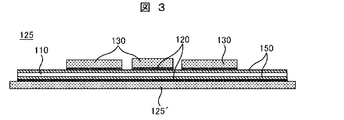
- FIG. 3 is a schematic cross-sectional view of a circuit board for a semiconductor device of the present invention.
- the circuit board 125 is one of the silicon nitride plates 110 (thermal expansion coefficient: 3.4 ppm / ° C., thermal conductivity: 90 W / m ⁇ K, thickness: 0.3 mm, size: 30 ⁇ 50 mm) 110 which is the ceramic substrate 110.
- the circuit wiring board 130 is bonded to the main surface of the ceramic substrate 110 by the silver-based bonding layer 120, and the support member 125 ′ made of copper or copper alloy is bonded to the other surface of the ceramic substrate 110 by the silver-based bonding layer 120.
- the bonding layer 120 is adjusted to a thickness of 50 ⁇ m
- the circuit wiring board 130 is adjusted to a thickness of 0.4 mm.
- An oxide film 150 having a thickness of 5 ⁇ m is formed on the surface of the ceramic substrate 110.
- the circuit wiring board 130 and the support member 125 ′ on the insulating substrate 125 are required to have (a) a high thermal conductivity, (b) excellent bondability with the ceramic board 110, and the like.
- (A) has an important meaning that the heat flow released from the semiconductor substrate is efficiently released to the outside when passing through the matrix region.
- a Ni plating layer (thickness: 6 ⁇ m, not shown) is formed on the surface metal layers of the circuit wiring board 130 and the support member 125 ′ in the electroless wet plating process.
- the reason for providing the Ni plating layer on the circuit wiring board 130 is to improve the wire bonding property of the circuit wiring board 130.
- a Ni plating layer is provided in the sense of blocking the outside air atmosphere to prevent internal alteration.
- the circuit board 125 is manufactured by first printing the above-mentioned silver oxide paste on a ceramic plate, then laminating metal plates (copper plates) for wiring and backing on both sides of the ceramic plate, and pressing the laminate. , Heat and join metal plate and ceramic plate. Ceramics are surface oxidized in a nitride system. The oxidation method was performed by heating in the atmosphere at 1000 ° C. for 60 minutes. As the silver oxide paste, a mixture of 90 wt% silver oxide particles containing 5 wt% myristyl alcohol and 10 wt% glycol solvent was used. This silver oxide paste is placed between the members to be joined, and in this state, heat at 400 ° C. is applied for about 60 minutes, and at the same time, a pressure of 1.0 MPa is applied in the atmosphere to perform joining. The sintered body after joining is pure silver. In addition, ultrasonic vibration can be applied during bonding.
- the circuit board 125 is reflected in simplification of the manufacturing process of the subsequent semiconductor device.
- the supporting member 125 ′ also serving as a heat sink and the ceramic substrate 110 serving also as an insulating plate are integrated by the bonding layer 120, and the circuit wiring board 130 is formed on the semiconductor substrate mounting surface of the ceramic substrate 110. ing. Therefore, at the stage of manufacturing the semiconductor device 1000, it is only necessary to mount the semiconductor substrate 101 which is another main member. This can reduce man-hours and the number of parts compared with the conventional method at the stage of assembling the semiconductor device 1000. This naturally contributes to the cost reduction of the semiconductor device 1000. Further, with the simplification of the vertical structure, it can greatly contribute to the reduction of the thermal resistance of the semiconductor device. In order to complete the semiconductor device, it is necessary to go through steps such as wire bonding, resin case attachment, and resin molding. These steps are common to the conventional steps.
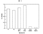
- FIG. 4 shows the result of the joint strength evaluation performed on the joint part of the present invention, and shows the result of investigating the influence of the joint partner material with the joint temperature set to 400 ° C. and the pressure of 1.0 MPa constant.
- the silver oxide paste used in this evaluation was composed of 90 wt% silver oxide particles (containing 5 wt% myristyl alcohol, pure silver after bonding) and 10 wt% glycol solvent (purified silver after bonding), the atmosphere In particular, bonding to Au, Ag, and Si 3 N 4 (with or without surface oxidation) and AlN (with or without surface oxidation) was performed.
- the vertical axis in FIG. 4 indicates the shear strength, which is normalized by the shear strength value with respect to the Ag electrode.
- the bonding strength to the surface-oxidized high thermal conductivity nitride ceramics is equal to or higher than the bonding strength to Au and Ag, and strong bonding is achieved.
- the bonding strength to nitride ceramics (Si 3 N 4 , AlN) that was not surface oxidized was significantly lower than that in the case of oxidation, and a strong bonding was not obtained.
- FIG. 5 shows the bonding strength to the surface-oxidized high thermal conductive nitride ceramics (Si 3 N 4 , AlN), and shows the shear strength with respect to the thickness of the surface oxide film layer.
- the vertical axis is normalized by the shear strength value for the Ag electrode, as in FIG.
- the oxide film thickness was 1 nm or more, the strength became high, and when it exceeded 10 ⁇ m, the strength decreased.
- the reason why the strength is lowered when the thickness is increased is that shear fracture occurs in the oxide film layer.
- high strength can be ensured even if the surface is slightly oxidized. This has the advantage of increasing the bonding strength without impairing the thermal conductivity.
- FIG. 6 and 7 are views showing a state of a cross section of the joint portion with the surface oxidized Si 3 N 4 of FIG.
- the sintered silver layer 120 formed on the surface of the nitride ceramic 110 is in a joined state via the oxide layer 150 as shown in FIG.
- the thickness of the oxide layer on the surface of the nitride ceramic is 1 nm to 10 ⁇ m, and the region having a thickness of 0.1 nm to 100 nm from the interface with the sintered silver is in an amorphous state.
- the oxide layer at the joint between the ceramic substrate and the sintered body is an amorphous layer 1501 as shown in FIG.
- the oxide layer on the surface of the ceramic substrate in the region not joined by the sintered body is composed only of the polycrystalline layer. That is, the oxide layer on the surface of the ceramic substrate before bonding is composed of a polycrystalline layer, but the amorphous layer and the sintered body are formed by replacing the polycrystalline layer at the bonding interface with the amorphous layer during bonding. It is presumed that strong bonding is achieved at the interface. Further, even when surface oxidized AlN was used, the bonding state was the same as that when the surface oxidized Si 3 N 4 was used.
- the polycrystalline oxide layer and the amorphous layer described above are oxide layers of elements constituting the ceramic substrate.
- the oxide polycrystalline layer and amorphous layer are composed of SiO 2
- the oxide polycrystalline layer and amorphous layer are It is composed of Al 2 O 3 .
- FIG. 8 shows the bonding strength with respect to the thickness of the amorphous layer.
- the vertical axis is normalized by the shear strength value for the Ag electrode, as in FIG. As a result, it was found that when the amorphous film thickness is 0.1 nm or more, the strength becomes high, and when it exceeds 100 nm, the strength decreases.
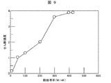
- FIG. 9 shows a change in shear strength of the surface silicon oxynitride plate with respect to the thermal conductivity of the sintered silver bonding layer.
- the vertical axis is normalized by the shear strength value for the Ag electrode, as in FIG. As a result, it was found that good bonding strength was exhibited at 50 W / mK or more. It has also been found that when it exceeds 400 W / mK, the strength is equivalent to the bulk value of 430 W / mK.
- the back metal plate 125 ′ and the wiring board 130 may be made of a copper-based material, aluminum, or an aluminum-based material other than copper.
- silver oxide particles were used as the metal particle precursor of the bonding material, but it has been confirmed that copper oxide can also be selected. Furthermore, silver acetate, silver formate, copper acetate, and copper formate can be selected, and it has been confirmed that the same effect is obtained.
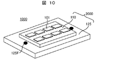
- FIG. 10 is a schematic diagram for explaining a main part of the semiconductor device.
- This figure shows a state in which a semiconductor substrate 101 is soldered and mounted on an insulating substrate 2000 in which a silicon nitride plate (30 ⁇ 50 ⁇ 0.3 mm; surface oxidation) as a ceramic plate 110 and a copper plate 125 as a support member are integrated.
- An Ni plating layer (thickness: 6 ⁇ m, not shown) is provided on the exposed portion of the support member 125.
- the support member 125 has a size of 42.4 mm ⁇ 85 mm ⁇ 3 mm, and a mounting hole (diameter: 5.6 mm) 125F is provided on the peripheral edge thereof.
- the support member 125 and the ceramic substrate 110 are integrated by a bonding layer 120 (thickness: 50 ⁇ m, not shown) made of a silver oxide-based material similar to that of the first embodiment, and the copper provided on the silicon nitride insulating plate 110.
- Eight MOS FET element bases (7 ⁇ 7 ⁇ 0.28 mm) 101 as semiconductor bases 101 are mounted on a circuit wiring board 130 (thickness: 0.4 mm, not shown) made of an alloy.
- the element base 101 and the circuit wiring board 130 are joined by an Sn-3Ag-0.5Cu solder material 113 (thickness: 100 ⁇ m, not shown).
- the semiconductor device 1000 of this example having such a main part structure has a maximum power consumption of 400 W, and the insulating substrate 2000 having the cross-sectional structure shown in FIG. 2 is applied.
Landscapes
- Chemical & Material Sciences (AREA)
- Engineering & Computer Science (AREA)
- Ceramic Engineering (AREA)
- Materials Engineering (AREA)
- Structural Engineering (AREA)
- Organic Chemistry (AREA)
- Manufacturing & Machinery (AREA)
- Inorganic Chemistry (AREA)
- Cooling Or The Like Of Semiconductors Or Solid State Devices (AREA)
Abstract
本発明は、製造時の熱応力ないし熱ひずみを軽減し、低熱抵抗,低コストの回路基板およびそれを用いた半導体装置を提供することを目的とし、窒化物を含むセラミックス基板と、前記セラミックス基板の一方の面に接合層を介して接合された回路配線板と、前記セラミックス基板の他方の面に接合層を介して接合された金属支持部材と、を備え、前記接合層が銀または銅を含む焼結体であり、前記セラミックス基板と前記焼結体の接合界面に酸化物層を有し、前記酸化物層は前記セラミックス基板側が多結晶層で構成され、前記焼結体側が非晶質層で構成される回路基板を特徴とする。
Description
本発明はパワー半導体モジュール等に適用するセラミックス回路基板、およびそれを用いた半導体装置に関する。
半導体素子基体を金属支持部材上に搭載した半導体装置は、全ての電極が金属支持部材を含む全てのパッケージ部材から電気的に絶縁して外部へ引き出されているため、回路適用上の自由度が高い。例えば、一対の主電極が回路上の接地電位から浮いている使用例であっても、電極電位とは無関係にパッケージを接地電位部に固定できるので半導体装置の実装が容易になる。
半導体素子を安全かつ安定に動作させるためには、半導体装置の動作時に発生する熱をパッケージの外へ効率良く放散させる必要がある。この熱放散は通常、発熱源である半導体素子基体からこれと接着された各部材を通じて気中へ熱伝達させることで達成される。半導体装置では、この熱伝達経路中に絶縁体,半導体基体を接着する部分等に用いられる接着材層,金属支持部材等が含まれる。
また、半導体装置を含む回路の扱う電力が高くなり、要求される信頼性(経時的安定性,耐湿性,耐熱性等)が高くなるほど、完全な絶縁性が要求される。ここで言う耐熱性には、半導体装置の周囲温度が外因により上昇した場合のほか、半導体装置の扱う電力が大きく、半導体基体で発生する熱が大きくなった場合の耐熱性も含む。
一方、半導体装置では一般に半導体素子基体を含むあるまとまった電気回路が組み込まれるため、その回路の少なくとも一部と支持部材とを電気的に絶縁する必要がある。例えば、第1先行技術として、Siチップを両面に銅板が接合されたAlNセラミックス基板(以下、銅貼りAlN基板と言う)に搭載したアッセンブリを、銅支持部材にはんだ付け一体化したパワーモジュール装置が知られている。
この第1先行技術において、銅貼りAlN基板はAlNの持つ高熱伝導性(190W/m・K),低熱膨張係数(4.3ppm/℃),高絶縁性(1015Ω・cm)等の特徴と、銅の持つ高熱伝導性(403W/m・K),高電気伝導性(1.7×10-6Ω・cm)等の特徴とを組み合わせたもので、電流密度が高く、発熱の著しい電力用半導体素子基体(Si:3.5ppm/℃)を直接はんだ付け搭載し、優れた放熱性と信頼性を備えたモジュール装置を得るのに有効な部品である。
一般に、銅貼りAlN基板は、これにはんだ付け搭載された半導体素子基体、又はこれに形成された電気回路を銅支持部材から電気的に絶縁するとともに、半導体基体から冷却フィンに至る熱流路を形成してその放熱効果を高める役割を担う。また、銅貼りAlN基板によれば、熱膨張係数の小さい半導体基体を特別な熱膨張緩和材(例えば、MoやW)を用いずに直接搭載できるため、パワーモジュール装置の部品点数や組み込み工数を削減できる。
又、第2先行技術(特許文献1)には、サイリスタチップをアルミナ基板に搭載したアッセンブリを、Al又はAl合金にSiCセラミックス粉末を分散させた複合材(以下、Al/SiC複合材と言う)からなる支持部材に搭載した半導体モジュール装置が開示されている。本先行技術において、アルミナ基板(7.5ppm/℃)はこれと熱膨張係数が略近似したAl/SiC複合材支持部材(6.7~14ppm/℃)に搭載されているため、これら部材間の接続部は優れた信頼性を有し、放熱性劣化の防止に有効に作用する。
第3先行技術(特許文献2)には、セラミックス基板の両面にAl-Si系ろう材を介して回路配線用Al板と熱拡散用Al板をそれぞれ接着した絶縁基板と、Al/SiC複合材により形成されたヒートシンクとを、Al合金を介して接合したヒートシンク付セラミック回路基板が開示されている。これによれば、両面に変形抵抗の小さいAl板が接合されているためセラミックス基板のクラック破壊が防止され、ヒートシンクは熱拡散用Al板にヒートシンク中のAl合金を介してあらかじめ接合されているのでパワーモジュールの製作工数を削減できる。
第4先行技術(特許文献3)には、セラミックス基板とSiC粉末で形成された多孔質プリフォームを隣接させ、前記プリフォームに溶融Alを含浸することによりAl/SiC複合材を作製すると同時にAl/SiC複合材とセラミックス基板を溶融Alにより一体化接合し、セラミックス基板の表面にAl回路部を形成した回路基板が開示されている。これにより、低コストの回路基板を得ることが可能である。
一般に、半導体装置では第1先行技術のように、半導体基体をはんだ付け搭載した銅貼りAlN基板を、同様のはんだ付けにより銅支持部材と一体化している。ここで、熱伝導率の高い銅板が支持部材として用いられる理由は、銅貼りAlN基板から伝達される熱流を広げて放熱効果を高めるためである。
この場合、銅支持部材と銅貼りAlN基板の間の熱膨張係数差が大きいことに起因して、はんだ層の破壊,熱流路の遮断という信頼性低下を生じやすい。具体的には以下の(1)~(3)の問題がある。
(1)熱応力,ひずみ
銅貼りAlN基板と銅支持部材の熱膨張係数が互いに異なるため、これらの一体化物には残留熱応力ないし熱ひずみが発生する。銅貼りAlN基板や銅支持部材は一体化の際に、はんだ材の融点以上に加熱した後室温まで冷却する熱処理工程を経る。この場合、各部材ははんだ材の凝固点で互いに固定されたまま各部材固有の熱膨張係数に従って収縮し、接着部に熱応力ないし熱ひずみが残留するとともに変形を生ずる。
銅貼りAlN基板と銅支持部材の熱膨張係数が互いに異なるため、これらの一体化物には残留熱応力ないし熱ひずみが発生する。銅貼りAlN基板や銅支持部材は一体化の際に、はんだ材の融点以上に加熱した後室温まで冷却する熱処理工程を経る。この場合、各部材ははんだ材の凝固点で互いに固定されたまま各部材固有の熱膨張係数に従って収縮し、接着部に熱応力ないし熱ひずみが残留するとともに変形を生ずる。
一般に、電力用の半導体基体はサイズが大きく、また、半導体装置では複数の半導体基体や他の素子も搭載されるので、絶縁基板やろう付け部の面積も大きくなる。このため、残留熱応力や熱ひずみが大きく、各部材の変形も促進されやすい。半導体装置に稼働時の熱ストレスが繰返し与えられ、これが上記残留熱応力ないし熱ひずみに重畳されると、はんだ層(特に後述する#2はんだ層)の疲労破壊による熱流路の遮断を生ずる。このような事柄は半導体装置の正常動作を阻害する。
(2)そりによる熱的係合や絶縁板の破損
銅貼りAlN基板と銅支持部材の熱膨張係数が互いに異なるため、これらの一体化物にはそりを発生する。半導体装置にそりを生ずると、これを冷却フィンに取り付ける際に熱伝導グリースの装填が均一になされない。この結果、銅支持部材と冷却フィン間の熱的係合が良好になされず、この経路の放熱性が損なわれ、半導体装置の正常動作を困難にする。
銅貼りAlN基板と銅支持部材の熱膨張係数が互いに異なるため、これらの一体化物にはそりを発生する。半導体装置にそりを生ずると、これを冷却フィンに取り付ける際に熱伝導グリースの装填が均一になされない。この結果、銅支持部材と冷却フィン間の熱的係合が良好になされず、この経路の放熱性が損なわれ、半導体装置の正常動作を困難にする。
(3)組み立て工数の問題及び鉛フリーはんだ化の困難性
半導体基体と銅貼りAlN基板をはんだ付けする工程(#1はんだ層の形成)と、同様のはんだ付けによる銅貼りAlN基板と銅支持部材との一体化工程(#2はんだ層の形成)が必要で、半導体装置の組み立て工数が多くなる。また、一般には#1はんだ層と#2はんだ層の形成工程では温度階層性(異なる融点を持つはんだ材)が必要になるが、既存の鉛フリーはんだ材の組み合わせでは十分な温度階層性を得ることは困難である。
半導体基体と銅貼りAlN基板をはんだ付けする工程(#1はんだ層の形成)と、同様のはんだ付けによる銅貼りAlN基板と銅支持部材との一体化工程(#2はんだ層の形成)が必要で、半導体装置の組み立て工数が多くなる。また、一般には#1はんだ層と#2はんだ層の形成工程では温度階層性(異なる融点を持つはんだ材)が必要になるが、既存の鉛フリーはんだ材の組み合わせでは十分な温度階層性を得ることは困難である。
第2先行技術における支持部材は複合材であって、SiCセラミックス粉末からなる多孔質プリフォームにAlを主成分とする溶融金属を含浸させることにより、Alマトリックス金属中にSiC粉末を分散させたのものである(以下Al/SiCと言う)。この部材の熱膨張係数はSiC粉末の添加量によって制御されるため、上記(1)や(2)の問題はクリヤすることが可能である。しかし、半導体装置の組み立てには#1及び#2はんだ層形成の両工程を通す必要があり上記(3)の問題が残る。また、アルミナ絶縁部材とAl/SiC支持部材は別々の工程で作製されるためコストの問題が残る。
第3先行技術に基づくヒートシンク付き回路基板を用いて得られる半導体装置は、絶縁基板と支持部材があらかじめ一体化されているため、後続の半導体装置の組み立て工程は簡素化される。しかし、このヒートシンク付き回路基板は、それぞれ別工程で作製されたAl張りAlN板とAl/SiCヒートシンクを積層し、これらを加圧しながら真空中で加熱する工程を経て得られる。このプロセスには多大のコストを要し、最終的には半導体装置の廉価化の障害になる。また、あらかじめ製作されたAl張りAlN板とAl/SiCヒートシンクの表面に形成された酸化物が接合後の界面に残留し、この界面の接続性及び信頼性を損ないやすい。
第4先行技術に基づくセラミックス回路基板はAl/SiCベース板とセラミックス絶縁板があらかじめ直接一体化されているため、後続のパワーモジュール組み立て工程は簡素化される。しかも、Al合金溶湯を所定の型に注入することにより、一体化と同一工程でAl/SiCの製作とセラミックス絶縁板への配線が施される。このため、セラミックス回路基板を比較的低コストで製作できる可能性を持ち、最終的には半導体装置の廉価化に貢献できることが期待される。しかし、本構造の場合はAl/SiCベース板とセラミックス絶縁板が600℃を超える比較的高温のもとで直接一体化されるため、一体化物に応力やひずみ,そり変形を生じやすく、上述の(2)の問題が残る。
本発明の目的は、製造時の熱応力ないし熱ひずみを軽減し、低熱抵抗,低コストの回路基板およびそれを用いた半導体装置を提供することにある。
本発明の回路基板は、窒化物を含むセラミックス基板と、前記セラミックス基板の一方の面に接合層を介して接合された回路配線板と、前記セラミックス基板の他方の面に接合層を介して接合された金属支持部材と、を備え、前記接合層が銀または銅を含む焼結体であり、前記セラミックス基板と前記焼結体の接合界面に酸化物層を有し、前記酸化物層は前記セラミックス基板側が多結晶層で構成され、前記焼結体側が非晶質層で構成されていることを特徴とする。
また、前記酸化物層の厚さが1nm~10μmであり、前記非晶質層の厚さが0.1nm~100nmであることが好ましい。
また、前記セラミックス基板としては、窒化珪素または窒化アルミニウムを用いることが好ましい。この場合、前記酸化物層は珪素またはアルミニウムの酸化物である。
また、前記焼結体の熱伝導率が50W/mK~430W/mKであることが好ましい。
また、本発明の半導体装置は、上記回路基板の回路配線板上に半導体素子を搭載することにより得られる。
以上説明したように本発明は、製造時に生ずる熱応力ないし熱ひずみを軽減し、放熱性が優れるとともに、低コストの回路基板および半導体装置を提供することができる。また、接合部の少数化の実現により、長期信頼性の確保が容易になり、かつ製造プロセスの簡略化も実現できる。これらのことから大幅なコストダウンを図ることができる。
以下、本発明の実施形態を説明する。
図1は、本発明に係る回路基板の構成を説明する図である。回路基板125は、窒化物を含むセラミックス基板110と、セラミックス基板110の一方の面に接合層120を介して接合された回路配線板130と、セラミックス基板110の他方の面に接合層120を介して接合された支持部材125′で構成される。後述するようにセラミックス基板110と接合層120の接合界面には酸化物層を有し、酸化物層はセラミックス基板側が多結晶層となり、焼結体側が非晶質層となっている。
支持部材125′は、耐熱性,熱伝導性に優れた金属または金属を含む複合材料が適している。具体的には、銅または銅を含む合金、またはアルミニウムまたはアルミニウムを含む合金が良い。
また、支持部材125′と接合層120が接する面とは相対する面に、凹凸状のフィンを設けて放熱性を向上させても良い。
セラミックス基板110は、耐熱性,耐圧性に優れ、高強度なセラミックスが適している。セラミックス材料として、アルミニウムや珪素を含む酸化物や窒化物が挙げられるが、中でも高強度かつ熱伝導性の良い窒化物が好ましい。具体的には窒化アルミニウム,窒化珪素が挙げられる。特に、窒化珪素は高強度セラミックスとして知られている。また、絶縁基板の厚さは回路基板110に求められる絶縁耐圧および強度で決められる。セラミックス板は必要に応じて複数枚搭載されていてもよく、この際窒化珪素板,窒化アルミニウム板を必要に応じて組み合わせてもよい。
回路配線板130は、耐熱性,熱伝導性、そして導電性に優れた金属または金属を含む複合材料が適している。具体的には、銅または銅を含む合金、またはアルミニウムまたはアルミニウムを含む合金が良い。
接合層120には、銀または銅を含む焼結体を用いる。接合層120は、支持部材125′とセラミックス基板110、およびセラミックス基板110と回路配線板130のそれぞれの界面を低温で接合できることが望ましい。低温で接合することにより、接合部に残留する熱応力および反りを低減できるためである。
金属焼結体により低温で接合する接合技術としては、金属ナノ粒子の低温焼成機能を利用した接合材料が知られている。しかしながら、従来の平均粒径100nm以下の金属粒子を接合の主剤とする接合材料を用いた場合では、金属とセラミックスは接合できない。一方、金属酸化物粒子と金属酸化物粒子を還元する有機物からなる還元剤から構成される接合材を用いた接合技術がある。この接合技術は、接合時における加熱と加圧時に金属酸化物粒子が還元されることで平均粒径100nm以下の金属粒子が生成され、平均粒径100nm以下の金属粒子の焼結が起こり、バルクな金属に変化するという現象を利用したものである。この接合技術によれば、酸化物系のセラミックスであるアルミナに対しても接合が可能である。しかしながら、窒化物系のセラミックスに対しては十分な接合強度を得ることはできない。これは、非酸化物系セラミックスの絶縁基板との接合では、酸化金属粒子の還元反応熱で金属元素をセラミックス内部に拡散させて接合強度を強める必要があるが、窒化物中に金属元素を拡散させるのが容易でないためである。そこで、本発明者らが誠意検討した結果、窒化物系セラミックス表面に金属元素が拡散しやすい酸化層を形成し、金属粒子の拡散を促進することで、窒化物系のセラミックスに対して接合ができることを見出した。すなわち、窒化物系のセラミックスの表面に酸化物層を形成して、金属粒子前駆体である平均粒径が1nm~100μmの金属酸化物粒子と金属酸化物粒子を還元する有機物からなる還元剤から構成される接合材を用いて大気雰囲気中において接合を行うことにより、窒化物セラミックスに対して優れた接合強度を得ることができる。接合後のセラミックス基板と前記焼結体の接合界面には酸化物層が存在しており、この酸化物層はセラミックス基板側が多結晶層で構成され、焼結体側が非晶質層で構成されている。この酸化物層の厚さを1nm~10μmとし、非晶質層の厚さを0.1nm~100nmとすることで優れた接合強度を得ることができる。
セラミックス基板に酸化物層を形成する方法としては、例えば、セラミックス基板を大気中で1000℃の温度で焼成することで、厚さ数nmの酸化層をセラミックス表面に形成できる。また、高濃度の酸素雰囲気中で焼成しても良い。また、蒸着法,溶射法,エアロゾルデポジション法による成膜技術を利用して絶縁基板表面に酸化層を形成することも可能である。
本接合では、金属粒子前駆体に対して有機物からなる還元剤を添加することによって、金属粒子前駆体単体を加熱分解するよりも低温で金属粒子前駆体が還元され、その際に平均粒径が100nm以下の金属粒子が作製され、金属粒子同士が相互に融合することで接合が行われるという現象を利用している。酸化銀粒子は還元剤の存在下では、200℃以下で100nm以下の金属粒子が作製され始めることから、従来困難であった500℃以下の低温でもセラミックスと金属との接合を達成することが可能である。また、接合中においてその場で粒径が100nm以下の金属粒子が作製されるため、有機物で表面を保護した金属粒子の作製が不要であり、接合用材料の製造,接合プロセスの簡易化,接合材料の大幅なコストダウンを達成することが可能である。また還元剤の還元発熱作用により窒化物セラミックス表面に形成した酸化物層表面が活性状態になり、この表面活性化した酸化物層と銀が強固な結合を達成することができる。
窒化物を含むセラミックス基板と回路配線板,支持部材を接合する接合材料について説明する。上述のように、本発明で使用する接合材料は、金属粒子前駆体である平均粒径が1nm~100μmの金属酸化物粒子と金属酸化物粒子を還元する有機物からなる還元剤から構成される接合材料である。
100nm以下の金属粒子を作製する平均粒径が1nm以上100μm以下の金属粒子前駆体として、金属酸化物と規定したのは金属粒子前駆体中における金属含有量が高いことから、接合時における体積収縮が小さく、かつ分解時に酸素を発生するために、有機物の酸化分解を促進するからである。上記接合材に用いられる金属酸化物粒子としては、酸化銀(Ag2O,AgO)のほか、酸化銅(CuO)も挙げられ、これらの群から少なくとも1種類以上の金属を用いることができる。酸化銀(Ag2O,AgO),酸化銅(CuO)からなる金属酸化物粒子は還元時に酸素のみを発生するために、接合後における残渣も残りにくく、体積減少率も小さい。また、金属酸化物粒子は、平均粒径が1nm以上100μm以下、好ましくは50μm以下の粒子とすることが望ましい。平均粒径を100μm以下としたのは、金属酸化物粒子の還元によって接合中に粒径が100nm以下の金属粒子が生成されにくくなり、これにより粒子間の隙間が多くなり、緻密な接合層を得ることが困難になるためである。また、平均粒径を1nm以上としたのは、平均粒径が1nm以下の金属酸化物粒子を作製することが困難なためである。また、この接合材では、接合中に100nm以下の金属粒子が生成されることで接合が行われるため、金属酸化物粒子の粒径は100nm以下とする必要はなく、金属酸化物粒子の作製,取扱い性,長期保存性の観点からは平均粒径が1μm以上の粒子を用いることが好ましい。また、より緻密な接合層を得るために粒径が1nm~100nmの金属粒子前駆体を用いることも可能である。
金属粒子前駆体の含有量としては、接合材料中における全質量部において50質量部を超えて99質量部以下とすることが好ましい。これは接合材料中にける金属含有量が多い方が低温での接合後に有機物残渣が少なくなり、低温での緻密な焼成層の達成及び接合界面での金属結合の達成が可能となり、接合強度の向上さらには高放熱性,高耐熱性を有する接合層とすることが可能になるからである。
上記接合材に用いられる還元剤としては、金属酸化物粒子を還元する作用を有するものであればよく、例えば、アルコール類,カルボン酸類,アミン類から選ばれた1種類以上の有機物を用いることができる。また、用いる還元剤は上記アルコール,カルボン酸,アミンを含む有機物に限らず、アルデヒド基やエステル基,スルファニル基,ケトン基などを含む有機物を用いても良い。
利用可能なアルコール基を含む化合物としては、アルキルアルコールが挙げられ、例えば、エタノール,プロパノール,ブチルアルコール,ペンチルアルコール,ヘキシルアルコール,ヘプチルアルコール,オクチルアルコール,ノニルアルコール,デシルアルコール,ウンデシルアルコール,ドデシルアルコール,トリデシルアルコール,テトラデルアルコール,ペンタデシルアルコール,ヘキサデシルアルコール,ヘプタデシルアルコール,オクタデシルアルコール,ノナデシルアルコール,イコシルアルコール、がある。さらには1級アルコール型に限らず、2級アルコール型,3級アルコール型、及びアルカンジオール,環状型の構造を有するアルコール化合物を用いることが可能である。それ以外にも、エチレングリコール,トリエチレングリコールなど多数のアルコール基を有する化合物を用いてもよく、また、クエン酸,アスコルビン酸,グルコースなどの化合物を用いてもよい。
また、利用可能なカルボン酸を含む化合物としてアルキルカルボン酸がある。具体例としては、ブタン酸,ペンタン酸,ヘキサン酸,ヘプタン酸,オクタン酸,ノナン酸,デカン酸,ウンデカン酸,ドデカン酸,トリデカン酸,テトラデカン酸,ペンタデカン酸,ヘキサデカン酸,ヘプタデカン酸,オクタデカン酸,ノナデカン酸,イコサン酸が挙げられる。また、上記アミノ基と同様に1級カルボン酸型に限らず、2級カルボン酸型,3級カルボン酸型、及びジカルボン酸,環状型の構造を有するカルボキシル化合物を用いることが可能である。
また、利用可能なアミノ基を含む化合物としてアルキルアミンを挙げることができる。例えば、ブチルアミン,ペンチルアミン,ヘキシルアミン,ヘプチルアミン,オクチルアミン,ノニルアミン,デシルアミン,ウンデシルアミン,ドデシルアミン,トリデシルアミン,テトラデシルアミン,ペンタデシルアミン,ヘキサデシルアミン,ヘプタデシルアミン,オクタデシルアミン,ノナデシルアミン,イコデシルアミンがある。また、アミノ基を有する化合物としては分岐構造を有していてもよく、そのような例としては、2-エチルヘキシルアミン、1,5ジメチルヘキシルアミンなどがある。また、1級アミン型に限らず、2級アミン型,3級アミン型を用いることも可能である。さらにこのような有機物としては環状の形状を有していてもよい。
また、還元剤にはカルボン酸金属塩を用いても良い。接合温度よりも低い融点を有する還元剤は接合時に凝集し、ボイドの原因となるが、カルボン酸金属塩は接合時の加熱により融解しないため、ボイド低減のために用いることが可能である。カルボン酸金属塩以外にも有機物を含有する金属化合物であれば還元剤として用いても良い。
ここで、エチレングリコール,トリエチレングリコール等の20~30℃において液体である還元剤は、酸化銀(Ag2O)などと混ぜて放置すると一日後には銀に還元されてしまうため、混合後はすぐに用いる必要がある。一方、20~30℃の温度範囲において固体であるミリスチルアルコール,ラウリルアミン,アスコルビン酸等は金属酸化物等と1ヵ月ほど放置しておいても大きくは反応が進まないため、保存性に優れており、混合後に長期間保管する場合にはこれらを用いることが好ましい。また、用いる還元剤は金属酸化物等を還元させた後には、精製された100nm以下の粒径を有する金属粒子の保護膜として働くために、ある程度の炭素数があることが望ましい。具体的には、2以上で20以下であることが望ましい。これは炭素数が2より少ないと、金属粒子が作製されると同時に粒径成長が起こり、100nm以下の金属粒子の作製が困難になるからである。また、20より多いと、分解温度が高くなり、金属粒子の焼結が起こりにくくなった結果、接合強度の低下を招くからである。
還元剤の使用量は金属粒子前駆体の全重量に対して1質量部以上で50質量部以下の範囲であればよい。これは還元剤の量が1質量部より少ないと接合材料における金属粒子前駆体を全て還元して金属粒子を作製するのに十分な量ではないためである。また、50質量部を超えて用いると接合後における残渣が多くなり界面での金属接合と接合銀層中における緻密化の達成が困難であるためである。さらに、還元剤が有機物のみから構成される場合には、400℃までの加熱時における熱重量減少率が99%以上であることが好ましい。これは、還元剤の分解温度が高いと接合後における残渣が多くなり、界面での金属接合と接合銀層中における緻密化の達成が困難であるためである。ここで、400℃までの加熱時における熱重量減少率の測定は、一般に市販されている、Seiko Instruments製TG/DTA6200や、島津製作所製TGA-50等の熱重量測定が可能な装置を用いて10℃/minにおいて大気中で行った場合のものとする。
金属粒子前駆体と有機物からなる還元剤の組み合わせとしては、これらを混合することにより金属粒子を作製可能なものであれば特に限定されないが、接合用材料としての保存性の観点から、常温で金属粒子を作製しない組み合わせとすることが好ましい。
また、接合材料中には比較的粒径の大きい平均粒径50μm~100μmの金属粒子を混合して用いることも可能である。これは接合中において作製された100nm以下の金属粒子が、平均粒径50μm~100μmの金属粒子同士を焼結させる役割を果たすからである。また、粒径が100nm以下の金属粒子を予め混合しておいてもよい。この金属粒子の種類としては、金,銀,銅があげられる。上記以外にも白金,パラジウム,ロジウム,オスミウム,ルテニウム,イリジウム,鉄,錫,亜鉛,コバルト,ニッケル,クロム,チタン,タンタル,タングステン,インジウム,ケイ素,アルミニウム等の中から少なくとも1種類の金属あるいは2種類以上の金属からなる合金を用いることが可能である。
この実施形態で用いられる接合材料は金属粒子前駆体と有機物からなる還元剤のみで用いてもよいが、ペースト状として用いる場合に溶媒を加えてもよい。混合後、すぐに用いるのであれば、メタノール,エタノール,プロパノール,エチレングリコール,トリエチレングリコール,テルピネオールのアルコール類等の還元作用があるものを用いてもよいが、長期間に保管する場合であれば、水,ヘキサン,テトラヒドロフラン,トルエン,シクロヘキサン、など常温での還元作用が弱いものを用いることが好ましい。また、還元剤としてミリスチルアルコールのように常温で還元が起こりにくいものを用いた場合には長期間保管可能であるが、エチレングリコールのような還元作用の強いものを用いた場合には使用時に混合して用いることが好ましい。
また、金属粒子前駆体の溶媒への分散性を向上させるために必要に応じて分散剤を用いて金属粒子前駆体の周りを有機物で被覆し、分散性を向上させてよい。本発明で用いられる分散剤としては、ポリビニルアルコール,ポリアクリルニトリル,ポリビニルピロリドン,リエチレングリコールなどの他に、市販の分散剤として、例えばディスパービック160,ディスパービック161,ディスパービック162,ディスパービック163,ディスパービック166,ディスパービック170,ディスパービック180,ディスパービック182,ディスパービック184,ディスパービック190(以上ビックケミー社製),メガファックF-479(大日本インキ製),ソルスパース20000,ソルスパース24000,ソルスパース26000,ソルスパース27000,ソルスパース28000(以上、アビシア社製)などの高分子系分散剤を用いることができる。このような分散剤の使用量は金属粒子前駆体に接合用材料中において0.01wt%以上でかつ45wt%を超えない範囲とする。
これらペースト材料は、インクジェット法により微細なノズルからペーストを噴出させて基板上の電極あるいは電子部品の接続部に塗布する方法や、あるいは塗布部分を開口したメタルマスクやメッシュ状マスクを用いて必要部分にのみ塗布を行う方法,ディスペンサを用いて必要部分に塗布する方法,シリコーンやフッ素等を含む撥水性の樹脂を必要な部分のみ開口したメタルマスクやメッシュ状マスクで塗布したり、感光性のある撥水性樹脂を基板あるいは電子部品上に塗布し、露光および現像することにより前記微細粒子等からなるペーストを塗布する部分を除去し、その後接合用ペーストをその開口部に塗布する方法や、さらには撥水性樹脂を基板あるいは電子部品に塗布後、前記金属粒子からなるペースト塗布部分をレーザーにより除去し、その後接合用ペーストをその開口部に塗布する方法がある。これらの塗布方法は、接合する電極の面積,形状に応じて組み合わせ可能である。また、ミリスチルアルコールやアスコルビン酸のような常温で固体のものを還元剤として用いた際には金属粒子前駆体と混合し加圧を加えることでシート状に成形して接合材料として用いる方法がある。
本接合材料を用いた接合では、接合時に金属粒子前駆体から粒径が100nm以下の金属粒子を作製し、接合層における有機物を排出しながら粒径が100nm以下の金属粒子の融着による金属結合を行うために熱と圧力を加えることが必須である。接合条件としては、1秒以上10分以内で50℃以上400℃以下の加熱と0.01~10MPaの加圧を加えることが好ましい。
本発明の接合では、金属酸化物粒子は接合時の加熱によって粒径0.1~50nm程度の酸化物ではない純金属超微粒子化し、この純金属超粒子同士が相互に融合してバルクになる。バルクになった後の溶融温度は通常のバルクの状態での金属の溶融温度と同じであり、純金属超微粒子は低温の加熱で溶融し、溶融後はバルクの状態での溶融温度に加熱されるまで再溶融しないという特徴を有する。これは、純金属超微粒子を用いた場合に低い温度で接合を行うことができ、接合後は溶融温度が向上することから、その後、他の電子部品を接合している際に接合部が再溶融しないというメリットをもたらす。また、接合後の接合層の熱伝導率は50乃至430W/mKとすることが可能であり、放熱性にも優れている。さらに前駆体が金属酸化物であるため低コストというメリットもある。なお、金属酸化物粒子には還元効果を促進するため、アルコールなどの有機物を被膜させておくことが必要である。接合時の雰囲気は大気雰囲気でよい。
以上の接合材料と接合方法を経て接合された界面には非晶質層が形成される。還元して生成した金属粒子は、接合によって相手部材と金属的に結合されることが接合強度を高めるために要求される。なお、酸化銀と酸化銅混在の場合も上述と同様に接合でき、かつ耐食性向上が図れる利点を有する。
図1で示した回路基板の回路配線板130に半導体素子を接合することによって半導体装置を得ることができる。
以上で説明した接合材,接合方法をセラミックス基板と回路配線板、支持部材との間の接合に用いることにより、製造時の熱応力ないし熱ひずみを軽減し、低熱抵抗,低コストの回路基板およびそれを用いた半導体装置を得ることが可能となる。
以下、図面を用いて、本発明の実施例を説明するが、本発明は、以下の実施形態に限定されるものではない。
〔実施例〕
(実施例1)
図2は本発明の半導体装置1000の基本構造を説明する平面及び断面模式図である。(a)は平面図、(b)は(a)におけるA-A′断面をそれぞれ示す。セラミックス基板110として表面に酸化物層150が形成された窒化珪素を用いた。セラミックス基板110の一方の面に銅製の回路配線板130が銀系の接合層120で接合され、他方の面に銅製の支持部材125′が銀系の接合層120で接合されて回路基板125を構成している。回路配線板130の上には半導体基体101が搭載されている。半導体基体101はMOS FET素子である。主端子30や補助端子31を設けてあるポリフェニルサルファイド製の樹脂ケース20が支持部材125′に取り付けられている。素子基体101と回路配線板130の間、半導体素子基体101と補助端子31の間、回路配線板130と主端子30の間には、Al細線117のワイヤボンディングが施されている。樹脂ケース20内にはシリコーンゲル樹脂22が充填され、樹脂ケース20の上部にはポリフェニルサルファイド製の樹脂蓋21が設けられている。ここで、セラミックス基板110に設けられた回路配線板130上には8個の素子基体101が銀系の接合層113により固着されている。また、回路配線板130には温度検出用サーミスタ素子がはんだ(いずれも図示を省略)により接合され、回路配線板130はAl細線117により補助端子31へ連絡されている。なお、図面では省略しているが、樹脂ケース20と支持部材125′の間、そして樹脂ケース20と樹脂蓋21の間はシリコーン接着樹脂(図示を省略)を用いて固定されている。樹脂蓋21の肉厚部には凹み25,主端子30には穴30′がそれぞれ設けられ、半導体装置1000を外部回路配線に連絡するためのネジ(図示を省略)が収納されている。主端子30や補助端子31はあらかじめ所定形状に打抜き成形された銅板にNiめっきを施したものであり、射出成形法によって樹脂ケース20に取り付けられている。
図3は、本発明の半導体装置用回路基板の断面模式図である。回路基板125は、セラミックス基板110である窒化珪素板(熱膨張係数:3.4ppm/℃,熱伝導率:90W/m・K,厚さ:0.3mm,サイズ:30×50mm)110の一方の主面に回路配線板130が銀系の接合層120により接合され、セラミックス基板110の他方の面に銅または銅合金からなる支持部材125′が銀系の接合層120により接合された構成を備える。ここで、接合層120は厚さ50μm、回路配線板130は厚さ0.4mmに調整されている。セラミックス基板110の表面には厚さ5μmの酸化物膜150が形成されている。
絶縁基板125における回路配線板130と支持部材125′は、(a)熱伝導率の高い点、(b)セラミックス板110との接合性に優れること等が要求される。(a)は半導体基体から放出された熱流がマトリックス領域を経由する際に効率良く外部へ放出されるのに重要な意味を持つ。
上述の配線,放熱板一体化基板は、無電解湿式めっき工程にて回路配線板130と支持部材125′の表面金属層にNiめっき層(厚さ:6μm 図示せず)が形成される。回路配線板130にNiめっき層を設ける理由は、回路配線板130のワイヤボンディング性を高める点にある。また、外気雰囲気から遮断して内部の変質を防ぐ意味でNiめっき層が設けられる。
回路基板125の製造工程は、先ずセラミックス板には前述した酸化銀系のペーストを印刷した後、セラミックス板の両面に配線用及び裏打ち用の金属板(銅板)を積層し、積層体を加圧,加熱して金属板とセラミックス板を接合する。セラミックスは窒化物系で表面酸化されている。酸化方法は、1000℃で大気中60分加熱により行った。酸化銀系ペーストはミリスチルアルコールを5wt%含有した90wt%の酸化銀粒子と、10wt%のグリコール系溶剤を混合したものを用いた。この酸化銀ペーストを接合すべき部材の間に配置し、その状態で400℃の熱を約60分間加え、同時に1.0MPaの圧力を大気中で加えることにより、接合を行うことができる。接合後の焼結体は純銀化されている。また、接合の際に超音波振動を加えることもできる。
回路基板125は、後続の半導体装置の製作工程の簡略化へ反映される。回路基板125においては既に、放熱板を兼ねる支持部材125′と絶縁板を兼ねるセラミックス基板110が接合層120により一体化され、しかもセラミックス基板110の半導体基体搭載面には回路配線板130が形成されている。したがって、半導体装置1000を製作する段階では、もう1つの主要部材である半導体基体101を搭載するだけでよい。このことは半導体装置1000の組み立て段階で従来法より工数と部品点数を削減できる。これは当然ながら半導体装置1000のコスト低減に寄与する。さらに縦構造の簡略化に伴い、半導体装置の低熱抵抗化に大きく寄与できる。なお、半導体装置を完成させるためにはワイヤボンディング,樹脂ケース取り付け,樹脂モールド等の工程を経る必要がある。これらの工程は従来工程の場合にも共通する点である。
図4は本発明の接合部位に対して行った接合強度評価結果を示したもので、接合温度を400℃、加圧1.0MPa一定とし、接合相手材との影響を調べた結果を示す。本評価で用いた酸化銀系ペーストは90wt%の酸化銀粒子(ミリスチルアルコールを5wt%含有、接合後は純銀化)と10wt%のグリコール系溶剤(接合後は純銀化)を混合した構成、大気中でそれぞれAu,Ag、及びSi3N4(表面酸化有無),AlN(表面酸化有無)への接合を行った。図4の縦軸はせん断強度を示し、Ag電極に対するせん断強度値で規格化したものである。
その結果、表面酸化した高熱伝導窒化物セラミックス(Si3N4,AlN)に対する接合強度は、Au,Agに対して接合した場合と同等以上の接合強度が得られており、強固な接合が達成されている。一方、表面酸化していない窒化物セラミックス(Si3N4,AlN)に対する接合強度は、酸化した場合に比べて大幅に低く、強固な接合は得られていないことが判った。
図5は表面酸化した高熱伝導窒化物セラミックス(Si3N4,AlN)に対する接合強度を示したもので、その表面酸化膜層の厚さに対するせん断強度を示したものである。縦軸は図4と同様、Ag電極に対するせん断強度値で規格化したものである。この結果、酸化膜厚さは1nm以上あると高強度になり、10μmを超えると強度は低下することが判った。厚くなると低強度になる理由は、せん断破壊が酸化膜層内で生じることによる。一方、わずかでも表面が酸化していれば高強度を確保できる。このことは、熱伝導率を損なわずに高接合強度化になる利点がある。
図6および図7は図3の表面酸化Si3N4との接合部断面の状態を示した図である。本実施例の回路基板では窒化物セラミックス110の表面に形成した焼結銀層120に対し、図6に示すような酸化物層150を介した接合状態にあり、特にその構造は、図7に示すように窒化物セラミックス表面の酸化物層の厚さが1nm乃至10μmで、かつ焼結銀との接合部界面から0.1nm乃至100nmの厚さの領域が非晶質状態である。なお、本実施例のようにセラミックス基板110の表面全体に酸化物を形成した場合には、セラミックス基板と焼結体の接合部における酸化物層は図7に示したように非晶質層1501と多結晶層1502で構成されているが、焼結体により接合されていない領域のセラミックス基板表面の酸化物層は多結晶層のみで構成されている。すなわち、接合前のセラミックス基板表面の酸化物層は多結晶層で構成されているが、接合時に接合界面の多結晶層が非晶質層にかわることで、非晶質層と焼結体との界面で強固な接合が達成されているものと推測される。また、表面酸化AlNを用いた場合であっても、上述した表面酸化Si3N4を用いた場合と同様の接合状態であった。なお、上述した酸化物の多結晶層及び非晶質層は、セラミックス基板を構成する元素の酸化物層となっている。例えば表面酸化Si3N4を用いた場合、酸化物の多結晶層及び非晶質層はSiO2から構成され、表面酸化AlNを用いた場合、酸化物の多結晶層及び非晶質層はAl2O3から構成される。
図8は、この非晶質層の厚さに対する接合強度を示したものである。縦軸は図4と同様、Ag電極に対するせん断強度値で規格化したものである。この結果、非晶質膜厚さは0.1nm以上あると高強度になり、100nmを超えると強度は低下することが判った。
図9は、焼結銀接合層の熱伝導率に対する表面酸化窒化珪素板に対するせん断強度変化を示したものである。縦軸は図4と同様、Ag電極に対するせん断強度値で規格化したものである。この結果、50W/mK以上で良好な接合強度を示すことが判った。400W/mKを超えるとバルク値430W/mKと同等の強度になることも判った。
なお、裏面金属板125′、配線板130は銅以外に、銅系材,アルミニウム,アルミニウム系材でもよい。
本実施例では、接合材の金属粒子前駆体として酸化銀粒子を用いたが、それ以外にも酸化銅も選択できることを確認している。さらに酢酸銀,ギ酸銀,酢酸銅,ギ酸銅も選択でき、同様の効果があることを確認している。
以上の結果より、酸化物金属粒子と還元剤を含む接合材料を用いて、大気中にて接合を行うことで表面酸化セラミックスへの接合が可能であることが判った。
(実施例2)
図10は半導体装置の要部を説明する模式図である。この図は、セラミックス板110としての窒化珪素板(30×50×0.3mm;表面酸化)と支持部材としての銅板125を一体化した絶縁基板2000に、半導体基体101をはんだ付け搭載した状態を示す。支持部材125の露出部にはNiめっき層(厚さ:6μm、図示を省略)が設けられている。支持部材125は42.4mm×85mm×3mmなる寸法を有し、その周縁部に取り付け穴(直径:5.6mm)125Fが設けられている。支持部材125とセラミックス基板110は実施例1と同様の酸化銀系系材からなる接合層120(厚さ:50μm、図示を省略)により一体化され、窒化珪素絶縁板110上に設けられた銅合金からなる回路配線板130(厚さ:0.4mm、図示を省略)に半導体基体101としてのMOS FET素子基体(7×7×0.28mm)101が8個搭載されている。
図10は半導体装置の要部を説明する模式図である。この図は、セラミックス板110としての窒化珪素板(30×50×0.3mm;表面酸化)と支持部材としての銅板125を一体化した絶縁基板2000に、半導体基体101をはんだ付け搭載した状態を示す。支持部材125の露出部にはNiめっき層(厚さ:6μm、図示を省略)が設けられている。支持部材125は42.4mm×85mm×3mmなる寸法を有し、その周縁部に取り付け穴(直径:5.6mm)125Fが設けられている。支持部材125とセラミックス基板110は実施例1と同様の酸化銀系系材からなる接合層120(厚さ:50μm、図示を省略)により一体化され、窒化珪素絶縁板110上に設けられた銅合金からなる回路配線板130(厚さ:0.4mm、図示を省略)に半導体基体101としてのMOS FET素子基体(7×7×0.28mm)101が8個搭載されている。
素子基体101と回路配線板130の間はSn-3Ag-0.5Cuはんだ材113(厚さ:100μm、図示を省略)により接合されている。このような要部構造を有する本実施例半導体装置1000は最大消費電力400Wのもので、図2に示した断面構造を有する絶縁基板2000が適用されている。
20 樹脂ケース
21 樹脂蓋
22 シリコーンゲル樹脂,エポキシ樹脂
25 凹み
30 主端子,端子
101 半導体基体,MOS FET素子基体,IGBT素子基体
110 セラミックス基板,窒化珪素板,窒化アルミニウム板
113,124 接合層
120 接合層
125 回路基板
125′ 支持部材
125F 取り付け穴
130 回路配線板
1000 半導体装置
21 樹脂蓋
22 シリコーンゲル樹脂,エポキシ樹脂
25 凹み
30 主端子,端子
101 半導体基体,MOS FET素子基体,IGBT素子基体
110 セラミックス基板,窒化珪素板,窒化アルミニウム板
113,124 接合層
120 接合層
125 回路基板
125′ 支持部材
125F 取り付け穴
130 回路配線板
1000 半導体装置
Claims (12)
- 窒化物を含むセラミックス基板と、
前記セラミックス基板の一方の面に接合層を介して接合された回路配線板と、
前記セラミックス基板の他方の面に接合層を介して接合された金属支持部材と、を備え、
前記接合層が銀または銅を含む焼結体であり、
前記セラミックス基板と前記焼結体の接合界面に酸化物層を有し、前記酸化物層は前記セラミックス基板側が多結晶層で構成され、前記焼結体側が非晶質層で構成されていることを特徴とする回路基板。 - 請求項1に記載の回路基板において、前記酸化物層の厚さが1nm~10μmであることを特徴とする回路基板。
- 請求項1または2に記載の回路基板において、前記非晶質層の厚さが0.1nm~100nmであることを特徴とする回路基板。
- 請求項1~3のいずれか1項に記載の回路基板において、前記セラミックス基板が窒化珪素または窒化アルミニウムであることを特徴とする回路基板。
- 請求項4に記載の回路基板において、前記酸化物層が珪素またはアルミニウムの酸化物であることを特徴とする回路基板。
- 請求項1~5のいずれか1項に記載の回路基板において、前記焼結体の熱伝導率が50W/mK~430W/mKであることを特徴とする回路基板。
- 窒化物を含むセラミックス基板と、
前記セラミックス基板の一方の面に接合層を介して接合された回路配線板と、
前記セラミックス基板の他方の面に接合層を介して接合された金属支持部材と、
前記回路配線板に搭載された半導体素子と、を備え、
前記接合層が銀または銅を含む焼結体であり、
前記セラミックス基板と前記焼結体の接合界面に酸化物層を有し、前記酸化物層は前記セラミックス基板側が多結晶層で構成され、前記焼結体側が非晶質層で構成されていることを特徴とする半導体装置。 - 請求項7に記載の半導体装置において、前記酸化物層の厚さが1nm~10μmであることを特徴とする半導体装置。
- 請求項7または8に記載の半導体装置において、前記非晶質層の厚さが0.1nm~100nmであることを特徴とする半導体装置。
- 請求項7~9のいずれか1項に記載の半導体装置において、前記セラミックス基板が窒化珪素または窒化アルミニウムであることを特徴とする半導体装置。
- 請求項10に記載の半導体装置において、前記酸化物層が珪素またはアルミニウムの酸化物であることを特徴とする半導体装置。
- 請求項7~11のいずれか1項に記載の半導体装置において、前記焼結体の熱伝導率が50W/mK~430W/mKであることを特徴とする半導体装置。
Priority Applications (2)
| Application Number | Priority Date | Filing Date | Title |
|---|---|---|---|
| EP12740014.1A EP2669941A4 (en) | 2011-01-28 | 2012-01-24 | SWITCHING SUBSTRATE AND SEMICONDUCTOR DEVICE THEREWITH |
| JP2012554801A JP5677685B2 (ja) | 2011-01-28 | 2012-01-24 | 回路基板、及びそれを用いた半導体装置 |
Applications Claiming Priority (2)
| Application Number | Priority Date | Filing Date | Title |
|---|---|---|---|
| JP2011-015899 | 2011-01-28 | ||
| JP2011015899 | 2011-01-28 |
Publications (1)
| Publication Number | Publication Date |
|---|---|
| WO2012102267A1 true WO2012102267A1 (ja) | 2012-08-02 |
Family
ID=46580833
Family Applications (1)
| Application Number | Title | Priority Date | Filing Date |
|---|---|---|---|
| PCT/JP2012/051435 Ceased WO2012102267A1 (ja) | 2011-01-28 | 2012-01-24 | 回路基板、及びそれを用いた半導体装置 |
Country Status (3)
| Country | Link |
|---|---|
| EP (1) | EP2669941A4 (ja) |
| JP (1) | JP5677685B2 (ja) |
| WO (1) | WO2012102267A1 (ja) |
Cited By (1)
| Publication number | Priority date | Publication date | Assignee | Title |
|---|---|---|---|---|
| JP2014187252A (ja) * | 2013-03-25 | 2014-10-02 | Hitachi Power Semiconductor Device Ltd | 接合材、接合構造体およびその製造方法、並びに半導体モジュール |
Families Citing this family (2)
| Publication number | Priority date | Publication date | Assignee | Title |
|---|---|---|---|---|
| TWI629337B (zh) * | 2016-07-29 | 2018-07-11 | 余琬琴 | 高附著性導電銅膠體及其網版印刷應用方法 |
| EP4601000B1 (en) * | 2024-02-12 | 2026-01-21 | Infineon Technologies AG | Power semiconductor module arrangement and method for producing the same |
Citations (6)
| Publication number | Priority date | Publication date | Assignee | Title |
|---|---|---|---|---|
| JPH0726174B2 (ja) | 1991-03-22 | 1995-03-22 | ペシネ・ルシエルシユ、グループマン・ダンテレ・エコノミツク・レジ・パール・ロルドナンス・ドユ・23・セプタンブル・1967 | 補助電子部品材料 |
| JPH1065075A (ja) | 1996-08-22 | 1998-03-06 | Mitsubishi Materials Corp | ヒートシンク付セラミック回路基板 |
| JP2000277953A (ja) | 1999-03-23 | 2000-10-06 | Hitachi Metals Ltd | セラミックス回路基板 |
| JP2008198706A (ja) * | 2007-02-09 | 2008-08-28 | Hitachi Metals Ltd | 回路基板、その製造方法およびそれを用いた半導体モジュール |
| JP2008244242A (ja) * | 2007-03-28 | 2008-10-09 | Hitachi Ltd | 半導体装置、その製造方法、複合金属体及びその製造方法 |
| JP2010238784A (ja) * | 2009-03-30 | 2010-10-21 | Hitachi Cable Ltd | 半導体素子およびその製造方法 |
Family Cites Families (9)
| Publication number | Priority date | Publication date | Assignee | Title |
|---|---|---|---|---|
| CH660176A5 (de) * | 1984-07-06 | 1987-03-31 | Bbc Brown Boveri & Cie | Metall-keramik-verbundelement und verfahren zu dessen herstellung. |
| JP4077888B2 (ja) * | 1995-07-21 | 2008-04-23 | 株式会社東芝 | セラミックス回路基板 |
| ATE400538T1 (de) * | 2001-03-16 | 2008-07-15 | Electrovac | Aiuminiumnitridsubstrat sowie verfahren zur vorbereitung dieses substrates auf die verbindung mit einer kupferfolie |
| JP2006202938A (ja) * | 2005-01-20 | 2006-08-03 | Kojiro Kobayashi | 半導体装置及びその製造方法 |
| US20070231590A1 (en) * | 2006-03-31 | 2007-10-04 | Stellar Industries Corp. | Method of Bonding Metals to Ceramics |
| US8513534B2 (en) * | 2008-03-31 | 2013-08-20 | Hitachi, Ltd. | Semiconductor device and bonding material |
| DE102010021765B4 (de) * | 2010-05-27 | 2014-06-12 | Semikron Elektronik Gmbh & Co. Kg | Herstellungsverfahren zur Anordnung zweier Verbindungspartner mittels einer Niedertemperatur Drucksinterverbindung |
| JP5707896B2 (ja) * | 2010-11-24 | 2015-04-30 | 三菱マテリアル株式会社 | ヒートシンク付パワーモジュール用基板、パワーモジュール及びパワーモジュール用基板の製造方法 |
| JP5463280B2 (ja) * | 2010-12-28 | 2014-04-09 | 株式会社日立製作所 | 半導体モジュール用回路基板 |
-
2012
- 2012-01-24 EP EP12740014.1A patent/EP2669941A4/en not_active Withdrawn
- 2012-01-24 JP JP2012554801A patent/JP5677685B2/ja not_active Expired - Fee Related
- 2012-01-24 WO PCT/JP2012/051435 patent/WO2012102267A1/ja not_active Ceased
Patent Citations (6)
| Publication number | Priority date | Publication date | Assignee | Title |
|---|---|---|---|---|
| JPH0726174B2 (ja) | 1991-03-22 | 1995-03-22 | ペシネ・ルシエルシユ、グループマン・ダンテレ・エコノミツク・レジ・パール・ロルドナンス・ドユ・23・セプタンブル・1967 | 補助電子部品材料 |
| JPH1065075A (ja) | 1996-08-22 | 1998-03-06 | Mitsubishi Materials Corp | ヒートシンク付セラミック回路基板 |
| JP2000277953A (ja) | 1999-03-23 | 2000-10-06 | Hitachi Metals Ltd | セラミックス回路基板 |
| JP2008198706A (ja) * | 2007-02-09 | 2008-08-28 | Hitachi Metals Ltd | 回路基板、その製造方法およびそれを用いた半導体モジュール |
| JP2008244242A (ja) * | 2007-03-28 | 2008-10-09 | Hitachi Ltd | 半導体装置、その製造方法、複合金属体及びその製造方法 |
| JP2010238784A (ja) * | 2009-03-30 | 2010-10-21 | Hitachi Cable Ltd | 半導体素子およびその製造方法 |
Non-Patent Citations (1)
| Title |
|---|
| See also references of EP2669941A4 |
Cited By (1)
| Publication number | Priority date | Publication date | Assignee | Title |
|---|---|---|---|---|
| JP2014187252A (ja) * | 2013-03-25 | 2014-10-02 | Hitachi Power Semiconductor Device Ltd | 接合材、接合構造体およびその製造方法、並びに半導体モジュール |
Also Published As
| Publication number | Publication date |
|---|---|
| JPWO2012102267A1 (ja) | 2014-06-30 |
| EP2669941A1 (en) | 2013-12-04 |
| EP2669941A4 (en) | 2016-02-24 |
| JP5677685B2 (ja) | 2015-02-25 |
Similar Documents
| Publication | Publication Date | Title |
|---|---|---|
| JP4895994B2 (ja) | 金属粒子を用いた接合方法及び接合材料 | |
| JP5151150B2 (ja) | 導電性焼結層形成用組成物、これを用いた導電性被膜形成法および接合法 | |
| JP5286115B2 (ja) | 半導体装置及び接合材料 | |
| JP4737116B2 (ja) | 接合方法 | |
| JP5006081B2 (ja) | 半導体装置、その製造方法、複合金属体及びその製造方法 | |
| JP5463280B2 (ja) | 半導体モジュール用回路基板 | |
| JP5023710B2 (ja) | 半導体装置及びその製造方法 | |
| US8840811B2 (en) | Electrically conductive bonding material, method of bonding with the same, and semiconductor device bonded with the same | |
| JP5156658B2 (ja) | Lsi用電子部材 | |
| US8592996B2 (en) | Semiconductor device and method of manufacturing the same | |
| JP5135079B2 (ja) | 半導体装置及び接合材料 | |
| CN101593709B (zh) | 含烧结接头的模块 | |
| JP2012191238A (ja) | 導電性焼結層形成用組成物、これを用いた導電性被膜形成法および接合法 | |
| JP5677685B2 (ja) | 回路基板、及びそれを用いた半導体装置 | |
| JP2012038790A (ja) | 電子部材ならびに電子部品とその製造方法 | |
| KR20200135378A (ko) | 전자 부품 실장 모듈 | |
| JP2008004651A (ja) | 異方性微粒子を用いた接合材料 | |
| WO2013125022A1 (ja) | 半導体装置 | |
| JP5331929B2 (ja) | 電子部材ならびに電子部品とその製造方法 | |
| JP2013197436A (ja) | 高熱伝導低熱膨張接合材料及び半導体装置 | |
| TWI733011B (zh) | 電子零件安裝模組之製造方法 | |
| TWI745572B (zh) | 電子零件安裝模組 | |
| CN116982153A (zh) | 半导体装置以及半导体装置的制造方法 |
Legal Events
| Date | Code | Title | Description |
|---|---|---|---|
| 121 | Ep: the epo has been informed by wipo that ep was designated in this application |
Ref document number: 12740014 Country of ref document: EP Kind code of ref document: A1 |
|
| ENP | Entry into the national phase |
Ref document number: 2012554801 Country of ref document: JP Kind code of ref document: A |
|
| WWE | Wipo information: entry into national phase |
Ref document number: 2012740014 Country of ref document: EP |
|
| NENP | Non-entry into the national phase |
Ref country code: DE |