WO2012105613A1 - 半導体装置およびその製造方法 - Google Patents
半導体装置およびその製造方法 Download PDFInfo
- Publication number
- WO2012105613A1 WO2012105613A1 PCT/JP2012/052293 JP2012052293W WO2012105613A1 WO 2012105613 A1 WO2012105613 A1 WO 2012105613A1 JP 2012052293 W JP2012052293 W JP 2012052293W WO 2012105613 A1 WO2012105613 A1 WO 2012105613A1
- Authority
- WO
- WIPO (PCT)
- Prior art keywords
- region
- gate
- gate trench
- trench
- semiconductor layer
- Prior art date
- Legal status (The legal status is an assumption and is not a legal conclusion. Google has not performed a legal analysis and makes no representation as to the accuracy of the status listed.)
- Ceased
Links
Images













Classifications
-
- H—ELECTRICITY
- H10—SEMICONDUCTOR DEVICES; ELECTRIC SOLID-STATE DEVICES NOT OTHERWISE PROVIDED FOR
- H10D—INORGANIC ELECTRIC SEMICONDUCTOR DEVICES
- H10D62/00—Semiconductor bodies, or regions thereof, of devices having potential barriers
- H10D62/10—Shapes, relative sizes or dispositions of the regions of the semiconductor bodies; Shapes of the semiconductor bodies
- H10D62/102—Constructional design considerations for preventing surface leakage or controlling electric field concentration
- H10D62/103—Constructional design considerations for preventing surface leakage or controlling electric field concentration for increasing or controlling the breakdown voltage of reverse-biased devices
- H10D62/105—Constructional design considerations for preventing surface leakage or controlling electric field concentration for increasing or controlling the breakdown voltage of reverse-biased devices by having particular doping profiles, shapes or arrangements of PN junctions; by having supplementary regions, e.g. junction termination extension [JTE]
- H10D62/109—Reduced surface field [RESURF] PN junction structures
-
- H—ELECTRICITY
- H10—SEMICONDUCTOR DEVICES; ELECTRIC SOLID-STATE DEVICES NOT OTHERWISE PROVIDED FOR
- H10D—INORGANIC ELECTRIC SEMICONDUCTOR DEVICES
- H10D12/00—Bipolar devices controlled by the field effect, e.g. insulated-gate bipolar transistors [IGBT]
- H10D12/01—Manufacture or treatment
- H10D12/031—Manufacture or treatment of IGBTs
-
- H—ELECTRICITY
- H10—SEMICONDUCTOR DEVICES; ELECTRIC SOLID-STATE DEVICES NOT OTHERWISE PROVIDED FOR
- H10D—INORGANIC ELECTRIC SEMICONDUCTOR DEVICES
- H10D30/00—Field-effect transistors [FET]
- H10D30/01—Manufacture or treatment
- H10D30/021—Manufacture or treatment of FETs having insulated gates [IGFET]
- H10D30/025—Manufacture or treatment of FETs having insulated gates [IGFET] of vertical IGFETs
-
- H—ELECTRICITY
- H10—SEMICONDUCTOR DEVICES; ELECTRIC SOLID-STATE DEVICES NOT OTHERWISE PROVIDED FOR
- H10D—INORGANIC ELECTRIC SEMICONDUCTOR DEVICES
- H10D30/00—Field-effect transistors [FET]
- H10D30/60—Insulated-gate field-effect transistors [IGFET]
- H10D30/63—Vertical IGFETs
-
- H—ELECTRICITY
- H10—SEMICONDUCTOR DEVICES; ELECTRIC SOLID-STATE DEVICES NOT OTHERWISE PROVIDED FOR
- H10D—INORGANIC ELECTRIC SEMICONDUCTOR DEVICES
- H10D30/00—Field-effect transistors [FET]
- H10D30/60—Insulated-gate field-effect transistors [IGFET]
- H10D30/64—Double-diffused metal-oxide semiconductor [DMOS] FETs
- H10D30/66—Vertical DMOS [VDMOS] FETs
- H10D30/668—Vertical DMOS [VDMOS] FETs having trench gate electrodes, e.g. UMOS transistors
-
- H—ELECTRICITY
- H10—SEMICONDUCTOR DEVICES; ELECTRIC SOLID-STATE DEVICES NOT OTHERWISE PROVIDED FOR
- H10D—INORGANIC ELECTRIC SEMICONDUCTOR DEVICES
- H10D62/00—Semiconductor bodies, or regions thereof, of devices having potential barriers
- H10D62/10—Shapes, relative sizes or dispositions of the regions of the semiconductor bodies; Shapes of the semiconductor bodies
- H10D62/102—Constructional design considerations for preventing surface leakage or controlling electric field concentration
-
- H—ELECTRICITY
- H10—SEMICONDUCTOR DEVICES; ELECTRIC SOLID-STATE DEVICES NOT OTHERWISE PROVIDED FOR
- H10D—INORGANIC ELECTRIC SEMICONDUCTOR DEVICES
- H10D62/00—Semiconductor bodies, or regions thereof, of devices having potential barriers
- H10D62/10—Shapes, relative sizes or dispositions of the regions of the semiconductor bodies; Shapes of the semiconductor bodies
- H10D62/102—Constructional design considerations for preventing surface leakage or controlling electric field concentration
- H10D62/103—Constructional design considerations for preventing surface leakage or controlling electric field concentration for increasing or controlling the breakdown voltage of reverse-biased devices
- H10D62/105—Constructional design considerations for preventing surface leakage or controlling electric field concentration for increasing or controlling the breakdown voltage of reverse-biased devices by having particular doping profiles, shapes or arrangements of PN junctions; by having supplementary regions, e.g. junction termination extension [JTE]
- H10D62/106—Constructional design considerations for preventing surface leakage or controlling electric field concentration for increasing or controlling the breakdown voltage of reverse-biased devices by having particular doping profiles, shapes or arrangements of PN junctions; by having supplementary regions, e.g. junction termination extension [JTE] having supplementary regions doped oppositely to or in rectifying contact with regions of the semiconductor bodies, e.g. guard rings with PN or Schottky junctions
- H10D62/107—Buried supplementary regions, e.g. buried guard rings
-
- H—ELECTRICITY
- H10—SEMICONDUCTOR DEVICES; ELECTRIC SOLID-STATE DEVICES NOT OTHERWISE PROVIDED FOR
- H10D—INORGANIC ELECTRIC SEMICONDUCTOR DEVICES
- H10D62/00—Semiconductor bodies, or regions thereof, of devices having potential barriers
- H10D62/10—Shapes, relative sizes or dispositions of the regions of the semiconductor bodies; Shapes of the semiconductor bodies
- H10D62/124—Shapes, relative sizes or dispositions of the regions of semiconductor bodies or of junctions between the regions
- H10D62/126—Top-view geometrical layouts of the regions or the junctions
- H10D62/127—Top-view geometrical layouts of the regions or the junctions of cellular field-effect devices, e.g. multicellular DMOS transistors or IGBTs
-
- H—ELECTRICITY
- H10—SEMICONDUCTOR DEVICES; ELECTRIC SOLID-STATE DEVICES NOT OTHERWISE PROVIDED FOR
- H10D—INORGANIC ELECTRIC SEMICONDUCTOR DEVICES
- H10D62/00—Semiconductor bodies, or regions thereof, of devices having potential barriers
- H10D62/10—Shapes, relative sizes or dispositions of the regions of the semiconductor bodies; Shapes of the semiconductor bodies
- H10D62/17—Semiconductor regions connected to electrodes not carrying current to be rectified, amplified or switched, e.g. channel regions
- H10D62/213—Channel regions of field-effect devices
- H10D62/221—Channel regions of field-effect devices of FETs
- H10D62/235—Channel regions of field-effect devices of FETs of IGFETs
- H10D62/292—Non-planar channels of IGFETs
-
- H—ELECTRICITY
- H10—SEMICONDUCTOR DEVICES; ELECTRIC SOLID-STATE DEVICES NOT OTHERWISE PROVIDED FOR
- H10D—INORGANIC ELECTRIC SEMICONDUCTOR DEVICES
- H10D62/00—Semiconductor bodies, or regions thereof, of devices having potential barriers
- H10D62/10—Shapes, relative sizes or dispositions of the regions of the semiconductor bodies; Shapes of the semiconductor bodies
- H10D62/17—Semiconductor regions connected to electrodes not carrying current to be rectified, amplified or switched, e.g. channel regions
- H10D62/393—Body regions of DMOS transistors or IGBTs
-
- H—ELECTRICITY
- H10—SEMICONDUCTOR DEVICES; ELECTRIC SOLID-STATE DEVICES NOT OTHERWISE PROVIDED FOR
- H10D—INORGANIC ELECTRIC SEMICONDUCTOR DEVICES
- H10D62/00—Semiconductor bodies, or regions thereof, of devices having potential barriers
- H10D62/40—Crystalline structures
- H10D62/405—Orientations of crystalline planes
-
- H—ELECTRICITY
- H10—SEMICONDUCTOR DEVICES; ELECTRIC SOLID-STATE DEVICES NOT OTHERWISE PROVIDED FOR
- H10D—INORGANIC ELECTRIC SEMICONDUCTOR DEVICES
- H10D62/00—Semiconductor bodies, or regions thereof, of devices having potential barriers
- H10D62/80—Semiconductor bodies, or regions thereof, of devices having potential barriers characterised by the materials
- H10D62/83—Semiconductor bodies, or regions thereof, of devices having potential barriers characterised by the materials being Group IV materials, e.g. B-doped Si or undoped Ge
- H10D62/832—Semiconductor bodies, or regions thereof, of devices having potential barriers characterised by the materials being Group IV materials, e.g. B-doped Si or undoped Ge being Group IV materials comprising two or more elements, e.g. SiGe
- H10D62/8325—Silicon carbide
-
- H—ELECTRICITY
- H10—SEMICONDUCTOR DEVICES; ELECTRIC SOLID-STATE DEVICES NOT OTHERWISE PROVIDED FOR
- H10D—INORGANIC ELECTRIC SEMICONDUCTOR DEVICES
- H10D64/00—Electrodes of devices having potential barriers
- H10D64/20—Electrodes characterised by their shapes, relative sizes or dispositions
- H10D64/27—Electrodes not carrying the current to be rectified, amplified, oscillated or switched, e.g. gates
- H10D64/311—Gate electrodes for field-effect devices
- H10D64/411—Gate electrodes for field-effect devices for FETs
- H10D64/511—Gate electrodes for field-effect devices for FETs for IGFETs
- H10D64/512—Disposition of the gate electrodes, e.g. buried gates
- H10D64/513—Disposition of the gate electrodes, e.g. buried gates within recesses in the substrate, e.g. trench gates, groove gates or buried gates
-
- H—ELECTRICITY
- H10—SEMICONDUCTOR DEVICES; ELECTRIC SOLID-STATE DEVICES NOT OTHERWISE PROVIDED FOR
- H10D—INORGANIC ELECTRIC SEMICONDUCTOR DEVICES
- H10D84/00—Integrated devices formed in or on semiconductor substrates that comprise only semiconducting layers, e.g. on Si wafers or on GaAs-on-Si wafers
- H10D84/80—Integrated devices formed in or on semiconductor substrates that comprise only semiconducting layers, e.g. on Si wafers or on GaAs-on-Si wafers characterised by the integration of at least one component covered by groups H10D12/00 or H10D30/00, e.g. integration of IGFETs
- H10D84/82—Integrated devices formed in or on semiconductor substrates that comprise only semiconducting layers, e.g. on Si wafers or on GaAs-on-Si wafers characterised by the integration of at least one component covered by groups H10D12/00 or H10D30/00, e.g. integration of IGFETs of only field-effect components
- H10D84/83—Integrated devices formed in or on semiconductor substrates that comprise only semiconducting layers, e.g. on Si wafers or on GaAs-on-Si wafers characterised by the integration of at least one component covered by groups H10D12/00 or H10D30/00, e.g. integration of IGFETs of only field-effect components of only insulated-gate FETs [IGFET]
-
- H—ELECTRICITY
- H10—SEMICONDUCTOR DEVICES; ELECTRIC SOLID-STATE DEVICES NOT OTHERWISE PROVIDED FOR
- H10P—GENERIC PROCESSES OR APPARATUS FOR THE MANUFACTURE OR TREATMENT OF DEVICES COVERED BY CLASS H10
- H10P30/00—Ion implantation into wafers, substrates or parts of devices
- H10P30/20—Ion implantation into wafers, substrates or parts of devices into semiconductor materials, e.g. for doping
- H10P30/202—Ion implantation into wafers, substrates or parts of devices into semiconductor materials, e.g. for doping characterised by the semiconductor materials
- H10P30/204—Ion implantation into wafers, substrates or parts of devices into semiconductor materials, e.g. for doping characterised by the semiconductor materials into Group IV semiconductors
- H10P30/2042—Ion implantation into wafers, substrates or parts of devices into semiconductor materials, e.g. for doping characterised by the semiconductor materials into Group IV semiconductors into crystalline silicon carbide
-
- H—ELECTRICITY
- H10—SEMICONDUCTOR DEVICES; ELECTRIC SOLID-STATE DEVICES NOT OTHERWISE PROVIDED FOR
- H10P—GENERIC PROCESSES OR APPARATUS FOR THE MANUFACTURE OR TREATMENT OF DEVICES COVERED BY CLASS H10
- H10P30/00—Ion implantation into wafers, substrates or parts of devices
- H10P30/20—Ion implantation into wafers, substrates or parts of devices into semiconductor materials, e.g. for doping
- H10P30/21—Ion implantation into wafers, substrates or parts of devices into semiconductor materials, e.g. for doping of electrically active species
-
- H—ELECTRICITY
- H10—SEMICONDUCTOR DEVICES; ELECTRIC SOLID-STATE DEVICES NOT OTHERWISE PROVIDED FOR
- H10D—INORGANIC ELECTRIC SEMICONDUCTOR DEVICES
- H10D30/00—Field-effect transistors [FET]
- H10D30/60—Insulated-gate field-effect transistors [IGFET]
- H10D30/64—Double-diffused metal-oxide semiconductor [DMOS] FETs
- H10D30/66—Vertical DMOS [VDMOS] FETs
- H10D30/665—Vertical DMOS [VDMOS] FETs having edge termination structures
-
- H—ELECTRICITY
- H10—SEMICONDUCTOR DEVICES; ELECTRIC SOLID-STATE DEVICES NOT OTHERWISE PROVIDED FOR
- H10D—INORGANIC ELECTRIC SEMICONDUCTOR DEVICES
- H10D62/00—Semiconductor bodies, or regions thereof, of devices having potential barriers
- H10D62/10—Shapes, relative sizes or dispositions of the regions of the semiconductor bodies; Shapes of the semiconductor bodies
- H10D62/13—Semiconductor regions connected to electrodes carrying current to be rectified, amplified or switched, e.g. source or drain regions
- H10D62/149—Source or drain regions of field-effect devices
- H10D62/151—Source or drain regions of field-effect devices of IGFETs
- H10D62/156—Drain regions of DMOS transistors
- H10D62/157—Impurity concentrations or distributions
-
- H—ELECTRICITY
- H10—SEMICONDUCTOR DEVICES; ELECTRIC SOLID-STATE DEVICES NOT OTHERWISE PROVIDED FOR
- H10D—INORGANIC ELECTRIC SEMICONDUCTOR DEVICES
- H10D64/00—Electrodes of devices having potential barriers
- H10D64/20—Electrodes characterised by their shapes, relative sizes or dispositions
- H10D64/23—Electrodes carrying the current to be rectified, amplified, oscillated or switched, e.g. sources, drains, anodes or cathodes
- H10D64/251—Source or drain electrodes for field-effect devices
- H10D64/256—Source or drain electrodes for field-effect devices for lateral devices wherein the source or drain electrodes are recessed in semiconductor bodies
Definitions
- the present invention relates to a semiconductor device and a manufacturing method thereof.
- FIG. 1 of Patent Document 1 is formed on an SiC substrate (1), an n-type high resistance layer (2) formed on the SiC substrate (1), and an n-type high resistance layer (2).
- the p well layer (3), the n + emitter region (8) formed in the surface layer portion of the p well layer (3), and the p reaching the p well layer (3) through the n + emitter region (8) A contact region (12), a trench (5) reaching the n-type high resistance layer (2) from the surface of the n + emitter region (8) through the p-well layer (3), and the inner surface of the trench (5)
- a MOS semiconductor device having a gate oxide film (6) formed on the polysilicon layer and a polysilicon gate electrode (7) embedded in a trench (5) (see, for example, Patent Document 1).
- the electric field tends to concentrate due to the high potential difference between the gate electrode and the drain electrode generated at turn-off.
- This concentration of electric field causes the breakdown of the gate insulating film and causes the breakdown voltage of the MOSFET to decrease. Therefore, according to the study by the present inventors, this type of electric field concentration may be mitigated by implanting p-type impurities at the bottom of the gate trench.
- An object of the present invention is to provide a semiconductor device and a method for manufacturing the same that can improve the breakdown voltage at the time of OFF and can control channel characteristics.
- a semiconductor device of the present invention is formed on a semiconductor layer made of a wide bandgap semiconductor having a gate trench formed with side walls and a bottom wall, and on the side walls and the bottom wall of the gate trench.
- a gate electrode embedded in the gate trench so as to face the semiconductor layer with the gate insulating film interposed therebetween, and the semiconductor layer is exposed to the surface side of the semiconductor layer
- a source region of a first conductivity type that forms a part of the side wall of the gate trench, and is formed on the back surface side of the semiconductor layer with respect to the source region so as to be in contact with the source region.
- a body region of a second conductivity type forming a part of the side wall of the trench, and the body region on the back surface side of the semiconductor layer with respect to the body region;
- a first conductivity type drift region formed to be in contact with each other and forming a bottom wall of the gate trench, and an edge portion of the gate trench where the side wall and the bottom wall intersect in a partial region of the gate trench And a first breakdown voltage holding region of a second conductivity type selectively formed.
- the present inventors have intensively studied the mechanism of dielectric breakdown of the gate insulating film at the turn-off time. Specifically, when the semiconductor device is off (that is, the gate voltage is 0 V), the drift region is on the (+) side between the source region and the drift region functioning as the drain (between the source and drain). Is applied, an electric field is applied to the gate insulating film interposed between the gate electrode and the drift region. This electric field is generated due to a potential difference between the gate electrode and the drift region. At the bottom of the gate trench, equipotential surfaces with a very high potential are distributed with the gate electrode as a reference (0 V), and the interval between the equipotential surfaces is small, so a very large electric field is generated. Therefore, if a voltage as high as the device breakdown voltage is continuously applied between the source and the drain, the location on the bottom of the gate trench in the gate insulating film cannot withstand the electric field concentration of that magnitude and causes a dielectric breakdown. .
- the source region and the drift region are In the vertical structure arranged in the vertical direction with the body region interposed therebetween, a first breakdown voltage holding region is formed at the edge portion of the gate trench.
- a depletion layer generated by the junction (pn junction) between the first breakdown voltage holding region and the drift region can be generated near the edge portion of the gate trench.
- the presence of this depletion layer makes it possible to keep the high potential equipotential surface with respect to the gate electrode away from the gate insulating film. As a result, the electric field applied to the gate insulating film can be reduced, so that dielectric breakdown can be suppressed.
- the first breakdown voltage holding region is selectively formed at the edge portion of the gate trench in a partial region of the gate trench. Therefore, no excess second conductivity type impurity is implanted into the body region in the part of the partial region immediately above the edge part. Therefore, the concentration of the second conductivity type impurity in the body region can be maintained as designed. As a result, channel characteristics can be controlled.
- the impurity concentration of the first breakdown voltage holding region is preferably higher than the impurity concentration of the drift region. With this configuration, it is possible to prevent the depletion layer generated by the junction (pn junction) between the first breakdown voltage holding region and the drift region from spreading too much in the semiconductor layer.
- the gate trenches are formed in a lattice shape, and the semiconductor layer includes a plurality of polygonal columnar unit cells defined by the lattice-like gate trenches and having a plurality of corners.
- the first breakdown voltage holding region is a corner edge of the gate trench formed at the corner of the unit cell. It is preferably formed selectively in the part.
- the gate trenches are formed in a grid pattern and polygonal columnar unit cells are arranged in the windows of the grid gate trenches, near the corner edge of the gate trench formed in the corners of the unit cells In particular, breakdown of the gate insulating film is particularly likely to occur. Therefore, if the first breakdown voltage holding region is formed at the corner edge portion as in the semiconductor device having the above configuration, the dielectric breakdown of the gate insulating film in the vicinity of the corner edge portion can be effectively suppressed.
- the first breakdown voltage holding region When the first breakdown voltage holding region is formed at the corner edge portion of the gate trench, the first breakdown voltage holding region may be formed so as to reach a portion immediately above the corner edge portion in the body region.
- a channel is formed along the side surface of the unit cell forming a part of the side wall of the gate trench by controlling the voltage applied to the gate electrode. That is, a channel is not formed at the corner of the unit cell, or even if it is formed, a small amount of current flows through the channel. Therefore, by forming the first breakdown voltage holding region so as to reach the portion immediately above the corner edge portion in the body region, the effect of preventing the breakdown of the gate insulating film can be further improved without substantially affecting the device performance. it can.
- the semiconductor layer further includes a second conductivity type second breakdown voltage holding region formed on a bottom wall of the linear portion of the lattice-shaped gate trench and having a width narrower than the width of the linear portion. Is preferred.
- the electric field generated along the linear portion of the gate trench acts on the gate insulating film, the electric field is relaxed by the depletion layer generated by the junction (pn junction) between the second breakdown voltage holding region and the drift region. can do. As a result, the electric field generated in the gate insulating film can be alleviated evenly.
- the second breakdown voltage holding region is not formed on the side wall of the linear portion of the gate trench (that is, the portion where the channel is formed in the unit cell), it is possible to prevent the performance of the device from being deteriorated.
- the impurity concentration in the second breakdown voltage holding region is preferably higher than the impurity concentration in the first breakdown voltage holding region. Moreover, it is preferable that the thickness of the second breakdown voltage holding region is smaller than the thickness of the first breakdown voltage holding region. With this configuration, an increase in channel resistance can be suppressed.
- the thicknesses of the first and second breakdown voltage holding regions are, for example, the thickness along the direction from the front surface to the back surface side of the semiconductor layer.
- the semiconductor layer reaches the drift region from the surface through the source region and the body region, and has a side trench and a bottom wall, and a part of the source trench
- the region further includes a second conductivity type third breakdown voltage holding region selectively formed at an edge portion of the source trench where the side wall and the bottom wall intersect.
- a depletion layer generated by the junction (pn junction) between the third breakdown voltage holding region and the drift region can be generated near the edge portion of the source trench.
- the equipotential surfaces can be concentrated between the edge portion of the gate trench and the edge portion of the source trench.
- the electric field applied to the gate insulating film can be reduced, so that dielectric breakdown can be suppressed.
- the drift region is in contact with the first region on the back surface side of the semiconductor layer with respect to the first region, and the first region having the first impurity concentration, which forms the bottom wall of the gate trench. And a second region having a second impurity concentration lower than the first impurity concentration.
- the path of electrons flowing through the channel is not hindered by the depletion layer, and a sufficiently large path can be secured, thereby preventing an increase in on-resistance. be able to.
- the entire drift region is not the first region having a high concentration
- the second region having a relatively low concentration is formed on the back surface side of the semiconductor layer with respect to the first region. A decrease in breakdown voltage due to formation can be suppressed.
- the thickness of the first region may be larger than the thickness of the first breakdown voltage holding region, or may be equal to or less than the thickness of the first breakdown voltage holding region.
- the first region is responsible for all the junctions between the drift region and the first breakdown voltage holding region, so that the drift region (first region) and The spread of the depletion layer generated from the pn junction with the first breakdown voltage holding region can be further suppressed.
- the thickness of the first region is equal to or less than the thickness of the first breakdown voltage holding region, for example, when the first region is formed by ion implantation from the surface of the semiconductor layer, the impurity implantation depth may be shallow. The first region can be easily formed with a small implantation energy.
- the thickness of the first region is, for example, a thickness along the direction from the front surface to the back surface side of the semiconductor layer.
- the interface between the first region and the second region may be undulated according to a step generated by a part of the surface of the semiconductor layer being lowered due to the formation of the gate trench, It may be at a certain distance from the surface of the semiconductor layer.
- the portion of the gate insulating film on the bottom wall of the gate trench is thicker than the portion of the gate insulating film on the side wall of the gate trench, and the top thereof is below the deepest portion of the body region.
- the surface of the semiconductor layer is preferably a C plane.
- the body region is preferably formed by ion implantation.
- a method of manufacturing a semiconductor device comprising: a semiconductor layer made of a wide band gap semiconductor; a first conductivity type source region formed so as to be exposed on a surface side thereof; A second conductivity type body region formed on the back surface side so as to be in contact with the source region; and a first conductivity type drift region formed on the back surface side so as to be in contact with the body region with respect to the body region; A step of forming a semiconductor layer, a step of forming a gate trench having a side wall and a bottom wall from the surface of the semiconductor layer through the source region and the body region to the drift region, and A step of selectively injecting a second conductivity type impurity into an edge portion of the gate trench where the side wall and the bottom wall intersect in a partial region of the gate trench; Including the.
- the semiconductor device of the present invention can be manufactured.
- an impurity of a first conductivity type is implanted from the surface of the semiconductor layer, whereby the bottom wall of the gate trench is formed in the drift region. Forming a first region having a first impurity concentration, and simultaneously forming a portion other than the first region in the drift region as a second region having a second impurity concentration lower than the first impurity concentration. It is preferable to further include a step.
- the step of forming the semiconductor layer includes a step of stacking the drift region, the body region, and the source region in this order by epitaxial growth, and the step of growing the drift region includes the back side of the semiconductor layer.
- the method includes a step of forming the gate trench so that the deepest portion of the gate trench reaches the middle in the thickness direction of the first region.
- the method for manufacturing a semiconductor device is performed simultaneously with the step of forming the gate trench, reaches the drift region from the surface of the semiconductor layer through the source region and the body region, and includes sidewalls and
- the step of forming a source trench having a bottom wall and the step of injecting impurities into the edge portion of the gate trench are performed at the same time, and the side wall and the bottom wall intersect each other in a region of the source trench.
- the method further includes a step of selectively injecting a second conductivity type impurity into the edge portion of the source trench.
- the impurity region of the second conductivity type is formed simultaneously as the first breakdown voltage holding region and the third breakdown voltage holding region, respectively, with respect to the edge portion of the gate trench and the edge portion of the source trench.
- the edge portion of the source trench may be a portion where the side wall and the bottom wall intersect in the entire region of the source trench.
- the step of forming the semiconductor layer may include a step of forming the body region by ion implantation from the surface of the semiconductor layer after the semiconductor layer is formed by epitaxial growth.
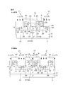
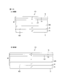
- FIG. 1A and 1B are schematic plan views of a trench gate type MIS transistor according to a first embodiment of the present invention.
- FIG. 1A is an overall view, and FIG. Each enlarged view is shown.
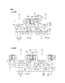
- FIG. 2 is a cross-sectional view of the trench gate type MIS transistor shown in FIGS. 1 (a) and 1 (b), and shows cross sections along the cutting lines AA and BB in FIG. 1 (b), respectively.
- 3A is a schematic cross-sectional view showing a part of the manufacturing process of the trench gate type MIS transistor shown in FIG. 2, and shows a cut surface at the same position as FIG.
- FIG. 3B is a diagram showing a step subsequent to FIG. 3A.
- FIG. 3C is a diagram showing a step subsequent to FIG. 3B.
- FIG. 3D is a diagram showing a step subsequent to FIG. 3C.
- FIG. 3E is a diagram showing a step subsequent to that in FIG. 3D.
- FIG. 3F is a diagram showing a step subsequent to that in FIG. 3E.
- FIG. 3G is a diagram showing a step subsequent to FIG. 3F.
- FIG. 3H is a diagram showing a step subsequent to that in FIG. 3G.
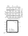
- FIG. 4 is a schematic cross-sectional view showing a first modification of the trench gate type MIS transistor shown in FIG. 5A and 5B are schematic plan views showing a second modified example of the trench gate type MIS transistor shown in FIG. 2, wherein FIG. 5A is an overall view, and FIG. Each internal enlarged view is shown.
- FIG. 5A is an overall view
- FIG. Each internal enlarged view is shown.
- FIG. 6 is a cross-sectional view of the trench gate type MIS transistor shown in FIGS. 5A and 5B, and shows a cut surface taken along the section line CC in FIG. 5B.
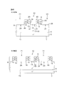
- FIG. 7 is a cross-sectional view of a trench gate type MIS transistor according to a second embodiment of the present invention, and shows a cut surface at the same position as FIG. 8A is a schematic cross-sectional view showing a part of the manufacturing process of the trench gate type MIS transistor shown in FIG. 7, and shows a cut surface at the same position as FIG.
- FIG. 8B is a diagram showing a step subsequent to FIG. 8A.
- FIG. 8C is a diagram showing a step subsequent to FIG. 8B.
- FIG. 8D is a diagram showing a step subsequent to FIG.
- FIG. 8E is a diagram showing a step subsequent to that in FIG. 8D.
- FIG. 8F is a diagram showing a step subsequent to that in FIG. 8E.
- FIG. 8G is a diagram showing a step subsequent to FIG. 8F.
- FIG. 8H is a diagram showing a step subsequent to FIG. 8G.
- FIG. 8I is a diagram showing a step subsequent to that in FIG. 8H.
- FIG. 9 is a schematic cross-sectional view showing a modification of the trench gate type MIS transistor shown in FIG.
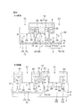
- FIG. 10 is a cross-sectional view of a trench gate type MIS transistor according to a third embodiment of the present invention, and shows a cut surface at the same position as FIG.
- FIG. 11A is a schematic cross-sectional view showing a part of the manufacturing process of the trench gate type MIS transistor shown in FIG. 10, and shows a cut surface at the same position as FIG.
- FIG. 11B is a diagram showing a step subsequent to FIG. 11A.
- FIG. 11C is a diagram showing a step subsequent to FIG. 11B.
- FIG. 11D is a diagram showing a step subsequent to that in FIG. 11C.
- FIG. 11E is a diagram showing a step subsequent to FIG. 11D.
- FIG. 11F is a diagram showing a step subsequent to that in FIG. 11E.
- FIG. 11G is a diagram showing a step subsequent to that in FIG. 11F.
- FIG. 11H is a diagram showing a step subsequent to FIG. 11G.
- FIG. 12 is a schematic cross-sectional view showing a modification of the trench gate type MIS transistor shown in FIG.
- FIG. 1A and 1B are schematic plan views of a trench gate type MIS transistor according to a first embodiment of the present invention.
- FIG. 1A is an overall view, and FIG. Each enlarged view is shown.
- FIG. 2 is a cross-sectional view of the trench gate type MIS transistor shown in FIGS. 1 (a) and 1 (b), and shows cross sections along the cutting lines AA and BB in FIG. 1 (b), respectively.
- the MIS transistor 1 is a trench gate type DMISFET (Double-diffused Metal-Insulator-Semiconductor-Field-Effect-Transistor) employing SiC, and has, for example, a square chip shape in plan view as shown in FIG.
- the chip-like MIS transistor 1 has a length of about several millimeters in the vertical and horizontal directions on the paper surface of FIG.
- a source pad 2 is formed on the surface of the MIS transistor 1.
- the source pad 2 has a substantially square shape in plan view with four corners curved outward, and is formed to cover almost the entire surface of the MIS transistor 1.
- the source pad 2 has a removal region 3 near the center of one side.
- the removal region 3 is a region where the source pad 2 is not formed.
- the MIS transistor 1 includes an n + type SiC substrate 5 (for example, the concentration is 1 ⁇ 10 18 to 1 ⁇ 10 21 cm ⁇ 3 ).
- the SiC substrate 5 functions as the drain of the MIS transistor 1, and its front surface 6 (upper surface) is a Si surface and its rear surface 7 (lower surface) is a C surface.
- an n ⁇ type SiC epitaxial layer 8 having a lower concentration than the SiC substrate 5 (for example, a concentration of 1 ⁇ 10 15 to 1 ⁇ 10 17 cm ⁇ 3 ) is laminated.
- the thickness of SiC epitaxial layer 8 as the semiconductor layer is, for example, 1 ⁇ m to 100 ⁇ m.
- the SiC epitaxial layer 8 is formed on the SiC substrate 5 by so-called epitaxial growth.
- the SiC epitaxial layer 8 formed on the surface 6 that is the Si surface is grown with the Si surface as the main growth surface. Therefore, the surface 9 of the SiC epitaxial layer 8 formed by the growth is a Si surface, like the surface 6 of the SiC substrate 5.
- the surface 9 of the SiC epitaxial layer 8 may be a C plane. If the surface 9 is a C plane, a bottom wall 19 (described later) of the gate trench 15 parallel to the surface 9 can be formed as a C plane. As a result, since the oxidation rate of the bottom wall 19 with respect to the side wall 18 of the gate trench 15 can be increased, the portion of the gate insulating film 22 on the bottom wall 19 can be made thicker. Therefore, since the electric field applied to the gate insulating film 22 at the bottom of the gate trench 15 can be relaxed, dielectric breakdown at the bottom of the gate trench 15 can be prevented.
- the MIS transistor 1 includes an active region 10 that functions as the MIS transistor 1 and is disposed in the center of the SiC epitaxial layer 8 in plan view, and a transistor peripheral region that surrounds the active region 10 11 is formed.
- body region 12 of p-type for example, the concentration is 1.0 ⁇ 10 16 cm ⁇ 3 to 1.0 ⁇ 10 19 cm ⁇ 3
- a large number are arranged in a matrix (matrix) at a constant pitch in the column direction.
- Each body region 12 has a square shape in plan view. For example, the length in the vertical and horizontal directions on the paper surface of FIG. 1B is about 7.2 ⁇ m.
- the body region 12 can be formed by ion implantation as in the process of FIG. 3A described later, or can be formed by epitaxial growth. In the case of forming by ion implantation, the channel length and the concentration of the body region 12 can be controlled with good in-plane uniformity, so that the characteristics can be stabilized and the yield can be improved.
- n ⁇ type drift region 13 in which the state as it is after epitaxial growth is maintained.
- an n + -type (for example, concentration of 1 ⁇ 10 18 to 1 ⁇ 10 21 cm ⁇ 3 ) source region 14 is formed in almost the entire region on the surface 9 side.
- Gate trenches 15 are formed in a lattice shape so as to surround each body region 12 from surface 9 of SiC epitaxial layer 8 through each source region 14 and body region 12 to drift region 13.
- the gate trench 15 includes a linear portion 16 extending linearly in each of the row direction and the column direction along the four side surfaces of each body region 12 between the adjacent body regions 12, The linear part 16 extended in the direction and the cross part 17 where the linear part 16 extended in the column direction cross
- the intersecting portion 17 is surrounded by the inner corners of the four arranged body regions 12 and is defined by the extended lines of the four sides of the body region 12. This is a square portion in plan view.
- the gate trench 15 has a U-shaped cross section in which a side wall 18 and a bottom wall 19 facing each other are continuous via a curved surface.
- a large number of rectangular parallelepiped unit cells 21 having four corners 20 are formed in each window portion surrounded by the lattice-like gate trench 15.
- the depth direction of the gate trench 15 is the gate length direction
- the circumferential direction of each unit cell 21 orthogonal to the gate length direction is the gate width direction.
- a gate insulating film 22 made of SiO 2 is formed on the inner surface of the gate trench 15 so as to cover the entire area.
- the gate insulating film 22 does not appear strictly in FIG. 2, the portion of the gate insulating film 22 on the bottom wall 19 is thicker than the portion of the gate insulating film 22 on the side wall 18, and the top surface thereof is the body region 12. Or less than the deepest part (interface between the body region 12 and the drift region 13). Specifically, the thickness of the portion on the side wall 18 is about 1000 mm while the thickness of the portion on the bottom wall 19 is 1500 to 3000 mm. Thereby, since the electric field applied to the gate insulating film 22 at the bottom of the gate trench 15 can be relaxed, dielectric breakdown at the bottom of the gate trench 15 can be prevented.
- a vertical MIS transistor structure is configured in which the source region 14 and the drift region 13 are spaced apart from each other via the body region 12 in the vertical direction perpendicular to the surface 9 of the SiC epitaxial layer 8.
- a source trench 24 having a square shape in plan view is formed in the center of each unit cell 21 from the surface 9 of the SiC epitaxial layer 8 through the source region 14 and the body region 12 to reach the drift region 13. Yes.
- the depth of the source trench 24 is the same as that of the gate trench 15 in this embodiment.
- the source trench 24 also has a U-shaped cross section in which a side wall 25 and a bottom wall 26 facing each other are continuous via a curved surface.
- the gate breakdown voltage holding region 27 is formed along the lattice-shaped gate trench 15, and a first region 29 as a first breakdown voltage holding region formed at the intersection 17 of the gate trench 15 and the line of the gate trench 15. It integrally includes a second region 30 as a second breakdown voltage holding region formed in the shape portion 16.
- the first region 29 is a corner edge of the gate trench 15 formed at the bottom of the bottom wall 19 of the gate trench 15 at the intersection 17 and the corners 20 of the four unit cells 21 facing the intersection 17 from the bottom wall 19.
- the portion 31 is formed so as to reach the body region 12 immediately above the corner edge portion 31. That is, the first region 29 is formed in a square shape slightly larger than the intersecting portion 17 of the gate trench 15 in plan view, and each corner of each of the four unit cells 21 facing the intersecting portion 17 is formed. It has entered each part 20.
- the concentration of the first region 29 is higher than the concentration of the body region 12 and higher than the concentration of the drift region 13, for example, 1 ⁇ 10 17 to 9 ⁇ 10 19 cm ⁇ 3 .
- the thickness T 1 along the direction from the bottom surface of the gate trench 15 toward the SiC substrate 5 in the first region 29 is, for example, about 0.8 ⁇ m.
- the second region 30 is formed in a straight line having a constant width that connects the centers of the sides of the intersecting portions 17 adjacent in plan view, and the width of the linear portion 16 (the distance between the side surfaces of the gate trenches 15 facing each other (
- the width of the second region 30 is higher than that of the body region 12 and higher than that of the first region 29.
- the second thickness T 2 along the direction from the bottom of the gate trench 15 to SiC substrate 5 in the second region 30, the thickness of the first region 29 T 1 (ie, T 1 > T 2 ), for example, about 0.7 ⁇ m.
- the source breakdown voltage holding region 28 passes through the bottom wall 26 of the source trench 24 and the edge portion 32 of the source trench 24 where the bottom wall 26 and the side wall 25 intersect, and the body region 12 that forms a part of the side wall 25 of the source trench 24. It is formed to reach.
- the concentration of the source breakdown voltage holding region 28 is the same as that of the first region 29 of the gate breakdown voltage holding region 27 (for example, 1 ⁇ 10 17 to 9 ⁇ 10 19 cm ⁇ 3 .
- Thickness T 3 along the direction from the bottom surface of trench 24 toward SiC substrate 5 is the same as thickness T 1 of first region 29 of gate breakdown voltage holding region 27 (for example, about 0.8 ⁇ m).
- a p + -type body contact region 33 (for example, an impurity concentration of 1.0 ⁇ 10 18 cm ⁇ 3 to 2.0 ⁇ 10 21 cm ⁇ 3 ).
- a p-type guard ring is provided on the surface layer portion of the SiC epitaxial layer 8 at a distance from the active region 10 so as to surround the unit cells 21 (active regions 10) arranged in a matrix.
- a plurality of 34 are formed (four in this embodiment). These guard rings 34 can be formed by the same ion implantation step as the step of forming the p-type body region 12.
- Each guard ring 34 is formed in a square shape in plan view along the outer periphery of the MIS transistor 1 in plan view.
- An interlayer insulating film 35 made of SiO 2 is laminated on the SiC epitaxial layer 8 so as to cover the gate electrode 23.
- a contact hole 36 having a diameter larger than that of the source trench 24 is formed in the interlayer insulating film 35 and the gate insulating film 22. Thereby, in the contact hole 36, the entire source trench 24 of each unit cell 21 (that is, the side wall 25 and the bottom wall 26 of the source trench 24) and the peripheral portion of the source trench 24 on the surface 9 of the SiC epitaxial layer 8 are formed. It is exposed, and a step according to the height difference between the surface 9 and the bottom wall 26 is formed.
- a source electrode 37 is formed on the interlayer insulating film 35.
- the source electrode 37 collectively enters the source trenches 24 of all the unit cells 21 through the contact holes 36.
- the body contact region 33, the source It is in contact with the breakdown voltage holding region 28, the body region 12 and the source region 14. That is, the source electrode 37 is a common wiring for all the unit cells 21.
- An interlayer insulating film (not shown) is formed on the source electrode 37, and the source electrode 37 is connected to the source pad 2 (see FIG. 1A) via the interlayer insulating film (not shown). ) Is electrically connected.
- the gate pad 4 (see FIG. 1A) is electrically connected to the gate electrode 23 through a gate wiring (not shown) routed on the interlayer insulating film (not shown). ing.
- the source electrode 37 has a structure in which, for example, a Ti / TiN layer and an Al layer are laminated in order from the contact side with the SiC epitaxial layer 8.
- a drain electrode 38 is formed on the back surface 7 of the SiC substrate 5 so as to cover the entire area.
- the drain electrode 38 is a common electrode for all the unit cells 21.
- As the drain electrode 38 for example, a laminated structure (Ti / Ni / Au / Ag) in which Ti, Ni, Au, and Ag are laminated in this order from the SiC substrate 5 side can be applied.
- FIG. 3A to 3H are schematic cross-sectional views showing a part of the manufacturing process of the trench gate type MIS transistor shown in FIG. 2, and show a cut surface at the same position as FIG.
- an n-type impurity for example, N-type
- Si surface the surface 6 (Si surface) of the SiC substrate 5 by an epitaxial growth method such as a CVD method, an LPE method, or an MBE method.
- SiC crystal is grown while doping (nitrogen), P (phosphorus), As (arsenic), etc.).
- n ⁇ type SiC epitaxial layer 8 is formed on SiC substrate 5.
- p-type impurities for example, Al (aluminum), B (boron), etc.
- n-type impurities are implanted into the SiC epitaxial layer 8 from the surface 9 of the SiC epitaxial layer 8.
- the SiC epitaxial layer 8 is heat-treated at 1400 ° C. to 2000 ° C. Thereby, ions of p-type impurity and n-type impurity implanted into the surface layer portion of SiC epitaxial layer 8 are activated, and body region 12, source region 14 and guard ring 34 are simultaneously formed according to the implanted locations. Is done. In addition, a drift region 13 that maintains the state after epitaxial growth is formed in the base layer portion of SiC epitaxial layer 8.
- the SiC epitaxial layer 8 is etched using a mask having openings in regions where the gate trench 15 and the source trench 24 are to be formed. Thereby, SiC epitaxial layer 8 is dry-etched from surface 9 (Si surface), and gate trench 15 and source trench 24 are simultaneously formed. At the same time, a large number of unit cells 21 are formed in the SiC epitaxial layer 8.
- the etching gas includes, for example, a mixed gas (SF 6 / O 2 gas) containing SF 6 (sulfur hexafluoride) and O 2 (oxygen), SF 6 , O 2, and HBr (hydrogen bromide).
- a mixed gas (SF 6 / O 2 / HBr gas) can be used.
- a first resist 39 having an opening exposing the intersection 17 of the gate trench 15 and the source trench 24 is formed on the SiC epitaxial layer 8.
- p-type impurities are implanted (implanted) toward the intersection 17 and the source trench 24 of the gate trench 15 exposed from the opening of the first resist 39.
- the p-type impurity is also implanted into the sidewalls 18 and 25. It becomes.
- SiC epitaxial layer 8 is heat-treated at 1400 ° C. to 2000 ° C. As a result, ions of the p-type impurity implanted into the drift region 13 are activated, and the first region 29 of the gate breakdown voltage holding region 27 and the source breakdown voltage holding region 28 are formed simultaneously.
- a second resist 40 having openings in regions where the second region 30 and the body contact region 33 of the gate breakdown voltage holding region 27 are to be formed is formed on the SiC epitaxial layer 8.
- the side walls 18 and the bottom wall 19 of the intersecting portion 17 of the gate trench 15 and the peripheral portions of the side walls 25 and the bottom wall 26 of the source trench 24 are covered with the second resist 40.
- p-type impurities are implanted (implanted) toward the linear portion 16 of the gate trench 15 exposed from the opening of the second resist 40 and the central portion of the bottom wall 26 of the source trench 24.
- SiC epitaxial layer 8 is heat-treated at 1400 ° C. to 2000 ° C.
- ions of the p-type impurity implanted into the drift region 13 are activated, and the second region 30 and the body contact region 33 of the gate breakdown voltage holding region 27 are formed simultaneously.
- a SiO 2 material is deposited from above the SiC epitaxial layer 8 by a CVD method. Thereby, the gate insulating film 22 is formed.
- a doped polysilicon material is deposited from above the SiC epitaxial layer 8 by CVD. The deposition of the polysilicon material is continued until at least the gate trench 15 and the source trench 24 are filled. Thereafter, the deposited polysilicon material is etched back until the etch-back surface is flush with the surface 9 of the SiC epitaxial layer 8. Subsequently, only the polysilicon material remaining in the source trench 24 is removed by dry etching. Thereby, the gate electrode 23 made of the polysilicon material remaining in the gate trench 15 is formed.
- a SiO 2 material is deposited from above the SiC epitaxial layer 8 by a CVD method.
- the interlayer insulating film 35 is formed.
- the interlayer insulating film 35 and the gate insulating film 22 are successively patterned by a known patterning technique. As a result, contact holes 36 are formed in the interlayer insulating film 35 and the gate insulating film 22.
- the source electrode 37, the drain electrode 38, and the like are formed, whereby the MIS transistor 1 shown in FIG. 2 is obtained.
- a drain voltage is applied between the source pad 2 (source electrode 37) and the drain electrode 38 (between the source and drain) with the source pad 2 grounded (that is, the source electrode 37 is 0 V). Is done.
- a voltage equal to or higher than the gate threshold voltage is applied to the gate pad 4 (gate electrode 23)
- a channel is formed along the body region 12 that forms the side wall of each unit cell 21.
- a current flows from the drain electrode 38 to the source electrode 37, and each unit cell 21 is turned on.
- each unit cell 21 is turned off (that is, the gate voltage is 0 V) and the voltage is applied between the source and the drain, the unit cell 21 is interposed between the gate electrode 23 and the SiC epitaxial layer 8.
- An electric field is applied to the gate insulating film 22. This electric field is generated due to a potential difference between the gate electrode 23 and the SiC epitaxial layer 8.
- equipotential surfaces with a very high potential are distributed with the gate electrode 23 as a reference (0 V), and the interval between the equipotential surfaces is small, so a very large electric field is generated.
- an equipotential surface of 900 V is distributed in the vicinity of the back surface 7 of the SiC substrate 5 that is in contact with the drain electrode 38, and from the back surface 7 of the SiC substrate 5 to the surface 9 side of the SiC epitaxial layer 8.
- a voltage drop occurs as it goes, an equipotential surface of about several tens of volts is distributed in the vicinity of the bottom wall 19 of the gate trench 15. Therefore, a very large electric field is generated on the bottom wall 19 of the gate trench 15 toward the gate electrode 23 side.
- the gate trenches 15 are formed in a lattice shape and the rectangular columnar unit cells 21 are arranged in the windows of the lattice-like gate trenches 15, each of the unit cells 21 In the vicinity of the corner edge portion 31 of the gate trench 15 formed in the corner portion 20, the dielectric breakdown of the gate insulating film 22 is particularly likely to occur.
- the distance D 1 (see the AA cross section in FIG. 2) of the source trenches 24 adjacent to each other on the diagonal line of the intersecting portion 17 of the gate trench 15 is equal to each other across the linear portion 16 of the gate trench 15. It becomes larger than the distance D 2 (see the BB cross section in FIG. 2) between the adjacent source trenches 24 (for example, in this embodiment, D 1 is 1.4 times D 2 ). Therefore, an equipotential surface enters directly under the corner edge portion 31 of the gate trench 15 having a relatively wide space, and the equipotential surfaces are densely formed. As a result, the dielectric breakdown of the gate insulating film 22 is particularly likely to occur near the corner edge portion 31 of the gate trench 15.
- the gate breakdown voltage holding region 27 (first region 29) is formed at the corner edge portion 31 of the gate trench 15.
- a depletion layer generated by the junction (pn junction) between the first region 29 and the drift region 13 can be generated in the vicinity of the corner edge portion 31 of the gate trench 15.
- a source breakdown voltage holding region 28 is formed at the edge portion 32 of the source trench 24 formed in the center portion of each unit cell 21. Therefore, a depletion layer generated by the junction (pn junction) between the source breakdown voltage holding region 28 and the drift region 13 can be expanded toward the corner edge portion 31 of the gate trench 15 surrounding the source trench 24.
- the first region 29 is formed so as to reach the body region 12 immediately above the corner edge portion 31 through the corner edge portion 31, but a channel is formed in the corner portion 20 of the unit cell 21. It is not formed or even if it is formed, the current flowing through the channel is very small. Therefore, by forming the gate breakdown voltage holding region 27 (first region 29) so as to reach the portion of the body region 12 immediately above the corner edge portion 31, the performance of the gate insulating film 22 is hardly affected. The destruction prevention effect can be further improved.
- a gate breakdown voltage holding region 27 (second region 30) having a width narrower than the width of the linear portion 16 is formed in the linear portion 16 of the gate trench 15.
- a depletion layer generated by the junction (pn junction) between the second region 30 and the drift region 13 can be generated along the linear portion 16 of the gate trench 15. Therefore, the electric field generated immediately below the linear portion 16 of the gate trench 15 can be relaxed by the depletion layer. As a result, the electric field generated in the gate insulating film 22 can be alleviated uniformly.
- the gate breakdown voltage holding region 27 (second region 30) is not formed on the side wall 18 of the linear portion 16 of the gate trench 15 (that is, the portion where the channel is formed in the unit cell 21). Therefore, the channel characteristics can be controlled with high accuracy. Further, the concentration of the second region 30 is higher than the concentration of the first region 29, and the thickness T 2 of the second region 30 is smaller than the thickness T 1 of the first region 29 (T 1 > T 2 ). Therefore, an increase in channel resistance can be prevented.
- FIG. 7 is a cross-sectional view of a trench gate type MIS transistor according to a second embodiment of the present invention, and shows a cut surface at the same position as FIG.
- parts corresponding to the respective parts shown in FIG. 2 are denoted by the same reference numerals as those given to the respective parts, and description thereof will be omitted.
- the drift region 13 is formed only by a low-concentration n ⁇ -type region (for example, a concentration of 1 ⁇ 10 15 to 1 ⁇ 10 17 cm ⁇ 3 ).
- the drift region 72 of the MIS transistor 71 according to the embodiment has a structure in which two layers having different impurity concentrations are stacked along the thickness direction of the SiC epitaxial layer 8, and is a lower layer in contact with the surface 6 of the SiC substrate 5.
- An n ⁇ type low concentration region 73 as an example of the second region on the side, and an n type high concentration region 74 as an example of the first region on the upper layer side formed on the low concentration region 73 are included.
- the concentration of the low concentration region 73 is, for example, 1 ⁇ 10 15 to 1 ⁇ 10 17 cm ⁇ 3
- the concentration of the high concentration region 74 is, for example, 2 ⁇ 10 15 to 1 ⁇ 10 18 cm ⁇ 3 .
- the interface 75 between the low concentration region 73 and the high concentration region 74 (the upper end of the low concentration region 73) is a level difference caused by a part of the surface of the SiC epitaxial layer 8 being lowered due to the formation of the gate trench 15 and the source trench 24. It undulates together.
- the high concentration region 74 on the surface 9 side is formed so as to form the surface 9 of the SiC epitaxial layer 8, the side wall 18 and the bottom wall 19 of the gate trench 15, and the side wall 25 and the bottom wall 26 of the source trench 24.
- the low concentration region 73 has a low step portion 76 in each unit cell 21, for example, at a portion facing the bottom wall 19 of the gate trench 15 and the bottom wall 26 of the source trench 24. 9)
- a high step portion 77 is provided at a portion facing the portion 9).
- the lengths T 4 , T 5 and T 6 are uniform. These thicknesses T 4 , T 5 , and T 6 are larger than the thicknesses T 1 and T 2 of the gate breakdown voltage holding region 27 and the thickness T 3 of the source breakdown voltage holding region 28.
- the gate breakdown voltage holding region 27 (first region 29 and second region 30) and the source breakdown voltage holding region 28 are covered with the high concentration region 74.
- FIGS. 8A to 8I are schematic cross-sectional views showing a part of the manufacturing process of the trench gate type MIS transistor shown in FIG. 7 in the order of steps, and show a cut surface at the same position as FIG.
- an n ⁇ type SiC epitaxial layer 8 is formed on SiC substrate 5 by performing the same process as in FIGS. 3A to 3B.
- the body region 12, the source region 14, the guard ring 34 and the drift region 72 are simultaneously formed. Thereafter, SiC epitaxial layer 8 is dry-etched from surface 9 (Si surface), and gate trench 15 and source trench 24 are formed simultaneously.
- the n-type impurity is formed on the entire surface (including the bottom surfaces of the gate trench 15 and the source trench 24).
- Implantation (injection) is performed inside the epitaxial layer 8.
- SiC epitaxial layer 8 is heat-treated at 1400 ° C. to 2000 ° C. Thereby, n-type impurity ions implanted into SiC epitaxial layer 8 are activated, and high concentration region 74 is formed above drift region 72.
- a low concentration region 73 that maintains the impurity concentration of the drift region 72 is formed below the drift region 72.
- FIGS. 8D to 8I steps similar to those in FIGS. 3C to 3H are performed, whereby the MIS transistor 71 shown in FIG. 7 is obtained.
- this MIS transistor 71 can exhibit the same effects as those of the MIS transistor 1 described above.
- a high concentration region 74 is formed, and this high concentration region 74 covers the gate breakdown voltage holding region 27 and the source breakdown voltage holding region 28.
- the pn junction between the gate breakdown voltage holding region 27 and the source breakdown voltage holding region 28 in the drift region 72 can be assigned to the high concentration region 74. Therefore, the spread of the depletion layer generated from the pn junction can be suppressed. As a result, the path of electrons flowing through the channel is not hindered by the depletion layer, and a sufficiently large path can be secured, so that an increase in on-resistance can be prevented.
- the thicknesses T 4 , T 5 , and T 6 of the high-concentration region 74 are the thicknesses T 1 and T 2 of the gate breakdown voltage holding region 27 and the source breakdown voltage holding region, as in the MIS transistor 78 of FIG. the thickness of 28 T 3 may be less.
- each bottom portion of the gate breakdown voltage holding region 27 and the source breakdown voltage holding region 28 protrudes toward the low concentration region 73 with respect to the interface 75 and is covered with the low concentration region 73.
- Such a configuration can be formed by performing ion implantation at the time of forming the high concentration region 74 with lower energy than in the case of the MIS transistor 71. Therefore, the high concentration region 74 can be easily formed with low energy.
- FIG. 10 is a cross-sectional view of a trench gate type MIS transistor according to a third embodiment of the present invention, and shows a cut surface at the same position as FIG. 10, parts corresponding to the parts shown in FIG. 2 are denoted by the same reference numerals as those given to the respective parts, and description thereof will be omitted.
- the drift region 13 is formed only by a low-concentration n ⁇ -type region (for example, a concentration of 1 ⁇ 10 15 to 1 ⁇ 10 17 cm ⁇ 3 ).
- the drift region 82 of the MIS transistor 81 according to the embodiment has a structure in which two layers having different impurity concentrations are stacked along the thickness direction of the SiC epitaxial layer 8.
- n ⁇ type low concentration region 83 as an example of a lower second region in contact with the surface 6 of the substrate 5, and an n type high concentration as an example of an upper layer first region formed on the low concentration region 83.
- the concentration of the low concentration region 83 is, for example, 1 ⁇ 10 15 to 1 ⁇ 10 17 cm ⁇ 3
- the concentration of the high concentration region 84 is, for example, 2 ⁇ 10 15 to 1 ⁇ 10 18 cm ⁇ 3 .
- High concentration region 84 is formed to form surface 9 of SiC epitaxial layer 8, sidewall 18 and bottom wall 19 of gate trench 15, and sidewall 25 and bottom wall 26 of source trench 24. Further, the interface 85 (the upper end of the low concentration region 83) between the low concentration region 83 and the high concentration region 84 is generated by a part of the surface of the SiC epitaxial layer 8 being lowered due to the formation of the gate trench 15 and the source trench 24. Regardless of the level difference, the height is constant along the top (surface 9) of the unit cell 21.
- T 7 , T 8 , and T 9 Due to the constant height of the interface 75, the thickness in the high concentration region 84 along the direction from the top (surface 9) of the unit cell 21, the bottom of the gate trench 15, and the bottom of the source trench 24 toward the SiC substrate 5.
- the thicknesses T 8 and T 9 of the high concentration region 84 are larger than the thicknesses T 1 and T 2 of the gate breakdown voltage holding region 27 and the thickness T 3 of the source breakdown voltage holding region 28.
- the gate breakdown voltage holding region 27 (first region 29 and second region 30) and the source breakdown voltage holding region 28 are covered with the high concentration region 74.
- 11A to 11H are schematic cross-sectional views showing a part of the manufacturing process of the trench gate type MIS transistor shown in FIG. 10, and show a cut surface at the same position as FIG.
- an n-type impurity is doped on the surface 6 (Si surface) of the SiC substrate 5 by an epitaxial growth method such as a CVD method, an LPE method, or an MBE method.
- a SiC crystal is grown (for example, the concentration is 1 ⁇ 10 15 to 1 ⁇ 10 17 cm ⁇ 3 ).
- n ⁇ type low concentration region 83 is formed on SiC substrate 5.
- the dose is increased (for example, 2 ⁇ 10 15 to 1 ⁇ 10 19 cm ⁇ 3 ), and an SiC crystal is further grown while doping the n-type impurity. Thereby, high concentration region 84 is formed, and SiC epitaxial layer 8 is formed.
- SiC epitaxial layer 8 is heat-treated at 1400 ° C. to 2000 ° C. Thereby, ions of p-type impurity and n-type impurity implanted into the surface layer portion of SiC epitaxial layer 8 are activated, and body region 12, source region 14 and guard ring 34 are simultaneously formed according to the implanted locations. Is done.
- the gate trench 15 and the source trench 24 are formed at the same time, with the deepest part reaching the middle part in the thickness direction of the high-concentration region 84 by performing the same process as in FIG. 3B.
- the first resist 39 having an opening exposing the intersection 17 of the gate trench 15 and the source trench 24 is formed on the SiC epitaxial layer 8. Formed.
- FIGS. 11D to 11F by performing the same process as in FIGS. 3D to 3F, the deepest portion reaches the middle of the high concentration region 84 in the thickness direction, respectively.
- the first region 29, the source breakdown voltage holding region 28, the second region 30 of the gate breakdown voltage holding region 27, and the body contact region 33 are formed.
- MIS transistor 81 shown in FIG. 10 is obtained by performing the same processes as in FIGS. 3G to 3H.
- this MIS transistor 81 can exhibit the same effects as those of the MIS transistor 1 described above. Further, in the MIS transistor 81, the bottom wall 19 of the gate trench 15 in which the p-type gate breakdown voltage holding region 27 is formed, and the bottom wall 26 of the source trench 24 in which the p-type source breakdown voltage holding region 28 is formed. Thus, a high concentration region 84 is formed, and this high concentration region 84 covers the gate breakdown voltage holding region 27 and the source breakdown voltage holding region 28.
- the pn junction between the gate breakdown voltage holding region 27 and the source breakdown voltage holding region 28 in the drift region 82 can be assigned to the high concentration region 84. Therefore, the spread of the depletion layer generated from the pn junction can be suppressed. As a result, the path of electrons flowing through the channel is not hindered by the depletion layer, and a sufficiently large path can be secured, so that an increase in on-resistance can be prevented.
- the thicknesses T 8 and T 9 of the high concentration region 84 are the thicknesses T 1 and T 2 of the gate breakdown voltage holding region 27 and the thickness of the source breakdown voltage holding region 28 as in the MIS transistor 86 of FIG. it may be a T 3 below.
- each bottom portion of the gate breakdown voltage holding region 27 and the source breakdown voltage holding region 28 protrudes toward the low concentration region 83 with respect to the interface 85 and is covered with the low concentration region 83.
- this invention can also be implemented with another form.
- a configuration in which the conductivity type of each semiconductor portion of the MIS transistors 1, 41, 51, 71, 78, 81, 86 is inverted may be employed.
- the p-type portion may be n-type and the n-type portion may be p-type.
- the layers constituting the semiconductor layers are not limited to SiC epitaxial layers, but wide band gap semiconductors other than SiC, such as GaN (band gaps).
- Eg GaN about 3.4eV)
- may be a layer consisting of diamond (band gap Eg dia about 5.5eV).
- the source trench 24 may be omitted.
- body contact region 33 can be formed so as to penetrate source region 14 and body region 12 from surface 9 of SiC epitaxial layer 8 to reach drift region 13.
- the arrangement of the body regions 12 is not limited to the matrix shape as shown in FIG. 1B, but is, for example, a stripe shape like the MIS transistors 51 shown in FIGS. 5A and 5B and FIG. There may be.
- a plurality of body contact regions 33 may be formed at intervals from each other along the longitudinal direction of the source trench 24.
- the gate breakdown voltage holding region 27 is formed along the linear gate trench 15 extending between the stripe-shaped body regions 12. Yes.
- the first region 29 of the gate breakdown voltage holding region 27 is formed at the end 52 of the gate trench 15.
- the second region 30 of the gate breakdown voltage holding region 27 is formed in the linear portion 53 of the gate trench 15.
- Each unit cell 21 is not limited to a rectangular parallelepiped shape (quadrangular columnar shape), and may be other polygonal columnar shapes such as a triangular prism shape, a pentagonal column shape, and a hexagonal column shape.
- the semiconductor power device of the present invention is, for example, a power used for an inverter circuit constituting a drive circuit for driving an electric motor used as a power source for an electric vehicle (including a hybrid vehicle), a train, an industrial robot, and the like. Can be incorporated into modules. It can also be incorporated into a power module used in an inverter circuit that converts electric power generated by a solar cell, wind power generator, or other power generation device (especially an in-house power generation device) to match the power of a commercial power source.
- Second region 31 ... (Gate trench ) Corner edge portion, 32... (Source trench) edge portion, 37... Source electrode, 38... Drain electrode, 41... MIS transistor, 51. Edge of gate trench, 53 ... Linear part of gate trench, 71 ... MIS transistor, 72 ... Drift region, 73 ... Low concentration region, 74 ... High concentration region, 75 ... Interface, 78 ... MIS transistor, 81 ... MIS transistor, 82 ... Drift region, 83 ... Low concentration region, 84 ... High concentration region, 85 ... Interface, 86 ... MIS transistors
Landscapes
- Electrodes Of Semiconductors (AREA)
Priority Applications (10)
| Application Number | Priority Date | Filing Date | Title |
|---|---|---|---|
| EP18204665.6A EP3460855A1 (de) | 2011-02-02 | 2012-02-01 | Halbleiterbauelement |
| US13/983,051 US9136322B2 (en) | 2011-02-02 | 2012-02-01 | Semiconductor device |
| EP12741475.3A EP2672517B8 (de) | 2011-02-02 | 2012-02-01 | Halbleitervorrichtung und herstellungsverfahren dafür |
| US14/821,056 US9620593B2 (en) | 2011-02-02 | 2015-08-07 | Semiconductor device |
| US15/441,850 US10068964B2 (en) | 2011-02-02 | 2017-02-24 | Semiconductor device |
| US16/050,794 US10680060B2 (en) | 2011-02-02 | 2018-07-31 | Semiconductor device |
| US16/865,267 US11133377B2 (en) | 2011-02-02 | 2020-05-01 | Semiconductor device |
| US17/464,296 US11804520B2 (en) | 2011-02-02 | 2021-09-01 | Semiconductor device |
| US18/472,704 US12581700B2 (en) | 2011-02-02 | 2023-09-22 | Semiconductor device |
| US19/433,326 US20260122984A1 (en) | 2011-02-02 | 2025-12-26 | Semiconductor device |
Applications Claiming Priority (4)
| Application Number | Priority Date | Filing Date | Title |
|---|---|---|---|
| JP2011-020730 | 2011-02-02 | ||
| JP2011020730 | 2011-02-02 | ||
| JP2011-101786 | 2011-04-28 | ||
| JP2011101786A JP5498431B2 (ja) | 2011-02-02 | 2011-04-28 | 半導体装置およびその製造方法 |
Related Child Applications (2)
| Application Number | Title | Priority Date | Filing Date |
|---|---|---|---|
| US13/983,051 A-371-Of-International US9136322B2 (en) | 2011-02-02 | 2012-02-01 | Semiconductor device |
| US14/821,056 Continuation US9620593B2 (en) | 2011-02-02 | 2015-08-07 | Semiconductor device |
Publications (1)
| Publication Number | Publication Date |
|---|---|
| WO2012105613A1 true WO2012105613A1 (ja) | 2012-08-09 |
Family
ID=46602819
Family Applications (1)
| Application Number | Title | Priority Date | Filing Date |
|---|---|---|---|
| PCT/JP2012/052293 Ceased WO2012105613A1 (ja) | 2011-02-02 | 2012-02-01 | 半導体装置およびその製造方法 |
Country Status (5)
| Country | Link |
|---|---|
| US (8) | US9136322B2 (de) |
| EP (2) | EP3460855A1 (de) |
| JP (1) | JP5498431B2 (de) |
| DE (1) | DE202012013628U1 (de) |
| WO (1) | WO2012105613A1 (de) |
Cited By (9)
| Publication number | Priority date | Publication date | Assignee | Title |
|---|---|---|---|---|
| WO2014030589A1 (ja) * | 2012-08-20 | 2014-02-27 | ローム株式会社 | 半導体装置 |
| WO2014061367A1 (ja) * | 2012-10-18 | 2014-04-24 | 三菱電機株式会社 | 炭化珪素半導体装置およびその製造方法 |
| WO2014115494A1 (en) * | 2013-01-25 | 2014-07-31 | Kabushiki Kaisha Toyota Chuo Kenkyusho | Method of manufacturing semiconductor device |
| WO2014178262A1 (ja) * | 2013-04-30 | 2014-11-06 | 日産自動車株式会社 | 半導体装置及びその製造方法 |
| US20160181372A1 (en) * | 2013-07-26 | 2016-06-23 | Sumitomo Electric Industries, Ltd. | Silicon carbide semiconductor device and method for manufacturing same |
| JP2018125331A (ja) * | 2017-01-30 | 2018-08-09 | 株式会社東芝 | 半導体装置及びその製造方法 |
| CN111540784A (zh) * | 2019-02-07 | 2020-08-14 | 瑞萨电子株式会社 | 半导体器件及制造半导体器件的方法 |
| WO2021085138A1 (ja) * | 2019-10-30 | 2021-05-06 | 株式会社デンソー | 炭化珪素半導体装置およびその製造方法 |
| JP2025509963A (ja) * | 2022-03-24 | 2025-04-11 | ウルフスピード インコーポレイテッド | トレンチ型半導体デバイスのための支持シールド構造 |
Families Citing this family (85)
| Publication number | Priority date | Publication date | Assignee | Title |
|---|---|---|---|---|
| JP2014099670A (ja) * | 2011-02-02 | 2014-05-29 | Rohm Co Ltd | 半導体装置およびその製造方法 |
| JP5498431B2 (ja) | 2011-02-02 | 2014-05-21 | ローム株式会社 | 半導体装置およびその製造方法 |
| KR101427925B1 (ko) * | 2012-11-15 | 2014-08-08 | 현대자동차 주식회사 | 반도체 소자 및 그 제조 방법 |
| JP2014131008A (ja) | 2012-11-29 | 2014-07-10 | Fuji Electric Co Ltd | ワイドバンドギャップ半導体装置 |
| JP6177812B2 (ja) * | 2013-02-05 | 2017-08-09 | 三菱電機株式会社 | 絶縁ゲート型炭化珪素半導体装置及びその製造方法 |
| JP6143490B2 (ja) | 2013-02-19 | 2017-06-07 | ローム株式会社 | 半導体装置およびその製造方法 |
| JP6164636B2 (ja) | 2013-03-05 | 2017-07-19 | ローム株式会社 | 半導体装置 |
| JP6164604B2 (ja) | 2013-03-05 | 2017-07-19 | ローム株式会社 | 半導体装置 |
| JP6077380B2 (ja) * | 2013-04-24 | 2017-02-08 | トヨタ自動車株式会社 | 半導体装置 |
| US9331197B2 (en) | 2013-08-08 | 2016-05-03 | Cree, Inc. | Vertical power transistor device |
| US10600903B2 (en) | 2013-09-20 | 2020-03-24 | Cree, Inc. | Semiconductor device including a power transistor device and bypass diode |
| US10868169B2 (en) * | 2013-09-20 | 2020-12-15 | Cree, Inc. | Monolithically integrated vertical power transistor and bypass diode |
| US20160211334A1 (en) * | 2013-10-04 | 2016-07-21 | Mitsubishi Electric Corporation | Silicon carbide semiconductor device and method for manufacturing same |
| US20150118810A1 (en) * | 2013-10-24 | 2015-04-30 | Madhur Bobde | Buried field ring field effect transistor (buf-fet) integrated with cells implanted with hole supply path |
| TWI532193B (zh) * | 2013-12-11 | 2016-05-01 | 節能元件控股有限公司 | 溝渠式金氧半p-n接面二極體結構及其製作方法 |
| JP6311723B2 (ja) * | 2013-12-16 | 2018-04-18 | 富士電機株式会社 | 半導体装置および半導体装置の製造方法 |
| JP6256148B2 (ja) * | 2014-03-27 | 2018-01-10 | 住友電気工業株式会社 | 炭化珪素半導体装置およびその製造方法 |
| JP2015207588A (ja) | 2014-04-17 | 2015-11-19 | ローム株式会社 | 半導体装置 |
| DE112014006726T5 (de) * | 2014-08-08 | 2017-03-23 | Hitachi, Ltd. | Halbleitervorrichtung, Leistungsmodul, Stromrichtvorrichtung, Fahrzeug und Schienenfahrzeug |
| WO2016080322A1 (ja) | 2014-11-18 | 2016-05-26 | ローム株式会社 | 半導体装置および半導体装置の製造方法 |
| KR101655153B1 (ko) | 2014-12-12 | 2016-09-22 | 현대자동차 주식회사 | 반도체 소자 및 그 제조 방법 |
| WO2016199546A1 (ja) | 2015-06-09 | 2016-12-15 | 三菱電機株式会社 | 電力用半導体装置 |
| JP6584857B2 (ja) | 2015-08-11 | 2019-10-02 | 株式会社東芝 | 半導体装置 |
| KR101807122B1 (ko) | 2015-09-02 | 2018-01-10 | 현대자동차 주식회사 | 반도체 소자의 제조 방법 |
| JP6453188B2 (ja) * | 2015-09-04 | 2019-01-16 | 株式会社豊田中央研究所 | 炭化珪素半導体装置 |
| WO2017043607A1 (ja) * | 2015-09-09 | 2017-03-16 | 住友電気工業株式会社 | 縦型炭化珪素半導体装置のトレンチのアニール処理装置、縦型炭化珪素半導体装置の製造方法および縦型炭化珪素半導体装置 |
| JP6478884B2 (ja) | 2015-09-11 | 2019-03-06 | 株式会社東芝 | 半導体装置 |
| JP6759563B2 (ja) | 2015-11-16 | 2020-09-23 | 富士電機株式会社 | 半導体装置および半導体装置の製造方法 |
| KR20170070505A (ko) | 2015-12-14 | 2017-06-22 | 현대자동차주식회사 | 반도체 소자 및 그 제조 방법 |
| KR101786668B1 (ko) * | 2015-12-14 | 2017-10-18 | 현대자동차 주식회사 | 반도체 소자 및 그 제조 방법 |
| JP6560142B2 (ja) * | 2016-02-26 | 2019-08-14 | トヨタ自動車株式会社 | スイッチング素子 |
| JP6560141B2 (ja) * | 2016-02-26 | 2019-08-14 | トヨタ自動車株式会社 | スイッチング素子 |
| JP6545362B2 (ja) | 2016-03-23 | 2019-07-17 | 三菱電機株式会社 | 半導体装置および半導体装置の製造方法 |
| JP6658257B2 (ja) * | 2016-04-22 | 2020-03-04 | 住友電気工業株式会社 | 炭化珪素半導体装置 |
| US10403712B2 (en) | 2016-06-02 | 2019-09-03 | Infineon Technologies Americas Corp. | Combined gate trench and contact etch process and related structure |
| KR101836258B1 (ko) * | 2016-07-05 | 2018-03-08 | 현대자동차 주식회사 | 반도체 소자 및 그 제조 방법 |
| CN109478567B (zh) * | 2016-07-15 | 2022-12-16 | 罗姆股份有限公司 | 半导体装置 |
| JP6919159B2 (ja) * | 2016-07-29 | 2021-08-18 | 富士電機株式会社 | 炭化珪素半導体装置および炭化珪素半導体装置の製造方法 |
| US10535657B2 (en) | 2016-08-22 | 2020-01-14 | Tc Lab, Inc. | High density vertical thyristor memory cell array with improved isolation |
| US10692863B2 (en) | 2016-09-30 | 2020-06-23 | Rohm Co., Ltd. | Semiconductor device and semiconductor package |
| JP6233539B1 (ja) | 2016-12-21 | 2017-11-22 | 富士電機株式会社 | 半導体装置および半導体装置の製造方法 |
| JP6731571B2 (ja) * | 2016-12-27 | 2020-07-29 | 株式会社デンソー | SiC−MOSFETの製造方法 |
| JP6673232B2 (ja) * | 2017-01-17 | 2020-03-25 | 株式会社デンソー | 炭化珪素半導体装置 |
| CN110709997B (zh) * | 2017-06-06 | 2023-02-28 | 三菱电机株式会社 | 半导体装置以及电力变换装置 |
| WO2019077878A1 (ja) * | 2017-10-17 | 2019-04-25 | 富士電機株式会社 | 炭化珪素半導体装置および炭化珪素半導体装置の製造方法 |
| JP2019083243A (ja) * | 2017-10-30 | 2019-05-30 | 株式会社東芝 | 半導体装置及びその製造方法 |
| DE112018006007B4 (de) * | 2017-11-24 | 2025-11-27 | Rohm Co., Ltd. | Halbleitervorrichtung |
| DE102017127848B4 (de) * | 2017-11-24 | 2024-10-17 | Infineon Technologies Ag | Siliziumcarbid-Halbleiterbauelement mit Randabschlussstruktur |
| JP7057555B2 (ja) * | 2017-11-29 | 2022-04-20 | 国立研究開発法人産業技術総合研究所 | 半導体装置 |
| DE102017128633B4 (de) | 2017-12-01 | 2024-09-19 | Infineon Technologies Ag | Siliziumcarbid-halbleiterbauelement mit grabengatestrukturen und abschirmgebieten |
| DE112018007106B4 (de) | 2018-02-19 | 2026-03-05 | Mitsubishi Electric Corporation | Siliciumcarbid-halbleitereinheit |
| DE102018108178A1 (de) * | 2018-04-06 | 2019-10-10 | Infineon Technologies Ag | Halbleiterbauelement mit Grabenstruktur und Herstellungsverfahren |
| JP6945036B2 (ja) * | 2018-05-24 | 2021-10-06 | ローム株式会社 | 半導体装置 |
| JP2018129558A (ja) * | 2018-05-24 | 2018-08-16 | ローム株式会社 | 半導体装置 |
| JP2019068096A (ja) * | 2018-12-20 | 2019-04-25 | ローム株式会社 | 半導体装置 |
| DE112019006587T5 (de) * | 2019-01-08 | 2021-12-23 | Mitsubishi Electric Corporation | Halbleitereinheit und leistungswandlereinheit |
| JP6808766B2 (ja) * | 2019-01-11 | 2021-01-06 | 株式会社東芝 | 半導体装置 |
| DE102019101304B4 (de) * | 2019-01-18 | 2023-04-27 | Infineon Technologies Dresden GmbH & Co. KG | Leistungshalbleitervorrichtung und Verfahren zum Bilden einer Leistungshalbleitervorrichtung |
| US10763356B1 (en) * | 2019-04-03 | 2020-09-01 | Genesic Semiconductor Inc. | Manufacture of power devices having inversion channel |
| DE212020000485U1 (de) * | 2019-05-22 | 2021-07-19 | Rohm Co., Ltd. | SiC-Halbleiterbauteil |
| JP7321820B2 (ja) * | 2019-08-02 | 2023-08-07 | 株式会社東芝 | 半導体装置、インバータ回路、駆動装置、車両、及び、昇降機 |
| JP7242467B2 (ja) * | 2019-08-02 | 2023-03-20 | 株式会社東芝 | 半導体装置、インバータ回路、駆動装置、車両、及び、昇降機 |
| JP7278914B2 (ja) * | 2019-09-13 | 2023-05-22 | 株式会社東芝 | 半導体装置、半導体装置の製造方法、インバータ回路、駆動装置、車両、及び、昇降機 |
| JP7278913B2 (ja) * | 2019-09-13 | 2023-05-22 | 株式会社東芝 | 半導体装置、半導体装置の製造方法、インバータ回路、駆動装置、車両、及び、昇降機 |
| CN111276545B (zh) * | 2020-02-12 | 2023-03-14 | 重庆伟特森电子科技有限公司 | 一种新型沟槽碳化硅晶体管器件及其制作方法 |
| CN115244711B (zh) * | 2020-04-17 | 2023-12-12 | Hrl实验室有限责任公司 | 垂直金刚石mosfet及其制造方法 |
| JP2020129675A (ja) * | 2020-04-21 | 2020-08-27 | ローム株式会社 | 半導体装置 |
| CN115668511A (zh) * | 2020-06-26 | 2023-01-31 | 罗姆股份有限公司 | 半导体装置 |
| US12094926B2 (en) * | 2020-08-14 | 2024-09-17 | Wolfspeed, Inc. | Sidewall dopant shielding methods and approaches for trenched semiconductor device structures |
| JP2023174547A (ja) * | 2020-08-31 | 2023-12-07 | ジェネシック セミコンダクタ インク. | 改良型パワーデバイスの設計と製造 |
| US12080790B2 (en) * | 2020-10-28 | 2024-09-03 | Wolfspeed, Inc. | Power semiconductor devices including angled gate trenches |
| CN114512403B (zh) * | 2020-11-16 | 2023-06-23 | 苏州东微半导体股份有限公司 | 半导体器件的制造方法 |
| US11810976B2 (en) * | 2021-02-18 | 2023-11-07 | Semiconductor Components Industries, Llc | Semiconductor device |
| CN116998020A (zh) * | 2021-03-22 | 2023-11-03 | 罗姆股份有限公司 | 半导体装置 |
| CN113363311A (zh) * | 2021-06-08 | 2021-09-07 | 西安电子科技大学 | 一种双沟槽SiC功率MOS器件 |
| DE102021121138B3 (de) * | 2021-08-13 | 2023-02-02 | Infineon Technologies Ag | Halbleitervorrichtungen und verfahren zum herstellen einer halbleitervorrichtung |
| CN114005869B (zh) * | 2021-11-05 | 2025-03-07 | 北京绿能芯创电子科技有限公司 | 碳化硅沟槽mosfet器件结构及加工方法 |
| CN114203825B (zh) * | 2021-12-13 | 2023-03-24 | 无锡新洁能股份有限公司 | 一种垂直型碳化硅功率mosfet器件及其制造方法 |
| JP7803420B2 (ja) * | 2022-08-19 | 2026-01-21 | 富士電機株式会社 | 炭化珪素半導体装置 |
| TWI865987B (zh) * | 2022-12-14 | 2024-12-11 | 尼克森微電子股份有限公司 | 功率元件及其製作方法 |
| CN116110957A (zh) * | 2023-04-17 | 2023-05-12 | 深圳平创半导体有限公司 | 一种SiC多级阶梯分裂栅沟槽MOSFET器件及其制作方法 |
| CN116721925B (zh) * | 2023-08-08 | 2024-02-09 | 深圳平创半导体有限公司 | 集成sbd的碳化硅sgt-mosfet及其制备方法 |
| US12369368B2 (en) * | 2023-09-13 | 2025-07-22 | Genesic Semiconductor Inc. | Semiconductor switching device |
| CN117832275A (zh) * | 2023-12-22 | 2024-04-05 | 东南大学 | 一种低导通电阻的功率器件及制造方法 |
| EP4704515A1 (de) * | 2024-08-29 | 2026-03-04 | Infineon Technologies Austria AG | Feldeffekttransistor mit isoliertem gate mit grabenstruktur |
Citations (8)
| Publication number | Priority date | Publication date | Assignee | Title |
|---|---|---|---|---|
| JPS6459868A (en) * | 1987-08-29 | 1989-03-07 | Fuji Electric Co Ltd | Semiconductor device having insulating gate |
| JPH1098188A (ja) * | 1996-08-01 | 1998-04-14 | Kansai Electric Power Co Inc:The | 絶縁ゲート半導体装置 |
| JP2004311716A (ja) * | 2003-04-07 | 2004-11-04 | Toshiba Corp | 絶縁ゲート型半導体装置 |
| JP2005285913A (ja) * | 2004-03-29 | 2005-10-13 | Sanyo Electric Co Ltd | 半導体装置およびその製造方法 |
| JP2008078174A (ja) * | 2006-09-19 | 2008-04-03 | Fuji Electric Holdings Co Ltd | トレンチゲート型炭化珪素半導体装置 |
| JP2008235546A (ja) * | 2007-03-20 | 2008-10-02 | Denso Corp | 炭化珪素半導体装置およびその製造方法 |
| JP2008294210A (ja) | 2007-05-24 | 2008-12-04 | Fuji Electric Device Technology Co Ltd | 炭化珪素半導体装置の製造方法 |
| JP2010219361A (ja) * | 2009-03-18 | 2010-09-30 | Toshiba Corp | 半導体装置及びその製造方法 |
Family Cites Families (33)
| Publication number | Priority date | Publication date | Assignee | Title |
|---|---|---|---|---|
| JP2606404B2 (ja) * | 1990-04-06 | 1997-05-07 | 日産自動車株式会社 | 半導体装置 |
| JP2912508B2 (ja) * | 1992-11-13 | 1999-06-28 | シャープ株式会社 | 縦型mosトランジスタの製造方法 |
| JP3259485B2 (ja) | 1993-12-03 | 2002-02-25 | 富士電機株式会社 | 炭化けい素たて型mosfet |
| KR100199997B1 (ko) * | 1995-09-06 | 1999-07-01 | 오카메 히로무 | 탄화규소 반도체장치 |
| US5821583A (en) * | 1996-03-06 | 1998-10-13 | Siliconix Incorporated | Trenched DMOS transistor with lightly doped tub |
| US5719409A (en) | 1996-06-06 | 1998-02-17 | Cree Research, Inc. | Silicon carbide metal-insulator semiconductor field effect transistor |
| WO1998026458A1 (en) * | 1996-12-11 | 1998-06-18 | The Kansai Electric Power Co., Inc. | Insulated gate semiconductor device |
| US6342709B1 (en) * | 1997-12-10 | 2002-01-29 | The Kansai Electric Power Co., Inc. | Insulated gate semiconductor device |
| JP2004055976A (ja) | 2002-07-23 | 2004-02-19 | Toyota Industries Corp | トレンチ構造を有する半導体装置 |
| JP4109565B2 (ja) * | 2003-03-31 | 2008-07-02 | ローム株式会社 | 半導体装置の製造方法および半導体装置 |
| JP4241158B2 (ja) | 2003-04-17 | 2009-03-18 | 三菱電機株式会社 | 半導体装置 |
| US7279743B2 (en) * | 2003-12-02 | 2007-10-09 | Vishay-Siliconix | Closed cell trench metal-oxide-semiconductor field effect transistor |
| GB0403934D0 (en) | 2004-02-21 | 2004-03-24 | Koninkl Philips Electronics Nv | Trench-gate semiconductor devices and the manufacture thereof |
| US7397084B2 (en) * | 2005-04-01 | 2008-07-08 | Semiconductor Components Industries, L.L.C. | Semiconductor device having enhanced performance and method |
| JP4453671B2 (ja) | 2006-03-08 | 2010-04-21 | トヨタ自動車株式会社 | 絶縁ゲート型半導体装置およびその製造方法 |
| US7476932B2 (en) * | 2006-09-29 | 2009-01-13 | The Boeing Company | U-shape metal-oxide-semiconductor (UMOS) gate structure for high power MOS-based semiconductor devices |
| US7589377B2 (en) * | 2006-10-06 | 2009-09-15 | The Boeing Company | Gate structure with low resistance for high power semiconductor devices |
| JP5210564B2 (ja) * | 2007-07-27 | 2013-06-12 | ルネサスエレクトロニクス株式会社 | 半導体装置 |
| JP2009033036A (ja) * | 2007-07-30 | 2009-02-12 | Hitachi Ltd | 半導体装置及びこれを用いた電気回路装置 |
| US20090272982A1 (en) * | 2008-03-03 | 2009-11-05 | Fuji Electric Device Technology Co., Ltd. | Trench gate type semiconductor device and method of producing the same |
| JP5721308B2 (ja) | 2008-03-26 | 2015-05-20 | ローム株式会社 | 半導体装置 |
| JP2010050161A (ja) * | 2008-08-19 | 2010-03-04 | Nec Electronics Corp | 半導体装置 |
| US8093653B2 (en) | 2008-10-01 | 2012-01-10 | Niko Semiconductor Co., Ltd. | Trench metal oxide-semiconductor transistor and fabrication method thereof |
| US8552535B2 (en) * | 2008-11-14 | 2013-10-08 | Semiconductor Components Industries, Llc | Trench shielding structure for semiconductor device and method |
| US8188484B2 (en) * | 2008-12-25 | 2012-05-29 | Rohm Co., Ltd. | Semiconductor device |
| US8188538B2 (en) | 2008-12-25 | 2012-05-29 | Rohm Co., Ltd. | Semiconductor device and method of manufacturing semiconductor device |
| JPWO2010119789A1 (ja) | 2009-04-13 | 2012-10-22 | ローム株式会社 | 半導体装置および半導体装置の製造方法 |
| JP2011020730A (ja) | 2009-07-21 | 2011-02-03 | Nittoh Kogaku Kk | 締結部材 |
| JP2011044513A (ja) | 2009-08-20 | 2011-03-03 | National Institute Of Advanced Industrial Science & Technology | 炭化珪素半導体装置 |
| JP2011101786A (ja) | 2009-10-16 | 2011-05-26 | Nihon Crc Corp | 固定用シート付きマット及びその固定方法並びに該マットの製造方法 |
| US8415671B2 (en) * | 2010-04-16 | 2013-04-09 | Cree, Inc. | Wide band-gap MOSFETs having a heterojunction under gate trenches thereof and related methods of forming such devices |
| WO2011133481A2 (en) * | 2010-04-20 | 2011-10-27 | Maxpower Semiconductor Inc. | Power mosfet with embedded recessed field plate and methods of fabrication |
| JP5498431B2 (ja) | 2011-02-02 | 2014-05-21 | ローム株式会社 | 半導体装置およびその製造方法 |
-
2011
- 2011-04-28 JP JP2011101786A patent/JP5498431B2/ja active Active
-
2012
- 2012-02-01 EP EP18204665.6A patent/EP3460855A1/de active Pending
- 2012-02-01 DE DE202012013628.3U patent/DE202012013628U1/de not_active Expired - Lifetime
- 2012-02-01 WO PCT/JP2012/052293 patent/WO2012105613A1/ja not_active Ceased
- 2012-02-01 US US13/983,051 patent/US9136322B2/en active Active
- 2012-02-01 EP EP12741475.3A patent/EP2672517B8/de active Active
-
2015
- 2015-08-07 US US14/821,056 patent/US9620593B2/en active Active
-
2017
- 2017-02-24 US US15/441,850 patent/US10068964B2/en active Active
-
2018
- 2018-07-31 US US16/050,794 patent/US10680060B2/en active Active
-
2020
- 2020-05-01 US US16/865,267 patent/US11133377B2/en active Active
-
2021
- 2021-09-01 US US17/464,296 patent/US11804520B2/en active Active
-
2023
- 2023-09-22 US US18/472,704 patent/US12581700B2/en active Active
-
2025
- 2025-12-26 US US19/433,326 patent/US20260122984A1/en active Pending
Patent Citations (8)
| Publication number | Priority date | Publication date | Assignee | Title |
|---|---|---|---|---|
| JPS6459868A (en) * | 1987-08-29 | 1989-03-07 | Fuji Electric Co Ltd | Semiconductor device having insulating gate |
| JPH1098188A (ja) * | 1996-08-01 | 1998-04-14 | Kansai Electric Power Co Inc:The | 絶縁ゲート半導体装置 |
| JP2004311716A (ja) * | 2003-04-07 | 2004-11-04 | Toshiba Corp | 絶縁ゲート型半導体装置 |
| JP2005285913A (ja) * | 2004-03-29 | 2005-10-13 | Sanyo Electric Co Ltd | 半導体装置およびその製造方法 |
| JP2008078174A (ja) * | 2006-09-19 | 2008-04-03 | Fuji Electric Holdings Co Ltd | トレンチゲート型炭化珪素半導体装置 |
| JP2008235546A (ja) * | 2007-03-20 | 2008-10-02 | Denso Corp | 炭化珪素半導体装置およびその製造方法 |
| JP2008294210A (ja) | 2007-05-24 | 2008-12-04 | Fuji Electric Device Technology Co Ltd | 炭化珪素半導体装置の製造方法 |
| JP2010219361A (ja) * | 2009-03-18 | 2010-09-30 | Toshiba Corp | 半導体装置及びその製造方法 |
Cited By (21)
| Publication number | Priority date | Publication date | Assignee | Title |
|---|---|---|---|---|
| US9911844B2 (en) | 2012-08-20 | 2018-03-06 | Rohm Co., Ltd. | Semiconductor device |
| US10580852B2 (en) | 2012-08-20 | 2020-03-03 | Rohm Co., Ltd. | Semiconductor device |
| US9368616B2 (en) | 2012-08-20 | 2016-06-14 | Rohm Co., Ltd. | Semiconductor device |
| US10312320B2 (en) | 2012-08-20 | 2019-06-04 | Rohm Co., Ltd. | Semiconductor device |
| WO2014030589A1 (ja) * | 2012-08-20 | 2014-02-27 | ローム株式会社 | 半導体装置 |
| US9954072B2 (en) | 2012-10-18 | 2018-04-24 | Mitsubishi Electric Corporation | Silicon-carbide semiconductor device and manufacturing method thereof |
| WO2014061367A1 (ja) * | 2012-10-18 | 2014-04-24 | 三菱電機株式会社 | 炭化珪素半導体装置およびその製造方法 |
| WO2014115494A1 (en) * | 2013-01-25 | 2014-07-31 | Kabushiki Kaisha Toyota Chuo Kenkyusho | Method of manufacturing semiconductor device |
| CN104919594A (zh) * | 2013-01-25 | 2015-09-16 | 丰田自动车株式会社 | 制造半导体器件的方法 |
| US9660046B2 (en) | 2013-01-25 | 2017-05-23 | Kabushiki Kaisha Toyota Chuo Kenkyusho | Method of manufacturing semiconductor device |
| CN104919594B (zh) * | 2013-01-25 | 2017-10-27 | 丰田自动车株式会社 | 制造半导体器件的方法 |
| JP5939448B2 (ja) * | 2013-04-30 | 2016-06-22 | 日産自動車株式会社 | 半導体装置及びその製造方法 |
| WO2014178262A1 (ja) * | 2013-04-30 | 2014-11-06 | 日産自動車株式会社 | 半導体装置及びその製造方法 |
| US20160181372A1 (en) * | 2013-07-26 | 2016-06-23 | Sumitomo Electric Industries, Ltd. | Silicon carbide semiconductor device and method for manufacturing same |
| US10192960B2 (en) * | 2013-07-26 | 2019-01-29 | Sumitomo Electric Industries, Ltd. | Silicon carbide semiconductor device and method for manufacturing same |
| JP2018125331A (ja) * | 2017-01-30 | 2018-08-09 | 株式会社東芝 | 半導体装置及びその製造方法 |
| CN111540784A (zh) * | 2019-02-07 | 2020-08-14 | 瑞萨电子株式会社 | 半导体器件及制造半导体器件的方法 |
| WO2021085138A1 (ja) * | 2019-10-30 | 2021-05-06 | 株式会社デンソー | 炭化珪素半導体装置およびその製造方法 |
| JP2021072359A (ja) * | 2019-10-30 | 2021-05-06 | 株式会社デンソー | 炭化珪素半導体装置およびその製造方法 |
| JP7272235B2 (ja) | 2019-10-30 | 2023-05-12 | 株式会社デンソー | 炭化珪素半導体装置およびその製造方法 |
| JP2025509963A (ja) * | 2022-03-24 | 2025-04-11 | ウルフスピード インコーポレイテッド | トレンチ型半導体デバイスのための支持シールド構造 |
Also Published As
| Publication number | Publication date |
|---|---|
| US20150349057A1 (en) | 2015-12-03 |
| US20200258977A1 (en) | 2020-08-13 |
| US20210399088A1 (en) | 2021-12-23 |
| US11133377B2 (en) | 2021-09-28 |
| US20240014258A1 (en) | 2024-01-11 |
| US20170170259A1 (en) | 2017-06-15 |
| JP5498431B2 (ja) | 2014-05-21 |
| EP3460855A1 (de) | 2019-03-27 |
| EP2672517B8 (de) | 2019-04-03 |
| EP2672517A4 (de) | 2014-08-13 |
| US9136322B2 (en) | 2015-09-15 |
| US9620593B2 (en) | 2017-04-11 |
| US11804520B2 (en) | 2023-10-31 |
| US10680060B2 (en) | 2020-06-09 |
| EP2672517A1 (de) | 2013-12-11 |
| DE202012013628U1 (de) | 2018-10-18 |
| JP2012178536A (ja) | 2012-09-13 |
| US20180337227A1 (en) | 2018-11-22 |
| US12581700B2 (en) | 2026-03-17 |
| US20260122984A1 (en) | 2026-04-30 |
| EP2672517B1 (de) | 2018-11-28 |
| US20130306983A1 (en) | 2013-11-21 |
| US10068964B2 (en) | 2018-09-04 |
Similar Documents
| Publication | Publication Date | Title |
|---|---|---|
| US12581700B2 (en) | Semiconductor device | |
| JP6090805B2 (ja) | 半導体装置およびその製造方法 | |
| US20250267902A1 (en) | Superjunction silicon carbide semiconductor device having parallel pn column structure with crystal defects | |
| JP6065335B2 (ja) | 半導体装置 | |
| US10727318B2 (en) | Semiconductor device VDMOS having a gate insulating film having a high dielectric constant portion contacting the drift region for relaxing an electric field generated in the gate insulating film | |
| JP5858934B2 (ja) | 半導体パワーデバイスおよびその製造方法 | |
| US8829608B2 (en) | Semiconductor device | |
| US9159846B2 (en) | SiC semiconductor device | |
| US10439060B2 (en) | Semiconductor device and method of manufacturing semiconductor device | |
| JP6763779B2 (ja) | 半導体装置および半導体装置の製造方法 | |
| JP2012059943A (ja) | 半導体装置 | |
| JP7290973B2 (ja) | 半導体装置 | |
| US20230246102A1 (en) | Superjunction semiconductor device | |
| JP5571306B2 (ja) | 半導体装置 |
Legal Events
| Date | Code | Title | Description |
|---|---|---|---|
| 121 | Ep: the epo has been informed by wipo that ep was designated in this application |
Ref document number: 12741475 Country of ref document: EP Kind code of ref document: A1 |
|
| WWE | Wipo information: entry into national phase |
Ref document number: 13983051 Country of ref document: US |
|
| NENP | Non-entry into the national phase |
Ref country code: DE |
|
| WWE | Wipo information: entry into national phase |
Ref document number: 2012741475 Country of ref document: EP |