WO2012111093A1 - キャリア寿命の測定方法および測定装置 - Google Patents
キャリア寿命の測定方法および測定装置 Download PDFInfo
- Publication number
- WO2012111093A1 WO2012111093A1 PCT/JP2011/053154 JP2011053154W WO2012111093A1 WO 2012111093 A1 WO2012111093 A1 WO 2012111093A1 JP 2011053154 W JP2011053154 W JP 2011053154W WO 2012111093 A1 WO2012111093 A1 WO 2012111093A1
- Authority
- WO
- WIPO (PCT)
- Prior art keywords
- light
- excitation
- carrier
- time
- modulation
- Prior art date
- Legal status (The legal status is an assumption and is not a legal conclusion. Google has not performed a legal analysis and makes no representation as to the accuracy of the status listed.)
- Ceased
Links
Images














Classifications
-
- H—ELECTRICITY
- H10—SEMICONDUCTOR DEVICES; ELECTRIC SOLID-STATE DEVICES NOT OTHERWISE PROVIDED FOR
- H10P—GENERIC PROCESSES OR APPARATUS FOR THE MANUFACTURE OR TREATMENT OF DEVICES COVERED BY CLASS H10
- H10P74/00—Testing or measuring during manufacture or treatment of wafers, substrates or devices
-
- G—PHYSICS
- G01—MEASURING; TESTING
- G01N—INVESTIGATING OR ANALYSING MATERIALS BY DETERMINING THEIR CHEMICAL OR PHYSICAL PROPERTIES
- G01N21/00—Investigating or analysing materials by the use of optical means, i.e. using sub-millimetre waves, infrared, visible or ultraviolet light
- G01N21/62—Systems in which the material investigated is excited whereby it emits light or causes a change in wavelength of the incident light
- G01N21/63—Systems in which the material investigated is excited whereby it emits light or causes a change in wavelength of the incident light optically excited
- G01N21/64—Fluorescence; Phosphorescence
- G01N21/6408—Fluorescence; Phosphorescence with measurement of decay time, time resolved fluorescence
-
- G—PHYSICS
- G01—MEASURING; TESTING
- G01N—INVESTIGATING OR ANALYSING MATERIALS BY DETERMINING THEIR CHEMICAL OR PHYSICAL PROPERTIES
- G01N21/00—Investigating or analysing materials by the use of optical means, i.e. using sub-millimetre waves, infrared, visible or ultraviolet light
- G01N21/62—Systems in which the material investigated is excited whereby it emits light or causes a change in wavelength of the incident light
- G01N21/63—Systems in which the material investigated is excited whereby it emits light or causes a change in wavelength of the incident light optically excited
- G01N21/64—Fluorescence; Phosphorescence
-
- G—PHYSICS
- G01—MEASURING; TESTING
- G01N—INVESTIGATING OR ANALYSING MATERIALS BY DETERMINING THEIR CHEMICAL OR PHYSICAL PROPERTIES
- G01N21/00—Investigating or analysing materials by the use of optical means, i.e. using sub-millimetre waves, infrared, visible or ultraviolet light
- G01N21/62—Systems in which the material investigated is excited whereby it emits light or causes a change in wavelength of the incident light
- G01N21/63—Systems in which the material investigated is excited whereby it emits light or causes a change in wavelength of the incident light optically excited
- G01N21/64—Fluorescence; Phosphorescence
- G01N21/6489—Photoluminescence of semiconductors
-
- G—PHYSICS
- G01—MEASURING; TESTING
- G01N—INVESTIGATING OR ANALYSING MATERIALS BY DETERMINING THEIR CHEMICAL OR PHYSICAL PROPERTIES
- G01N21/00—Investigating or analysing materials by the use of optical means, i.e. using sub-millimetre waves, infrared, visible or ultraviolet light
- G01N21/62—Systems in which the material investigated is excited whereby it emits light or causes a change in wavelength of the incident light
- G01N21/66—Systems in which the material investigated is excited whereby it emits light or causes a change in wavelength of the incident light electrically excited, e.g. electroluminescence
-
- H—ELECTRICITY
- H10—SEMICONDUCTOR DEVICES; ELECTRIC SOLID-STATE DEVICES NOT OTHERWISE PROVIDED FOR
- H10P—GENERIC PROCESSES OR APPARATUS FOR THE MANUFACTURE OR TREATMENT OF DEVICES COVERED BY CLASS H10
- H10P74/00—Testing or measuring during manufacture or treatment of wafers, substrates or devices
- H10P74/20—Testing or measuring during manufacture or treatment of wafers, substrates or devices characterised by the properties tested or measured, e.g. structural or electrical properties
- H10P74/203—Structural properties, e.g. testing or measuring thicknesses, line widths, warpage, bond strengths or physical defects
-
- G—PHYSICS
- G01—MEASURING; TESTING
- G01N—INVESTIGATING OR ANALYSING MATERIALS BY DETERMINING THEIR CHEMICAL OR PHYSICAL PROPERTIES
- G01N21/00—Investigating or analysing materials by the use of optical means, i.e. using sub-millimetre waves, infrared, visible or ultraviolet light
- G01N21/17—Systems in which incident light is modified in accordance with the properties of the material investigated
- G01N21/1717—Systems in which incident light is modified in accordance with the properties of the material investigated with a modulation of one or more physical properties of the sample during the optical investigation, e.g. electro-reflectance
- G01N2021/1719—Carrier modulation in semiconductors
-
- G—PHYSICS
- G01—MEASURING; TESTING
- G01R—MEASURING ELECTRIC VARIABLES; MEASURING MAGNETIC VARIABLES
- G01R31/00—Arrangements for testing electric properties; Arrangements for locating electric faults; Arrangements for electrical testing characterised by what is being tested not provided for elsewhere
- G01R31/26—Testing of individual semiconductor devices
- G01R31/265—Contactless testing
- G01R31/2656—Contactless testing using non-ionising electromagnetic radiation, e.g. optical radiation
Definitions
- the present invention relates to a measurement method and a measurement apparatus capable of measuring the carrier lifetime in a material by obtaining light (luminescence) emitted when the material is excited.
- luminescence light As a means for obtaining luminescence light, light from a laser, an electroluminescence method in which carriers (electrons or holes) are electrically injected into a material, and light emission from a process in which the injected electrons and holes are recombined is observed There is a photoluminescence method of exciting electrons by
- the injected electrons and excited electrons emit light and disappear when they combine with holes with a certain probability and time.
- the average time until this disappearance is called carrier lifetime.
- the characteristics of the luminescence light depend on the type and concentration of crystal defects and impurities in the crystal, and the state of the material can be examined by the luminescence light.
- the electrical energy generated in the semiconductor means excited electrons (carriers) excited by light.
- the information obtained by the electroluminescence method or the photoluminescence method is related to the excited electrons, which is closely related to the operation mechanism of the solar cell.
- the carrier lifetime is greatly affected by the type and concentration of defects and impurities in the crystal.
- Patent Document 1 discloses a semiconductor inspection method and inspection apparatus. Although the method described in this document achieves high-speed operation, it does not evaluate the carrier life but merely compares the intensity distribution of the luminescence light in a bias state. Since this method performs luminescence evaluation while applying a bias to the electrode on the wafer, it requires wiring and becomes contact evaluation, so inspection can not be performed without contact, and the wafer being manufactured is contaminated. There is a concern that
- Patent Document 2 there is a method of obtaining the carrier lifetime of a material by a time correlation single photon counting method or a streak camera method.
- the time correlation single photon counting method is a method of directly measuring a waveform that attenuates for single photons, but it takes a long time to create a histogram and it is difficult to measure multiple points on a wafer. Also, the streak camera method is very expensive.
- the carrier life can not be measured, and the type and concentration of defects calculated from the carrier life can be evaluated. It is not the current situation.
- the measuring apparatus is very expensive, and it takes time to perform measurement, which increases the cost of measurement, and performs measurement of a large number of points such as map measurement and the like. could not get.
- the present invention devises a method of observing light emitted from a material without contacting the material, and a method and apparatus for measuring the carrier life that can obtain information on the life of the energy carrier at low cost and at high speed. It is intended to be provided.
- Another object of the present invention is to provide a method and apparatus for measuring carrier life that can determine the distribution of carrier life in a material such as a semiconductor.
- a method of measuring carrier lifetime is a method of applying excitation to a material and detecting light emitted from the material: Excite the material so that the excitation time is repeated at intervals Separating the light emitted from the material at the excitation time and the attenuated light emitted subsequently to the end of the excitation time within a measurement time of a length that includes multiple excitation times, A plurality of separated attenuated light beams are accumulated and detected within the measurement time, and the life of the carrier is measured based on the intensity of the accumulated detected light beams.
- the method of measuring the carrier lifetime of the present invention separates the attenuated light from the light emitted at the excitation time by acquiring the light emitted from the material simultaneously with or after the end of the excitation time. Alternatively, by acquiring light emitted from the material from the middle of the excitation time, the light emitted at the excitation time is separated from a part of the light and the attenuated light.
- the method of measuring the carrier lifetime of the present invention is to pass excitation generated from an excitation source to a modulator on the excitation side to give excitation to a material so that the excitation time is repeated at intervals.
- excitation is generated intermittently from the excitation source to give excitation to the material such that the excitation time is repeated at intervals.
- light emitted from a material is allowed to pass through the modulator on the light receiving side to separate attenuated light from light emitted at the excitation time, and a light receiving device having an exposure time corresponding to the measurement time , To accumulate and detect a plurality of attenuated lights.
- a light receiving device capable of intermittently receiving light emitted from the material, the attenuation light is separated from the light emitted during the excitation time, and a plurality of attenuation lights are accumulated and detected within the measurement time.
- the light receiving device is an array of a plurality of light receiving elements, and each light receiving element accumulates and detects a plurality of attenuated lights.
- each light receiving element accumulates and detects a plurality of attenuated lights.
- attenuated light emitted from an area of a certain area of material is simultaneously obtained by each light receiving element, and the position and carrier life in the area
- the acquisition line is moved to obtain a certain area of the material. It is possible to obtain information about the position in the region and the carrier lifetime.
- excitation of a plurality of frequencies is given to a material, detection light storing attenuation light emitted from the material in excitation of each frequency is acquired, and the detection is performed according to increase of modulation frequency. It is possible to quantify and measure the carrier lifetime from the frequency at which the light intensity increases nonlinearly. Furthermore, it is possible to quantify and measure the lifetime component of the carrier by removing the component of the light emission intensity from the ratio of the intensities of the detection light obtained by excitation of different frequencies.
- the intensity of the detection light obtained by accumulating the attenuating light and the light emitted from the material are continuously detected. From the ratio to the intensity of the detected light, it is possible to remove the component of the emission intensity and quantify and measure the lifetime component of the carrier.
- the excitation applied to the material is modulated with different waveforms to obtain the detection light accumulated attenuation light emitted from the material in the excitation of each modulation waveform, and the ratio of the intensities of the detection light obtained by modulation of the different waveforms
- the light emitted from the material is modulated with waveforms of phases different from each other, the attenuating light is accumulated and detected detection light is acquired, and the ratio of the intensity of the detection light obtained by modulation of different phases is emitted. It is also possible to remove strong components and quantify and measure the lifetime components of the carrier.
- the duty ratio of the interval for giving excitation to the material to the excitation time and the duty ratio of the separation time for separating the attenuation light from the light emitted at the excitation time and the separation time interval are different, and the duty is different. It is possible to remove the component of the light emission intensity and quantify and measure the lifetime component of the carrier from the ratio of the intensity of the detection light obtained by accumulating the attenuation light at the ratio.
- the excitation given to the material is excitation light.
- the excitation applied to the material is the excitation power.
- the device for measuring carrier lifetime is a device for applying excitation to a material and detecting light emitted from the material:
- An excitation device that provides the material with excitation that is repeated at intervals of excitation time;
- the light emitted from the material at the excitation time and the attenuated light emitted subsequently to the end of the excitation time are separated within a measurement time of a length including a plurality of excitation times, and a plurality of separated lights are separated within the measurement time.
- a detector for accumulating and detecting the attenuating light is a device for applying excitation to a material and detecting light emitted from the material:
- An excitation device that provides the material with excitation that is repeated at intervals of excitation time;
- the light emitted from the material at the excitation time and the attenuated light emitted subsequently to the end of the excitation time are separated within a measurement time of a length including a plurality of excitation times, and a plurality of separated lights are
- the excitation device has an excitation source and an excitation-side modulation device that modulates the excitation emitted from the excitation source so that the excitation time is repeated at intervals.
- the excitation device has an excitation source that emits excitation so that the excitation time is repeated at intervals.
- the excitation source is a light emission source, or the excitation source is a generation source of excitation power.
- the detecting device separates the light emitted from the material into the light emitted during the excitation time and the attenuating light, and a plurality of the devices within the exposure time corresponding to the measurement time.
- a light receiving device for accumulating and detecting the attenuated light is there.
- the detection device separates the attenuated light from the light emitted at the excitation time by acquiring the light emitted from the material simultaneously with or after the end of the excitation time. is there.
- the detection device separates the light emitted at the excitation time and the part of the light and the attenuated light by acquiring the light emitted from the material from the middle of the excitation time.
- the light receiving device may be one in which a plurality of light receiving elements are arrayed, and each light receiving element may be configured to accumulate and detect a plurality of attenuated lights.
- the light receiving device has a plurality of light receiving elements arranged in a two-dimensional array, and the respective light receiving elements acquire attenuation light emitted from a region of a certain area of the material, and the light receiving device It is possible to obtain information on the internal position and carrier life.
- the light receiving device has a plurality of light receiving elements arranged in a row, and has a transfer device for relatively moving the light receiving device and the material in a direction intersecting the row, Attenuating light emitted from the material is simultaneously obtained by the light-receiving element of the light source, and the acquisition line is moved to obtain information on the position and carrier life in the area of a certain area.
- a wavelength filter is provided between the material and the detection device, or a polarization filter is provided between the material and the detection device. is there.
- the carrier lifetime measuring device of the present invention is provided with an excitation device that changes the frequency of excitation given to the material,
- a discrimination unit is provided which removes the component of the light emission intensity and quantifies and measures the life component of the carrier from the ratio of the intensity of the detection light acquired by the detection device when excited at different frequencies. it can.
- an excitation device is provided to repeatedly give excitations given to the material at intervals of the excitation time, The intensity of the detection light acquired by the detection device when excitation is applied to the material so that the excitation time is repeated at intervals, and the detection light obtained by continuously detecting the light emitted from the material by the detection device From the ratio to the intensity, it can be configured as a discriminator configured to remove the component of the light emission intensity and quantify and measure the lifetime component of the carrier.
- a detection device which modulates the excitation applied to the material with different waveforms and stores and detects the attenuated light emitted from the material at the excitation of each modulated waveform, It can be configured as provided with a determination unit that removes the component of the light emission intensity from the ratio of detection intensities obtained by modulation of different waveforms and quantifies and measures the life component of the carrier.
- a detection device which modulates the light emitted from the material with waveforms of phases different from one another to accumulate and detect the attenuated light, It can be configured as provided with a determination unit that removes the component of the light emission intensity from the ratio of detection intensities obtained by modulation of different phases and quantifies and measures the lifetime component of the carrier.
- the excitation device which makes the duty ratio of the interval which gives excitation to the material and the excitation time differ, the duty ratio of the separation time when separating the light emitted from the excitation time and the attenuation light and the interval of this separation time is different.
- a detection device to A discrimination unit which removes the component of the light emission intensity and quantifies and measures the life component of the carrier from the ratio of the intensity of the detection light obtained by accumulating the attenuation light at different duty ratios. It can be configured.
- the present invention can obtain information on the lifetime of the carrier in the material by observing the light emitted from the material without contacting the material.
- the present invention is also capable of determining the distribution of carrier lifetimes within a given area of material.
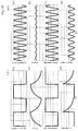
- Diagram showing the intensity of light emitted from the material during the excitation period Diagram showing the decay curve of the emission due to the carrier lifetime in the material, A diagram showing the change in intensity of light emitted from a material when the material is excited with a rectangular wave, An explanatory view of a measuring method and measuring apparatus for applying a modulated excitation to a material and modulating and detecting light emitted from the material with a phase opposite to that of the excitation, A diagram showing the modulation of the excitation applied to the material, the modulation of the light emitted from the material and the intensity change of the separated attenuated light when using the measuring device shown in FIG.
- Diagram showing the relationship between the ratio of detection light obtained at different frequencies and the carrier life
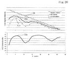
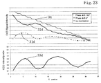
- a diagram showing the characteristics of the material used in the simulation, in which the light emission intensity and the carrier lifetime fluctuate at each position of the X coordinate, Indicates the modulation of excitation applied to the material, the modulation of light emitted from the material, and the change in intensity of the separated attenuated light when switching the modulation frequency of excitation applied to the material and the modulation frequency of light emitted from the material Diagram, The variation characteristics in the X coordinate of the intensity of detection light obtained by modulation of each frequency shown in FIG.
- Diagram 10 and the variation characteristic in the X coordinate of the ratio of detection output obtained by modulation of different frequencies are compared Diagram, A diagram showing the intensity of detection light detected continuously from the material when the material is subjected to continuous excitation, A diagram showing a change in intensity of light emitted from a material and a change in intensity of separated attenuated light when the modulation on the excitation side and the modulation on the light reception side are trapezoidal waveforms.
- Line diagram A diagram showing the relationship between the carrier lifetime and the ratio of detection light obtained by modulation of a trigonometric function waveform and at different frequencies.
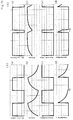
- a diagram showing the relationship between the ratio of detection light obtained by modulation of different phase differences and the carrier life A diagram showing a change in intensity of light emitted from a material and a change in intensity of separated attenuated light when modulation is performed with waveforms having different duty ratios.
- the present invention evaluates a material by detecting light (luminescence) emitted from the material such as a semiconductor.
- various levels such as a conduction band or a non-emitting center, an impurity level, a defect induced level, and the like based on the energy of electrons exist.
- carrier lifetime occurs in the process of recombining with holes and disappearing with a certain probability.
- the energy of the excited electrons is converted to light, and it is converted to lattice vibration and transmitted to the material as heat.
- the light emission characteristics at this time reflect the electronic structure unique to the crystal and various defects.
- the carrier life becomes short. Therefore, it is important to measure the carrier lifetime in order to know the defect status and purity of the material.
- Crystals for solar cells need to have fewer defects.
- defect density is high, excited electrons (electrical energy) generated by irradiation of sunlight are captured by defect levels and converted to heat or re-emitted, and can not be extracted as electrical energy.
- power generation occurs when carriers generated in the light receiving section of the solar cell reach the electrodes, but power generation can not be performed if the electrodes do not exist within the diffusion distance derived from the carrier life. Therefore, if the carrier lifetime is long, the electrode arrangement density can be reduced and the light receiving area can be increased.
- the solar cell characteristics are successively determined in the process of manufacturing or processing the light receiving part (power generation part) itself and the inspection process in each process. I can know. For example, it is necessary to form a pn junction to be a light receiving part with high quality, but for a manufacturing process that can not be reprocessed, such as ion implantation / annealing or growth of conductive crystals, the carrier life is By measuring, the quality as a solar cell can be evaluated before the whole process is completed.
- the measuring method and measuring apparatus of the present invention measure luminescent light (emission of light from a material) in a noncontact manner to determine the carrier lifetime of the material at high speed and at low cost. Therefore, it is characterized in that the light emission during excitation and the light emission after excitation are measured separately or separately. Furthermore, it is characterized in that the light emission repeatedly separated is accumulated and recorded.
- the carrier lifetime is evaluated by photoluminescence.
- Photoluminescence is a concept of a process in which excited electrons excited by light emit light when they recombine with holes.
- the excitation and light emission in the present invention are not limited to photoluminescence, and can be implemented by electroluminescence or the like.
- FIG. 1 shows luminescence light when excitation light is applied continuously to a wafer such as silicon (Si) for a predetermined time, and the horizontal axis is time, and the vertical axis is the light emission size.
- the magnitude of the luminescence light by excitation of the continuous light is A CW P.
- a CW is the excitation intensity
- P is the light emission probability (frequency).
- the hatched area in FIG. 1 corresponds to a value A CW PT m obtained by integrating the light emission magnitude with the measurement time, with the time T m as the measurement time.
- FIG. 2 shows the relationship between light emission and carrier lifetime when excitation light is given to a semiconductor material such as silicon, the horizontal axis is time, and the vertical axis is the light emission size.
- the probability distribution of the emission becomes an exponential decay curve.
- the excitation light is a delta function of the amplitude A ⁇
- the decay curve of the light emission probability is expressed by APe ⁇ t / ⁇ (e is a natural number).
- the above ⁇ is a parameter of carrier lifetime. That is, the time ⁇ required for the initial light emission to decrease to 1 / e can be evaluated as a carrier lifetime parameter.
- FIG. 3 shows the relationship between the magnitude of light emission from a material and time when a steep pulse of excitation light is given to the material.
- the change in the magnitude of light emission is indicated by a thick solid line.
- the magnitude of the light emission shows a characteristic that rises in a curve as time passes, and after the fall of the excitation light, the intensity of light emission decays in a curve like time Show the characteristics.
- the area of the hatched region in FIG. 3 is a integrated integration value of the emission magnitude at time time width T P of the excitation light pulse, the amplitude and A P, the integral value of the light emission and PT P A P become.
- the light emission at this time is a state in which the light emission probability (frequency) P and the carrier life are mixed without being distinguishable from each other, and the integral value is not the one in which only the information of the carrier life is extracted.
- the decay curve of the light emission after the fall of the pulse of the excitation light has the convolution characteristic of APe ⁇ t / ⁇ shown in FIG. 2 and includes the parameter ⁇ of the carrier lifetime.
- the present invention is intended to evaluate the carrier life by separately acquiring the attenuated light which attenuates following the falling of the excitation pulse in FIG.
- the decay time of the light emission after the fall of the pulse is extremely short, it is necessary to have a light receiving device that responds extremely fast in order to acquire only the separated attenuated light.
- the attenuating light is weak, in order to obtain the attenuating light, it is necessary to repeatedly acquire the attenuating light many times using a light receiving device that responds at high speed, and the light receiving is extremely advanced. Technology is required.
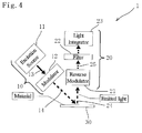
- FIG. 4 illustrates a measurement method and a measurement apparatus of a basic embodiment of the present invention capable of providing excitation to a material, separating attenuation light from light emitted from the material, and acquiring a plurality of separated attenuation lights. Is shown.
- the measuring device 1 shown in FIG. 4 has an excitation device 10 and a detection device 20.
- the excitation device 10 has an excitation source 11 and a modulation device 12 on the excitation side.
- the detection device 20 has a modulation device 21 on the light reception side, a filter 22 and a light reception device 23.
- the excitation source 11 is a continuous oscillation type semiconductor laser, and the modulation device 12 on the excitation side and the modulation device 21 on the light reception side are acousto-optic elements.
- the light receiving device 23 is an integral type light receiving device that accumulates and detects light in a predetermined exposure time, and is, for example, a light receiving device having a large number of CCD elements.
- the filter 22 is a wavelength filter or a polarization filter.
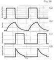
- FIG. 5A shows the waveform of the excitation light 14 after the continuous light 13 emitted continuously from the excitation source 11 is modulated by the modulation device 12 on the example side.
- the acousto-optical element used as the modulation device 12 controls the lattice constant at the ultrasonic frequency to switch the refractive index for the passing continuous light 13 at high speed. Therefore, as shown in FIG. 5A, the magnitude of the excitation light 14 that has passed through the modulation device 12 can be modulated so that the rise and fall are substantially close to rectangular waves.
- the duty ratio between the irradiation (excitation) of the excitation light 14 and the period shown in FIG. 5A is 50%.
- FIG. 5 (b) shows the intensity change of the luminescence light 24 emitted from the semiconductor material 30 when the excitation light 14 is given to the semiconductor material 30 such as silicon.
- the size of the luminescence light 24 increases in a curved manner according to time following the sharp rise of the excitation light 14 and follows the steep fall of the excitation light 14. Attenuate.
- FIG. 5C shows a modulation waveform by the modulation device 21 on the light receiving side.
- the modulation waveform rises in synchronization with the falling of the excitation light 14 shown in FIG. 5A and is set to fall in synchronization with the rising of the excitation light 14.
- the modulation device 12 on the excitation side and the modulation device 21 on the light reception side are configured by the same acousto-optic element, and the modulation device 12 on the excitation side and the modulation device 21 on the light reception side operate with control signals of the same frequency and opposite phase to each other Do.
- FIG. 5D shows the separated light 25 after the luminescence light 24 emitted from the semiconductor material 30 is modulated by the modulation device 21 on the light receiving side.
- the luminescence light 24 shown in FIG. 5B the light during the excitation time when the excitation light 14 is irradiated is not acquired by the modulation of the modulation device 21 on the light reception side, and the end of the excitation light 14 (excitation time End) is extracted.
- the modulation at the time of light reception shown in FIG. Luminescent light 24 may be obtained simultaneously with or after the end).
- FIG. 5 (b) shows the intensity change of the luminescence light 24 emitted from one of the regions of the semiconductor material 30, and the split light 25 of FIG. 5 (d) is a region of that one. Attenuation light 26 is separated from luminescence light 24 emitted from the light source.
- the area of one point is one pixel detected by the light receiving device 23, and is positioned as an area where the CCD element, which is one light receiving element, can receive light.
- the separated light 25 shown in FIG. 5D passes through the filter 22 so that the light component including the attenuated light 26 is extracted and received by the light receiving device 23.
- the CCD element provided in the light receiving device 23 has an exposure time for accumulating light after the start of light reception until the detection output is shifted to the memory.
- the modulation period shown in (c) is set sufficiently short. This exposure time is a measurement time for accumulating (integrating) and detecting the plurality of separated lights 25 shown in FIG.
- the attenuated light 26 emitted following the end of the excitation light 14 includes the carrier lifetime parameter ⁇ , and the detection light in which a plurality of attenuated lights 26 are stored is It contains information on carrier life.
- the exposure time of the light receiving device 23 is set by setting the modulation waveform shown in FIGS. 5A and 5C to a relatively high frequency.
- a large number of attenuated lights 26 can be accumulated (integrated) and detected, and as a result, the intensity of the detected light can be taken out as an output of a sufficiently high level compared with the detection noise of the light receiving device 23 and other noises. .
- FIG. 6 shows the relationship between the modulation frequency of the modulation device 12 on the excitation side and the modulation device 21 on the light reception side and the intensity of the detection light accumulated and received by the attenuation light 26 in the CCD element of the light reception device 23.
- the logarithmic axis of the horizontal axis is the modulation frequency
- the vertical axis is the intensity of the detection light.
- the carrier life is stepwise: 50 nsec, 70 nsec, 100 nsec, 150 nsec, 200 nsec, 300 nsec, and 500 nsec. It is the result of simulating the intensity change of detection light supposing the material which changes to.
- the modulation frequency when the modulation frequency is low and the modulation period is sufficiently longer than the time ⁇ which is a parameter of the carrier lifetime, the light amount of the attenuation light 26 accumulated during the exposure time is small and the attenuation light The intensity of the detected light having accumulated 26 becomes almost zero.
- the modulation frequency is increased, the number of attenuation light beams 26 accumulated during the exposure time increases in proportion to the increase, so the intensity of the detection light having accumulated the attenuation light beams 26 increases almost linearly.
- the intensity of the detection light nonlinearly increases as the modulation frequency increases. Furthermore, when the modulation frequency becomes high, the light amount of the attenuated light 26 accumulated in the acquisition time T1 is saturated, and as shown in FIG. 6, the intensity of the detection light is saturated.
- the level at which the intensity of the detection light is 50% of the saturation value is indicated by the horizontal line of the broken line.
- the intensity of the detected light measured for the material of each carrier life changes almost linearly with the logarithmic increase of the modulation frequency It is located in the area where
- the modulation of the excitation light shown in FIG. 5 (a) and the modulation of the light reception shown in FIG. 5 (c) are performed using any single modulation frequency (measurement frequency)
- the modulation frequency (measurement frequency) at this time it is preferable to use a region where the intensity of the detection light rises approximately linearly with the logarithmic increase of the horizontal axis in FIG.
- the intensity of detection light from each measurement point is acquired In the same material, the intensity of detection light is high in places where the carrier life is long, and the intensity of detection light is low in places where the carrier life is short, and the intensity of detection light from the material corresponds to the intensity of the light It becomes possible to grasp as data.
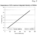
- the diagram shown in FIG. 7 is one in which the proportional relationship between the nominal carrier life and the modulation frequency in FIGS. 5 (a) and 5 (c) is obtained based on the simulation shown in FIG.
- the horizontal axis represents the nominal carrier lifetime
- the vertical axis represents 1 / modulation frequency, that is, the modulation period.
- the straight line in the solid line in FIG. 7 corresponds to the line connecting the intersections of the characteristic curve (solid line) of the material of each carrier life shown in FIG. 6 and the broken line. That is, the solid line in the diagram of FIG. 7 shows the relationship between the modulation period when the intensity of the detection light is 50% of the saturation value and the nominal carrier life of the material.
- the modulation period (modulation frequency) when the intensity of the detection light becomes 50% of the saturation value changes in proportion to the carrier life, and the proportional constant K is 0.13.
- the proportional relationship shown in FIG. 7 is not necessarily limited to the carrier lifetime in the range of 50 nsec to 500 nsec.
- the modulation frequency as a guideline for the carrier life described above does not necessarily have to be 50% of the saturation value, and in the region where the intensity of the detection light linearly changes with respect to the modulation frequency, the intensity of the detection light
- the carrier lifetime may be determined from the frequency when the value of the signal reaches 60% or 40% of the saturation value, for example.
- the change in the intensity of the detection light obtained when the material is excited includes both the intensity component attributed to the light emission intensity (emission probability) A CW P of the material and the intensity component of the carrier life.
- a CW P of the material the intensity component of the carrier life.
- FIGS. 5 and 6 by sweeping the modulation frequency, it is possible to quantitatively and accurately determine the carrier lifetime.
- the detection light having accumulated (integrated) the attenuated light 26 is measured using two fixed modulation frequencies thereafter, and different modulations are performed.
- the ratio of the intensities of the two detection lights obtained at the frequency it is possible to offset the emission intensity (emission probability) and extract the intensity component of the carrier life as an absolute measurement value.
- This measurement method makes it possible to quantitatively determine the carrier lifetime at high speed without constantly sweeping the modulation frequency.
- this measurement method will be described.
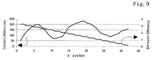
- FIGS. 9 to 11 show simulation results of a measurement method in which information on carrier lifetime is independently extracted from each of the material locations, assuming that the light emission intensity (emission probability) and carrier lifetime vary depending on the location of the material. It shows.
- the horizontal axis in FIG. 9 indicates the coordinate position in the X direction of the material. This material gradually decreases as the light emission intensity (emission probability) goes to the right of the X coordinate, and the carrier life increases and decreases in a wavelike manner as the X coordinate changes.
- FIG. 10A shows the modulation characteristics of the modulator 12 on the excitation side and the modulator 21 on the light reception side in opposite phase with each other in a region of one point on the X coordinate of the material shown in FIG. And the waveform when the modulation frequency is 1 MHz is shown.
- the kind of waveform in FIG. 10A is the same as that in FIG. 5, where (a) is the modulation waveform on the excitation side, (b) is the intensity waveform of the luminescence light emitted from the material, and (c) is the modulation waveform on the light reception side. , (D) are separated waveforms in which the attenuated light is separated.
- the intensity of the detection light can be obtained by integrating the separated light separated in (d) of FIG. 10A for the measurement time corresponding to the exposure time of the CCD element.
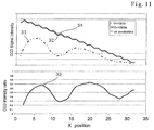
- the intensity of detection light when the modulation frequency is 1 MHz is obtained at a plurality of points on the X coordinate, and a change curve 31 connecting the points is indicated by a two-dot chain line.
- FIG. 10 (B) shows waveforms when the modulation characteristics of the modulator 12 on the excitation side and the modulator 21 on the light reception side are opposite in phase and the modulation frequency is 10 MHz
- FIG. 10 (A) Similarly, (a) is the modulation waveform on the excitation side, (b) is the intensity waveform of the luminescence light emitted from the material, (c) is the modulation waveform on the light receiving side, and (d) is the separated waveform from which the attenuating light is separated. It is.
- the intensity of the detection light at the modulation frequency of 10 MHz is obtained by integrating the attenuated light separated in (d) of FIG. 10B at the same measurement time as at 1 MHz.
- the intensity of detection light when the modulation frequency is 10 MHz is determined at a plurality of points on the X coordinate, and a line 32 connecting the intensities is indicated by a solid line.
- the ratio of the change curve 31 connecting the intensities of the detection light when the modulation frequency is 1 MHz to the line 32 connecting the intensities of the detection light when the modulation frequency is 10 MHz is determined, and this ratio is connected
- the line is shown by the solid curve 33 (1 MHz / 10 MHz). It can be understood that the fluctuation characteristic of the curve 33 is very similar to the fluctuation curve of the carrier life shown in FIG. 9, and that the ratio is based on the information obtained by extracting the carrier life alone.
- the ratio of detection light obtained at two modulation frequencies and the nominal carrier life are approximately linearly proportional. Therefore, it can be understood that the carrier life can be grasped as a quantitative value proportional to the increase or decrease by determining the ratio of the intensities of detection light obtained at different modulation frequencies. This means that even if the light emission intensity (emission probability) A CW P of the material is different and the saturation value of the intensity of the detection light shown in FIG. Means that it can be extracted by
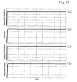
- FIG. 12 shows an example in which continuous excitation light is given to the material without modulating the excitation light as shown in (a). At this time, as shown in (b), continuous luminescence light is obtained from the material, and as shown in (c), the light emission from the material is not modulated. Therefore, as shown in (d) Continuous luminescence light is detected.
- the carrier lifetime information can be taken alone also by finding the ratio between the intensity of the detection light obtained by modulating the excitation light and the luminescence light and the intensity of the detection light obtained by the continuous excitation light. Can.
- the modulation characteristics of light by the modulator 12 on the excitation side and the modulator 21 on the light reception side follow a rectangular wave that rises sharply and falls sharply, and with the modulation device 12 on the excitation side
- the modulation characteristics may not be accurate rectangular wave characteristics due to the influence of the ability of the modulation device or noise, etc., and between the modulation operation of the modulation device 12 on the excitation side and the modulation operation of the modulation device 21 on the light reception side. Time lag may occur.
- the measurement method and the measurement apparatus according to the present invention can exhibit the characteristics even if the modulation characteristic is not a rectangular wave with accuracy and the modulation on the excitation side and the modulation on the light reception side are temporally shifted. It is possible to retrieve information on carrier life alone.
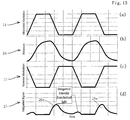
- the modulation characteristic by the modulator 12 on the excitation side shown in (a) is a trapezoidal waveform. Therefore, the luminescent light 24 having the characteristics shown in (b) is emitted from the material.
- the modulation characteristic of the light receiving side modulation device 21 shown in (c) is also a trapezoidal waveform.
- the modulation of the trapezoidal waveform on the excitation side shown in (a) and the modulation of the trapezoidal waveform on the light receiving side shown in (c) are in antiphase with each other and are synchronized with each other at the same frequency.
- the separated light 25 shown in (d) is detected by the light receiving device 23.
- the modulation characteristic on the light receiving side shown in (c) is a trapezoidal waveform, in the light component 26a obtained by the separated light 25 shown in (d), not only the attenuated light emitted following the excitation time but also the excitation light Some of the components of the light emitted are also included.
- the intensity of detection light obtained by the modulation waveform shown in FIG. 13 was determined by simulation.
- the intensity of detection light is obtained by integrating separated light 25 obtained at each location of the X coordinate in measurement time corresponding to the exposure time of the CCD element.
- the change curve 31a is indicated by a two-dot chain line in FIG.
- the modulation frequency shown in FIGS. 13 (a) and 13 (c) is 10 MHz
- the intensity of the detection light is obtained by integrating the separated light 25 obtained from each of the X coordinates in the measurement time.
- the line 32a connecting the strengths is indicated by a solid line.
- a curve 33a is obtained by determining the ratio between the intensity of detection light obtained when the modulation frequency is 1 MHz and the intensity of detection light obtained when the modulation frequency is 10 MHz.
- This curve 33a closely approximates the characteristics of the increase and decrease of the carrier life shown in FIG. That is, also by obtaining the ratio of the intensities of the detection light obtained at different modulation frequencies based on the modulation characteristics shown in FIG. 13, it is possible to obtain information in which the carrier lifetime is independently extracted.
- FIG. 15 shows the ratio of the intensity of the detection light determined at the modulation frequency of 1 MHz to the intensity of the detection light determined at the modulation frequency of 10 MHz in the modulation characteristics shown in FIG. It is shown in relation to carrier life.
- FIG. 15 shows the same evaluation as that of FIG. As shown in FIG. 15, the ratio changes almost linearly with respect to the nominal carrier life, and based on the modulation characteristics shown in FIG. 13, the ratio of the intensity of detection light obtained at different modulation frequencies is determined. It can be seen that this ratio corresponds in proportion to the length of the carrier life.
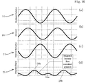
- the modulation characteristic on the excitation side shown in (a) has a waveform approximating a triangular function, and the material emits luminescence light 24 having the characteristic shown in (b).
- the modulation characteristic on the light receiving side shown in (c) is also a waveform approximated to a trigonometric function.
- the modulation of the trigonometric function waveform on the excitation side shown in (a) and the modulation of the trigonometric function waveform on the light receiving side shown in (c) are synchronized so as to be in antiphase with each other at the same frequency.
- the intensity change of the separated light 25 obtained by modulating the luminescent light 24 emitted from the material is shown.
- the luminescence light 24 having the characteristics shown in (b) receives modulation of the trigonometric function waveform shown in (c)
- the light component 26b included in the separated light 25 shown in (d) is attenuated after the excitation time Only the light component is included, and a part of the light component emitted at the excitation time is also included.
- FIG. 17 shows the change curve 31b of the intensity of the detection light obtained at the modulation frequency of 1 MHz with the trigonometric function waveform shown in FIG. 16 and the fluctuation of the intensity of the detection light obtained with the modulation frequency of 10 MHz with the trigonometric function waveform.
- a line 32b is shown, and a curve 33b is shown in which the ratio between the change curve 31b and the line 32b is obtained.
- This curve 33 b is similar to the fluctuation curve of the carrier life of the material shown in FIG. 9, and it is understood that the information on the carrier life is extracted.
- a characteristic equivalent to that of the curve 33b can also be obtained from the ratio of the change curve 31b shown in FIG. 17 to the line 34 showing a change of 1 ⁇ 4 of the intensity of luminescence light obtained by continuous excitation light.
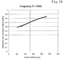
- FIG. 18 corresponds to FIG. 15, and the intensity of detection light obtained at a modulation frequency of 1 MHz in the trigonometric function waveform shown in FIG. 16 and the intensity of detection light obtained at a modulation frequency of 10 MHz in the trigonometric function waveform And the relationship between the ratio and the nominal carrier life. It is possible to obtain information proportional to the component of the carrier life by obtaining the ratio of the intensity of the detection light obtained at different frequencies even when modulated by the trigonometric function waveform from FIG.
- the measurement method of removing the component of the emission intensity and quantifying the carrier lifetime component is the ratio of the intensity of the detection light at different modulation frequencies as described above, and 1/4 of the intensity of the detection light by the continuous light. In addition to using the value of, it is also possible to use the following measurement method.
- the simulation shown in FIG. 19 shows that it is possible to extract information on the carrier life alone by assuming the material having the characteristics shown in FIG. 9 and finding the ratio of the intensity of detection light obtained when the modulation waveform is made different. ing.
- FIG. 19 (A) is the same as the waveform of FIG. 10 (A), the modulation waveform on the excitation side shown in (a) is a rectangular wave, and the modulation waveform on the light receiving side shown in (c) is also a rectangular wave .
- the modulation waveform on the excitation side shown in (a) and the modulation waveform on the light reception side shown in (c) are synchronized such that their phases are opposite to each other at the same frequency of 1 MHz.
- It is the intensity of the detection light that the separated light obtained in (d) is integrated at a measurement time corresponding to the exposure time of the CCD.
- the distribution on the X coordinate of the intensity of the detection light obtained by the modulation of the rectangular wave is shown by a change curve 31c of a two-dot chain line.
- FIG. 19 (B) is the same waveform as FIG. 16, and is a curve in which the modulation waveform on the excitation side shown in (a) and the modulation waveform on the light receiving side shown in (c) approximate to a trigonometric function.
- the modulation waveform of (a) and the modulation waveform of (c) have the same frequency, and are in antiphase with the phase shifted by 180 degrees.
- the rectangular waves shown in (a) and (c) of FIG. 19A and the trigonometric function waveforms shown in (a) and (c) of FIG. 19B have the same frequency of 1 MHz.
- FIG. 20 the distribution on the X coordinate of the intensity of the detection light obtained by the modulation of the trigonometric function waveform is shown by a change curve 32c of a solid line.
- FIG. 20 shows a curve 33c obtained by determining the ratio between the change curve 31c of the intensity of the detection light obtained by the modulation of the rectangular wave and the change curve 32c of the intensity of the detection light obtained by the modulation of the trigonometric function waveform. It is done.
- the curve 33c approximates the fluctuation curve of the carrier life shown in FIG. 9, and it can be seen that the information on the carrier life is reflected.
- FIG. 21 shows the relationship between the ratio of (intensity of detection light by modulation of rectangular wave) / (intensity of detection light by modulation of trigonometric function waveform) and the nominal carrier life. From FIG. 21, the magnitude of the ratio of the intensity of the detection light obtained by the modulation of the rectangular wave and the intensity of the detection light obtained by the modulation of the trigonometric function waveform substantially follows the change of the size of the carrier life Can understand.
- the simulation shown in FIG. 22 assumes materials of the characteristics shown in FIG. 9, and the intensities of two types of detection light obtained by making the phase difference between the modulation waveform on the excitation side and the modulation waveform on the light reception side different.
- the determination of the ratio indicates that information on carrier lifetime can be extracted alone.
- the waveforms shown in FIG. 22 (A) are the same as in FIGS. 10 (A) and 19 (A), and the modulation waveform on the excitation side shown in (a) and the modulation waveform on the light receiving side shown in (c) are It is a rectangular wave with a phase difference of 180 degrees at the same frequency of 1 MHz.
- the intensity of the detection light is obtained by integrating the separated light obtained in (d) at a measurement time corresponding to the exposure time of the CCD.
- the distribution of the intensity of the detection light on the X coordinate is It is shown by a change curve 31d of a two-dot chain line.
- the modulation waveform on the excitation side shown in (a) and the modulation waveform on the light reception side shown in (c) are rectangular waves, and the phase difference between the excitation side and the light reception side is 0 degrees.
- the duty ratios of the rectangular wave shown in (a) and (c) of FIG. 22 (A) and the rectangular wave shown in (a) and (c) of FIG. 22 (B) are both 50% and the frequency is 1 MHz.
- a line 32d indicating the distribution on the X coordinate of the intensity of the detection light obtained by the modulation of FIG. 22 (B) is indicated by a solid line.
- FIG. 24 shows a relationship between a ratio of (intensity of detection light by modulation of FIG. 22A) / (intensity of detection light by modulation of FIG. 22B) and a nominal carrier life. It is possible to obtain information proportional to the component of the carrier life by obtaining the ratio of the intensities of the two types of detection light modulated by rectangular waves of different phase differences from FIG.
- the simulation shown in FIGS. 25 to 27 relates to the carrier life by assuming the material having the characteristics shown in FIG. 9 and determining the ratio of the intensities of two types of detection light obtained by making the duty ratio of the modulation waveform different. It indicates that information can be extracted independently.
- the waveforms shown in FIG. 25 (A) are the same as those in FIGS. 10 (A), 19 (A) and 21 (A), and the modulation waveform on the excitation side shown in (a) and the light reception shown in (c)
- the modulation waveform on the side is a rectangular wave whose phase is opposite to each other at the same frequency of 1 MHz.
- the modulation waveform on the excitation side shown in (a) and the modulation waveform on the light receiving side shown in (c) are rectangular waves in reverse phase at a frequency of 1 MHz.
- FIG. 25 (A) shows that the duty ratio of the modulation waveform is 50:50
- FIG. 25 (B) shows that the duty ratio is 90:10.
- a change curve 31f showing the distribution on the X coordinate of the intensity of the detection light obtained by the modulation of FIG. 25A is shown by a two-dot chain line, and obtained by the modulation of FIG.
- a change curve 32f showing the distribution of the intensity of the detected light on the X coordinate is shown by a solid line.
- a curve 33f is shown in which the ratio between the change curve 31f and the change curve 32f is obtained. This curve 33 f is similar to the fluctuation curve of the carrier life shown in FIG. 9, and it can be seen that the information of the carrier life is reflected.
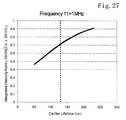
- FIG. 27 shows the relationship between the ratio of (intensity of detection light by modulation of FIG. 25A) / (intensity of detection light by modulation of FIG. 25B) and the nominal carrier life. It can be understood from FIGS. 26 and 27 that the information on the carrier life can be extracted from the ratio of the intensities of the detection light measured with different duty ratios.
- the ratio of the intensities of two types of detection light obtained by modulation of different frequencies is determined.
- the ratio of the intensity of detection light obtained by intermittent excitation to the intensity of detection light obtained by continuous excitation is determined.
- the modulation on the excitation side or the modulation on the light reception side is performed with a waveform other than a rectangular wave.
- the ratio of the intensities of the two types of detection light obtained by modulation whose waveforms are different from each other is determined.
- the ratio of the intensities of the two types of detection light obtained by making the phase difference between the modulation on the excitation side and the modulation on the light reception side different from each other is determined.
- the ratio of the intensities of the two types of detection light obtained by modulation of different duty ratios is determined.
- the above conditions can be combined with one another.
- the intensity of the detection light obtained by the modulation of a rectangular wave of, for example, 1 MHz shown in FIG. 28A and the waveform approximated to the trigonometric function shown in FIG. It is also possible to independently extract information on the carrier lifetime by determining the ratio of the intensities of detection light obtained by 10 MHz modulation.
- the modulation on the excitation side shown in (a) and the modulation on the light receiving side shown in (c) both have a 50% duty ratio and opposite-phase rectangular waves In this way, the attenuated light following the end of the excitation time, which excites the material, is separated from the light during excitation.
- the modulation on the excitation side shown in (a) and the modulation on the light reception side shown in (c) are both based on a rectangular wave with a duty ratio of 40%. Of the light modulation and the light modulation on the light receiving side are 144 degrees out of phase.
- This configuration also allows the attenuated light to be separated from the light being excited in synchronization with the end of the excitation time when the material is excited.
- the modulation on the excitation side and the modulation on the light reception side are not limited to the phase difference of 180 ° and the duty ratio of 50%, and any modulation waveform that can separate the attenuation characteristics may be used.
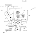
- FIG. 30 shows a measuring device 40 suitable for implementing the measuring method described above.
- the excitation device 10 has an excitation source 11 and a modulation device 12 on the excitation side.
- the excitation source 11 is a continuous emission semiconductor laser
- the modulation device 12 is an acousto-optic element.
- the continuous light 13 emitted from the excitation source 11 is modulated by the modulation device 12 to become excitation light 14.
- a lens 41 is provided in front of the modulation device 12, and the modulated excitation light 14 is optically modulated to be applied to a predetermined area of the surface of the material 30.
- the lens 41 is a collimating lens, a convex lens or a concave lens having a large focal ratio, or a combination thereof, and is configured such that the difference in the amount of light given to the area of the predetermined area of the material 30 is minimized.
- the detection device 20 includes a modulation device 21 and a light reception device 23 on the light reception side.
- the modulation device 21 is an acousto-optic element.
- a condenser lens 42 is provided between the material 30 and the modulator 21.
- the luminescence light 24 emitted from a predetermined region of the material 30 is condensed by the condenser lens 42 and supplied to the modulator 21, and the separated light 25 separated by the modulator 21 is received by the light receiver 23.
- the light receiving device 23 is a light receiving element array in which a plurality of CCD elements are arranged, and in front of it, a camera lens 43 for condensing the separated light 25 on the light receiving element array is provided.
- the detection device 20 is equipped with the filter 22 shown in FIG. 4 as necessary.
- the luminescence light 24 emitted from the area of the predetermined area of the material 30 is converted into individual CCDs.
- the element can simultaneously receive light.
- the intensity of the detection light obtained by each CCD element can provide information on the carrier life of each point in the area of a fixed area. Also, by calculating the ratio as shown by the curve 33 in FIG. 11 with respect to the intensity of the detection light detected by each CCD element, information on the carrier life is extracted for each point in a wide area. It is possible.
- the direction in which the table on which the material 30 is installed is orthogonal to the line
- the transfer device 45 for moving the light intermittently or continuously, it is possible to sequentially obtain luminescence light from a wide area of the material 30 by the CCD element of the light receiving device 23. This is the same even if the table on which the material 30 is installed is fixed and the measuring device 40 moves.
- the measurement apparatus 40 shown in FIG. 30 has a modulation control unit 46.
- the modulation control unit 46 controls the modulation device 12 on the excitation side and the modulation device 21 on the light reception side, and modulation of excitation light and modulation of luminescence light are performed as shown in each drawing.
- the measuring device 40 is provided with a determination unit 47 that also functions as a main control unit, and controls the excitation source 11 and the modulation devices 12 and 21. At the same time, detection light obtained by accumulating the individual CCD elements of the light receiving device 23 during the exposure time is stored in the memory, converted into a digital value, and supplied to the determination unit 47. In the discrimination section 47, calculation of the ratio as shown by the curve 33 in FIG. 11 is performed, and it is possible to obtain information of carrier life of each point of the measurement area of the material 30 with each CCD element as a pixel unit.
- the information on the carrier life of each point of the material 30 calculated by the determination unit 47 can be used as comparison information in the area of a predetermined area.
- the carrier life of each point can be displayed as numerical information on the display device, or can be displayed as an illustration image having gradation corresponding to the carrier information.
- each CCD is a pixel unit of gradation.
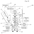
- the measuring apparatus 40A shown in FIG. 31 is provided with a beam splitter 51 for separating the luminescent light 24 emitted from the material 30, and a component of the luminescent light 24 directed to the condensing lens 42 and a component directed to the second camera lens 52. Separated into Then, the light passing through the second camera lens 52 is given to the second light receiving device 53 without passing through the modulation device. In this measuring device 40A, detection light obtained by modulating the luminescence light 24 and detection light without modulation can be obtained by one measurement.
- the light separated by the beam splitter 51 may be modulated by the second modulator and detected by the light receiver 53. Thereby, detection light of different modulation can be obtained by one measurement.
- the present invention is not limited to the above embodiment, and various modifications are possible.
- excitation light 14 modulated to various duty ratios can be obtained without providing the modulation device 12.
- the light receiving device 23 is used so that each detection element can intermittently receive light and the detection output intermittently received can be stored in the memory, the luminescence light can be obtained without providing the modulation device 21. It is possible to separate the attenuated light, which is a component of the carrier lifetime, and to accumulate the separated attenuated light at a predetermined exposure time.
- the excitation device 10 does not emit excitation light, but generates intermittent power, and the carrier lifetime is measured by electroluminescence in which carriers in the material 30 are excited by this power and recombined to emit light. It is also possible.
- materials to be measured by the measuring method and measuring apparatus of the present invention include silicon (Si), indium phosphide (InP), silicon carbide (SiC), gallium arsenide (GaAs), silicon germanium alloy (SiGe), germanium
- Typical semiconductor crystal materials are (Ge), chalcopyrite-type compounds (CuInS2), chalcopyrite-based polycrystalline films (Cu (In, Ga) Se2), fullerene (C60) derivative-based organic semiconductors, etc.
- Other semiconductor materials may be used.
- organic materials, polymer materials, and the like as long as they emit light when the internal carriers are excited and activated by the excitation light and the excitation power and the energy level of the carriers such as electrons decreases. It is also good.
Landscapes
- Health & Medical Sciences (AREA)
- Nuclear Medicine, Radiotherapy & Molecular Imaging (AREA)
- Physics & Mathematics (AREA)
- Life Sciences & Earth Sciences (AREA)
- Chemical & Material Sciences (AREA)
- Analytical Chemistry (AREA)
- Biochemistry (AREA)
- General Health & Medical Sciences (AREA)
- General Physics & Mathematics (AREA)
- Immunology (AREA)
- Pathology (AREA)
- Investigating, Analyzing Materials By Fluorescence Or Luminescence (AREA)
- Testing Or Measuring Of Semiconductors Or The Like (AREA)
Abstract
Description
励起時間が間隔を空けて繰り返されるように、材料に励起を与え、
複数の励起時間を含む長さの測定時間内に、材料から励起時間に発せられる光と励起時間の終末に続いて発せられる減衰光とを分離し、
前記測定時間内に、分離された複数の前記減衰光を蓄積して検知し、蓄積された検知光の強度に基づいてキャリアの寿命を測定することを特徴とするものである。
励起時間が間隔を空けて繰り返される励起を材料に与える励起装置と、
複数の励起時間を含む長さの測定時間内に、材料から励起時間に発せられる光と励起時間の終末に続いて発せられる減衰光とを分離し、前記測定時間内に、分離された複数の前記減衰光を蓄積して検知する検知装置と、を有することを特徴とするものである。
異なる周波数で励起したときに前記検知装置で取得される検知光の強度の比から、発光強度の成分を除去し、キャリアの寿命成分を定量化して測定する判別部が設けられているものとして構成できる。
励起時間が間隔を空けて繰り返されるように材料に励起を与えたときに前記検知装置で取得される検知光の強度と、前記検知装置で材料から発せられる光を連続して検出した検出光の強度との比から、発光強度の成分を除去し、キャリアの寿命成分を定量化して測定する判別部が設けられているものとして構成できる。
異なる波形の変調で得られた検知強度の比から、発光強度の成分を除去し、キャリアの寿命成分を定量化して測定する判別部が設けられているものとして構成できる。
異なる位相の変調で得られた検知強度の比から、発光強度の成分を除去し、キャリアの寿命成分を定量化して測定する判別部が設けられているものとして構成できる。
異なるデューティ比のときに減衰光が蓄積されて得られた検知光の強度の比から、発光強度の成分を除去し、キャリアの寿命成分を定量化して測定する判別部が設けられているものとして構成できる。
(1)異なる周波数の変調で得られた2種類の検知光の強度の比を求める。
(2)間欠的な励起により得られた検知光の強度と、連続する励起により得られた検知光の強度との比を求める。
(3)矩形波以外の波形で励起側の変調または受光側の変調を行う。
(4)互いに波形が相違する変調で得た2種類の検知光の強度の比を求める。
(5)励起側の変調と受光側の変調との位相差を互いに相違させて得た2種類の検知光の強度の比を求める。
(6)異なるデューティ比の変調で得られた2種類の検知光の強度の比を求める。
例えば、図28(A)に示す例えば1MHzの矩形波の変調で得られた検知光の強度と、図28(B)に示す三角関数に近似した波形であって矩形波よりも周波数が高い例えば10MHzの変調で得られた検知光の強度の比を求めることによっても、キャリア寿命に関する情報を独立させて抽出することが可能である。
例えば、励起源11として間欠的に発光するパルス発光レーザを使用すると、変調装置12を設けなくても、種々のデューティ比に変調した励起光14を得ることができる。また、受光装置23を、それぞれの検知素子が光を間欠的に受光し、間欠的に受光した検知出力をメモリに蓄積できるものを使用すれば、変調装置21を設けなくても、ルミネッセンス光からキャリア寿命の成分である減衰光を分離し、さらに分離した減衰光を所定の露光時間に蓄積することが可能である。
10 励起装置
11 励起源
12 変調装置
13 連続光
14 励起光
20 検知装置
21 変調装置
22 フィルタ
23 受光装置
24 ルミネッセンス光
25 分離光
26 減衰光
30 半導体材料
40 測定装置
41 レンズ
42 集光レンズ
43 カメラレンズ
45 移送装置
46 変調制御部
47 判別部
51 ビームスプリッタ
52 カメラレンズ
53 受光装置
Claims (36)
- 材料に励起を与え、材料から発せられる光を検知する測定方法において、
励起時間が間隔を空けて繰り返されるように、材料に励起を与え、
複数の励起時間を含む長さの測定時間内に、材料から励起時間に発せられる光と励起時間の終末に続いて発せられる減衰光とを分離し、
前記測定時間内に、分離された複数の前記減衰光を蓄積して検知し、蓄積された検知光の強度に基づいてキャリアの寿命を測定することを特徴とするキャリア寿命の測定方法。 - 材料から発せられる光を励起時間の終末と同時またはそれ以後に取得することで、励起時間に発せられる光から減衰光を分離する請求項1記載のキャリア寿命の測定方法。
- 材料から発せられる光を励起時間の途中から取得することで、励起時間に発せられる光と、前記光の一部および減衰光とを分離する請求項1記載のキャリア寿命の測定方法。
- 励起源から発せられる励起を励起側の変調装置に通過させて、励起時間が間隔を空けて繰り返されるように、材料に励起を与える請求項1ないし3のいずれかに記載のキャリア寿命の測定方法。
- 励起源から励起を断続的に発生させて、励起時間が間隔を空けて繰り返されるように、材料に励起を与える請求項1ないし3のいずれかに記載のキャリア寿命の測定方法。
- 材料から発せられる光を受光側の変調装置に通過させて、励起時間に発せられる光から減衰光を分離し、測定時間に相当する露光時間を有する受光装置によって、複数の減衰光を蓄積して検知する請求項1ないし5のいずれかに記載のキャリア寿命の測定方法。
- 材料から発せられる光を間欠的に受光できる受光装置を用いて、励起時間に発せられる光から減衰光を分離するとともに、測定時間内に複数の減衰光を蓄積して検知する請求項1ないし5のいずれかに記載のキャリア寿命の測定方法。
- 前記受光装置は、複数の受光素子が配列したものであり、それぞれの受光素子で複数の減衰光を蓄積して検知する請求項6または7記載のキャリア寿命の測定方法。
- 複数の受光素子が二次元的に配列した受光装置を使用し、材料の一定の面積の領域から発せられた減衰光をそれぞれの受光素子で同時に取得し、前記領域内における位置とキャリア寿命に関する情報を得る請求項8記載のキャリア寿命の測定方法。
- 複数の受光素子が列を成して配列した受光装置を使用し、複数の受光素子によって材料から発せられる減衰光を同時に取得し、この取得ラインを移動させて、材料の一定の面積の領域内における位置とキャリア寿命に関する情報を得る請求項8記載のキャリア寿命の測定方法。
- 材料に複数の周波数の励起を与え、それぞれの周波数の励起において材料から発せられる減衰光を蓄積した検知光を取得し、異なる周波数の励起で得られた前記検知光の強度の比から、発光強度の成分を除去して、キャリアの寿命成分を定量化して測定する請求項1ないし10のいずれかに記載のキャリア寿命の測定方法。
- 励起時間が間隔を空けて繰り返されるように材料に励起を与えたときに、減衰光が蓄積されて得られた検知光の強度と、材料から発せられる光を連続して検出して得られる検出光の強度との比から、発光強度の成分を除去し、キャリアの寿命成分を定量化して測定する請求項1ないし10のいずれかに記載のキャリア寿命の測定方法。
- 材料に与える励起を異なる波形で変調して、それぞれの変調波形の励起において材料から発せられる減衰光を蓄積した検知光を取得し、異なる波形の変調で得られた検知光の強度の比から、発光強度の成分を除去し、キャリアの寿命成分を定量化して測定する請求項1ないし10のいずれかに記載のキャリア寿命の測定方法。
- 材料から発せられる光を互いに相違する位相の波形で変調して、減衰光を蓄積して検知した検知光を取得し、異なる位相の変調で得られた検知光の強度の比から、発光強度の成分を除去し、キャリアの寿命成分を定量化して測定する請求項1ないし10のいずれかに記載のキャリア寿命の測定方法。
- 材料に励起を与える間隔と励起時間とのデューティ比、および励起時間に発せられる光から減衰光を分離するときの分離時間とこの分離時間の間隔とのデューティ比を相違させ、異なるデューティ比のときに減衰光が蓄積されて得られた検知光の強度の比から、発光強度の成分を除去し、キャリアの寿命成分を定量化して測定する請求項1ないし10のいずれかに記載のキャリア寿命の測定方法。
- 材料に与える励起が励起光である請求項1ないし15のいずれかに記載のキャリア寿命の測定方法。
- 材料に与える励起が励起電力である請求項1ないし15のいずれかに記載のキャリア寿命の測定方法。
- 材料に励起を与え、材料から発せられる光を検知する測定装置において、
励起時間が間隔を空けて繰り返される励起を材料に与える励起装置と、
複数の励起時間を含む長さの測定時間内に、材料から励起時間に発せられる光と励起時間の終末に続いて発せられる減衰光とを分離し、前記測定時間内に、分離された複数の前記減衰光を蓄積して検知する検知装置と、
を有することを特徴とするキャリア寿命の測定装置。 - 前記励起装置が、励起源と、励起源から発せられる励起を、励起時間が間隔を空けて繰り返されるように変調する励起側の変調装置とを有する請求項18記載のキャリア寿命の測定装置。
- 前記励起装置が、励起時間が間隔を空けて繰り返されるように励起を発する励起源を有している請求項18記載のキャリア寿命の測定装置。
- 前記励起源が、発光源である請求項19または20記載のキャリア寿命の測定装置。
- 前記励起源が、励起電力の発生源である請求項19または20記載のキャリア寿命の測定装置。
- 前記検知装置は、前記材料から発せられる光を、励起時間に発せられる光と減衰光とに分離する変調装置と、測定時間に相当する露光時間内に複数の減衰光を蓄積して検知する受光装置とを有する請求項18ないし22のいずれかに記載のキャリア寿命の測定装置。
- 前記検知装置は、材料から発せられる光を間欠的に受光して、励起時間に発せられる光から減衰光を分離するとともに、複数の減衰光を蓄積して検知する受光装置を有する請求項18ないし22のいずれかに記載のキャリア寿命の測定装置。
- 前記検知装置は、材料から発せられる光を励起時間の終末と同時またはそれ以後に取得することで、励起時間に発せられる光から減衰光を分離する請求項23または24記載のキャリア寿命の測定装置。
- 前記検知装置は、材料から発せられる光を励起時間の途中から取得することで、励起時間に発せられる光と、前記光の一部および減衰光とを分離する請求項24記載のキャリア寿命の測定装置。
- 前記受光装置は、複数の受光素子が配列したものであり、それぞれの受光素子が複数の減衰光を蓄積して検知する請求項23ないし26のいずれかに記載のキャリア寿命の測定装置。
- 前記受光装置が、二次元的に配列した複数の受光素子を有しており、それぞれの受光素子で材料の一定の面積の領域から発せられた減衰光が取得されて、前記領域内における位置とキャリア寿命に関する情報が得られる請求項27記載のキャリア寿命の測定装置。
- 前記受光装置が、列を成して配列する複数の受光素子を有し、前記受光装置と材料とを前記列と交叉する向きに相対的に移動させる移送装置を有しており、複数の受光素子によって材料から発せられる減衰光が同時に取得されるとともに、この取得ラインが移動して、一定の面積の領域内における位置とキャリア寿命に関する情報が得られる請求項27記載のキャリア寿命の測定装置。
- 材料と前記検知装置との間に波長フィルタが設けられている請求項18ないし29のいずれかに記載のキャリア寿命の測定装置。
- 材料と前記検知装置との間に偏光フィルタが設けられている請求項18ないし29のいずれかに記載のキャリア寿命の測定装置。
- 材料に与える励起の周波数を変化させる励起装置が設けられ、
異なる周波数で励起したときに前記検知装置で取得される検知光の強度の比から、発光強度の成分を除去し、キャリアの寿命成分を定量化して測定する判別部が設けられている請求項18ないし31のいずれかに記載のキャリア寿命の測定装置。 - 材料に与えられる励起を、励起時間が間隔を空けて繰り返して与える励起装置が設けられ、
励起時間が間隔を空けて繰り返されるように材料に励起を与えたときに前記検知装置で取得される検知光の強度と、前記検知装置で材料から発せられる光を連続して検出した検出光の強度との比から、発光強度の成分を除去し、キャリアの寿命成分を定量化して測定する判別部が設けられている請求項18ないし31のいずれかに記載のキャリア寿命の測定装置。 - 材料に与える励起を異なる波形で変調して、それぞれの変調波形の励起において材料から発せられる減衰光を蓄積して検知する検知装置が設けられ、
異なる波形の変調で得られた検知強度の比から、発光強度の成分を除去し、キャリアの寿命成分を定量化して測定する判別部が設けられている請求項18ないし31のいずれかに記載のキャリア寿命の測定装置。 - 材料から発せられる光を互いに相違する位相の波形で変調して、減衰光を蓄積して検知する検知装置が設けられ、
異なる位相の変調で得られた検知強度の比から、発光強度の成分を除去し、キャリアの寿命成分を定量化して測定する判別部が設けられている請求項18ないし31のいずれかに記載のキャリア寿命の測定装置。 - 材料に励起を与える間隔と励起時間とのデューティ比を相違させる励起装置と、励起時間に発せられる光と減衰光を分離するときの分離時間とこの分離時間の間隔とのデューティ比を相違させる検知装置とを有し、
異なるデューティ比のときに減衰光が蓄積されて得られた検知光の強度の比から、発光強度の成分を除去し、キャリアの寿命成分を定量化して測定する判別部が設けられている請求項18ないし31のいずれかに記載のキャリア寿命の測定装置。
Priority Applications (8)
| Application Number | Priority Date | Filing Date | Title |
|---|---|---|---|
| US13/817,062 US9029801B2 (en) | 2011-02-15 | 2011-02-15 | Apparatus and method for measuring a luminescent decay |
| EP11858857.3A EP2677302B1 (en) | 2011-02-15 | 2011-02-15 | Method and device for measuring carrier lifetime |
| CN201180041790.2A CN103080730B (zh) | 2011-02-15 | 2011-02-15 | 载流子寿命的测定方法以及测定装置 |
| CA2805718A CA2805718C (en) | 2011-02-15 | 2011-02-15 | Apparatus and method for measuring a luminescent decay |
| JP2012557699A JP5843114B2 (ja) | 2011-02-15 | 2011-02-15 | キャリア寿命の測定方法および測定装置 |
| PCT/JP2011/053154 WO2012111093A1 (ja) | 2011-02-15 | 2011-02-15 | キャリア寿命の測定方法および測定装置 |
| KR1020137004053A KR101506101B1 (ko) | 2011-02-15 | 2011-02-15 | 캐리어 수명의 측정 방법 및 측정 장치 |
| TW101104715A TWI567377B (zh) | 2011-02-15 | 2012-02-14 | Method for measuring the life of carrier and measuring device |
Applications Claiming Priority (1)
| Application Number | Priority Date | Filing Date | Title |
|---|---|---|---|
| PCT/JP2011/053154 WO2012111093A1 (ja) | 2011-02-15 | 2011-02-15 | キャリア寿命の測定方法および測定装置 |
Publications (1)
| Publication Number | Publication Date |
|---|---|
| WO2012111093A1 true WO2012111093A1 (ja) | 2012-08-23 |
Family
ID=46672058
Family Applications (1)
| Application Number | Title | Priority Date | Filing Date |
|---|---|---|---|
| PCT/JP2011/053154 Ceased WO2012111093A1 (ja) | 2011-02-15 | 2011-02-15 | キャリア寿命の測定方法および測定装置 |
Country Status (8)
| Country | Link |
|---|---|
| US (1) | US9029801B2 (ja) |
| EP (1) | EP2677302B1 (ja) |
| JP (1) | JP5843114B2 (ja) |
| KR (1) | KR101506101B1 (ja) |
| CN (1) | CN103080730B (ja) |
| CA (1) | CA2805718C (ja) |
| TW (1) | TWI567377B (ja) |
| WO (1) | WO2012111093A1 (ja) |
Cited By (2)
| Publication number | Priority date | Publication date | Assignee | Title |
|---|---|---|---|---|
| WO2017082218A1 (ja) * | 2015-11-09 | 2017-05-18 | 国立研究開発法人理化学研究所 | 光子検出装置、光子検出方法、蛍光相関分光測定装置、蛍光相互相関分光測定装置、動的光散乱測定装置、及び、蛍光顕微鏡 |
| JP2023015045A (ja) * | 2018-04-13 | 2023-01-31 | アプライド マテリアルズ インコーポレイテッド | 光ルミネセンス分光法を用いた有機発光ダイオード製造のための計測学 |
Families Citing this family (13)
| Publication number | Priority date | Publication date | Assignee | Title |
|---|---|---|---|---|
| US9269034B2 (en) * | 2012-08-21 | 2016-02-23 | Empire Technology Development Llc | Orthogonal encoding for tags |
| DE102013109010B4 (de) | 2013-08-21 | 2019-03-14 | Presens - Precision Sensing Gmbh | Verfahren zur Bestimmung einer Veränderlichen einer Probe |
| DE102013112885A1 (de) * | 2013-11-21 | 2015-05-21 | Osram Opto Semiconductors Gmbh | Verfahren zur optischen Charakterisierung eines optoelektronischen Halbleitermaterials und Vorrichtung zur Durchführung des Verfahrens |
| DE102015111213B4 (de) * | 2015-07-10 | 2023-05-04 | Infineon Technologies Ag | Verfahren zum Verringern einer bipolaren Degradation bei einem SiC-Halbleiterbauelement und Halbleiterbauelement |
| CN105629147A (zh) * | 2015-12-28 | 2016-06-01 | 清华大学 | Led载流子寿命测试系统 |
| FR3066590A1 (fr) * | 2017-05-22 | 2018-11-23 | Centre National De La Recherche Scientifique - Cnrs - | Spectroscopie quantitative de densite de defauts electroniques dans un photorecepteur en couches minces, notamment dans une cellule solaire |
| JP7000198B2 (ja) | 2018-02-16 | 2022-01-19 | 浜松ホトニクス株式会社 | キャリア寿命測定方法及びキャリア寿命測定装置 |
| CN110208276B (zh) * | 2019-07-02 | 2023-03-31 | 广州越监工程质量安全检测中心有限公司 | 一种结构砼表观缺陷测定仪及其检测设备 |
| CN110470965B (zh) * | 2019-07-09 | 2020-07-28 | 同济大学 | 一种半导体表面态载流子寿命测试方法 |
| WO2023126910A2 (en) | 2022-01-03 | 2023-07-06 | Einat Ronen | Multi-modal diagnostic device and database service for ophthalmology and neurology |
| KR102704988B1 (ko) * | 2022-02-07 | 2024-09-06 | 한국에너지기술연구원 | 캐리어 수명 측정 장치 및 방법 |
| EP4257958A1 (en) * | 2022-04-05 | 2023-10-11 | Centre national de la recherche scientifique | Method and device for determining the effective electron lifetime in a sample |
| WO2025084986A1 (en) * | 2023-10-17 | 2025-04-24 | National University Of Singapore | Method and system for luminescence characterisation of a semiconductor device |
Citations (7)
| Publication number | Priority date | Publication date | Assignee | Title |
|---|---|---|---|---|
| JPS63312649A (ja) * | 1987-06-16 | 1988-12-21 | Kawasaki Steel Corp | 半導体中の不純物準位およびキャリヤ寿命同時測定方法 |
| JPH0410574B2 (ja) * | 1983-07-08 | 1992-02-25 | ||
| JPH0714893A (ja) * | 1993-06-21 | 1995-01-17 | Sumitomo Metal Mining Co Ltd | 半導体中の多数キャリア寿命の測定方法 |
| JP2006519395A (ja) * | 2003-02-28 | 2006-08-24 | ユーティ―バテル エルエルシー | 集積化チューナブル光センサ(itos)システム及びその方法 |
| WO2007128060A1 (en) | 2006-05-05 | 2007-11-15 | Bt Imaging Pty Ltd | Method and system for testing indirect bandgap semiconductor devices using luminescence imaging |
| JP2008170257A (ja) | 2007-01-11 | 2008-07-24 | Fujikura Ltd | 蛍光寿命測定装置及び成膜装置 |
| JP2010517056A (ja) * | 2007-01-30 | 2010-05-20 | ジーイー・ヘルスケア・バイオサイエンス・コーポレイション | 時間分解蛍光イメージングシステム |
Family Cites Families (11)
| Publication number | Priority date | Publication date | Assignee | Title |
|---|---|---|---|---|
| JP2889307B2 (ja) * | 1990-03-26 | 1999-05-10 | 株式会社東芝 | ▲iv▼族半導体のキャリアライフタイム測定法 |
| JPH0410574A (ja) | 1990-04-27 | 1992-01-14 | Nec Corp | 半導体装置 |
| JPH10267844A (ja) * | 1997-03-25 | 1998-10-09 | Jasco Corp | 時間分解蛍光検出器およびそれを用いた蛍光分析装置、方法 |
| DE10056770A1 (de) * | 2000-11-14 | 2002-05-23 | Barre Stephan | Verfahren und Vorrichtung zur Messung von Eigenschaften einer Probe in mehreren Punkten der Probe |
| TW508714B (en) * | 2001-12-21 | 2002-11-01 | Chen Miin Jang | Inspection method of interface quality between silicon semiconductor and gate insulation layer in metal oxide semiconductor device |
| JP2003207453A (ja) * | 2002-01-16 | 2003-07-25 | Hitachi High-Technologies Corp | 蛍光,燐光測定装置 |
| JP4188653B2 (ja) * | 2002-10-01 | 2008-11-26 | 浜松ホトニクス株式会社 | 蛍光測定装置 |
| JP2005091346A (ja) * | 2003-08-14 | 2005-04-07 | Taiyo Denki Kk | 蛍光検出方法および蛍光検出装置 |
| JP2006038638A (ja) * | 2004-07-27 | 2006-02-09 | Matsushita Electric Ind Co Ltd | 半導体膜の品質を検査するための検査システム及びこれを用いた検査方法 |
| DE102008013068B4 (de) * | 2008-03-06 | 2012-06-21 | Institut Für Solarenergieforschung Gmbh | Verfahren und Vorrichtung zur ortsaufgelösten Bestimmung von Ladungsträgerlebensdauern in Halbleiterstrukturen |
| DE102008044879A1 (de) * | 2008-08-29 | 2010-03-04 | Fraunhofer-Gesellschaft zur Förderung der angewandten Forschung e.V. | Verfahren zur Bestimmung der Überschussladungsträgerlebensdauer in einer Halbleiterschicht |
-
2011
- 2011-02-15 US US13/817,062 patent/US9029801B2/en active Active
- 2011-02-15 JP JP2012557699A patent/JP5843114B2/ja not_active Expired - Fee Related
- 2011-02-15 CN CN201180041790.2A patent/CN103080730B/zh not_active Expired - Fee Related
- 2011-02-15 CA CA2805718A patent/CA2805718C/en active Active
- 2011-02-15 KR KR1020137004053A patent/KR101506101B1/ko not_active Expired - Fee Related
- 2011-02-15 EP EP11858857.3A patent/EP2677302B1/en not_active Not-in-force
- 2011-02-15 WO PCT/JP2011/053154 patent/WO2012111093A1/ja not_active Ceased
-
2012
- 2012-02-14 TW TW101104715A patent/TWI567377B/zh not_active IP Right Cessation
Patent Citations (7)
| Publication number | Priority date | Publication date | Assignee | Title |
|---|---|---|---|---|
| JPH0410574B2 (ja) * | 1983-07-08 | 1992-02-25 | ||
| JPS63312649A (ja) * | 1987-06-16 | 1988-12-21 | Kawasaki Steel Corp | 半導体中の不純物準位およびキャリヤ寿命同時測定方法 |
| JPH0714893A (ja) * | 1993-06-21 | 1995-01-17 | Sumitomo Metal Mining Co Ltd | 半導体中の多数キャリア寿命の測定方法 |
| JP2006519395A (ja) * | 2003-02-28 | 2006-08-24 | ユーティ―バテル エルエルシー | 集積化チューナブル光センサ(itos)システム及びその方法 |
| WO2007128060A1 (en) | 2006-05-05 | 2007-11-15 | Bt Imaging Pty Ltd | Method and system for testing indirect bandgap semiconductor devices using luminescence imaging |
| JP2008170257A (ja) | 2007-01-11 | 2008-07-24 | Fujikura Ltd | 蛍光寿命測定装置及び成膜装置 |
| JP2010517056A (ja) * | 2007-01-30 | 2010-05-20 | ジーイー・ヘルスケア・バイオサイエンス・コーポレイション | 時間分解蛍光イメージングシステム |
Non-Patent Citations (1)
| Title |
|---|
| See also references of EP2677302A4 |
Cited By (3)
| Publication number | Priority date | Publication date | Assignee | Title |
|---|---|---|---|---|
| WO2017082218A1 (ja) * | 2015-11-09 | 2017-05-18 | 国立研究開発法人理化学研究所 | 光子検出装置、光子検出方法、蛍光相関分光測定装置、蛍光相互相関分光測定装置、動的光散乱測定装置、及び、蛍光顕微鏡 |
| JP2023015045A (ja) * | 2018-04-13 | 2023-01-31 | アプライド マテリアルズ インコーポレイテッド | 光ルミネセンス分光法を用いた有機発光ダイオード製造のための計測学 |
| JP7556006B2 (ja) | 2018-04-13 | 2024-09-25 | アプライド マテリアルズ インコーポレイテッド | 光ルミネセンス分光法を用いた有機発光ダイオード製造のための計測学 |
Also Published As
| Publication number | Publication date |
|---|---|
| JP5843114B2 (ja) | 2016-01-13 |
| CN103080730B (zh) | 2016-03-09 |
| CA2805718C (en) | 2016-04-12 |
| US20130140431A1 (en) | 2013-06-06 |
| US9029801B2 (en) | 2015-05-12 |
| TW201250230A (en) | 2012-12-16 |
| EP2677302A1 (en) | 2013-12-25 |
| JPWO2012111093A1 (ja) | 2014-07-03 |
| TWI567377B (zh) | 2017-01-21 |
| KR20130054355A (ko) | 2013-05-24 |
| EP2677302A4 (en) | 2016-03-02 |
| KR101506101B1 (ko) | 2015-03-25 |
| CA2805718A1 (en) | 2012-08-23 |
| EP2677302B1 (en) | 2017-10-11 |
| CN103080730A (zh) | 2013-05-01 |
Similar Documents
| Publication | Publication Date | Title |
|---|---|---|
| JP5843114B2 (ja) | キャリア寿命の測定方法および測定装置 | |
| CN102144284B (zh) | 用于缺陷检测的方法及设备 | |
| TWI641851B (zh) | 用於在發光二極體結構中之內部量子效率之非接觸量測的方法及裝置 | |
| US9880200B2 (en) | Method and apparatus for non-contact measurement of forward voltage, saturation current density, ideality factor and I-V curves in P-N junctions | |
| JP5432416B2 (ja) | 電界発光試料分析装置 | |
| CN103765567A (zh) | 使用光致发光成像检验发光半导体装置的方法和设备 | |
| KR20080112217A (ko) | 전기적으로 변조되는 확장형 광 소스 및 상기 광 소스와 연계되는 반도체를 특징화하기 위한 측정 장치 | |
| US9921261B2 (en) | Method and apparatus for non-contact measurement of sheet resistance and shunt resistance of p-n junctions | |
| CN103543130A (zh) | 一种消除光载流子辐射技术半导体材料特性测量装置的系统频率响应影响的方法 | |
| KR102812847B1 (ko) | 펄스 전류에 의해 여기되는 순간 흡수 분광기 | |
| JPH0231175A (ja) | 発光によるデバイスおよびその材料の評価装置 | |
| JP2013162112A (ja) | 欠陥判別装置、およびその方法 | |
| Kasemann et al. | Spatially resolved silicon solar cell characterization using infrared imaging methods | |
| CN114235764A (zh) | 一种半导体晶圆载流子表面复合速率的定量成像表征方法 | |
| Jack et al. | MBE based HgCdTe APDs and 3D LADAR sensors | |
| JP6785642B2 (ja) | 少数キャリア寿命評価方法および少数キャリア寿命評価装置 | |
| JP6520782B2 (ja) | エピタキシャルウェーハの評価方法及び製造方法 | |
| JP2002033516A (ja) | 発光ダイオードの活性層の評価方法およびその評価装置 | |
| KR20080088971A (ko) | 실리콘 웨이퍼의 결정 구조 분석 방법 | |
| JPH02248062A (ja) | 半導体材料のライフタイム計測方法及びその装置 |
Legal Events
| Date | Code | Title | Description |
|---|---|---|---|
| WWE | Wipo information: entry into national phase |
Ref document number: 201180041790.2 Country of ref document: CN |
|
| 121 | Ep: the epo has been informed by wipo that ep was designated in this application |
Ref document number: 11858857 Country of ref document: EP Kind code of ref document: A1 |
|
| ENP | Entry into the national phase |
Ref document number: 2805718 Country of ref document: CA |
|
| REEP | Request for entry into the european phase |
Ref document number: 2011858857 Country of ref document: EP |
|
| WWE | Wipo information: entry into national phase |
Ref document number: 2011858857 Country of ref document: EP |
|
| WWE | Wipo information: entry into national phase |
Ref document number: 13817062 Country of ref document: US |
|
| ENP | Entry into the national phase |
Ref document number: 20137004053 Country of ref document: KR Kind code of ref document: A |
|
| ENP | Entry into the national phase |
Ref document number: 2012557699 Country of ref document: JP Kind code of ref document: A |
|
| NENP | Non-entry into the national phase |
Ref country code: DE |