WO2012114535A1 - 音響センサ及びマイクロフォン - Google Patents
音響センサ及びマイクロフォン Download PDFInfo
- Publication number
- WO2012114535A1 WO2012114535A1 PCT/JP2011/056248 JP2011056248W WO2012114535A1 WO 2012114535 A1 WO2012114535 A1 WO 2012114535A1 JP 2011056248 W JP2011056248 W JP 2011056248W WO 2012114535 A1 WO2012114535 A1 WO 2012114535A1
- Authority
- WO
- WIPO (PCT)
- Prior art keywords
- diaphragm
- acoustic sensor
- acoustic
- slit
- sensor according
- Prior art date
- Legal status (The legal status is an assumption and is not a legal conclusion. Google has not performed a legal analysis and makes no representation as to the accuracy of the status listed.)
- Ceased
Links
Images


Classifications
-
- G—PHYSICS
- G01—MEASURING; TESTING
- G01H—MEASUREMENT OF MECHANICAL VIBRATIONS OR ULTRASONIC, SONIC OR INFRASONIC WAVES
- G01H11/00—Measuring mechanical vibrations or ultrasonic, sonic or infrasonic waves by detecting changes in electric or magnetic properties
-
- H—ELECTRICITY
- H04—ELECTRIC COMMUNICATION TECHNIQUE
- H04R—LOUDSPEAKERS, MICROPHONES, GRAMOPHONE PICK-UPS OR LIKE ACOUSTIC ELECTROMECHANICAL TRANSDUCERS; ELECTRIC HEARING AIDS; PUBLIC ADDRESS SYSTEMS
- H04R19/00—Electrostatic transducers
- H04R19/005—Electrostatic transducers using semiconductor materials
-
- G—PHYSICS
- G01—MEASURING; TESTING
- G01H—MEASUREMENT OF MECHANICAL VIBRATIONS OR ULTRASONIC, SONIC OR INFRASONIC WAVES
- G01H15/00—Measuring mechanical or acoustic impedance
-
- H—ELECTRICITY
- H04—ELECTRIC COMMUNICATION TECHNIQUE
- H04R—LOUDSPEAKERS, MICROPHONES, GRAMOPHONE PICK-UPS OR LIKE ACOUSTIC ELECTROMECHANICAL TRANSDUCERS; ELECTRIC HEARING AIDS; PUBLIC ADDRESS SYSTEMS
- H04R19/00—Electrostatic transducers
- H04R19/04—Microphones
-
- H—ELECTRICITY
- H04—ELECTRIC COMMUNICATION TECHNIQUE
- H04R—LOUDSPEAKERS, MICROPHONES, GRAMOPHONE PICK-UPS OR LIKE ACOUSTIC ELECTROMECHANICAL TRANSDUCERS; ELECTRIC HEARING AIDS; PUBLIC ADDRESS SYSTEMS
- H04R1/00—Details of transducers, loudspeakers or microphones
- H04R1/02—Casings; Cabinets ; Supports therefor; Mountings therein
- H04R1/04—Structural association of microphone with electric circuitry therefor
-
- H—ELECTRICITY
- H04—ELECTRIC COMMUNICATION TECHNIQUE
- H04R—LOUDSPEAKERS, MICROPHONES, GRAMOPHONE PICK-UPS OR LIKE ACOUSTIC ELECTROMECHANICAL TRANSDUCERS; ELECTRIC HEARING AIDS; PUBLIC ADDRESS SYSTEMS
- H04R1/00—Details of transducers, loudspeakers or microphones
- H04R1/06—Arranging circuit leads; Relieving strain on circuit leads
-
- H—ELECTRICITY
- H04—ELECTRIC COMMUNICATION TECHNIQUE
- H04R—LOUDSPEAKERS, MICROPHONES, GRAMOPHONE PICK-UPS OR LIKE ACOUSTIC ELECTROMECHANICAL TRANSDUCERS; ELECTRIC HEARING AIDS; PUBLIC ADDRESS SYSTEMS
- H04R2410/00—Microphones
- H04R2410/03—Reduction of intrinsic noise in microphones
-
- H—ELECTRICITY
- H04—ELECTRIC COMMUNICATION TECHNIQUE
- H04R—LOUDSPEAKERS, MICROPHONES, GRAMOPHONE PICK-UPS OR LIKE ACOUSTIC ELECTROMECHANICAL TRANSDUCERS; ELECTRIC HEARING AIDS; PUBLIC ADDRESS SYSTEMS
- H04R7/00—Diaphragms for electromechanical transducers; Cones
- H04R7/02—Diaphragms for electromechanical transducers; Cones characterised by the construction
- H04R7/04—Plane diaphragms
- H04R7/06—Plane diaphragms comprising a plurality of sections or layers
-
- H—ELECTRICITY
- H10—SEMICONDUCTOR DEVICES; ELECTRIC SOLID-STATE DEVICES NOT OTHERWISE PROVIDED FOR
- H10W—GENERIC PACKAGES, INTERCONNECTIONS, CONNECTORS OR OTHER CONSTRUCTIONAL DETAILS OF DEVICES COVERED BY CLASS H10
- H10W70/00—Package substrates; Interposers; Redistribution layers [RDL]
- H10W70/60—Insulating or insulated package substrates; Interposers; Redistribution layers
- H10W70/67—Insulating or insulated package substrates; Interposers; Redistribution layers characterised by their insulating layers or insulating parts
- H10W70/68—Shapes or dispositions thereof
- H10W70/681—Shapes or dispositions thereof comprising holes not having chips therein, e.g. for outgassing, underfilling or bond wire passage
-
- H—ELECTRICITY
- H10—SEMICONDUCTOR DEVICES; ELECTRIC SOLID-STATE DEVICES NOT OTHERWISE PROVIDED FOR
- H10W—GENERIC PACKAGES, INTERCONNECTIONS, CONNECTORS OR OTHER CONSTRUCTIONAL DETAILS OF DEVICES COVERED BY CLASS H10
- H10W90/00—Package configurations
- H10W90/701—Package configurations characterised by the relative positions of pads or connectors relative to package parts
- H10W90/751—Package configurations characterised by the relative positions of pads or connectors relative to package parts of bond wires
- H10W90/753—Package configurations characterised by the relative positions of pads or connectors relative to package parts of bond wires between laterally-adjacent chips
Definitions
- the present invention relates to an acoustic sensor and a microphone. Specifically, the present invention relates to a capacitive acoustic sensor manufactured using a MEMS (Micro Electro Mechanical System) technology or a micromachining technology. The present invention also relates to a microphone using the acoustic sensor.
- MEMS Micro Electro Mechanical System
- Microphones are used in various devices such as mobile phones and IC recorders.
- An acoustic sensor built in such a microphone is required to be improved in S / N ratio and downsized.
- a method of increasing the sensitivity of the acoustic sensor there is a method of increasing the sensitivity of the acoustic sensor.
- a method of widening the area of the diaphragm and a method of increasing the displacement amount of the diaphragm by reducing the spring property of the diaphragm can be employed.
- miniaturization of the acoustic sensor is hindered.
- the displacement amount of the diaphragm is increased, so that the durability of the acoustic sensor is lowered.
- the second method for increasing the S / N ratio of the acoustic sensor is to reduce the noise of the acoustic sensor.
- noise of the capacitive acoustic sensor thermal noise generated in an air gap formed between the diaphragm (movable electrode plate) and the back plate (fixed electrode plate) becomes a problem.
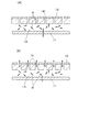
- the thermal noise in the air gap is noise generated by a mechanism as shown in FIG.
- the air gap 13 between the diaphragm 11 and the back plate 12, that is, the air molecule ⁇ in the semi-sealed space collides with the diaphragm 11 due to fluctuation (thermal motion).
- the diaphragm 11 is subjected to a minute force due to the collision with the air molecule ⁇ , and the minute force applied to the diaphragm 11 varies randomly. Therefore, the diaphragm 11 vibrates due to the collision of the air molecules ⁇ , and electrical noise is generated in the vibration sensor.
- noise due to such thermal noise is large and the S / N ratio is deteriorated.
- Such noise caused by thermal noise increases the opening ratio of the acoustic holes 14 opened in the back plate 12 as shown in FIG. 1B, and the air in the air gap 13 passes through the acoustic holes 14. It is reduced by making it easy to do. It can also be reduced by widening the air gap 13 between the diaphragm 11 and the back plate 12.
- the opening ratio of the acoustic hole 14 is increased or the air gap 13 is widened, the capacitance of the capacitor constituted by the diaphragm 11 and the back plate 12 is decreased. Therefore, in the method of simply reducing the noise, the sensitivity of the acoustic sensor is reduced at the same time as the noise is reduced, and the S / N ratio of the acoustic sensor cannot be improved.
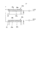
- Patent Document 1 discloses a differential detection type microphone for the purpose of improving the S / N ratio.
- the microphone 21 as shown in FIG. 2, two acoustic sensors 23a and 23b are provided on a single substrate 22, and the upper and lower configurations of the sensors 23a and 23b are reversed. That is, in one acoustic sensor 23a, a fixed plate 25a having an acoustic hole 26a is formed on the diaphragm 24a to constitute a capacitor for acoustic detection. In the other acoustic sensor 23b, a diaphragm 24b is formed on a fixed plate 25b having an acoustic hole 26b to constitute a capacitor for acoustic detection.
- both the acoustic sensors 23a and 23b output detection signals from the diaphragms 24a and 24b, when both the sensors 23a and 23b detect the same acoustic vibration, the sensors 23a and 23b are detected with a phase shifted by 180 °. A signal is output.
- the output of the acoustic sensor 23a and the output of the acoustic sensor 23b are input to a signal processing circuit (ASIC) and subtracted in the signal processing circuit.
- ASIC signal processing circuit
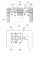
- Patent Document 2 discloses another conventional microphone.
- the microphone 31 basically has the same structure as the microphone 21 of Patent Document 1.
- a plurality of independent acoustic sensors 33a, 33b,... Having the same structure are provided on a common substrate 32 as shown in FIG. That is, any of the acoustic sensors 33a, 33b,... Is formed with the diaphragm 34 facing the upper surface of the fixed plate 35 having the acoustic holes 36 opened.
- a signal processing circuit 37 is provided on the upper surface of the substrate 32, and outputs of the respective acoustic sensors 33a, 33b,. To the signal processing circuit 37.
- the signal processing circuit 37 adds the output of each sensor 33a, 33b,. Is expected to improve.
- acoustic characteristics other than sensitivity are likely to be shifted between the sensors. For example, frequency characteristics, phase, and the like are affected by the back chamber and vent hole of each sensor, and therefore tend to have different characteristics among the sensors.
- the present invention has been made in view of the above technical problems, and an object of the present invention is to provide an acoustic sensor capable of improving the S / N ratio of the sensor without hindering downsizing of the sensor. And providing a microphone using the acoustic sensor.
- An acoustic sensor includes a substrate having a cavity, a thin film diaphragm disposed over the substrate so as to cover the cavity, a movable electrode plate formed on the diaphragm,
- An acoustic sensor comprising: a back plate fixed to the upper surface of the substrate so as to face the diaphragm; and a fixed electrode plate provided on the back plate at a position facing the movable electrode plate, the diaphragm and
- the movable electrode plate is substantially divided into a plurality of regions, and a plurality of capacitors connected in parallel are constituted by the divided movable electrode plates and the fixed electrode plate.
- the movable electrode plate may be provided on the diaphragm, or the diaphragm itself may be a movable electrode plate.
- the diaphragm is substantially divided into a plurality of regions, the capacitance and sensitivity to acoustic vibration are substantially unchanged from those before the diaphragm is divided. .
- each divided area of the diaphragm can move almost independently, each area displaces discontinuously independently of the thermal noise, and adding the noise in each area cancels the noise. Together, it gets smaller. As a result, the S / N ratio of the acoustic sensor is improved.
- the diaphragm is divided into a plurality of regions and the sound is detected in each region, downsizing of the acoustic sensor is not hindered.
- An embodiment of the acoustic sensor according to the present invention is characterized in that the diaphragm and the movable electrode plate are divided by slits.
- the openings of the diaphragm and the movable electrode plate are widened, air easily passes through the diaphragm and the movable electrode plate, and the low frequency characteristics of the acoustic sensor are deteriorated.
- the diaphragm and the movable electrode plate are divided by the slits, the opening for dividing the diaphragm and the movable electrode plate can be narrowed, the deterioration of the low frequency characteristics of the acoustic sensor is prevented, and the sensitivity is reduced. Can be prevented.
- the slit is formed at a position passing through the maximum displacement portion of the diaphragm.
- the slit is provided so as to pass through the maximum displacement portion of the diaphragm, the effect of improving the S / N ratio of the acoustic sensor can be increased.
- each region of the diaphragm divided by the slits has a maximum displacement portion across the slit.
- each area of the divided diaphragm has a maximum displacement portion across the slit, so that the effect of improving the S / N ratio of the acoustic sensor can be increased.
- the slit is located on a line segment connecting any two support portions of the support portions of the diaphragm.
- the slit is formed on the line segment connecting the support portions of the diaphragm, the displacement of the end of the slit can be reduced, and the stress concentration at the end of the slit can be reduced.
- the slit is partially interrupted, and each region of the diaphragm located on both sides of the slit is an interrupted portion of the slit. May be partially connected through.
- the width of the slit is 10 ⁇ m or less.
- the roll-off frequency may be as high as 500 Hz and the low-frequency characteristics may be deteriorated. Therefore, the slit width is 10 ⁇ m or less as in the embodiment. It is desirable that
- the length of the slit is 1 ⁇ 2 or more of the passing length of the diaphragm in the extending direction of the slit. If the slit length is shorter than 1 ⁇ 2 of the diaphragm width, the discontinuity of displacement between the regions of the diaphragm divided by the slit is impaired, and the effect of reducing noise as a whole becomes worse. It is desirable that it is 1 ⁇ 2 or more of the diaphragm passing length in the extending direction.
- the shape of the diaphragm is not particularly limited, but it is desirable to use a circular or rectangular diaphragm in view of the characteristics of the acoustic sensor.
- Still another embodiment of the acoustic sensor according to the present invention is such that the diaphragm is supported by the substrate or the back plate at a plurality of positions of the diaphragm, and at least one of the support positions between adjacent support positions. It is characterized in that voids are formed at the locations.
- the diaphragm is partially fixed, so that the spring property of the diaphragm is reduced. It can be prevented from becoming high, and the sensitivity of the acoustic sensor can be prevented from being lowered.
- gap between support locations can be utilized as a bench hole.
- Still another embodiment of the acoustic sensor according to the present invention is characterized in that acoustic vibration reaches the diaphragm through the cavity.
- the cavity in the substrate becomes the front chamber, and the space outside the acoustic sensor becomes the back chamber. Therefore, the volume of the back chamber can be increased, and the sensitivity of the acoustic sensor can be improved.
- the microphone according to the present invention includes the acoustic sensor according to the present invention and a circuit for processing a signal output from the acoustic sensor. Since the microphone of the present invention uses the acoustic sensor of the present invention, the S / N ratio of the microphone can be improved.
- the means for solving the above-described problems in the present invention has a feature in which the above-described constituent elements are appropriately combined, and the present invention enables many variations by combining such constituent elements. .
- FIG. 1A and FIG. 1B are schematic diagrams for explaining thermal noise of an acoustic sensor.
- FIG. 2 is a schematic explanatory diagram of the microphone disclosed in Patent Document 1.
- FIG. 3A and 3B are a cross-sectional view and a plan view of the microphone disclosed in Patent Document 2, respectively.
- FIG. 4 is a cross-sectional view of the acoustic sensor according to Embodiment 1 of the present invention.
- FIG. 5 is a plan view of the acoustic sensor according to the first embodiment.
- FIG. 6 is a plan view showing the shape of the diaphragm in the acoustic sensor of the first embodiment.
- FIG. 7 is a diagram showing an equivalent circuit obtained by simplifying the acoustic sensor.
- FIG. 1A and FIG. 1B are schematic diagrams for explaining thermal noise of an acoustic sensor.
- FIG. 2 is a schematic explanatory diagram of the microphone disclosed in Patent Document 1.
- FIG. 3A and 3B are
- FIG. 8 is an equivalent circuit diagram showing a situation in which acoustic vibration and noise are applied to only one acoustic sensing unit.
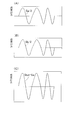
- FIG. 9A is a waveform diagram showing a sensitivity signal output from the acoustic sensor when acoustic vibration is applied to only one acoustic sensing unit.
- FIG. 9B is a waveform diagram showing a sensitivity signal output from the acoustic sensor when acoustic vibration is applied only to the other acoustic sensing unit.
- FIG. 9C is a waveform diagram showing a sensitivity signal output from the acoustic sensor when acoustic signals are simultaneously applied to both acoustic sensing units.
- FIG. 9A is a waveform diagram showing a sensitivity signal output from the acoustic sensor when acoustic vibration is applied to only one acoustic sensing unit.
- FIG. 9B is a waveform diagram showing a sensitivity signal output from the acous
- FIG. 10A is a waveform diagram showing a noise signal output from the acoustic sensor when noise occurs only in one acoustic sensing unit.
- FIG. 10B is a waveform diagram showing a noise signal output from the acoustic sensor when noise occurs only in the other acoustic sensing unit.
- FIG. 10C is a waveform diagram showing a noise signal output from the acoustic sensor when noise is simultaneously generated in both acoustic sensing units.
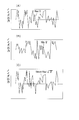
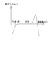
- FIG. 11 is a diagram for explaining the roll-off frequency.
- FIG. 12 is a plan view showing an acoustic sensor according to Embodiment 2 of the present invention.
- FIG. 13 is a plan view showing the shape of the diaphragm in the acoustic sensor of the second embodiment.
- FIG. 14 is a cross-sectional view showing an acoustic sensor according to Embodiment 3 of the present invention.
- FIG. 15 is a plan view of the acoustic sensor according to the third embodiment.
- FIG. 16 is an exploded perspective view of an acoustic sensor according to Embodiment 4 of the present invention.
- FIG. 17 is a plan view showing the shape of a diaphragm in the acoustic sensor of the fourth embodiment.
- FIG. 18 is a plan view of an acoustic sensor according to Embodiment 5 of the present invention.
- FIG. 19 is a plan view illustrating the shape of a diaphragm in the acoustic sensor according to the fifth embodiment.
- FIG. 20 is a plan view showing the shape of a diaphragm in a modification of the fifth embodiment.
- FIG. 21 is a plan view showing the shape of the diaphragm in the acoustic sensor according to the sixth embodiment of the present invention.
- FIG. 22 is a plan view showing different shapes of the diaphragm in the acoustic sensor of the sixth embodiment.
- FIG. 23 is a plan view showing the shape of a diaphragm in an acoustic sensor according to Embodiment 7 of the present invention.
- FIG. 24 is a cross-sectional view of a microphone according to Embodiment 8 of the present invention.
- FIG. 25 is a plan view of the microphone of the eighth embodiment with the cover removed.
- FIG. 26 is a cross-sectional view showing microphones having different structures in the eighth embodiment.
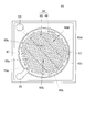
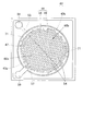
- FIG. 4 is a cross-sectional view showing the acoustic sensor 41 of the first embodiment.
- FIG. 5 is a plan view of the acoustic sensor 41.
- FIG. 6 is a plan view of the acoustic sensor 41 with the canopy 44 removed.
- the acoustic sensor 41 is a capacitive element manufactured using MEMS technology. As shown in FIG. 4, in the acoustic sensor 41, a diaphragm 43 (vibrating electrode plate) is provided on an upper surface of a silicon substrate 42 (semiconductor substrate) via an anchor 46, and a minute air gap (gap) 50 is formed thereon. The canopy 44 is fixed through the gap.
- a back chamber 45 (cavity) penetrating from the front surface to the back surface is opened in the silicon substrate 42 made of single crystal silicon.
- the inner surface of the back chamber 45 may be a vertical surface, or may be inclined in a tapered shape.
- a plurality of anchors 46 for supporting the lower surface of the outer peripheral edge of the diaphragm 43 are provided on the upper surface of the silicon substrate 42 at substantially equal intervals. Further, a base portion 51 is formed on the upper surface of the silicon substrate 42 so as to surround the diaphragm 43. Anchor 46 and base portion 51 is formed by SiO 2.
- the diaphragm 43 is formed in a substantially circular shape.
- the diaphragm 43 is formed of a conductive polysilicon thin film, and the diaphragm 43 itself is a movable electrode plate.
- the diaphragm 43 is disposed on the silicon substrate 42 so as to cover the back chamber 45 and is supported on the substrate 42 at substantially equal intervals by an anchor 46. Therefore, the diaphragm 43 is supported in the air, and a narrow vent hole 52 for allowing acoustic vibrations to pass between the adjacent anchors 46 is between the lower surface of the outer peripheral portion of the diaphragm 43 and the upper surface of the silicon substrate 42. Is formed. Further, a strip-like lead wiring 53 extends outward from the diaphragm 43.
- the diaphragms 43 are supported at equal intervals by the anchors 46 as described above, and the vent holes 52 (voids) are formed between the anchors 46.
- the diaphragm 43 is equally divided into two by a narrow linear slit 47 whose position is determined so as to pass through the center which is the maximum displacement point. However, the diaphragm 43 is not completely divided into two by the slit 47 but is mechanically and electrically connected in the vicinity of the end of the slit 47.
- diaphragms 43a and 43b the two semicircular regions of the diaphragm 43 divided by the slit 47. Both diaphragms 43a and 43b are formed in the same shape and the same dimensions.
- the canopy 44 is provided with a fixed electrode plate 49 made of polysilicon on the lower surface of a back plate 48 (fixed film) made of SiN.
- the canopy portion 44 is formed in a dome shape and has a hollow portion below it, and covers the diaphragm 43 with the hollow portion.
- a minute air gap 50 is formed between the lower surface of the canopy 44 (that is, the lower surface of the fixed electrode plate 49) and the upper surface of the diaphragm 43.
- the fixed electrode plate 49 and the diaphragm 43 are opposed to each other to constitute a capacitor.
- acoustic holes 54 for passing acoustic vibrations are drilled in almost the entire canopy 44 so as to penetrate from the upper surface to the lower surface. As shown in FIGS. 4 and 5, the acoustic holes 54 are regularly arranged. In the illustrated example, the acoustic holes 54 are arranged in a triangular shape along three directions forming an angle of 120 ° with each other, but may be arranged in a rectangular shape or a concentric shape.
- a cylindrical stopper 55 protrusion protrudes from the bottom surface of the canopy 44.
- the stopper 55 projects integrally from the lower surface of the back plate 48, penetrates the fixed electrode plate 49, and projects to the lower surface of the canopy 44. Since the stopper 55 is made of SiN like the back plate 48, it has an insulating property.
- the stopper 55 is for preventing the diaphragm 43 from being fixed to the fixed electrode plate 49 due to electrostatic force and not being separated.
- the protective film 56 extends continuously from the outer periphery of the canopy-shaped back plate 48 over the entire circumference.
- the protective film 56 covers the base portion 51 and the outer region.
- the lead-out wiring 53 is fixed to the base portion 51, and the lead-out wiring 57 extended from the fixed electrode plate 49 is also fixed to the upper surface of the base portion 51.
- an opening is formed in the protective film 56, and a movable electrode pad 58 is formed on the upper surface of the lead wiring 53 through the opening, and the movable electrode pad 58 is electrically connected to the diaphragm 43 through the lead wiring 53.
- the fixed electrode pad 59 provided on the upper surface of the back plate 48 is electrically connected to the lead wiring 57 through a through hole and the like, and is further electrically connected to the fixed electrode plate 49.
- the diaphragm 43 is divided into a diaphragm 43a and a diaphragm 43b. Therefore, between the common canopy portion 44 and the back chamber 45, one acoustic sensing portion 60a is constituted by a capacitor formed of a region facing the diaphragm 43a in the diaphragm 43a and the fixed electrode plate 49. Further, the other acoustic sensing unit 60b is configured by a capacitor formed of a region facing the diaphragm 43b in the diaphragm 43b and the fixed electrode plate 49. In addition, both the sensing units 60a and 60b are integrally formed at the same location in the canopy 44, have the same structure, the same shape, and the same dimensions, and have substantially the same characteristics.
- the diaphragms 43a and 43b which are thin films, vibrate in the same phase due to the acoustic vibration.
- the diaphragms 43a and 43b vibrate and the gap distances between the diaphragms 43a and 43b and the fixed electrode plate 49 change, the capacitances of the sensing units 60a and 60b change.
- the acoustic vibration (change in sound pressure) sensed by the diaphragms 43a and 43b becomes a change in the capacitance between the diaphragms 43a and 43b and the fixed electrode plate 49, Output as a typical signal.
- the diaphragms 43a and 43b are both connected to the movable electrode pad 58 and the fixed electrode plate 49 is common, the acoustic sensing unit 60a (capacitor) and the acoustic sensing unit 60b (capacitor) are electrically connected. Are connected in parallel.
- the diaphragm 43a and the diaphragm 43b are electrically connected, and the fixed electrode plate 49 is common.
- the acoustic sensing units 60a and 60b are provided at the same position on the substrate 42, and both the sensing units 60a and 60b detect acoustic vibrations in the same phase. Therefore, even if the diaphragms 43 a and 43 b are separated by the slit 47, the capacitance and sensitivity to the acoustic vibration of the acoustic sensor 41 are not substantially changed from those before the slit 47 is formed.
- the diaphragms 43a and 43b are divided by the slit 47 and can move substantially independently, the displacement of the diaphragms 43a and 43b on both sides of the slit 47 can be discontinuous. Therefore, the thermal noise generated in the acoustic sensing unit 60a and the thermal noise generated in the acoustic sensing unit 60b are detected as signals having different phases. Therefore, when noises of both the sensing units 60a and 60b are added together, the noises cancel each other and become smaller. As a result, the S / N ratio of the acoustic sensor 41 is improved.
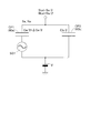
- FIG. 7 shows an equivalent circuit in which the acoustic sensor 41 is simplified.
- the two acoustic sensing units 60a and 60b separated by the slit 47 can be represented by two variable capacitors CP1 and CP2 connected in parallel.
- the two variable capacitors CP1 and CP2 have the same performance.
- signal generation sources such as acoustic vibration and noise are represented by respective AC power sources SG1 and SG2 connected in series to the variable capacitors CP1 and CP2.
- the acoustic sensing unit 60a is represented by a circuit in which the variable capacitor CP1 and the AC power source SG1 are connected in series
- the acoustic sensing unit 60b is a circuit in which the variable capacitor CP2 and the AC power source SG2 are connected in series. It is represented by Furthermore, the acoustic sensor 41 is represented by an equivalent circuit in which both series connection circuits are connected in parallel.
- the characteristic or circuit constant in the equivalent circuit of FIG. 7 is represented by the following symbols.
- FIG. 8 a situation is considered in which acoustic vibration and noise are added only to the acoustic sensing unit 60a. Since no signal due to acoustic vibration or noise is generated in the acoustic sensing unit 60b, the AC power source SG2 of the acoustic sensing unit 60b is omitted, and it is considered that the capacitance of the variable capacitor CP1 does not change.
- the sensitivity output output from the acoustic sensing unit 60a is as described above.
- Sa V ⁇ ⁇ Ca / Ca It becomes.
- the capacitor CP2 of the acoustic sensing unit 60b is connected in parallel to the acoustic sensing unit 60a, the capacitor CP2 functions as a parasitic capacitance with respect to the acoustic sensing unit 60a and attenuates the sensitivity of the acoustic sensing unit 60a.
- the sensitivity output Stot output from the acoustic sensor 41 is the sensitivity output Sb of the acoustic sensing unit 60b in the same manner as in FIG. Is halved to the following formula.
- sensitivity outputs Sa and Sb and noise outputs Na and Nb are simultaneously generated in the acoustic sensing units 60a and 60b as shown in FIG.
- the sensitivity output is such that the diaphragms 43a and 43b that detect acoustic vibrations are arranged in close proximity within the same canopy 44, so that both diaphragms 43a and 43b vibrate with the same phase and amplitude at the same time. is doing.
- the variable capacitor CP1 of the acoustic sensing unit 60a and the variable capacitor CP2 of the acoustic sensing unit 60b are connected in parallel.
- the sensitivity output Stot of the acoustic sensor 41 is the sum of the sensitivity outputs Sa / 2 and Sb / 2 of the acoustic sensing units 60a and 60b obtained above.
- Stot Sa / 2 + Sb / 2
- the acoustic sensor 41 has two signals having the same phase and amplitude (sensitivity output Sa / 2 in FIGS. 9A and 9B).
- the noise output Ntot output from the acoustic sensor 41 includes the noise output Na / 2 output from the acoustic sensing unit 60a and the noise output Nb / output from the acoustic sensing unit 60b, as shown in FIG. It is calculated
- required by the calculation at the time of adding the variance with 2. That is, the following equation is obtained. Stot ⁇ ⁇ (Na / 2) 2 + (Nb / 2) 2 ⁇
- Na Nb
- the sensitivity output Stot of the acoustic sensor 41 is added, and the noise output Ntot is obtained by calculation when the variance is added.
- the S / N ratio of the acoustic sensor 41 becomes ⁇ (2) Sa / Na, and the S / N ratio becomes ⁇ (2) times as compared with the case where the slit 47 is not provided (or improved by 3 dB). To do).
- the noise output decreased by 3 dB by providing the slit 47. Therefore, the S / N ratio was increased by +3 dB by providing the slit 47.
- the S / N ratio of the acoustic sensor 41 can be improved by providing the diaphragm 47 with the slit 47.
- the length L of the slit 47 (see FIG. 6) desirably crosses the width of the diaphragm 43 by 50% or more. That is, it is desirable that the length L of the slit 47 is 1 ⁇ 2 or more of the width of the diaphragm 43 on the line extending the slit 47.
- the slit 47 is provided to isolate the displacement on the diaphragm 43a side and the displacement on the diaphragm 43b side so as to be discontinuous.
- the diaphragm 47 is provided. This is because the discontinuity of displacement on the 43a side and the diaphragm 43b side is impaired.
- the width W of the slit 47 (see FIG. 6) is preferably 10 ⁇ m or less. This is because if the width W of the slit 47 is too wide, the amount of air leaking from the air gap 50 to the back chamber 45 through the slit 47 increases, the roll-off frequency is increased, and the low frequency characteristics of the acoustic sensor 41 are deteriorated. As shown in FIG. 11, the roll-off frequency Froll-off is a frequency at which the sensitivity output is lowered by a certain decibel on the low frequency side.
- Froll-off 1 / 1 / (Rventholl / Cbackchamber) Therefore, when the width W of the slit 47 is increased, the acoustic resistance Rventhole is decreased, the roll-off frequency Froll-off is increased, and the low frequency characteristics of the acoustic sensor 41 are deteriorated.
- the acoustic resistance Rventhole is also affected by the length L of the slit 47.
- the roll-off frequency Froll-off is 50 Hz or less, and when the width of the slit 47 is 10 ⁇ m, the roll-off is performed.
- the frequency Froll-off is 500 Hz.
- the width W of the slit 47 is 10 ⁇ m or less. It is desirable.
- the resultant force of the pressure applied to each part of the diaphragm due to thermal noise acts on the maximum displacement location of the diaphragm if the diaphragm has rigidity. Since the maximum displacement position of the diaphragm 43 before the slit 47 is formed is at the center thereof, the slit 47 is formed so as to pass through the center of the diaphragm 43, and each of the divided diaphragms 43a and 43b It is desirable to have maximum displacement points on both sides.
- the diaphragms 43a and 43b have the same shape and the same dimensions, and the acoustic sensing units 60a and 60b have substantially the same characteristics.
- the present invention is not necessarily limited to such an embodiment.
- the diaphragm 43a and the diaphragm 43b have different shapes or different dimensions, and the acoustic sensing unit 60a and the acoustic sensing unit 60b have different characteristics. You can do it.
- FIG. 12 shows a plan view of an acoustic sensor 61 according to Embodiment 2 of the present invention.
- FIG. 13 is a plan view of the acoustic sensor 61 with the canopy 44 removed.
- a plurality of (three in the illustrated example) slits 47 are provided in the diaphragm 43, and the diaphragm 43 is divided into three or more regions (four regions in the illustrated example), which are substantially independent.
- a plurality of diaphragms 43a, 43b,... are provided.
- the diaphragms 43a, 43b,... And a common fixed electrode plate 49 constitute a plurality of acoustic sensing units 60a, 60b,.
- the acoustic sensor 61 according to the second embodiment has a larger number of divisions of the diaphragm 43 than the acoustic sensor 41 according to the first embodiment. Even when the number of slits 47 is increased and the number of divisions of the diaphragm 43 is increased in this way (the shape and area of each diaphragm 43a, 43b,... May be different), the sound is sounded for the same reason as in the first embodiment.
- the S / N ratio of the sensor 61 can be increased. Further, if the number of divisions of the diaphragm 43 is increased, the effect of further reducing the noise of the acoustic sensor 61 and improving the S / N ratio becomes higher.
- FIG. 14 is a cross-sectional view of an acoustic sensor 62 according to Embodiment 3 of the present invention.
- FIG. 15 is a plan view of the acoustic sensor 62 according to the third embodiment.
- the diaphragm 43 is not supported by the anchor 46 as in the first embodiment, and is simply placed on the upper surface of the silicon substrate 42.
- a protrusion 71 for contacting the upper surface of the diaphragm 43 is projected downward from a position on the lower surface of the back plate 48 facing the outer peripheral portion of the diaphragm 43. Therefore, when a voltage is applied between the diaphragm 43 and the fixed electrode plate 49, the diaphragm 43 is pulled up toward the fixed electrode plate 49 by electrostatic attraction.
- the diaphragm 43 pulled upward is in contact with and fixed to the lower end surface of the protrusion 71, and an air gap 50 is formed between the diaphragm 43 and the fixed electrode plate 49.
- an air gap 50 is formed between the diaphragm 43 and the fixed electrode plate 49.
- the diaphragm 43 is provided with one (or a plurality of) slits 47, and the two diaphragms 43a and 43b and the fixed electrode plate 49 form two acoustic sensing units 60a and acoustic sensing. Part 60b is configured. Therefore, even in this acoustic sensor 62, the S / N ratio of the acoustic sensor 62 is improved in the same manner as in the first embodiment.
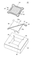
- FIG. 16 is an exploded perspective view of the acoustic sensor 63 according to the fourth embodiment of the present invention.
- FIG. 17 is a plan view of the acoustic sensor 63 with the canopy 44 removed.
- This acoustic sensor 63 uses a rectangular diaphragm 34.
- a prismatic back chamber 45 is opened in the silicon substrate 42, and a diaphragm 43 is disposed on the upper surface of the silicon substrate 42 so as to cover the upper surface opening of the back chamber 45.
- Legs 72 are provided at the four corners of the diaphragm 43, and each leg 72 is fixed to the diaphragm 43 by an anchor 46 provided on the upper surface of the silicon substrate 42.
- the diaphragm 43 is divided into diaphragms 43 a and 43 b by diagonal slits 47.
- the canopy 44 is also formed in a substantially rectangular shape so as to cover the rectangular diaphragm 43.
- the broken line in FIG. 17 represents the amount of displacement when the diaphragm 43 is displaced by acoustic vibration, as a contour line, and the amount of displacement increases toward the center.
- the center is the maximum displacement portion, and if the slit 47 is formed so as to pass through the maximum displacement portion of the diaphragm 43, the S / N ratio improvement effect of the acoustic sensor 63 is achieved. Can be increased.
- FIG. 18 is a plan view of an acoustic sensor 64 according to Embodiment 5 of the present invention.
- FIG. 19 is a plan view of the acoustic sensor 64 with the canopy 44 removed.
- a slit 47 is formed from end to end of the diaphragm 43 so as to pass through the center of the diaphragm 43. Therefore, the diaphragm 43 is completely separated into two diaphragms 43 a and 43 b by the slit 47. The diaphragms 43a and 43b thus separated are connected by a bifurcated lead-out wiring 53 formed on the upper surface of the silicon substrate.
- the lead wires 53a and 53b may be separately provided in the diaphragms 43a and 43b.
- the lead wires 53a and 53b may be connected outside the acoustic sensor or may be connected in a signal processing circuit (ASIC).
- the slit 47 When providing the slit 47 in the diaphragm 43, it is preferable to provide the diaphragm 43 so as to pass through the maximum displacement portion of the diaphragm 43, but the direction of the slit 47 is not particularly limited.
- the slits 47 are provided in the direction connecting the fixed portions of the rectangular diaphragm 43, that is, in the diagonal direction of the diaphragm 43, but the present invention is not necessarily limited thereto.
- the slit 47 may be formed in a direction parallel to the side of the rectangular diaphragm 43. In this case, since the center of the left and right vent holes 52 is connected, the divided diaphragms 43a and 43b are both supported in a cantilever shape.
- the slit 47 may be inclined from a diagonal direction of the diaphragm 43 or a direction parallel to the side.
- the diaphragms formed on both sides of the slit may be partially connected through the slit.
- one slit 47 is partially interrupted, and the two slits 47 are arranged in a straight line. Therefore, the diaphragms 43 a and 43 b located on both sides of the slit 47 are partially connected through the interrupted portion of the slit 47. Even if it is such a form, if the length of the part in which the slit 47 is interrupted is not so long, there is no problem.
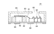
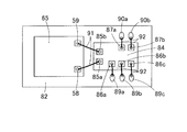
- FIG. 24 is a cross-sectional view of a MEMS microphone using the acoustic sensor of each of the above embodiments.
- FIG. 25 is a plan view of the microphone with the cover removed.
- the microphone 81 is a package in which an acoustic sensor 65 and a signal processing circuit 84 (ASIC) are built in a package including a circuit board 82 and a cover 83.
- the acoustic sensor 65 and the signal processing circuit 84 are mounted on the upper surface of the circuit board 82.
- the electrode pads 58 and 59 of the acoustic sensor 65 are connected to the pads 85a and 85b of the signal processing circuit 84 by bonding wires 91, respectively.
- a plurality of terminals 88 for electrically connecting the microphone 81 to the outside are provided on the lower surface of the circuit board 82, and electrode portions 89a-89c; 90a, 90b electrically connected to the terminals 88 are provided on the upper surface of the circuit board 82.
- the 84 pads 86a-86c; 87a, 87b mounted on the circuit board 82 are connected to the electrode portions 89a-89c; 90a, 90b by bonding wires 92, respectively.
- the pads of the signal processing circuit 84 have a function of supplying power to the acoustic sensor 65 and a function of outputting a capacitance change signal of the acoustic sensor 65 to the outside.
- a cover 83 is attached to the upper surface of the circuit board 82 so as to cover the acoustic sensor 65 and the signal processing circuit 84.
- a sound introduction hole 93 for introducing acoustic vibration into the package is opened.
- the package also has an electromagnetic shielding function, and protects the microphone 81 from external electrical disturbances and mechanical shocks.
- the acoustic vibration that has entered the package through the sound introduction hole 93 is detected by the acoustic sensor 65 and is output after being subjected to predetermined signal processing by the signal processing circuit 84.
- the acoustic sensor according to the present invention is used as the acoustic sensor 65, the microphone 81 has a high S / N ratio.
- FIG. 26 shows a microphone 94 having another structure.
- the sound introduction hole 93 is opened in the circuit board 82 at a position facing the lower surface of the cavity of the silicon substrate 42, not the cover 83.
- the cavity of the silicon substrate 42 becomes the front chamber 95, and the space inside the package becomes the back chamber 45. Therefore, according to such an embodiment, the volume of the back chamber 45 can be increased, and the sensitivity of the microphone 81 can be further improved.
Landscapes
- Physics & Mathematics (AREA)
- Acoustics & Sound (AREA)
- Engineering & Computer Science (AREA)
- Signal Processing (AREA)
- General Physics & Mathematics (AREA)
- Electrostatic, Electromagnetic, Magneto- Strictive, And Variable-Resistance Transducers (AREA)
- Pressure Sensors (AREA)
- Micromachines (AREA)
Abstract
Description
特許文献1には、S/N比を向上させることを目的とした差分検知方式のマイクロフォンが開示されている。このマイクロフォン21では、図2に示すように、一枚の基板22に2つの音響センサ23a、23bが設けられていて、両センサ23a、23bは上下の構成が反転している。すなわち、一方の音響センサ23aでは、ダイアフラム24aの上に音響孔26aを有する固定プレート25aが形成されていて音響検知用のキャパシタが構成されている。他方の音響センサ23bでは、音響孔26bを有する固定プレート25bの上にダイアフラム24bが形成されていて音響検知用のキャパシタが構成されている。
特許文献2には、従来の別なマイクロフォンが開示されている。このマイクロフォン31は、基本的には、特許文献1のマイクロフォン21と同様な構造を有している。特許文献2のマイクロフォン31では、図3(A)に示すように、共通の基板32の上に同じ構造を有する独立した複数個の音響センサ33a、33b、…が設けられている。すなわち、いずれの音響センサ33a、33b、…も、音響孔36を開口された固定プレート35の上面に対向させてダイアフラム34が形成されている。さらに、図3(B)に示すように、基板32の上面には信号処理回路37が設けられており、各音響センサ33a、33b、…の出力は基板32上に配線された電極引出線38を通じて信号処理回路37に接続されている。このマイクロフォン31の場合には、各音響センサ33a、33b、…が同じ構造を有しているので、各センサ33a、33b、…の出力を信号処理回路37において加算処理することによってS/N比を向上させることが期待される。
図4-図6を参照して本発明の実施形態1による音響センサの構造を説明する。図4は実施形態1の音響センサ41を示す断面図である。図5は、音響センサ41の平面図である。また、図6は、音響センサ41から天蓋部44を取り除いた状態の平面図である。
Ca/2[F] :可変キャパシタCP1の静電容量
Cb/2[F] :可変キャパシタCP2の静電容量
ΔCa/2[F] :可変キャパシタCP1の受圧時の静電容量変化
ΔCb/2[F] :可変キャパシタCP2の受圧時の静電容量変化
V[V] :音響センサ41への印加電圧
Sa[V] :音響センシング部60aの感度出力
Sb[V] :音響センシング部60bの感度出力
Na[V] :音響センシング部60aのノイズ出力
Nb[V] :音響センシング部60bのノイズ出力
Sa/Na :音響センシング部60aのS/N比
Sb/Nb :音響センシング部60bのS/N比
ここで、感度出力とは、交流電源で発生した音響振動によって音響センシング部(あるいは、可変キャパシタ)から出る信号出力であって、電圧×固定キャパシタの静電容量変化/固定キャパシタの静電容量で表される。したがって、音響センシング部60aの感度出力は、
Sa=V×(ΔCa/2)/(Ca/2)=V×ΔCa/Ca
となる。同様に、音響センシング部60bの感度出力は、
Sb=V×(ΔCb/2)/(Cb/2)=V×ΔCb/Cb
となる。
Sa=V×ΔCa/Ca
となる。しかし、この音響センシング部60aには、音響センシング部60bのキャパシタCP2が並列に接続されているので、キャパシタCP2は音響センシング部60aに対しては寄生容量として働き、音響センシング部60aの感度を減衰させる。キャパシタCP1とCP2は同じ静電容量を有しているので、音響センサ41から出力される感度出力(すなわち、信号処理回路へ入力される感度出力)Stotは、次式で表されるように半減する。
Stot=〔(Ca/2)/{(Ca/2)+(Cb/2)}〕×Sa
=Sa/2
Ntot=〔(Ca/2)/{(Ca/2)+(Cb/2)}〕×Na
=Na/2
Stot=〔(Cb/2)/{(Cb/2)+(Ca/2)}〕×Sb
=Sb/2
Ntot=〔(Cb/2)/{(Cb/2)+(Ca/2)}〕×Nb
=Nb/2
Stot=Sa/2+Sb/2
ここで、Sa=Sbであるから、上式は、
Stot=Sa
となる。これは、図9(A)-図9(C)に示すように、音響センサ41では、位相と振幅が同じ2つの信号(図9(A)及び図9(B)の感度出力Sa/2、Sb/2)が重ね合わされたものが全体の感度出力Stot=Sa(図9(C))として出力されることを表し、スリット47を設けても音響センサ41の感度出力Stotはスリット47を設ける前と変わりがないことを示している。
Stot=√{(Na/2)2+(Nb/2)2}
ここで、Na=Nbであるから、上式は、
Stot=Na/√(2)
となる。
Froll-off ∝ 1/(Rventholl・Cbackchamber)
従って、スリット47の幅Wが大きくなると音響抵抗Rventholeが小さくなり、ロールオフ周波数Froll-offが高くなり、音響センサ41の低周波特性が悪くなる。音響抵抗Rventholeはスリット47の長さLにも影響されるが、例えばスリット47の幅Wが1μmであればロールオフ周波数Froll-offは50Hz以下であり、スリット47の幅が10μmになるとロールオフ周波数Froll-offは500Hzにもなる。このようにスリット47の幅が10μmを超えると著しくロールオフ周波数が高くなって低周波特性が悪化し、音響センサ41の感度が大きく損なわれてしまうので、スリット47の幅Wは10μm以下であることが望ましい。
図12に本発明の実施形態2による音響センサ61の平面図を示す。図13は、天蓋部44を除いた状態における音響センサ61の平面図である。
図14は本発明の実施形態3による音響センサ62の断面図である。図15は、実施形態3の音響センサ62の平面図である。
図16は、本発明の実施形態4による音響センサ63の分解斜視図である。図17は、音響センサ63の、天蓋部44を取り除いた状態の平面図である。
図18は、本発明の実施形態5による音響センサ64の平面図である。図19は、音響センサ64の、天蓋部44を取り除いた状態の平面図である。
ダイアフラム43にスリット47を設ける場合には、ダイアフラム43の最大変位箇所を通過するように設けることが好ましいが、スリット47の方向については特に限定されるものではない。たとえば、実施形態4の音響センサ63では、矩形状のダイアフラム43の固定箇所を結ぶ方向、すなわちダイアフラム43の対角方向にスリット47を設けたが、必ずしもこれに限るものではない。図21に示すように、矩形状のダイアフラム43の辺と平行な方向にスリット47を形成してもよい。この場合には、左右のベントホール52の中央を結ぶ方向となるので、分割されたダイアフラム43a、43bはいずれも片持ち梁状に支持されることになる。
スリットの両側に形成される各ダイアフラムは、スリットを通過して一部つながっていても差し支えない。たとえば、図23に示す実施形態では、1本のスリット47が部分的に途切れていて、2本のスリット47が直線状に並んだようになっている。したがって、スリット47を挟んでその両側に位置するダイアフラム43a、43bどうしは、スリット47の途切れた部分を通して部分的につながっている。このような形態であっても、スリット47の途切れている部分の長さがあまり長くなければ問題ない。
図24は上記各実施形態の音響センサを用いたMEMSマイクロフォンの断面図である。また、図25は、カバーを外した状態のマイクロフォンの平面図である。
43、43a、43b: ダイアフラム、 44: 天蓋部、
45: バックチャンバ、 46: アンカー、
47: スリット、 49: 固定電極板、
50: エアギャップ、 52: ベントホール、
60a、60b: 音響センシング部、 81、94: マイクロフォン、
82: 回路基板、 83: カバー、 84: 信号処理回路
Claims (13)
- 空洞部を有する基板と、
前記空洞部を覆うようにして前記基板の上方に配設された薄膜状のダイアフラムと、
前記ダイアフラムに形成された可動電極板と、
前記ダイアフラムに対向させるようにして前記基板の上面に固定されたバックプレートと、
前記可動電極板と対向する位置において前記バックプレートに設けた固定電極板とを備えた音響センサであって、
前記ダイアフラム及び前記可動電極板が複数領域に実質的に分割されていて、分割された各可動電極板と前記固定電極板によって複数個の並列に接続されたキャパシタが構成されていることを特徴とする音響センサ。 - 前記ダイアフラム及び前記可動電極板は、スリットによって分割されていることを特徴とする、請求項1に記載の音響センサ。
- 前記スリットは、前記ダイアフラムの最大変位箇所を通過する位置に形成されていることを特徴とする、請求項2に記載の音響センサ。
- 前記スリットによって分割された前記ダイアフラムの各領域は、前記スリットを挟んでそれぞれ最大変位箇所を有していることを特徴とする、請求項2に記載の音響センサ。
- 前記スリットは、前記ダイアフラムの支持箇所のうちいずれか2つの支持箇所を結ぶ線分上に位置していることを特徴とする、請求項2に記載の音響センサ。
- 前記スリットが部分的に途切れていて、当該スリットを挟んでその両側に位置するダイアフラムの各領域どうしが当該スリットの途切れた部分を通して部分的につながっていることを特徴とする、請求項2に記載の音響センサ。
- 前記スリットの幅が10μm以下であることを特徴とする、請求項2に記載の音響センサ。
- 前記スリットの長さは、当該スリットの延長方向における前記ダイアフラムの差し渡し長さの1/2以上であることを特徴とする、請求項2に記載の音響センサ。
- 前記ダイアフラムが円形状であることを特徴とする、請求項1に記載の音響センサ。
- 前記ダイアフラムが矩形状であることを特徴とする、請求項1に記載の音響センサ。
- 前記ダイアフラムは、その縁を複数箇所で前記基板又は前記バックプレートに支持されており、当該支持箇所のうち隣接する支持箇所の間の少なくとも一箇所に空隙が形成されていることを特徴とする、請求項1に記載の音響センサ。
- 音響振動が前記空洞部を通って前記ダイアフラムに到達することを特徴とする、請求項1に記載の音響センサ。
- 請求項1に記載した音響センサと、前記音響センサから出力された信号を処理するための回路とを備えたマイクロフォン。
Priority Applications (4)
| Application Number | Priority Date | Filing Date | Title |
|---|---|---|---|
| CN201180001987.3A CN102771143B (zh) | 2011-02-23 | 2011-03-16 | 声音传感器与麦克风 |
| KR1020117025833A KR101318332B1 (ko) | 2011-02-23 | 2011-03-16 | 음파센서 및 마이크로폰 |
| EP11770990.7A EP2519030B1 (en) | 2011-02-23 | 2011-03-16 | Acoustic sensor and microphone |
| US13/318,261 US8351625B2 (en) | 2011-02-23 | 2011-03-16 | Acoustic sensor and microphone |
Applications Claiming Priority (2)
| Application Number | Priority Date | Filing Date | Title |
|---|---|---|---|
| JP2011036903A JP4924853B1 (ja) | 2011-02-23 | 2011-02-23 | 音響センサ及びマイクロフォン |
| JP2011-036903 | 2011-02-23 |
Publications (1)
| Publication Number | Publication Date |
|---|---|
| WO2012114535A1 true WO2012114535A1 (ja) | 2012-08-30 |
Family
ID=46243844
Family Applications (1)
| Application Number | Title | Priority Date | Filing Date |
|---|---|---|---|
| PCT/JP2011/056248 Ceased WO2012114535A1 (ja) | 2011-02-23 | 2011-03-16 | 音響センサ及びマイクロフォン |
Country Status (6)
| Country | Link |
|---|---|
| US (1) | US8351625B2 (ja) |
| EP (1) | EP2519030B1 (ja) |
| JP (1) | JP4924853B1 (ja) |
| KR (1) | KR101318332B1 (ja) |
| CN (1) | CN102771143B (ja) |
| WO (1) | WO2012114535A1 (ja) |
Cited By (3)
| Publication number | Priority date | Publication date | Assignee | Title |
|---|---|---|---|---|
| WO2014041943A1 (ja) * | 2012-09-14 | 2014-03-20 | オムロン株式会社 | 静電容量型センサ、音響センサ及びマイクロフォン |
| CN106303868A (zh) * | 2015-06-12 | 2017-01-04 | 钰太芯微电子科技(上海)有限公司 | 一种高信噪比传感器及麦克风 |
| CN109660927A (zh) * | 2018-12-29 | 2019-04-19 | 华景科技无锡有限公司 | 一种麦克风芯片及麦克风 |
Families Citing this family (43)
| Publication number | Priority date | Publication date | Assignee | Title |
|---|---|---|---|---|
| US9380380B2 (en) | 2011-01-07 | 2016-06-28 | Stmicroelectronics S.R.L. | Acoustic transducer and interface circuit |
| JP5872163B2 (ja) | 2011-01-07 | 2016-03-01 | オムロン株式会社 | 音響トランスデューサ、および該音響トランスデューサを利用したマイクロフォン |
| US9980052B2 (en) * | 2011-11-14 | 2018-05-22 | Tdk Corporation | MEMS-microphone with reduced parasitic capacitance |
| JP5252104B1 (ja) | 2012-05-31 | 2013-07-31 | オムロン株式会社 | 静電容量型センサ、音響センサ及びマイクロフォン |
| JP5928163B2 (ja) | 2012-05-31 | 2016-06-01 | オムロン株式会社 | 静電容量型センサ、音響センサ及びマイクロフォン |
| GB2506174A (en) * | 2012-09-24 | 2014-03-26 | Wolfson Microelectronics Plc | Protecting a MEMS device from excess pressure and shock |
| US10154330B2 (en) | 2013-07-03 | 2018-12-11 | Harman International Industries, Incorporated | Gradient micro-electro-mechanical systems (MEMS) microphone |
| JP6149628B2 (ja) * | 2013-09-13 | 2017-06-21 | オムロン株式会社 | 音響トランスデューサ及びマイクロフォン |
| JP6179300B2 (ja) * | 2013-09-13 | 2017-08-16 | オムロン株式会社 | 音響トランスデューサ、およびマイクロホン |
| JP6179297B2 (ja) * | 2013-09-13 | 2017-08-16 | オムロン株式会社 | 音響トランスデューサ及びマイクロフォン |
| US9510107B2 (en) * | 2014-03-06 | 2016-11-29 | Infineon Technologies Ag | Double diaphragm MEMS microphone without a backplate element |
| JP6252767B2 (ja) * | 2014-03-14 | 2017-12-27 | オムロン株式会社 | 静電容量型トランスデューサ |
| US20150296305A1 (en) * | 2014-04-10 | 2015-10-15 | Knowles Electronics, Llc | Optimized back plate used in acoustic devices |
| JP6481265B2 (ja) * | 2014-06-18 | 2019-03-13 | 新日本無線株式会社 | Mems素子 |
| US9955246B2 (en) * | 2014-07-03 | 2018-04-24 | Harman International Industries, Incorporated | Gradient micro-electro-mechanical systems (MEMS) microphone with varying height assemblies |
| CN104113812A (zh) * | 2014-08-11 | 2014-10-22 | 苏州敏芯微电子技术有限公司 | 电容式微硅麦克风及其制造方法 |
| JP6467837B2 (ja) * | 2014-09-25 | 2019-02-13 | オムロン株式会社 | 音響トランスデューサ及びマイクロフォン |
| WO2016054447A1 (en) * | 2014-10-02 | 2016-04-07 | Chirp Microsystems | Micromachined ultrasonic transducers with a slotted membrane structure |
| KR101601120B1 (ko) | 2014-10-17 | 2016-03-08 | 현대자동차주식회사 | 마이크로폰 및 그 제조 방법 |
| WO2017069701A1 (en) * | 2015-10-21 | 2017-04-27 | Agency For Science, Technology And Research | Ultrasound transducer and method of forming the same |
| KR101713748B1 (ko) * | 2015-12-09 | 2017-03-08 | 현대자동차주식회사 | 마이크로폰 및 그 제조 방법 |
| US10129651B2 (en) * | 2015-12-18 | 2018-11-13 | Robert Bosch Gmbh | Center-fixed MEMS microphone membrane |
| JP6241982B1 (ja) * | 2016-08-31 | 2017-12-06 | 株式会社トライフォース・マネジメント | 力覚センサ |
| CN107920318B (zh) * | 2016-10-08 | 2020-05-01 | 中芯国际集成电路制造(上海)有限公司 | Mems麦克风及其形成方法 |
| US10798508B2 (en) * | 2016-12-29 | 2020-10-06 | Gmems Tech Shenzhen Limited | Process of fabricating lateral mode capacitive microphone |
| US12075222B2 (en) * | 2016-12-29 | 2024-08-27 | Gmems Tech Shenzhen Limited | Process of fabricating capacitive microphone comprising moveable single conductor and stationary composite conductor |
| US12069455B2 (en) * | 2016-12-29 | 2024-08-20 | Gmems Tech Shenzhen Limited | Process of fabricating lateral mode capacitive microphone including a capacitor plate with sandwich structure |
| US11765534B2 (en) * | 2016-12-29 | 2023-09-19 | Gmems Tech Shenzhen Limited | Capacitive microphone with two signal outputs that are additive inverse of each other |
| US11601763B2 (en) * | 2016-12-29 | 2023-03-07 | Gmems Tech Shenzhen Limited | Lateral mode capacitive microphone including a capacitor plate with sandwich structure for ultra high performance |
| US11765533B2 (en) * | 2016-12-29 | 2023-09-19 | Gmems Tech Shenzhen Limited | Capacitive microphone with two signal outputs that are additive inverse of each other |
| US12075223B2 (en) * | 2016-12-29 | 2024-08-27 | Gmems Tech Shenzhen Limited | Process of fabricating capacitive microphone comprising movable composite conductor and stationary single conductor |
| JP6745774B2 (ja) | 2017-09-20 | 2020-08-26 | 株式会社東芝 | センサ及び電子機器 |
| CN109534277B (zh) * | 2017-09-22 | 2021-05-04 | 中芯国际集成电路制造(上海)有限公司 | Mems麦克风及其形成方法 |
| KR102499855B1 (ko) * | 2018-05-03 | 2023-02-13 | 주식회사 디비하이텍 | 멤스 마이크로폰 이를 포함하는 멤스 마이크로폰 패키지 및 이의 제조 방법 |
| KR102486584B1 (ko) * | 2018-05-03 | 2023-01-10 | 주식회사 디비하이텍 | 멤스 마이크로폰, 이를 포함하는 멤스 마이크로폰 패키지 및 이의 제조 방법 |
| JP7147335B2 (ja) * | 2018-07-31 | 2022-10-05 | Tdk株式会社 | Memsマイクロフォン |
| DE102020108527B4 (de) | 2020-03-27 | 2021-12-09 | Tdk Corporation | Mikrofonkomponente und verfahren zur herstellung einer mikrofonkomponente |
| TWI770543B (zh) * | 2020-06-29 | 2022-07-11 | 美律實業股份有限公司 | 麥克風結構 |
| CN111711901B (zh) * | 2020-08-19 | 2020-12-22 | 共达电声股份有限公司 | Mems传感器芯片 |
| CN113132876B (zh) * | 2021-03-01 | 2023-08-04 | 歌尔微电子股份有限公司 | 微机电麦克风及电子设备 |
| US12287280B2 (en) * | 2022-08-17 | 2025-04-29 | Invensense, Inc. | Photoacoustic gas sensors with improved signal-to-noise ratio |
| CN115914962B (zh) * | 2023-01-05 | 2023-05-30 | 苏州敏芯微电子技术股份有限公司 | 麦克风组件、制备方法及电子设备 |
| CN118566532B (zh) * | 2024-07-04 | 2025-01-28 | 深圳市晶扬电子有限公司 | 气流传感器以及气流传感器封装结构 |
Citations (6)
| Publication number | Priority date | Publication date | Assignee | Title |
|---|---|---|---|---|
| JPS62213400A (ja) * | 1986-03-13 | 1987-09-19 | Sony Corp | コンデンサ形マイクロホン |
| JP2005110204A (ja) * | 2003-09-11 | 2005-04-21 | Aoi Electronics Co Ltd | コンデンサーマイクロフォン及びその作製方法 |
| US20070047746A1 (en) | 2005-08-23 | 2007-03-01 | Analog Devices, Inc. | Multi-Microphone System |
| JP2008005439A (ja) | 2006-06-26 | 2008-01-10 | Yamaha Corp | 平衡出力マイクロホンおよび平衡出力マイクロホンの製造方法 |
| JP2009124474A (ja) * | 2007-11-15 | 2009-06-04 | Yamaha Corp | 静電型スピーカ |
| JP2010056745A (ja) * | 2008-08-27 | 2010-03-11 | Omron Corp | 静電容量型振動センサ |
Family Cites Families (5)
| Publication number | Priority date | Publication date | Assignee | Title |
|---|---|---|---|---|
| JPH0726887B2 (ja) * | 1986-05-31 | 1995-03-29 | 株式会社堀場製作所 | コンデンサマイクロフオン型検出器用ダイアフラム |
| GB0605576D0 (en) * | 2006-03-20 | 2006-04-26 | Oligon Ltd | MEMS device |
| CN101346014B (zh) * | 2007-07-13 | 2012-06-20 | 清华大学 | 微机电系统麦克风及其制备方法 |
| KR101113366B1 (ko) * | 2008-02-20 | 2012-03-02 | 오므론 가부시키가이샤 | 정전 용량형 진동 센서 |
| IT1395550B1 (it) * | 2008-12-23 | 2012-09-28 | St Microelectronics Rousset | Trasduttore acustico integrato in tecnologia mems e relativo processo di fabbricazione |
-
2011
- 2011-02-23 JP JP2011036903A patent/JP4924853B1/ja not_active Expired - Fee Related
- 2011-03-16 EP EP11770990.7A patent/EP2519030B1/en not_active Not-in-force
- 2011-03-16 CN CN201180001987.3A patent/CN102771143B/zh not_active Expired - Fee Related
- 2011-03-16 KR KR1020117025833A patent/KR101318332B1/ko active Active
- 2011-03-16 WO PCT/JP2011/056248 patent/WO2012114535A1/ja not_active Ceased
- 2011-03-16 US US13/318,261 patent/US8351625B2/en active Active
Patent Citations (6)
| Publication number | Priority date | Publication date | Assignee | Title |
|---|---|---|---|---|
| JPS62213400A (ja) * | 1986-03-13 | 1987-09-19 | Sony Corp | コンデンサ形マイクロホン |
| JP2005110204A (ja) * | 2003-09-11 | 2005-04-21 | Aoi Electronics Co Ltd | コンデンサーマイクロフォン及びその作製方法 |
| US20070047746A1 (en) | 2005-08-23 | 2007-03-01 | Analog Devices, Inc. | Multi-Microphone System |
| JP2008005439A (ja) | 2006-06-26 | 2008-01-10 | Yamaha Corp | 平衡出力マイクロホンおよび平衡出力マイクロホンの製造方法 |
| JP2009124474A (ja) * | 2007-11-15 | 2009-06-04 | Yamaha Corp | 静電型スピーカ |
| JP2010056745A (ja) * | 2008-08-27 | 2010-03-11 | Omron Corp | 静電容量型振動センサ |
Non-Patent Citations (1)
| Title |
|---|
| See also references of EP2519030A4 |
Cited By (8)
| Publication number | Priority date | Publication date | Assignee | Title |
|---|---|---|---|---|
| WO2014041943A1 (ja) * | 2012-09-14 | 2014-03-20 | オムロン株式会社 | 静電容量型センサ、音響センサ及びマイクロフォン |
| JP2014060495A (ja) * | 2012-09-14 | 2014-04-03 | Omron Corp | 静電容量型センサ、音響センサ及びマイクロフォン |
| CN104488290A (zh) * | 2012-09-14 | 2015-04-01 | 欧姆龙株式会社 | 静电容量型传感器、声音传感器及传声器 |
| DE112013003536B4 (de) | 2012-09-14 | 2019-06-27 | Omron Corporation | Kapazitiver Sensor, Akustiksensor und Mikrophon |
| CN106303868A (zh) * | 2015-06-12 | 2017-01-04 | 钰太芯微电子科技(上海)有限公司 | 一种高信噪比传感器及麦克风 |
| CN106303868B (zh) * | 2015-06-12 | 2024-01-16 | 钰太芯微电子科技(上海)有限公司 | 一种高信噪比传感器及麦克风 |
| CN109660927A (zh) * | 2018-12-29 | 2019-04-19 | 华景科技无锡有限公司 | 一种麦克风芯片及麦克风 |
| CN109660927B (zh) * | 2018-12-29 | 2024-04-12 | 华景科技无锡有限公司 | 一种麦克风芯片及麦克风 |
Also Published As
| Publication number | Publication date |
|---|---|
| US8351625B2 (en) | 2013-01-08 |
| US20120213400A1 (en) | 2012-08-23 |
| JP4924853B1 (ja) | 2012-04-25 |
| EP2519030B1 (en) | 2014-10-22 |
| CN102771143A (zh) | 2012-11-07 |
| KR20120128538A (ko) | 2012-11-27 |
| CN102771143B (zh) | 2015-04-22 |
| EP2519030A4 (en) | 2013-05-08 |
| KR101318332B1 (ko) | 2013-10-16 |
| EP2519030A1 (en) | 2012-10-31 |
| JP2012175508A (ja) | 2012-09-10 |
Similar Documents
| Publication | Publication Date | Title |
|---|---|---|
| JP4924853B1 (ja) | 音響センサ及びマイクロフォン | |
| JP5338825B2 (ja) | 音響センサ及びマイクロフォン | |
| CN104469640B (zh) | 声响转换器及麦克风 | |
| CN104469578B (zh) | 声响转换器及麦克风 | |
| US10433068B2 (en) | MEMS acoustic transducer with combfingered electrodes and corresponding manufacturing process | |
| JP5928163B2 (ja) | 静電容量型センサ、音響センサ及びマイクロフォン | |
| JP6028479B2 (ja) | 静電容量型センサ、音響センサ及びマイクロフォン | |
| JP2014179685A (ja) | 静電容量型センサ、音響センサ及びマイクロフォン | |
| US20250250157A1 (en) | Mems transducer | |
| US20150078589A1 (en) | Capacitance-type transducer, acoustic sensor, and microphone | |
| KR101514567B1 (ko) | 음향 소자 및 이를 구비하는 마이크로폰 패키지 | |
| KR20150018081A (ko) | 음향 변환기 | |
| US12598430B2 (en) | MEMS microphone | |
| JP4605544B2 (ja) | コンデンサマイクロホン | |
| WO2022110415A1 (zh) | Mems 麦克风芯片 | |
| JP2009060259A (ja) | 容量型センサ |
Legal Events
| Date | Code | Title | Description |
|---|---|---|---|
| WWE | Wipo information: entry into national phase |
Ref document number: 201180001987.3 Country of ref document: CN |
|
| WWE | Wipo information: entry into national phase |
Ref document number: 2011770990 Country of ref document: EP |
|
| ENP | Entry into the national phase |
Ref document number: 20117025833 Country of ref document: KR Kind code of ref document: A |
|
| WWE | Wipo information: entry into national phase |
Ref document number: 13318261 Country of ref document: US |
|
| 121 | Ep: the epo has been informed by wipo that ep was designated in this application |
Ref document number: 11770990 Country of ref document: EP Kind code of ref document: A1 |
|
| NENP | Non-entry into the national phase |
Ref country code: DE |