WO2012114538A1 - 半導体装置の製造方法及びマイクロフォンの製造方法 - Google Patents
半導体装置の製造方法及びマイクロフォンの製造方法 Download PDFInfo
- Publication number
- WO2012114538A1 WO2012114538A1 PCT/JP2011/056586 JP2011056586W WO2012114538A1 WO 2012114538 A1 WO2012114538 A1 WO 2012114538A1 JP 2011056586 W JP2011056586 W JP 2011056586W WO 2012114538 A1 WO2012114538 A1 WO 2012114538A1
- Authority
- WO
- WIPO (PCT)
- Prior art keywords
- acoustic sensor
- microphone
- semiconductor substrate
- wafer
- interposer
- Prior art date
- Legal status (The legal status is an assumption and is not a legal conclusion. Google has not performed a legal analysis and makes no representation as to the accuracy of the status listed.)
- Ceased
Links
Images




Classifications
-
- B—PERFORMING OPERATIONS; TRANSPORTING
- B81—MICROSTRUCTURAL TECHNOLOGY
- B81C—PROCESSES OR APPARATUS SPECIALLY ADAPTED FOR THE MANUFACTURE OR TREATMENT OF MICROSTRUCTURAL DEVICES OR SYSTEMS
- B81C1/00—Manufacture or treatment of devices or systems in or on a substrate
- B81C1/00015—Manufacture or treatment of devices or systems in or on a substrate for manufacturing microsystems
- B81C1/00261—Processes for packaging MEMS devices
-
- H—ELECTRICITY
- H04—ELECTRIC COMMUNICATION TECHNIQUE
- H04R—LOUDSPEAKERS, MICROPHONES, GRAMOPHONE PICK-UPS OR LIKE ACOUSTIC ELECTROMECHANICAL TRANSDUCERS; ELECTRIC HEARING AIDS; PUBLIC ADDRESS SYSTEMS
- H04R19/00—Electrostatic transducers
- H04R19/005—Electrostatic transducers using semiconductor materials
-
- H—ELECTRICITY
- H04—ELECTRIC COMMUNICATION TECHNIQUE
- H04R—LOUDSPEAKERS, MICROPHONES, GRAMOPHONE PICK-UPS OR LIKE ACOUSTIC ELECTROMECHANICAL TRANSDUCERS; ELECTRIC HEARING AIDS; PUBLIC ADDRESS SYSTEMS
- H04R31/00—Apparatus or processes specially adapted for the manufacture of transducers or diaphragms therefor
-
- H—ELECTRICITY
- H10—SEMICONDUCTOR DEVICES; ELECTRIC SOLID-STATE DEVICES NOT OTHERWISE PROVIDED FOR
- H10P—GENERIC PROCESSES OR APPARATUS FOR THE MANUFACTURE OR TREATMENT OF DEVICES COVERED BY CLASS H10
- H10P52/00—Grinding, lapping or polishing of wafers, substrates or parts of devices
-
- H—ELECTRICITY
- H10—SEMICONDUCTOR DEVICES; ELECTRIC SOLID-STATE DEVICES NOT OTHERWISE PROVIDED FOR
- H10W—GENERIC PACKAGES, INTERCONNECTIONS, CONNECTORS OR OTHER CONSTRUCTIONAL DETAILS OF DEVICES COVERED BY CLASS H10
- H10W95/00—Packaging processes not covered by the other groups of this subclass
-
- H—ELECTRICITY
- H10—SEMICONDUCTOR DEVICES; ELECTRIC SOLID-STATE DEVICES NOT OTHERWISE PROVIDED FOR
- H10W—GENERIC PACKAGES, INTERCONNECTIONS, CONNECTORS OR OTHER CONSTRUCTIONAL DETAILS OF DEVICES COVERED BY CLASS H10
- H10W99/00—Subject matter not provided for in other groups of this subclass
-
- H—ELECTRICITY
- H04—ELECTRIC COMMUNICATION TECHNIQUE
- H04R—LOUDSPEAKERS, MICROPHONES, GRAMOPHONE PICK-UPS OR LIKE ACOUSTIC ELECTROMECHANICAL TRANSDUCERS; ELECTRIC HEARING AIDS; PUBLIC ADDRESS SYSTEMS
- H04R2201/00—Details of transducers, loudspeakers or microphones covered by H04R1/00 but not provided for in any of its subgroups
- H04R2201/003—Mems transducers or their use
Definitions
- the present invention relates to a method for manufacturing a semiconductor device.
- the present invention also relates to a method of manufacturing a microphone in which an acoustic sensor is mounted in a package.
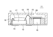
- FIG. 1 is a cross-sectional view showing a conventional microphone having a general structure.
- the microphone 11 is obtained by mounting an acoustic sensor 15 and a signal processing circuit 17 in a package including a cover 12 and a circuit board 13.
- the acoustic sensor 15 and the signal processing circuit 17 are mounted side by side on the upper surface of the circuit board 13.
- the signal processing circuit 17 is covered with a sealing resin 21.
- the acoustic sensor 15 and the signal processing circuit 17 are electrically connected by a bonding wire 18, and the signal processing circuit 17 is further connected to the in-board wiring 14 of the circuit board 13 by a bonding wire 19.
- the lower surface of the circuit board 13 is mounted on the printed wiring board and is in close contact with the printed wiring board. Therefore, a sound introduction hole 20 for introducing acoustic vibration into the package is opened on the upper surface of the cover 12.
- the lower surface of the acoustic sensor 15 is bonded to the circuit board 13, and the lower surface of the back chamber 16 is closed with the circuit board 13.
- the capacitance type microphone there is a correlation between the sensitivity of the microphone and the volume of the back chamber, and the sensitivity of the microphone decreases as the volume of the back chamber decreases.
- the sound introduction hole 20 is provided in the cover 12, and the space between the acoustic sensor 15 and the circuit board 13 is used as the back chamber 16. Therefore, the volume of the back chamber 16 cannot be increased, and the sensitivity of the microphone 11 is increased. Difficult to do.
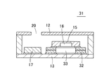
- FIG. 1 A microphone disclosed in Patent Document 1 is shown in FIG.
- the signal processing circuit 17 is mounted on the upper surface of the circuit board 13.
- a spacer 32 is fixed on the upper surface of the circuit board 13, and the acoustic sensor 15 is mounted on the upper surface of the spacer 32.
- the spacer 32 has a through hole 33 penetrating vertically.
- An electrode pad is provided on the lower surface of the acoustic sensor 15, and the acoustic sensor 15 is electrically connected to the circuit board 13 through a spacer 32.
- the sound introduction hole 20 is opened in the cover 12.
- the through hole 33 of the spacer 32 is continuous with the back chamber 16 of the acoustic sensor 15, the space under the diaphragm is widened. Therefore, the volume of the back chamber 16 of the acoustic sensor 15 can be substantially enlarged, and the sensitivity of the microphone 31 can be improved.
- a method of reducing the height of such a microphone As a method of reducing the height of such a microphone, a method of reducing the height of the acoustic sensor by polishing and thinning the substrate portion of the acoustic sensor in the acoustic sensor manufacturing process can be considered.
- a plurality of acoustic sensors are fabricated on the wafer at a time. Therefore, if the substrate portion of the acoustic sensor is to be thinned, the wafer is polished and thinned during the manufacturing process of the acoustic sensor.
- the wafer is usually thin and has a large diameter. Therefore, when the wafer is polished and made thinner, the rigidity of the wafer is considerably reduced. As a result, the wafer may be cracked or chipped during the polishing process or subsequent processes, and the yield of the acoustic sensor may be reduced.
- the present invention has been made in view of the technical problems as described above, and an object thereof is to provide a semiconductor device having a structure in which a semiconductor element is mounted on a support member (for example, on a support member).
- An object of the present invention is to provide a manufacturing method capable of reducing the height of a semiconductor element in a microphone having a structure in which an acoustic sensor is mounted, and thus reducing the height of a semiconductor device.
- the method of manufacturing a semiconductor device includes a step of manufacturing a semiconductor element on a semiconductor substrate, a step of bonding a surface of the semiconductor substrate on which the semiconductor element is manufactured to a support member, the semiconductor substrate, And a step of polishing the surface of the semiconductor substrate opposite to the surface on which the semiconductor element is manufactured to reduce the thickness of the semiconductor substrate in a state where the support member is bonded.
- the semiconductor substrate on which the semiconductor element is manufactured and the support member are joined, and then the semiconductor substrate is polished while the two are joined.
- the thickness is reduced. Therefore, the height of the semiconductor element manufactured over the semiconductor substrate can be reduced, and the height of the semiconductor device can be reduced.
- the semiconductor substrate can be polished in a state in which the semiconductor substrate is bonded to the supporting member to increase the rigidity of the semiconductor substrate. Therefore, the semiconductor substrate is less likely to be cracked or chipped during the polishing process or after the polishing process, so that the yield of the semiconductor elements can be improved and the semiconductor device can be substantially reduced in height. Can be.
- the support member is mounted on a circuit board, and the support member is electrically conductive to electrically connect the semiconductor element and the circuit board.
- the body may penetrate vertically. According to such an embodiment, the height of the semiconductor device can be reduced as compared with the case where the bonding wire is used to connect the semiconductor element to the circuit board.
- the semiconductor substrate is a wafer on which a plurality of the semiconductor elements are manufactured, and the plurality of support members are formed of different wafers. Also good.
- a plurality of semiconductor elements and support members can be manufactured at a time, and the manufacturing efficiency of the semiconductor device is improved.
- a thin and large-diameter wafer is used as the semiconductor substrate and the supporting member.
- the wafer is less likely to be broken or chipped by polishing according to the method of the present invention. Therefore, the usefulness of the present invention is further increased.
- the microphone manufacturing method includes a step of producing an acoustic sensor on a semiconductor substrate, a step of producing a support member by forming a cavity in a plate, and a surface of the semiconductor substrate on which the acoustic sensor is produced. And bonding the surface of the semiconductor substrate to the support member, and polishing the surface of the semiconductor substrate opposite to the surface on which the acoustic sensor has been fabricated. And a step of mounting the acoustic sensor, the support member and the signal processing circuit formed on the semiconductor substrate after the polishing process in a package.
- the semiconductor substrate on which the acoustic sensor is manufactured and the plate serving as the support member are joined, and then the semiconductor substrate is polished while the two are joined.
- the thickness of the semiconductor substrate is reduced. Therefore, the height of the acoustic sensor manufactured on the semiconductor substrate can be reduced, and the height of the microphone can be reduced.
- the semiconductor substrate can be polished in a state in which the semiconductor substrate is bonded to the supporting member to increase the rigidity of the semiconductor substrate. Therefore, it becomes difficult for cracks and chips to occur in the semiconductor substrate during the polishing process or after the polishing process, which can improve the yield of the acoustic sensor and substantially reduce the height of the microphone. it can.
- the cavity may be a space for housing the signal processing circuit. According to such an embodiment, by placing the signal processing circuit in the cavity of the support member, the plane area of the microphone can be reduced, and the microphone can be reduced in size.
- the cavity may be a space communicating with the back chamber of the acoustic sensor.
- the volume of the back chamber of the acoustic sensor can be substantially expanded, and the sensitivity of the acoustic sensor is improved.
- a conductor for electrically connecting the acoustic sensor and an electrode pad provided on the package penetrates the support member vertically. Also good. According to such an embodiment, the height of the microphone can be reduced as compared with the case where a bonding wire is used to connect the acoustic sensor to the package.
- a microphone manufacturing method is characterized in that the plate is a semiconductor substrate. If a semiconductor substrate is used as the plate of the support member, the support member can be processed using MEMS technology or photolithography in the same manner as the acoustic sensor.
- the semiconductor substrate is a wafer on which a plurality of the acoustic sensors are manufactured
- the plate is a wafer on which a plurality of the supporting members are manufactured. It is characterized by being.
- a plurality of acoustic sensors and support members can be produced at a time, and the manufacturing efficiency of the microphone is improved.
- a thin and large-diameter wafer is used as the semiconductor substrate or plate, but even in that case, according to the method of the present invention, the wafer is not easily cracked or chipped by polishing. Therefore, the usefulness of the present invention is further increased.
- the means for solving the above-described problems in the present invention has a feature in which the above-described constituent elements are appropriately combined, and the present invention enables many variations by combining such constituent elements. .
- FIG. 1 is a cross-sectional view showing a microphone having a general structure.
- FIG. 2 is a cross-sectional view of the microphone disclosed in Patent Document 1.
- FIG. 3 is a cross-sectional view showing the structure of the microphone according to Embodiment 1 of the present invention.
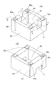
- FIG. 4A is a perspective view of an interposer used in the microphone of the first embodiment.
- FIG. 4B is a perspective view of the interposer drawn upside down.
- FIG. 5A is a cross-sectional view taken along line XX of FIG.
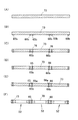
- FIG. 5B is a cross-sectional view taken along line YY of FIG. 6 (A) to 6 (F) are cross-sectional views for explaining the manufacturing process of the interposer.
- FIG. 5A is a cross-sectional view taken along line XX of FIG.
- FIG. 5B is a cross-sectional view taken along line YY of FIG. 6 (A) to 6 (F) are cross-sectional views for explaining the
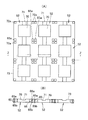
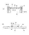
- FIG. 7A is a plan view showing a plurality of microphones integrally manufactured by the steps of FIGS. 6A to 6F.
- FIG. 7B is a cross-sectional view taken along line ZZ in FIG.
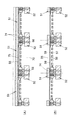
- FIG. 8A is a cross-sectional view illustrating a state in which a plurality of acoustic sensors are manufactured at a time, which is a part of the manufacturing process of the microphone.
- FIG. 8B is a cross-sectional view showing a state in which the acoustic sensor of FIG. 8A is joined and integrated by being turned upside down on the interposer of FIG.
- FIG. 9A is a cross-sectional view illustrating a process of polishing and thinning the Si wafer of the acoustic sensor.
- FIG. 9A is a cross-sectional view illustrating a process of polishing and thinning the Si wafer of the acoustic sensor.
- FIG. 9B is a cross-sectional view showing a state where the front chamber is opened in the Si wafer of the acoustic sensor and the sacrificial layer is removed by etching.
- FIG. 10A is a cross-sectional view showing one acoustic sensor and an interposer divided by dicing.
- FIG. 10B is a cross-sectional view illustrating a process of mounting the signal processing circuit on the upper surface of the circuit board.
- FIG. 11A is a cross-sectional view showing a state where the acoustic sensor and the interposer are mounted on the circuit board so as to cover the signal processing circuit.
- FIG. 11B is a cross-sectional view illustrating a state where a cover is attached to the upper surface of the circuit board.
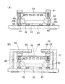
- FIG. 12 is a cross-sectional view showing the structure of a microphone according to Embodiment 2 of the present invention.
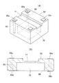
- FIGS. 13A and 13B are a perspective view and a cross-sectional view of an interposer used in the microphone of the second embodiment.
- FIG. 14 is a cross-sectional view showing the structure of a microphone according to Embodiment 3 of the present invention.
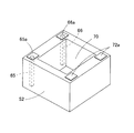
- FIG. 15 is a perspective view of an interposer used in the microphone of the third embodiment.
- FIG. 16A is a perspective view showing a different form of interposer.
- FIG. 16B is a cross-sectional view thereof.
- a microphone will be described as an example of a semiconductor device.
- an acoustic sensor is used as a semiconductor element.
- the present invention is not limited to the following embodiments, and various design changes can be made without departing from the gist of the present invention.
- FIG. 3 is a cross-sectional view illustrating the structure of the microphone 41 according to the first embodiment.
- 4A is a perspective view of an interposer 52 (that is, a supporting member) used in the microphone 41
- FIG. 4B is a perspective view showing the interposer 52 in a vertically inverted state.
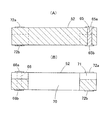
- 5A and 5B are cross-sectional views of the interposer 52.
- FIG. 5A shows a cross-sectional view taken along line XX of FIG. 4A, and FIG. A cross section along line YY of A) is shown.
- a package is formed by the cover 42 and the circuit board 43.
- an acoustic sensor 51 that is, a semiconductor element
- an interposer 52 that is, a semiconductor element
- a signal processing circuit 53 is housed.
- a plurality of upper surface electrode pads 44 for bonding the interposer 52 and the signal processing circuit 53 are provided on the upper surface of the circuit board 43 constituting a part of the package.
- the lower surface of the circuit board 43 is provided with a plurality of lower surface electrode pads 45 for connecting the microphone 41 to the printed wiring board or the like when the microphone 41 is mounted on the printed wiring board or the like.
- the cover 42 has a box shape with an open bottom surface, and an electromagnetic shield film 47 made of a metal plating film is formed on the inner surface of a cover body 46 made of an insulating material (for example, plastic).
- the cover 42 has at least one sound introduction hole 48 for introducing acoustic vibration into the package.
- the cover main body 46 may be made of metal.
- the cover main body 46 has a function of electromagnetic shielding, so that it is not necessary to provide the electromagnetic shielding film 47 separately.
- the acoustic sensor 51 is a capacitive element manufactured using MEMS technology. As shown in FIG. 3, the acoustic sensor 51 is entirely held by a silicon substrate 54 (semiconductor substrate). A front chamber 55 is opened in the silicon substrate 54 so as to penetrate vertically. A thin film diaphragm 56 is provided on the lower surface of the silicon substrate 54 so as to cover the lower surface opening of the front chamber 55.
- the diaphragm 56 is made of conductive polysilicon. Therefore, the diaphragm 56 itself is a movable electrode plate.
- the diaphragm 56 is stretched like a film on the lower surface of the silicon substrate 54 by supporting a plurality of locations on the outer peripheral edge with anchors (not shown). Between the anchors, a vent hole (narrow gap) is formed between the outer peripheral edge of the diaphragm 56 and the lower surface of the silicon substrate 54.
- a back plate 57 is provided below the diaphragm 56 so as to form an air gap 58 (gap) between the diaphragm 56 and the outer periphery of the back plate 57 is fixed to the lower surface of the silicon substrate 54. ing.
- a fixed electrode plate 59 is provided on the upper surface of the back plate 57 so as to face the diaphragm 56.
- the back plate 57 is made of insulating SiN, and the fixed electrode plate 59 is made of conductive polysilicon.
- acoustic holes 60 acoustic holes
- a lead wire 61 extends from the end of the diaphragm 56.
- An electrode portion 62 embedded in the back plate 57 is electrically connected to the end portion of the lead wiring 61.
- a lead wiring 63 extends from the end of the fixed electrode plate 59.
- An electrode portion 64 embedded in the back plate 57 is electrically connected to the end portion of the lead wiring 63.
- the lower surface of the electrode portion 62 is exposed at any one of the four corners of the lower surface of the acoustic sensor 51, and a bump 67 is provided on the lower surface of the electrode portion 62.
- the lower surface of the electrode part 64 is exposed at another corner among the four corners of the lower surface of the acoustic sensor 51, and a bump 67 is provided on the lower surface of the electrode part 64.
- dummy electrodes are provided at the corners where the electrode portions 62 and 64 are not provided.
- the dummy electrode is an electrode for mechanically fixing the lower surface of the acoustic sensor 51 with solder or the like, and has no electrical function.
- the dummy electrode is also provided with bumps.
- the interposer 52 has a structure as shown in FIGS. 4A, 4B, 5A, and 5B.
- the interposer 52 is formed in a rectangular tube shape by an insulating material, particularly a semiconductor substrate, and a cavity 70 for accommodating the signal processing circuit 53 vertically penetrates the interposer 52. Further, a ventilation notch 71 (that is, an acoustic transmission path) is formed in the upper portion of the wall surface of the interposer 52.
- the interposer 52 has a structure for electrically connecting the acoustic sensor 51 and the circuit board 43. That is, a through electrode 65 (conductor) is embedded in one of the four corners of the interposer 52, a pad portion 65 a electrically connected to the through electrode 65 is provided on the upper surface of the interposer 52, and the through electrode 65 is provided on the lower surface. And a pad portion 65b that is electrically connected to each other.
- a penetrating electrode 66 (conductor) is embedded in another part of the four corners of the interposer 52, a pad portion 66a electrically connected to the penetrating electrode 66 is provided on the upper surface of the interposer 52, and the penetrating electrode 66 is provided on the lower surface.
- the dummy electrode 72a is provided on the upper surface of the interposer 52, and the dummy electrode 72b is provided on the lower surface.
- the dummy electrodes 72a and 72b are electrodes for mechanically connecting and fixing the interposer 52, and the upper dummy electrode 72a and the lower dummy electrode 72b are not electrically connected.
- the ventilation notch 71 is formed in the upper part of the wall surface.
- the ventilation notch 71 may be provided in the lower part of the wall surface of the interposer 52.
- a ventilation opening may be opened in the shape of a window on the wall surface of the interposer 52 as an acoustic transmission path.
- an acoustic transmission passage such as a ventilation notch or a ventilation opening needs to have a passage cross-sectional area that can transmit a dynamic pressure change due to acoustic vibration.
- the signal processing circuit 53 is a circuit for amplifying the acoustic detection signal output from the acoustic sensor 51, further converting the signal into a digital signal, and outputting the digital signal.
- an electrode unit 69 for inputting a signal from the acoustic sensor 51 and an electrode unit 69 for outputting a signal-processed signal are provided.
- the microphone 41 is assembled as follows.
- the acoustic sensor 51 is placed on the interposer 52, the bump 67 provided on the lower surface of the electrode portion 62 is bonded to the upper surface (pad portion 65 a) of the through electrode 65, and the bump 67 provided on the lower surface of the electrode portion 64 is formed.
- the through electrode 66 is bonded to the upper surface (pad portion 66a).
- the bump 67 of the dummy electrode provided on the lower surface of the acoustic sensor 51 is bonded to the dummy electrode 72 a on the upper surface of the interposer 52.
- the acoustic sensor 51 is mechanically fixed to the upper surface of the interposer 52 by the four bumps 67.
- the electrode parts 62 and 64 of the acoustic sensor 51 are electrically connected to the lower surface (pad parts 65b and 66b) of the interposer 52 through the through electrodes 65 and 66, respectively.
- the pad portions 65b and 66b and the dummy electrode 72b provided on the lower surface of the interposer 52 are joined to the upper electrode pad 44 of the circuit board 43 by a conductive material 68 such as solder or conductive adhesive.
- the electrode portion 69 of the signal processing circuit 53 is also bonded to the upper electrode pad 44 of the circuit board 43 by a conductive material 68 such as solder or a conductive adhesive.
- the cover 42 is overlaid on the upper surface of the circuit board 43 so as to cover the acoustic sensor 51, the interposer 52 and the signal processing circuit 53 mounted on the upper surface of the circuit board 43.
- the sound introduction hole 48 of the cover 42 is disposed so as to face the front chamber 55 of the acoustic sensor 51.
- the entire upper surface of the acoustic sensor 51 (the upper surface of the silicon substrate 54) is sealed by adhering the entire circumference to the inner surface of the cover 42 using an adhesive resin 50.
- the lower surface of the cover 42 is bonded to the upper surface of the circuit board 43 with a conductive adhesive, and the electromagnetic shield film 47 is electrically connected to the ground electrode of the circuit board 43.
- the acoustic vibration When acoustic vibration enters the microphone 41 from the sound introduction hole 48, the acoustic vibration is guided into the front chamber 55 of the acoustic sensor 51. Since the acoustic vibration causes the diaphragm 56 to vibrate, the capacitance of the capacitor formed by the diaphragm 56 and the fixed electrode plate 59 is changed, and this change in capacitance is output from the electrode portions 62 and 64 as an acoustic detection signal. The The acoustic detection signal output from the acoustic sensor 51 is transmitted to the upper electrode pad 44 through the through electrodes 65 and 66.
- the upper surface electrode pad 44 to which the pad portions 65b and 66b of the through electrodes 65 and 66 are joined is an electrode for signal input of the signal processing circuit 53 by a wiring pattern (not shown) provided on the upper surface or inside of the circuit board 43.
- the portion 69 is electrically connected to the joined upper electrode pad 44. Therefore, the acoustic detection signal of the acoustic sensor 51 is input into the signal processing circuit 53 from the electrode portion 69 for signal input.
- the upper electrode pad 44 to which the signal output electrode portion 69 is bonded is connected to the lower electrode pad 45 of the circuit board 43 by a wiring structure (not shown) provided inside the circuit board 43. Therefore, the output signal processed by the signal processing circuit 53 is output from the lower surface electrode pad 45 of the circuit board 43 to the outside.
- the electrical connection form between the acoustic sensor 51 and the signal processing circuit 53, the number of through electrodes in the interposer 52, and the like vary depending on the configuration of the acoustic sensor 51 and the signal processing circuit 53, and thus the above description represents an example. .
- the acoustic sensor 51 having such a configuration, the following operational effects can be obtained.
- a bonding wire see, for example, FIG. 1
- the bonding wire may be broken due to vibration or the like.
- the bonding wire is slackened and wired, the wire may come into contact with the acoustic sensor or the electrode pad of the signal processing circuit. For this reason, the bonding wire is laid loosely upward.
- the height of the package is required to be high enough to accommodate the bonding wire that protrudes upward, and the height of the microphone is increased accordingly.
- the acoustic sensor 51 of this embodiment the acoustic sensor 51 and the signal processing circuit 53 are connected through the through electrodes 65 and 66 provided in the interposer 52. Therefore, it is not necessary to consider the slackness of the bonding wire as in the case of connecting using the bonding wire, and the height of the acoustic sensor 51 is not increased unnecessarily.
- the acoustic sensor 51 and the signal processing circuit 53 are arranged above and below, an area for mounting the signal processing circuit 53 is not required separately from the area for mounting the acoustic sensor 51, as in the conventional case.
- the plane area of the microphone 41 can be significantly reduced. Therefore, even when the size of the acoustic sensor 51 and the signal processing circuit 53 cannot be reduced, the microphone 41 can be reduced in size.
- a space surrounded by the silicon substrate 54 between the sound introduction hole 48 and the diaphragm 56 is a front chamber 55.
- the space on the lower surface side of the diaphragm 56 becomes the back chamber of the acoustic sensor 51.
- the acoustic vibration after passing through the diaphragm 56 can pass through the acoustic hole 60 and spread into the cavity 70 in the interposer 52, and further pass through the ventilation notch 71 and spread into the package internal space 49.
- the package internal space 49 refers to a space outside the acoustic sensor 51 and the interposer 52 in the space surrounded by the cover 42 and the circuit board 43.
- a space obtained by combining the space below the diaphragm 56 in the acoustic sensor 51, the cavity 70 in the interposer 52, and the package internal space 49 is a substantial back chamber. That is, in the microphone 41, almost all the spaces in the package except the front chamber 55 become the back chamber.
- the sensitivity of the acoustic sensor 51 increases as the back chamber volume increases.
- most of the space in the package can be used as a back chamber, so that the sensitivity of the acoustic sensor 51 can be improved.
- the electromagnetic shield film 47 is formed on the inner surface of the cover 42 (the electromagnetic shield film may also be provided inside the circuit board 43).
- the signal processing circuit 53 can be blocked from external noise, and the S / N ratio of the microphone 41 can be improved.
- FIG. 7A is a plan view showing a plurality of interposers 52 that are integrally manufactured as a result.
- FIG. 7B shows a cross section taken along line ZZ in FIG.
- the plurality of interposers 52 are produced as follows.
- FIG. 6A shows an insulating Si wafer 73 for producing a plurality of interposers 52 at one time.
- a metal thin film is formed on the lower surface of the Si wafer 73, and the metal thin film is patterned by photolithography or the like.
- pad portions 65b, 66b and 72b are formed at predetermined positions on the lower surface of the Si wafer 73, respectively.
- through holes 76 are opened on the pad portions 65b and 66b by etching the Si wafer 73.
- a metal material is filled into the through hole 76 by plating or the like, and through electrodes 65 and 66 are formed in the through hole 76 as shown in FIG.
- the through electrode 65 is formed on the pad portion 65b and is electrically connected to the pad portion 65b.
- the through electrode 66 is formed on the pad portion 66b and is electrically connected to the pad portion 66b.
- a metal thin film is formed on the upper surface of the Si wafer 73, and the metal thin film is patterned by photolithography or the like. As a result, as shown in FIG. 6E, a pad portion 65 b that is electrically connected to the through electrode 65 is formed on the through electrode 65, and a pad portion 66 b that is electrically connected to the through electrode 66 is formed on the through electrode 66. It is formed.
- a dummy electrode 72 a is formed at a position facing the dummy electrode 72 b on the upper surface of the Si wafer 73. Thereafter, by etching the central portion of the region surrounded by the pair of pad portions 65a and 66a and the dummy electrode 72a, the cavity 70 penetrating vertically is opened as shown in FIG. Finally, the upper surface of the Si wafer 73 is etched into a groove shape to form a ventilation notch 71, and a plurality of interposers 52 are integrated. Thus, as shown in FIGS. 7A and 7B, a plurality of interposers 52 are produced.
- FIG. 8A is a cross-sectional view showing a plurality of acoustic sensors 51 manufactured integrally.
- a polysilicon diaphragm 56 is provided for each region to be the acoustic sensor 51.
- a sacrificial layer 75 is formed on the diaphragm 56, and a fixed electrode plate 59 and a back plate 57 are provided on the upper surface of the sacrificial layer 75.
- electrode portions 62 and 64 and dummy electrodes are provided at each corner of a region to be each acoustic sensor 51.
- the acoustic sensor 51 manufactured as shown in FIG. 8A is turned upside down and overlaid on the upper surface of the interposer 52 in FIG. 65a, the electrode part 64 and the pad part 66a, and the dummy electrode and the dummy electrode 72a are joined.
- the Si wafer 74 having a plurality of acoustic sensors 51 and the Si wafer 73 having a plurality of interposers 52 are bonded together.
- the upper surface of the acoustic sensor 51 is polished to reduce the thickness of the Si wafer 74. Since the wafer is thin and has a substantially disk shape with a large diameter, the rigidity is not so high. Therefore, if the Si wafer 74 on which the acoustic sensor 51 is formed is polished alone to reduce the thickness of the Si wafer 74, the Si wafer 74 is cracked or chipped during the polishing process or in the subsequent process, and the acoustic sensor. 51 yield decreases. However, in the manufacturing method described here, since the two Si wafers, that is, the Si wafer 73 and the Si wafer 74 are bonded together, the rigidity of the wafer can be increased. Therefore, by polishing after bonding the Si wafer 74 and the Si wafer 73, it is possible to polish the Si wafer 74 with increased rigidity, so that the Si wafer 74 can be polished easily and with a high yield. become.
- the sacrificial layer 75 of the acoustic sensor 51 is removed by etching, and an air gap 58 is formed between the diaphragm 56 and the fixed electrode plate 59.
- the diaphragm 56 is formed into a vibrating film.
- the Si wafers 74 and 73 are diced along a cutting line indicated by a one-dot chain line in FIG.
- the acoustic sensor 51 and the interposer 52 are separated one by one while being joined up and down.
- the signal processing circuit 53 is flip-chip mounted on the upper surface of the circuit board 43, and the electrode portion 69 of the signal processing circuit 53 is bonded to the upper electrode pad 44 of the circuit board 43 by the conductive material 68.
- a signal processing circuit 53 thus mounted on the circuit board 43 is shown in FIG.
- the integrated interposer 52 and the acoustic sensor 51 are overlaid on the circuit board 43 to cover the signal processing circuit 53, and the signal processing circuit 53 is placed in the cavity 70 of the interposer 52. Pay. At this time, the pad portions 65 b and 66 b of the interposer 52 and the dummy electrode 72 b are bonded to the upper surface electrode pad 44 of the circuit board 43 by the conductive material 68.
- the cover 42 is overlaid on the circuit board 43 so as to cover the acoustic sensor 51, the interposer 52 and the signal processing circuit 53.
- a sound introduction hole 48 is opened in advance in the cover 42, and the sound introduction hole 48 overlaps the upper surface opening of the front chamber 55 when the cover 42 is overlaid on the circuit board 43.
- the lower surface of the cover 42 is bonded to the circuit board 43 with a conductive adhesive.
- the upper surface of the acoustic sensor 51 is adhered to the inner surface of the cover 42 by the adhesive resin 50, and the space between the entire upper surface of the acoustic sensor 51 and the entire periphery of the sound introduction hole 48 in the inner surface of the cover 42 is sealed.
- the acoustic vibration entered from the introduction hole 48 is prevented from leaking from the gap between the acoustic sensor 51 and the cover 42.
- the Si wafer 74 is less likely to be cracked or chipped when the Si wafer 74 is polished, so that the yield in the manufacturing process of the microphone 41 is improved. Further, since the Si wafer 74 is hardly cracked or chipped, the thickness of the Si wafer 74 can be reduced by polishing, and the height of the acoustic sensor 51 can be reduced. If the height of the acoustic sensor 51 can be reduced, the cover 42 having a low height can be used, and the microphone 41 can be reduced in height and size.
- FIG. 12 is a cross-sectional view showing a microphone 81 according to Embodiment 2 of the present invention.
- the microphone 81 is different from the microphone 41 of the first embodiment only in the shape of the interposer 52. Therefore, in the microphone 81 according to the second embodiment, descriptions other than the interposer 52 are omitted.
- the cavity 70 for accommodating the signal processing circuit 53 has a box shape with an open bottom surface, and the top surface is It is blocked.
- a ventilation notch 71 having one or more grooves is provided on the upper surface of the interposer 52.
- the space (back chamber) under the diaphragm 56 of the acoustic sensor 51 communicates with the package internal space 49 through the ventilation notch 71 without passing through the cavity 70 for housing the signal processing circuit 53. Yes. Therefore, the volume of the back chamber can be substantially increased, and the sensitivity of the microphone 81 can be improved.
- the cavity 70 of the interposer 52 is a space for accommodating the signal processing circuit 53.
- the acoustic sensor 51 and the signal processing circuit 53 arranged above and below are partitioned by the interposer 52, a short circuit accident between the acoustic sensor 51 and the signal processing circuit 53 can be prevented.
- the signal processing circuit 53 is covered by the interposer 52, the signal processing circuit 53 can be protected from moisture and dust that have entered from the sound introduction hole 48.
- Such a microphone 81 of the second embodiment can also be manufactured in the same manner as the manufacturing method described in the first embodiment, and the microphone 81 can be reduced in height.
- FIG. 14 is a sectional view showing a microphone 82 according to Embodiment 3 of the present invention.
- the signal processing circuit 53 is not placed inside the interposer 52.
- the signal processing circuit 53 is mounted next to the interposer 52 on the upper surface of the circuit board 43. Therefore, in the microphone 82, the cavity 70 in the interposer 52 communicates with the back chamber of the acoustic sensor 51 and functions to increase the volume of the back chamber.
- the microphone 82 according to the third embodiment can be manufactured in the same manner as the manufacturing method described in the first embodiment, and the microphone 82 can be reduced in height.
- the interposer 52 does not necessarily have an acoustic transmission path such as the ventilation notch 71.
- An interposer 52 having no ventilation notch 71 as shown in FIG. 15 can also be used.
- the back chamber is expanded only to the cavity 70 in the interposer 52, and the package internal space 49 cannot be used as the back chamber.
- the interposer 52 can have various structures other than the structures described in the first and second embodiments.
- FIG. 16A and FIG. 16B show still another embodiment.
- the extended electrode portion 83a extends from the pad portion 65a along the upper surface of the interposer 52
- the extended electrode portion 83b extends from the pad portion 65b along the lower surface of the interposer 52
- the distal end portion of the extended electrode portion 83a is connected by a through electrode 65.
- the extended electrode portion 84a extends from the pad portion 66a along the upper surface of the interposer 52
- the extended electrode portion 84b extends from the pad portion 66b along the lower surface of the interposer 52, and extends from the distal end portion of the extended electrode portion 84a.
- the tip portions of the electrode portions 84 b are connected by the through electrode 66.
- the through electrodes 65 and 66 can be provided at arbitrary positions.
Landscapes
- Engineering & Computer Science (AREA)
- Manufacturing & Machinery (AREA)
- Physics & Mathematics (AREA)
- Acoustics & Sound (AREA)
- Signal Processing (AREA)
- Microelectronics & Electronic Packaging (AREA)
- Pressure Sensors (AREA)
- Electrostatic, Electromagnetic, Magneto- Strictive, And Variable-Resistance Transducers (AREA)
- Micromachines (AREA)
- Mechanical Treatment Of Semiconductor (AREA)
Abstract
Siウエハ73の上に複数個の音響センサ51を設ける。Siウエハ74を用いて空洞70や貫通電極65、66などを有する複数個のインターポーザ52を一体に形成する。複数個の音響センサ51の、Siウエハ73と反対側の面を複数個のインターポーザ52に接合一体化する。この後、音響センサ51とインターポーザ52が接合一体化された状態において、音響センサ51のSiウエハ73を研磨してSiウエハ73の厚みを薄くする。この後、接合されたままで1個1個に分割された単体の音響センサ51及びSiウエハ73を、信号処理回路とともにパッケージ内に実装する。
Description
本発明は半導体装置の製造方法に関する。また、本発明は、音響センサをパッケージ内に実装したマイクロフォンの製造方法に関する。
(一般的なマイクロフォン)
図1は、従来の一般的な構造のマイクロフォンを示す断面図である。このマイクロフォン11は、カバー12と回路基板13からなるパッケージ内に音響センサ15と信号処理回路17を実装したものである。音響センサ15と信号処理回路17は、回路基板13の上面に横に並べた状態で実装されている。信号処理回路17は、封止樹脂21によって覆われている。音響センサ15と信号処理回路17は、ボンディングワイヤ18によって電気的に接続されており、さらに信号処理回路17は、ボンディングワイヤ19によって回路基板13の基板内配線14に接続されている。
図1は、従来の一般的な構造のマイクロフォンを示す断面図である。このマイクロフォン11は、カバー12と回路基板13からなるパッケージ内に音響センサ15と信号処理回路17を実装したものである。音響センサ15と信号処理回路17は、回路基板13の上面に横に並べた状態で実装されている。信号処理回路17は、封止樹脂21によって覆われている。音響センサ15と信号処理回路17は、ボンディングワイヤ18によって電気的に接続されており、さらに信号処理回路17は、ボンディングワイヤ19によって回路基板13の基板内配線14に接続されている。
通常、回路基板13の下面はプリント配線基板に実装され、プリント配線基板に密着する。そのため、パッケージ内に音響振動を導き入れるための音導入孔20はカバー12の上面に開口されている。音響センサ15の下面は回路基板13に接着されており、バックチャンバ16の下面は回路基板13で塞がれている。
静電容量型のマイクロフォンでは、マイクロフォンの感度とバックチャンバの容積との間には相関があり、バックチャンバの容積が小さくなるとマイクロフォンの感度が低下する。このマイクロフォン11では、カバー12に音導入孔20を設け、音響センサ15と回路基板13の間の空間をバックチャンバ16としているので、バックチャンバ16の容積を大きくできず、マイクロフォン11の感度を高くすることが困難である。
(特許文献1のマイクロフォン)
特許文献1に開示されているマイクロフォンを図2に示す。特許文献1のマイクロフォン31では、回路基板13の上面に信号処理回路17を実装している。信号処理回路17に隣接する位置において、回路基板13の上面にはスペーサ32が固定されており、さらにスペーサ32の上面に音響センサ15が実装されている。スペーサ32には、上下に貫通する貫通孔33が開口されている。音響センサ15の下面には電極パッドが設けられ、音響センサ15は、スペーサ32を介して回路基板13に電気的に接続されている。音導入孔20は、カバー12に開口されている。
特許文献1に開示されているマイクロフォンを図2に示す。特許文献1のマイクロフォン31では、回路基板13の上面に信号処理回路17を実装している。信号処理回路17に隣接する位置において、回路基板13の上面にはスペーサ32が固定されており、さらにスペーサ32の上面に音響センサ15が実装されている。スペーサ32には、上下に貫通する貫通孔33が開口されている。音響センサ15の下面には電極パッドが設けられ、音響センサ15は、スペーサ32を介して回路基板13に電気的に接続されている。音導入孔20は、カバー12に開口されている。
このマイクロフォン31では、スペーサ32の貫通孔33を音響センサ15のバックチャンバ16と連続させているので、ダイアフラムの下の空間が広くなる。よって、音響センサ15のバックチャンバ16の容積を実質的に拡大することができ、マイクロフォン31の感度を向上させられる。
しかし、このような構造では、回路基板13の上面にスペーサ32を実装し、さらにスペーサ32の上に音響センサ15を実装しているので、マイクロフォン31の高さが高くなる不具合がある。
このようなマイクロフォンの高さを低くする方法としては、音響センサの製造工程において、音響センサの基板部分を研磨して薄くし、音響センサの高さを小さくする方法が考えられる。しかし、音響センサの製造工程では、複数個の音響センサがウエハ上に一度に作製される。そのため、音響センサの基板部分を薄くしようとすれば、音響センサの製造工程中においてウエハを研磨して薄くすることになる。
ウエハは、通常は薄くて大口径のものが用いられる。そのため、ウエハを研磨してさらに薄くすると、ウエハの剛性がかなり小さくなる。その結果、研磨工程もしくはその後の工程でウエハに割れや欠けが発生し、音響センサの歩留まりが低下するおそれがある。
本発明は、上記のような技術的課題に鑑みてなされたものであって、その目的とするところは、支持部材の上に半導体素子を実装した構造の半導体装置(たとえば、支持部材の上に音響センサを実装した構造のマイクロフォン)において、半導体素子の高さを小さくでき、ひいては半導体装置を低背化することのできる製造方法を提供することにある。
本発明に係る半導体装置の製造方法は、半導体基板に半導体素子を作製する工程と、前記半導体基板の前記半導体素子を作製された側の面を支持部材に接合させる工程と、前記半導体基板と前記支持部材が接合された状態において、前記半導体基板の前記半導体素子を作製された面と反対側の面を研磨して前記半導体基板の厚みを薄くする工程とを備えたことを特徴としている。
本発明に係る半導体装置の製造方法にあっては、半導体素子を作製された半導体基板と支持部材とを接合させた後、両者を接合させた状態のままで半導体基板を研磨して半導体基板の厚みを薄くしている。よって、半導体基板に作製された半導体素子の高さを低くすることができ、半導体装置の低背化を図ることができる。さらに、半導体基板を支持部材と貼り合わせて半導体基板の剛性を高めた状態で半導体基板を研磨することができる。よって、研磨の工程中において、あるいは研磨の後の工程において、半導体基板に割れや欠けが発生しにくくなり、半導体素子の歩留まりを向上させることができるとともに実質的に半導体装置の低背化を可能にできる。
本発明のある実施態様による半導体装置の製造方法においては、前記支持部材は、回路基板上に実装され、前記支持部材には、前記半導体素子と前記回路基板とを電気的に導通させるための導電体が上下に貫通していてもよい。かかる実施態様によれば、半導体素子を回路基板に接続するためにボンディングワイヤを用いる場合と比較して、半導体装置の高さを小さくすることができる。
本発明の別な実施態様による半導体装置の製造方法においては、前記半導体基板が、複数個の前記半導体素子を作製されたウエハであり、複数個の前記支持部材が別なウエハによって形成されていてもよい。かかる実施態様によれば、複数個の半導体素子及び支持部材を一度に作製することができ、半導体装置の製造効率が向上する。また、この場合には、半導体基板や支持部材として、薄くて大口径のウエハを用いることになるが、その場合でも、本発明の方法によれば研磨によってウエハに割れや欠けが生じにくくなる。よって、本発明の有用性がより高くなる。
本発明に係るマイクロフォンの製造方法は、半導体基板に音響センサを作製する工程と、プレートに空洞を形成して支持部材を作製する工程と、前記半導体基板の前記音響センサを作製された側の面を前記支持部材に接合させる工程と、前記半導体基板と前記支持部材が接合された状態において、前記半導体基板の前記音響センサを作製された面と反対側の面を研磨して前記半導体基板の厚みを薄くする工程と、研磨処理後の前記半導体基板に形成された前記音響センサ及び前記支持部材と信号処理回路とをパッケージ内に実装する工程とを備えたことを特徴としている。
本発明に係るマイクロフォンの製造方法にあっては、音響センサを作製された半導体基板と支持部材となったプレートとを接合させた後、両者を接合させた状態のままで半導体基板を研磨して半導体基板の厚みを薄くしている。よって、半導体基板に作製された音響センサの高さを低くすることができ、マイクロフォンの低背化を図ることができる。さらに、半導体基板を支持部材と貼り合わせて半導体基板の剛性を高めた状態で半導体基板を研磨することができる。よって、研磨の工程中において、あるいは研磨の後の工程において、半導体基板に割れや欠けが発生しにくくなり、音響センサの歩留まりを向上させることができるとともに実質的にマイクロフォンの低背化を可能にできる。
本発明のある実施態様によるマイクロフォンの製造方法においては、前記空洞が、前記信号処理回路を納めるための空間であってもよい。かかる実施態様によれば、信号処理回路を支持部材の空洞内に納めることによってマイクロフォンの平面積を小さくでき、マイクロフォンの小型化を図ることができる。
本発明の別な実施態様によるマイクロフォンの製造方法においては、前記空洞が、前記音響センサのバックチャンバと連通した空間であってもよい。かかる実施態様によれば、音響センサのバックチャンバの容積を実質的に拡張することができ、音響センサの感度が向上する。
本発明のさらに別な実施態様によるマイクロフォンの製造方法においては、前記支持部材に、前記音響センサと前記パッケージに設けた電極パッドとを電気的に導通させるための導電体が上下に貫通していてもよい。かかる実施態様によれば、音響センサをパッケージに接続するためにボンディングワイヤを用いる場合と比較して、マイクロフォンの高さを小さくすることができる。
本発明のさらに別な実施態様によるマイクロフォンの製造方法は、前記プレートが、半導体基板であることを特徴としている。支持部材のプレートとして半導体基板を用いれば、音響センサと同じようにMEMS技術やフォトリソグラフィを用いて支持部材を加工することができる。
本発明のさらに別な実施態様によるマイクロフォンの製造方法は、前記半導体基板が、複数個の前記音響センサを作製されたウエハであり、前記プレートが、複数個の前記支持部材を作製されたウエハであることを特徴としている。かかる実施態様によれば、複数個の音響センサ及び支持部材を一度に作製することができ、マイクロフォンの製造効率が向上する。また、この場合には、半導体基板やプレートとして、薄くて大口径のウエハを用いることになるが、その場合でも、本発明の方法によれば研磨によってウエハに割れや欠けが生じにくくなる。よって、本発明の有用性がより高くなる。
なお、本発明における前記課題を解決するための手段は、以上説明した構成要素を適宜組み合せた特徴を有するものであり、本発明はかかる構成要素の組合せによる多くのバリエーションを可能とするものである。
以下、添付図面を参照しながら本発明の好適な実施形態を説明する。以下の実施形態においては、半導体装置の一例としてマイクロフォンについて述べる。このマイクロフォンでは、半導体素子として音響センサが用いられている。但し、本発明は以下の実施形態に限定されるものでなく、本発明の要旨を逸脱しない範囲において種々設計変更することができる。
(第1の実施形態)
以下、図3-図5を参照して本発明の実施形態1によるマイクロフォン(すなわち、半導体装置)を説明する。図3は、実施形態1に係るマイクロフォン41の構造を示す断面図である。また、図4(A)は、マイクロフォン41に用いられているインターポーザ52(すなわち、支持部材)の斜視図、図4(B)は、インターポーザ52を上下反転させた状態で示す斜視図である。図5(A)及び図5(B)はインターポーザ52の断面図であって、図5(A)は図4(A)のX-X線断面を示し、図5(B)は図4(A)のY-Y線断面を示す。
以下、図3-図5を参照して本発明の実施形態1によるマイクロフォン(すなわち、半導体装置)を説明する。図3は、実施形態1に係るマイクロフォン41の構造を示す断面図である。また、図4(A)は、マイクロフォン41に用いられているインターポーザ52(すなわち、支持部材)の斜視図、図4(B)は、インターポーザ52を上下反転させた状態で示す斜視図である。図5(A)及び図5(B)はインターポーザ52の断面図であって、図5(A)は図4(A)のX-X線断面を示し、図5(B)は図4(A)のY-Y線断面を示す。
マイクロフォン41にあっては、カバー42と回路基板43によってパッケージが形成されている。このパッケージ内には、音響センサ51(すなわち、半導体素子)、インターポーザ52および信号処理回路53が納められている。
パッケージの一部を構成する回路基板43の上面には、インターポーザ52や信号処理回路53を接合させるための複数個の上面電極パッド44が設けられている。回路基板43の下面には、マイクロフォン41をプリント配線基板などに実装するときに、マイクロフォン41をプリント配線基板などに接続させるための複数個の下面電極パッド45が設けられている。カバー42は、下面が開口した箱状をしており、絶縁性材料(たとえば、プラスチック)からなるカバー本体46の内面に、金属メッキ膜による電磁シールド膜47が形成されている。また、カバー42にはパッケージ内に音響振動を導き入れるための音導入孔48が少なくとも1箇所に開口されている。
なお、カバー本体46は金属製であってもよく、その場合にはカバー本体46が電磁シールドの機能を有するので、別途電磁シールド膜47を設ける必要はない。
音響センサ51はMEMS技術を利用して作製された静電容量型素子である。図3に示すように、音響センサ51は、全体をシリコン基板54(半導体基板)によって保持されている。シリコン基板54には、上下に貫通するようにしてフロントチャンバ55が開口されている。シリコン基板54の下面には、フロントチャンバ55の下面開口を覆うようにして、薄膜状のダイアフラム56が設けられている。ダイアフラム56は、導電性を有するポリシリコンによって形成されている。したがって、ダイアフラム56は、それ自体が可動電極板となっている。ダイアフラム56は、外周縁の複数箇所をアンカー(図示せず)によって支持されることにより、シリコン基板54の下面で膜状に張られている。アンカー間においては、ダイアフラム56の外周縁とシリコン基板54の下面との間にベントホール(狭い隙間)が形成されている。
ダイアフラム56の下方には、ダイアフラム56との間にエアギャップ58(空隙)を形成するようにして、バックプレート57が設けられており、バックプレート57の外周部はシリコン基板54の下面に固定されている。また、バックプレート57の上面には、ダイアフラム56と対向するようにして固定電極板59が設けられている。バックプレート57は絶縁性のSiNによって形成され、固定電極板59は導電性のポリシリコンによって形成されている。この結果、エアギャップ58を介して対向しているダイアフラム56と固定電極板59によって音響振動検知用のキャパシタが構成されている。
バックプレート57及び固定電極板59のほぼ全体には、ダイアフラム56を振動させた後の音響振動を通過させるためのアコースティックホール60(音響孔)が多数穿孔されている。
ダイアフラム56の端部からは引出配線61が延出されている。引出配線61の端部には、バックプレート57に埋め込まれた電極部62が電気的に接続されている。また、固定電極板59の端部からは引出配線63が延出されている。引出配線63の端部には、バックプレート57に埋め込まれた電極部64が電気的に接続されている。電極部62の下面は、音響センサ51の下面の四隅のうちいずれか1箇所の隅部に露出しており、電極部62の下面にはバンプ67が設けられている。電極部64の下面は、音響センサ51の下面の四隅のうち別な隅部において露出しており、電極部64の下面にはバンプ67が設けられている。音響センサ51の下面の四隅のうち、電極部62、64が設けられていない隅部には、ダミーの電極(図示せず)が設けられている。ダミーの電極とは、音響センサ51の下面をハンダなどで機械的に固定するための電極であって、電気的な働きを有しないものである。ダミーの電極にもバンプが設けられている。
インターポーザ52は、図4(A)、図4(B)、図5(A)及び図5(B)に示すような構造を有している。インターポーザ52は、絶縁性材料、特に半導体基板によって角筒状に形成されており、インターポーザ52内には信号処理回路53を納めるための空洞70が上下に貫通している。また、インターポーザ52の壁面上部には通気用切欠71(すなわち、音響伝達通路)が形成されている。
インターポーザ52は、音響センサ51と回路基板43を電気接続するための構造を備えている。すなわち、インターポーザ52の四隅のうち1箇所には貫通電極65(導電体)が埋め込まれており、インターポーザ52の上面には貫通電極65と導通したパッド部65aが設けられ、下面には貫通電極65と導通したパッド部65bが設けられている。
インターポーザ52の四隅のうち別な箇所には、貫通電極66(導電体)が埋め込まれており、インターポーザ52の上面には貫通電極66と導通したパッド部66aが設けられ、下面には貫通電極66と導通したパッド部66bが設けられている。さらに、インターポーザ52の四隅のうち貫通電極65、66が設けられていない箇所では、インターポーザ52の上面にダミー電極72aが設けられ、下面にダミー電極72bが設けられている。ダミー電極72a、72bは機械的に接続してインターポーザ52を固定するための電極であり、上面のダミー電極72aと下面のダミー電極72bとは電気的には導通していない。
インターポーザ52の四隅のうち別な箇所には、貫通電極66(導電体)が埋め込まれており、インターポーザ52の上面には貫通電極66と導通したパッド部66aが設けられ、下面には貫通電極66と導通したパッド部66bが設けられている。さらに、インターポーザ52の四隅のうち貫通電極65、66が設けられていない箇所では、インターポーザ52の上面にダミー電極72aが設けられ、下面にダミー電極72bが設けられている。ダミー電極72a、72bは機械的に接続してインターポーザ52を固定するための電極であり、上面のダミー電極72aと下面のダミー電極72bとは電気的には導通していない。
なお、図4及び図5のインターポーザ52では、その壁面上部に通気用切欠71が形成されているが、インターポーザ52の壁面下部に通気用切欠71を設けてもよい。また、インターポーザ52の壁面に音響伝達通路として通気用開口を窓状に開口してもよい。ただし、通気用切欠や通気用開口などの音響伝達通路は、音響振動による動的な圧力変化を伝えられるだけの通路断面積を有していることが必要である。
信号処理回路53(ASIC)は、音響センサ51から出力される音響検知信号を増幅し、さらにその信号をデジタル信号に変換して出力するための回路である。信号処理回路53の下面には、音響センサ51からの信号を入力させるための電極部69や信号処理された信号を出力するための電極部69が設けられている。
マイクロフォン41は、つぎのようにして組み立てられている。音響センサ51は、インターポーザ52の上に載置され、電極部62の下面に設けたバンプ67が貫通電極65の上面(パッド部65a)に接合され、電極部64の下面に設けたバンプ67が貫通電極66の上面(パッド部66a)に接合されている。また、音響センサ51の下面に設けられたダミーの電極のバンプ67は、インターポーザ52の上面のダミー電極72aに接合されている。この結果、音響センサ51は4箇所のバンプ67によってインターポーザ52の上面に機械的に固定されている。さらに、音響センサ51の電極部62、64は、それぞれ貫通電極65、66を通じてインターポーザ52の下面(パッド部65b、66b)に導通している。
インターポーザ52の下面に設けられたパッド部65b、66b及びダミー電極72bは、それぞれハンダや導電性接着剤などの導電材料68によって回路基板43の上面電極パッド44に接合される。信号処理回路53の電極部69も、ハンダや導電性接着剤などの導電材料68によって回路基板43の上面電極パッド44に接合される。
カバー42は、回路基板43の上面に実装された音響センサ51、インターポーザ52及び信号処理回路53を覆うようにして、回路基板43の上面に重ねられる。このとき、カバー42の音導入孔48は、音響センサ51のフロントチャンバ55内に臨むように配置される。音響センサ51の上面(シリコン基板54の上面)全体は、接着樹脂50を用いてその全周をカバー42の内面に接着され封止される。カバー42の下面は回路基板43の上面に導電性接着剤によって接着され、電磁シールド膜47は回路基板43のグランド電極に導通させられる。
しかして、音導入孔48からマイクロフォン41内に音響振動が入ると、音響振動は音響センサ51のフロントチャンバ55内に導かれる。音響振動はダイアフラム56を振動させるので、ダイアフラム56と固定電極板59とで構成されるキャパシタの静電容量を変化させ、この静電容量の変化が音響検知信号として電極部62、64から出力される。
音響センサ51から出力された音響検知信号は、貫通電極65、66を通って上面電極パッド44へ伝えられる。貫通電極65、66のパッド部65b、66bを接合された上面電極パッド44は、回路基板43の上面又は内部に設けられた配線パターン(図示せず)によって信号処理回路53の信号入力用の電極部69を接合された上面電極パッド44に導通している。よって、音響センサ51の音響検知信号は、信号入力用の電極部69から信号処理回路53内に入力される。また、信号出力用の電極部69を接合された上面電極パッド44は、回路基板43の内部に設けた配線構造(図示せず)によって回路基板43の下面電極パッド45に接続されている。よって、信号処理回路53で処理された出力信号は、回路基板43の下面電極パッド45から外部へ出力される。
音響センサ51から出力された音響検知信号は、貫通電極65、66を通って上面電極パッド44へ伝えられる。貫通電極65、66のパッド部65b、66bを接合された上面電極パッド44は、回路基板43の上面又は内部に設けられた配線パターン(図示せず)によって信号処理回路53の信号入力用の電極部69を接合された上面電極パッド44に導通している。よって、音響センサ51の音響検知信号は、信号入力用の電極部69から信号処理回路53内に入力される。また、信号出力用の電極部69を接合された上面電極パッド44は、回路基板43の内部に設けた配線構造(図示せず)によって回路基板43の下面電極パッド45に接続されている。よって、信号処理回路53で処理された出力信号は、回路基板43の下面電極パッド45から外部へ出力される。
なお、音響センサ51と信号処理回路53の電気的な接続形態やインターポーザ52における貫通電極数などは、音響センサ51や信号処理回路53の構成により変わるので、上記説明は一例を表したものである。
このような構成の音響センサ51では、以下のような作用効果を得ることができる。音響センサと信号処理回路をボンディングワイヤを用いて接続する場合(たとえば、図1参照)には、ピンと張って配線すると振動などでボンディングワイヤが断線するおそれがある。また、ボンディングワイヤを下方へ弛ませて配線すると、当該ワイヤが音響センサや信号処理回路の電極パッドに接触するおそれがある。そのため、ボンディングワイヤは、上方へ弛ませて配線される。その結果、パッケージの高さは、上方へ飛び出たボンディングワイヤを収納できるだけの高さが必要となり、その分だけマイクロフォンの高さが高くなる。
これに対し、本実施形態の音響センサ51では、インターポーザ52に設けた貫通電極65、66を通じて音響センサ51と信号処理回路53を接続している。そのため、ボンディングワイヤを用いて接続する場合のようにボンディングワイヤの弛み分を考慮する必要が無くなり、音響センサ51の高さを不必要に高くすることがなくなる。
また、音響センサ51と信号処理回路53を上下に配置しているので、音響センサ51を実装するための領域とは別に信号処理回路53を実装するための領域を必要としなくなり、従来のように横に並べて配置する場合と比べると、マイクロフォン41の平面積を非常に小さくすることができる。よって、音響センサ51や信号処理回路53のサイズを小さくできない場合であっても、マイクロフォン41を小型化することが可能になる。
この音響センサ51では、音導入孔48とダイアフラム56の間のシリコン基板54で囲まれた空間がフロントチャンバ55となっている。一方、ダイアフラム56の下面側の空間が音響センサ51のバックチャンバとなる。しかし、ダイアフラム56を通過した後の音響振動は、アコースティックホール60を通過してインターポーザ52内の空洞70へ広がり、さらに通気用切欠71を通過してパッケージ内空間49へ広がることができる。ここで、パッケージ内空間49とは、カバー42と回路基板43で囲まれたパッケージ内の空間のうち、音響センサ51及びインターポーザ52の外側の空間をいう。したがって、音響センサ51では、音響センサ51内のダイアフラム56よりも下側の空間と、インターポーザ52内の空洞70と、パッケージ内空間49とを合わせた空間が実質的なバックチャンバとなる。すなわち、このマイクロフォン41では、パッケージ内の空間のうち、フロントチャンバ55を除くほとんどすべての空間がバックチャンバとなる。
音響センサ51の感度はバックチャンバの容積が大きいほど向上する。このマイクロフォン41では、パッケージ内の空間の大部分をバックチャンバとして利用することができるので、音響センサ51の感度を向上させることができる。
また、本実施形態のマイクロフォン41では、カバー42の内面に電磁シールド膜47を形成している(回路基板43の内部にも電磁シールド膜を設けてあってもよい。)ので、音響センサ51や信号処理回路53を外来ノイズから遮断することができ、マイクロフォン41のS/N比を向上させることができる。
(第1の実施形態のマイクロフォンの製造方法)
つぎに、実施形態1のマイクロフォン41を製造する工程を図6-図11に基づいて説明する。インターポーザ52は、図6(A)-図6(F)に示すような工程により、複数個が一度に作製される。図7(A)は、この結果一体に作製された複数個のインターポーザ52を示す平面図である。図7(B)は、図7(A)のZ-Z線に沿った断面を示す。複数個のインターポーザ52は、以下のようにして作製される。
つぎに、実施形態1のマイクロフォン41を製造する工程を図6-図11に基づいて説明する。インターポーザ52は、図6(A)-図6(F)に示すような工程により、複数個が一度に作製される。図7(A)は、この結果一体に作製された複数個のインターポーザ52を示す平面図である。図7(B)は、図7(A)のZ-Z線に沿った断面を示す。複数個のインターポーザ52は、以下のようにして作製される。
図6(A)は、複数個のインターポーザ52を一度に作製するための絶縁性のSiウエハ73を示す。このSiウエハ73の下面に金属薄膜を形成し、フォトリソグラフィなどによって金属薄膜をパターニングする。その結果、図6(B)に示すように、Siウエハ73の下面の所定位置にはそれぞれパッド部65b、66b及び72bが形成される。ついで、図6(C)に示すように、Siウエハ73をエッチングすることによってパッド部65b、66bの上にスルーホール76を開口する。このスルーホール76内にメッキなどによって金属材料を充填させ、図6(D)に示すように、スルーホール76内に貫通電極65、66を形成する。貫通電極65はパッド部65bの上に形成されていてパッド部65bと電気的に導通している。同様に、貫通電極66はパッド部66bの上に形成されていてパッド部66bと電気的に導通している。さらに、Siウエハ73の上面に金属薄膜を形成し、フォトリソグラフィなどによって金属薄膜をパターニングする。その結果、図6(E)に示すように、貫通電極65の上には貫通電極65と導通したパッド部65bが形成され、貫通電極66の上には貫通電極66と導通したパッド部66bが形成される。また、Siウエハ73の上面のダミー電極72bと対向する位置には、ダミー電極72aが形成される。この後、一組のパッド部65a、66a及びダミー電極72aに囲まれた領域の中央部をエッチングすることにより、図6(F)に示すように、上下に貫通した空洞70を開口させる。最後に、Siウエハ73の上面を溝状にエッチングして通気用切欠71を形成し、複数個のインターポーザ52が一体になったものを作製する。こうして、図7(A)及び図7(B)に示すように、複数個のインターポーザ52が作製される。
音響センサ51も、複数個が一度に作製される。図8(A)は、一体に作製された複数個の音響センサ51を示す断面図である。Siウエハ74(プレート)の上面には、音響センサ51となる各領域ごとにポリシリコン製のダイアフラム56が設けられている。ダイアフラム56の上には犠牲層75が形成され、犠牲層75の上面には固定電極板59とバックプレート57が設けられる。また、各音響センサ51となる領域の各隅部には、電極部62、64とダミーの電極が設けられる。
図8(B)に示すように、図8(A)のように作製された音響センサ51は、上下反転させて図7のインターポーザ52の上面に重ねられ、バンプ67によって電極部62とパッド部65a、電極部64とパッド部66a、ダミーの電極とダミー電極72aがそれぞれ接合される。この結果、複数個の音響センサ51を構成されたSiウエハ74と複数個のインターポーザ52を構成されたSiウエハ73が一体に張り合わされる。
ついで、図9(A)に示すように、音響センサ51の上面を研磨してSiウエハ74の厚みを薄くする。ウエハは薄くて直径が大きな略円板状をしているので、剛性があまり高くない。そのため、音響センサ51を形成されたSiウエハ74を単独で研磨してSiウエハ74の厚みを薄くすると、研磨工程中において、あるいはその後の工程においてSiウエハ74に割れや欠けが発生し、音響センサ51の歩留まりが低下する。しかし、ここで説明する製造方法では、2枚のSiウエハ、すなわちSiウエハ73とSiウエハ74を貼り合わせているのでウエハの剛性を高めることができる。よって、Siウエハ74とSiウエハ73を貼り合わせた後で研磨することにより、Siウエハ74の剛性を高めて研磨を行うことができ、Siウエハ74の研磨が容易に、かつ、歩留まりよく行えるようになる。
この後、図9(B)に示すように、音響センサ51の犠牲層75をエッチングにより除去し、ダイアフラム56と固定電極板59の間にエアギャップ58を形成する。この結果、ダイアフラム56は振動可能な膜状に形成される。ついで、図9(B)に1点鎖線で示すカッティングラインに沿ってSiウエハ74、73をダイシングする。この結果、図10(A)に示すように、音響センサ51及びインターポーザ52は上下に接合されたままで1個1個切り離される。
つぎに、回路基板43の上面に信号処理回路53をフリップチップ実装し、導電材料68によって信号処理回路53の電極部69を回路基板43の上面電極パッド44に接合させる。こうして、回路基板43の上に実装された信号処理回路53を図10(B)に示す。
ついで、図11(A)に示すように、一体となったインターポーザ52と音響センサ51を回路基板43の上に重ねて信号処理回路53を覆い、信号処理回路53をインターポーザ52の空洞70内に納める。このとき、導電材料68によってインターポーザ52のパッド部65b、66bとダミー電極72bをそれぞれ回路基板43の上面電極パッド44に接合する。
この後、図11(B)に示すように、音響センサ51、インターポーザ52及び信号処理回路53を覆うようにして回路基板43の上にカバー42を重ねる。カバー42には、あらかじめ音導入孔48が開口されており、カバー42を回路基板43に重ねたとき音導入孔48はフロントチャンバ55の上面開口に重なる。ついで、カバー42の下面を導電性接着剤によって回路基板43に接合させる。このとき同時に、音響センサ51の上面を接着樹脂50によってカバー42の内面に接着し、音響センサ51の上面全周とカバー42内面における音導入孔48の全周との間を封止し、音導入孔48から入った音響振動が音響センサ51とカバー42の間の隙間から漏れないようにする。
このようにしてマイクロフォン41を製造すれば、Siウエハ74の研磨時にSiウエハ74に割れや欠けが発生しにくくなるので、マイクロフォン41の製造工程における歩留まりが向上する。また、Siウエハ74に割れや欠けが発生しにくくなるので、研磨によってSiウエハ74の厚みを薄くでき、音響センサ51の高さを小さくすることができる。音響センサ51の高さを小さくできると、カバー42も高さの低いものを用いることができるようになり、マイクロフォン41の低背化と小型化が可能になる。
(第2の実施形態)
図12は、本発明の実施形態2によるマイクロフォン81を示す断面図である。このマイクロフォン81は、実施形態1のマイクロフォン41とはインターポーザ52の形状が異なっているだけである。従って、実施形態2のマイクロフォン81においては、インターポーザ52以外の説明は省略する。
図12は、本発明の実施形態2によるマイクロフォン81を示す断面図である。このマイクロフォン81は、実施形態1のマイクロフォン41とはインターポーザ52の形状が異なっているだけである。従って、実施形態2のマイクロフォン81においては、インターポーザ52以外の説明は省略する。
マイクロフォン81に用いられているインターポーザ52では、図13(A)及び図13(B)に示すように、信号処理回路53を収容するための空洞70は下面開口した箱状となっていて上面は塞がれている。一方、インターポーザ52の上面には1本又は複数本の溝状をした通気用切欠71が設けられている。
したがって、音響センサ51のダイアフラム56の下の空間(バックチャンバ)は、信号処理回路53を収納するための空洞70を経由することなく、通気用切欠71を通ってパッケージ内空間49と連通している。よって、実質的にバックチャンバの容積を大きくすることができ、マイクロフォン81の感度を向上させることができる。
このマイクロフォン81では、インターポーザ52の空洞70は、信号処理回路53を納めるための空間となっている。しかも、上下に配置された音響センサ51と信号処理回路53がインターポーザ52によって仕切られているので、音響センサ51と信号処理回路53の短絡事故などを防ぐことができる。さらに、信号処理回路53はインターポーザ52によって覆われているので、音導入孔48から入り込んだ水分や埃から信号処理回路53を保護することができる。
このような実施形態2のマイクロフォン81も、実施形態1において説明した製造方法と同様にして製造することができ、マイクロフォン81の低背化を可能にすることができる。
(第3の実施形態)
図14は本発明の実施形態3によるマイクロフォン82を示す断面図である。このマイクロフォン82では、信号処理回路53はインターポーザ52の内部には置かれていない。信号処理回路53は、インターポーザ52の横に並べて回路基板43の上面に実装されている。したがって、このマイクロフォン82では、インターポーザ52の内部の空洞70は、音響センサ51のバックチャンバと連通していて、バックチャンバの容積を大きくする働きをしている。
図14は本発明の実施形態3によるマイクロフォン82を示す断面図である。このマイクロフォン82では、信号処理回路53はインターポーザ52の内部には置かれていない。信号処理回路53は、インターポーザ52の横に並べて回路基板43の上面に実装されている。したがって、このマイクロフォン82では、インターポーザ52の内部の空洞70は、音響センサ51のバックチャンバと連通していて、バックチャンバの容積を大きくする働きをしている。
このような実施形態3のマイクロフォン82も、実施形態1において説明した製造方法と同様にして製造することができ、マイクロフォン82の低背化を可能にすることができる。
また、インターポーザ52は、必ずしも通気用切欠71などの音響伝達通路を有している必要はない。図15に示すような通気用切欠71を有しないインターポーザ52を用いることもできる。この場合には、バックチャンバはインターポーザ52内の空洞70にまでしか拡張されず、パッケージ内空間49はバックチャンバとして利用できなくなる。しかし、通気用切欠71などの音響伝達通路をインターポーザ52に設けることは本発明の製造方法にとって必須とされるものではない。
(その他の実施形態)
インターポーザ52は、実施形態1、2で述べたような構造以外にも種々の構造が可能である。図16(A)及び図16(B)に示すものはさらに別な実施形態である。このインターポーザ52では、インターポーザ52の上面に沿ってパッド部65aから延長電極部83aを延出し、インターポーザ52の下面に沿ってパッド部65bから延長電極部83bを延出し、延長電極部83aの先端部と延長電極部83bの先端部間を貫通電極65で接続している。同様に、インターポーザ52の上面に沿ってパッド部66aから延長電極部84aを延出し、インターポーザ52の下面に沿ってパッド部66bから延長電極部84bを延出し、延長電極部84aの先端部と延長電極部84bの先端部間を貫通電極66で接続している。このような実施形態によれば、貫通電極65、66を自由な位置に設けることが可能になる。
インターポーザ52は、実施形態1、2で述べたような構造以外にも種々の構造が可能である。図16(A)及び図16(B)に示すものはさらに別な実施形態である。このインターポーザ52では、インターポーザ52の上面に沿ってパッド部65aから延長電極部83aを延出し、インターポーザ52の下面に沿ってパッド部65bから延長電極部83bを延出し、延長電極部83aの先端部と延長電極部83bの先端部間を貫通電極65で接続している。同様に、インターポーザ52の上面に沿ってパッド部66aから延長電極部84aを延出し、インターポーザ52の下面に沿ってパッド部66bから延長電極部84bを延出し、延長電極部84aの先端部と延長電極部84bの先端部間を貫通電極66で接続している。このような実施形態によれば、貫通電極65、66を自由な位置に設けることが可能になる。
41、81 :マイクロフォン(半導体装置)、 42 :カバー、
43 :回路基板、 48 :音導入孔、
51 :音響センサ(半導体素子)、 52 :インターポーザ(支持部材)、
53 :信号処理回路、 55 :フロントチャンバ、
56 :ダイアフラム、 57 :バックプレート、
59 :固定電極板、 65、66 :貫通電極、
65a、65b、66a、66b :パッド部、
70 :空洞、 73、74 :Siウエハ、 75: 犠牲層
43 :回路基板、 48 :音導入孔、
51 :音響センサ(半導体素子)、 52 :インターポーザ(支持部材)、
53 :信号処理回路、 55 :フロントチャンバ、
56 :ダイアフラム、 57 :バックプレート、
59 :固定電極板、 65、66 :貫通電極、
65a、65b、66a、66b :パッド部、
70 :空洞、 73、74 :Siウエハ、 75: 犠牲層
Claims (9)
- 半導体基板に半導体素子を作製する工程と、
前記半導体基板の前記半導体素子を作製された側の面を支持部材に接合させる工程と、
前記半導体基板と前記支持部材が接合された状態において、前記半導体基板の前記半導体素子を作製された面と反対側の面を研磨して前記半導体基板の厚みを薄くする工程とを備えた、半導体装置の製造方法。 - 前記支持部材は、回路基板上に実装され、
前記支持部材には、前記半導体素子と前記回路基板とを電気的に導通させるための導電体が上下に貫通していることを特徴とする、請求項1に記載の半導体装置の製造方法。 - 前記半導体基板は、複数個の前記半導体素子を作製されたウエハであり、複数個の前記支持部材が別なウエハによって形成されていることを特徴とする、請求項1に記載の半導体素子の製造方法。
- 半導体基板に音響センサを作製する工程と、
プレートに空洞を形成して支持部材を作製する工程と、
前記半導体基板の前記音響センサを作製された側の面を前記支持部材に接合させる工程と、
前記半導体基板と前記支持部材が接合された状態において、前記半導体基板の前記音響センサを作製された面と反対側の面を研磨して前記半導体基板の厚みを薄くする工程と、
研磨処理後の前記半導体基板に形成された前記音響センサ及び前記支持部材と信号処理回路とをパッケージ内に実装する工程とを備えた、マイクロフォンの製造方法。 - 前記空洞は、前記信号処理回路を納めるための空間であることを特徴とする、請求項4に記載のマイクロフォンの製造方法。
- 前記空洞は、前記音響センサのバックチャンバと連通した空間であることを特徴とする、請求項4に記載のマイクロフォンの製造方法。
- 前記支持部材には、前記音響センサと前記パッケージに設けた電極パッドとを電気的に導通させるための導電体が上下に貫通していることを特徴とする、請求項4に記載のマイクロフォンの製造方法。
- 前記プレートは、半導体基板であることを特徴とする、請求項4に記載のマイクロフォンの製造方法。
- 前記半導体基板は、複数個の前記音響センサを作製されたウエハであり、前記プレートは、複数個の前記支持部材を作製されたウエハであることを特徴とする、請求項4に記載のマイクロフォンの製造方法。
Priority Applications (3)
| Application Number | Priority Date | Filing Date | Title |
|---|---|---|---|
| CN201180068237.8A CN103392350B (zh) | 2011-02-22 | 2011-03-18 | 半导体装置的制造方法及麦克风的制造方法 |
| US14/000,780 US9029204B2 (en) | 2011-02-22 | 2011-03-18 | Method for manufacturing semiconductor device and method for manufacturing microphone |
| EP11859321.9A EP2680614B1 (en) | 2011-02-22 | 2011-03-18 | Method for manufacturing semiconductor device and method for manufacturing microphone |
Applications Claiming Priority (2)
| Application Number | Priority Date | Filing Date | Title |
|---|---|---|---|
| JP2011035915A JP5382029B2 (ja) | 2011-02-22 | 2011-02-22 | マイクロフォンの製造方法 |
| JP2011-035915 | 2011-02-22 |
Publications (1)
| Publication Number | Publication Date |
|---|---|
| WO2012114538A1 true WO2012114538A1 (ja) | 2012-08-30 |
Family
ID=46720349
Family Applications (1)
| Application Number | Title | Priority Date | Filing Date |
|---|---|---|---|
| PCT/JP2011/056586 Ceased WO2012114538A1 (ja) | 2011-02-22 | 2011-03-18 | 半導体装置の製造方法及びマイクロフォンの製造方法 |
Country Status (5)
| Country | Link |
|---|---|
| US (1) | US9029204B2 (ja) |
| EP (1) | EP2680614B1 (ja) |
| JP (1) | JP5382029B2 (ja) |
| CN (1) | CN103392350B (ja) |
| WO (1) | WO2012114538A1 (ja) |
Cited By (2)
| Publication number | Priority date | Publication date | Assignee | Title |
|---|---|---|---|---|
| WO2021128011A1 (zh) * | 2019-12-24 | 2021-07-01 | 瑞声声学科技(深圳)有限公司 | 扬声器箱 |
| JP2022104789A (ja) * | 2020-12-29 | 2022-07-11 | エヌエックスピー ユーエスエイ インコーポレイテッド | 前面インターポーザ端子とモジュールを通じる熱散逸構造とを有する回路モジュール |
Families Citing this family (13)
| Publication number | Priority date | Publication date | Assignee | Title |
|---|---|---|---|---|
| ITTO20110980A1 (it) * | 2011-10-27 | 2013-04-28 | St Microelectronics Srl | Struttura incapsulante schermata e relativo metodo di fabbricazione |
| CN103037297B (zh) * | 2012-12-12 | 2015-07-08 | 瑞声声学科技(深圳)有限公司 | Mems麦克风及其制作方法 |
| KR20150058780A (ko) * | 2013-11-21 | 2015-05-29 | 삼성전기주식회사 | 마이크로폰 패키지 및 그 실장 구조 |
| US9439017B2 (en) * | 2014-02-10 | 2016-09-06 | Infineon Technologies Ag | Method for manufacturing a plurality of microphone structures, microphone and mobile device |
| US10869393B2 (en) * | 2015-06-29 | 2020-12-15 | Microsoft Technology Licensing, Llc | Pedestal mounting of sensor system |
| US10485103B1 (en) * | 2016-02-22 | 2019-11-19 | Apple Inc. | Electrical components attached to fabric |
| US10178764B2 (en) | 2017-06-05 | 2019-01-08 | Waymo Llc | PCB optical isolation by nonuniform catch pad stack |
| US10501312B2 (en) * | 2017-07-18 | 2019-12-10 | Infineon Technologies Ag | Over-under sensor packaging with sensor spaced apart from control chip |
| JP7193066B2 (ja) * | 2018-11-09 | 2022-12-20 | 日清紡マイクロデバイス株式会社 | トランスデューサ装置 |
| CN112087697A (zh) * | 2020-09-29 | 2020-12-15 | 华天慧创科技(西安)有限公司 | 一种mems麦克风及其制造方法 |
| US12543298B1 (en) * | 2023-01-31 | 2026-02-03 | Zoox, Inc. | Composite power electronics cover |
| CN223110135U (zh) * | 2024-09-26 | 2025-07-15 | 镇江贝斯特新材料股份有限公司 | 麦克风 |
| CN119835593A (zh) * | 2024-12-12 | 2025-04-15 | 歌尔微电子股份有限公司 | 传感器封装结构及制备方法和电子设备 |
Citations (5)
| Publication number | Priority date | Publication date | Assignee | Title |
|---|---|---|---|---|
| JPH11218543A (ja) * | 1998-02-02 | 1999-08-10 | Denso Corp | 加速度センサ |
| JP2005043159A (ja) * | 2003-07-25 | 2005-02-17 | Hitachi Unisia Automotive Ltd | 圧力センサ |
| JP2006311106A (ja) * | 2005-04-27 | 2006-11-09 | Matsushita Electric Works Ltd | 音響センサ |
| JP2007178221A (ja) | 2005-12-27 | 2007-07-12 | Yamaha Corp | 半導体装置、その製造方法、及びスペーサの製造方法 |
| JP2007279056A (ja) * | 1998-02-12 | 2007-10-25 | Denso Corp | 半導体力学量センサ |
Family Cites Families (6)
| Publication number | Priority date | Publication date | Assignee | Title |
|---|---|---|---|---|
| JPH10325772A (ja) * | 1997-05-27 | 1998-12-08 | Nissan Motor Co Ltd | 半導体圧力センサおよびその製造方法 |
| US6199430B1 (en) * | 1997-06-17 | 2001-03-13 | Denso Corporation | Acceleration sensor with ring-shaped movable electrode |
| JP4003326B2 (ja) * | 1998-02-12 | 2007-11-07 | 株式会社デンソー | 半導体力学量センサおよびその製造方法 |
| US6762074B1 (en) * | 2003-01-21 | 2004-07-13 | Micron Technology, Inc. | Method and apparatus for forming thin microelectronic dies |
| DE102006047203B4 (de) * | 2006-10-05 | 2013-01-31 | Austriamicrosystems Ag | Mikrophonanordnung und Verfahren zu deren Herstellung |
| DE102007057492A1 (de) * | 2007-11-29 | 2009-06-18 | Infineon Technologies Ag | Mikroelektromechanisches System |
-
2011
- 2011-02-22 JP JP2011035915A patent/JP5382029B2/ja not_active Expired - Fee Related
- 2011-03-18 US US14/000,780 patent/US9029204B2/en not_active Expired - Fee Related
- 2011-03-18 CN CN201180068237.8A patent/CN103392350B/zh not_active Expired - Fee Related
- 2011-03-18 WO PCT/JP2011/056586 patent/WO2012114538A1/ja not_active Ceased
- 2011-03-18 EP EP11859321.9A patent/EP2680614B1/en active Active
Patent Citations (5)
| Publication number | Priority date | Publication date | Assignee | Title |
|---|---|---|---|---|
| JPH11218543A (ja) * | 1998-02-02 | 1999-08-10 | Denso Corp | 加速度センサ |
| JP2007279056A (ja) * | 1998-02-12 | 2007-10-25 | Denso Corp | 半導体力学量センサ |
| JP2005043159A (ja) * | 2003-07-25 | 2005-02-17 | Hitachi Unisia Automotive Ltd | 圧力センサ |
| JP2006311106A (ja) * | 2005-04-27 | 2006-11-09 | Matsushita Electric Works Ltd | 音響センサ |
| JP2007178221A (ja) | 2005-12-27 | 2007-07-12 | Yamaha Corp | 半導体装置、その製造方法、及びスペーサの製造方法 |
Cited By (3)
| Publication number | Priority date | Publication date | Assignee | Title |
|---|---|---|---|---|
| WO2021128011A1 (zh) * | 2019-12-24 | 2021-07-01 | 瑞声声学科技(深圳)有限公司 | 扬声器箱 |
| JP2022104789A (ja) * | 2020-12-29 | 2022-07-11 | エヌエックスピー ユーエスエイ インコーポレイテッド | 前面インターポーザ端子とモジュールを通じる熱散逸構造とを有する回路モジュール |
| JP7727477B2 (ja) | 2020-12-29 | 2025-08-21 | エヌエックスピー ユーエスエイ インコーポレイテッド | 前面インターポーザ端子とモジュールを通じる熱散逸構造とを有する回路モジュール |
Also Published As
| Publication number | Publication date |
|---|---|
| EP2680614A1 (en) | 2014-01-01 |
| US9029204B2 (en) | 2015-05-12 |
| CN103392350B (zh) | 2016-03-30 |
| EP2680614B1 (en) | 2019-08-28 |
| JP2012171053A (ja) | 2012-09-10 |
| US20140045290A1 (en) | 2014-02-13 |
| EP2680614A4 (en) | 2017-02-22 |
| JP5382029B2 (ja) | 2014-01-08 |
| CN103392350A (zh) | 2013-11-13 |
Similar Documents
| Publication | Publication Date | Title |
|---|---|---|
| JP5382029B2 (ja) | マイクロフォンの製造方法 | |
| JP4893860B1 (ja) | マイクロフォン | |
| US10455309B2 (en) | MEMS transducer package | |
| US11317219B2 (en) | Method for manufacturing a thin filtering membrane and an acoustic transducer device including the filtering membrane | |
| US10334339B2 (en) | MEMS transducer package | |
| CN102742301B (zh) | 微机电换能器及对应组装工艺 | |
| TWI591013B (zh) | 混合整合構件及其製造方法 | |
| CN103641060B (zh) | 半导体集成器件组件及相关制造工艺 | |
| US8693711B2 (en) | Capacitive transducer and fabrication method | |
| KR101719872B1 (ko) | Mems 소자 | |
| GB2543443A (en) | Packaging for MEMS transducers | |
| CN110422820A (zh) | 制造半导体裸片的方法、半导体裸片、封装件以及电子系统 | |
| JP2008136195A (ja) | コンデンサマイクロホン | |
| JP2006332799A (ja) | 音響センサ | |
| JP2006325034A (ja) | 音響センサ |
Legal Events
| Date | Code | Title | Description |
|---|---|---|---|
| WWE | Wipo information: entry into national phase |
Ref document number: 201180068237.8 Country of ref document: CN |
|
| 121 | Ep: the epo has been informed by wipo that ep was designated in this application |
Ref document number: 11859321 Country of ref document: EP Kind code of ref document: A1 |
|
| NENP | Non-entry into the national phase |
Ref country code: DE |
|
| WWE | Wipo information: entry into national phase |
Ref document number: 2011859321 Country of ref document: EP |
|
| WWE | Wipo information: entry into national phase |
Ref document number: 14000780 Country of ref document: US |