WO2012117446A1 - 熱式流量計 - Google Patents
熱式流量計 Download PDFInfo
- Publication number
- WO2012117446A1 WO2012117446A1 PCT/JP2011/001197 JP2011001197W WO2012117446A1 WO 2012117446 A1 WO2012117446 A1 WO 2012117446A1 JP 2011001197 W JP2011001197 W JP 2011001197W WO 2012117446 A1 WO2012117446 A1 WO 2012117446A1
- Authority
- WO
- WIPO (PCT)
- Prior art keywords
- thin film
- flow meter
- heating resistor
- temperature
- resistance temperature
- Prior art date
- Legal status (The legal status is an assumption and is not a legal conclusion. Google has not performed a legal analysis and makes no representation as to the accuracy of the status listed.)
- Ceased
Links
Images







Classifications
-
- G—PHYSICS
- G01—MEASURING; TESTING
- G01F—MEASURING VOLUME, VOLUME FLOW, MASS FLOW OR LIQUID LEVEL; METERING BY VOLUME
- G01F1/00—Measuring the volume flow or mass flow of fluid or fluent solid material wherein the fluid passes through a meter in a continuous flow
- G01F1/68—Measuring the volume flow or mass flow of fluid or fluent solid material wherein the fluid passes through a meter in a continuous flow by using thermal effects
- G01F1/684—Structural arrangements; Mounting of elements, e.g. in relation to fluid flow
- G01F1/688—Structural arrangements; Mounting of elements, e.g. in relation to fluid flow using a particular type of heating, cooling or sensing element
- G01F1/69—Structural arrangements; Mounting of elements, e.g. in relation to fluid flow using a particular type of heating, cooling or sensing element of resistive type
- G01F1/692—Thin-film arrangements
-
- H—ELECTRICITY
- H10—SEMICONDUCTOR DEVICES; ELECTRIC SOLID-STATE DEVICES NOT OTHERWISE PROVIDED FOR
- H10D—INORGANIC ELECTRIC SEMICONDUCTOR DEVICES
- H10D48/00—Individual devices not covered by groups H10D1/00 - H10D44/00
- H10D48/387—Devices controllable only by the variation of applied heat
-
- G—PHYSICS
- G01—MEASURING; TESTING
- G01F—MEASURING VOLUME, VOLUME FLOW, MASS FLOW OR LIQUID LEVEL; METERING BY VOLUME
- G01F1/00—Measuring the volume flow or mass flow of fluid or fluent solid material wherein the fluid passes through a meter in a continuous flow
- G01F1/68—Measuring the volume flow or mass flow of fluid or fluent solid material wherein the fluid passes through a meter in a continuous flow by using thermal effects
- G01F1/684—Structural arrangements; Mounting of elements, e.g. in relation to fluid flow
- G01F1/6842—Structural arrangements; Mounting of elements, e.g. in relation to fluid flow with means for influencing the fluid flow
-
- G—PHYSICS
- G01—MEASURING; TESTING
- G01F—MEASURING VOLUME, VOLUME FLOW, MASS FLOW OR LIQUID LEVEL; METERING BY VOLUME
- G01F1/00—Measuring the volume flow or mass flow of fluid or fluent solid material wherein the fluid passes through a meter in a continuous flow
- G01F1/68—Measuring the volume flow or mass flow of fluid or fluent solid material wherein the fluid passes through a meter in a continuous flow by using thermal effects
- G01F1/684—Structural arrangements; Mounting of elements, e.g. in relation to fluid flow
- G01F1/6845—Micromachined devices
-
- G—PHYSICS
- G01—MEASURING; TESTING
- G01F—MEASURING VOLUME, VOLUME FLOW, MASS FLOW OR LIQUID LEVEL; METERING BY VOLUME
- G01F5/00—Measuring a proportion of the volume flow
Definitions
- the present invention relates to a thermal type flow meter for measuring a flow rate by installing a heating resistor in a fluid to be measured, and in particular, a small thermal type flow meter suitable for measuring an intake air flow rate and an exhaust gas flow rate of an internal combustion engine of an automobile. Involved.
- a sensor element of a thermal flow meter on a semiconductor substrate such as silicon (Si) using MEMS technology.
- a cavity is formed by removing a part of a semiconductor substrate in a rectangular shape, and a heating resistor is formed on an electrical insulating film of several microns formed in the cavity.
- a pair of temperature sensors are formed on the upstream and downstream sides in the vicinity of the heating resistor, and the flow rate is detected from the temperature difference between the upstream and downstream sides of the heating resistor that is generated when air flows. can do.
- the size of the heating resistor is as small as several hundred micrometers and is formed in a thin film shape, the heat capacity is small, and high-speed response, low power consumption, and downsizing are possible.
- Patent Documents 1 and 2 There are technologies described in Patent Documents 1 and 2 as technologies related to downsizing of sensor elements.
- a semiconductor sensor element, a control circuit chip, and a terminal material are integrated by molding, thereby reducing the number of parts and reducing the cost.
- Patent Document 2 a plurality of heating resistance elements, temperature detection elements, and a control circuit are integrally formed on a chip to reduce the size.
- Integrating the sensor element and the control circuit on the same semiconductor substrate as in Patent Document 2 described above can be realized because the sensor element is a MEMS manufactured using a semiconductor process.
- an annealing process is performed in which the resistor is heat-treated in a high-temperature furnace in a wafer state. . Therefore, when the sensor element and the semiconductor integrated circuit are integrated, the semiconductor integrated circuit is also exposed to a high temperature simultaneously with the sensor element. Since many semiconductor integrated circuits use MOS (Metal Oxide Semiconductor) transistors, the MOS transistors are exposed to a high temperature for a long time, resulting in characteristic fluctuations and malfunctions.
- MOS Metal Oxide Semiconductor
- a partial annealing method is required in which the annealing region is limited to the region where the sensor element is formed.
- a partial annealing method in which a gate electrode of a field effect transistor is energized to generate heat and the impurity introduction region of the field effect transistor is annealed by this heat.
- a semiconductor material such as single crystal silicon or polycrystalline silicon into which impurities are introduced, or a metal material such as platinum, tungsten, tantalum, or molybdenum is used.
- a metal material such as platinum, tungsten, tantalum, or molybdenum
- heat treatment at a high temperature for a long time is required in order to thermally diffuse the impurities.
- platinum or molybdenum as a metal material annealing is required for several minutes at 800 ° C. to 1000 ° C. after film formation in order to grow crystal grains.
- the object of the present invention is to partially heat-treat the sensor element part without affecting other elements, improving the sensitivity of the sensor element and improving the reliability of the sensor element. It is to provide a small thermal flow meter.
- a thermal flow meter of the present invention includes a hollow portion formed in a semiconductor substrate, and a thin film portion formed by an insulating film provided so as to cover the hollow portion, A heating resistor and a resistance temperature detector formed between the insulating films, and after forming the thin film portion, the thin film portion is heated to form crystal grains of the heating resistor and the resistance temperature detector. A heat treatment for growing the diameter is performed.
- the sensor element portion can be partially heat-treated without affecting other elements, improving the sensitivity of the sensor element, improving the reliability of the sensor element, and reducing the size of the thermal flow meter. Can be provided.
- FIG. 2 is a circuit diagram showing a drive / detection circuit in the first embodiment. It is a figure which shows the example of mounting of the sensor element in a 1st Example. It is a figure which shows the manufacturing process of the sensor element in a 1st Example. It is an enlarged view of the diaphragm part of the sensor element in a 1st Example. It is a figure which shows the change of the resistance temperature coefficient of a polycrystal Si thin film. It is a figure which shows the change of the resistivity of a polycrystal Si thin film. It is a top view of the sensor element in the 2nd example.
- FIG. 1 is a plan view showing the sensor element 1.
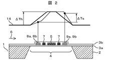
- FIG. 2 is a sectional view taken along line XX ′ in FIG.
- the substrate 2 of the sensor element 1 is made of a material having good thermal conductivity such as silicon or ceramic.
- an electrical insulating film 3 a is formed on the substrate 2, and the cavity is formed by etching the substrate 2 from the back surface to form the diaphragm 4.
- a heating resistor 5 is formed on the surface near the center of the electrical insulating film 3a on the diaphragm 4.
- a heating temperature sensor 7 that detects the heating temperature of the heating resistor 5 is formed around the heating resistor 5 so as to surround the heating resistor 5. The temperature of the heating resistor 5 is detected by the heating temperature sensor 7, and the heating is controlled so as to be higher than the temperature of the air flow 6 by a certain temperature.
- upstream temperature sensors 8 a and 8 b and downstream temperature sensors 9 a and 9 b are formed on both sides of the heating temperature sensor 7. The upstream temperature sensors 8 a and 8 b are arranged upstream of the heating resistor 5, and the downstream temperature sensors 9 a and 9 b are arranged downstream of the heating resistor 5.
- the outermost surface of the sensor element 1 is covered with an electrical insulating film 3b.
- the electrical insulating film 3b serves as a protective film in addition to performing electrical insulation.
- temperature sensitive resistors 10, 11, 12 whose resistance value changes according to the temperature of the air flow 6 are arranged.
- These heating resistors 5, the heating temperature sensor 7, the upstream temperature sensors 8a and 8b, the downstream temperature sensors 9a and 9b, and the temperature sensitive resistors 10, 11, and 12 have a relatively resistance temperature coefficient in which the resistance value varies depending on the temperature.
- Is made of a large material may be formed of a semiconductor material such as polycrystalline silicon or single crystal silicon doped with impurities, or a metal material such as platinum, molybdenum, tungsten, or nickel alloy.
- the electrical insulating films 3a and 3b are formed in a thin film shape with a thickness of about 2 microns from silicon dioxide (SiO 2 ) or silicon nitride (Si 3 N 4 ) so that a sufficient thermal insulation effect can be obtained.
- the heating resistor 5, the heating temperature sensor 7, the upstream temperature sensors 8 a and 8 b, and the downstream temperature sensors 9 a and 9 b are also temperature sensitive resistors in the same manner as the temperature sensitive resistors 10, 11, and 12. is there.
- each resistor constituting the heating resistor 5, the heating temperature sensor 7, the upstream temperature sensors 8a and 8b, the downstream temperature sensors 9a and 9b, and the temperature sensitive resistors 10, 11, and 12 is provided.
- An electrode pad portion 13 on which an electrode for connecting the body to the drive / detection circuit is formed is provided.
- the electrode is made of aluminum or the like.
- the thermal flow meter according to the embodiment of the present invention operates as follows.
- the solid line of the temperature distribution 14 indicates the temperature distribution of the diaphragm 4 when there is no wind.
- the heating resistor 5 is heated so as to be higher than the temperature of the air flow 6 by ⁇ Th.
- the broken line of the temperature distribution 14 is the temperature distribution of the diaphragm 4 when the air flow 6 is generated.
- the upstream side of the heating resistor 5 is cooled by the air flow 6 to lower the temperature, and the downstream side passes through the heating resistor 5 and heated air flows to increase the temperature. Accordingly, the flow rate is measured by measuring the upstream / downstream temperature difference ⁇ Ts between the upstream temperature sensors 8a and 8b and the downstream temperature sensors 9a and 9b.
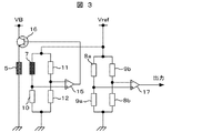
- FIG. 3 shows a drive / detection circuit for the sensor element 1.
- a series circuit composed of the heating temperature sensor 7 and the temperature sensitive resistor 10 whose resistance value varies depending on the temperature of the heating resistor 5 and a series circuit composed of the temperature sensitive resistor 11 and the temperature sensitive resistor 12 are connected in parallel.
- the bridge circuit is configured, and the reference voltage Vref is applied to each series circuit.
- the intermediate voltage of these series circuits is taken out and connected to the amplifier 15.
- the output of amplifier 15 is connected to the 16 bases of the transistors.
- the collector of the transistor 16 is connected to the power supply VB, and the emitter is connected to the heating resistor 5 to constitute a feedback circuit.
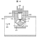
- FIG. 4 shows an embodiment in which the sensor element 1 and the drive / detection circuit are mounted in the intake pipe of an internal combustion engine such as an automobile.
- a base member 19 is provided so as to protrude from the wall surface of the intake pipe line 18.
- the base member 19 is formed with a sub-passage 21 that takes in part of the intake air 20 flowing through the intake pipe 18.
- the sensor element 1 is installed in a rectangular recess formed in the sub passage 21.
- the sub-passage 21 in the part where the sensor element 1 is installed has a linear flow path, and has a curved shape on the upstream and downstream sides.
- the base member 19 is provided with a circuit board 22 on which a drive / detection circuit for the sensor element 1 is mounted, and the sensor element 1 and the circuit board 22 are electrically connected by a gold wire bonding wire 23. Furthermore, a terminal 24 for supplying power to the drive circuit and extracting an output signal is provided, and the circuit board 22 and the terminal 24 are electrically connected by an aluminum bonding wire 25.
- a semiconductor substrate such as single crystal silicon (Si) is used.
- silicon dioxide (SiO 2 ) and silicon nitride (Si 3 N 4 ) to be an electric insulating film 3 a having a predetermined thickness of about 1 ⁇ m are formed by thermal oxidation, CVD, or the like.
- a semiconductor thin film 26 made of polycrystalline silicon (Si) having a thickness of about 1 ⁇ m used as a resistor is laminated by a CVD method or the like. Impurity diffusion is performed on the polycrystalline silicon (Si) semiconductor thin film, and a high concentration doping process is performed so as to obtain a predetermined resistivity.
- the temperature coefficient of resistance of the semiconductor thin film 26 is improved by performing heat treatment in which the sensor element is put into a heating furnace at about 900 ° C. to 1000 ° C. for 1 hour or more, and used as a temperature sensor. Good characteristics were obtained as a resistor.
- the heat treatment conditions are limited to 900 ° C. or less and a few minutes until the MOS transistor characteristics do not change. Therefore, in this step, the semiconductor thin film 26 is kept in a state where impurity diffusion is insufficient and the temperature coefficient of resistance is low.
- the heat treatment condition in which the characteristic variation of the MOS transistor does not occur is not uniformly determined but changes depending on the degree of miniaturization of the semiconductor.
- Step of FIG. 5C After a resist is formed into a predetermined shape by photolithography technology, a polycrystalline silicon (Si) semiconductor thin film is patterned by a method such as reactive ion etching, so that a predetermined heating resistor 5, heating temperature sensor 7, upstream
- a method such as reactive ion etching, so that a predetermined heating resistor 5, heating temperature sensor 7, upstream
- the side temperature sensors 8a and 8b, the downstream temperature sensors 9a and 9b, and the wiring part 30 are obtained.
- Step of FIG. 5D As with electrically insulating film 3a of the electrical insulating film 3b as a protective film is formed by CVD or the like of silicon dioxide (SiO 2) and silicon nitride (Si 3 N 4) of about 1 micron thick.
- an electrode pad portion 13 serving as a terminal for connection to an external circuit is formed of a metal material such as aluminum after removing a part of the electrical insulating film 3b.
- an etching mask material is patterned into a predetermined shape on the back surface of the single crystal silicon (Si) semiconductor substrate 2 and anisotropic etching is performed using an etching solution such as potassium hydroxide (KOH) to form the cavity. Then, the diaphragm 4 is formed.
- KOH potassium hydroxide
- the probe 28 is brought into contact with the electrode pad portion 13, and current is supplied from the power source 27 through the probe 28.
- the wiring portion 30 is electrically connected to the heating resistor 5 (not shown), so that the heating resistor 5 is heated by the current supplied from the power supply 27.
- the current of the power source 27 is adjusted so that the heating temperature sensor 7, the upstream temperature sensors 8a and 8b, and the downstream temperature sensors 9a and 9b are heated at 900 ° C. or more, preferably about 1000 ° C. for 60 minutes or more. To do.
- the specific energization method is shown in FIG.
- the probe 28 is brought into contact with the sensor element 1 formed on the substrate 2 which is a Si wafer.
- One side of the probe 28 is connected to the power source 27, and the other side of the probe 28 is connected to the power source 27 via an ammeter 39.
- the power source 27 is a voltage source, and the heating temperature of the heating resistor 5 can be adjusted by adjusting the voltage V.
- the current source 39 measures the current I flowing through the heating resistor 5. Since the resistance value of the heating resistor 5 varies with temperature, the resistance value (V / I) of the heating resistor 5 is calculated from the voltage V of the power source 27 and the current I of the ammeter 39, thereby generating the heating resistance. The temperature of the body 5 can be measured.
- the heating temperature of the heating resistor 5 can also be calculated from the power consumption (V ⁇ I) of the heating resistor 5. In this case, it is necessary to obtain the relationship between the power and temperature of the heating resistor 5 in advance.
- the heating temperature is calculated from the resistance value of the heating resistor 5, an error is included because the resistance value is changed by the heat treatment.
- the heating temperature can be measured with higher accuracy.
- the heat treatment that was insufficient in the process of FIG. 5B can be performed, and the heating resistor 5, the heating temperature sensor 7, the upstream temperature sensors 8a and 8b, and the downstream temperature sensors 9a and 9b. Impurity diffusion and crystal growth of the resistor can be performed, the resistance temperature coefficient can be improved, and good characteristics as the resistor can be obtained.
- a current when a current is applied to the heating resistor 5 in this step, a current also flows through the wiring 30 to generate heat, but since it is located on the substrate 2, it is dissipated to the substrate 2 and the temperature does not increase.
- the portion having a temperature higher than 900 ° C. can be limited to the portion of the diaphragm 4 that is thermally insulated. Therefore, it is a feature of the present invention that after the diaphragm 4 is formed, the heating resistor 5 is energized and heat-treated.
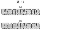
- FIG. 15 is a cross-sectional view showing the crystal state of the heating resistor 5 and the wiring portion 30 after the heat treatment in this step.
- FIG. 15A is a cross section of the wiring portion 30, and FIG. 15B shows a cross section of the heating resistor 5. Since the heating resistor 5 heat-treated in this step is heat-treated at a high temperature, the crystal grows and the crystal grain size increases. On the other hand, since the wiring portion 30 formed of the same material as the heating resistor 5 is not heat-treated in this step, no crystal grows. Therefore, the crystal grain size is different between the part that is heat-treated in this step and the part that is not heat-treated. As the crystal grain size increases, the temperature coefficient of resistance increases, and it is possible to improve the temperature detection sensitivity of the heating resistor and the resistance temperature detector located in the diaphragm 4.
- MOS Metal Oxide Semiconductor
- the sensor element 1 or the sensor element 1 including the semiconductor integrated circuit is completed through the above steps.
- FIG. 6 is an enlarged view of the diaphragm 4 of the sensor element 1.
- the heating temperature sensor 7 on the diaphragm 4 is formed so as to surround the periphery of the heating resistor 5, further extends toward the upstream side of the diaphragm 4, and is connected to the wiring portions 30 e and 30 h. From the heating temperature sensor 7 to the wiring portions 30e and 30h, the semiconductor thin film 26 formed by the process of FIG. 5B is formed by etching.
- the heating temperature sensor 7 and the wiring portions 30e and 30h are originally formed from the same semiconductor thin film 26
- the heating temperature sensor 7 formed on the diaphragm 4 is heat-treated by the process of FIG.
- the heating temperature sensor 7 in the vicinity of the heating resistor 5 and the wiring portions 30e and 30h are different resistances.
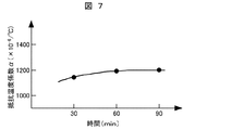
- FIG. 7 shows the relationship between the heat treatment time and the temperature coefficient of resistance when a resistor using a polycrystalline Si thin film is heat treated at 900 ° C. to 1000 ° C.
- FIG. 8 shows the relationship between the heat treatment time and the resistivity when a resistor using a polycrystalline Si thin film is heat treated at 900 ° C. to 1000 ° C. From FIG. 7, the temperature coefficient of resistance of the resistor is improved by applying heat treatment for a long time. 5 (g), the heating temperature sensor 7 positioned on the diaphragm 4 has an improved resistance temperature coefficient, whereas the wiring portions 30e and 30h positioned outside the diaphragm are not heated. The temperature coefficient of resistance does not change.
- the heating temperature sensor 7 has a higher resistance temperature coefficient than the wiring portions 30e and 30h. Therefore, the temperature detection sensitivity is improved by improving the resistance temperature coefficient of the heating temperature sensor 7 by the process of FIG. 5G, and the temperature of the heating resistor 5 can be detected with high accuracy. The temperature of the heating resistor 5 can be accurately controlled. This improves the flow rate detection accuracy.
- the resistivity of the resistor is lowered by applying a large amount of heat treatment.
- the heating temperature sensor 7 positioned on the diaphragm 4 has a low resistivity, whereas the wiring portions 30e and 30h positioned outside the diaphragm are not heated, and thus have resistance. The rate does not change. Therefore, the heating temperature sensor 7 has a lower resistivity than the wiring portions 30e and 30h.
- the heat treatment time is lengthened, the change in resistivity gradually decreases from the result of FIG. 8, and there is a characteristic of saturation at a certain value. If the heat treatment is 90 minutes or longer, the change in resistivity is almost saturated.
- the upstream temperature sensors 8a and 8b on the diaphragm 4 are formed on the upstream side of the heating resistor 5, and further extend toward the upstream side of the diaphragm 4, and are connected to the wiring portions 30a, 30b, 30c, and 30d. .
- These upstream temperature sensors 8a and 8b to the wiring portions 30a, 30b, 30c and 30d are formed by etching the semiconductor thin film 26 formed by the process of FIG. 5B.
- the upstream temperature sensors 8a and 8b and the wiring portions 30a, 30b, 30c, and 30d are originally formed from the same semiconductor thin film 26, but the upstream side formed on the diaphragm 4 by the process of FIG.
- the upstream side temperature sensors 8a and 8b in the vicinity of the heating resistor 5 and the resistors having different characteristics in the wiring portions 30a, 30b, 30c, and 30d are formed. That is, the upstream temperature sensors 8a and 8b have higher resistance temperature coefficients than the wiring portions 30a, 30b, 30c, and 30d. Further, the upstream temperature sensors 8a and 8b have a lower resistivity than the wiring portions 30a, 30b, 30c and 30d. The same applies to the downstream temperature sensors 9a and 9b and the wiring portions 30k, 30l, 30m, and 30n.
- the thermal flow meter can be made smaller and more accurate.
- the diaphragm 4 is obtained by removing all of the substrate 2, but the effect can be obtained even when a part of the substrate 2 is left. That is, if the film thickness of the substrate 2 is different between the part to be heat-treated and the part not to be heat-treated, partial high-temperature heat treatment can be performed, and it can be applied to heat treatment of other semiconductor elements and sensor elements. .
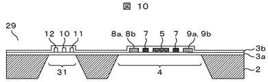
- FIG. 9 is a plan view showing the sensor element 29 in the present embodiment.
- FIG. 10 is a cross-sectional view of the sensor element 1 in FIG.
- the substrate 2 in the portion where the temperature sensitive resistors 10, 11, 12 are formed is removed. That is, in addition to the diaphragm 4, a second diaphragm 31 is provided. The second diaphragm 31 is formed at the same time as the diaphragm 4 in the step of FIG.
- the temperature sensitive resistors 10, 11, and 12 formed on the diaphragm 31 are resistors that form a bridge circuit with the heating temperature sensor 7 in the drive circuit shown in FIG. By this bridge circuit, the heating resistor 5 operates so as to be heated to a predetermined temperature with respect to the air temperature. Therefore, it is desirable that the heating temperature sensor 7 and the temperature sensitive resistors 10, 11, and 12 have substantially the same resistance temperature coefficient. Therefore, it is desirable that the temperature sensitive resistors 10, 11, and 12 be heat-treated in the process of FIG. Accordingly, the diaphragm 4 is provided by removing the substrate 2 where the temperature sensitive resistors 10, 11, 12 are formed, and the temperature sensitive resistors 10, 11, 12 are heated by energization to increase the temperature.
- the resistance temperature coefficient can be improved by heat-treating the resistors 10, 11, and 12.
- the temperature sensitive resistors 10, 11, and 12 can be used as an intake air temperature sensor that detects the temperature of the air.
- the temperature coefficient of resistance is improved by the heat treatment step of FIG. 5G, the detection sensitivity of the air temperature is improved, and high accuracy can be achieved.
- the heat capacity is significantly reduced, and the responsiveness to changes in air temperature can be improved.
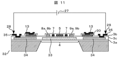
- the configuration of the sensor element 32 of the thermal type flow meter according to this embodiment will be described with reference to FIG. In the present embodiment, the configuration different from that of the first embodiment is described, and the other configurations are the same as those of the first embodiment.
- FIG. 11 is a cross-sectional view showing the sensor element 32 in the present embodiment.
- the heating resistor 33 formed on the diaphragm 4, the heating temperature sensor 7, the upstream temperature sensors 8a and 8b, and the downstream temperature sensors 9a and 9b are provided with the heat treatment heater 33 via the electric insulating film 3c. Is forming.
- the heat treatment heater can be formed in the same process as that of the heating resistor 5, and specifically, the multilayer film is formed by repeating the steps (b), (c), and (d) of FIG. It is possible.
- the electrode of this heat treatment heater is taken out of the diaphragm 4 by the wiring part 34, and the electrode pad part 35 is formed.
- the wiring part 34 is formed of the same film as the heat treatment heater.
- the electrode pad portion 35 is formed in the same manner as the electrode pad portion 13.
- the heat treatment heater 33 is energized and heated, so that the temperature of the diaphragm 4 is increased, and the heating resistor 5, the heating temperature sensor 7, the upstream temperature sensors 8a, 8b, It is characterized in that the downstream temperature sensors 9a and 9b are heat-treated.
- the probe 28 is brought into contact with the electrode pad portion 35 shown in FIG. 11 to adjust the current from the power source 27, and the heating current is supplied to the heat treatment heater 33. is there.
- a region where the heat treatment heater 33 is formed can be widened, and the diaphragm 4 can be heated with a uniform temperature distribution. That is, the heating resistor 5, the heating temperature sensor 7, the upstream temperature sensors 8a and 8b, and the downstream temperature sensors 9a and 9b can be heat-treated at the same temperature.
- the heat treatment is performed by heating the heating resistor 5, the temperature of the resistor located outside in the diaphragm 4 is lowered, and there is a problem that it cannot be heated to an optimum temperature. Accordingly, the temperatures of the upstream temperature sensors 8a and 8b and the downstream temperature sensors 9a and 9b become low, and sufficient heat treatment cannot be performed.
- the temperature in the diaphragm 4 can be made uniform, and the upstream temperature sensors 8a and 8b and the downstream temperature sensors 9a and 9b located in the diaphragm 4 can be heat-treated at an optimum temperature. Become. That is, compared with the first embodiment, the resistance temperature coefficients of the upstream temperature sensors 8a and 8b and the downstream temperature sensors 9a and 9b are improved, and a highly accurate thermal flow meter can be obtained.
- the material of the heat treatment heater 33 can be formed of a polycrystalline Si film as in the first embodiment, but other materials can be selected. For example, it is possible to use metal materials such as platinum, tungsten, tantalum, and molybdenum that are excellent in heat resistance. If a metal material is selected, the thermal conductivity increases and a more uniform temperature distribution can be obtained. Therefore, the heating resistor 5, the heating temperature sensor 7, the upstream temperature sensors 8a and 8b, and the downstream temperature sensors 9a and 9b can be simultaneously heated to the optimum temperature, and the heat treatment can be performed more easily.
- metal materials such as platinum, tungsten, tantalum, and molybdenum that are excellent in heat resistance. If a metal material is selected, the thermal conductivity increases and a more uniform temperature distribution can be obtained. Therefore, the heating resistor 5, the heating temperature sensor 7, the upstream temperature sensors 8a and 8b, and the downstream temperature sensors 9a and 9b can be simultaneously heated to the optimum temperature, and the heat treatment can be performed more easily.
- the diaphragm 4 shown in the first embodiment is provided with a heat treatment heater.
- a heat treatment heater is formed under the temperature sensitive resistors 10, 11, 12 via the electric insulating film 3 c. After removing the substrate 2 where the temperature sensitive resistors 10, 11, 12 are formed and forming the diaphragm 31, the heat sensitive heaters 10, 11, 12 are heat treated by heating the heat treatment heater.
- the heat treatment temperature of the temperature sensitive resistors 10, 11, 12 becomes uniform, and the temperature coefficient of resistance of the temperature sensitive resistors 10, 11, 12 can be made more consistent.
- variation in the resistance balance of the bridge circuit formed by the heating temperature sensor 7 and the temperature sensitive resistors 10, 11 and 12 is reduced, and the temperature control of the heating resistor 5 can be performed with high accuracy.
- FIG. 12 is a cross-sectional view showing the sensor element 36 in the present embodiment.
- a substrate 2 on which the sensor element 36 is formed is integrally provided with a semiconductor integrated circuit 37 that drives the sensor element and detects the flow rate.
- the transistor 16, the amplifier 15, the amplifier 17, and the like shown in FIG. 3 are included in the semiconductor integrated circuit 37.
- a heat treatment is performed by supplying current to the electrode pad portion 13 from the power source 27 via the probe 28 and heating it.
- a current is supplied to the heating resistor 5 through the semiconductor integrated circuit 37.
- the semiconductor integrated circuit 37 By providing an arithmetic unit, a switch, or the like in the semiconductor integrated circuit 37, the current supplied to the heating resistor 5 can be controlled. Therefore, unlike the first embodiment, there is no need to provide the electrode pad portion 13 for contacting the probe 28. Since it is not necessary to provide the electrode pad portion 13 for heat treatment, the area of the sensor element 36 can be reduced.
- FIG. 14 shows an example in which the sensor element 36 is mounted by the molding material 40.
- the sensor element 36 is disposed on the lead frame 41 and connects the electrode pad 45 formed on the sensor element 36 and the lead frame 43 with a bonding wire.
- the electrode pad 45 is provided with a power supply terminal for driving the sensor element 36, an output terminal for extracting the detected flow rate signal, a communication terminal for performing digital communication with the semiconductor integrated circuit 37, and the like.
- the lead frame 43 is connected to a power source of the thermal flow meter and a connector for taking out a signal to the outside.
- the mold material 40 an epoxy resin is used and manufactured by known injection molding.
- the molding material 40 is formed so as to avoid the diaphragm 4 so that the diaphragm 4 of the sensor element 36 is exposed to air.
- a through hole 42 is formed in the lead frame 41 and the mold material 40 on the back surface side of the sensor element 36 so that the back surface side of the diaphragm 4 is not sealed.
- Injection molding has a small variation in the shape of the molding material and can be manufactured at a low cost, so that the variation in mounting of sensor elements can be reduced. Since the manufacturing variation is small, the sensor element can be miniaturized.
- the resistors such as the heating resistor 5, the heating temperature sensor 7, the upstream temperature sensors 8a and 8b, and the downstream temperature sensors 9a and 9b are formed of polycrystalline Si. But it can also be formed.
- a semiconductor material such as single crystal silicon or polycrystalline silicon into which impurities are introduced, or a metal material such as platinum, tungsten, tantalum, or molybdenum can be used.
- the metal material has a temperature coefficient of resistance of 2000 ppm / ° C. or higher, and a highly sensitive sensor element can be obtained. Since platinum, which is a metal material, starts crystal growth at 800 ° C. or higher, heat treatment at 800 ° C. or higher is necessary. Preferably, a resistor having good characteristics can be obtained by heat treatment at 900 ° C. Further, since molybdenum begins crystal growth at 700 ° C. or higher, heat treatment at 700 ° C. or higher is required, and a resistor having a high resistance temperature coefficient can be obtained by heat treatment at 1000 ° C. preferably.
- the heat treatment temperature in the step shown in FIG. Specifically, the effect can be obtained by performing heat treatment at a temperature of 800 ° C. or higher in the case of platinum and 700 ° C. or higher in the case of molybdenum.
- a heat treatment is performed by heating to 900 ° C. for platinum and 1000 ° C. for molybdenum to obtain a resistor having a high temperature coefficient of resistance and reduced influence of variations in heat treatment time, and a polycrystalline Si thin film is used.
- the thermal flow meter is more sensitive than if it were.
Landscapes
- Physics & Mathematics (AREA)
- Fluid Mechanics (AREA)
- General Physics & Mathematics (AREA)
- Measuring Volume Flow (AREA)
Abstract
Description
基板2としては、単結晶ケイ素(Si)等の半導体基板を用いる。ベースとなる基板2の表面を、熱酸化やCVD法等により所定の厚さ約1μmの電気絶縁膜3aとなる二酸化ケイ素(SiO2)と窒化ケイ素(Si3N4)を形成する。
次に、抵抗体として用いる厚さ約1μmの多結晶ケイ素(Si)からなる半導体薄膜26をCVD法等により積層する。多結晶ケイ素(Si)半導体薄膜に不純物拡散を行い、所定の抵抗率となるように高濃度ドープ処理を行う。従来、この不純物の導入・拡散工程で、センサ素子を900℃~1000℃程度の加熱炉に1時間以上投入する熱処理を行うことにより、半導体薄膜26の抵抗温度係数を向上させ、温度センサとして用いる抵抗体として良好な特性を得ていた。しかし、基板2上に半導体集積回路としてMOS(Metal Oxide Semiconductor)トランジスタを予め形成している場合(図示なし)、900℃~1000℃の熱処理を行ってしまうと、MOSトランジスタの特性変動(例えば、ソース、ドレイン領域の拡大)により、半導体集積回路に動作不良が発生してしまう。そのため、例えばゲート長が1μm程度のCMOSプロセスでは、900℃以下、数分程度まででMOSトランジスタの特性変動が起きない熱処理条件に制限しておく。したがって、本工程では半導体薄膜26は、不純物拡散が不十分であり、抵抗温度係数も低い状態にとどめておく。ここで、MOSトランジスタの特性変動が起きない熱処理条件とは、一律に決まるものではなく、半導体の微細化の程度等によって変化するものである。
ホトリソグラフィ技術によりレジストを所定の形状に形成した後、反応性イオンエッチング等の方法により、多結晶ケイ素(Si)半導体薄膜をパターニングすることで、所定の発熱抵抗体5,加熱温度センサ7,上流側温度センサ8a,8b,下流側温度センサ9a,9b,配線部30が得られる。
その後工程では、保護膜として電気絶縁膜3bを電気絶縁膜3aと同様に、二酸化ケイ素(SiO2)と窒化ケイ素(Si3N4)を約1ミクロン厚にCVD法等により形成する。
次に、外部回路との接続のための端子となる電極パッド部13が、電気絶縁膜3bの一部を除去した後、アルミニウム等の金属材料で形成される。
次に、単結晶ケイ素(Si)半導体基板2の裏面にエッチングのマスク材を所定の形状にパターニングし、水酸化カリウム(KOH)等のエッチング液を用いて異方性エッチングすることにより空洞部を形成して、ダイアフラム4を形成する。
次に、電極パッド部13にプローブ28を接触させ、プローブ28を通して電源27から電流を供給する。配線部30は、発熱抵抗体5に電気的に接続しておく(図示なし)ことにより、電源27から供給した電流により発熱抵抗体5が加熱される。このとき、加熱温度センサ7,上流側温度センサ8a,8b,下流側温度センサ9a,9bが900℃以上、好ましくは1000℃程度で、60分以上加熱されるように、電源27の電流を調整する。
2 基板
3a,3b,3c 電気絶縁膜
4,31 ダイアフラム
5 発熱抵抗体
6 空気流
7 加熱温度センサ
8a,8b 上流側温度センサ
9a,9b 下流側温度センサ
10,11,12 感温抵抗体
13,35 電極パッド部
14 温度分布
15,17 増幅器
16 トランジスタ
18 吸気管路
19 ベース部材
20 吸気
21 副通路
22 回路基板
23 金線ボンディングワイヤー
24 端子
25 アルミボンディングワイヤー
26 半導体薄膜
27 電源
28 プローブ
30,30a~n,34,38 配線部
33 熱処理用ヒータ
37 半導体集積回路
39 電流計
40 モールド材
41,43 リードフレーム
42 貫通孔
44 ボンディングワイヤー
45 電極パッド
Claims (11)
- 半導体基板に形成された空洞部と、
前記空洞部を覆うように設けられた絶縁膜により形成された薄膜部と、
前記絶縁膜の間に形成された、発熱抵抗体および測温抵抗体と、を有する熱式流量計の製造方法において、
前記薄膜部を形成した後に前記薄膜部を加熱し、前記発熱抵抗体及び前記測温抵抗体の結晶粒径を成長させる熱処理を行うことを特徴とする熱式流量計の製造方法。 - 請求項1記載の熱式流量計の製造方法において、
前記熱処理は、前記発熱抵抗体を通電することにより前記発熱抵抗体を高温に加熱し、前記発熱抵抗体及び前記測温抵抗体の結晶粒径を成長させる熱処理であることを特徴とする熱式流量計の製造方法。 - 請求項1記載の熱式流量計の製造方法において、
前記薄膜部には第2の発熱抵抗体が設けられており、
前記熱処理は、前記第2の発熱抵抗体を通電することにより前記第2の発熱抵抗体を加熱し、前記発熱抵抗体及び測温抵抗体の結晶粒径を成長させる熱処理であることを特徴とする熱式流量計の製造方法。 - 請求項1記載の熱式流量計の製造方法において、
前記半導体基板上に第2の薄膜部を形成する工程を有し、
前記第2の薄膜部には第2の測温抵抗体が形成されており、
前記第2の薄膜部を形成した後に、前記第2の薄膜部を加熱し、前記第2の測温抵抗体の結晶粒径を成長させる熱処理を行うことを特徴とした熱式流量計。 - 請求項4記載の熱式流量計の製造方法において、
前記第2の薄膜部には第2の発熱抵抗体が設けられており、前記第2の発熱抵抗体を通電することにより前記第2の薄膜部を加熱し、前記第2の発熱抵抗体の結晶粒径を成長させる熱処理を行うことを特徴とした熱式流量計。 - 半導体基板に形成された空洞部と、前記空洞部を覆うように設けられた絶縁膜により形成された薄膜部と、前記絶縁膜の間に形成された、発熱抵抗体および測温抵抗体と、を有する熱式流量計において、
前記発熱抵抗体に接続され前記薄膜部の外側に延設される引き出し配線部を備え、
前記引き出し配線部の前記薄膜部の外側に位置する部分の抵抗温度係数は、前記発熱抵抗体の抵抗温度係数よりも小さく、かつ、
前記引き出し配線部の前記薄膜部の外側に位置する部分の抵抗率は、前記発熱抵抗体の抵抗率よりも大きいことを特徴とする熱式流量計。 - 請求項6記載の熱式流量計において、
前記薄膜部に第2の発熱抵抗体を設け、前記第2の発熱抵抗体を通電するための通電パッドが設けられていることを特徴とする熱式流量計。 - 請求項6記載の熱式流量計において、
前記半導体基板上に第2の薄膜部が形成されており、
前記第2の薄膜部は、第2の測温抵抗体が形成されており、
前記第2の測温抵抗体に接続され前記第2の薄膜部の外側に延設される第2の引き出し配線部を備え、
前記第2の引き出し配線部の前記第2の薄膜部の外側に位置する部分の抵抗温度係数は、前記第2の測温抵抗体の抵抗温度係数よりも小さく、かつ、
前記第2の引き出し配線部の前記第2の薄膜部の外側に位置する部分の抵抗率は、前記第2の測温抵抗体の抵抗率よりも大きいことを特徴とする熱式流量計。 - 請求項8記載の熱式流量計において、
前記第2の薄膜部は、第2の発熱抵抗体が形成されており、
前記第2の発熱抵抗体に接続され前記第2の薄膜部の外側に延設される第3の引き出し配線部を備え、
前記第3の引き出し配線部の前記第2の薄膜部の外側に位置する部分の抵抗温度係数は、前記第2の発熱抵抗体の抵抗温度係数よりも小さく、かつ、
前記第3の引き出し配線部の前記第2の薄膜部の外側に位置する部分の抵抗率は、前記第2の発熱抵抗体の抵抗率よりも大きいことを特徴とする熱式流量計。 - 請求項6乃至9記載のいずれかの熱式流量計において、
前記半導体基板上に駆動・検出・信号処理を行う半導体トランジスタからなる集積回路を設けたことを特徴とする熱式流量計。 - 請求項10記載の熱式流量計において、
前記半導体基板は、リードフレーム上に配置され、
前記半導体基板および前記リードフレームをモールド材でモールドしたことを特徴とする熱式流量計。
Priority Applications (5)
| Application Number | Priority Date | Filing Date | Title |
|---|---|---|---|
| PCT/JP2011/001197 WO2012117446A1 (ja) | 2011-03-02 | 2011-03-02 | 熱式流量計 |
| US13/984,748 US20130313675A1 (en) | 2011-03-02 | 2011-03-02 | Thermal Type Flowmeter |
| EP11859960.4A EP2682720B1 (en) | 2011-03-02 | 2011-03-02 | Heat-type flow meter |
| CN201180067266.2A CN103380353B (zh) | 2011-03-02 | 2011-03-02 | 热式流量计 |
| JP2013502043A JP5857032B2 (ja) | 2011-03-02 | 2011-03-02 | 熱式流量計 |
Applications Claiming Priority (1)
| Application Number | Priority Date | Filing Date | Title |
|---|---|---|---|
| PCT/JP2011/001197 WO2012117446A1 (ja) | 2011-03-02 | 2011-03-02 | 熱式流量計 |
Publications (1)
| Publication Number | Publication Date |
|---|---|
| WO2012117446A1 true WO2012117446A1 (ja) | 2012-09-07 |
Family
ID=46757422
Family Applications (1)
| Application Number | Title | Priority Date | Filing Date |
|---|---|---|---|
| PCT/JP2011/001197 Ceased WO2012117446A1 (ja) | 2011-03-02 | 2011-03-02 | 熱式流量計 |
Country Status (5)
| Country | Link |
|---|---|
| US (1) | US20130313675A1 (ja) |
| EP (1) | EP2682720B1 (ja) |
| JP (1) | JP5857032B2 (ja) |
| CN (1) | CN103380353B (ja) |
| WO (1) | WO2012117446A1 (ja) |
Families Citing this family (14)
| Publication number | Priority date | Publication date | Assignee | Title |
|---|---|---|---|---|
| US9820379B2 (en) * | 2011-06-08 | 2017-11-14 | Kyocera Corporation | Circuit board and electronic device including same |
| CN104034378B (zh) * | 2014-06-27 | 2017-02-15 | 天津大学 | 恒流法热式气体质量流量计及其测量方法 |
| JP6438706B2 (ja) * | 2014-08-22 | 2018-12-19 | 日立オートモティブシステムズ株式会社 | センサ装置 |
| CN104406644B (zh) * | 2014-12-05 | 2018-04-10 | 北京时代民芯科技有限公司 | 一种mems热式流量传感器及其制造方法 |
| US9567209B1 (en) * | 2015-09-03 | 2017-02-14 | Taiwan Semiconductor Manufacturing Company Ltd. | Semiconductor structure and manufacturing method thereof |
| US10347814B2 (en) * | 2016-04-01 | 2019-07-09 | Infineon Technologies Ag | MEMS heater or emitter structure for fast heating and cooling cycles |
| US10955599B2 (en) | 2016-04-01 | 2021-03-23 | Infineon Technologies Ag | Light emitter devices, photoacoustic gas sensors and methods for forming light emitter devices |
| US10681777B2 (en) | 2016-04-01 | 2020-06-09 | Infineon Technologies Ag | Light emitter devices, optical filter structures and methods for forming light emitter devices and optical filter structures |
| CN105865552A (zh) * | 2016-04-08 | 2016-08-17 | 东南大学 | 一种基于mems工艺的集成阵列式薄膜气体流量传感器及其加工方法 |
| CN109991043B (zh) * | 2017-12-31 | 2022-07-05 | 中国人民解放军63653部队 | 基于高温管式气氛炉的差压式取气测量系统 |
| CN108158039B (zh) * | 2018-01-03 | 2023-07-11 | 云南中烟工业有限责任公司 | 一种集成多个Pt温度传感器的MEMS发热芯片及其制造方法 |
| CN108354228B (zh) * | 2018-01-03 | 2023-07-25 | 云南中烟工业有限责任公司 | 一种集成Pt温度传感器的MEMS发热芯片及其制造方法 |
| US20200243413A1 (en) * | 2019-01-30 | 2020-07-30 | Avago Technologies International Sales Pte. Limited | Methods, devices, and systems for substrate temperature measurements |
| JP2021012134A (ja) * | 2019-07-08 | 2021-02-04 | 株式会社デンソー | 熱式流量センサ |
Citations (7)
| Publication number | Priority date | Publication date | Assignee | Title |
|---|---|---|---|---|
| JPS61170618A (ja) * | 1985-01-24 | 1986-08-01 | Toyota Central Res & Dev Lab Inc | 流速検出用半導体センサ |
| JPH02120624A (ja) * | 1988-10-29 | 1990-05-08 | Ngk Insulators Ltd | 検知素子の製造法 |
| WO2001084088A1 (en) * | 2000-05-02 | 2001-11-08 | Hitachi, Ltd. | Device for measuring physical quantity, method of manufacture thereof, and vehicle control system using device for measuring physical quantity |
| JP2002286521A (ja) * | 2001-03-26 | 2002-10-03 | Denso Corp | 流量測定装置の製造方法 |
| JP2003075222A (ja) * | 2001-09-04 | 2003-03-12 | Hitachi Ltd | ガス流量計及びその製造方法 |
| JP2005321294A (ja) * | 2004-05-10 | 2005-11-17 | Mitsubishi Electric Corp | 感熱式流量検出素子の製造方法 |
| JP2010160092A (ja) * | 2009-01-09 | 2010-07-22 | Denso Corp | 流量センサ |
Family Cites Families (4)
| Publication number | Priority date | Publication date | Assignee | Title |
|---|---|---|---|---|
| JP3698679B2 (ja) * | 2002-03-27 | 2005-09-21 | 株式会社日立製作所 | ガス流量計及びその製造方法 |
| US6983653B2 (en) * | 2002-12-13 | 2006-01-10 | Denso Corporation | Flow sensor having thin film portion and method for manufacturing the same |
| JP4882732B2 (ja) * | 2006-12-22 | 2012-02-22 | 株式会社デンソー | 半導体装置 |
| JP2008170382A (ja) * | 2007-01-15 | 2008-07-24 | Hitachi Ltd | 熱式流体流量センサ及びその製造方法 |
-
2011
- 2011-03-02 US US13/984,748 patent/US20130313675A1/en not_active Abandoned
- 2011-03-02 WO PCT/JP2011/001197 patent/WO2012117446A1/ja not_active Ceased
- 2011-03-02 JP JP2013502043A patent/JP5857032B2/ja not_active Expired - Fee Related
- 2011-03-02 EP EP11859960.4A patent/EP2682720B1/en active Active
- 2011-03-02 CN CN201180067266.2A patent/CN103380353B/zh not_active Expired - Fee Related
Patent Citations (7)
| Publication number | Priority date | Publication date | Assignee | Title |
|---|---|---|---|---|
| JPS61170618A (ja) * | 1985-01-24 | 1986-08-01 | Toyota Central Res & Dev Lab Inc | 流速検出用半導体センサ |
| JPH02120624A (ja) * | 1988-10-29 | 1990-05-08 | Ngk Insulators Ltd | 検知素子の製造法 |
| WO2001084088A1 (en) * | 2000-05-02 | 2001-11-08 | Hitachi, Ltd. | Device for measuring physical quantity, method of manufacture thereof, and vehicle control system using device for measuring physical quantity |
| JP2002286521A (ja) * | 2001-03-26 | 2002-10-03 | Denso Corp | 流量測定装置の製造方法 |
| JP2003075222A (ja) * | 2001-09-04 | 2003-03-12 | Hitachi Ltd | ガス流量計及びその製造方法 |
| JP2005321294A (ja) * | 2004-05-10 | 2005-11-17 | Mitsubishi Electric Corp | 感熱式流量検出素子の製造方法 |
| JP2010160092A (ja) * | 2009-01-09 | 2010-07-22 | Denso Corp | 流量センサ |
Also Published As
| Publication number | Publication date |
|---|---|
| EP2682720B1 (en) | 2019-09-18 |
| EP2682720A1 (en) | 2014-01-08 |
| CN103380353B (zh) | 2015-08-05 |
| JP5857032B2 (ja) | 2016-02-10 |
| US20130313675A1 (en) | 2013-11-28 |
| JPWO2012117446A1 (ja) | 2014-07-07 |
| CN103380353A (zh) | 2013-10-30 |
| EP2682720A4 (en) | 2014-08-27 |
Similar Documents
| Publication | Publication Date | Title |
|---|---|---|
| JP5857032B2 (ja) | 熱式流量計 | |
| CN101308036B (zh) | 热式流量计 | |
| JP4839395B2 (ja) | 熱式流量計 | |
| JP5315304B2 (ja) | 熱式流量計 | |
| CN103052866B (zh) | 热式流量传感器 | |
| US6557411B1 (en) | Heating element type mass air flow sensor, and internal combustion engine-control apparatus using the sensor | |
| US8689608B2 (en) | Thermal gas sensor | |
| CN102735298B (zh) | 热式流体流量传感器 | |
| EP2060880B1 (en) | Thermal type flow sensor | |
| JP3698679B2 (ja) | ガス流量計及びその製造方法 | |
| US4733559A (en) | Thermal fluid flow sensing method and apparatus for sensing flow over a wide range of flow rates | |
| US4633578A (en) | Miniature thermal fluid flow sensors and batch methods of making same | |
| CN102052942A (zh) | 热式流体流量传感器及其制造方法 | |
| JP4558647B2 (ja) | 熱式流体流量計 | |
| CN101498596A (zh) | 热式流体流量传感器 | |
| JP3468731B2 (ja) | 熱式空気流量センサ、素子および内燃機関制御装置 | |
| JP2004257870A (ja) | 流量センサ | |
| JP5492834B2 (ja) | 熱式流量計 | |
| JPH11258021A (ja) | 熱式空気流量センサ | |
| JP6532810B2 (ja) | 流量センサ | |
| JPS63293419A (ja) | フロ−センサ |
Legal Events
| Date | Code | Title | Description |
|---|---|---|---|
| 121 | Ep: the epo has been informed by wipo that ep was designated in this application |
Ref document number: 11859960 Country of ref document: EP Kind code of ref document: A1 |
|
| WWE | Wipo information: entry into national phase |
Ref document number: 2011859960 Country of ref document: EP |
|
| WWE | Wipo information: entry into national phase |
Ref document number: 13984748 Country of ref document: US |
|
| ENP | Entry into the national phase |
Ref document number: 2013502043 Country of ref document: JP Kind code of ref document: A |
|
| NENP | Non-entry into the national phase |
Ref country code: DE |