WO2012127744A1 - 光学部材及びその製造方法 - Google Patents
光学部材及びその製造方法 Download PDFInfo
- Publication number
- WO2012127744A1 WO2012127744A1 PCT/JP2011/079017 JP2011079017W WO2012127744A1 WO 2012127744 A1 WO2012127744 A1 WO 2012127744A1 JP 2011079017 W JP2011079017 W JP 2011079017W WO 2012127744 A1 WO2012127744 A1 WO 2012127744A1
- Authority
- WO
- WIPO (PCT)
- Prior art keywords
- optical member
- aluminum
- dielectric layer
- degrees
- layer
- Prior art date
- Legal status (The legal status is an assumption and is not a legal conclusion. Google has not performed a legal analysis and makes no representation as to the accuracy of the status listed.)
- Ceased
Links
Images



Classifications
-
- G—PHYSICS
- G02—OPTICS
- G02B—OPTICAL ELEMENTS, SYSTEMS OR APPARATUS
- G02B1/00—Optical elements characterised by the material of which they are made; Optical coatings for optical elements
- G02B1/10—Optical coatings produced by application to, or surface treatment of, optical elements
- G02B1/11—Anti-reflection coatings
- G02B1/118—Anti-reflection coatings having sub-optical wavelength surface structures designed to provide an enhanced transmittance, e.g. moth-eye structures
-
- B—PERFORMING OPERATIONS; TRANSPORTING
- B29—WORKING OF PLASTICS; WORKING OF SUBSTANCES IN A PLASTIC STATE IN GENERAL
- B29D—PRODUCING PARTICULAR ARTICLES FROM PLASTICS OR FROM SUBSTANCES IN A PLASTIC STATE
- B29D11/00—Producing optical elements, e.g. lenses or prisms
- B29D11/00009—Production of simple or compound lenses
-
- G—PHYSICS
- G02—OPTICS
- G02B—OPTICAL ELEMENTS, SYSTEMS OR APPARATUS
- G02B1/00—Optical elements characterised by the material of which they are made; Optical coatings for optical elements
- G02B1/10—Optical coatings produced by application to, or surface treatment of, optical elements
- G02B1/11—Anti-reflection coatings
-
- G—PHYSICS
- G02—OPTICS
- G02B—OPTICAL ELEMENTS, SYSTEMS OR APPARATUS
- G02B1/00—Optical elements characterised by the material of which they are made; Optical coatings for optical elements
- G02B1/10—Optical coatings produced by application to, or surface treatment of, optical elements
- G02B1/12—Optical coatings produced by application to, or surface treatment of, optical elements by surface treatment, e.g. by irradiation
Definitions
- the present invention relates to an optical member and a method for manufacturing the optical member.
- an optical member comprising a base material and an antireflection film supported by a thin film layer provided on the base material and having fine irregularities provided on the thin film layer, the fine member The projections and depressions are formed by plate crystals mainly composed of alumina, and the thin film layer is proposed as an optical member made of an oxide containing at least one selected from zirconia, silica, titania, and zinc oxide.
- the method for forming fine irregularities is liquid phase film formation (sol-gel method)
- the affinity with the oxide thin film stacking method conventionally used for lenses is low.
- the process of forming a thin film on a base material is increasing. Furthermore, there was a problem that the coating property to a structure in which liquids such as film adhesion and concave surface were liable to accumulate was poor.
- Patent Document 2 describes that aluminum metal is vacuum-deposited on a base material and hydrothermally treated to form a fine concavo-convex structure on the surface. However, Patent Document 2 does not describe a lens having a curvature as a base material, and does not describe forming a dielectric layer between the base material and the fine concavo-convex structure.
- the optical member capable of preventing the reflection of the entire surface of the substrate having a curved surface at least partially or the reflection of a specific portion of the substrate, and the control of the film thickness are easy, the film adhesion is high, and the curved surface is at least partially. It is possible to easily form even a structure that does not easily cause a liquid phase reaction, such as a substrate having a dielectric layer, and deposits at least one of aluminum and alumina without breaking the vacuum after forming the dielectric layer by vapor phase film formation It is desired to provide a method for manufacturing an optical member that can be used.
- the present invention provides an optical member that can prevent reflection of the entire surface of a substrate having a curved surface at least in part or antireflection of a specific portion of the substrate, and can easily control the film thickness. It is possible to easily form even a structure that is difficult to cause a liquid phase reaction such as a substrate having a curved surface, and after forming a dielectric layer by vapor phase film deposition, at least one of aluminum and alumina is deposited without breaking the vacuum
- An object of the present invention is to provide a method for manufacturing an optical member that can be used.
- the optical member of the present invention comprises a base material having a curved surface at least in part, and a layer in which at least one of aluminum alone and a compound containing aluminum is vapor-phase-deposited on the base material by hydrothermal treatment Has an uneven structure, A dielectric layer formed by vapor deposition is provided between the base material and the concavo-convex structure.
- the conventional problems can be solved, the optical member capable of preventing the reflection of the entire surface of the substrate having a curved surface at least in part or the reflection of a specific part of the substrate, and the control of the film thickness are easy. It can be easily formed even with a structure that has high film adhesion and is difficult to cause a liquid phase reaction such as a substrate having a curved surface at least in part, and without breaking the vacuum after forming the dielectric layer by vapor deposition
- the manufacturing method of the optical member which can vapor-deposit at least any one of aluminum and an alumina can be provided.
- FIG. 1 is a schematic diagram showing a concave meniscus lens used in Example 1.
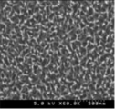
- FIG. FIG. 2 is a photograph showing the results of observation of the optical member of Example 1 by FE-SEM.
- FIG. 3 is a photograph showing a cross-sectional SEM of the optical member of Example 1.
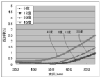
- FIG. 4 is a graph showing the reflectance at the incident angles of 5 degrees, 12 degrees, 30 degrees, and 45 degrees in the optical member of Example 1.
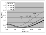
- FIG. 5 is a graph showing the reflectance at the incident angles of 5 degrees, 12 degrees, 30 degrees, and 45 degrees in the optical member of Example 2.
- FIG. 6 is a graph showing the reflectance at the incident angles of 5 degrees, 12 degrees, 30 degrees, and 45 degrees in the optical member of Example 12.
- the optical member of the present invention comprises a base material having a curved surface at least in part, and a layer in which at least one of aluminum alone and a compound containing aluminum is vapor-phase-deposited on the base material by hydrothermal treatment Has a concavo-convex structure, a dielectric layer, and, if necessary, other members.
- the substrate include a transparent glass substrate, a resin molded body, a synthetic resin sheet, a synthetic resin film, a ceramic plate, and a metal plate.
- a transparent glass substrate, a synthetic resin sheet, and a synthetic resin film are particularly preferable.
- the material of the transparent glass substrate include white plate glass, blue plate glass, green glass, and silica-coated blue plate glass.
- high refractive index glass or light diffusion glass in which fine particles are dispersed inside the glass can also be used.
- the material of the resin molded body, the synthetic resin sheet, and the synthetic resin film include polyethylene terephthalate (PET), polycarbonate, polyethersulfone, polyester, acrylic resin, vinyl chloride resin, aromatic polyamide resin, and polyamideimide. , Polyimide, FRP (fiber reinforced plastic), TAC (triacetyl cellulose), cycloolefin polymer (manufactured by ZEON Corporation, trade name ZEONOR, trade name ZEONEX), and the like.
- the curved surface may be at least part of the base material, and may have a two-dimensional or three-dimensional curved surface as a whole.
- a lens having a curvature is suitable.
- the lens include a concave meniscus lens, a concave lens, a convex lens, an aspherical lens, and a cylindrical lens.
- the substrate having a curved surface at least in part includes a structure having a large curvature, and an optical member that also receives high-angle incident light such as an optical member (for example, a prism) disposed obliquely with respect to incident light.
- an optical member for example, a prism
- the compound containing aluminum include aluminum oxide and a compound in which oxygen vacancies are generated in the aluminum oxide.
- the method for vapor-phase film-forming at least one of the aluminum simple substance and the compound containing aluminum is not particularly limited and can be appropriately selected from known ones according to the purpose. There are two types: chemical vapor deposition and physical vapor deposition. Examples of the chemical vapor deposition include plasma CVD, laser CVD, thermal CVD, and gas source CVD. Examples of the physical vapor deposition include sputtering, electron beam vapor deposition, resistance heating vapor deposition, and molecular beam epitaxy. Among these, the electron beam evaporation method is particularly preferable.
- atmospheric pressure vapor deposition for example, deposition by atmospheric CVD is also possible.
- the compatibility with the vapor phase film formation method of the dielectric layer conventionally used for antireflection of the lens is high, and the complex base such as film thickness controllability, film adhesion, concave surface, etc. There is a merit that the material can be easily formed.
- the average thickness of the outermost layer made of aluminum formed by vapor deposition is preferably 100 nm or less, more preferably 1 nm to 80 nm.
- a boehmite layer that remains as a dense layer without forming a fine uneven structure is generated under the fine uneven structure (about 200 nm or more).
- This boehmite layer causes optical interference strongly and adversely affects the broadband antireflection of the entire visible light.
- the average thickness of the outermost layer made of aluminum exceeds 100 nm, the time required for hydrothermal treatment becomes large (about 10 minutes or more when boiling water is used), and the processing takes time. There is a possibility that the influence of hydrothermal treatment on the material is increased.
- the average thickness of the outermost layer made of alumina formed by vapor deposition is preferably 150 nm or less, more preferably 2 nm to 120 nm.
- a boehmite layer that remains as a dense layer without forming a fine concavo-convex structure is generated under the fine concavo-convex structure as in the case of aluminum (thickness of about 200 nm or more).
- the boehmite layer causes strong optical interference and adversely affects the broadband antireflection of the entire visible light.
- the average thickness of the outermost layer made of alumina exceeds 150 nm, the time required for hydrothermal treatment becomes large (about 10 minutes or more when boiling water is used), and the processing takes time. There is a possibility that the influence of hydrothermal treatment is increased on the material.
- the concavo-convex structure is formed on the base material by hydrothermally treating the outermost layer on which at least one of aluminum and alumina is vapor-phase formed. As described above, the outermost layer is composed of an uneven structure and a dense layer.
- hydrothermal treatment There is no restriction
- the outermost layer formed by vapor-phase deposition of at least one of aluminum and alumina formed on the base material is subjected to peptization and the like, and the outermost layer of both aluminum and alumina is boehmite (hydrated) Converted to aluminum oxide, Al 2 O 3 (H 2 O)).
- the boehmite layer has a very slight action of dissolving in water or an aqueous solution, and when it is dissolved, a force that pulls the boehmite layer works (cavitation effect). Since this force is generated evenly to some extent on the whole, a fine concavo-convex structure is formed on the whole with an average pitch of about 100 nm.
- the temperature of the hot water is preferably 80 ° C. to 100 ° C.
- the immersion time of hot water varies depending on the thickness of the formed aluminum and alumina layers, but is about 1 second to 30 minutes, and most preferably about 10 seconds to 10 minutes.
- the height of the convex portion in the fine concavo-convex structure may be reduced due to elution.
- it is preferable to continue to soak in boiling water because it may adversely affect other base materials and dielectric layers.
- Examples of the alkali in the alkaline aqueous solution of (2) above 60 ° C. and below the boiling temperature include amine-based solutions such as sodium hydroxide, potassium hydroxide and triethanolamine, and ammonia. Among these, it is preferable to use an amine-based solution, and triethanolamine is particularly preferable because it has an effect of preventing the precipitation of eluted aluminum on the glass substrate due to a chelate reaction.
- the temperature of the alkaline aqueous solution is preferably 60 ° C. to 100 ° C.
- the immersion time of the alkaline aqueous solution is about 1 second to 30 minutes, and most preferably about 10 seconds to 10 minutes.
- the hydrothermal treatment (3) is preferably a treatment exposed to water vapor. The treatment time of the exposure to water vapor is about 1 minute to 24 hours.
- the average height of the protrusions in the uneven structure is preferably 5 nm to 1,000 nm, and more preferably 20 nm to 500 nm. If the average height of the protrusions is less than 5 nm, the phenomenon that the refractive index gradually changes due to fine unevenness may be almost ineffective because it is too thin for visible light. If it exceeds, the aspect ratio with respect to the pitch becomes too large, so that it may become weak against mechanical strength and dirt.
- the average height of the protrusions in the concavo-convex structure can be measured by, for example, an SEM observation image of a cross-sectional structure.
- the thickness of the concavo-convex structure (height of the convex portion) is calculated by measuring the distance between the tip and bottom of the metal sputtered portion, and the dense layer thickness is calculated by measuring the distance from the bottom to the glass interface. did.
- FIG. 3 is a SEM cross-sectional image of a sample (optical member) produced by this method.
- As another method for calculating the thickness of the concavo-convex structure there is a method of observing the surface with AFM. At this time, since the pitch of the surface is very small, it is necessary to pay attention to an error caused by the thickness of the AFM needle especially at the bottom.
- the dielectric layer is a film formed by vapor deposition between the base material and the concavo-convex structure.
- the dielectric layer is formed on the base material by vapor deposition, and the refractive index and material are not particularly limited.
- the refractive index and material are not particularly limited.
- the antireflection effect can be further improved, or a dielectric layer having a property such as SiO 2 that hardly allows water to pass through can be formed. It can be used to exert effects such as mitigating the influence on the material.
- a method for forming the dielectric layer is not particularly limited and may be appropriately selected depending on the intended purpose.
- Examples thereof include a vacuum evaporation method (electron beam evaporation method, resistance heating evaporation method), a sputtering method, and an ion plate.
- Chemical vapor deposition (CVD) methods such as physical vapor deposition (PVD) methods such as ting method, ion beam method, ion assist method, laser ablation method, thermal CVD method, photo CVD method, plasma CVD method, etc. Can be mentioned.
- the physical vapor deposition (PVD) method is preferable, and the sputtering method and the vacuum evaporation method are particularly preferable as methods that have been conventionally used for the dielectric layer antireflection structure.
- the dielectric layer is a dielectric multilayer film composed of two or more dielectric layers, since there are more reflective surfaces than a single-layer film, it is easy to control optical interference, and various optical characteristics ( It is easy to apply as an anti-reflective application to a base material having a refractive index, etc., and since it can have another layer with moisture resistance and optimum refractive index, it is preferable in terms of widening the selection range of the dielectric layer. .
- the dielectric multilayer film is formed on the base material and is formed by laminating a plurality of dielectric layers having different refractive indexes, and alternately includes a high refractive index dielectric layer and a low refractive index dielectric layer. It is preferable to laminate a plurality of layers, but the number of layers is not limited to two or more, and more types may be used.
- the number of laminated layers is preferably 2 to 20 layers, more preferably 2 to 12 layers, still more preferably 4 to 10 layers, and particularly preferably 6 to 8 layers. If the number of stacked layers exceeds 20, the production efficiency may decrease due to multi-layer deposition, and the objects and effects of the present invention may not be achieved.
- the stacking order of the dielectric layers is not particularly limited and can be appropriately selected depending on the purpose.For example, when the purpose is to further improve the antireflection performance, or when the refractive index of the adjacent film is high. First deposit a lower refractive index film. Conversely, when the refractive index of the adjacent layer is low, a film having a higher refractive index is first laminated. As a guideline, the low refractive index and the high refractive index material are often used with the boundary between the high refractive index and the low refractive index being about 1.8. Note that whether the refractive index is high or low is not absolute, and among high refractive index materials, there may be a material with a relatively high refractive index and a material with a relatively low refractive index. It doesn't matter.
- Examples of the material for the high refractive index dielectric layer include Sb 2 O 3 , Sb 2 S 3 , Bi 2 O 3 , CeO 2 , CeF 3 , HfO 2 , La 2 O 3 , Nd 2 O 3 , and Pr.
- Examples include 6 O 11 , Sc 2 O 3 , SiO, Ta 2 O 5 , TiO 2 , TlCl, Y 2 O 3 , ZnSe, ZnS, and ZrO 2 .
- Bi 2 O 3 , CeO 2 , CeF 3 , HfO 2 , SiO, Ta 2 O 5 , TiO 2 , Y 2 O 3 , ZnSe, ZnS, ZrO 2 are preferable, and SiO, Ta 2 O 5 , TiO 2 are preferable.
- 2 , Y 2 O 3 , ZnSe, ZnS, ZrO 2 are particularly preferred.
- Examples of the material for the low refractive index dielectric layer include Al 2 O 3 , BiF 3 , CaF 2 , LaF 3 , PbCl 2 , PbF 2 , LiF, MgF 2 , MgO, NdF 3 , SiO 2 , Si 2.
- Examples include O 3 , NaF, ThO 2 , ThF 4 and the like.
- Al 2 O 3 , BiF 3 , CaF 2 , MgF 2 , MgO, SiO 2 , Si 2 O 3 are preferable, and Al 2 O 3 , CaF 2 , MgF 2 , MgO, SiO 2 , Si 2 O 3 are preferred. Is particularly preferred.
- the material of the dielectric layer is not particularly limited with respect to the atomic ratio, and can be appropriately selected according to the purpose.
- the atomic ratio can be adjusted by changing the atmospheric gas concentration during film formation.
- a target material prepared from a compound of a plurality of elements for example, SiO 2 —TiO 2 etc. can also be used.
- the method for forming the dielectric multilayer film is not particularly limited and may be appropriately selected depending on the intended purpose. Examples thereof include vacuum deposition (electron beam deposition, resistance heating deposition), sputtering, ion Physical vapor deposition (PVD) method such as plating method, ion beam method, ion assist method, laser ablation method, etc., chemical vapor deposition (CVD) method such as thermal CVD method, photo CVD method, plasma CVD method, etc. Is mentioned. Among these, the physical vapor deposition (PVD) method is preferable, and the sputtering method and the vacuum evaporation method are particularly preferable as methods that are often used in an antireflection structure composed of a dielectric multilayer film.
- a DC sputtering method having a high film formation rate is preferable.
- the DC sputtering method it is preferable to use a material having high conductivity.
- a method for forming a multilayer film by sputtering for example, (1) a one-chamber method of alternately or sequentially forming a film from a plurality of targets in one chamber, and (2) a continuous film formation in a plurality of chambers.
- a multi-chamber method There is a multi-chamber method. Among these, the multi-chamber method is particularly preferable from the viewpoint of preventing productivity and material contamination.
- the vacuum vapor deposition method includes heat resistance heating and electron beam vapor deposition, but electron beam vapor deposition is particularly preferable because an oxide having a high melting point can be easily skipped.
- the thickness of the dielectric layer is preferably ⁇ / 16 to ⁇ , more preferably ⁇ / 8 to 3 ⁇ / 4, and more preferably ⁇ / 6 to 3 ⁇ / 8 in order of optical wavelength for preventing reflection. preferable.
- the method for producing an optical member of the present invention includes a dielectric layer forming step, an outermost layer forming step, and a hydrothermal treatment step, and further includes other steps as necessary.
- the dielectric layer forming step is a step of forming a dielectric layer by vapor phase film formation on a substrate having a curved surface at least partially.
- Examples of the vapor deposition include a vacuum vapor deposition method, and examples thereof include a chemical vapor deposition method and a physical vapor deposition method.
- Examples of the chemical vapor deposition include plasma CVD, laser CVD, thermal CVD, and gas source CVD.
- Examples of the physical vapor deposition include sputtering, resistance heating vapor deposition, electron beam vapor deposition, and molecular beam epitaxy.
- the electron beam evaporation method (1) has a lower running cost than molecular beam epitaxy, etc.
- a variety of materials can be skipped in one film formation process compared to sputtering, etc., (4) The material can be easily changed, and (5) Dielectric, which is a conventional antireflection technology. This is particularly preferable because it is a technique that is often used in body layer application.
- the conditions of the electron beam evaporation method vary depending on the selection of materials, hearth, and equipment, and cannot be specified unconditionally. However, the vacuum is pulled to about 3 ⁇ 10 ⁇ 6 Torr or less, and the substrate is heated to about 150 ° C. However, it is preferable to perform deposition while film adhesion becomes stronger.
- the outermost layer formation step is a step of forming an outermost layer on the dielectric layer by vapor phase film formation of at least one of aluminum alone and a compound containing aluminum. A method similar to the layer forming step can be used.
- the hydrothermal treatment step is a step of forming an uneven structure by hydrothermally treating the outermost layer formed by vapor phase film formation.
- the hydrothermal treatment as described above, (1) a method of immersing in warm water at a temperature of 60 ° C. or higher and a boiling temperature or lower, (2) a method of immersing in an alkaline aqueous solution at a temperature of 60 ° C. or higher and a boiling temperature or lower, (3) exposure to water vapor The method etc. are mentioned.
- the vapor phase film formation in the dielectric layer formation step and the outermost layer formation step can be continuously performed while maintaining the vacuum state, compared with (1) re-vacuum several times, The number and time of evacuation, which occupies most of the tact time of the deposition method using vacuum, can be reduced, and the productivity is superior.
- the outermost surface of the dielectric layer is free from contamination such as organic matter and moisture, and the film adhesion between aluminum and alumina and the dielectric layer can be strengthened.
- it is preferable in that the outermost layer aluminum and alumina are less likely to cause film cracking due to dirt.
- the other process is not particularly limited and may be appropriately selected depending on the intended purpose. Examples thereof include a mask forming process on a non-deposition portion.
- the optical member of the present invention includes, for example, glass glasses, optical lenses, solar battery panels, cathode ray tubes, filters, word processors, computers, televisions, plasma display panels, and other displays, polarizing plates used in liquid crystal display devices, camera finder lenses, prisms. It can be widely used for fly-eye lenses, toric lenses, cover for various instruments, window glass for automobiles, trains, etc.
- ⁇ Measurement method of transmission spectrum and reflection spectrum The transmittance and reflectance from 350 nm to 800 nm were measured at an incident angle of 5 degrees, 12 degrees, 30 degrees, and 45 degrees with a spectrophotometer (manufactured by Hitachi, Ltd., U-4000) to obtain a transmission spectrum and a reflection spectrum. .
- the polarization was measured by adjusting the polarization so as to be non-polarized by a polarizer.
- optical member structure The structure of the optical member was observed using a field emission scanning electron microscope (FE-SEM, manufactured by Hitachi, Ltd., S-4300). The cross-sectional structure of the optical member was observed using a cross-sectional SEM (FE-SEM, manufactured by Hitachi, Ltd., S-4300).
- Example 1 ⁇ Production of optical member> A concave meniscus lens (material S-TIH6, manufactured by OHARA INC.) Shown in FIG. 1 was used as the substrate. As the concave meniscus lens, glass having a d-line refractive index of 1.805 was used. Next, the concave meniscus lens was subjected to ultrasonic cleaning with pure water (45 kHz, 3 minutes), and dried with a spin dryer and 150 ° C. baking.
- material S-TIH6, manufactured by OHARA INC. material S-TIH6, manufactured by OHARA INC.
- the convex surface of the concave meniscus lens is vapor-deposited, it is installed in an EB vapor deposition apparatus (ULBX, EBX-8), and aluminum oxide vapor deposition with a thickness of 58 nm and aluminum vapor deposition with a thickness of 5 nm are performed in the same manner. Went. Thus, a concave meniscus lens having aluminum deposited on aluminum oxide on both sides was obtained.
- a stainless steel bat containing pure water was prepared on a hot plate and boiled with heat.
- a concave meniscus lens in which aluminum was deposited on aluminum oxide on both sides was introduced. It was confirmed that the aluminum gloss became transparent in about 10 seconds.
- the lens immersed in boiling water for 20 seconds was taken out, dried with N 2 blow, and then dried with a spin dryer and 100 ° C. bake. As described above, a concave meniscus lens having an antireflection function as the optical member of Example 1 was produced.
- the cross-sectional SEM is the structure shown in FIG. 3, the aluminum oxide vapor deposition layer (dielectric layer) is maintained at a thickness of 58 nm, a dense layer having a thickness of 44 nm on the dielectric layer, and a convex portion on the dense layer. It was found that an uneven structure with an average height of 100 nm was formed. The height of the convex portion and the thickness of the dense layer were measured as follows.
- ⁇ Measurement of height of convex part and thickness of dense layer The height of the convex portion and the thickness of the dense layer in the concavo-convex structure were measured by an SEM observation image of the cross-sectional structure. Specifically, when the sample was observed by SEM, boehmite itself was insulative, so that metal (gold, palladium, etc.) was sputtered on the surface as thin as nm order, and the conductivity was applied to the surface. At this time, if metal sputtering is performed first, and then the whole substrate is divided to obtain a cross section, the metal is attached only to the portion that is originally on the surface, and not to the cross section.
- the thickness of the concavo-convex structure (height of the convex portion) is calculated by measuring the distance between the tip and bottom of the metal sputtered portion, and the thickness of the dense layer is measured by measuring the distance from the bottom to the glass interface. Calculated.
- the spectral reflectance of the obtained optical member is shown in FIG. In the measurement, the reflectance from both the front and back surfaces was measured. In FIG. 4, the reflectivity at incident angles of 5 degrees, 12 degrees, 30 degrees, and 45 degrees is shown. Table 1 shows the average reflectance of 380 nm to 780 nm at incident angles of 5 degrees, 12 degrees, 30 degrees, and 45 degrees. From the results shown in FIG. 4 and Table 1, it was found that the average reflectivity at 5 ° incidence and 45 ° incidence was 0.58%, and it was possible to prevent reflection widely from front to oblique incidence.
- Example 2 In Example 1, an optical member of Example 2 was produced in the same manner as in Example 1 except that SiO 2 was evaporated to a thickness of 53 nm instead of aluminum oxide to a thickness of 58 nm.
- the spectral reflectance of the obtained optical member is shown in FIG. In the measurement, the reflectance from both the front and back surfaces was measured. In FIG. 5, the reflectivity at incident angles of 5 degrees, 12 degrees, 30 degrees, and 45 degrees is shown.
- Table 2 shows the average reflectance of 380 nm to 780 nm at incident angles of 5 degrees, 12 degrees, 30 degrees, and 45 degrees. From the results of FIG. 5 and Table 2, it was found that the average reflectivity at 5 ° incidence and 45 ° incidence was 0.80%, and it was possible to prevent reflection widely from the front to the oblique incidence.
- Example 3 In Example 2, the optical member of Example 3 was produced in the same manner as Example 2 except that the hydrothermal treatment time with boiling water was changed from 20 seconds to 60 minutes. At this time, due to the effect of boiling water treatment for a long time, the convex alumina in the concavo-convex structure on the outermost surface was eluted little by little, and the average height of the convex was reduced to 50 nm. Table 3 shows the relationship between the incident angle and the reflectance at this time. From the results in Table 3, the antireflection effect was sufficient when compared with Comparative Example 1, but the average height of the convex portions was reduced, so that the antireflection performance was slightly degraded when compared with Example 2. I understood.
- Example 4 In Example 2, the optical member of Example 4 was produced in the same manner as Example 2 except that the hydrothermal treatment was changed from 20 seconds in boiling water to 5 minutes in boiling water. The optical member of Example 4 had the same performance as Example 2.
- Example 5 the optical member of Example 5 was prepared in the same manner as in Example 4 except that SiO 2 was deposited to a thickness of 30 nm, aluminum was deposited to a thickness of 10 nm, and hydrothermal treatment was performed in boiling water for 5 minutes. Produced. Table 4 shows an average reflectance of 380 nm to 780 nm at incident angles of 5 degrees, 12 degrees, 30 degrees, and 45 degrees of the obtained optical member. From the results in Table 4, it was found that the average reflectivity at 5 ° incidence and 45 ° incidence was 0.80%, and it was possible to prevent reflection widely from front to oblique incidence.
- Example 6 the optical member of Example 6 was prepared in the same manner as in Example 2 except that it was immersed in boiling water for 20 seconds as a hydrothermal treatment and then immersed in water at 121 ° C. and 2 atm by autoclaving. did.
- Example 7 the optical member of Example 7 was produced in the same manner as in Example 2 except that immersion in boiling water for 20 seconds as a hydrothermal treatment and treatment with heated steam at 100 ° C. for 30 minutes were performed.
- Example 8 In Example 2, Example 2 was carried out in the same manner as in Example 2 except that immersion in boiling water for 20 seconds was performed as hydrothermal treatment in an alkaline aqueous solution (0.5% by mass triethanolamine) at 100 ° C. for 5 minutes. 8 optical members were produced. Table 5 shows an average reflectance of 380 nm to 780 nm at incident angles of 5 degrees, 12 degrees, 30 degrees, and 45 degrees of the obtained optical member. From the results of Table 5, it was found that the average reflectivity at 5 ° incidence and 45 ° incidence was 0.80%, and it was possible to prevent reflection widely from front to oblique incidence.
- Example 9 In Example 2, an optical member of Example 9 was produced in the same manner as in Example 2 except that aluminum was deposited to a thickness of 120 nm instead of depositing aluminum to a thickness of 5 nm and the boiling water treatment was performed for 10 minutes. .
- Table 6 shows an average reflectance of 380 nm to 780 nm at incident angles of 5 degrees, 12 degrees, 30 degrees, and 45 degrees of the obtained optical member. From the results in Table 6, it was found that the optical member of Example 9 had a sufficient antireflection effect when compared with Comparative Example 1, but the antireflection performance was slightly inferior when compared with Example 2.
- Example 10 In Example 2, an optical member of Example 10 was produced in the same manner as in Example 2 except that aluminum oxide was evaporated to a thickness of 160 nm instead of aluminum to a thickness of 5 nm and the boiling water treatment was performed for 10 minutes. did.
- Table 7 shows the average reflectance of 380 nm to 780 nm at incident angles of 5 degrees, 12 degrees, 30 degrees, and 45 degrees of the obtained optical member. From the results in Table 7, it was found that the optical member of Example 10 had a sufficient antireflection effect when compared with Comparative Example 1, but the antireflection performance was slightly inferior when compared with Example 2.
- Example 11 In Example 2, a plastic concave meniscus lens (ZEONEX 480R, refractive index 1.525) was used as a base material, SiO 2 was deposited to a thickness of 30 nm, aluminum was deposited to a thickness of 10 nm, and water was kept in water at 60 ° C. for 5 minutes. An optical member of Example 11 was produced in the same manner as Example 2 except that the heat treatment was performed. In Example 11, compared with the boehmite simple substance, it is thought that the influence which it has on the plastic base material of hydrothermal treatment is reduced by forming the silica layer.
- Table 8 shows an average reflectance of 380 nm to 780 nm at incident angles of 5 degrees, 12 degrees, 30 degrees, and 45 degrees of the obtained optical member. From the results of Table 8, it was found that the average reflectivity at 5 ° incidence and 45 ° incidence was 1.0%, and it was possible to prevent reflection widely from the front to the oblique incidence.
- Example 12 In an arrangement in which the concave surface of the concave meniscus lens is vapor-deposited, it was installed in an EB vapor deposition apparatus (EBX-8, manufactured by ULVAC). While being heated to 200 ° C., the vacuum was reduced to a vacuum degree of 2.0 ⁇ 10 ⁇ 6 Torr. First, SiO 2 was subjected to electron beam evaporation so that the thickness was 24 nm with reference to a crystal resonator. Next, the target was switched, and TiO 2 was subjected to electron beam evaporation so that the thickness became 16 nm with reference to a quartz crystal resonator. Furthermore, aluminum metal was deposited so as to have a thickness of 5 nm.
- EBX-8 EB vapor deposition apparatus
- Example 12 The spectral reflectance of the obtained optical member is shown in FIG. In the measurement, the reflectance from both the front and back surfaces was measured. In FIG. 6, the reflectivity at incident angles of 5 degrees, 12 degrees, 30 degrees, and 45 degrees is shown. Table 9 shows average reflectances from 380 nm to 780 nm at incident angles of 5 degrees, 12 degrees, 30 degrees, and 45 degrees. From the results of FIG. 6 and Table 9, it was found that the average reflectivity at 5 ° incidence and 45 ° incidence was 0.56%, and it was possible to prevent reflection widely from the front to the oblique incidence.
- Example 13 Provide of optical members-
- the optical member of Example 13 was produced in the same manner as in Example 12 except that the concave meniscus lens was replaced with a concave lens (material S-TIH6, manufactured by OHARA INC.) As the base material.
- a concave lens material S-TIH6, manufactured by OHARA INC.
- Example 14 Provides optical members-
- the optical member of Example 14 was produced in the same manner as in Example 12, except that the concave meniscus lens was replaced with a convex lens (material S-TIH6, manufactured by OHARA INC.).
- Example 15 Provides optical members- In Example 2, the optical member of Example 15 was produced in the same manner as Example 2 except that the second layer as the outermost layer was changed from Al to Al 2 O 3 .
- Example 16 (Example 16) -Production of optical members-
- the optical member of Example 16 was produced in the same manner as in Example 12, except that the third layer, which was the outermost layer, was changed from Al to Al 2 O 3 .
- Example 17 Provide of optical members- In Example 12, except that Al 2 O 3 is 60 nm thick for the first layer, SiO 2 is 3 nm thick for the second layer, and the aluminum thickness of the outermost layer is 15 nm, and the hydrothermal treatment time is 1 minute instead of 20 seconds.
- the optical member of Example 17 was produced.
- Table 10 shows the average reflectance of 380 nm to 780 nm at incident angles of 5 degrees, 12 degrees, 30 degrees, and 45 degrees. From the results in Table 10, it was found that the average reflectivity at 5 ° incidence and 45 ° incidence was 0.31%, and it was possible to prevent reflection widely from front to oblique incidence.
- Example 18 Provide of optical members-
- the optical member of Example 18 was produced in the same manner as Example 17 except that the hydrothermal treatment time was 5 minutes instead of 1 minute.
- the obtained optical member had aluminum oxide in the lower layer, and the same optical characteristics were obtained despite changing the hydrothermal treatment time in Example 17. It was found that the stability against hydrothermal treatment can be obtained by the effects of moisture resistance and water permeability of the dielectric layer (SiO 2 layer).
- Example 19 Provide of optical members-
- the optical member of Example 19 was produced in the same manner as in Example 1 except that each layer was formed by EB vapor deposition (non-continuous).
- Example 20 Provides optical members- In Example 2, the optical member of Example 20 was produced in the same manner as Example 2 except that each layer was formed by EB vapor deposition (non-continuous).
- Example 21 Provides optical members- In Example 12, the optical member of Example 21 was produced in the same manner as Example 12 except that each layer was formed by EB vapor deposition (non-continuous).
- Example 22 Provide of optical members-
- Example 1 instead of vapor-depositing aluminum oxide to a thickness of 58 nm, Example 1 was conducted in the same manner as in Example 1 except that aluminum oxide was vapor-deposited to a thickness of 39 nm, zirconium oxide was 9 nm thick, and SiO 2 was deposited to a thickness of 15 nm. 22 optical members were produced.
- Table 11 shows an average reflectance of 380 nm to 780 nm at incident angles of 5 degrees, 12 degrees, 30 degrees, and 45 degrees of the obtained optical member. From the results of Table 11, it was found that the average reflectivity at 5 ° incidence and 45 ° incidence was 0.13%, and it was possible to prevent reflection widely from front to oblique incidence.
- Example 23 Provide of optical members-
- the optical member of Example 23 was produced in the same manner as in Example 22, except that the hydrothermal treatment was performed in boiling water for 20 seconds and in boiling water for 5 minutes.
- the obtained optical member had optical characteristics equivalent to those of Example 22. From this, it was found that even if there is an aluminum oxide layer in the lower layer, the stability against hydrothermal treatment can be obtained by the effects of moisture permeability and water resistance of the dielectric layer.
- Example 24 Provide of optical members- In Example 1, instead of depositing the aluminum oxide to a thickness 58 nm, the thickness of SiO 2 20 nm, zirconium oxide thickness 17 nm, a SiO 2 to a thickness 19 nm, except for depositing Re Zorezo, in the same manner as in Example 1 Thus, an optical member of Example 24 was produced.
- Table 12 shows an average reflectance of 380 nm to 780 nm at incident angles of 5 degrees, 12 degrees, 30 degrees, and 45 degrees of the obtained optical member. From the results of Table 12, it was found that the average reflectivity at 5 ° incidence and 45 ° incidence was 0.15%, and it was possible to prevent reflection widely from front to oblique incidence.
- Comparative Example 1 Provides optical members-
- the optical member of Comparative Example 1 was produced in the same manner as in Example 1 except that the aluminum vapor deposition film was not formed on the concave meniscus lens.
- Comparative Example 2 (Comparative Example 2) -Production of optical members- As Comparative Example 2, an optical member was produced that reproduced Example 2 of Japanese Patent No. 4182236 using flat glass (material S-TIH6, manufactured by OHARA INC.) As a base material.
- Example 4 (Comparative Example 4) -Production of optical members-
- the optical member of Comparative Example 4 was produced in the same manner as in Example 2 except that only the deposition of 5 nm of aluminum was performed without performing the deposition of SiO 2 as the dielectric layer. The obtained optical member did not have a sufficient antireflection effect.
- optical member of the present invention examples include glass glasses, camera lenses, optical lenses, solar battery panels, cathode ray tubes, filters, word processors, computers, liquid crystal televisions, plasma display panels, and other displays, polarizing plates used in liquid crystal display devices, and cameras. It is preferably used for finder lenses, prisms, fly-eye lenses, toric lenses, covers for various instruments, window glass for automobiles, trains, etc., projector lenses, micro lenses used for optical sensors, and the like.
- a concavo-convex structure is formed on the outermost surface by hydrothermally treating a base material having a curved surface at least in part and a layer in which at least one of aluminum alone and a compound containing aluminum is vapor-phase formed on the base material.
- ⁇ 3> The optical member according to any one of ⁇ 1> to ⁇ 2>, wherein the hydrothermal treatment is a treatment of immersing in either hot water having a boiling temperature of 60 ° C. or higher and a boiling temperature or lower or an alkaline aqueous solution having a boiling temperature of 60 ° C. or higher and lower than the boiling temperature. is there.
- ⁇ 4> The optical member according to any one of ⁇ 1> to ⁇ 2>, wherein the hydrothermal treatment is a treatment exposed to water vapor.
- ⁇ 5> The optical member according to any one of ⁇ 1> to ⁇ 4>, wherein the average height of the protrusions in the uneven structure is 5 nm to 1,000 nm.
- ⁇ 6> The optical member according to any one of ⁇ 2> to ⁇ 5>, wherein an average thickness of the outermost layer made of vapor-phase formed aluminum before hydrothermal treatment is 100 nm or less.
- ⁇ 7> The optical member according to any one of ⁇ 2> to ⁇ 5>, wherein an average thickness before hydrothermal treatment of an outermost layer made of vapor-phase-formed alumina is 150 nm or less.
- ⁇ 9> The optical member according to any one of ⁇ 1> to ⁇ 8>, wherein the base material is a lens having a curvature.
Landscapes
- Physics & Mathematics (AREA)
- General Physics & Mathematics (AREA)
- Optics & Photonics (AREA)
- Engineering & Computer Science (AREA)
- Health & Medical Sciences (AREA)
- Manufacturing & Machinery (AREA)
- Ophthalmology & Optometry (AREA)
- Mechanical Engineering (AREA)
- Surface Treatment Of Optical Elements (AREA)
Abstract
少なくとも一部に曲面を有する基材と、該基材上に、アルミニウム単体、及びアルミニウムを含む化合物の少なくともいずれかを気相成膜した層を水熱処理して最表面に凹凸構造を有してなり、前記基材と前記凹凸構造の間に、気相成膜により形成された誘電体層を有する光学部材を提供する。
Description
本発明は、光学部材及び光学部材の製造方法に関する。
表面に微細な凹凸を有する膜については、数多くの提案があり、これらの中でも、反射防止材料の用途が多い。例えば、基材と、前記基材上に設けられた薄膜層により支持され、該薄膜層上に設けられた微細な凹凸を有する反射防止膜と、を備えた光学部材であって、前記微細な凹凸は、アルミナを主成分とする板状結晶によって形成されており、前記薄膜層は、ジルコニア、シリカ、チタニア、及び酸化亜鉛から選ばれた少なくとも1種を含有する酸化物からなる光学部材が提案されている(特許文献1参照)。
しかし、この提案では、微細な凹凸の形成方法が液相成膜(ゾルゲル法)であるため、従来レンズに用いられていた酸化物薄膜積層方法との親和性が低い。また、基材上に薄膜を形成する工程が増加している。更に、膜密着性、凹面等の液が溜まり易い構造への塗布性が悪いという問題があった。
しかし、この提案では、微細な凹凸の形成方法が液相成膜(ゾルゲル法)であるため、従来レンズに用いられていた酸化物薄膜積層方法との親和性が低い。また、基材上に薄膜を形成する工程が増加している。更に、膜密着性、凹面等の液が溜まり易い構造への塗布性が悪いという問題があった。
また、特許文献2には、基材上にアルミニウム金属を真空蒸着し、水熱処理して、表面に微細凹凸構造を形成することが記載されている。しかし、前記特許文献2には、基材として曲率を有するレンズについて記載はなく、基材と微細凹凸構造の間に、誘電体層を形成することについても記載されていない。
したがって、少なくとも一部に曲面を有する基材の全面反射防止又は基材の特定部の反射防止を図れる光学部材、及び膜厚の制御が容易であり、膜密着性が高く、少なくとも一部に曲面を有する基材等の液相反応をさせにくい構造でも容易に形成が可能であり、誘電体層を気相成膜で形成した後に真空を破ることなくアルミニウム及びアルミナの少なくともいずれかを蒸着することができる光学部材の製造方法の提供が望まれている。
本発明は、少なくとも一部に曲面を有する基材の全面反射防止又は基材の特定部の反射防止を図れる光学部材、及び膜厚の制御が容易であり、膜密着性が高く、少なくとも一部に曲面を有する基材等の液相反応をさせにくい構造でも容易に形成が可能であり、誘電体層を気相成膜で形成した後に真空を破ることなくアルミニウム及びアルミナの少なくともいずれかを蒸着することができる光学部材の製造方法を提供することを目的とする。
前記課題を解決するための手段としては、以下の通りである。即ち、
本発明の光学部材は、少なくとも一部に曲面を有する基材と、該基材上に、アルミニウム単体、及びアルミニウムを含む化合物の少なくともいずれかを気相成膜した層を水熱処理して最表面に凹凸構造を有してなり、
前記基材と前記凹凸構造の間に、気相成膜により形成された誘電体層を有することを特徴とする。
本発明の光学部材は、少なくとも一部に曲面を有する基材と、該基材上に、アルミニウム単体、及びアルミニウムを含む化合物の少なくともいずれかを気相成膜した層を水熱処理して最表面に凹凸構造を有してなり、
前記基材と前記凹凸構造の間に、気相成膜により形成された誘電体層を有することを特徴とする。
本発明によると、従来における諸問題を解決でき、少なくとも一部に曲面を有する基材の全面反射防止又は基材の特定部の反射防止を図れる光学部材、及び膜厚の制御が容易であり、膜密着性が高く、少なくとも一部に曲面を有する基材等の液相反応をさせにくい構造でも容易に形成が可能であり、誘電体層を気相成膜で形成した後に真空を破ることなくアルミニウム及びアルミナの少なくともいずれかを蒸着することができる光学部材の製造方法を提供することができる。
(光学部材)
本発明の光学部材は、少なくとも一部に曲面を有する基材と、該基材上に、アルミニウム単体、及びアルミニウムを含む化合物の少なくともいずれかを気相成膜した層を水熱処理して最表面に凹凸構造を有してなり、誘電体層、更に必要に応じてその他の部材を有してなる。
本発明の光学部材は、少なくとも一部に曲面を有する基材と、該基材上に、アルミニウム単体、及びアルミニウムを含む化合物の少なくともいずれかを気相成膜した層を水熱処理して最表面に凹凸構造を有してなり、誘電体層、更に必要に応じてその他の部材を有してなる。
<少なくとも一部に曲面を有する基材>
前記少なくとも一部に曲面を有する基材における基材としては、その材質、大きさ、構造などについては特に制限はなく、目的に応じて適宜選択することができる。
前記基材としては、例えば、透明ガラス基板、樹脂成型体、合成樹脂製シート、合成樹脂製フィルム、セラミック板、金属板などが挙げられる。これらの中でも、透明ガラス基板、合成樹脂製シート、合成樹脂製フィルムが特に好ましい。
前記透明ガラス基板の材質としては、例えば、白板ガラス、青板ガラス、グリーンガラス、シリカコート青板ガラスなどが挙げられる。また、ガラス内部に微粒子を分散させたような高屈折率ガラス、光拡散ガラスを用いることもできる。
前記樹脂成型体、合成樹脂製シート、及び合成樹脂製フィルムの材質としては、例えば、ポリエチレンテレフタレート(PET)、ポリカーボネート、ポリエーテルスルホン、ポリエステル、アクリル樹脂、塩化ビニル樹脂、芳香族ポリアミド樹脂、ポリアミドイミド、ポリイミド、FRP(繊維強化プラスチック)、TAC(トリアセチルセルロース)、シクロオレフィンポリマー(日本ゼオン社製、商品名ゼオノア、商品名ゼオネックス)などが挙げられる。
前記少なくとも一部に曲面を有する基材の大きさ及び構造としては、特に制限はなく、用いる用途などに応じて適宜選定することができる。
前記曲面は、基材の少なくとも一部であればよく、基材全体として二次元又は三次元の曲面を有するものであってもよい。
前記少なくとも一部に曲面を有する基材における基材としては、その材質、大きさ、構造などについては特に制限はなく、目的に応じて適宜選択することができる。
前記基材としては、例えば、透明ガラス基板、樹脂成型体、合成樹脂製シート、合成樹脂製フィルム、セラミック板、金属板などが挙げられる。これらの中でも、透明ガラス基板、合成樹脂製シート、合成樹脂製フィルムが特に好ましい。
前記透明ガラス基板の材質としては、例えば、白板ガラス、青板ガラス、グリーンガラス、シリカコート青板ガラスなどが挙げられる。また、ガラス内部に微粒子を分散させたような高屈折率ガラス、光拡散ガラスを用いることもできる。
前記樹脂成型体、合成樹脂製シート、及び合成樹脂製フィルムの材質としては、例えば、ポリエチレンテレフタレート(PET)、ポリカーボネート、ポリエーテルスルホン、ポリエステル、アクリル樹脂、塩化ビニル樹脂、芳香族ポリアミド樹脂、ポリアミドイミド、ポリイミド、FRP(繊維強化プラスチック)、TAC(トリアセチルセルロース)、シクロオレフィンポリマー(日本ゼオン社製、商品名ゼオノア、商品名ゼオネックス)などが挙げられる。
前記少なくとも一部に曲面を有する基材の大きさ及び構造としては、特に制限はなく、用いる用途などに応じて適宜選定することができる。
前記曲面は、基材の少なくとも一部であればよく、基材全体として二次元又は三次元の曲面を有するものであってもよい。
前記少なくとも一部に曲面を有する基材としては、曲率を有するレンズが好適である。前記レンズとしては、例えば、凹メニスカスレンズ、凹レンズ、凸レンズ、非球面レンズ、シリンドリカルレンズなどが挙げられる。前記少なくとも一部に曲面を有する基材としては、曲率が大きい構造、入射光に対して斜めに配置される光学部材(例えば、プリズムなど)のように高角度入射光も入ってくる光学部材の方が、微細凹凸構造による反射防止のメリットが大きい。
<アルミニウム単体、及びアルミニウムを含む化合物の少なくともいずれかを気相成膜した層>
前記アルミニウムを含む化合物としては、例えば、アルミニウム酸化物、アルミニウム酸化物に酸素欠損が生じた化合物などが挙げられる。
前記アルミニウム単体、及びアルミニウムを含む化合物の少なくともいずれかを気相成膜する方法としては、特に制限はなく、目的に応じて公知のものの中から適宜選択することができ、例えば、真空蒸着法があり、大きく分けると化学蒸着法と物理蒸着法とが挙げられる。前記化学蒸着法としては、例えば、プラズマCVD法、レーザーCVD法、熱CVD法、ガスソースCVD法などが挙げられる。前記物理蒸着法としては、例えば、スパッタリング法、電子線ビーム蒸着法、抵抗加熱蒸着、分子線エピタキシー法などが挙げられる。これらの中でも、電子線ビーム蒸着法が特に好ましい。
なお、常圧気相成膜、例えば、常圧CVD法による成膜でも可能である。
前記気相成膜によれば、従来レンズの反射防止に用いられていた誘電体層の気相成膜法との親和性が高く、膜厚制御性、膜密着、また凹面等の複雑な基材形状にも容易に形成できるというメリットがある。
前記アルミニウムを含む化合物としては、例えば、アルミニウム酸化物、アルミニウム酸化物に酸素欠損が生じた化合物などが挙げられる。
前記アルミニウム単体、及びアルミニウムを含む化合物の少なくともいずれかを気相成膜する方法としては、特に制限はなく、目的に応じて公知のものの中から適宜選択することができ、例えば、真空蒸着法があり、大きく分けると化学蒸着法と物理蒸着法とが挙げられる。前記化学蒸着法としては、例えば、プラズマCVD法、レーザーCVD法、熱CVD法、ガスソースCVD法などが挙げられる。前記物理蒸着法としては、例えば、スパッタリング法、電子線ビーム蒸着法、抵抗加熱蒸着、分子線エピタキシー法などが挙げられる。これらの中でも、電子線ビーム蒸着法が特に好ましい。
なお、常圧気相成膜、例えば、常圧CVD法による成膜でも可能である。
前記気相成膜によれば、従来レンズの反射防止に用いられていた誘電体層の気相成膜法との親和性が高く、膜厚制御性、膜密着、また凹面等の複雑な基材形状にも容易に形成できるというメリットがある。
気相成膜されたアルミニウムからなる最表層の平均厚みは、100nm以下が好ましく、1nm~80nmがより好ましい。前記平均厚みが、100nmを超えると、微細凹凸構造の下に、微細凹凸構造にならずに緻密層として残るベーマイト層が厚く発生する(200nm程度以上)。このベーマイト層が、光学干渉を強く起こし可視光全体の広帯域の反射防止に対して悪影響を及ぼす。また、前記アルミニウムからなる最表層の平均厚みが、100nmを超えると、水熱処理に必要な時間が大きく(沸騰水を用いた際に、10分間程度以上)なり、処理に時間がかかると共に、基材等に水熱処理による影響が出る可能性が高くなることがある。
気相成膜されたアルミナからなる最表層の平均厚みは、150nm以下が好ましく、2nm~120nmがより好ましい。前記平均厚みが、150nmを超えると、アルミニウムの場合と同様に、微細凹凸構造の下に、微細凹凸構造にならずに緻密層として残るベーマイト層が厚く発生する(厚み200nm程度以上)。ベーマイト層が、光学干渉を強く起こし可視光全体の広帯域の反射防止に対して悪影響を及ぼす。また、前記アルミナからなる最表層の平均厚みが、150nmを超えると、水熱処理に必要な時間が大きく(沸騰水を用いた際に、10分間程度以上)なり、処理に時間がかかると共に、基材等に水熱処理による影響がでる可能性が高くなることがある。
<凹凸構造>
前記凹凸構造は、前記基材上に、アルミニウム及びアルミナの少なくともいずれかを気相成膜した最表層を水熱処理して形成される。前記最表層は、上述したように、凹凸構造と緻密層とからなる。
前記凹凸構造は、前記基材上に、アルミニウム及びアルミナの少なくともいずれかを気相成膜した最表層を水熱処理して形成される。前記最表層は、上述したように、凹凸構造と緻密層とからなる。
-水熱処理-
前記水熱処理としては、特に制限はなく、目的に応じて適宜選択することができ、例えば、(1)60℃以上沸騰温度以下の温水(沸騰水も含む)に浸漬する方法、(2)60℃以上沸騰温度以下のアルカリ水溶液に浸漬する方法、(3)水蒸気にさらす方法などが挙げられる。
前記基材上に形成したアルミニウム及びアルミナの少なくともいずれかを気相成膜した最表層を水熱処理することにより、最表層が解膠作用等を受け、アルミニウム及びアルミナともに最表層がベーマイト(水和酸化アルミニウム、Al2O3(H2O))に転化される。前記ベーマイト層はごくわずかに水もしくは水溶液に溶ける作用を持っていて、溶ける際に水がベーマイト層を引っ張る力が働く(キャビテーション効果)。この力が全体にある程度均等に発生するため、平均100nm程度のピッチで全体に微細凹凸構造が形成される。
前記水熱処理としては、特に制限はなく、目的に応じて適宜選択することができ、例えば、(1)60℃以上沸騰温度以下の温水(沸騰水も含む)に浸漬する方法、(2)60℃以上沸騰温度以下のアルカリ水溶液に浸漬する方法、(3)水蒸気にさらす方法などが挙げられる。
前記基材上に形成したアルミニウム及びアルミナの少なくともいずれかを気相成膜した最表層を水熱処理することにより、最表層が解膠作用等を受け、アルミニウム及びアルミナともに最表層がベーマイト(水和酸化アルミニウム、Al2O3(H2O))に転化される。前記ベーマイト層はごくわずかに水もしくは水溶液に溶ける作用を持っていて、溶ける際に水がベーマイト層を引っ張る力が働く(キャビテーション効果)。この力が全体にある程度均等に発生するため、平均100nm程度のピッチで全体に微細凹凸構造が形成される。
前記(1)の60℃以上沸騰温度以下の温水に浸漬する方法において、温水の温度は、80℃~100℃が好ましい。温水の浸漬時間は、形成したアルミニウム及びアルミナ層の膜厚によって変化するが、1秒間~30分間程度であり、10秒間~10分間程度が最も好ましい。30分間以上浸漬していると、溶出のために微細凹凸構造における凸部の高さが小さくなってくることがある。また、微細凹凸構造の形成が終わった後に、更に沸騰水に漬け続けることは、他の基材、誘電体層に悪影響を与える可能性があるため、短い時間が好ましい。
前記(2)の60℃以上沸騰温度以下のアルカリ水溶液におけるアルカリとしては、例えば、水酸化ナトリウム、水酸化カリウム、トリエタノールアミン等のアミン系溶液、アンモニアなどが挙げられる。これらの中でも、アミン系の溶液を用いることが好ましく、トリエタノールアミンはキレート反応により、溶出したアルミニウムをガラス基板上に最析出する現象を防ぐ効果を持っているために特に好ましい。前記アルカリ水溶液の温度は、60℃~100℃が好ましい。アルカリ水溶液の浸漬時間は、1秒間~30分間程度であり、10秒間~10分間程度が最も好ましい。
前記(3)の水熱処理としては、水蒸気にさらす処理が好ましい。前記水蒸気にさらす処理の処理時間は、1分間~24時間程度である。
前記(2)の60℃以上沸騰温度以下のアルカリ水溶液におけるアルカリとしては、例えば、水酸化ナトリウム、水酸化カリウム、トリエタノールアミン等のアミン系溶液、アンモニアなどが挙げられる。これらの中でも、アミン系の溶液を用いることが好ましく、トリエタノールアミンはキレート反応により、溶出したアルミニウムをガラス基板上に最析出する現象を防ぐ効果を持っているために特に好ましい。前記アルカリ水溶液の温度は、60℃~100℃が好ましい。アルカリ水溶液の浸漬時間は、1秒間~30分間程度であり、10秒間~10分間程度が最も好ましい。
前記(3)の水熱処理としては、水蒸気にさらす処理が好ましい。前記水蒸気にさらす処理の処理時間は、1分間~24時間程度である。
前記凹凸構造における凸部の平均高さは、5nm~1,000nmが好ましく、20nm~500nmがより好ましい。前記凸部の平均高さが、5nm未満であると、可視光に対して薄すぎるために、微細凹凸によって屈折率が徐々に変化するという現象がほとんど効果がなくなることがあり、1,000nmを超えると、ピッチに対するアスペクト比が大きくなりすぎるために機械的強度、汚れに対して弱くなってしまうことがある。
前記凹凸構造における凸部の平均高さは、例えば、断面構造のSEM観察像により測定することができる。具体的には、試料をSEM観察する場合、ベーマイト自体が絶縁性であるため、金属(金、パラジウム等)をnmオーダーのごく薄く表面にスパッタを行い、伝導性を表面にもたせて観察する。このとき、先に金属スパッタを行い、次に断面を出すために基板ごと割る処理を行うと、金属はもともと表面に出ている部分のみに付き、断面部には付かない。
凹凸層は先端部も底部も表面に出ているため金属スパッタが行われ、緻密層として内部に入っている部分は金属スパッタが行われない。よって、金属スパッタされている部分の先端部と底部の距離を測ることで凹凸構造の厚み(凸部の高さ)を算出し、底部からガラス界面の距離を測定することで緻密層厚みを算出した。図3はこの方法で作製した試料(光学部材)のSEM断面像である。
また、他に凹凸構造の厚みを算出する方法としては、表面をAFM観察する方法もある。このとき、表面のピッチが非常に小さいため、特に底部についてAFMの針の太さ等がつくる誤差に注意する必要がある。
前記凹凸構造における凸部の平均高さは、例えば、断面構造のSEM観察像により測定することができる。具体的には、試料をSEM観察する場合、ベーマイト自体が絶縁性であるため、金属(金、パラジウム等)をnmオーダーのごく薄く表面にスパッタを行い、伝導性を表面にもたせて観察する。このとき、先に金属スパッタを行い、次に断面を出すために基板ごと割る処理を行うと、金属はもともと表面に出ている部分のみに付き、断面部には付かない。
凹凸層は先端部も底部も表面に出ているため金属スパッタが行われ、緻密層として内部に入っている部分は金属スパッタが行われない。よって、金属スパッタされている部分の先端部と底部の距離を測ることで凹凸構造の厚み(凸部の高さ)を算出し、底部からガラス界面の距離を測定することで緻密層厚みを算出した。図3はこの方法で作製した試料(光学部材)のSEM断面像である。
また、他に凹凸構造の厚みを算出する方法としては、表面をAFM観察する方法もある。このとき、表面のピッチが非常に小さいため、特に底部についてAFMの針の太さ等がつくる誤差に注意する必要がある。
<誘電体層>
前記誘電体層は、前記基材と前記凹凸構造の間に、気相成膜により形成された膜である。
前記誘電体層は、基材上に気相成膜により形成され、屈折率及び材質については特に制限はない。例えば、基材と凹凸構造の中間の屈折率を選択することで反射防止効果をより向上させたり、SiO2等の水を通しにくい性質を持つ誘電体層を形成することで水熱処理時の基材等に与える影響を緩和するなどの効果を発揮させるために用いることができる。
前記誘電体層の成膜方法としては、特に制限はなく、目的に応じて適宜選択することができ、例えば、真空蒸着法(電子線ビーム蒸着法、抵抗加熱蒸着法)、スパッタリング法、イオンプレーティング法、イオンビーム法、イオンアシスト法、レーザーアブレーション法等の物理的気相成長(PVD)法、熱CVD法、光CVD法、プラズマCVD法等の化学的気相成長(CVD)法などが挙げられる。これらの中でも、物理的気相成長(PVD)法が好ましく、従来から誘電体層反射防止構造に使用されることが多い方法としてスパッタリング法と真空蒸着法が特に好ましい。
前記誘電体層は、前記基材と前記凹凸構造の間に、気相成膜により形成された膜である。
前記誘電体層は、基材上に気相成膜により形成され、屈折率及び材質については特に制限はない。例えば、基材と凹凸構造の中間の屈折率を選択することで反射防止効果をより向上させたり、SiO2等の水を通しにくい性質を持つ誘電体層を形成することで水熱処理時の基材等に与える影響を緩和するなどの効果を発揮させるために用いることができる。
前記誘電体層の成膜方法としては、特に制限はなく、目的に応じて適宜選択することができ、例えば、真空蒸着法(電子線ビーム蒸着法、抵抗加熱蒸着法)、スパッタリング法、イオンプレーティング法、イオンビーム法、イオンアシスト法、レーザーアブレーション法等の物理的気相成長(PVD)法、熱CVD法、光CVD法、プラズマCVD法等の化学的気相成長(CVD)法などが挙げられる。これらの中でも、物理的気相成長(PVD)法が好ましく、従来から誘電体層反射防止構造に使用されることが多い方法としてスパッタリング法と真空蒸着法が特に好ましい。
前記誘電体層は、該誘電体層が2層以上からなる誘電体多層膜であることが、1層膜に比べて反射面が多いために光学干渉の制御がしやすく、さまざまな光学特性(屈折率など)の基材に対して反射防止用途として適用しやすいこと、また、耐湿性と最適な屈折率を別の層にもたせることもできるため、誘電体層の選択範囲も広がる点で好ましい。
-誘電体多層膜-
前記誘電体多層膜は、前記基材上に形成され、互いに屈折率の異なる誘電体層を複数層積層してなり、高屈折率の誘電体層と低屈折率の誘電体層とを交互に複数層積層することが好ましいが、2種以上に限定されず、それ以上の種類であっても構わない。
前記積層数は、2層~20層が好ましく、2層~12層がより好ましく、4層~10層が更に好ましく、6層~8層が特に好ましい。前記積層数が、20層を超えると、多層蒸着により生産効率性が低下し、本発明の目的及び効果を達成できなくなることがある。
前記誘電体多層膜は、前記基材上に形成され、互いに屈折率の異なる誘電体層を複数層積層してなり、高屈折率の誘電体層と低屈折率の誘電体層とを交互に複数層積層することが好ましいが、2種以上に限定されず、それ以上の種類であっても構わない。
前記積層数は、2層~20層が好ましく、2層~12層がより好ましく、4層~10層が更に好ましく、6層~8層が特に好ましい。前記積層数が、20層を超えると、多層蒸着により生産効率性が低下し、本発明の目的及び効果を達成できなくなることがある。
前記誘電体層の積層順については、特に制限はなく、目的に応じて適宜選択することができ、例えば、反射防止性能のさらなる向上が目的である場合、隣接する膜の屈折率が高い場合にはそれより低い屈折率の膜を最初に積層する。その逆に隣接する層の屈折率が低い場合にはそれより高い屈折率の膜を最初に積層する。前記屈折率が高いか低いかの境目は目安としては1.8程度を挟んで低屈折率と高屈折率材料が用いられることが多い。なお、屈折率が高いか低いかは絶対的なものではなく、高屈折率材料の中でも、相対的に屈折率の大きいものと小さいものとが存在してもよく、これらを交互に使用しても構わない。
前記高屈折率の誘電体層の材料としては、例えば、Sb2O3、Sb2S3、Bi2O3、CeO2、CeF3、HfO2、La2O3、Nd2O3、Pr6O11、Sc2O3、SiO、Ta2O5、TiO2、TlCl、Y2O3、ZnSe、ZnS、ZrO2などが挙げられる。これらの中でも、Bi2O3、CeO2、CeF3、HfO2、SiO、Ta2O5、TiO2、Y2O3、ZnSe、ZnS、ZrO2が好ましく、SiO、Ta2O5、TiO2、Y2O3、ZnSe、ZnS、ZrO2が特に好ましい。
前記低屈折率の誘電体層の材料としては、例えば、Al2O3、BiF3、CaF2、LaF3、PbCl2、PbF2、LiF、MgF2、MgO、NdF3、SiO2、Si2O3、NaF、ThO2、ThF4などが挙げられる。これらの中でも、Al2O3、BiF3、CaF2、MgF2、MgO、SiO2、Si2O3が好ましく、Al2O3、CaF2、MgF2、MgO、SiO2、Si2O3が特に好ましい。
なお、前記誘電体層の材料においては、原子比についても特に制限はなく、目的に応じて適宜選択することができ、成膜時に雰囲気ガス濃度を変えることにより、原子比を調整することができる。
また、複数元素の化合物(例えば、SiO2-TiO2等)から調製したターゲット材料を用いることもできる。
なお、前記誘電体層の材料においては、原子比についても特に制限はなく、目的に応じて適宜選択することができ、成膜時に雰囲気ガス濃度を変えることにより、原子比を調整することができる。
また、複数元素の化合物(例えば、SiO2-TiO2等)から調製したターゲット材料を用いることもできる。
前記誘電体多層膜の成膜方法としては、特に制限はなく、目的に応じて適宜選択することができ、例えば、真空蒸着法(電子線ビーム蒸着法、抵抗加熱蒸着法)、スパッタリング法、イオンプレーティング法、イオンビーム法、イオンアシスト法、レーザーアブレーション法等の物理的気相成長(PVD)法、熱CVD法、光CVD法、プラズマCVD法等の化学的気相成長(CVD)法などが挙げられる。これらの中でも、物理的気相成長(PVD)法が好ましく、従来、誘電体多層膜からなる反射防止構造に使用されることが多い方法として、スパッタリング法と真空蒸着法が特に好ましい。
前記スパッタリングとしては、成膜レートの高いDCスパッタリング法が好ましい。なお、DCスパッタリング法においては、導電性が高い材料を用いることが好ましい。また、前記スパッタリングにより多層成膜する方法としては、例えば、(1)1つのチャンバで複数のターゲットから交互又は順番に成膜する1チャンバ法と、(2)複数のチャンバで連続的に成膜するマルチチャンバ法とがある。これらの中でも、生産性及び材料コンタミネーションを防ぐ点から、マルチチャンバ法が特に好ましい。
前記真空蒸着法は、熱抵抗加熱と電子線ビーム蒸着があるが、電子線ビーム蒸着が高融点の酸化物も容易に飛ばせることから特に好ましい。
前記誘電体層の厚みとしては、反射防止のためには光学波長オーダーで、λ/16~λの厚みが好ましく、λ/8~3λ/4がより好ましく、λ/6~3λ/8が更に好ましい。
前記スパッタリングとしては、成膜レートの高いDCスパッタリング法が好ましい。なお、DCスパッタリング法においては、導電性が高い材料を用いることが好ましい。また、前記スパッタリングにより多層成膜する方法としては、例えば、(1)1つのチャンバで複数のターゲットから交互又は順番に成膜する1チャンバ法と、(2)複数のチャンバで連続的に成膜するマルチチャンバ法とがある。これらの中でも、生産性及び材料コンタミネーションを防ぐ点から、マルチチャンバ法が特に好ましい。
前記真空蒸着法は、熱抵抗加熱と電子線ビーム蒸着があるが、電子線ビーム蒸着が高融点の酸化物も容易に飛ばせることから特に好ましい。
前記誘電体層の厚みとしては、反射防止のためには光学波長オーダーで、λ/16~λの厚みが好ましく、λ/8~3λ/4がより好ましく、λ/6~3λ/8が更に好ましい。
(光学部材の製造方法)
本発明の光学部材の製造方法は、誘電体層形成工程と、最表層形成工程と、水熱処理工程とを含み、更に必要に応じてその他の工程を含んでなる。
本発明の光学部材の製造方法は、誘電体層形成工程と、最表層形成工程と、水熱処理工程とを含み、更に必要に応じてその他の工程を含んでなる。
<誘電体層形成工程>
前記誘電体層形成工程は、少なくとも一部に曲面を有する基材上に、気相成膜により誘電体層を形成する工程である。
前記誘電体層形成工程は、少なくとも一部に曲面を有する基材上に、気相成膜により誘電体層を形成する工程である。
前記気相成膜としては、例えば、真空蒸着法があり、化学蒸着法、物理蒸着法などが挙げられる。前記化学蒸着法としては、例えば、プラズマCVD法、レーザーCVD法、熱CVD法、ガスソースCVD法などが挙げられる。前記物理蒸着法としては、例えば、スパッタリング法、抵抗加熱蒸着、電子線ビーム蒸着法、分子線エピタキシー法などが挙げられる。これらの中でも、電子線ビーム蒸着法が、(1)分子線エピタキシーなどと比較してランニングコストが低いこと、(2)抵抗加熱と違って酸化物などの高融点材料も飛ばすことが容易なこと、(3)スパッタリング法などと比較して1回の成膜プロセスの中で多種の材料を飛ばすこと、(4)材料の変更が容易であること、(5)従来の反射防止技術である誘電体層塗布でよく用いられている手法である点で特に好ましい。
前記電子線ビーム蒸着法の条件としては、材料、ハース、装置の選択によって異なり一概には規定できないが、真空度3×10⁻⁶Torr程度以下まで真空を引き、150℃程度に基板加熱をしながら蒸着を行うと、膜密着がより強固になるので好ましい。
前記電子線ビーム蒸着法の条件としては、材料、ハース、装置の選択によって異なり一概には規定できないが、真空度3×10⁻⁶Torr程度以下まで真空を引き、150℃程度に基板加熱をしながら蒸着を行うと、膜密着がより強固になるので好ましい。
<最表層形成工程>
前記最表層形成工程は、前記誘電体層上にアルミニウム単体、及びアルミニウムを含む化合物の少なくともいずれかを気相成膜により最表層を形成する工程である
前記気相成膜としては、前記誘電体層形成工程と同様の方法を用いることができる。
前記最表層形成工程は、前記誘電体層上にアルミニウム単体、及びアルミニウムを含む化合物の少なくともいずれかを気相成膜により最表層を形成する工程である
前記気相成膜としては、前記誘電体層形成工程と同様の方法を用いることができる。
<水熱処理工程>
前記水熱処理工程は、気相成膜で形成した最表層を水熱処理して凹凸構造を形成する工程である。
前記水熱処理としては、上述したように、(1)60℃以上沸騰温度以下の温水に浸漬する方法、(2)60℃以上沸騰温度以下のアルカリ水溶液に浸漬する方法、(3)水蒸気にさらす方法などが挙げられる。
前記水熱処理工程は、気相成膜で形成した最表層を水熱処理して凹凸構造を形成する工程である。
前記水熱処理としては、上述したように、(1)60℃以上沸騰温度以下の温水に浸漬する方法、(2)60℃以上沸騰温度以下のアルカリ水溶液に浸漬する方法、(3)水蒸気にさらす方法などが挙げられる。
本発明においては、前記誘電体層形成工程及び前記最表層形成工程における気相成膜を、真空状態を維持したまま連続で行うことが、(1)真空を複数回引きなおすことに比べて、真空を用いる成膜法のタクトタイムの大半を占める真空引きの回数及び時間を減らすことができ、生産性が優位であること、(2)誘電体層の最表層の上に真空プロセスのままアルミニウム及びアルミナを気相成膜することで、誘電体層の最表層に有機物、水分などの汚れが発生せず、アルミニウム及びアルミナと誘電体層の膜密着を強固にできること、(3)前記(2)と同じ理由で、最表層のアルミニウム及びアルミナに汚れによる膜割れが発生しにくい点で好ましい。
前記その他の工程としては、特に制限はなく、目的に応じて適宜選択することができ、例えば、非蒸着部へのマスク形成工程などが挙げられる。
本発明の光学部材は、例えば、ガラス眼鏡、光学レンズ、太陽電池パネル、ブラウン管、フィルター、ワープロ、コンピュータ、テレビ、プラズマディスプレイパネル等のディスプレイ、液晶表示装置に用いる偏光板、カメラ用ファインダーレンズ、プリズム、フライアイレンズ、トーリックレンズ、各種計器のカバー、自動車、電車等の窓ガラスなどに幅広く用いることができる。
以下、本発明の実施例を説明するが、本発明は、これらの実施例に何ら限定されるものではない。
<透過スペクトル及び反射スペクトルの測定方法>
分光測定機(日立製作所製、U-4000)で350nm~800nmまでの透過率と反射率を入射角度5度、12度、30度、及び45度について測定し、透過スペクトル及び反射スペクトルを求めた。偏光は偏光子により無偏光になるように調整して測定を行った。
分光測定機(日立製作所製、U-4000)で350nm~800nmまでの透過率と反射率を入射角度5度、12度、30度、及び45度について測定し、透過スペクトル及び反射スペクトルを求めた。偏光は偏光子により無偏光になるように調整して測定を行った。
<屈折率分布の測定方法>
分光エリプソメトリー(ウーラム社製、VASE)により、屈折率分布を測定した。
分光エリプソメトリー(ウーラム社製、VASE)により、屈折率分布を測定した。
<光学部材の構造の観察>
光学部材の構造は、電界放射型走査電子顕微鏡(FE-SEM、日立製作所製、S-4300)を用いて観察した。
また、光学部材の断面構造を、断面SEM(FE-SEM、日立製作所製、S-4300)を用いて観察した。
光学部材の構造は、電界放射型走査電子顕微鏡(FE-SEM、日立製作所製、S-4300)を用いて観察した。
また、光学部材の断面構造を、断面SEM(FE-SEM、日立製作所製、S-4300)を用いて観察した。
(実施例1)
<光学部材の作製>
基材として、図1に示す凹メニスカスレンズ(材質S-TIH6、オハラ株式会社製)を用いた。この凹メニスカスレンズとしてはd線の屈折率が1.805のガラスを使用した。
次に、凹メニスカスレンズを純水で超音波洗浄(45kHz、3分間)を行い、スピンドライヤーと150℃ベークで乾燥を行った。
<光学部材の作製>
基材として、図1に示す凹メニスカスレンズ(材質S-TIH6、オハラ株式会社製)を用いた。この凹メニスカスレンズとしてはd線の屈折率が1.805のガラスを使用した。
次に、凹メニスカスレンズを純水で超音波洗浄(45kHz、3分間)を行い、スピンドライヤーと150℃ベークで乾燥を行った。
次に、凹メニスカスレンズの凹面が蒸着される配置で、EB蒸着装置(アルバック社製、EBX-8)に設置を行った。真空度2.0×10⁻⁶Torrまで真空引きした。
次に、酸化アルミニウムを、水晶振動子を参考にして、厚みが58nmになるように電子線ビーム蒸着を行った。
次に、アルミニウム金属を厚みが5nmとなるように蒸着を行った。
次に、酸化アルミニウムを、水晶振動子を参考にして、厚みが58nmになるように電子線ビーム蒸着を行った。
次に、アルミニウム金属を厚みが5nmとなるように蒸着を行った。
引き続き、凹メニスカスレンズの凸面が蒸着される配置で、EB蒸着装置(アルバック社製、EBX-8)に設置を行い、同様の手法で厚みが58nmの酸化アルミニウム蒸着と、厚みが5nmのアルミニウム蒸着を行った。
以上により、両面に酸化アルミニウム上にアルミニウムが蒸着された凹メニスカスレンズを得た。
以上により、両面に酸化アルミニウム上にアルミニウムが蒸着された凹メニスカスレンズを得た。
次に、ホットプレート上に純水が入ったステンレスバットを用意し、熱をかけて沸騰させた。
この沸騰水の中に、両面に酸化アルミニウム上にアルミニウムが蒸着された凹メニスカスレンズを投入した。アルミニウム光沢が10秒間ほどで透明になることが確認された。
沸騰水に20秒間つけたレンズを取り出し、N2ブローで水分を飛ばした後にスピンドライヤーと100℃ベークで乾燥を行った。
以上により、実施例1の光学部材としての反射防止機能が施された凹メニスカスレンズを作製した。
この沸騰水の中に、両面に酸化アルミニウム上にアルミニウムが蒸着された凹メニスカスレンズを投入した。アルミニウム光沢が10秒間ほどで透明になることが確認された。
沸騰水に20秒間つけたレンズを取り出し、N2ブローで水分を飛ばした後にスピンドライヤーと100℃ベークで乾燥を行った。
以上により、実施例1の光学部材としての反射防止機能が施された凹メニスカスレンズを作製した。
得られた光学部材について、FE-SEMで観測した結果、図2に示すように、アルミニウム酸化物とその水和物を主成分とする微細凹凸構造が形成されていることが確認できた。また、断面SEMは図3に示す構造であり、酸化アルミニウムの蒸着層(誘電体層)は厚み58nmで維持されており、誘電体層上に厚み44nmの緻密層、該緻密層上に凸部の平均高さが100nmの凹凸構造が形成されていることが分かった。凸部の高さ及び緻密層の厚みは、以下のようにして測定した。
<凸部の高さ、及び緻密層厚みの測定>
凹凸構造における凸部の高さ及び緻密層の厚みは、断面構造のSEM観察像により測定した。具体的には、試料をSEM観察する場合、ベーマイト自体が絶縁性であるため、金属(金、パラジウム等)をnmオーダーのごく薄く表面にスパッタを行い、伝導性を表面にもたせて観察した。このとき、先に金属スパッタを行い、次に断面を出すために基板ごと割る処理を行うと、金属はもともと表面に出ている部分のみに付き、断面部には付かない。
凹凸構造は先端部も底部も表面に出ているため金属スパッタが行われ、緻密層として内部に入っている部分は金属スパッタが行われない。よって、金属スパッタされている部分の先端部と底部の距離を測ることで凹凸構造の厚み(凸部の高さ)を算出し、底部からガラス界面の距離を測定することで緻密層の厚みを算出した。
凹凸構造における凸部の高さ及び緻密層の厚みは、断面構造のSEM観察像により測定した。具体的には、試料をSEM観察する場合、ベーマイト自体が絶縁性であるため、金属(金、パラジウム等)をnmオーダーのごく薄く表面にスパッタを行い、伝導性を表面にもたせて観察した。このとき、先に金属スパッタを行い、次に断面を出すために基板ごと割る処理を行うと、金属はもともと表面に出ている部分のみに付き、断面部には付かない。
凹凸構造は先端部も底部も表面に出ているため金属スパッタが行われ、緻密層として内部に入っている部分は金属スパッタが行われない。よって、金属スパッタされている部分の先端部と底部の距離を測ることで凹凸構造の厚み(凸部の高さ)を算出し、底部からガラス界面の距離を測定することで緻密層の厚みを算出した。
得られた光学部材の分光反射率を図4に示した。測定では、表面と裏面の両面からの反射率を測定した。図4中に、5度、12度、30度、及び45度の入射角度における反射率を示した。また、表1に5度、12度、30度、及び45度の入射角度における380nm~780nmの平均反射率を示した。

図4及び表1の結果から、5度入射と45度入射の平均反射率は0.58%であり、正面から斜め方向の入射まで広く反射防止できることが分かった。
(実施例2)
実施例1において、酸化アルミニウムを厚み58nmに蒸着した代わりに、SiO2を厚み53nmに蒸着した以外は、実施例1と同様にして、実施例2の光学部材を作製した。
得られた光学部材の分光反射率を図5に示した。測定では、表面と裏面の両面からの反射率を測定した。図5中に、5度、12度、30度、及び45度の入射角度における反射率を示した。また、表2に5度、12度、30度、及び45度の入射角度における380nm~780nmの平均反射率を示した。
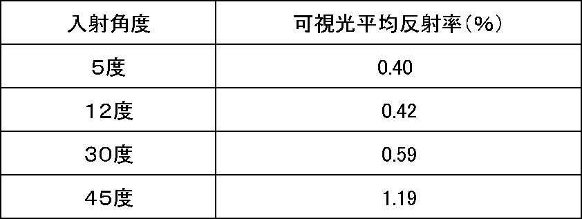
図5及び表2の結果から、5度入射と45度入射の平均反射率は0.80%であり、正面から斜め方向の入射まで広く反射防止できることが分かった。
実施例1において、酸化アルミニウムを厚み58nmに蒸着した代わりに、SiO2を厚み53nmに蒸着した以外は、実施例1と同様にして、実施例2の光学部材を作製した。
得られた光学部材の分光反射率を図5に示した。測定では、表面と裏面の両面からの反射率を測定した。図5中に、5度、12度、30度、及び45度の入射角度における反射率を示した。また、表2に5度、12度、30度、及び45度の入射角度における380nm~780nmの平均反射率を示した。
(実施例3)
実施例2において、沸騰水による水熱処理の時間を20秒間から60分間に変えた以外は、実施例2と同様にして、実施例3の光学部材を作製した。このとき、長時間沸騰水処理をした効果により、最表面の凹凸構造における凸部のアルミナが少しずつ溶出し、凸部の平均高さが50nmまで小さくなった。このときの入射角度と反射率の関係を表3に示す。

表3の結果から、比較例1と比較すると十分な反射防止効果を有していたが、凸部の平均高さが小さくなったので、実施例2と比較すると反射防止性能がやや低下することが分かった。
実施例2において、沸騰水による水熱処理の時間を20秒間から60分間に変えた以外は、実施例2と同様にして、実施例3の光学部材を作製した。このとき、長時間沸騰水処理をした効果により、最表面の凹凸構造における凸部のアルミナが少しずつ溶出し、凸部の平均高さが50nmまで小さくなった。このときの入射角度と反射率の関係を表3に示す。
(実施例4)
実施例2において、水熱処理として沸騰水中に20秒間を、沸騰水中で5分間に変えた以外は、実施例2と同様にして、実施例4の光学部材を作製した。この実施例4の光学部材は、実施例2と同等の性能を有していた。
実施例2において、水熱処理として沸騰水中に20秒間を、沸騰水中で5分間に変えた以外は、実施例2と同様にして、実施例4の光学部材を作製した。この実施例4の光学部材は、実施例2と同等の性能を有していた。
(実施例5)
実施例4において、SiO2を厚み30nmに蒸着し、アルミニウムを厚み10nmに蒸着し、水熱処理として沸騰水中で5分間行った以外は、実施例4と同様にして、実施例5の光学部材を作製した。
得られた光学部材の5度、12度、30度、及び45度の入射角度における380nm~780nmの平均反射率を表4に示す。
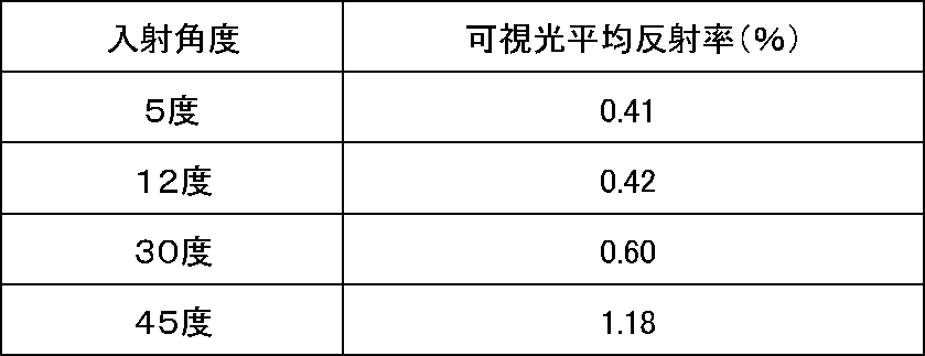
表4の結果から、5度入射と45度入射の平均反射率は0.80%であり、正面から斜め方向の入射まで広く反射防止できることが分かった。
実施例4において、SiO2を厚み30nmに蒸着し、アルミニウムを厚み10nmに蒸着し、水熱処理として沸騰水中で5分間行った以外は、実施例4と同様にして、実施例5の光学部材を作製した。
得られた光学部材の5度、12度、30度、及び45度の入射角度における380nm~780nmの平均反射率を表4に示す。
(実施例6)
実施例2において、水熱処理として沸騰水中に20秒間浸漬を、オートクレーブ処理により2気圧、121℃の水中に20秒間浸漬した以外は、実施例2と同様にして、実施例6の光学部材を作製した。
実施例2において、水熱処理として沸騰水中に20秒間浸漬を、オートクレーブ処理により2気圧、121℃の水中に20秒間浸漬した以外は、実施例2と同様にして、実施例6の光学部材を作製した。
(実施例7)
実施例2において、水熱処理として沸騰水中で20秒間浸漬を、100℃の加熱水蒸気で30分間処理した以外は、実施例2と同様にして、実施例7の光学部材を作製した。
実施例2において、水熱処理として沸騰水中で20秒間浸漬を、100℃の加熱水蒸気で30分間処理した以外は、実施例2と同様にして、実施例7の光学部材を作製した。
(実施例8)
実施例2において、水熱処理として沸騰水中で20秒浸漬を、100℃のアルカリ水溶液(0.5質量%トリエタノールアミン)中で5分間処理した以外は、実施例2と同様にして、実施例8の光学部材を作製した。
得られた光学部材の5度、12度、30度、及び45度の入射角度における380nm~780nmの平均反射率を表5に示す。

表5の結果から、5度入射と45度入射の平均反射率は0.80%であり、正面から斜め方向の入射まで広く反射防止できることが分かった。
実施例2において、水熱処理として沸騰水中で20秒浸漬を、100℃のアルカリ水溶液(0.5質量%トリエタノールアミン)中で5分間処理した以外は、実施例2と同様にして、実施例8の光学部材を作製した。
得られた光学部材の5度、12度、30度、及び45度の入射角度における380nm~780nmの平均反射率を表5に示す。
(実施例9)
実施例2において、アルミニウムを厚み5nmに蒸着する代わりにアルミニウムを厚み120nmに蒸着し、沸騰水処理を10分間行った以外は、実施例2と同様にして、実施例9の光学部材を作製した。
得られた光学部材の5度、12度、30度、及び45度の入射角度における380nm~780nmの平均反射率を表6に示す。
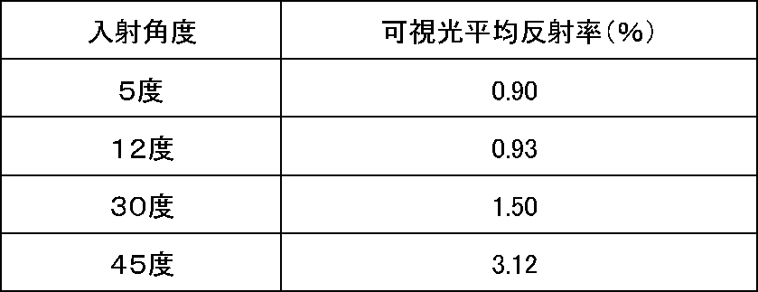
表6の結果から、実施例9の光学部材は、比較例1と比較すると十分な反射防止効果を有していたが、実施例2と比較すると反射防止性能がやや劣ることが分かった。
実施例2において、アルミニウムを厚み5nmに蒸着する代わりにアルミニウムを厚み120nmに蒸着し、沸騰水処理を10分間行った以外は、実施例2と同様にして、実施例9の光学部材を作製した。
得られた光学部材の5度、12度、30度、及び45度の入射角度における380nm~780nmの平均反射率を表6に示す。
(実施例10)
実施例2において、アルミニウムを厚み5nmに蒸着する代わりに酸化アルミニウムを厚み160nmに蒸着し、沸騰水処理を10分間行った以外は、実施例2と同様にして、実施例10の光学部材を作製した。
得られた光学部材の5度、12度、30度、及び45度の入射角度における380nm~780nmの平均反射率を表7に示す。
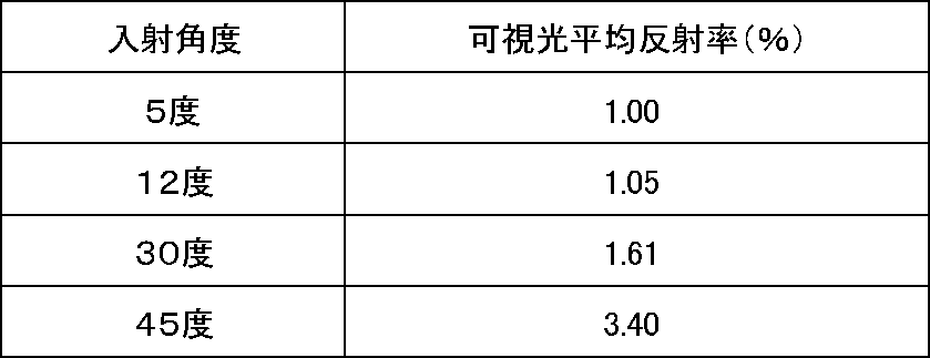
表7の結果から、実施例10の光学部材は、比較例1と比較すると十分な反射防止効果を有していたが、実施例2と比較すると反射防止性能がやや劣ることが分かった。
実施例2において、アルミニウムを厚み5nmに蒸着する代わりに酸化アルミニウムを厚み160nmに蒸着し、沸騰水処理を10分間行った以外は、実施例2と同様にして、実施例10の光学部材を作製した。
得られた光学部材の5度、12度、30度、及び45度の入射角度における380nm~780nmの平均反射率を表7に示す。
(実施例11)
実施例2において、基材としてプラスチック凹メニスカスレンズ(ZEONEX 480R、屈折率1.525)を用い、SiO2を厚みが30nm蒸着し、アルミニウムを厚みが10nm蒸着し、60℃の水中で5分間水熱処理した以外は、実施例2と同様にして、実施例11の光学部材を作製した。実施例11では、ベーマイト単体と比較して、シリカ層が形成されていることにより、水熱処理のプラスチック基材に与える影響が低減されていると考えられる。
得られた光学部材の5度、12度、30度、及び45度の入射角度における380nm~780nmの平均反射率を表8に示す。
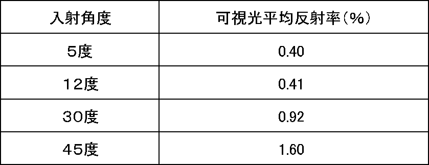
表8の結果から、5度入射と45度入射の平均反射率は1.0%であり、正面から斜め方向の入射まで広く反射防止できることが分かった。
実施例2において、基材としてプラスチック凹メニスカスレンズ(ZEONEX 480R、屈折率1.525)を用い、SiO2を厚みが30nm蒸着し、アルミニウムを厚みが10nm蒸着し、60℃の水中で5分間水熱処理した以外は、実施例2と同様にして、実施例11の光学部材を作製した。実施例11では、ベーマイト単体と比較して、シリカ層が形成されていることにより、水熱処理のプラスチック基材に与える影響が低減されていると考えられる。
得られた光学部材の5度、12度、30度、及び45度の入射角度における380nm~780nmの平均反射率を表8に示す。
(実施例12)
凹メニスカスレンズの凹面が蒸着される配置で、EB蒸着装置(アルバック社製、EBX-8)に設置を行った。200℃に加熱した状態で、真空度2.0×10⁻⁶Torrまで真空引きした。
まず、SiO2を、水晶振動子を参考にして、厚みが24nmになるように電子線ビーム蒸着を行った。次に、ターゲットを切り替えてTiO2を、水晶振動子を参考にして、厚みが16nmになるように電子線ビーム蒸着を行った。
更に、アルミニウム金属を厚みが5nmとなるように蒸着を行った。その後の処理は、実施例1と同様にして、実施例12の光学部材を作製した。
得られた光学部材の分光反射率を図6に示した。測定では、表面と裏面の両面からの反射率を測定した。図6中に、5度、12度、30度、及び45度の入射角度における反射率を示した。また、表9に5度、12度、30度、及び45度の入射角度における380nm~780nmの平均反射率を示した。

図6及び表9の結果から、5度入射と45度入射の平均反射率は0.56%であり、正面から斜め方向の入射まで広く反射防止できることが分かった。
凹メニスカスレンズの凹面が蒸着される配置で、EB蒸着装置(アルバック社製、EBX-8)に設置を行った。200℃に加熱した状態で、真空度2.0×10⁻⁶Torrまで真空引きした。
まず、SiO2を、水晶振動子を参考にして、厚みが24nmになるように電子線ビーム蒸着を行った。次に、ターゲットを切り替えてTiO2を、水晶振動子を参考にして、厚みが16nmになるように電子線ビーム蒸着を行った。
更に、アルミニウム金属を厚みが5nmとなるように蒸着を行った。その後の処理は、実施例1と同様にして、実施例12の光学部材を作製した。
得られた光学部材の分光反射率を図6に示した。測定では、表面と裏面の両面からの反射率を測定した。図6中に、5度、12度、30度、及び45度の入射角度における反射率を示した。また、表9に5度、12度、30度、及び45度の入射角度における380nm~780nmの平均反射率を示した。
(実施例13)
-光学部材の作製-
実施例12において、基材として凹メニスカスレンズを、凹レンズ(材質S-TIH6、オハラ株式会社製)に代えた以外は、実施例12と同様にして、実施例13の光学部材を作製した。
-光学部材の作製-
実施例12において、基材として凹メニスカスレンズを、凹レンズ(材質S-TIH6、オハラ株式会社製)に代えた以外は、実施例12と同様にして、実施例13の光学部材を作製した。
(実施例14)
-光学部材の作製-
実施例12において、基材として凹メニスカスレンズを、凸レンズ(材質S-TIH6、オハラ株式会社製)に代えた以外は、実施例12と同様にして、実施例14の光学部材を作製した。
-光学部材の作製-
実施例12において、基材として凹メニスカスレンズを、凸レンズ(材質S-TIH6、オハラ株式会社製)に代えた以外は、実施例12と同様にして、実施例14の光学部材を作製した。
(実施例15)
-光学部材の作製-
実施例2において、最表層である第2層をAlからAl2O3に代えた以外は、実施例2と同様にして、実施例15の光学部材を作製した。
-光学部材の作製-
実施例2において、最表層である第2層をAlからAl2O3に代えた以外は、実施例2と同様にして、実施例15の光学部材を作製した。
(実施例16)
-光学部材の作製-
実施例12において、最表層である第3層をAlからAl2O3に代えた以外は、実施例12と同様にして、実施例16の光学部材を作製した。
-光学部材の作製-
実施例12において、最表層である第3層をAlからAl2O3に代えた以外は、実施例12と同様にして、実施例16の光学部材を作製した。
(実施例17)
-光学部材の作製-
実施例12において、第1層にAl2O3を厚み60nm、第2層にSiO2を厚み3nm、最表層のアルミニウム厚みを15nmとして、水熱処理時間を20秒間ではなく1分間とした以外は、実施例12と同様にして、実施例17の光学部材を作製した。また、表10に5度、12度、30度、及び45度の入射角度における380nm~780nmの平均反射率を示した。

表10の結果から、5度入射と45度入射の平均反射率は0.31%であり、正面から斜め方向の入射まで広く反射防止できることが分かった。
-光学部材の作製-
実施例12において、第1層にAl2O3を厚み60nm、第2層にSiO2を厚み3nm、最表層のアルミニウム厚みを15nmとして、水熱処理時間を20秒間ではなく1分間とした以外は、実施例12と同様にして、実施例17の光学部材を作製した。また、表10に5度、12度、30度、及び45度の入射角度における380nm~780nmの平均反射率を示した。
(実施例18)
-光学部材の作製-
実施例17において、水熱処理時間を1分間ではなく5分間行った以外は、実施例17と同様にして、実施例18の光学部材を作製した。
得られた光学部材は、下層に酸化アルミニウムが存在し、実施例17と水熱処理時間を変化させたにもかかわらず、同様の光学特性が得られた。誘電体層(SiO2層)の耐透湿性及び耐透水性の効果により水熱処理に対する安定性が得られることが分かった。
-光学部材の作製-
実施例17において、水熱処理時間を1分間ではなく5分間行った以外は、実施例17と同様にして、実施例18の光学部材を作製した。
得られた光学部材は、下層に酸化アルミニウムが存在し、実施例17と水熱処理時間を変化させたにもかかわらず、同様の光学特性が得られた。誘電体層(SiO2層)の耐透湿性及び耐透水性の効果により水熱処理に対する安定性が得られることが分かった。
(実施例19)
-光学部材の作製-
実施例1において、各層の形成をEB蒸着(非連続)で行った以外は、実施例1と同様にして、実施例19の光学部材を作製した。
-光学部材の作製-
実施例1において、各層の形成をEB蒸着(非連続)で行った以外は、実施例1と同様にして、実施例19の光学部材を作製した。
(実施例20)
-光学部材の作製-
実施例2において、各層の形成をEB蒸着(非連続)で行った以外は、実施例2と同様にして、実施例20の光学部材を作製した。
-光学部材の作製-
実施例2において、各層の形成をEB蒸着(非連続)で行った以外は、実施例2と同様にして、実施例20の光学部材を作製した。
(実施例21)
-光学部材の作製-
実施例12において、各層の形成をEB蒸着(非連続)で行った以外は、実施例12と同様にして、実施例21の光学部材を作製した。
-光学部材の作製-
実施例12において、各層の形成をEB蒸着(非連続)で行った以外は、実施例12と同様にして、実施例21の光学部材を作製した。
(実施例22)
-光学部材の作製-
実施例1において、酸化アルミニウムを厚み58nmに蒸着する代わりに、酸化アルミニウムを厚み39nm、酸化ジルコニウムを厚み9nm、SiO2を厚み15nmにそれぞれ蒸着した以外は、実施例1と同様にして、実施例22の光学部材を作製した。
得られた光学部材の5度、12度、30度、及び45度の入射角度における380nm~780nmの平均反射率を表11に示す。

表11の結果から、5度入射と45度入射の平均反射率は0.13%であり、正面から斜め方向の入射まで広く反射防止できることが分かった。
-光学部材の作製-
実施例1において、酸化アルミニウムを厚み58nmに蒸着する代わりに、酸化アルミニウムを厚み39nm、酸化ジルコニウムを厚み9nm、SiO2を厚み15nmにそれぞれ蒸着した以外は、実施例1と同様にして、実施例22の光学部材を作製した。
得られた光学部材の5度、12度、30度、及び45度の入射角度における380nm~780nmの平均反射率を表11に示す。
(実施例23)
-光学部材の作製-
実施例22において、水熱処理として沸騰水中で20秒間を、沸騰水中で5分間処理した以外は、実施例22と同様にして、実施例23の光学部材を作製した。
得られた光学部材は、実施例22と同等の光学特性が得られた。このことから、下層に酸化アルミニウム層があっても、誘電体層の耐透湿性及び耐透水性の効果により水熱処理に対する安定性が得られることが分かった。
-光学部材の作製-
実施例22において、水熱処理として沸騰水中で20秒間を、沸騰水中で5分間処理した以外は、実施例22と同様にして、実施例23の光学部材を作製した。
得られた光学部材は、実施例22と同等の光学特性が得られた。このことから、下層に酸化アルミニウム層があっても、誘電体層の耐透湿性及び耐透水性の効果により水熱処理に対する安定性が得られることが分かった。
(実施例24)
-光学部材の作製-
実施例1において、酸化アルミニウムを厚み58nmに蒸着する代わりに、SiO2を厚み20nm、酸化ジルコニウムを厚み17nm、SiO2を厚み19nmに、ぞれぞれ蒸着した以外は、実施例1と同様にして、実施例24の光学部材を作製した。
得られた光学部材の5度、12度、30度、及び45度の入射角度における380nm~780nmの平均反射率を表12に示す。

表12の結果から、5度入射と45度入射の平均反射率は0.15%であり、正面から斜め方向の入射まで広く反射防止できることが分かった。
-光学部材の作製-
実施例1において、酸化アルミニウムを厚み58nmに蒸着する代わりに、SiO2を厚み20nm、酸化ジルコニウムを厚み17nm、SiO2を厚み19nmに、ぞれぞれ蒸着した以外は、実施例1と同様にして、実施例24の光学部材を作製した。
得られた光学部材の5度、12度、30度、及び45度の入射角度における380nm~780nmの平均反射率を表12に示す。
(比較例1)
-光学部材の作製-
実施例1において、凹メニスカスレンズにアルミニウム蒸着膜を形成しない以外は、実施例1と同様にして、比較例1の光学部材を作製した。
-光学部材の作製-
実施例1において、凹メニスカスレンズにアルミニウム蒸着膜を形成しない以外は、実施例1と同様にして、比較例1の光学部材を作製した。
(比較例2)
-光学部材の作製-
比較例2として、基材として平面ガラス(材質S-TIH6、オハラ株式会社製)を用い、特許第4182236号公報の実施例2を再現した光学部材を作製した。
-光学部材の作製-
比較例2として、基材として平面ガラス(材質S-TIH6、オハラ株式会社製)を用い、特許第4182236号公報の実施例2を再現した光学部材を作製した。
(比較例3)
-光学部材の作製-
比較例3として、基材として凹メニスカスレンズを用い、特許第4182236号公報の実施例2を再現した光学部材を作製した。
このレンズは、凸部においてレンズ縁の方が中央部より膜厚が厚くなる現象が見られ、レンズの各部位によって反射率が異なるという現象が見られた。このような現象は、「第35回光学シンポジウム講演予稿集p67のFig2」に記載されている。
得られたレンズについて、実施例1と同様にして380nm~780nmの平均反射率の測定を行った。その結果、5度入射光の反射率と45度入射光の反射率が大きく異なることが分かった。
-光学部材の作製-
比較例3として、基材として凹メニスカスレンズを用い、特許第4182236号公報の実施例2を再現した光学部材を作製した。
このレンズは、凸部においてレンズ縁の方が中央部より膜厚が厚くなる現象が見られ、レンズの各部位によって反射率が異なるという現象が見られた。このような現象は、「第35回光学シンポジウム講演予稿集p67のFig2」に記載されている。
得られたレンズについて、実施例1と同様にして380nm~780nmの平均反射率の測定を行った。その結果、5度入射光の反射率と45度入射光の反射率が大きく異なることが分かった。
(比較例4)
-光学部材の作製-
実施例2において、誘電体層であるSiO2の蒸着を行わずに、アルミニウム5nmの蒸着のみを行った以外は、実施例2と同様にして、比較例4の光学部材を作製した。
得られた光学部材は、反射防止効果が十分得られなかった。
-光学部材の作製-
実施例2において、誘電体層であるSiO2の蒸着を行わずに、アルミニウム5nmの蒸着のみを行った以外は、実施例2と同様にして、比較例4の光学部材を作製した。
得られた光学部材は、反射防止効果が十分得られなかった。
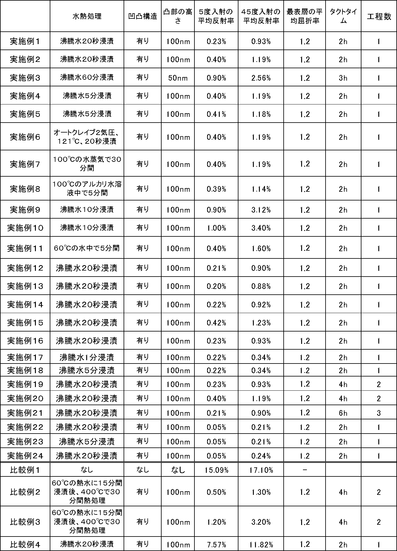
次に、実施例1~24及び比較例1~4について、製造条件及び評価結果を表13にまとめて示す。
<タクトタイムの測定>
真空蒸着については真空を破ってサンプルをセットする時点から、蒸着が終了し、サンプルを取り出すまでの時間を測定した。この間、真空度が目標に達成するまでの待ち時間がほとんどであった。水熱処理については、サンプルの治具への準備を開始時間として、サンプルの乾燥終了を終了時間として計測した。結果を表13-2に示す。
真空蒸着については真空を破ってサンプルをセットする時点から、蒸着が終了し、サンプルを取り出すまでの時間を測定した。この間、真空度が目標に達成するまでの待ち時間がほとんどであった。水熱処理については、サンプルの治具への準備を開始時間として、サンプルの乾燥終了を終了時間として計測した。結果を表13-2に示す。

本発明の光学部材は、例えば、ガラス眼鏡、カメラレンズ、光学レンズ、太陽電池パネル、ブラウン管、フィルター、ワープロ、コンピュータ、液晶テレビ、プラズマディスプレイパネル等のディスプレイ、液晶表示装置に用いる偏光板、カメラ用ファインダーレンズ、プリズム、フライアイレンズ、トーリックレンズ、各種計器のカバー、自動車、電車等の窓ガラス、プロジェクター用レンズ、光学センサー等に用いられるマイクロレンズなどに好適に用いられる。
本発明の態様としては以下のとおりである。
<1> 少なくとも一部に曲面を有する基材と、該基材上に、アルミニウム単体、及びアルミニウムを含む化合物の少なくともいずれかを気相成膜した層を水熱処理して最表面に凹凸構造を有してなり、
前記基材と前記凹凸構造の間に、気相成膜により形成された誘電体層を有することを特徴とする光学部材である。
<2> アルミニウム単体、及びアルミニウムを含む化合物の少なくともいずれかを気相成膜した層が、アルミニウム及びアルミナの少なくともいずれかからなる前記<1>に記載の光学部材である。
<3> 水熱処理が60℃以上沸騰温度以下の温水及び60℃以上沸騰温度以下のアルカリ水溶液のいずれかに浸漬する処理である前記<1>から<2>のいずれかに記載の光学部材である。
<4> 水熱処理が水蒸気にさらす処理である前記<1>から<2>のいずれかに記載の光学部材である。
<5> 凹凸構造における凸部の平均高さが5nm~1,000nmである前記<1>から<4>のいずれかに記載の光学部材である。
<6> 気相成膜されたアルミニウムからなる最表層の水熱処理前の平均厚みが100nm以下である前記<2>から<5>のいずれかに記載の光学部材である。
<7> 気相成膜されたアルミナからなる最表層の水熱処理前の平均厚みが150nm以下である前記<2>から<5>のいずれかに記載の光学部材である。
<8> 誘電体層が2層以上からなる誘電体多層膜である前記<1>から<7>のいずれかに記載の光学部材である。
<9> 基材が、曲率を有するレンズである前記<1>から<8>のいずれかに記載の光学部材である。
<10> 少なくとも一部に曲面を有する基材上に、気相成膜により誘電体層を形成する誘電体層形成工程と、
前記誘電体層上にアルミニウム単体、及びアルミニウムを含む化合物の少なくともいずれかを気相成膜により最表層を形成する最表層形成工程と、
最表層を水熱処理して凹凸構造を形成する水熱処理工程と、
を含むことを特徴とする光学部材の製造方法である。
<11> 誘電体層形成工程及び最表層形成工程の気相成膜を、真空状態を維持したまま連続で行う前記<10>に記載の光学部材の製造方法である。
<1> 少なくとも一部に曲面を有する基材と、該基材上に、アルミニウム単体、及びアルミニウムを含む化合物の少なくともいずれかを気相成膜した層を水熱処理して最表面に凹凸構造を有してなり、
前記基材と前記凹凸構造の間に、気相成膜により形成された誘電体層を有することを特徴とする光学部材である。
<2> アルミニウム単体、及びアルミニウムを含む化合物の少なくともいずれかを気相成膜した層が、アルミニウム及びアルミナの少なくともいずれかからなる前記<1>に記載の光学部材である。
<3> 水熱処理が60℃以上沸騰温度以下の温水及び60℃以上沸騰温度以下のアルカリ水溶液のいずれかに浸漬する処理である前記<1>から<2>のいずれかに記載の光学部材である。
<4> 水熱処理が水蒸気にさらす処理である前記<1>から<2>のいずれかに記載の光学部材である。
<5> 凹凸構造における凸部の平均高さが5nm~1,000nmである前記<1>から<4>のいずれかに記載の光学部材である。
<6> 気相成膜されたアルミニウムからなる最表層の水熱処理前の平均厚みが100nm以下である前記<2>から<5>のいずれかに記載の光学部材である。
<7> 気相成膜されたアルミナからなる最表層の水熱処理前の平均厚みが150nm以下である前記<2>から<5>のいずれかに記載の光学部材である。
<8> 誘電体層が2層以上からなる誘電体多層膜である前記<1>から<7>のいずれかに記載の光学部材である。
<9> 基材が、曲率を有するレンズである前記<1>から<8>のいずれかに記載の光学部材である。
<10> 少なくとも一部に曲面を有する基材上に、気相成膜により誘電体層を形成する誘電体層形成工程と、
前記誘電体層上にアルミニウム単体、及びアルミニウムを含む化合物の少なくともいずれかを気相成膜により最表層を形成する最表層形成工程と、
最表層を水熱処理して凹凸構造を形成する水熱処理工程と、
を含むことを特徴とする光学部材の製造方法である。
<11> 誘電体層形成工程及び最表層形成工程の気相成膜を、真空状態を維持したまま連続で行う前記<10>に記載の光学部材の製造方法である。
Claims (11)
- 少なくとも一部に曲面を有する基材と、該基材上に、アルミニウム単体、及びアルミニウムを含む化合物の少なくともいずれかを気相成膜した層を水熱処理して最表面に凹凸構造を有してなり、
前記基材と前記凹凸構造の間に、気相成膜により形成された誘電体層を有することを特徴とする光学部材。 - アルミニウム単体、及びアルミニウムを含む化合物の少なくともいずれかを気相成膜した層が、アルミニウム及びアルミナの少なくともいずれかからなる請求項1に記載の光学部材。
- 水熱処理が60℃以上沸騰温度以下の温水及び60℃以上沸騰温度以下のアルカリ水溶液のいずれかに浸漬する処理である請求項1から2のいずれかに記載の光学部材。
- 水熱処理が水蒸気にさらす処理である請求項1から2のいずれかに記載の光学部材。
- 凹凸構造における凸部の平均高さが5nm~1,000nmである請求項1から4のいずれかに記載の光学部材。
- 気相成膜されたアルミニウムからなる最表層の水熱処理前の平均厚みが100nm以下である請求項2から5のいずれかに記載の光学部材。
- 気相成膜されたアルミナからなる最表層の水熱処理前の平均厚みが150nm以下である請求項2から5のいずれかに記載の光学部材。
- 誘電体層が2層以上からなる誘電体多層膜である請求項1から7のいずれかに記載の光学部材。
- 基材が、曲率を有するレンズである請求項1から8のいずれかに記載の光学部材。
- 少なくとも一部に曲面を有する基材上に、気相成膜により誘電体層を形成する誘電体層形成工程と、
前記誘電体層上にアルミニウム単体、及びアルミニウムを含む化合物の少なくともいずれかを気相成膜により最表層を形成する最表層形成工程と、
最表層を水熱処理して凹凸構造を形成する水熱処理工程と、
を含むことを特徴とする光学部材の製造方法。 - 誘電体層形成工程及び最表層形成工程の気相成膜を、真空状態を維持したまま連続で行う請求項10に記載の光学部材の製造方法。
Priority Applications (3)
| Application Number | Priority Date | Filing Date | Title |
|---|---|---|---|
| EP11861466.8A EP2687875B1 (en) | 2011-03-18 | 2011-12-15 | Method for producing optical member |
| CN2011800692609A CN103443662A (zh) | 2011-03-18 | 2011-12-15 | 光学部件及其制造方法 |
| US14/028,992 US9459379B2 (en) | 2011-03-18 | 2013-09-17 | Optical member and method for producing same |
Applications Claiming Priority (2)
| Application Number | Priority Date | Filing Date | Title |
|---|---|---|---|
| JP2011061404A JP5647924B2 (ja) | 2011-03-18 | 2011-03-18 | 光学部材の製造方法 |
| JP2011-061404 | 2011-03-18 |
Related Child Applications (1)
| Application Number | Title | Priority Date | Filing Date |
|---|---|---|---|
| US14/028,992 Continuation US9459379B2 (en) | 2011-03-18 | 2013-09-17 | Optical member and method for producing same |
Publications (1)
| Publication Number | Publication Date |
|---|---|
| WO2012127744A1 true WO2012127744A1 (ja) | 2012-09-27 |
Family
ID=46878932
Family Applications (1)
| Application Number | Title | Priority Date | Filing Date |
|---|---|---|---|
| PCT/JP2011/079017 Ceased WO2012127744A1 (ja) | 2011-03-18 | 2011-12-15 | 光学部材及びその製造方法 |
Country Status (5)
| Country | Link |
|---|---|
| US (1) | US9459379B2 (ja) |
| EP (1) | EP2687875B1 (ja) |
| JP (1) | JP5647924B2 (ja) |
| CN (1) | CN103443662A (ja) |
| WO (1) | WO2012127744A1 (ja) |
Cited By (3)
| Publication number | Priority date | Publication date | Assignee | Title |
|---|---|---|---|---|
| JP2014081522A (ja) * | 2012-10-17 | 2014-05-08 | Fujifilm Corp | 反射防止膜を備えた光学部材およびその製造方法 |
| JP2014098885A (ja) * | 2012-10-17 | 2014-05-29 | Fujifilm Corp | 反射防止膜を備えた光学部材およびその製造方法 |
| WO2019208366A1 (ja) * | 2018-04-26 | 2019-10-31 | 富士フイルム株式会社 | 光学薄膜、光学素子、光学系および光学薄膜の製造方法 |
Families Citing this family (29)
| Publication number | Priority date | Publication date | Assignee | Title |
|---|---|---|---|---|
| JP5885649B2 (ja) * | 2012-12-20 | 2016-03-15 | キヤノン株式会社 | 反射防止膜を有する光学素子、光学系および光学機器 |
| JP6313941B2 (ja) * | 2013-08-30 | 2018-04-18 | Hoya株式会社 | 眼鏡レンズ |
| JP6234753B2 (ja) * | 2013-09-17 | 2017-11-22 | 富士フイルム株式会社 | 透明微細凹凸構造体の製造方法 |
| JP2015114381A (ja) * | 2013-12-09 | 2015-06-22 | 東京エレクトロン株式会社 | 反射防止機能を有する部材およびその製造方法 |
| JP6234857B2 (ja) * | 2014-03-24 | 2017-11-22 | 富士フイルム株式会社 | 反射防止機能付きレンズの製造方法 |
| JP6411517B2 (ja) | 2014-08-25 | 2018-10-24 | 富士フイルム株式会社 | 反射防止膜および反射防止膜を備えた光学部材 |
| WO2016031133A1 (ja) * | 2014-08-27 | 2016-03-03 | 富士フイルム株式会社 | 反射防止膜を備えた光学部材およびその製造方法 |
| JP6338503B2 (ja) * | 2014-09-30 | 2018-06-06 | 富士フイルム株式会社 | 光学素子および光学素子の製造方法 |
| JP6505736B2 (ja) * | 2014-10-15 | 2019-04-24 | 富士フイルム株式会社 | 光学素子および光学素子の製造方法 |
| WO2016068423A1 (ko) * | 2014-11-01 | 2016-05-06 | 삼성에스디아이 주식회사 | 플렉시블 디스플레이 장치 |
| WO2016136261A1 (ja) | 2015-02-27 | 2016-09-01 | 富士フイルム株式会社 | 反射防止膜および光学部材 |
| DE112016000959T5 (de) * | 2015-02-27 | 2017-11-09 | Fujifilm Corporation | Antireflexfilm und Verfahren zu dessen Herstellung und optisches Bauelement |
| WO2016159290A1 (ja) | 2015-03-31 | 2016-10-06 | 富士フイルム株式会社 | 反射防止膜及びその製造方法 |
| JP6266840B2 (ja) * | 2015-04-20 | 2018-01-24 | 富士フイルム株式会社 | 構造物の製造方法 |
| CN105236756A (zh) * | 2015-09-21 | 2016-01-13 | 海南大学 | 减反射玻璃及其制备方法 |
| JP2017151200A (ja) * | 2016-02-23 | 2017-08-31 | コニカミノルタ株式会社 | 反射防止体の製造方法 |
| JP6476347B2 (ja) | 2016-03-09 | 2019-02-27 | エルジー・ケム・リミテッド | 反射防止フィルム |
| CN109196388A (zh) * | 2017-03-13 | 2019-01-11 | 京东方科技集团股份有限公司 | 抗反射涂层、触控基板、显示装置和制造抗反射涂层的方法 |
| JP2018159884A (ja) * | 2017-03-23 | 2018-10-11 | 三好興業株式会社 | 半透明レンズ、サングラス及び半透明レンズの製造方法 |
| US11143800B2 (en) * | 2017-06-16 | 2021-10-12 | Corning Incorporated | Extending the reflection bandwith of silver coating stacks for highly reflective mirrors |
| JP6918208B2 (ja) * | 2018-03-29 | 2021-08-11 | 富士フイルム株式会社 | 反射防止膜および光学部材 |
| CN108642447A (zh) * | 2018-05-08 | 2018-10-12 | 北京汉能光伏投资有限公司 | 一种曲面镀膜板及其制备方法和包含其的太阳能组件 |
| CN112213803A (zh) * | 2020-11-13 | 2021-01-12 | 光驰科技(上海)有限公司 | 一种防水光学薄膜及制作方法 |
| JP7274799B2 (ja) * | 2021-02-08 | 2023-05-17 | 東海光学株式会社 | 光学製品 |
| JP7055494B1 (ja) | 2021-02-08 | 2022-04-18 | 東海光学株式会社 | 光学製品の製造方法 |
| WO2023047948A1 (ja) * | 2021-09-24 | 2023-03-30 | 東海光学株式会社 | 光学製品及び光学製品の製造方法 |
| CN113985504B (zh) * | 2021-12-27 | 2022-04-26 | 诚瑞光学(苏州)有限公司 | 光学镜片 |
| JP2024085500A (ja) * | 2022-12-15 | 2024-06-27 | キヤノン株式会社 | 光学素子、結像光学系および光学機器 |
| FI20245571A1 (en) * | 2024-05-08 | 2025-11-09 | Beneq Oy | An anti-reflective coating on a surface of a substrate |
Citations (7)
| Publication number | Priority date | Publication date | Assignee | Title |
|---|---|---|---|---|
| JPS6148124B2 (ja) | 1977-02-18 | 1986-10-22 | Minnesota Mining & Mfg | |
| JP2006259711A (ja) * | 2005-02-18 | 2006-09-28 | Canon Inc | 光学用透明部材及びそれを用いた光学系 |
| JP2006297681A (ja) * | 2005-04-19 | 2006-11-02 | Japan Vilene Co Ltd | 透明性材料及びその製造方法 |
| JP2007213780A (ja) * | 2006-01-11 | 2007-08-23 | Pentax Corp | 反射防止膜を有する光学素子 |
| JP4182236B2 (ja) | 2004-02-23 | 2008-11-19 | キヤノン株式会社 | 光学部材および光学部材の製造方法 |
| JP2009139775A (ja) * | 2007-12-10 | 2009-06-25 | Canon Inc | 光学系及びそれを有する光学機器 |
| JP2009217049A (ja) * | 2008-03-11 | 2009-09-24 | Hoya Corp | 顕微鏡対物レンズおよび顕微鏡 |
Family Cites Families (5)
| Publication number | Priority date | Publication date | Assignee | Title |
|---|---|---|---|---|
| US6896981B2 (en) * | 2001-07-24 | 2005-05-24 | Bridgestone Corporation | Transparent conductive film and touch panel |
| CN100595608C (zh) * | 2005-02-18 | 2010-03-24 | 佳能株式会社 | 光学透明部件和使用该光学透明部件的光学系统 |
| TW200746123A (en) | 2006-01-11 | 2007-12-16 | Pentax Corp | Optical element having anti-reflection coating |
| JP4639241B2 (ja) * | 2007-02-20 | 2011-02-23 | キヤノン株式会社 | 光学用部材、それを用いた光学系及び光学用部材の製造方法 |
| JP5279344B2 (ja) * | 2007-06-06 | 2013-09-04 | キヤノン株式会社 | 光学素子の製造方法 |
-
2011
- 2011-03-18 JP JP2011061404A patent/JP5647924B2/ja active Active
- 2011-12-15 WO PCT/JP2011/079017 patent/WO2012127744A1/ja not_active Ceased
- 2011-12-15 CN CN2011800692609A patent/CN103443662A/zh active Pending
- 2011-12-15 EP EP11861466.8A patent/EP2687875B1/en not_active Not-in-force
-
2013
- 2013-09-17 US US14/028,992 patent/US9459379B2/en active Active
Patent Citations (7)
| Publication number | Priority date | Publication date | Assignee | Title |
|---|---|---|---|---|
| JPS6148124B2 (ja) | 1977-02-18 | 1986-10-22 | Minnesota Mining & Mfg | |
| JP4182236B2 (ja) | 2004-02-23 | 2008-11-19 | キヤノン株式会社 | 光学部材および光学部材の製造方法 |
| JP2006259711A (ja) * | 2005-02-18 | 2006-09-28 | Canon Inc | 光学用透明部材及びそれを用いた光学系 |
| JP2006297681A (ja) * | 2005-04-19 | 2006-11-02 | Japan Vilene Co Ltd | 透明性材料及びその製造方法 |
| JP2007213780A (ja) * | 2006-01-11 | 2007-08-23 | Pentax Corp | 反射防止膜を有する光学素子 |
| JP2009139775A (ja) * | 2007-12-10 | 2009-06-25 | Canon Inc | 光学系及びそれを有する光学機器 |
| JP2009217049A (ja) * | 2008-03-11 | 2009-09-24 | Hoya Corp | 顕微鏡対物レンズおよび顕微鏡 |
Non-Patent Citations (1)
| Title |
|---|
| See also references of EP2687875A4 * |
Cited By (3)
| Publication number | Priority date | Publication date | Assignee | Title |
|---|---|---|---|---|
| JP2014081522A (ja) * | 2012-10-17 | 2014-05-08 | Fujifilm Corp | 反射防止膜を備えた光学部材およびその製造方法 |
| JP2014098885A (ja) * | 2012-10-17 | 2014-05-29 | Fujifilm Corp | 反射防止膜を備えた光学部材およびその製造方法 |
| WO2019208366A1 (ja) * | 2018-04-26 | 2019-10-31 | 富士フイルム株式会社 | 光学薄膜、光学素子、光学系および光学薄膜の製造方法 |
Also Published As
| Publication number | Publication date |
|---|---|
| JP2012198330A (ja) | 2012-10-18 |
| JP5647924B2 (ja) | 2015-01-07 |
| EP2687875B1 (en) | 2016-11-30 |
| CN103443662A (zh) | 2013-12-11 |
| US20140016204A1 (en) | 2014-01-16 |
| US9459379B2 (en) | 2016-10-04 |
| EP2687875A4 (en) | 2014-11-05 |
| EP2687875A1 (en) | 2014-01-22 |
Similar Documents
| Publication | Publication Date | Title |
|---|---|---|
| JP5647924B2 (ja) | 光学部材の製造方法 | |
| JP5622468B2 (ja) | レンズの製造方法及びレンズ | |
| TWI588112B (zh) | 用於製造具光學及易於清潔之塗層的玻璃製品之製程 | |
| CN105143930B (zh) | 用于高反射镜子的增强、耐用银涂层堆叠 | |
| CN101726767A (zh) | 光学物品及其制造方法 | |
| CN102645681B (zh) | 光学部件、其制造方法以及使用其的光学系统 | |
| JP3808917B2 (ja) | 薄膜の製造方法及び薄膜 | |
| JP2011013654A (ja) | 多層反射防止層およびその製造方法、プラスチックレンズ | |
| JP5698902B2 (ja) | 光学物品およびその製造方法 | |
| CN101639558A (zh) | 镜头、去除镜头眩光的方法及制造镜筒的模具 | |
| CN112005131A (zh) | 光学薄膜、光学构件及光学薄膜的制造方法 | |
| JPWO2002018981A1 (ja) | 光学薄膜の形成方法 | |
| CN110262079A (zh) | 一种埃米抗氧化渐进多彩镜片及其制备方法 | |
| CN113985504B (zh) | 光学镜片 | |
| JP2009217018A (ja) | 光学物品及び光学物品の製造方法 | |
| JP7065995B2 (ja) | 反射防止膜の製造方法、および微細凹凸構造の形成方法 | |
| CN110709364A (zh) | 带有亲水性防反射膜的透镜及其制造方法 | |
| JP2011017949A (ja) | 光学物品の製造方法およびその方法により製造された光学物品 | |
| JP2019066600A (ja) | プラスチックレンズ及びその製造方法 | |
| JP2010072635A (ja) | 光学物品およびその製造方法 | |
| JP2010072636A (ja) | 光学物品およびその製造方法 | |
| TWI923844B (zh) | 光學積層體及抗反射膜 | |
| JP2009093067A (ja) | 酸化ジルコニウム層、耐擦傷性物品および光学物品 | |
| JP2009093068A (ja) | 耐擦傷性物品の製造方法 | |
| JP2019020721A (ja) | Ndフィルタ及びその製造方法 |
Legal Events
| Date | Code | Title | Description |
|---|---|---|---|
| 121 | Ep: the epo has been informed by wipo that ep was designated in this application |
Ref document number: 11861466 Country of ref document: EP Kind code of ref document: A1 |
|
| NENP | Non-entry into the national phase |
Ref country code: DE |
|
| REEP | Request for entry into the european phase |
Ref document number: 2011861466 Country of ref document: EP |
|
| WWE | Wipo information: entry into national phase |
Ref document number: 2011861466 Country of ref document: EP |