WO2012137958A1 - 有機化合物、電荷輸送材料、該化合物を含有する組成物、有機電界発光素子、表示装置及び照明装置 - Google Patents
有機化合物、電荷輸送材料、該化合物を含有する組成物、有機電界発光素子、表示装置及び照明装置 Download PDFInfo
- Publication number
- WO2012137958A1 WO2012137958A1 PCT/JP2012/059600 JP2012059600W WO2012137958A1 WO 2012137958 A1 WO2012137958 A1 WO 2012137958A1 JP 2012059600 W JP2012059600 W JP 2012059600W WO 2012137958 A1 WO2012137958 A1 WO 2012137958A1
- Authority
- WO
- WIPO (PCT)
- Prior art keywords
- group
- compound
- substituent
- organic
- ring
- Prior art date
- Legal status (The legal status is an assumption and is not a legal conclusion. Google has not performed a legal analysis and makes no representation as to the accuracy of the status listed.)
- Ceased
Links
- 0 CCCCCC(CC1)NC1C(C(CC1)C(C)C(*2)C2=*)C=C1C1CCCCC1 Chemical compound CCCCCC(CC1)NC1C(C(CC1)C(C)C(*2)C2=*)C=C1C1CCCCC1 0.000 description 17
- NXGFNFLNQTUAPJ-UHFFFAOYSA-N C(C(c1cc(-[n]2c3ccccc3c3c2cccc3)ccc1)NC(c1cc(-[n]2c3ccccc3c3c2cccc3)ccc1)=C1)=C1c(cc1)ccc1-c1ccccc1 Chemical compound C(C(c1cc(-[n]2c3ccccc3c3c2cccc3)ccc1)NC(c1cc(-[n]2c3ccccc3c3c2cccc3)ccc1)=C1)=C1c(cc1)ccc1-c1ccccc1 NXGFNFLNQTUAPJ-UHFFFAOYSA-N 0.000 description 1
- IGRVWUTTWUZBRE-UHFFFAOYSA-N CN1C(C2=CC=CCC2c2cccc(-c3ccccc3)c2)=NC(c2cccc(-[n]3c4ccccc4c4c3cccc4)c2)=NC1c(cc1)ccc1-c1cc(-c2ccccc2)ccc1 Chemical compound CN1C(C2=CC=CCC2c2cccc(-c3ccccc3)c2)=NC(c2cccc(-[n]3c4ccccc4c4c3cccc4)c2)=NC1c(cc1)ccc1-c1cc(-c2ccccc2)ccc1 IGRVWUTTWUZBRE-UHFFFAOYSA-N 0.000 description 1
- RBFHUDLXKROWKT-UHFFFAOYSA-N C[Si](C)(c1ccccn1)O Chemical compound C[Si](C)(c1ccccn1)O RBFHUDLXKROWKT-UHFFFAOYSA-N 0.000 description 1
- SMUQFGGVLNAIOZ-UHFFFAOYSA-N Cc1nc2ccccc2cc1 Chemical compound Cc1nc2ccccc2cc1 SMUQFGGVLNAIOZ-UHFFFAOYSA-N 0.000 description 1
- FFDQAQBDOJUCRU-UHFFFAOYSA-N Clc1cc(-c(cc2)ccc2-c2cc(-c3cccc(-c4ccccc4)c3)ccc2)nc(Cl)n1 Chemical compound Clc1cc(-c(cc2)ccc2-c2cc(-c3cccc(-c4ccccc4)c3)ccc2)nc(Cl)n1 FFDQAQBDOJUCRU-UHFFFAOYSA-N 0.000 description 1
- QBCZPKGKIZXZHP-UHFFFAOYSA-N Clc1nc(-c(cc2)ccc2-c2cccc(-c3ccccc3)c2)cc(-c(cc2)ccc2-c2cccc(-c3cc(-c4ccccc4)ccc3)c2)n1 Chemical compound Clc1nc(-c(cc2)ccc2-c2cccc(-c3ccccc3)c2)cc(-c(cc2)ccc2-c2cccc(-c3cc(-c4ccccc4)ccc3)c2)n1 QBCZPKGKIZXZHP-UHFFFAOYSA-N 0.000 description 1
- LNPNTLQWZHXPTQ-UHFFFAOYSA-N Clc1nc(-c2cc(-[n]3c(cccc4)c4c4c3cccc4)ccc2)nc(-c(cc2)ccc2-c2cccc(-c3ccccc3)c2)n1 Chemical compound Clc1nc(-c2cc(-[n]3c(cccc4)c4c4c3cccc4)ccc2)nc(-c(cc2)ccc2-c2cccc(-c3ccccc3)c2)n1 LNPNTLQWZHXPTQ-UHFFFAOYSA-N 0.000 description 1
- LGLLLSXCRNWFKJ-UHFFFAOYSA-N OC(C1=[N]=CC=C1)=O Chemical compound OC(C1=[N]=CC=C1)=O LGLLLSXCRNWFKJ-UHFFFAOYSA-N 0.000 description 1
- RBPYQUPJYARESA-UHFFFAOYSA-N c(cc1)ccc1-c1cc(-c(cc2)ccc2-c2nc(-c3cc(-[n]4c(cccc5)c5c5c4cccc5)ccc3)nc(-c3cccc(-[n]4c(cccc5)c5c5c4cccc5)c3)n2)ccc1 Chemical compound c(cc1)ccc1-c1cc(-c(cc2)ccc2-c2nc(-c3cc(-[n]4c(cccc5)c5c5c4cccc5)ccc3)nc(-c3cccc(-[n]4c(cccc5)c5c5c4cccc5)c3)n2)ccc1 RBPYQUPJYARESA-UHFFFAOYSA-N 0.000 description 1
Images

Classifications
-
- C—CHEMISTRY; METALLURGY
- C07—ORGANIC CHEMISTRY
- C07D—HETEROCYCLIC COMPOUNDS
- C07D251/00—Heterocyclic compounds containing 1,3,5-triazine rings
- C07D251/02—Heterocyclic compounds containing 1,3,5-triazine rings not condensed with other rings
- C07D251/12—Heterocyclic compounds containing 1,3,5-triazine rings not condensed with other rings having three double bonds between ring members or between ring members and non-ring members
- C07D251/14—Heterocyclic compounds containing 1,3,5-triazine rings not condensed with other rings having three double bonds between ring members or between ring members and non-ring members with hydrogen or carbon atoms directly attached to at least one ring carbon atom
- C07D251/24—Heterocyclic compounds containing 1,3,5-triazine rings not condensed with other rings having three double bonds between ring members or between ring members and non-ring members with hydrogen or carbon atoms directly attached to at least one ring carbon atom to three ring carbon atoms
-
- C—CHEMISTRY; METALLURGY
- C07—ORGANIC CHEMISTRY
- C07D—HETEROCYCLIC COMPOUNDS
- C07D239/00—Heterocyclic compounds containing 1,3-diazine or hydrogenated 1,3-diazine rings
- C07D239/02—Heterocyclic compounds containing 1,3-diazine or hydrogenated 1,3-diazine rings not condensed with other rings
- C07D239/24—Heterocyclic compounds containing 1,3-diazine or hydrogenated 1,3-diazine rings not condensed with other rings having three or more double bonds between ring members or between ring members and non-ring members
- C07D239/26—Heterocyclic compounds containing 1,3-diazine or hydrogenated 1,3-diazine rings not condensed with other rings having three or more double bonds between ring members or between ring members and non-ring members with only hydrogen atoms, hydrocarbon or substituted hydrocarbon radicals, directly attached to ring carbon atoms
-
- C—CHEMISTRY; METALLURGY
- C07—ORGANIC CHEMISTRY
- C07D—HETEROCYCLIC COMPOUNDS
- C07D403/00—Heterocyclic compounds containing two or more hetero rings, having nitrogen atoms as the only ring hetero atoms, not provided for by group C07D401/00
- C07D403/02—Heterocyclic compounds containing two or more hetero rings, having nitrogen atoms as the only ring hetero atoms, not provided for by group C07D401/00 containing two hetero rings
- C07D403/10—Heterocyclic compounds containing two or more hetero rings, having nitrogen atoms as the only ring hetero atoms, not provided for by group C07D401/00 containing two hetero rings linked by a carbon chain containing aromatic rings
-
- C—CHEMISTRY; METALLURGY
- C07—ORGANIC CHEMISTRY
- C07D—HETEROCYCLIC COMPOUNDS
- C07D405/00—Heterocyclic compounds containing both one or more hetero rings having oxygen atoms as the only ring hetero atoms, and one or more rings having nitrogen as the only ring hetero atom
- C07D405/02—Heterocyclic compounds containing both one or more hetero rings having oxygen atoms as the only ring hetero atoms, and one or more rings having nitrogen as the only ring hetero atom containing two hetero rings
- C07D405/10—Heterocyclic compounds containing both one or more hetero rings having oxygen atoms as the only ring hetero atoms, and one or more rings having nitrogen as the only ring hetero atom containing two hetero rings linked by a carbon chain containing aromatic rings
-
- C—CHEMISTRY; METALLURGY
- C07—ORGANIC CHEMISTRY
- C07D—HETEROCYCLIC COMPOUNDS
- C07D405/00—Heterocyclic compounds containing both one or more hetero rings having oxygen atoms as the only ring hetero atoms, and one or more rings having nitrogen as the only ring hetero atom
- C07D405/14—Heterocyclic compounds containing both one or more hetero rings having oxygen atoms as the only ring hetero atoms, and one or more rings having nitrogen as the only ring hetero atom containing three or more hetero rings
-
- C—CHEMISTRY; METALLURGY
- C07—ORGANIC CHEMISTRY
- C07D—HETEROCYCLIC COMPOUNDS
- C07D409/00—Heterocyclic compounds containing two or more hetero rings, at least one ring having sulfur atoms as the only ring hetero atoms
- C07D409/14—Heterocyclic compounds containing two or more hetero rings, at least one ring having sulfur atoms as the only ring hetero atoms containing three or more hetero rings
-
- C—CHEMISTRY; METALLURGY
- C09—DYES; PAINTS; POLISHES; NATURAL RESINS; ADHESIVES; COMPOSITIONS NOT OTHERWISE PROVIDED FOR; APPLICATIONS OF MATERIALS NOT OTHERWISE PROVIDED FOR
- C09K—MATERIALS FOR MISCELLANEOUS APPLICATIONS, NOT PROVIDED FOR ELSEWHERE
- C09K11/00—Luminescent materials, e.g. electroluminescent or chemiluminescent
- C09K11/06—Luminescent materials, e.g. electroluminescent or chemiluminescent containing organic luminescent materials
-
- H—ELECTRICITY
- H10—SEMICONDUCTOR DEVICES; ELECTRIC SOLID-STATE DEVICES NOT OTHERWISE PROVIDED FOR
- H10K—ORGANIC ELECTRIC SOLID-STATE DEVICES
- H10K50/00—Organic light-emitting devices
- H10K50/10—OLEDs or polymer light-emitting diodes [PLED]
- H10K50/11—OLEDs or polymer light-emitting diodes [PLED] characterised by the electroluminescent [EL] layers
-
- H—ELECTRICITY
- H10—SEMICONDUCTOR DEVICES; ELECTRIC SOLID-STATE DEVICES NOT OTHERWISE PROVIDED FOR
- H10K—ORGANIC ELECTRIC SOLID-STATE DEVICES
- H10K50/00—Organic light-emitting devices
- H10K50/10—OLEDs or polymer light-emitting diodes [PLED]
- H10K50/14—Carrier transporting layers
-
- H—ELECTRICITY
- H10—SEMICONDUCTOR DEVICES; ELECTRIC SOLID-STATE DEVICES NOT OTHERWISE PROVIDED FOR
- H10K—ORGANIC ELECTRIC SOLID-STATE DEVICES
- H10K50/00—Organic light-emitting devices
- H10K50/10—OLEDs or polymer light-emitting diodes [PLED]
- H10K50/14—Carrier transporting layers
- H10K50/16—Electron transporting layers
- H10K50/165—Electron transporting layers comprising dopants
-
- H—ELECTRICITY
- H10—SEMICONDUCTOR DEVICES; ELECTRIC SOLID-STATE DEVICES NOT OTHERWISE PROVIDED FOR
- H10K—ORGANIC ELECTRIC SOLID-STATE DEVICES
- H10K85/00—Organic materials used in the body or electrodes of devices covered by this subclass
- H10K85/30—Coordination compounds
- H10K85/341—Transition metal complexes, e.g. Ru(II)polypyridine complexes
- H10K85/342—Transition metal complexes, e.g. Ru(II)polypyridine complexes comprising iridium
-
- H—ELECTRICITY
- H10—SEMICONDUCTOR DEVICES; ELECTRIC SOLID-STATE DEVICES NOT OTHERWISE PROVIDED FOR
- H10K—ORGANIC ELECTRIC SOLID-STATE DEVICES
- H10K85/00—Organic materials used in the body or electrodes of devices covered by this subclass
- H10K85/60—Organic compounds having low molecular weight
- H10K85/631—Amine compounds having at least two aryl rest on at least one amine-nitrogen atom, e.g. triphenylamine
- H10K85/636—Amine compounds having at least two aryl rest on at least one amine-nitrogen atom, e.g. triphenylamine comprising heteroaromatic hydrocarbons as substituents on the nitrogen atom
-
- H—ELECTRICITY
- H10—SEMICONDUCTOR DEVICES; ELECTRIC SOLID-STATE DEVICES NOT OTHERWISE PROVIDED FOR
- H10K—ORGANIC ELECTRIC SOLID-STATE DEVICES
- H10K85/00—Organic materials used in the body or electrodes of devices covered by this subclass
- H10K85/60—Organic compounds having low molecular weight
- H10K85/649—Aromatic compounds comprising a hetero atom
- H10K85/654—Aromatic compounds comprising a hetero atom comprising only nitrogen as heteroatom
-
- H—ELECTRICITY
- H10—SEMICONDUCTOR DEVICES; ELECTRIC SOLID-STATE DEVICES NOT OTHERWISE PROVIDED FOR
- H10K—ORGANIC ELECTRIC SOLID-STATE DEVICES
- H10K85/00—Organic materials used in the body or electrodes of devices covered by this subclass
- H10K85/60—Organic compounds having low molecular weight
- H10K85/649—Aromatic compounds comprising a hetero atom
- H10K85/657—Polycyclic condensed heteroaromatic hydrocarbons
- H10K85/6572—Polycyclic condensed heteroaromatic hydrocarbons comprising only nitrogen in the heteroaromatic polycondensed ring system, e.g. phenanthroline or carbazole
-
- H—ELECTRICITY
- H10—SEMICONDUCTOR DEVICES; ELECTRIC SOLID-STATE DEVICES NOT OTHERWISE PROVIDED FOR
- H10K—ORGANIC ELECTRIC SOLID-STATE DEVICES
- H10K85/00—Organic materials used in the body or electrodes of devices covered by this subclass
- H10K85/60—Organic compounds having low molecular weight
- H10K85/649—Aromatic compounds comprising a hetero atom
- H10K85/657—Polycyclic condensed heteroaromatic hydrocarbons
- H10K85/6574—Polycyclic condensed heteroaromatic hydrocarbons comprising only oxygen in the heteroaromatic polycondensed ring system, e.g. cumarine dyes
-
- C—CHEMISTRY; METALLURGY
- C09—DYES; PAINTS; POLISHES; NATURAL RESINS; ADHESIVES; COMPOSITIONS NOT OTHERWISE PROVIDED FOR; APPLICATIONS OF MATERIALS NOT OTHERWISE PROVIDED FOR
- C09K—MATERIALS FOR MISCELLANEOUS APPLICATIONS, NOT PROVIDED FOR ELSEWHERE
- C09K2211/00—Chemical nature of organic luminescent or tenebrescent compounds
- C09K2211/10—Non-macromolecular compounds
- C09K2211/1018—Heterocyclic compounds
- C09K2211/1025—Heterocyclic compounds characterised by ligands
- C09K2211/1044—Heterocyclic compounds characterised by ligands containing two nitrogen atoms as heteroatoms
-
- C—CHEMISTRY; METALLURGY
- C09—DYES; PAINTS; POLISHES; NATURAL RESINS; ADHESIVES; COMPOSITIONS NOT OTHERWISE PROVIDED FOR; APPLICATIONS OF MATERIALS NOT OTHERWISE PROVIDED FOR
- C09K—MATERIALS FOR MISCELLANEOUS APPLICATIONS, NOT PROVIDED FOR ELSEWHERE
- C09K2211/00—Chemical nature of organic luminescent or tenebrescent compounds
- C09K2211/10—Non-macromolecular compounds
- C09K2211/1018—Heterocyclic compounds
- C09K2211/1025—Heterocyclic compounds characterised by ligands
- C09K2211/1044—Heterocyclic compounds characterised by ligands containing two nitrogen atoms as heteroatoms
- C09K2211/1048—Heterocyclic compounds characterised by ligands containing two nitrogen atoms as heteroatoms with oxygen
-
- C—CHEMISTRY; METALLURGY
- C09—DYES; PAINTS; POLISHES; NATURAL RESINS; ADHESIVES; COMPOSITIONS NOT OTHERWISE PROVIDED FOR; APPLICATIONS OF MATERIALS NOT OTHERWISE PROVIDED FOR
- C09K—MATERIALS FOR MISCELLANEOUS APPLICATIONS, NOT PROVIDED FOR ELSEWHERE
- C09K2211/00—Chemical nature of organic luminescent or tenebrescent compounds
- C09K2211/10—Non-macromolecular compounds
- C09K2211/1018—Heterocyclic compounds
- C09K2211/1025—Heterocyclic compounds characterised by ligands
- C09K2211/1059—Heterocyclic compounds characterised by ligands containing three nitrogen atoms as heteroatoms
-
- C—CHEMISTRY; METALLURGY
- C09—DYES; PAINTS; POLISHES; NATURAL RESINS; ADHESIVES; COMPOSITIONS NOT OTHERWISE PROVIDED FOR; APPLICATIONS OF MATERIALS NOT OTHERWISE PROVIDED FOR
- C09K—MATERIALS FOR MISCELLANEOUS APPLICATIONS, NOT PROVIDED FOR ELSEWHERE
- C09K2211/00—Chemical nature of organic luminescent or tenebrescent compounds
- C09K2211/10—Non-macromolecular compounds
- C09K2211/1018—Heterocyclic compounds
- C09K2211/1025—Heterocyclic compounds characterised by ligands
- C09K2211/1059—Heterocyclic compounds characterised by ligands containing three nitrogen atoms as heteroatoms
- C09K2211/1062—Heterocyclic compounds characterised by ligands containing three nitrogen atoms as heteroatoms with oxygen
-
- C—CHEMISTRY; METALLURGY
- C09—DYES; PAINTS; POLISHES; NATURAL RESINS; ADHESIVES; COMPOSITIONS NOT OTHERWISE PROVIDED FOR; APPLICATIONS OF MATERIALS NOT OTHERWISE PROVIDED FOR
- C09K—MATERIALS FOR MISCELLANEOUS APPLICATIONS, NOT PROVIDED FOR ELSEWHERE
- C09K2211/00—Chemical nature of organic luminescent or tenebrescent compounds
- C09K2211/10—Non-macromolecular compounds
- C09K2211/1018—Heterocyclic compounds
- C09K2211/1025—Heterocyclic compounds characterised by ligands
- C09K2211/1059—Heterocyclic compounds characterised by ligands containing three nitrogen atoms as heteroatoms
- C09K2211/1066—Heterocyclic compounds characterised by ligands containing three nitrogen atoms as heteroatoms with sulfur
-
- Y—GENERAL TAGGING OF NEW TECHNOLOGICAL DEVELOPMENTS; GENERAL TAGGING OF CROSS-SECTIONAL TECHNOLOGIES SPANNING OVER SEVERAL SECTIONS OF THE IPC; TECHNICAL SUBJECTS COVERED BY FORMER USPC CROSS-REFERENCE ART COLLECTIONS [XRACs] AND DIGESTS
- Y10—TECHNICAL SUBJECTS COVERED BY FORMER USPC
- Y10S—TECHNICAL SUBJECTS COVERED BY FORMER USPC CROSS-REFERENCE ART COLLECTIONS [XRACs] AND DIGESTS
- Y10S428/00—Stock material or miscellaneous articles
- Y10S428/917—Electroluminescent
Definitions
- the present invention relates to an organic compound having a specific structure, a charge transport material and a composition containing the compound, an organic electroluminescent element using the compound, a display device, and a lighting device.
- Organic electroluminescent devices usually have a hole injection layer, a hole transport layer, a light emitting layer, an electron transport layer, etc. between the anode and the cathode, and light emitting devices such as red, green and blue suitable for each layer Development is progressing.
- Organic electroluminescence devices are self-luminous, so they have a wide viewing angle, high visibility, and are thin-film type, so they are attracting attention from the viewpoint of space saving. Unlike a negative tube, it has been attracting attention as a backlight in a full-color display device using a lighting fixture or a color filter because of its feature of surface emission.
- a vapor deposition film forming method and a wet film forming method are known.
- the vapor deposition method has a problem in terms of yield when manufacturing a television, a monitor, a middle- or large-sized full-color panel for lighting, and the like. Therefore, the wet film forming method is suitable for these large area applications (see Patent Documents 1 and 2).
- each layer of the organic electroluminescent element In order to form each layer of the organic electroluminescent element by the wet film forming method, it is desired that the material constituting each layer is dissolved in a solvent and has high performance as an element even after the wet film formation. Moreover, in order to produce more efficiently, it is also desired that the storage stability of the composition containing the material and the solvent is high.
- Patent Documents 3 to 6 and Non-Patent Documents 1 and 2 disclose organic electroluminescent elements using these.
- the conventional material has low solubility in an organic solvent, it is difficult to produce a device by a wet film formation method using a composition containing the material and the solvent. Even if a device could be prepared using a product, the storage stability of the composition was low, so that efficient production was not possible.
- the present invention solves the above-mentioned conventional problems, improves the solubility of an organic compound having a pyrimidine skeleton and a 1,3,5-triazine skeleton in a solvent, and a composition comprising the organic compound and the solvent.
- An organic electroluminescence device having a layer formed by a wet film-forming method using the composition to improve storage stability, and has high performance in terms of luminous efficiency, driving life, durability, etc. It is an object of the present invention to provide an organic electroluminescent device having the following characteristics. Another object of the present invention is to provide a display device and a lighting device including the organic electroluminescent element.
- the present inventors have greatly improved the solubility of the compound in a solvent by introducing a specific structure into the pyrimidine skeleton and the 1,3,5-triazine skeleton, Further, the storage stability of the composition comprising the compound and the solvent is enhanced, and the organic electroluminescent device having an organic layer formed by a wet film forming method using the composition has a low driving voltage, The inventors have found that the luminous efficiency is high, and have completed the present invention.
- the gist of the present invention resides in the following [1] to [13].
- A, B, and C are each independently selected from any of substituents represented by the following general formulas (2-1) to (2-5).
- -Ar 1 -X 1 (2-1) Ar 2 —Ar 3 —X 2 (2-2) —Ar 4 —Ar 5 —Ar 6 —X 3 (2-3) —Ar 7 —Ar 8 —Ar 9 —Ar 10 —X 4 (2-4) —Ar 11 —Ar 12 —Ar 13 —Ar 14 —Ar 15 —X 5 (2-5)
- Ar 1 represents an optionally substituted 1,2-phenylene group or 1,3-phenylene group
- Ar 2 to Ar 15 Each independently represents an optionally substituted 1,2-phenylene group, 1,3-phenylene group or 1,4-phenylene group.
- X 1 represents an optionally substituted aromatic hydrocarbon group having 10 or more carbon atoms, or an optionally substituted carbazolyl group
- X 2 to X 5 each independently represent:
- An aromatic hydrocarbon group which may have a substituent, a carbazolyl group which may have a substituent, a dibenzofuranyl group which may have a substituent, or a substituent Represents a good dibenzothiophenyl group.
- A, B, and C each include at least one of 1,2-phenylene group and 1,3-phenylene group, and A, B, and C do not represent the same group at the same time.
- D represents CH or a nitrogen atom.
- the substituents represented by Ar 2 to Ar 15 are each independently a 1,3-phenylene group or a 1,4-phenylene group.
- the substituent represented by Ar 1 , Ar 3 , Ar 6 , Ar 10 , and Ar 15 is a 1,3-phenylene group, The organic compound according to [1] or [2].
- An organic compound represented by the following general formula (3), having a molecular weight of 750 to 2,000, and the number of carbazolyl groups present in the molecule is 1 or 0.
- D represents CH or a nitrogen atom.
- E and F are each independently selected from any of substituents represented by the following general formulas (4-1) to (4-6).
- Ar 16 represents a 1,2-phenylene group or a 1,3-phenylene group which may have a substituent
- Ar 17 to Ar 30 Each independently represents an optionally substituted 1,2-phenylene group, 1,3-phenylene group or 1,4-phenylene group.
- X 6 to X 11 are each independently an aromatic hydrocarbon group which may have a substituent, a carbazolyl group which may have a substituent, or a dibenzofuranyl which may have a substituent Or a dibenzothienyl group which may have a substituent.
- each of E and F contains at least one of a 1,2-phenylene group and a 1,3-phenylene group.
- L represents a direct bond or a divalent aromatic hydrocarbon group which may have a substituent, and forms a bond with any one of R 1 to R 5 at a substitution position.
- R 1 to R 5 are each independently a bond with L, a hydrogen atom, an optionally substituted phenyl group, an optionally substituted dibenzofuranyl group, or a substituent.
- R 6 ⁇ R 18 is a hydrogen atom, a phenyl group which may have a substituent
- the substituents represented by Ar 17 to Ar 30 are each independently a 1,3-phenylene group or a 1,4-phenylene group.
- the substituent represented by Ar 16 , Ar 18 , Ar 21 , Ar 25 , and Ar 30 is a 1,3-phenylene group, The organic compound according to [5] or [6].
- a composition comprising the organic compound according to any one of [1] to [7] and a solvent.
- An organic electroluminescent device having an anode, a cathode, and at least one organic layer between the anode and the cathode, wherein at least one of the organic layers is the composition according to [9]
- An organic electroluminescent element which is a layer formed using [11]
- the organic electroluminescence device according to [10], wherein the layer formed using the composition according to [9] is a light emitting layer.
- a display device comprising the organic electroluminescent element as described in [10] or [11].
- An illumination device having the organic electroluminescent element according to [10] or [11].
- the organic compound of the present invention in which a specific substituent is introduced into a pyrimidine skeleton or a 1,3,5-triazine skeleton has high solubility in a solvent, and is excellent in storage stability of a composition composed of the organic compound and the solvent. .
- a uniform thin film can be formed by a wet film formation method, and an organic electroluminescence device having a long lifetime, a low driving voltage, and a high luminous efficiency can be provided. .
- the organic electroluminescent element of the present invention includes a lighting device and a white light source (for example, a light source of a copying machine, a backlight light source of a liquid crystal display or instruments, a color filter display device), a display plate, which make use of the characteristics as a surface light emitter.
- a white light source for example, a light source of a copying machine, a backlight light source of a liquid crystal display or instruments, a color filter display device
- a display plate which make use of the characteristics as a surface light emitter.
- application to beacon lights are also considered, and its technical value is considered extremely high.
- FIG. 1 is a cross-sectional view schematically showing an example of the structure of the organic electroluminescent element of the present invention.
- the simple term “aromatic ring” includes both an aromatic hydrocarbon ring and an aromatic heterocyclic ring.
- “may have a substituent” means that one or more substituents may be present.
- the “ring-derived group” means a monovalent group obtained by removing one hydrogen atom from the ring, or a divalent group obtained by removing two hydrogen atoms from the ring. Represents a group.
- a group derived from a benzene ring which may have a substituent represents a phenyl group which may have a substituent when the valence is monovalent, and has a substituent when it is divalent.
- the wet film-forming method is, for example, spin coating method, dip coating method, die coating method, bar coating method, blade coating method, roll coating method, spray coating method, capillary coating method, ink jet method, screen printing.
- a method of forming a film by a wet method such as a method, a gravure printing method, or a flexographic printing method.
- a spin coating method, a spray coating method, and an ink jet method are preferable. This is because the liquid property unique to the composition for wet film formation used in the organic electroluminescence device is met.
- organic compound of the present invention is represented by the following general formula (1) or (3), has a molecular weight of 750 or more and 2000 or less, and has 1 or 0 carbazolyl groups in the molecule.
- Compound hereinafter sometimes referred to as “organic compound of the present invention”).
- A, B, and C are each independently selected from any of substituents represented by the following general formulas (2-1) to (2-5).
- -Ar 1 -X 1 (2-1) Ar 2 —Ar 3 —X 2 (2-2) —Ar 4 —Ar 5 —Ar 6 —X 3 (2-3) —Ar 7 —Ar 8 —Ar 9 —Ar 10 —X 4 (2-4) —Ar 11 —Ar 12 —Ar 13 —Ar 14 —Ar 15 —X 5 (2-5)
- Ar 1 represents an optionally substituted 1,2-phenylene group or 1,3-phenylene group
- Ar 2 to Ar 15 Each independently represents an optionally substituted 1,2-phenylene group, 1,3-phenylene group or 1,4-phenylene group.
- X 1 represents an optionally substituted aromatic hydrocarbon group having 10 or more carbon atoms, or an optionally substituted carbazolyl group
- X 2 to X 5 each independently represent:
- D represents CH or a nitrogen atom. That is, when D is CH, the organic compound of the present invention is a compound having a pyrimidine ring skeleton, and when D is a nitrogen atom, the organic compound of the present invention is a compound having a 1,3,5-triazine ring skeleton.
- any of A, B and C is at least one substituent.
- D represents CH or a nitrogen atom. That is, when D is CH, the organic compound of the present invention is a compound having a pyrimidine ring skeleton, and when D is a nitrogen atom, the organic compound of the present invention is a compound having a 1,3,5-triazine ring skeleton.
- E and F are each independently selected from any of substituents represented by the following general formulas (4-1) to (4-6).
- Ar 16 represents a 1,2-phenylene group or a 1,3-phenylene group which may have a substituent
- Ar 17 to Ar 30 Each independently represents an optionally substituted 1,2-phenylene group, 1,3-phenylene group or 1,4-phenylene group
- X 6 to X 11 are each independently an aromatic hydrocarbon group which may have a substituent, a carbazolyl group which may have a substituent, or a dibenzofuranyl which may have a substituent Or a dibenzothienyl group which may have a substituent.
- each of E and F contains at least one of a 1,2-phenylene group and a 1,3-phenylene group.
- R 1 to R 5 are each independently a hydrogen atom, a phenyl group which may have a substituent, a dibenzofuranyl group which may have a substituent, or a dibenzo which may have a substituent.
- R 6 to R 18 may be a hydrogen atom, an optionally substituted phenyl group, or an optionally substituted group.
- L represents a good dibenzofuranyl group, an optionally substituted dibenzothienyl group, an alkyl group, a silyl group, a fluorine atom, or a perfluoroalkyl group.
- L represents a direct bond or a divalent aromatic hydrocarbon group which may have a substituent, and forms a bond with any one of R 1 to R 5 at a substitution position.
- Ar 1 and Ar 16 may each have a 1,2-phenylene group which may have a substituent, or 1, although it is a 3-phenylene group, the 1,3-phenylene group which may have a substituent is particularly preferable from the viewpoint of durability.
- Ar 2 to Ar 15 and Ar 17 to Ar 30 are each independently 1,2-phenylene group which may have a substituent, 1,3-phenylene group which may have a substituent, or 1,4-phenylene group which may have a substituent However, from the viewpoint of durability, it is preferably an optionally substituted 1,3-phenylene group or an optionally substituted 1,4-phenylene group, particularly an organic solvent.
- Ar 3 , Ar 6 , Ar 10, Ar 15, Ar 18, Ar 21, Ar 25, Ar 30 is a substituent It is preferably to have or 1,3-phenylene group.
- ⁇ X 1 to X 11 >
- the aromatic hydrocarbon group having 10 or more carbon atoms constituting X 1 an aromatic hydrocarbon group having 10 to 30 carbon atoms is preferable, A group derived from a 5-fused ring is preferred.
- Specific examples of the aromatic hydrocarbon group for X 1 include a group derived from a naphthalene ring, an anthracene ring, a phenanthrene ring, a perylene ring, a tetracene ring, a pyrene ring, a benzpyrene ring, a chrysene ring, a triphenylene ring, and a fluoranthene ring.
- a group derived from a naphthalene ring or a phenanthrene ring is preferable because the triplet excited level is relatively low and the solubility in an organic solvent is relatively high.
- X 1 an aromatic hydrocarbon group having 9 or less carbon atoms (specifically, a group derived from a benzene ring, etc.) is excluded because of the substitution represented by the general formula (2-1) group than the substituent represented by the general formula (2-2) - (2-5), since the size of the whole substituent is small, small solvation energy received from the solvent molecules, the X 1 It is based on the fact that the constituent substituent is desirably a substituent that greatly improves the solubility.
- a group derived from a naphthalene ring or a phenanthrene ring has a larger steric hindrance between the other ring to which it is bonded than a group derived from a benzene ring, which improves solubility in organic solvents and film quality.
- a group derived from a naphthalene ring or a phenanthrene ring has a larger steric hindrance between the other ring to which it is bonded than a group derived from a benzene ring, which improves solubility in organic solvents and film quality.
- the bonding position of the aromatic hydrocarbon group of X 1 with Ar 1 is not particularly limited, but from the viewpoint of chemical stability and charge transportability, for example, if it is a naphthyl group, the 1-position of the naphthalene ring, the phenanthyl group Then, it is preferable that it is couple
- the bonding position of Ar 1 of the carbazolyl group (carbazolyl group refers to a “carbazole ring-derived group”) constituting X 1 is not particularly limited.
- the carbazole ring is preferably bonded at the 2-position, 3-position, 6-position, or 9-position, and more preferably bonded at the 2-position or 9-position.
- the aromatic hydrocarbon group constituting X 2 to X 11 has 6 carbon atoms. Is preferably a group derived from a 6-membered monocyclic ring or a 2-5 condensed ring.
- aromatic hydrocarbon group represented by X 2 to X 11 include a benzene ring, naphthalene ring, anthracene ring, phenanthrene ring, perylene ring, tetracene ring, pyrene ring, benzpyrene ring, chrysene ring, triphenylene ring, and fluoranthene.
- examples thereof include a ring-derived group.
- a group derived from a benzene ring, a naphthalene ring, or a phenanthrene ring is preferable because the triplet excited level is relatively low and the solubility in an organic solvent is relatively high.
- the bonding position and the bonding position of the aromatic hydrocarbon group constituting X 6 with the 1,3,5-triazine ring or pyrimidine ring are not particularly limited, but from the viewpoint of chemical stability and charge transportability.
- it is preferably bonded at the 1-position of the naphthalene ring in the case of a naphthyl group and at the 9-position or 10-position of the phenanthrene ring in the case of a phenanthryl group.
- the bonding position with the ring is not particularly limited, but is preferably bonded at the 2-position, 3-position, 6-position, or 9-position of the carbazole ring from the viewpoint of chemical stability and charge transportability. More preferably, the bond is made at the 2-position or the 9-position.
- a dibenzofuranyl group refers to a “group derived from a dibenzofuran ring”)
- a dibenzothienyl group refers to a “group derived from a dibenzothiophene ring”
- Ar 3 , Ar 6 , Ar 10 Bonding position with Ar 15 , Ar 16 , Ar 18 , Ar 21 , Ar 25 , Ar 30 , and the 1,3,5-triazine ring or pyrimidine ring of the dibenzofuranyl group or dibenzothienyl group constituting X 6
- the bonding position is not particularly limited, but is bonded at the 2-position or 4-position of the dibenzofuran ring or dibenzothiophene ring from the viewpoint of chemical stability and charge transportability. It is
- the substituent L in the general formula (3) is a direct bond or a divalent aromatic hydrocarbon group which may have a substituent (a divalent arylene group which may have a substituent).
- the stands one is combined with a 1,3,5-triazine ring or pyrimidine ring, and the other, at any substitutable position of R 1 ⁇ R 5, benzene instead of one R 1 ⁇ R 5 Combines with the ring.
- divalent aromatic hydrocarbon group for L examples include 1,2-phenylene group, 1,3-phenylene group, 1,4-phenylene group, 4,4′-biphenylylene, 4,3 ′. -Biphenylylene, 3,4'-biphenylylene, 3,3'-biphenylylene, etc. Of these, a 1,3-phenylene group and a 3,3′-biphenylylene group are preferred because of their relatively high solubility in organic solvents.
- R 1 to R 5 in the general formula (3) are each independently a bond with L, a phenyl group which may have a substituent, or a dibenzo which may have a substituent. It represents a furanyl group, an optionally substituted dibenzothienyl group, an alkyl group, a silyl group, a fluorine atom, or a perfluoroalkyl group.
- R 6 to R 18 each independently represents a hydrogen atom, a phenyl group which may have a substituent, a dibenzofuranyl group which may have a substituent, or a dibenzo which may have a substituent.
- the bonding position between the dibenzofuranyl group or dibenzothienyl group and each aromatic ring is the same as described above.
- the alkyl group an alkyl group having 1 to 20 carbon atoms is preferable.
- a methyl group, an ethyl group, a propyl group, an iso-propyl group, a butyl group, an iso-butyl group, a sec-butyl group, a tert-butyl group examples thereof include a butyl group, a pentyl group, a hexyl group, an octyl group, a cyclohexyl group, a decyl group, and an octadecyl group.
- those having 4 or less carbon atoms such as methyl group, ethyl group, and tert-butyl group are more preferable from the viewpoint of durability.
- silyl group those having an alkyl group having 1 to 4 carbon atoms or an aryl group having 6 to 20 carbon atoms are preferable. Specific examples include triisopropylsilyl group, triphenylsilyl group, dimethylphenyl group. Examples thereof include a silyl group and a tert-butyldiphenylsilyl group. Among these, a triphenylsilyl group is preferable from the viewpoint of durability.
- a perfluoroalkyl group refers to a substituent in which all of the hydrogen atoms constituting the alkyl group are substituted with fluorine atoms.
- a perfluoroalkyl group having 1 to 4 carbon atoms is preferable, and specific examples thereof include a trifluoromethyl group and a pentafluoroethyl group. Among these, a trifluoromethyl group is preferable from the viewpoint of durability. More preferred.
- each of Ar 1 to Ar 30 and X 1 to X 11 has Examples of the substituent that may be used include a phenyl group, a dibenzofuranyl group, a dibenzothienyl group, an alkyl group, a silyl group, a fluorine atom, and a perfluoroalkyl group.
- the thienyl group may further have an alkyl group, a silyl group, a fluorine atom, or a perfluoroalkyl group.
- a phenyl group, an alkyl group, or a silyl group is preferable from the viewpoint of durability.
- the bonding positions of the dibenzofuranyl group, dibenzothienyl group, Ar 1 to Ar 30 , and X 1 to X 11 are the same as described above.
- alkyl groups, silyl groups, and perfluoroalkyl groups ⁇ R The same as described in the section of 1 to R 18 >.
- Each of the substituents A, B and C in the general formula (1) is at least one 1,2-phenylene group which may have a substituent, or 1,3-phenylene which may have a substituent. It contains a phenylene group, and the substituents A, B and C are not all the same. Furthermore, the substituents A, B, and C in the general formula (1) are different from each other in order to reduce the symmetry of the molecule to improve the solubility in an organic solvent and improve the amorphousness of the material. That is, it is more preferable that the substituents are not the same.
- “not identical” means at least one of the types of aromatic rings constituting the substituents A, B, and C, the substituents that the aromatic rings have, the bonding order and bonding positions with other groups of the aromatic rings. Points to different things.
- the organic compound of the present invention preferably has only one carbazolyl group or no carbazolyl group.
- the molecular weight of the organic compound of the present invention is usually 2000 or less, preferably 1500 or less, more preferably 1300 or less, and usually 750 or more, preferably 800 or more. If the molecular weight exceeds the above upper limit, it may be difficult to increase the purity of the material (that is, to remove the deterioration-causing substance) as the impurity components generated in the synthesis process increase, and the molecular weight may exceed the lower limit. If it is lower than the above range, the solubility, glass transition temperature, melting point, vaporization temperature, film formability, film quality and the like will be significantly lowered, and the heat resistance of the organic electroluminescent device may be significantly impaired.
- the glass transition temperature of the organic compound of the present invention is preferably 70 ° C. or higher and 125 ° C. or lower, more preferably 75 ° C. or higher and 125 ° C. or lower. It is.
- the glass transition temperature (Tg) can be measured by differential scanning calorimetry (DSC analysis) under the following conditions.
- the glass transition temperature described above tends to be within the preferable temperature range when the organic compound of the present invention has only one carbazolyl group or has no carbazolyl group.
- Ar ′ represents an aromatic hydrocarbon group which may have an arbitrary substituent, and may be the same or different.
- X represents any one of a fluorine atom, a chlorine atom, a bromine atom, and an iodine atom, and may be the same or different.
- Ar ′ has an optional substituent. Represents an aromatic hydrocarbon group which may be the same or different.
- the solubility of a compound refers to the weight of the compound eluted in the solvent when the compound is mixed with an arbitrary solvent and a solid-liquid equilibrium is reached. Therefore, the solubility of a compound can be discussed by comparing the free energy of the compound in the solid state with the free energy of the compound dissolved in a solvent. In general, (1) By destabilizing the free energy of the compound in the solid state and (2) stabilizing the free energy of the compound in the solvent, the solubility of the compound is improved.
- the free energy of the compound in the solid state is approximately equal to the sum of the intermolecular interaction energies
- the free energy of the compound in the solvent is approximately equal to the solvation energy that the compound receives from the solvent molecules.
- the 1,3,5-triazine ring of the central skeleton has no hydrogen atom.
- the triazine ring and the three benzene rings adopt a molecular structure close to a plane as a stable conformation (for example, Synthetic Metals, 2001, 122). Vol. 3, No. 3, pages 485-493 and Chemical Communications, 2010, Vol. 46, No. 27, pages 4902-4904, etc.).
- the compound (I) has a small fluctuation of the molecular structure due to molecular motion in the solution, a small solvation energy received from the solvent molecules, and is easy to stack by ⁇ / ⁇ stacking between molecules, and has a crystallinity. Since it becomes very high, it is generally considered that the solubility is low.
- the substituents R 111 to R 113 introduced into the three phenyl groups of the compound (I) are (i) a substituent having a large steric hindrance that inhibits ⁇ / ⁇ stacking between molecules, ii) destabilizing the free energy of the solid state by lowering the molecular symmetry, making the crystal structure more unstable, causing fluctuations in the molecular structure that the molecule can take in the solid state, and (iii) )
- the substituents R 111 to R 113 By increasing the substituents R 111 to R 113 as large as possible, the solvation energy received from the organic solvent is increased.
- the substituents of A, B and C in the general formula (1) are as follows:
- Ar 1 in the general formula (2-1) is a 1,2-phenylene group Alternatively, a 1,3-phenylene group, and
- X 1 may be an aromatic hydrocarbon group having 10 or more carbon atoms or a carbazolyl group.
- These substituents have a large steric hindrance with the other ring to which they are attached, so that the torsion angle with respect to the central skeleton increases, and as a result, ⁇ / ⁇ stacking between the central skeletons between molecules is suppressed. Inferred.
- each of the substituents A to C, E and F constituting the general formulas (1) and (3) is a 1,2-phenylene group and 1 And at least one of 3-phenylene groups.
- These substituent groups are less symmetric than the 1,4-phenylene group, which is a highly symmetric substituent group, and thus the molecular structure tends to fluctuate in the solid state.
- the organic compound of the present invention is substituted with any one of the general formulas (2-1) to (2-5) as a substituent in the general formula (1).
- the compound represented by the general formula (3) has a structure in which at least four benzene rings are connected.
- the glass transition temperature refers to the temperature at which a compound that is amorphous at room temperature changes state. Above the glass transition temperature, the rigidity and viscosity of the amorphous compound decrease, Increases fluidity. That is, those having a high glass transition temperature require high energy before the molecules have fluidity. On the other hand, those having a low glass transition temperature require relatively little energy until the molecules have fluidity. Usually, in a low molecular weight compound having a molecular weight of 2000 or less, the fact that the molecule has fluidity means that the molecule in the material is released from the intermolecular interaction, that is, the glass transition temperature is It can be inferred that it can be seen as an indicator of free energy in the solid state.
- a compound having a specific structure introduced into the pyrimidine skeleton and the 1,3,5-triazine skeleton and having a molecular weight of 750 or more and 2000 or less has a glass transition temperature. Is relatively low, the solubility in a solvent is improved, the storage stability of the composition containing this compound and the solvent is good, and the organic electroluminescence device produced using this composition has a long life and is driven. It has been found that the voltage is low and the luminous efficiency is high.
- the glass transition temperature is related to the mobility of the molecule, the glass transition temperature depends on the molecular weight of the compound, the skeleton constituting each molecule, and the type of substituent.
- the present inventors have three substituents constituting the molecule constituted by the general formula (1) or (3), and It has been found that the glass transition temperature becomes relatively low by containing only one carbazolyl group or not containing a carbazolyl group. The glass transition temperature decreased when the number of carbazole rings was 1 or less. The carbazole rings with higher polarity and higher planarity compared to other aromatic rings had relatively strong intermolecular interactions.
- the organic compound of the present invention represented by the general formula (1) or (3) has high solubility in an organic solvent, and the composition containing the compound and the solvent has excellent storage stability, and The organic electroluminescent device produced using the composition is presumed to have a long life, high efficiency, and drive at a low voltage.
- the organic compound of the present invention is preferably used as a light emitting material and a charge transport material (charge transporting compound), and is preferably used as a light emitting material and a charge transport material for a light emitting layer in an organic electroluminescence device. It is preferably used as a transport material.
- the organic compound of the present invention contains the compound and the organic solvent because the solubility in the organic solvent is improved as compared with the conventionally known pyrimidine compounds and 1,3,5-triazine compounds. It is preferable to prepare a composition and use it as a composition for forming an organic layer by a wet film forming method. In particular, since the manufacturing method can be simplified, it is particularly preferable to use the organic electroluminescent element formed by a wet film forming method, a display device including the element, and a lighting device.
- composition of the present invention contains the organic compound of the present invention and a solvent.
- 1 type may be contained in the composition of this invention, and the organic compound of the said invention may be contained in combination of 2 or more type.
- the composition of the present invention contains the organic compound of the present invention as a charge transport material, it can further contain other compounds conventionally used as charge transport materials.
- the solvent that can be contained in the composition of the present invention is preferably a volatile liquid component used for forming an organic layer by a wet film-forming method.
- the solvent is not particularly limited as long as it is a solvent in which the organic compound of the present invention as a solute and other charge transporting materials and light-emitting materials used as necessary can be dissolved satisfactorily.
- Preferred solvents include the following. .
- alkanes such as n-decane, cyclohexane, ethylcyclohexane, decalin, and bicyclohexane
- aromatic hydrocarbons such as toluene, xylene, mesitylene, cyclohexylbenzene, and tetralin
- halogenated aromatics such as chlorobenzene, dichlorobenzene, and trichlorobenzene
- Group hydrocarbons 1,2-dimethoxybenzene, 1,3-dimethoxybenzene, anisole, phenetole, 2-methoxytoluene, 3-methoxytoluene, 4-methoxytoluene, 2,3-dimethylanisole, 2,4-dimethyl
- Aromatic ethers such as anisole and diphenyl ether
- aromatic esters such as phenyl acetate, phenyl propionate, methyl benzoate, ethyl benzoate
- aromatic hydrocarbons such as toluene, xylene, mesitylene, cyclohexylbenzene, tetralin and the like are preferable because they have low water solubility and do not easily change quality.
- organic devices such as organic electroluminescent elements use many materials (such as cathodes) that deteriorate significantly due to moisture, the presence of moisture in the composition is caused by moisture in the dried film. This is not preferable because it may remain and may deteriorate the characteristics of the device.
- Examples of the method for reducing the amount of water in the composition include dehydrating the solvent in advance by distillation or use of a desiccant, a nitrogen gas seal, and a solvent having low water solubility.
- the use of a solvent having low water solubility is preferable because the solution film can prevent whitening by absorbing moisture in the atmosphere during the wet film forming process.
- the composition to which the present embodiment is applied includes, for example, a solvent having a water solubility at 25 ° C. of 1% by weight or less, preferably 0.1% by weight or less in the composition. It is preferable to contain it by weight% or more.
- the solvent of the composition has a boiling point of 100 ° C. or higher, preferably a boiling point of 150 ° C. or higher. It is effective to use a solvent having a boiling point of 200 ° C. or higher. Further, in order to obtain a more uniform film, it is necessary that the solvent evaporates from the liquid film immediately after the film formation at an appropriate rate.
- the boiling point is usually 80 ° C. or higher, preferably the boiling point is 100 ° C. or higher. It is effective to use a solvent having a boiling point of 120 ° C. or more, usually a boiling point of less than 270 ° C., preferably less than 250 ° C., more preferably less than 230 ° C.
- a solvent that satisfies the above-mentioned conditions ie, solute solubility, evaporation rate, and water solubility conditions, may be used alone, but if a solvent that satisfies all the conditions cannot be selected, two or more types of solvents may be mixed. It can also be used.
- the content of the solvent is preferably 10% by weight or more, more preferably 50% by weight or more, particularly preferably 80% by weight or more, and preferably 99% with respect to 100% by weight of the composition. .99% by weight or less, more preferably 99.8% by weight or less, and particularly preferably 99.5% by weight or less.
- the content of the solvent is below this lower limit, the viscosity of the composition becomes too high, and the film forming workability may be lowered.
- the upper limit is exceeded, the thickness of the film obtained by removing the solvent after film formation is significantly thinner than expected, so that film formation tends to be difficult.
- composition of the present invention preferably further contains a light emitting material.
- the light emitting material refers to a component that mainly emits light in the composition of the present invention, and corresponds to a dopant component in an organic EL device such as an organic electroluminescent element.
- an organic EL device such as an organic electroluminescent element.
- the amount of light emitted from the composition usually 10 to 100%, preferably 20 to 100%, more preferably 50 to 100%, most preferably 80 to 100% When identified as luminescence from a material, it is defined as a luminescent material.
- any known material can be applied, and a fluorescent light-emitting material or a phosphorescent light-emitting material can be used singly or as a mixture of a plurality of materials. From the viewpoint of internal quantum efficiency, a phosphorescent light-emitting material is preferable.
- fluorescent dyes that emit blue light include perylene, pyrene, anthracene, coumarin, p-bis (2-phenylethenyl) benzene, and derivatives thereof.
- examples of the green fluorescent dye include quinacridone derivatives and coumarin derivatives.
- Examples of yellow fluorescent dyes include rubrene and perimidone derivatives.
- Examples of red fluorescent dyes include DCM compounds, benzopyran derivatives, rhodamine derivatives, benzothioxanthene derivatives, azabenzothioxanthene and the like.
- Examples of the phosphorescent material include organometallic complexes containing metal atoms selected from Groups 7 to 11 of the periodic table.
- Preferred examples of the metal atom in the phosphorescent organometallic complex containing a metal atom selected from Groups 7 to 11 of the periodic table include ruthenium, rhodium, palladium, silver, rhenium, osmium, iridium, platinum, and gold.
- Preferred examples of these organometallic complexes include compounds represented by the following formula (II) or the following formula (III).
- M represents a metal atom
- q represents the valence of the metal atom
- L and L ′ represent a bidentate ligand
- j represents 0, 1 or 2.
- M d represents a metal atom
- T represents a carbon atom or a nitrogen atom.
- R 92 to R 95 each independently represents a substituent. However, when T is a nitrogen atom, There are no R 94 and R 95. )
- M represents an arbitrary metal atom, and specific examples of preferable ones include the metal atoms described above as metal atoms selected from Groups 7 to 11 of the periodic table.
- bidentate ligands L and L ′ in the formula (II) each represent a ligand having the following partial structure.
- L ′ the followings are particularly preferable from the viewpoint of the stability of the complex.
- the ring A1 represents an aromatic hydrocarbon group or an aromatic heterocyclic group, and these may have a substituent.
- Ring A2 represents a nitrogen-containing aromatic heterocyclic group, and these may have a substituent.
- substituents include a halogen atom such as a fluorine atom; an alkyl group such as a methyl group and an ethyl group; an alkenyl group such as a vinyl group; a methoxycarbonyl group and an ethoxycarbonyl group Alkoxycarbonyl groups; alkoxy groups such as methoxy groups and ethoxy groups; aryloxy groups such as phenoxy groups and benzyloxy groups; dialkylamino groups such as dimethylamino groups and diethylamino groups; diarylamino groups such as diphenylamino groups; carbazolyl groups; An acyl group such as an acetyl group; a haloalkyl group such as a trifluoromethyl group; a cyano group; an aromatic hydrocarbon group such as a phenyl group, a naphthyl group, and a phenanthyl group.
- a halogen atom such as a fluor
- More preferable examples of the compound represented by the formula (II) include compounds represented by the following formulas (IIa), (IIb), and (IIc).
- M a represents the same metal atom as M in formula (II)
- w represents the valence of the metal atom
- ring A1 may have a substituent.
- ring A2 represents a nitrogen-containing aromatic heterocyclic group which may have a substituent.
- M b represents the same metal atom as M in formula (II)
- w represents the valence of the metal atom.
- the ring A1 may have a substituent
- An aromatic hydrocarbon group which may have an aromatic hydrocarbon group or a substituent is represented
- ring A2 represents a nitrogen-containing aromatic heterocyclic group which may have a substituent.
- M c denotes the same metal atom as M in formula (II)
- w represents the valence of the metal atom.
- j represents 0, 1 or 2.
- Ring A1 and Ring A1 ′ each independently represent an aromatic hydrocarbon group that may have a substituent or an aromatic heterocyclic group that may have a substituent
- Ring A2 and Ring A1 A2 ′ each independently represents a nitrogen-containing aromatic heterocyclic group which may have a substituent.
- the group of ring A1 and ring A1 ′ is preferably, for example, phenyl group, biphenyl group, naphthyl group, anthryl group, thienyl group, furyl group, benzothienyl.
- phenyl group biphenyl group, naphthyl group, anthryl group, thienyl group, furyl group, benzothienyl.
- benzofuryl group pyridyl group, quinolyl group, isoquinolyl group, carbazolyl group and the like.
- the group of ring A2 and ring A2 ′ is preferably a pyridyl group, pyrimidyl group, pyrazyl group, triazyl group, benzothiazole group, benzoxazole group, benzimidazole group, quinolyl group, isoquinolyl group, quinoxalyl group, A phenanthridyl group and the like can be mentioned.
- substituents which the compounds represented by the formulas (IIa), (IIb) and (IIc) may have include: a halogen atom such as a fluorine atom; an alkyl group such as a methyl group and an ethyl group; a vinyl group Alkenyl groups such as methoxycarbonyl group and ethoxycarbonyl group; alkoxy groups such as methoxy group and ethoxy group; aryloxy groups such as phenoxy group and benzyloxy group; dialkylamino groups such as dimethylamino group and diethylamino group A diarylamino group such as a diphenylamino group; a carbazolyl group; an acyl group such as an acetyl group; a haloalkyl group such as a trifluoromethyl group; a cyano group;
- a halogen atom such as a fluorine atom
- an alkyl group such as a methyl
- the carbon number is 1 or more and 6 or less normally.
- the substituent is an alkenyl group
- the carbon number is usually 2 or more and 6 or less.
- the substituent is an alkoxycarbonyl group
- the carbon number is usually 2 or more and 6 or less.
- the substituent is an alkoxy group
- the carbon number is usually 1 or more and 6 or less.
- the substituent is an aryloxy group
- the carbon number is 6 or more and 14 or less normally.
- the substituent is a dialkylamino group
- the carbon number is usually 2 or more and 24 or less.
- the substituent is a diarylamino group
- the carbon number is usually 12 or more and 28 or less.
- the substituent when the substituent is an acyl group, the carbon number is usually 1 or more and 14 or less. Moreover, when a substituent is a haloalkyl group, the carbon number is 1 or more and 12 or less normally.
- substituents may be connected to each other to form a ring. As a specific example, a substituent of the ring A1 and a substituent of the ring A2 are bonded, or a substituent of the ring A1 ′ and a substituent of the ring A2 ′ are bonded. Two fused rings may be formed. Examples of such a condensed ring group include a 7,8-benzoquinoline group.
- ring A1 ′, ring A2 and ring A2 ′ an alkyl group, alkoxy group, aromatic hydrocarbon group, cyano group, halogen atom, haloalkyl group, diarylamino group, carbazolyl group are more preferable. Is mentioned.
- M a , M b , and M c in the formulas (IIa), (IIb), and (IIc) ruthenium, rhodium, palladium, silver, rhenium, osmium, iridium, platinum, or gold is preferable.
- organometallic complex represented by the above formula (II), (IIa), (IIb) or (IIc) are shown below, but are not limited to the following compounds (in the following, Ph is a phenyl group) Represents.)
- organometallic complexes represented by the above formulas (II), (IIa), (IIb), and (IIc) in particular, as the ligand L and / or L ′, a 2-arylpyridine-based ligand, Preference is given to compounds having 2-arylpyridine, those having an arbitrary substituent bonded thereto, and those obtained by condensing an arbitrary group thereto.
- M d represents a metal atom, and specific examples thereof include the metal atoms described above as metal atoms selected from Groups 7 to 11 of the periodic table. Among these, ruthenium, rhodium, palladium, silver, rhenium, osmium, iridium, platinum or gold is preferable, and divalent metal atoms such as platinum and palladium are particularly preferable.
- R 92 and R 93 each independently represent a hydrogen atom, a halogen atom, an alkyl group, an aralkyl group, an alkenyl group, a cyano group, an amino group, an acyl group, an alkoxycarbonyl group, a carboxyl group, Represents an alkoxy group, an alkylamino group, an aralkylamino group, a haloalkyl group, a hydroxyl group, an aryloxy group, an aromatic hydrocarbon group or an aromatic heterocyclic group;
- R 94 and R 95 each independently represent a substituent represented by the same examples as R 92 and R 93 . Further, as described above, when T is a nitrogen atom, there is no R 94 or R 95 .
- R 92 to R 95 may further have a substituent.
- the substituent that may further be present is not particularly limited, and any group can be used as the substituent.
- R 92 to R 95 may be connected to each other to form a ring, and this ring may further have an arbitrary substituent.
- T-1, T-10 to T-15 of the organometallic complex represented by the formula (III) are shown below, but are not limited to the following exemplified compounds.
- Me represents a methyl group
- Et represents an ethyl group.
- the composition of the present invention preferably contains the organic compound of the present invention as a charge transport material, but may further contain other charge transport materials. Although the preferable specific example of the charge transport material which can be used together below is shown, this invention is not limited to these.
- the charge transporting material examples include a compound having a hole transporting ability (hereinafter referred to as “hole transporting material”) and a compound having an electron transporting ability (hereinafter referred to as “electron transporting material”).
- the charge transport material and the hole transport material are contained in the composition in a weight ratio of usually 0: 100 or less, preferably 2:98 or less, and usually 100: 0 or more, preferably 98: It is preferable to contain 2 or more. Within the above range, it is preferable in that the movement balance of holes and electrons is improved, an element having a long driving life and high current efficiency is obtained.
- the organic compound of the present invention belongs to an electron transport material.
- hole transport material examples include compounds having triarylamine or carbazole as a partial structure. Specific examples of the hole transport material are shown below, but are not limited thereto.
- Examples of the electron transport material include compounds having an aromatic heterocyclic ring as a partial structure.
- Examples of the aromatic heterocycle include a pyridine ring, a quinoline ring, a quinoxaline ring, and a pyrimidine ring in addition to the 1,3,5-triazine ring according to the present invention.
- the composition of the present invention further contains other components as necessary. May be.
- various additives such as a leveling agent and an antifoaming agent may be contained.
- a photo-curing resin or a thermosetting resin is used for the purpose of curing and insolubilizing after film formation. Can also be contained.
- the concentration of all materials (solid content) such as charge transport material, light-emitting material and components (leveling agent etc.) that can be added as required in the composition of the present invention is usually 0.01% by weight or more, preferably 0.8%. 05% by weight or more, more preferably 0.1% by weight or more, further preferably 0.5% by weight or more, most preferably 1% by weight or more, usually 80% by weight or less, preferably 50% by weight or less, more preferably Is 40% by weight or less, more preferably 30% by weight or less, and most preferably 20% by weight or less. If this concentration is below the lower limit, it is difficult to form a thick film during film formation, and if it exceeds the upper limit, it is difficult to form a thin film.
- the weight mixing ratio of the light emitting material / total charge transporting material is usually 0.1 / 99.9 or more, more preferably 0.5 / 99.5 or more, and still more preferably. Is 1/99 or more, most preferably 2/98 or more, usually 50/50 or less, more preferably 40/60 or less, still more preferably 30/70 or less, and most preferably 20 / 80 or less. If this ratio falls below the lower limit or exceeds the upper limit, the luminous efficiency may be significantly reduced.
- the amount of water contained in the composition of the present invention is usually 1% by weight or less, preferably 0.1% by weight or less, more preferably 0.01% by weight or less.
- JIS K0068 Japanese Industrial Standard “Method for Measuring Moisture of Chemical Products” (JIS K0068: 2001) is preferable, for example, analysis by Karl Fischer reagent method or the like. Can do.
- the composition of the present invention is preferably in a uniform liquid state at room temperature in order to improve stability in a wet film forming process, for example, ejection stability from a nozzle in an ink jet film forming method.
- the uniform liquid at normal temperature means that the composition is a liquid composed of a uniform phase and does not contain a particle component having a particle size of 0.1 ⁇ m or more in the composition.
- composition of the present invention is usually 2 mPa ⁇ s or more, preferably 3 mPa ⁇ s or more, more preferably 5 mPa ⁇ s or more, and usually 1000 mPa ⁇ s or less, preferably 100 mPa ⁇ s or less. More preferably, it is 50 mPa ⁇ s or less.
- the surface tension of the composition of the present invention is usually less than 50 mN / m, preferably less than 40 mN / m.
- the vapor pressure of the composition of the present invention is high, problems such as changes in the solute concentration due to evaporation of the solvent tend to occur. For this reason, the vapor pressure at 25 ° C. of the composition of the present invention is usually 50 mmHg or less, preferably 10 mmHg or less, more preferably 1 mmHg or less.
- a thin film formed by a wet film formation method using the composition of the present invention is a thin film which is difficult to crystallize and has excellent light emitting characteristics and heat resistance, and is usually suitable as a layer between the cathode and the anode of an organic electroluminescent element. Used for.
- the film thickness of the organic electroluminescent element thin film formed using the composition of the present invention is appropriately determined depending on the application.
- a light emitting layer of an organic electroluminescent element usually 10 nm or more, Preferably, it is 20 nm, usually 300 nm or less, preferably 200 nm or less.
- the organic electroluminescent element of the present invention has an anode, a cathode, and at least one organic layer therebetween, and at least one of the organic layers is a layer formed using the composition of the present invention.
- the substrate has at least an anode, a cathode and a light emitting layer provided between both electrodes on a substrate, and is a layer formed using the composition of the present invention. Is preferably the light emitting layer.
- this light emitting layer is formed by the wet film-forming method using the composition of this invention.
- FIG. 1 is a schematic cross-sectional view showing a structural example suitable for the organic electroluminescence device of the present invention.
- 1 is a substrate
- 2 is an anode
- 3 is a hole injection layer
- 4 is a hole transport layer
- Reference numeral 5 denotes a light emitting layer
- 6 denotes a hole blocking layer
- 7 denotes an electron transport layer
- 8 denotes an electron injection layer
- 9 denotes a cathode.
- the substrate 1 serves as a support for the organic electroluminescent element, and quartz or glass plates, metal plates, metal foils, plastic films, sheets, and the like are used.
- a glass plate or a transparent synthetic resin plate such as polyester, polymethacrylate, polycarbonate, or polysulfone is preferable.
- a synthetic resin substrate it is necessary to pay attention to gas barrier properties. If the gas barrier property of the substrate is too small, the organic electroluminescent element may be deteriorated by the outside air that has passed through the substrate, which is not preferable. For this reason, a method of providing a gas barrier property by providing a dense silicon oxide film or the like on at least one surface of the synthetic resin substrate is also a preferable method.
- Anode 2 is provided on the substrate 1.
- the anode 2 plays a role of injecting holes into a layer on the light emitting layer side (hole injection layer 3, hole transport layer 4, or light emitting layer 5).
- This anode 2 is usually a metal such as aluminum, gold, silver, nickel, palladium, platinum, a metal oxide such as an oxide of indium and / or tin, a metal halide such as copper iodide, carbon black, or It is composed of a conductive polymer such as poly (3-methylthiophene), polypyrrole, or polyaniline.
- the anode 2 is usually formed by a sputtering method, a vacuum deposition method, or the like.
- an appropriate binder resin solution is used.
- the anode 2 can also be formed by dispersing and coating the substrate 1.
- a conductive polymer a thin film can be directly formed on the substrate 1 by electrolytic polymerization, or the anode 2 can be formed by applying a conductive polymer on the substrate 1 (Appl. Phys. Lett. 60, 2711, 1992).
- the anode 2 usually has a single-layer structure, but it can also have a laminated structure made of a plurality of materials if desired.
- the thickness of the anode 2 varies depending on the required transparency. When transparency is required, the visible light transmittance is usually 60% or more, preferably 80% or more. In this case, the thickness of the anode is usually 5 nm or more, preferably 10 nm or more, and usually 1000 nm or less, preferably about 500 nm or less. When it may be opaque, the thickness of the anode 2 is arbitrary, and the anode 2 may be the same as the substrate 1. Furthermore, it is also possible to laminate different conductive materials on the anode 2 described above.
- the surface of the anode is treated with ultraviolet (UV) / ozone, oxygen plasma, or argon plasma for the purpose of removing impurities adhering to the anode and adjusting the ionization potential to improve hole injection. Is preferred.
- the hole injection layer 3 is a layer that transports holes from the anode 2 to the light emitting layer 5 and is usually formed on the anode 2.
- the method for forming the hole injection layer 3 according to the present invention may be a vacuum deposition method or a wet film formation method, and is not particularly limited, but the hole injection layer 3 is formed by a wet film formation method from the viewpoint of reducing dark spots. It is preferable.
- the thickness of the hole injection layer 3 is usually 5 nm or more, preferably 10 nm or more, and usually 1000 nm or less, preferably 500 nm or less.
- the material for forming the hole injection layer 3 is usually mixed with an appropriate solvent (hole injection layer solvent) to form a film-forming composition (positive A composition for forming a hole injection layer), and applying the composition for forming a hole injection layer on a layer (usually an anode) corresponding to the lower layer of the hole injection layer 3 by an appropriate technique.
- the hole injection layer 3 is formed by coating and drying.
- the composition for forming a hole injection layer usually contains a hole transporting compound and a solvent as a constituent material of the hole injection layer.
- the hole transporting compound is a compound having a hole transporting property that is usually used in a hole injection layer of an organic electroluminescence device, and may be a polymer compound or the like, a monomer or the like. Although it may be a low molecular weight compound, it is preferably a high molecular weight compound.
- the hole transporting compound is preferably a compound having an ionization potential of 4.5 eV to 6.0 eV from the viewpoint of a charge injection barrier from the anode 2 to the hole injection layer 3.
- hole transporting compounds include aromatic amine derivatives, phthalocyanine derivatives, porphyrin derivatives, oligothiophene derivatives, polythiophene derivatives, benzylphenyl derivatives, compounds in which tertiary amines are linked by a fluorene group, hydrazone derivatives, silazane derivatives, silanamines Derivatives, phosphamine derivatives, quinacridone derivatives, polyaniline derivatives, polypyrrole derivatives, polyphenylene vinylene derivatives, polythienylene vinylene derivatives, polyquinoline derivatives, polyquinoxaline derivatives, carbon and the like.
- the derivative includes, for example, an aromatic amine derivative, and includes an aromatic amine itself and a compound having an aromatic amine as a main skeleton. It may be a mer.
- the hole transporting compound used as the material for the hole injection layer 3 may contain any one of these compounds alone, or may contain two or more.
- the combination is arbitrary, but one or more kinds of aromatic tertiary amine polymer compounds and one or two kinds of other hole transporting compounds. It is preferable to use the above in combination.
- an aromatic amine compound is preferable from the viewpoint of amorphousness and visible light transmittance, and an aromatic tertiary amine compound is particularly preferable.
- the aromatic tertiary amine compound is a compound having an aromatic tertiary amine structure, and includes a compound having a group derived from an aromatic tertiary amine.
- the type of the aromatic tertiary amine compound is not particularly limited, but from the viewpoint of uniform light emission due to the surface smoothing effect, a polymer compound having a weight average molecular weight of 1,000 or more and 1,000,000 or less (a polymerizable compound in which repeating units are linked) is further included. preferable.
- a polymer compound having a weight average molecular weight of 1,000 or more and 1,000,000 or less a polymerizable compound in which repeating units are linked
- the aromatic tertiary amine polymer compound include a polymer compound having a repeating unit represented by the following formula (IV).
- Ar 51 and Ar 52 each independently represent an aromatic hydrocarbon group which may have a substituent or an aromatic heterocyclic group which may have a substituent.
- Ar 53 to Ar 55 each independently represents an aromatic hydrocarbon group which may have a substituent or an aromatic heterocyclic group which may have a substituent.
- Ar 56 to Ar 66 each independently represents an aromatic hydrocarbon group which may have a substituent or an aromatic heterocyclic group which may have a substituent.
- R 11 and R 12 each independently represents a hydrogen atom or an arbitrary substituent.
- the aromatic hydrocarbon group and aromatic heterocyclic group of Ar 51 to Ar 66 include a benzene ring, a naphthalene ring, a phenanthrene ring, and a thiophene from the viewpoint of the solubility, heat resistance, and hole injection / transport properties of the polymer compound.
- a group derived from a ring or a pyridine ring is preferred, and a group derived from a benzene ring or a naphthalene ring is more preferred.
- the aromatic hydrocarbon group and aromatic heterocyclic group of Ar 51 to Ar 66 may further have a substituent.
- the molecular weight of the substituent is usually 400 or less, preferably about 250 or less.
- an alkyl group, an alkenyl group, an alkoxy group, an aromatic hydrocarbon group, an aromatic heterocyclic group and the like are preferable.
- R 11 and R 12 are optional substituents
- substituents include alkyl groups, alkenyl groups, alkoxy groups, silyl groups, siloxy groups, aromatic hydrocarbon groups, aromatic heterocyclic groups, and the like.
- aromatic tertiary amine polymer compound having a repeating unit represented by the formula (IV) include those described in International Publication No. 2005/089024.
- a hole transporting compound a conductive polymer (PEDOT / PSS) obtained by polymerizing 3,4-ethylenedioxythiophene (3,4-ethylenedioxythiophene), which is a polythiophene derivative, in a high molecular weight polystyrene sulfonic acid.
- the end of this polymer may be capped with methacrylate or the like.
- a compound having an insolubilizing group described in the section “Hole transporting layer” described later may be used as the hole transporting compound. The same applies to the film forming method in the case of using a compound having an insolubilizing group.
- the concentration of the hole transporting compound in the composition for forming a hole injection layer is arbitrary as long as the effect of the present invention is not significantly impaired, but is usually 0.01% by weight or more, preferably in terms of film thickness uniformity. Is 0.1% by weight or more, more preferably 0.5% by weight or more, and usually 70% by weight or less, preferably 60% by weight or less, more preferably 50% by weight or less. If this concentration is too high, film thickness unevenness may occur, and if it is too low, defects may occur in the formed hole injection layer.
- the composition for forming a hole injection layer preferably contains an electron accepting compound as a constituent material of the hole injection layer.
- the electron-accepting compound is preferably a compound having an oxidizing power and the ability to accept one electron from the above-described hole transporting compound, specifically, a compound having an electron affinity of 4 eV or more is preferable, and 5 eV or more. The compound which is the compound of these is further more preferable.
- electron-accepting compounds include triarylboron compounds, metal halides, Lewis acids, organic acids, onium salts, salts of arylamines and metal halides, and salts of arylamines and Lewis acids.
- examples thereof include one or more compounds selected from the group. More specifically, an onium salt substituted with an organic group such as 4-isopropyl-4′-methyldiphenyliodonium tetrakis (pentafluorophenyl) borate, triphenylsulfonium tetrafluoroborate (WO 2005/089024); High-valent inorganic compounds such as iron (III) chloride (Japanese Patent Laid-Open No.
- ammonium peroxodisulfate ammonium peroxodisulfate
- cyano compounds such as tetracyanoethylene, tris (pentafluorophenyl) borane
- Aromatic boron compounds Aromatic boron compounds
- fullerene derivatives iodine
- sulfonate ions such as polystyrene sulfonate ions, alkylbenzene sulfonate ions, camphor sulfonate ions, and the like.
- These electron accepting compounds can improve the conductivity of the hole injection layer by oxidizing the hole transporting compound.
- the content of the electron-accepting compound in the hole-injecting layer or the composition for forming a hole-injecting layer with respect to the hole-transporting compound is usually 0.1 mol% or more, preferably 1 mol% or more. However, it is usually 100 mol% or less, preferably 40 mol% or less.
- hole injection layer As a material for the hole injection layer, other components may be further contained in addition to the above-described hole transporting compound and electron accepting compound as long as the effects of the present invention are not significantly impaired.
- other components include various light emitting materials, electron transporting compounds, binder resins, and coating property improving agents.
- only 1 type may be used for another component and it may use 2 or more types together by arbitrary combinations and ratios.
- At least one of the solvents of the composition for forming a hole injection layer used in the wet film formation method is preferably a compound that can dissolve the constituent material of the hole injection layer.
- the boiling point of this solvent is usually 110 ° C. or higher, preferably 140 ° C. or higher, particularly 200 ° C. or higher, usually 400 ° C. or lower, and preferably 300 ° C. or lower. If the boiling point of the solvent is too low, the drying speed is too high and the film quality may be deteriorated. Further, if the boiling point of the solvent is too high, it is necessary to increase the temperature of the drying process, which may adversely affect other layers and the substrate.
- ether solvents examples include aliphatic ethers such as ethylene glycol dimethyl ether, ethylene glycol diethyl ether, propylene glycol-1-monomethyl ether acetate (PGMEA); 1,2-dimethoxybenzene, 1,3-dimethoxybenzene, anisole , Aromatic ethers such as phenetole, 2-methoxytoluene, 3-methoxytoluene, 4-methoxytoluene, 2,3-dimethylanisole, 2,4-dimethylanisole, and the like.
- aliphatic ethers such as ethylene glycol dimethyl ether, ethylene glycol diethyl ether, propylene glycol-1-monomethyl ether acetate (PGMEA); 1,2-dimethoxybenzene, 1,3-dimethoxybenzene, anisole .
- Aromatic ethers such as phenetole, 2-methoxytoluene, 3-methoxytoluen
- ester solvent examples include aromatic esters such as phenyl acetate, phenyl propionate, methyl benzoate, ethyl benzoate, propyl benzoate, and n-butyl benzoate.
- aromatic hydrocarbon solvent examples include toluene, xylene, cyclohexylbenzene, 3-isopropylpropylphenyl, 1,2,3,4-tetramethylbenzene, 1,4-diisopropylbenzene, cyclohexylbenzene, and methylnaphthalene.
- amide solvent examples include N, N-dimethylformamide, N, N-dimethylacetamide and the like.
- dimethyl sulfoxide and the like can also be used. These solvent may use only 1 type and may use 2 or more types by arbitrary combinations and a ratio.
- the composition After preparing the composition for forming the hole injection layer, the composition is applied on the layer corresponding to the lower layer of the hole injection layer 3 (usually the anode 2) by wet film formation, and dried.
- the hole injection layer 3 is formed.
- the temperature in the coating step is preferably 10 ° C. or higher, and preferably 50 ° C. or lower in order to prevent film loss due to the formation of crystals in the composition.
- coating process is not limited unless the effect of this invention is impaired remarkably, it is 0.01 ppm or more normally, and usually 80% or less.
- the film of the composition for forming a hole injection layer is usually dried by heating or the like.
- the heating means used in the heating step include a clean oven, a hot plate, an infrared ray, a halogen heater, and microwave irradiation. Among them, a clean oven and a hot plate are preferable in order to uniformly apply heat to the entire film.
- the heating temperature in the heating step is preferably heated at a temperature equal to or higher than the boiling point of the solvent used in the composition for forming a hole injection layer as long as the effects of the present invention are not significantly impaired.
- at least one type is preferably heated at a temperature equal to or higher than the boiling point of the solvent.
- the heating step is preferably performed at 120 ° C or higher, preferably 410 ° C or lower.
- the heating time is not limited as long as the heating temperature is equal to or higher than the boiling point of the solvent of the composition for forming the hole injection layer and sufficient insolubilization of the coating film does not occur, but preferably 10 seconds or more, 180 minutes or less. If the heating time is too long, the components of the other layers tend to diffuse, and if it is too short, the hole injection layer tends to be inhomogeneous. Heating may be performed in two steps.
- the hole injection layer 3 is formed by vacuum deposition
- one or more of the constituent materials of the hole injection layer 3 are placed in a vacuum vessel.
- the crucibles installed (in case of using two or more materials, put them in each crucible), evacuate the inside of the vacuum vessel to about 10 -4 Pa with a suitable vacuum pump, then heat the crucible (two types When using the above materials, heat each crucible) and control the evaporation amount to evaporate (when using two or more materials, control each evaporation amount independently) and face the crucible
- the hole injection layer 3 is formed on the anode 2 of the substrate placed on the substrate.
- the hole injection layer 3 can also be formed by putting those mixtures into a crucible, heating and evaporating.
- the degree of vacuum at the time of vapor deposition is not limited as long as the effects of the present invention are not significantly impaired, but usually 0.1 ⁇ 10 ⁇ 6 Torr (0.13 ⁇ 10 ⁇ 4 Pa) or more, usually 9.0 ⁇ 10 ⁇ 6 Torr. (12.0 ⁇ 10 ⁇ 4 Pa) or less.
- the deposition rate is not limited as long as the effect of the present invention is not significantly impaired, but is usually 0.1 ⁇ / second or more and usually 5.0 ⁇ / second or less.
- the film forming temperature at the time of vapor deposition is not limited as long as the effect of the present invention is not significantly impaired, but is preferably 10 ° C. or higher, preferably 50 ° C. or lower.
- Hole transport layer 4 is formed on the hole injection layer 3 when there is a hole injection layer and on the anode 2 when there is no hole injection layer 3. Can do.
- the organic electroluminescent device of the present invention may have a configuration in which the hole transport layer is omitted.
- the formation method of the hole transport layer 4 may be a vacuum deposition method or a wet film formation method, and is not particularly limited. However, the hole transport layer 4 is preferably formed by a wet film formation method from the viewpoint of reducing dark spots.
- the material forming the hole transport layer 4 is preferably a material having high hole transportability and capable of efficiently transporting injected holes. Therefore, it is preferable that the ionization potential is small, the transparency to visible light is high, the hole mobility is large, the stability is high, and impurities that become traps are not easily generated during manufacturing or use. In many cases, it is preferable not to quench the light emitted from the light emitting layer 5 or to form an exciplex with the light emitting layer 5 to reduce the efficiency because it is in contact with the light emitting layer 5.
- Such a material for the hole transport layer 4 may be any material conventionally used as a constituent material for the hole transport layer.
- the hole transport property used for the hole injection layer 3 described above. What was illustrated as a compound is mentioned.
- polyvinylcarbazole derivatives polyarylamine derivatives, polyvinyltriphenylamine derivatives, polyfluorene derivatives, polyarylene derivatives, polyarylene ether sulfone derivatives containing tetraphenylbenzidine, polyarylene vinylene derivatives, polysiloxane derivatives, polythiophenes Derivatives, poly (p-phenylene vinylene) derivatives, and the like.
- These may be any of an alternating copolymer, a random polymer, a block polymer, or a graft copolymer. Further, it may be a polymer having a branched main chain and three or more terminal portions, or a so-called dendrimer.
- polyarylamine derivatives and polyarylene derivatives are preferred.
- the polyarylamine derivative is preferably a polymer containing a repeating unit represented by the following formula (V).
- a polymer composed of a repeating unit represented by the following formula (V) is preferable.
- Ar a or Ar b may be different in each repeating unit.
- Ar a and Ar b each independently represents an aromatic hydrocarbon group or an aromatic heterocyclic group which may have a substituent.
- aromatic hydrocarbon group which may have a substituent
- examples of the aromatic hydrocarbon group which may have a substituent include, for example, a benzene ring, naphthalene ring, anthracene ring, phenanthrene ring, perylene ring, tetracene ring, pyrene ring, benzpyrene ring, chrysene ring, triphenylene ring, and acenaphthene.
- examples thereof include a group derived from a 6-membered monocyclic
- Examples of the aromatic heterocyclic group which may have a substituent include a furan ring, a benzofuran ring, a thiophene ring, a benzothiophene ring, a pyrrole ring, a pyrazole ring, an imidazole ring, an oxadiazole ring, an indole ring, and a carbazole ring.
- Ar a and Ar b are each independently from a benzene ring, naphthalene ring, anthracene ring, phenanthrene ring, triphenylene ring, pyrene ring, thiophene ring, pyridine ring, fluorene ring from the viewpoint of solubility in organic solvents and heat resistance.
- a group derived from a ring selected from the group or a group formed by linking two or more benzene rings is preferable.
- a group derived from a benzene ring (phenyl group), a group formed by connecting two benzene rings (biphenyl group), and a group derived from a fluorene ring (fluorenyl group) are preferable.
- Examples of the substituent that the aromatic hydrocarbon group and aromatic heterocyclic group in Ar a and Ar b may have include an alkyl group, an alkenyl group, an alkynyl group, an alkoxy group, an aryloxy group, an alkoxycarbonyl group, and a dialkyl.
- Examples thereof include an amino group, a diarylamino group, an acyl group, a halogen atom, a haloalkyl group, an alkylthio group, an arylthio group, a silyl group, a siloxy group, a cyano group, an aromatic hydrocarbon ring group, and an aromatic heterocyclic group.
- an arylene group such as an aromatic hydrocarbon group or an aromatic heterocyclic group which may have a substituent exemplified as Ar a or Ar b in the formula (V) is used as its repeating unit.
- the polymer which has is mentioned.
- R a , R b , R c and R d are each independently an alkyl group, alkoxy group, phenylalkyl group, phenylalkoxy group, phenyl group, phenoxy group, alkylphenyl group, alkoxyphenyl group.
- Each represents a group, an alkylcarbonyl group, an alkoxycarbonyl group, or a carboxy group, and t and s each independently represent an integer of 0 to 3.
- t or s is 2 or more, a plurality of groups included in one molecule R a or R b may be the same or different, and adjacent R a or R b may form a ring.
- R e and R f are each independently synonymous with R a , R b , R c or R d in Formula (VI) above.
- R and u are each independently 0 Represents an integer of ⁇ 3.
- r or u is 2 or more, a plurality of R e and R f contained in one molecule may be the same or different, and adjacent R e or R f A ring may be formed.
- Z represents an atom or a group of atoms constituting a 5-membered ring or a 6-membered ring.
- Z examples include —O—, —BR x —, —NR x —, —SiR x 2 —, —PR x —, —SR x —, —CR x 2 — or a group formed by combining them.
- R x represents a hydrogen atom or an arbitrary organic group.
- the organic group in the present invention is a group containing at least one carbon atom.
- the polyarylene derivative preferably has a repeating unit represented by the following formula (VIII) in addition to the repeating unit consisting of the formula (VI) and / or the formula (VII).
- Ar c to Ar j each independently represents an aromatic hydrocarbon group or an aromatic heterocyclic group which may have a substituent.
- V and w each independently represent Represents 0 or 1)
- Ar c to Ar j are the same as Ar a and Ar b in the formula (V).
- Specific examples of the above formulas (VI) to (VIII) and polyarylene derivatives include those described in Japanese Patent Application Laid-Open No. 2008-98619.
- a composition for forming a hole transport layer is prepared in the same manner as the formation of the hole injection layer 3 and then heated and dried after the wet film formation. .
- the composition for forming a hole transport layer contains a solvent in addition to the above-described hole transport compound.
- the solvent used is the same as that used for the composition for forming a hole injection layer.
- the film forming conditions, heat drying conditions, and the like are the same as in the case of forming the hole injection layer 3. In the case where the hole transport layer is formed by the vacuum deposition method, the film forming conditions are the same as those in the case of forming the hole injection layer 3.
- the hole transport layer 4 may contain various light emitting materials, electron transport compounds, binder resins, coating property improving agents, and the like in addition to the hole transport compound.
- the hole transport layer 4 is also preferably a layer formed by insolubilizing a compound having an insolubilizing group (hereinafter referred to as “insolubilizing compound”) from the viewpoint of heat resistance or film formability.
- the insolubilizing compound is a compound having an insolubilizing group, and forms an insolubilizing polymer by insolubilization.
- the insolubilizing group is a group that reacts by at least one of heat and irradiation of active energy rays, and is a group having an effect of lowering the solubility in an organic solvent or water after the reaction than before the reaction.
- the insolubilizing group is preferably a leaving group or a crosslinkable group.
- the leaving group refers to a group that dissociates from a bonded aromatic hydrocarbon ring at 70 ° C. or higher and is soluble in a solvent.
- being soluble in a solvent means that the compound is dissolved in toluene at 0.1% by weight or more at room temperature in a state before reacting by at least one of heat and irradiation of active energy rays.
- the solubility of the compound in toluene is preferably 0.5% by weight or more, more preferably 1% by weight or more.
- the leaving group is preferably a group that is thermally dissociated without forming a polar group on the aromatic hydrocarbon ring side, and more preferably a group that is thermally dissociated by a reverse Diels-Alder reaction. Furthermore, it is preferably a group that thermally dissociates at 100 ° C. or higher, and preferably a group that thermally dissociates at 300 ° C. or lower.
- crosslinkable group examples include groups derived from cyclic ethers such as oxetane and epoxy; groups derived from unsaturated double bonds such as vinyl group, trifluorovinyl group, styryl group, acrylic group, methacryloyl and cinnamoyl; Examples include groups derived from benzocyclobutane.
- the insolubilizing compound may be any of a monomer, an oligomer and a polymer. Only one type of insolubilizing compound may be used, or two or more types may be used in any combination and ratio.
- a hole transporting compound having a crosslinkable group is preferably used.
- hole transporting compounds include nitrogen-containing aromatic compound derivatives such as pyridine derivatives, pyrazine derivatives, pyrimidine derivatives, triazine derivatives, quinoline derivatives, phenanthroline derivatives, carbazole derivatives, phthalocyanine derivatives, porphyrin derivatives; triphenylamine derivatives Silole derivatives; oligothiophene derivatives, condensed polycyclic aromatic derivatives, metal complexes and the like.
- nitrogen-containing aromatic derivatives such as pyridine derivatives, pyrazine derivatives, pyrimidine derivatives, triazine derivatives, quinoline derivatives, phenanthroline derivatives, carbazole derivatives; triphenylamine derivatives, silole derivatives, condensed polycyclic aromatic derivatives, metal complexes, etc.
- triphenylamine derivatives particularly preferred are triphenylamine derivatives.
- a composition for forming a hole transporting layer in which the insolubilizing compound is dissolved or dispersed in a solvent is usually prepared and deposited by wet film formation. Insolubilize.
- the composition for forming a hole transport layer may contain an additive for promoting insolubilization in addition to the insolubilizing compound.
- cross-linking additives that promote insolubilization include polymerization initiators and polymerization accelerators such as alkylphenone compounds, acylphosphine oxide compounds, metallocene compounds, oxime ester compounds, azo compounds, onium salts; Examples thereof include photosensitizers such as hydrocarbons, porphyrin compounds, and diaryl ketone compounds.
- it may contain a coating property improving agent such as a leveling agent and an antifoaming agent; an electron accepting compound; a binder resin and the like.
- the insoluble compound is usually 0.01% by weight or more, preferably 0.05% by weight or more, more preferably 0.1% by weight or more, usually 50% by weight or less, preferably 20%. It is contained in an amount of not more than wt%, more preferably not more than 10 wt%.
- the insolubilizing compound After forming a composition for forming a hole transport layer containing an insolubilizing compound at such a concentration on the lower layer (usually the hole injection layer 3), the insolubilizing compound is heated and / or irradiated with active energy such as light. Insolubilize.
- the conditions such as temperature and humidity during film formation are the same as those during the wet film formation of the hole injection layer 3.
- the heating method after film formation is not particularly limited. As heating temperature conditions, it is 120 degreeC or more normally, Preferably it is 400 degrees C or less.
- the heating time is usually 1 minute or longer, preferably 24 hours or shorter.
- the heating means is not particularly limited, and means such as placing a laminated body having a deposited layer on a hot plate or heating in an oven is used. For example, conditions such as heating on a hot plate at 120 ° C. or higher for 1 minute or longer can be used.
- a method of irradiating directly using an ultraviolet / visible / infrared light source such as an ultra-high pressure mercury lamp, a high-pressure mercury lamp, a halogen lamp or an infrared lamp, or the above-mentioned light source is incorporated.
- Examples include a mask aligner and a method of irradiation using a conveyor type light irradiation device.
- electromagnetic energy irradiation other than light for example, there is a method of irradiation using a device that irradiates a microwave generated by a magnetron, a so-called microwave oven.
- the irradiation time it is preferable to set conditions necessary for reducing the solubility of the film, but irradiation is usually performed for 0.1 seconds or longer, preferably 10 hours or shorter.
- Heating and irradiation of electromagnetic energy such as light may be performed individually or in combination. When combined, the order of implementation is not particularly limited.
- the film thickness of the hole transport layer 4 thus formed is usually 5 nm or more, preferably 10 nm or more, and usually 300 nm or less, preferably 100 nm or less.
- the light-emitting layer 5 is usually provided on the hole transport layer 4.
- the light emitting layer 5 is, for example, a layer containing the above-described light emitting material. Between the electrodes to which an electric field is applied, the holes injected from the anode 2 through the hole injection layer 3 and the cathode 9 through the electron transport layer 7 are injected. This layer is a main light emitting source excited by recombination with other electrons.
- the light emitting layer 5 preferably contains a light emitting material (dopant) and one or more host materials, and the light emitting layer 5 more preferably contains the organic compound of the present invention as a host material.
- the light emitting layer 5 may be formed by a vacuum evaporation method, it is especially preferable that it is a layer produced by the wet film forming method using the composition of the present invention.
- the light emitting layer 5 may contain other materials and components as long as the performance of the present invention is not impaired.
- the thinner the film thickness between the electrodes the larger the effective electric field, so that the injected current increases, so the driving voltage decreases.
- the driving voltage of the organic electroluminescence device decreases when the total film thickness between the electrodes is thin, but if it is too thin, a short circuit occurs due to the protrusion caused by the electrode such as ITO. Necessary.
- the light emitting layer 5 in addition to the light emitting layer 5, when the organic layer such as the hole injection layer 3 and the electron transport layer 7 described later is included, the light emitting layer 5, the hole injection layer 3 and the electron transport layer are provided.
- the total film thickness combined with other organic layers such as 7 is usually 30 nm or more, preferably 50 nm or more, more preferably 100 nm or more, usually 1000 nm or less, preferably 500 nm or less, more preferably 300 nm or less. is there.
- the conductivity of the hole injection layer 3 other than the light emitting layer 5 and the electron injection layer 8 described later is high, the amount of charge injected into the light emitting layer 5 increases. It is possible to reduce the driving voltage while increasing the thickness to reduce the thickness of the light-emitting layer 5 and maintaining the total thickness to some extent.
- the film thickness of the light emitting layer 5 is usually 10 nm or more, preferably 20 nm or more, and usually 300 nm or less, preferably 200 nm or less.
- the thickness of the light emitting layer 5 is usually 30 nm or more, preferably 50 nm or more, usually 500 nm or less, preferably 300 nm or less. is there.
- the hole blocking layer 6 is laminated on the light emitting layer 5 so as to be in contact with the cathode side interface of the light emitting layer 5.
- the hole blocking layer 6 has a function of confining holes and electrons in the light emitting layer 5 and improving luminous efficiency. That is, the hole blocking layer 6 is generated by increasing the recombination probability with electrons in the light emitting layer 5 by blocking the holes moving from the light emitting layer 5 from reaching the electron transport layer 7.
- the physical properties required for the material constituting the hole blocking layer 6 include high electron mobility, low hole mobility, a large energy gap (difference between HOMO and LUMO), and excited triplet level (T1). Is high.
- Examples of the hole blocking layer material satisfying such conditions include bis (2-methyl-8-quinolinolato) (phenolato) aluminum, bis (2-methyl-8-quinolinolato) (triphenylsilanolato) aluminum, and the like.
- Ligand complexes, metal complexes such as bis (2-methyl-8-quinolato) aluminum- ⁇ -oxo-bis- (2-methyl-8-quinolato) aluminum binuclear metal complexes, and styryl compounds such as distyrylbiphenyl derivatives ( JP-A-11-242996), triazole derivatives such as 3- (4-biphenylyl) -4-phenyl-5 (4-tert-butylphenyl) -1,2,4-triazole (Japanese Patent 7-41759), phenanthroline derivatives such as bathocuproine (Japanese Patent Laid-Open No. 10-79297) It is below.
- the film thickness of the hole blocking layer 6 is usually 0.3 nm or more, preferably 0.5 nm or more, and usually 100 nm or less, preferably 50 nm or less.
- the hole blocking layer 6 can also be formed by the same method as the hole injection layer 3, but usually a vacuum deposition method is used.
- the electron transport layer 7 is provided between the hole injection layer 6 and the electron injection layer 8 for the purpose of further improving the light emission efficiency of the device.
- the electron transport layer 7 is formed of a compound that can efficiently transport electrons injected from the cathode 9 between electrodes to which an electric field is applied in the direction of the light emitting layer 5.
- the electron transporting compound used for the electron transport layer 7 the electron injection efficiency from the cathode 9 or the electron injection layer 8 is high, and the injected electrons can be efficiently transported with high electron mobility. It must be a compound.
- Metal complexes such as aluminum complexes of 8-hydroxyquinoline (Japanese Unexamined Patent Publication No. 59-194393), metal complexes of 10-hydroxybenzo [h] quinoline, oxadiazole derivatives , Distyrylbiphenyl derivatives, silole derivatives, 3- or 5-hydroxyflavone metal complexes, benzoxazole metal complexes, benzothiazole metal complexes, trisbenzimidazolylbenzene (US Pat. No. 5,645,948), quinoxaline compounds (Japanese Patent Laid-Open No. Hei 6) No. -207169), phenanthroline derivatives (Japanese Patent Laid-Open No.
- the lower limit of the thickness of the electron transport layer 7 is usually 1 nm, preferably about 5 nm, and the upper limit is usually about 300 nm, preferably about 100 nm.
- the electron transport layer 7 is formed by a wet film forming method or a vacuum vapor deposition method in the same manner as the hole injection layer 3, but a vacuum vapor deposition method is usually used.
- the electron injection layer 8 serves to efficiently inject electrons injected from the cathode 9 into the light emitting layer 5.
- the material for forming the electron injection layer 8 is preferably a metal having a low work function, and alkali metals such as sodium and cesium, and alkaline earth metals such as barium and calcium are used.
- the thickness of the electron injection layer 8 is preferably 0.1 to 5 nm.
- an ultra-thin insulating film such as LiF, MgF 2 , Li 2 O, Cs 2 CO 3 at the interface between the cathode 9 and the electron transport layer 7 also improves the efficiency of the device.
- an organic electron transport material represented by a metal complex such as a nitrogen-containing heterocyclic compound such as bathophenanthroline or an aluminum complex of 8-hydroxyquinoline is doped with an alkali metal such as sodium, potassium, cesium, lithium, or rubidium ( Described in Japanese Laid-Open Patent Publication No. 10-270171, Japanese Laid-Open Patent Publication No. 2002-1000047, Japanese Laid-Open Patent Publication No. 2002-1000048, and the like, thereby improving electron injection / transport properties and achieving excellent film quality. It is preferable because it becomes possible.
- the film thickness in this case is usually 5 nm or more, preferably 10 nm or more, and usually 200 nm or less, preferably 100 nm or less.
- the electron injection layer 8 is formed by a wet film forming method or a vacuum evaporation method in the same manner as the light emitting layer 5.
- the evaporation source is put into a crucible or metal boat installed in a vacuum vessel, and the inside of the vacuum vessel is evacuated to about 10 ⁇ 4 Pa with an appropriate vacuum pump, and then the crucible or metal boat is attached. Evaporate by heating to form an electron injection layer on the substrate placed facing the crucible or metal boat.
- the alkali metal is deposited using an alkali metal dispenser in which nichrome is filled with an alkali metal chromate and a reducing agent. By heating the dispenser in a vacuum container, the alkali metal chromate is reduced and the alkali metal is evaporated.
- the organic electron transport material and alkali metal are co-evaporated, the organic electron transport material is put in a crucible installed in a vacuum vessel, and the inside of the vacuum vessel is evacuated to about 10 ⁇ 4 Pa with an appropriate vacuum pump. Each crucible and dispenser are simultaneously heated and evaporated to form an electron injection layer on the substrate placed facing the crucible and dispenser.
- the co-evaporation is uniformly performed in the film thickness direction of the electron injection layer 8, but there may be a concentration distribution in the film thickness direction.
- the cathode 9 plays a role of injecting electrons into a layer on the light emitting layer side (such as the electron injection layer 8 or the light emitting layer 5).
- the material used for the cathode 9 can be the material used for the anode 2, but a metal having a low work function is preferable for efficient electron injection, and tin, magnesium, indium, calcium, A suitable metal such as aluminum or silver or an alloy thereof is used. Specific examples include low work function alloy electrodes such as magnesium-silver alloy, magnesium-indium alloy, and aluminum-lithium alloy.
- the film thickness of the cathode 9 is usually the same as that of the anode 2.
- a metal layer having a high work function and stable to the atmosphere increases the stability of the device.
- metals such as aluminum, silver, copper, nickel, chromium, gold, platinum are used.
- the hole blocking layer 8 it is also effective to provide an electron blocking layer between the hole transport layer 4 and the light emitting layer 5.
- the electron blocking layer prevents electrons moving from the light emitting layer 5 from reaching the hole transport layer 4, thereby increasing the recombination probability with holes in the light emitting layer 5, and generating generated excitons.
- the characteristics required for the electron blocking layer include high hole transportability, a large energy gap (difference between HOMO and LUMO), and a high excited triplet level (T1).
- the electron blocking layer is also formed by a wet film forming method because the device manufacturing becomes easy. Therefore, it is preferable that the electron blocking layer also has wet film formation compatibility.
- a material used for such an electron blocking layer a copolymer of dioctylfluorene and triphenylamine typified by F8-TFB (International Publication No. 2004/084260).
- the organic electroluminescent element of the present invention can be provided between two substrates, at least one of which is highly transparent.
- a structure in which a plurality of layers shown in FIG. 1 are stacked may be employed.
- a structure in which a plurality of light emitting units are stacked instead of the interface layer between the steps (between the light emitting units) (two layers when the anode is ITO and the cathode is Al), for example, V 2 O 5 or the like is used as the charge generation layer to form a barrier between the steps. From the viewpoint of luminous efficiency and driving voltage.
- the present invention can be applied to any of organic electroluminescent elements, a single element, an element having a structure arranged in an array, and a structure in which an anode and a cathode are arranged in an XY matrix.
- the display device and the illumination device of the present invention use the organic electroluminescent element of the present invention as described above.
- the display device and the illumination device of the present invention can be obtained by the method described in “Organic EL display” (Ohm, Inc., August 20, 2004, luminescence, Shizuka Tokito, Chiba Yasada, Hideyuki Murata). Can be formed.
- a toluene / ethanol mixed solution (2: 1, 56 mL) subjected to nitrogen bubbling was added to intermediate 11 (2.86 g, 5.77 mmol) and intermediate 12 (3.24 g, 7.50 mmol), and Pd ( PPh 3 ) 4 (333 mg, 0.288 mmol) and nitrogen potassium bubbling tripotassium phosphate solution (2.0 M, 9 mL) were sequentially added, followed by stirring for 3 hours while heating to reflux. After returning to room temperature, distilled water was added and extraction was performed using toluene. The organic layer was washed with a saturated aqueous sodium chloride solution, dried over magnesium sulfate, and the solvent was distilled off under reduced pressure.
- Comparative compound (C-12) was synthesized by the method shown in International Publication No. 2006/62062 (the glass transition temperature is described as 159 ° C. in the patent document).
- 2,4,6-Trichloropyrimidine (4.58 g, 25.0 mmol), intermediate 34 (17.8 g, 40.0 mmol), DME (125 mL), aqueous sodium carbonate solution (2.0 M, 70 mL) were sequentially added. Thereafter, nitrogen bubbling was performed for 15 minutes. To this, Pd (OAc) 2 (56 mg, 0.25 mmol) and PPh 3 (196 mg, 0.75 mmol) were sequentially added, and the mixture was heated to reflux for 1 hour and 15 minutes. Pd (PPh 3 ) 4 (50 mg) was added, and the mixture was further reacted for 1 hour and 20 minutes.
- Example 1 Weigh 5 mg of compound (C-1) into a 5 mL sample tube, add cyclohexylbenzene to 400 mg, and heat to 60 ° C. using a hot plate to completely dissolve compound (C-1). To prepare a composition having a solid content of 1.25% by weight. The prepared composition was placed in a dark place at room temperature of about 15 to 20 ° C., and the time until a solid precipitated was measured. Precipitation of the solid was visually confirmed using a 10-fold magnifier. The results are shown in Table 1 together with the molecular weight and glass transition temperature of the compound (C-1).
- Examples 2 to 11 A composition was prepared in the same manner as in Example 1 except that the compound (C-1) was replaced with the compounds (C-2) to (C-11) in Example 1, and the time until the solid precipitated was determined. It was measured. Precipitation of the solid was visually confirmed using a 10-fold magnifier. The results are shown in Table 1 together with the molecular weights and glass transition temperatures of the compounds (C-2) to (C-11).
- Comparative compound (C-13) has 2 carbazolyl groups and is outside the scope of the present invention.
- the comparative compound (C-14) some of the substituents corresponding to A, B, and C in the general formula (1) do not satisfy the general formulas (2-1) to (2-5), and the molecular weight Is less than 750, which is outside the scope of the present invention.
- the comparative compound (C-15) some of the substituents corresponding to A, B, and C in the general formula (1) do not satisfy the general formulas (2-1) to (2-5), and the molecular weight Is less than 750, which is outside the scope of the present invention.
- Example 1 A composition was prepared in the same manner as in Example 1 except that the compound (C-1) was replaced with the compound (C-18) in Example 1, and the time until the solid precipitated was measured. Precipitation of the solid was visually confirmed using a 10-fold magnifier. The results are shown in Table 1 together with the molecular weight of compound (C-18), the number of carbazolyl groups, and the glass transition temperature. Note that the compound (C-18) is a compound having a pyridine skeleton, which is out of the scope of the present invention. However, the compound (C-18) is shown as a reference in order to compare the low solubility of the 1,3,5-triazine skeleton. .
- the organic electroluminescent element shown in FIG. 1 was produced by the following procedure.
- An indium tin oxide (ITO) transparent conductive film deposited on a glass substrate 1 with a thickness of 70 nm (manufactured by Geomatic Corp., sputtered film) is 2 mm using normal photolithography technology and hydrochloric acid etching.
- the anode 2 was formed by patterning into a stripe having a width.
- the patterned ITO substrate is cleaned in the order of ultrasonic cleaning with an aqueous surfactant solution, water cleaning with ultra pure water, ultrasonic cleaning with ultra pure water, and water cleaning with ultra pure water, and then dried by contacting with compressed air.
- an arylamine polymer represented by the following structural formula (HIT-1), 4-isopropyl-4′-methyldiphenyliodonium tetrakis (pentafluorophenyl) borate represented by the structural formula (A-1) and ethyl benzoate are contained.
- a coating liquid for forming a hole injecting and transporting layer was prepared. This coating solution was deposited on the anode by the spin coating method under the following conditions to form a hole injection transport layer 3 having a thickness of 30 nm.
- a coating liquid for forming a hole injection / transport layer containing a compound represented by the following structural formula (HIT-2) was prepared, and this was applied onto the hole injection / transport layer 3 under the following conditions by spin coating. Then, the film was polymerized by heating to form a hole injection transport layer 4 having a film thickness of 15 nm.
- a coating solution for forming a light emitting layer containing the compound (C-1) and the following compounds (H-1) and (D-1) is prepared, and this is applied by spin coating under the following conditions.
- the light emitting layer 5 having a film thickness of 48 nm was formed on the hole injecting and transporting layer 4 by forming a film and heating.
- Compounds (H-1) and (D-1) were prepared by methods disclosed in Japanese Patent Application Laid-Open Nos. 2010-206191 and 2010-202644, respectively.
- an organic compound (E-1) having the structure shown below was laminated on the hole blocking layer 6 by a vacuum vapor deposition method at a vapor deposition rate of 0.8 to 1.2 mm / second, and an electron having a thickness of 20 nm was formed.
- a transport layer 7 was obtained.
- the substrate on which the electron transport layer 7 has been deposited is transported under vacuum to another chamber connected to the chamber on which the hole blocking layer 6 and the electron transport layer 7 are deposited, and used as a cathode deposition mask.
- a stripe shadow mask having a width of 2 mm was adhered onto the electron transport layer 7 so as to be orthogonal to the ITO stripe of the anode 2.
- the electron injection layer 8 first, lithium fluoride (LiF) was formed on the electron transport layer 7 with a film thickness of 0.5 nm at a deposition rate of 0.1 to 0.4 liters / second using a molybdenum boat. .
- sealing treatment was performed by the following method.
- a photocurable resin (30Y-437 manufactured by ThreeBond Co., Ltd.) with a width of 1 mm is applied to the outer periphery of a 23 mm ⁇ 23 mm size glass plate, and a moisture getter sheet (manufactured by Dynic Co., Ltd.) in the center. ) was installed.
- Example 13 to 15 An organic electric field was obtained in the same manner as in Example 12 except that the compounds (C-2), (C-4), and (C-5) were used instead of the compound (C-1) as the light emitting layer 5. A light emitting element was manufactured. The characteristics of the obtained device are shown in Table 2 below.
- Example 16> As the light emitting layer 5, compounds (C-4), (H-3), and (D-2) were used instead of the compounds (C-1), (H-1), and (D-1), respectively. Otherwise, an organic electroluminescent element was produced in the same manner as in Example 12. The characteristics of the obtained device are shown in Table 3 below.
- Compound (H-3) was synthesized by the method shown in Japanese Patent Application Laid-Open No. 2011-26237, and compound (D-2) was synthesized by the method shown below.
- intermediate 42 (11.9 g, 6.22 mmol), sodium acetylacetonate (3.80 g, 31.0 mmol) and 2-ethoxyethanol (100 mL) were sequentially added, and the mixture was stirred at 135 ° C. for 9 hours. Thereafter, extraction with dichloromethane was performed, and the organic phase was washed with saturated brine, dried over sodium sulfate, and concentrated under reduced pressure. The residue was dissolved in dichloromethane and subjected to basic silica gel column chromatography to obtain Intermediate 43 (7.75 g, yield 61%) as a red solid.
- Example 16 except that compounds (C-8), (C-9), (C-10), and (C-11) were used as the light-emitting layer 5 instead of the compound (C-4), respectively.
- an organic electroluminescent device was produced. The characteristics of the obtained device are shown in Table 3 below.
- the driving life is measured by observing the change in luminance when a current of a constant DC current (30 mA / cm 2 ) is applied to the created organic EL element with a photodiode, and the luminance value starts the test. The time until 80% of the time was reached was determined. At this time, the relative drive life when the drive life of Comparative Example 1 was set to 1 was described.
- the present invention is applicable to various fields in which organic electroluminescent elements are used, such as flat panel displays (for example, for OA computers and wall-mounted televisions) and surface emitting. It can be suitably used in fields such as a light source (for example, a light source of a copying machine, a backlight light source of a liquid crystal display or an instrument), a display board, a marker lamp, and an illumination device that make use of the characteristics of the body.
- a light source for example, a light source of a copying machine, a backlight light source of a liquid crystal display or an instrument
Landscapes
- Chemical & Material Sciences (AREA)
- Organic Chemistry (AREA)
- Physics & Mathematics (AREA)
- Engineering & Computer Science (AREA)
- Materials Engineering (AREA)
- Spectroscopy & Molecular Physics (AREA)
- Optics & Photonics (AREA)
- Crystallography & Structural Chemistry (AREA)
- Inorganic Chemistry (AREA)
- Electroluminescent Light Sources (AREA)
- Plural Heterocyclic Compounds (AREA)
- Heterocyclic Carbon Compounds Containing A Hetero Ring Having Oxygen Or Sulfur (AREA)
Abstract
Description
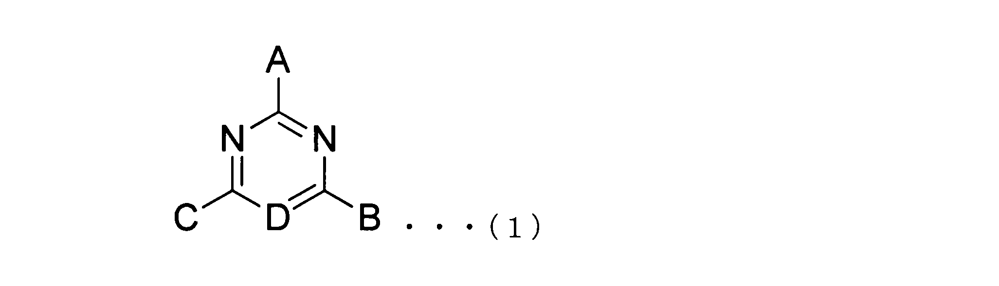
A、B、及びCは、それぞれ独立に、下記一般式(2-1)~(2-5)で表される置換基のうち、いずれかから選ばれる。
-Ar1-X1 ・・・(2-1)
-Ar2-Ar3-X2 ・・・(2-2)
-Ar4-Ar5-Ar6-X3 ・・・(2-3)
-Ar7-Ar8-Ar9-Ar10-X4 ・・・(2-4)
-Ar11-Ar12-Ar13-Ar14-Ar15-X5・・・(2-5)
上記一般式(2-1)~(2-5)において、Ar1は、置換基を有していてもよい1,2-フェニレン基または1,3-フェニレン基を表し、Ar2~Ar15は、それぞれ独立に、置換基を有していてもよい1,2-フェニレン基、1,3-フェニレン基または1,4-フェニレン基を表す。
X1は、置換基を有していてもよい炭素数10以上の芳香族炭化水素基、または置換基を有していてもよいカルバゾリル基を表し、X2~X5は、それぞれ独立に、置換基を有していてもよい芳香族炭化水素基、置換基を有していてもよいカルバゾリル基、置換基を有していてもよいジベンゾフラニル基、または置換基を有していてもよいジベンゾチオフェニル基を表す。
ただし、A、BおよびCは、いずれにおいても、1,2-フェニレン基及び1,3-フェニレン基のうち少なくとも1つを含み、A、B及びCは同時に同一の基を表すことはない。
Dは、CHまたは窒素原子を表す。]
[2] 前記一般式(2-2)~(2-5)において、Ar2~Ar15が表す置換基が、それぞれ独立に、1,3-フェニレン基または1,4-フェニレン基である、前記[1]に記載の有機化合物。
[3] 前記一般式(2-1)~(2-5)において、Ar1、Ar3、Ar6、Ar10、及びAr15が表す置換基が1,3-フェニレン基である、前記[1]または[2]に記載の有機化合物。
[4] 前記一般式(1)において、A、B及びCが互いに異なる置換基である、前記[1]~[3]のいずれか一に記載の有機化合物。
[5] 下記一般式(3)で表され、分子量750以上2000以下であって、分子中に存在するカルバゾリル基の数が1または0である有機化合物。

Dは、CHまたは窒素原子を表す。
E及びFは、それぞれ独立に、下記一般式(4-1)~(4-6)で表される置換基のうち、いずれかから選ばれる。
-X6 ・・・(4-1)
-Ar16-X7 ・・・(4-2)
-Ar17-ArX8 ・・・(4-3)
-Ar19-Ar-Ar21-X9 ・・・(4-4)
-Ar22-Ar23-Ar24-Ar25-X10 ・・・(4-5)
-Ar26-Ar27-Ar28-Ar29-Ar30-X11・・・(4-6)
上記一般式(4-1)~(4-6)において、Ar16は、置換基を有していてもよい1,2-フェニレン基または1,3-フェニレン基を表し、Ar17~Ar30は、それぞれ独立に、置換基を有していてもよい1,2-フェニレン基、1,3-フェニレン基または1,4-フェニレン基を表す。
X6~X11は、それぞれ独立に、置換基を有していてもよい芳香族炭化水素基、置換基を有していてもよいカルバゾリル基、置換基を有していてもよいジベンゾフラニル基、または置換基を有していてもよいジベンゾチエニル基を表す。
ただし、E、Fは、いずれにおいても、1,2-フェニレン基及び1,3-フェニレン基のうち少なくとも1つを含む。
Lは、直接結合、または、置換基を有していてもよい2価の芳香族炭化水素基を表し、R1~R5のいずれかの1つの置換位置との間で結合を形成する。
R1~R5は、それぞれ独立に、Lとの間での結合、水素原子、置換基を有していてもよいフェニル基、置換基を有していてもよいジベンゾフラニル基、置換基を有していてもよいジベンゾチエニル基、アルキル基、シリル基、フッ素原子、またはパーフルオロアルキル基を表し、R6~R18は、水素原子、置換基を有していてもよいフェニル基、置換基を有していてもよいジベンゾフラニル基、置換基を有していてもよいジベンゾチエニル基、アルキル基、シリル基、フッ素原子、またはパーフルオロアルキル基を表す。]
[6] 前記一般式(4-3)~(4-6)において、Ar17~Ar30が表す置換基が、それぞれ独立に、1,3-フェニレン基または1,4-フェニレン基である、前記[5]に記載の有機化合物。
[7] 前記一般式(4-2)~(4-6)において、Ar16、Ar18、Ar21、Ar25、及びAr30が表す置換基が1,3-フェニレン基である、前記[5]または[6]に記載の有機化合物。
[8] 前記[1]~[7]のいずれか一に記載の有機化合物を含有する電荷輸送材料。
[9] 前記[1]~[7]のいずれか一に記載の有機化合物及び溶剤を含有する組成物。
[10] 陽極、陰極、及び該陽極と陰極との間に少なくとも1層の有機層を有する有機電界発光素子であり、該有機層のうち少なくとも1層が、前記[9]に記載の組成物を用いて形成された層である、有機電界発光素子。
[11] 前記[9]に記載の組成物を用いて形成された層が発光層である、前記[10]に記載の有機電界発光素子。
[12] 前記[10]または[11]に記載の有機電界発光素子を有する表示装置。
[13] 前記[10]または[11]に記載の有機電界発光素子を有する照明装置。
ここで、“重量%”と“質量%”、“重量比”と“質量比”とは、それぞれ同義である。
本発明において、単に「芳香環」と称した場合には、芳香族炭化水素環及び芳香族複素環のいずれも含むものとする。
本発明において、「置換基を有していてもよい」とは、置換基を1又は2以上有していてもよいことを意味するものとする。
また、本発明において「環由来の基」とは、当該環から、水素原子を1つ除いて得られる一価の基、或いは、当該環から、水素原子を2つ除いて得られる二価の基を表す。例えば、置換基を有していてもよいベンゼン環由来の基とは、価数が1価の場合は置換基を有していてもよいフェニル基を表し、2価の場合は置換基を有していてもよいフェニレン基を表わす。また、特に断りがない限り結合位置に制限は無く、ベンゼン環由来の2価の基の場合は、1,2-フェニレン基、1,3-フェニレン基、1,4-フェニレン基を含む。
また、本発明において湿式成膜法とは、例えば、スピンコート法、ディップコート法、ダイコート法、バーコート法、ブレードコート法、ロールコート法、スプレーコート法、キャピラリーコート法、インクジェット法、スクリーン印刷法、グラビア印刷法、またはフレキソ印刷法等の、湿式で成膜される方法をいう。これらの成膜方法の中でも、スピンコート法、スプレーコート法、インクジェット法が好ましい。これは、有機電界発光素子に用いられる湿式成膜用の組成物特有の液性に合うためである。
本発明の有機化合物は、下記一般式(1)または(3)で表され、分子量が750以上2000以下であって、分子中のカルバゾリル基の数が1または0であることを特徴とする有機化合物(以下「本発明の有機化合物」と称す場合がある。)である。
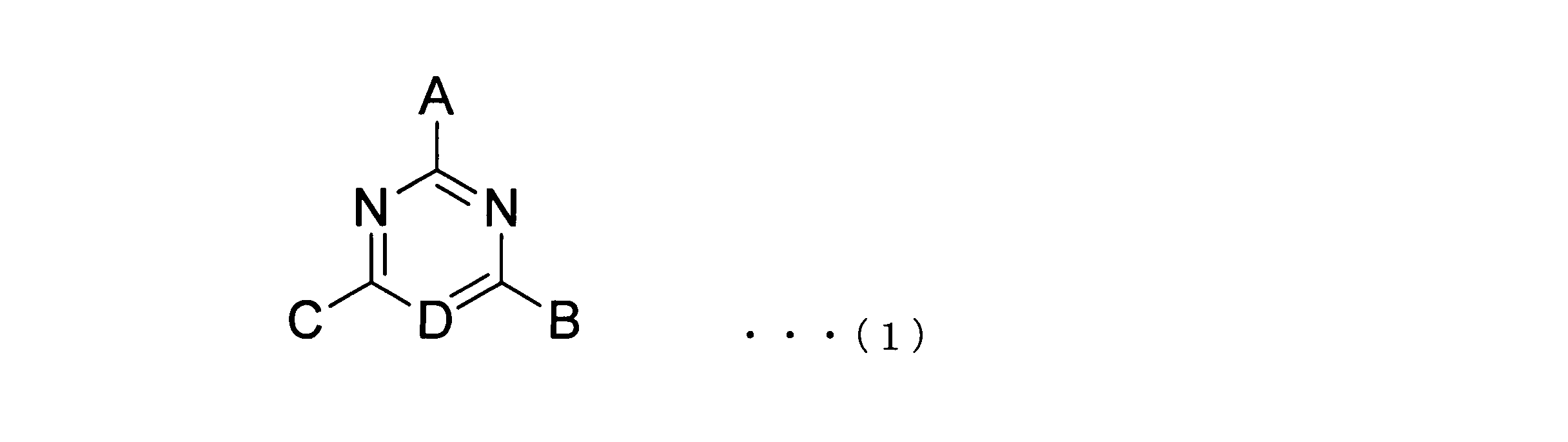
A、B、及びCは、それぞれ独立に、下記一般式(2-1)~(2-5)で表される置換基のうち、いずれかから選ばれる。
-Ar1-X1 ・・・(2-1)
-Ar2-Ar3-X2 ・・・(2-2)
-Ar4-Ar5-Ar6-X3 ・・・(2-3)
-Ar7-Ar8-Ar9-Ar10-X4 ・・・(2-4)
-Ar11-Ar12-Ar13-Ar14-Ar15-X5・・・(2-5)
上記一般式(2-1)~(2-5)において、Ar1は、置換基を有していてもよい1,2-フェニレン基または1,3-フェニレン基を表し、Ar2~Ar15は、それぞれ独立に、置換基を有していてもよい1,2-フェニレン基、1,3-フェニレン基または1,4-フェニレン基を表す。
X1は、置換基を有していてもよい炭素数10以上の芳香族炭化水素基、または置換基を有していてもよいカルバゾリル基を表し、X2~X5は、それぞれ独立に、置換基を有していてもよい芳香族炭化水素基、置換基を有していてもよいカルバゾリル基、置換基を有していてもよいジベンゾフラニル基、または置換基を有していてもよいジベンゾチオフェニル基を表す。
Dは、CHまたは窒素原子を表す。すなわちDがCHのとき、本発明の有機化合物はピリミジン環骨格を有する化合物であり、Dが窒素原子のとき、本発明の有機化合物は1,3,5-トリアジン環骨格を有する化合物である。
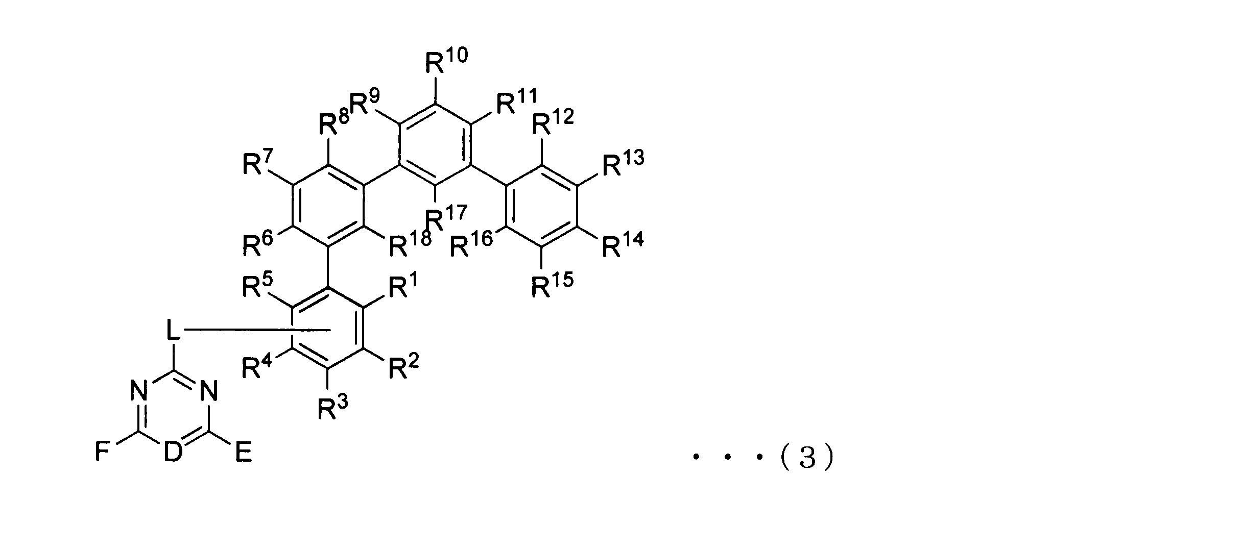
Dは、CHまたは窒素原子を表す。すなわちDがCHのとき、本発明の有機化合物はピリミジン環骨格を有する化合物であり、Dが窒素原子のとき、本発明の有機化合物は1,3,5-トリアジン環骨格を有する化合物である。
E、Fは、それぞれ独立に、下記一般式(4-1)~(4-6)で表される置換基のうち、いずれかから選ばれる。
-X6 ・・・(4-1)
-Ar16-X7 ・・・(4-2)
-Ar17-Ar18-X8 ・・・(4-3)
-Ar19-Ar20-Ar21-X9 ・・・(4-4)
-Ar22-Ar23-Ar24-Ar25-X10 ・・・(4-5)
-Ar26-Ar27-Ar28-Ar29-Ar30-X11・・・(4-6)
X6~X11は、それぞれ独立に、置換基を有していてもよい芳香族炭化水素基、置換基を有していてもよいカルバゾリル基、置換基を有していてもよいジベンゾフラニル基、または置換基を有していてもよいジベンゾチエニル基を表す。
ただし、E、Fは、いずれにおいても、1,2-フェニレン基及び1,3-フェニレン基のうち少なくとも1つを含む。
R1~R5は、それぞれ独立に、水素原子、置換基を有していてもよいフェニル基、置換基を有していてもよいジベンゾフラニル基、置換基を有していてもよいジベンゾチエニル基、アルキル基、シリル基、フッ素原子、またはパーフルオロアルキル基を表し、R6~R18は、水素原子、置換基を有していてもよいフェニル基、置換基を有していてもよいジベンゾフラニル基、置換基を有していてもよいジベンゾチエニル基、アルキル基、シリル基、フッ素原子、またはパーフルオロアルキル基を表す。
Lは、直接結合、または、置換基を有していてもよい2価の芳香族炭化水素基を表し、R1~R5のいずれかの1つの置換位置との間で結合を形成する。
前記一般式(2-1)および(4-2)において、Ar1ならびにAr16は置換基を有していてもよい1,2-フェニレン基、または置換基を有していてもよい1,3-フェニレン基であるが、耐久性の観点から、置換基を有していてもよい1,3-フェニレン基であることが特に好ましい。
前記一般式(2-1)において、X1を構成する炭素数10以上の芳香族炭化水素基としては、炭素数10~30の芳香族炭化水素基が好ましく、特に、6員環の2~5縮合環由来の基が好ましい。
X1の芳香族炭化水素基としては、具体的には、ナフタレン環、アントラセン環、フェナントレン環、ペリレン環、テトラセン環、ピレン環、ベンズピレン環、クリセン環、トリフェニレン環、フルオランテン環由来の基等が挙げられる。中でも、三重項励起準位が比較的低く、有機溶剤に対する溶解性が比較的高いという点から、ナフタレン環、フェナントレン環由来の基が好ましい。
X1の芳香族炭化水素基のAr1との結合位置については、特に限定はされないが、化学的安定性や電荷輸送性の観点から、例えばナフチル基であればナフタレン環の1位、フェナンチル基であればフェナントレン環の9位、10位において結合していることが好ましい。
X2~X5、及びX7~X11を構成する各芳香族炭化水素基のAr3、Ar6、Ar10、Ar15、Ar16、Ar18、Ar21、Ar25、Ar30との結合位置、ならびにX6を構成する芳香族炭化水素基の1,3,5-トリアジン環もしくはピリミジン環との結合位置については、特に限定はされないが、化学的安定性や電荷輸送性の観点から、例えばナフチル基であればナフタレン環の1位、フェナンチル基であればフェナントレン環の9位、または10位において結合していることが好ましい。
前記一般式(3)の置換基Lは、直接結合、または、置換基を有していてもよい2価の芳香族炭化水素基(置換基を有していてもよい2価のアリーレン基)を表し、一方は、1,3,5-トリアジン環もしくはピリミジン環と結合し、もう一方は、R1~R5のいずれかの置換位置で、R1~R5のいずれかの代わりにベンゼン環と結合する。中でも、溶解性、耐久性の観点から、R2~R4のいずれかの置換位置で結合を形成する方が特に好ましい。Lの2価の芳香族炭化水素基としては、具体的には、1,2-フェニレン基、1,3-フェニレン基、1,4-フェニレン基、4,4’-ビフェニリレン、4,3’-ビフェニリレン、3,4’-ビフェニリレン、3,3’-ビフェニリレン等が挙げられる。中でも、有機溶剤に対する溶解性が比較的高いという点から、1,3-フェニレン基、3,3’-ビフェニリレン基が好ましい。
前記一般式(3)の置換基R1~R5は、それぞれ独立に、Lとの間での結合、置換基を有していてもよいフェニル基、置換基を有していてもよいジベンゾフラニル基、置換基を有していてもよいジベンゾチエニル基、アルキル基、シリル基、フッ素原子、またはパーフルオロアルキル基を表す。R6~R18は、それぞれ独立に、水素原子、置換基を有していてもよいフェニル基、置換基を有していてもよいジベンゾフラニル基、置換基を有していてもよいジベンゾチエニル基、アルキル基、シリル基、フッ素原子、またはパーフルオロアルキル基を表す(このうち、フェニル基、ジベンゾフラニル基、ジベンゾチエニル基については、さらにアルキル基、シリル基、フッ素原子、パーフルオロアルキル基を有していてもよい)。なお、ジベンゾフラニル基、ジベンゾチエニル基と各芳香環との結合位置については前述と同様である。
アルキル基としては、炭素数1~20のアルキル基が好ましく、具体的には、メチル基、エチル基、プロピル基、iso-プロピル基、ブチル基、iso-ブチル基、sec-ブチル基、tert-ブチル基、ペンチル基、ヘキシル基、オクチル基、シクロヘキシル基、デシル基、オクタデシル基等が挙げられる。中でも、耐久性の面から、メチル基、エチル基、tert-ブチル基といった炭素数4以下のものがより好ましい。
シリル基としては、炭素数1~4のアルキル基、または、炭素数6~20のアリール基が結合しているものが好ましく、具体的には、トリイソプロピルシリル基、トリフェニルシリル基、ジメチルフェニルシリル基、tert-ブチルジフェニルシリル基などが挙げられる。中でも、耐久性の面から、トリフェニルシリル基が好ましい。
パーフルオロアルキル基とは、アルキル基を構成する水素原子のすべてがフッ素原子に置換された置換基のことを指す。この置換基としては、炭素数1~4のパーフルオロアルキル基が好ましく、具体的には、トリフルオロメチル基、ペンタフルオロエチル基等が挙げられ、中でも耐久性の面から、トリフルオロメチル基がより好ましい。
前記一般式(2-1)~(2-5)および前記一般式(4-1)~(4-6)において、Ar1~Ar30、ならびに、X1~X11のそれぞれが有していてもよい置換基としては、フェニル基、ジベンゾフラニル基、ジベンゾチエニル基、アルキル基、シリル基、フッ素原子、パーフルオロアルキル基等が挙げられる(このうち、フェニル基、ジベンゾフラニル基、ジベンゾチエニル基については、さらにアルキル基、シリル基、フッ素原子、パーフルオロアルキル基を有していてもよい)。中でも耐久性の面から、フェニル基、アルキル基、またはシリル基であることが好ましい。なお、ジベンゾフラニル基、ジベンゾチエニル基とAr1~Ar30、ならびに、X1~X11との結合位置については前述と同様であり、アルキル基、シリル基、パーフルオロアルキル基については<R1~R18>の項で述べたものと同様である。
前記一般式(1)の置換基A、B、Cはそれぞれ、少なくとも1つの、置換基を有していてもよい1,2-フェニレン基または置換基を有していてもよい1,3-フェニレン基を含むものであり、また、置換基A、B、Cがすべて同一であることはないものである。さらに、分子の対称性を低下させて、有機溶剤に対する溶解性の向上ならびに材料の非晶質性の向上を図るために、前記一般式(1)における置換基A、B、Cは、互いに異なること、即ち、いずれもが同一でない置換基であることがより好ましい。ここで、「同一でない」とは、置換基A、B、Cを構成する芳香環の種類、芳香環が有する置換基、芳香環の他の基との結合順および結合位置のうち、少なくとも一つが異なることを指す。
本発明の有機化合物はカルバゾリル基を1個のみ有するか、或いはカルバゾリル基を有さないことが好ましい。
本発明の有機化合物の分子量は、通常2000以下、好ましくは1500以下、より好ましくは1300以下であり、また通常750以上、好ましくは800以上である。分子量が上記上限値を超えると、合成工程で生じる不純物成分の増加に伴って、材料の高純度化(すなわち劣化原因物質の除去)が困難になる場合があり、また、分子量が上記下限値を下回ると、溶解性、ガラス転移点温度、融点、気化温度、成膜性、および、膜質などが著しく低下するため、有機電界発光素子の耐熱性が著しく損なわれる恐れがある。
本発明の有機化合物の有機溶剤に対する溶解度を大きくし、該化合物と有機溶剤とを含有する組成物の保存安定性を確保しつつ、該組成物を用いて形成される有機電界発光素子の熱的耐久性を確保するため、本発明の有機化合物のガラス転移点温度(以下、「Tg」と称する場合がある)としては、70℃以上125℃以下が好ましく、より好ましくは75℃以上125℃以下である。
装置:エスアイアイ・ナノテクノロジー株式会社 DSC6220
試料量:約4mg
試料容器:Al製液体用試料容器
雰囲気:N2,50ml/min
温度範囲:室温~300℃
昇温速度:10℃/min
以下に、本発明の有機化合物の好ましい具体例を示すが、本発明の有機化合物は、以下の例示化合物に限定されるものではない。
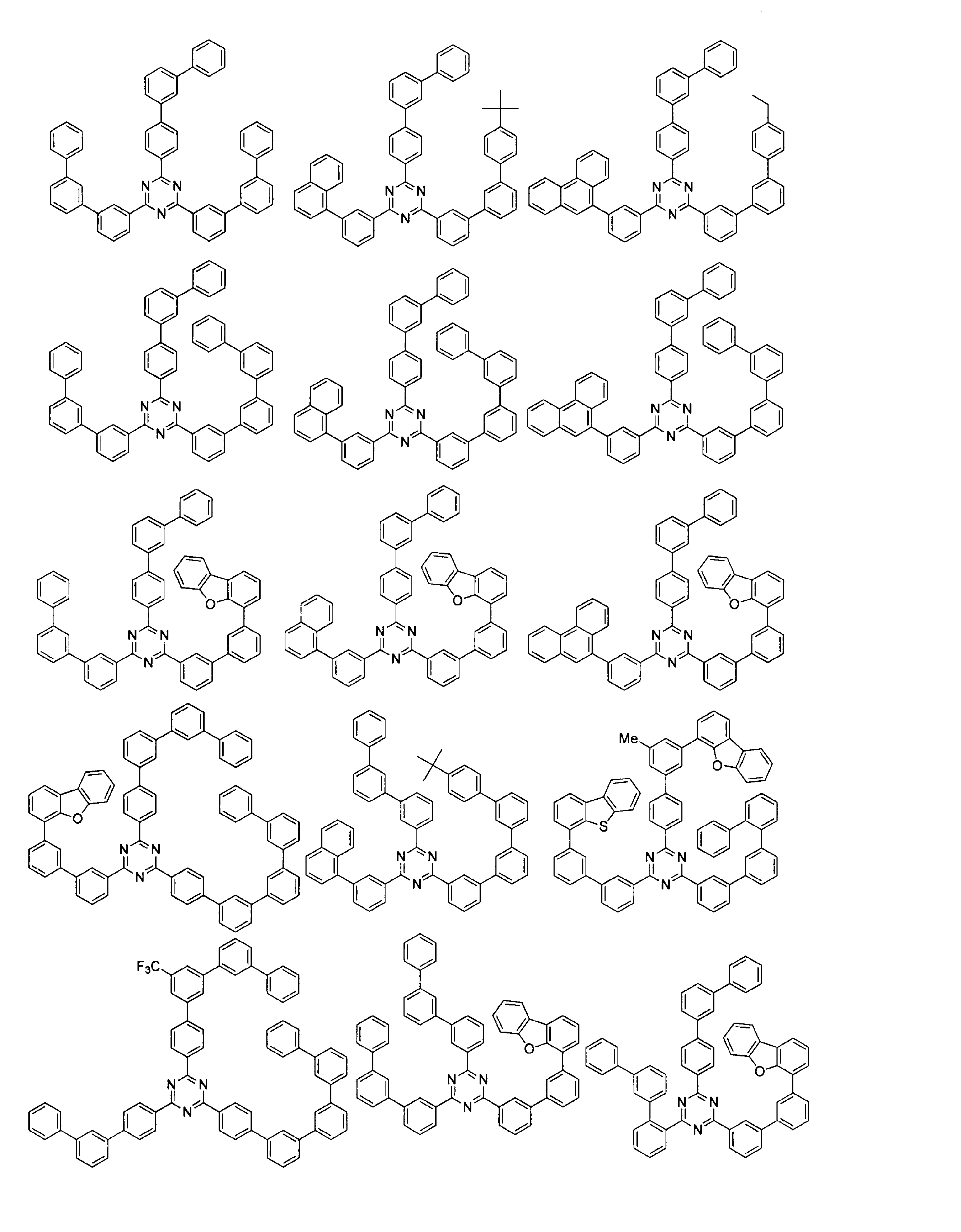
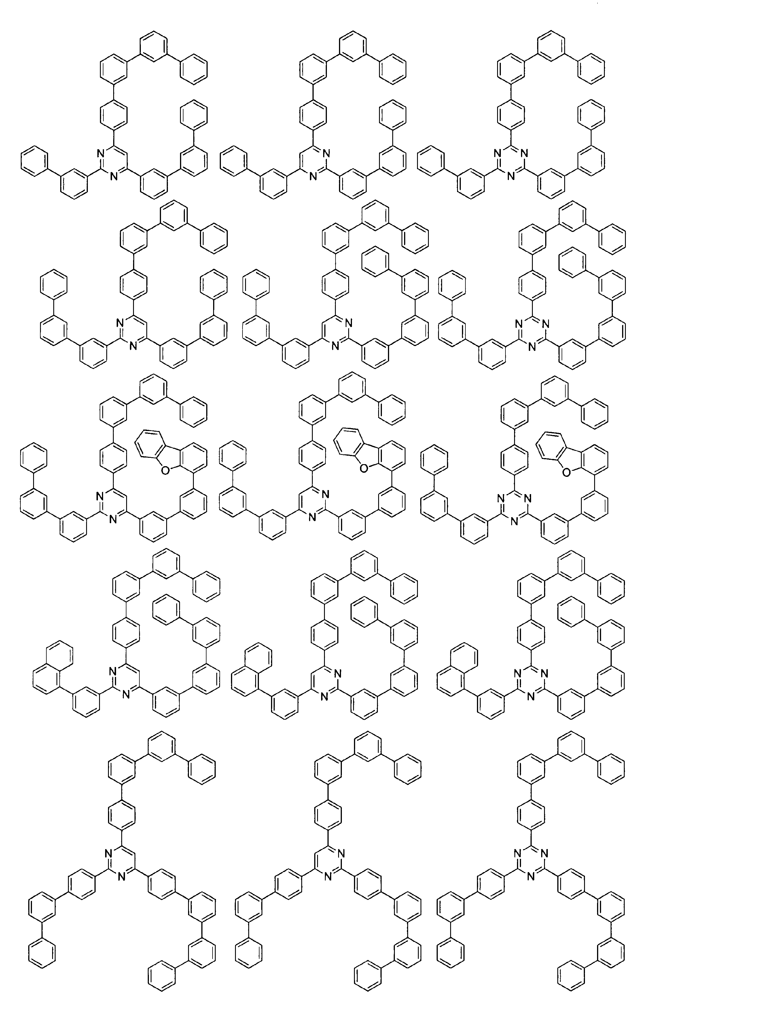
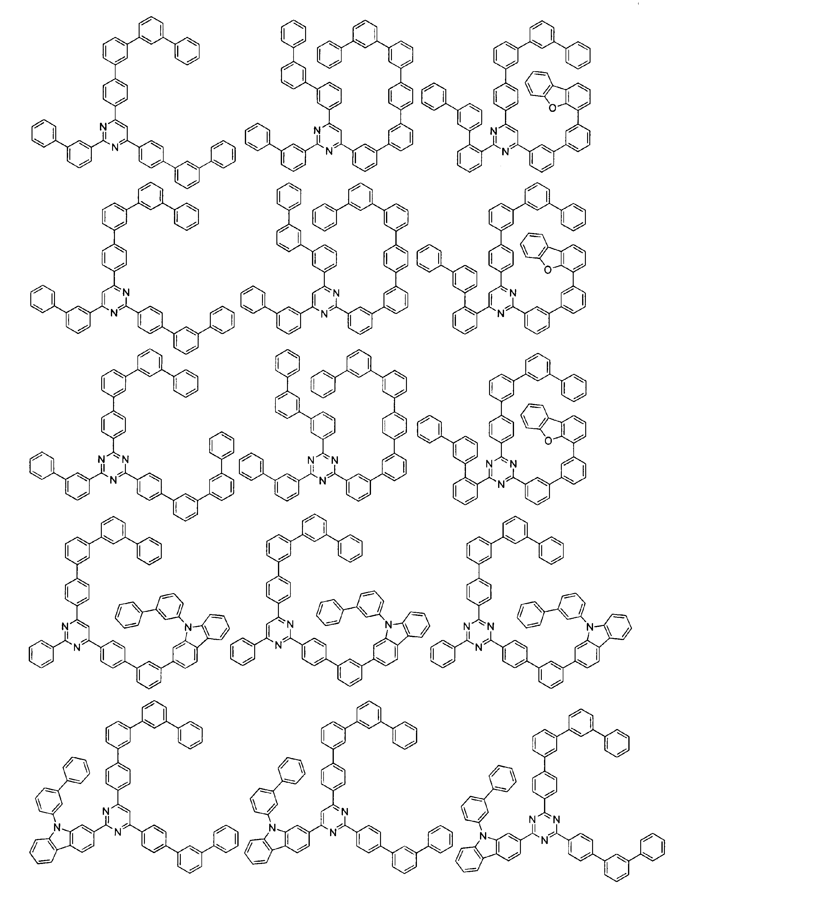
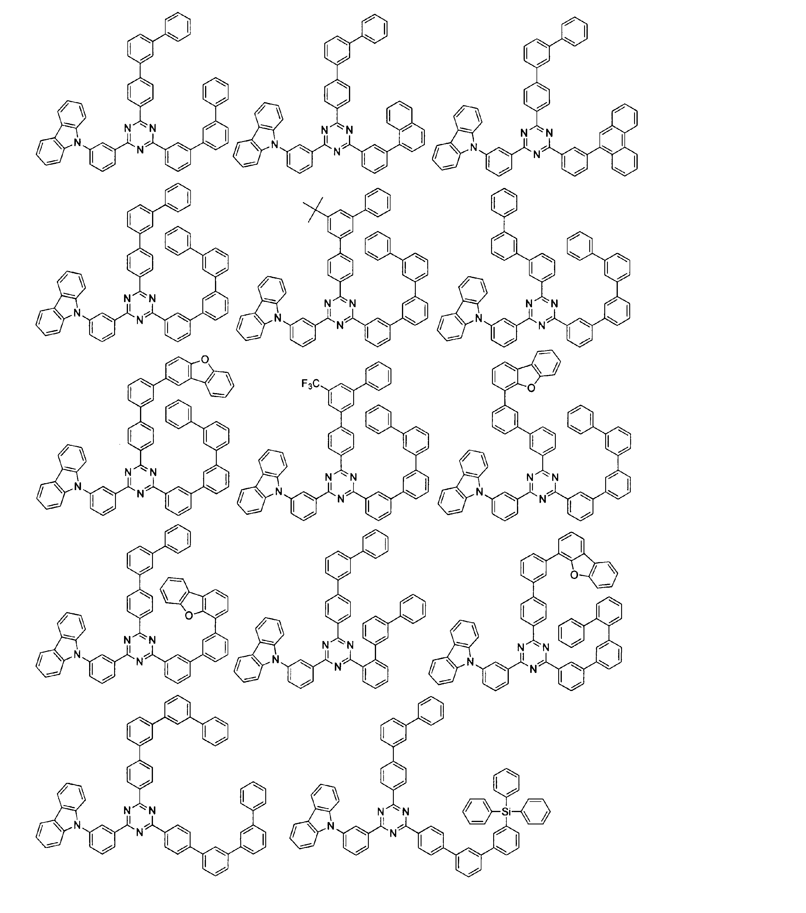
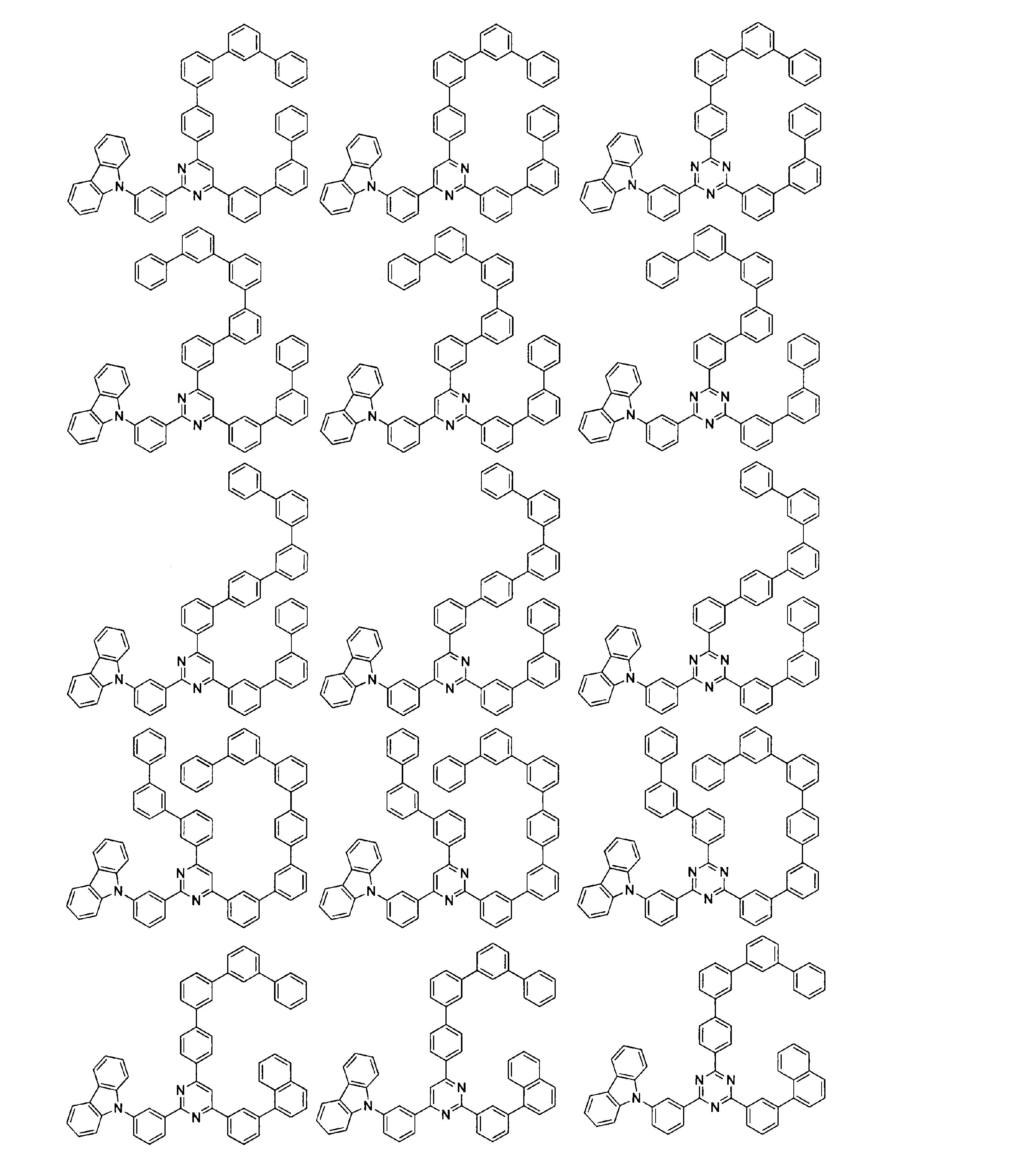
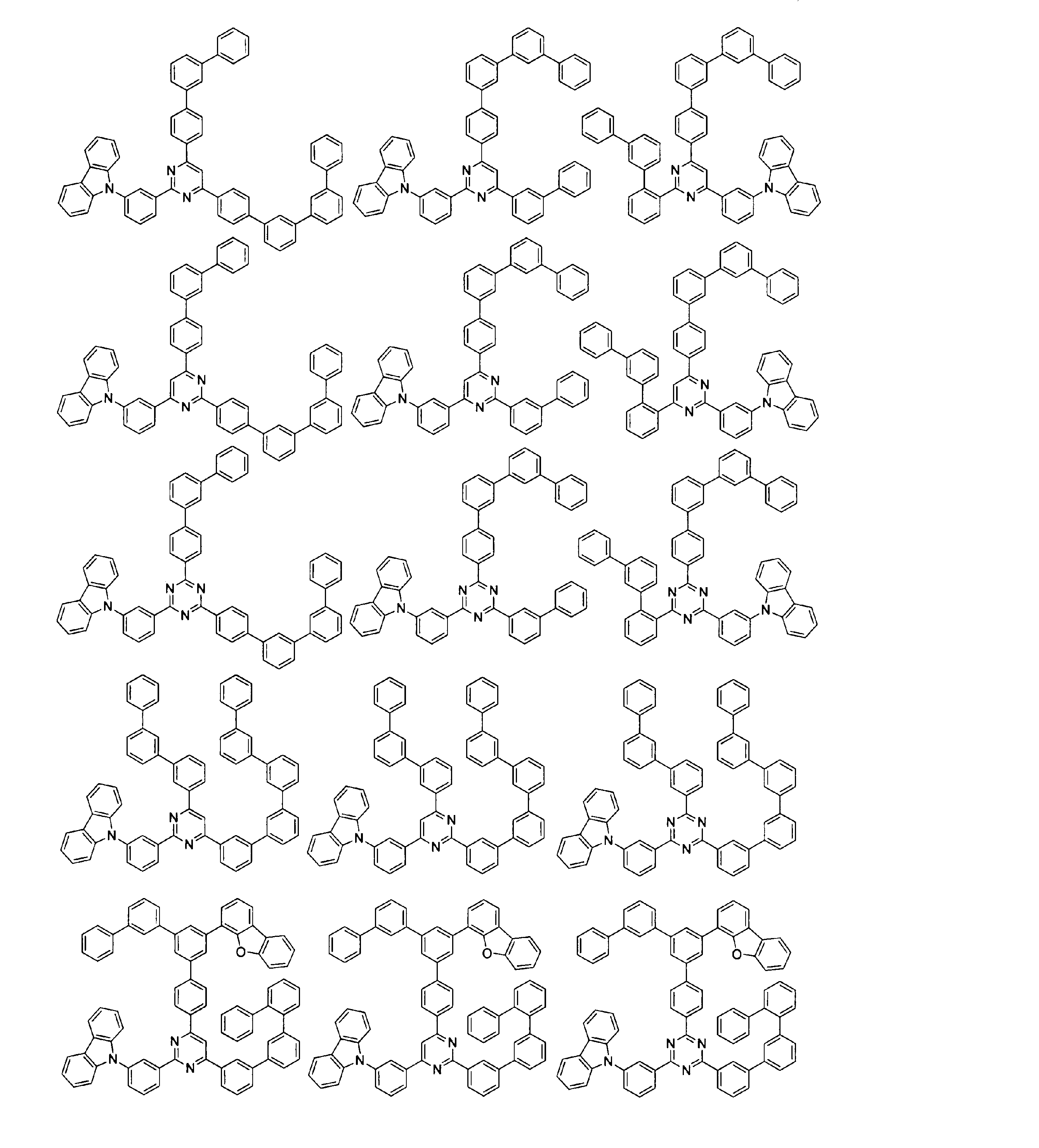
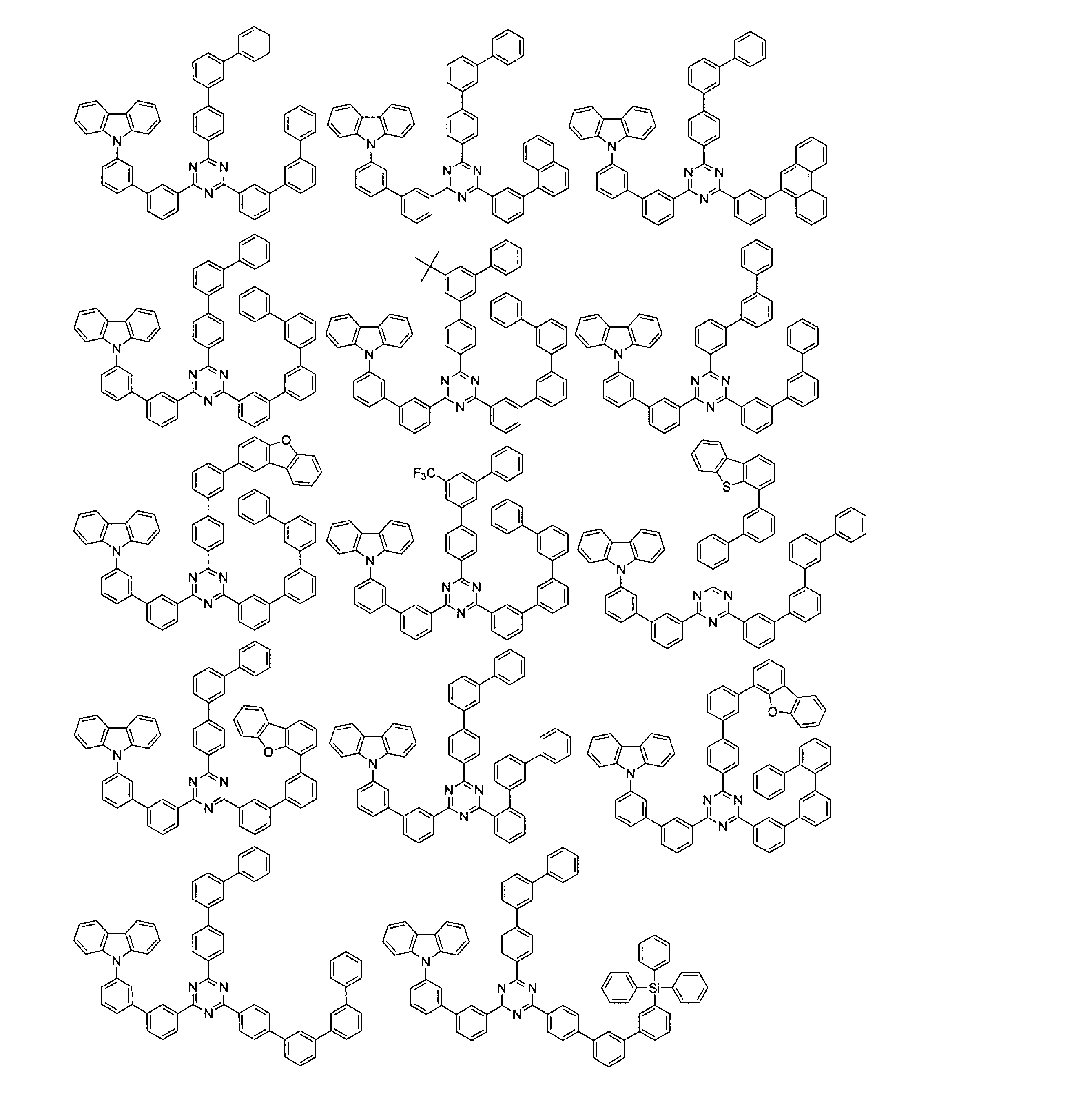
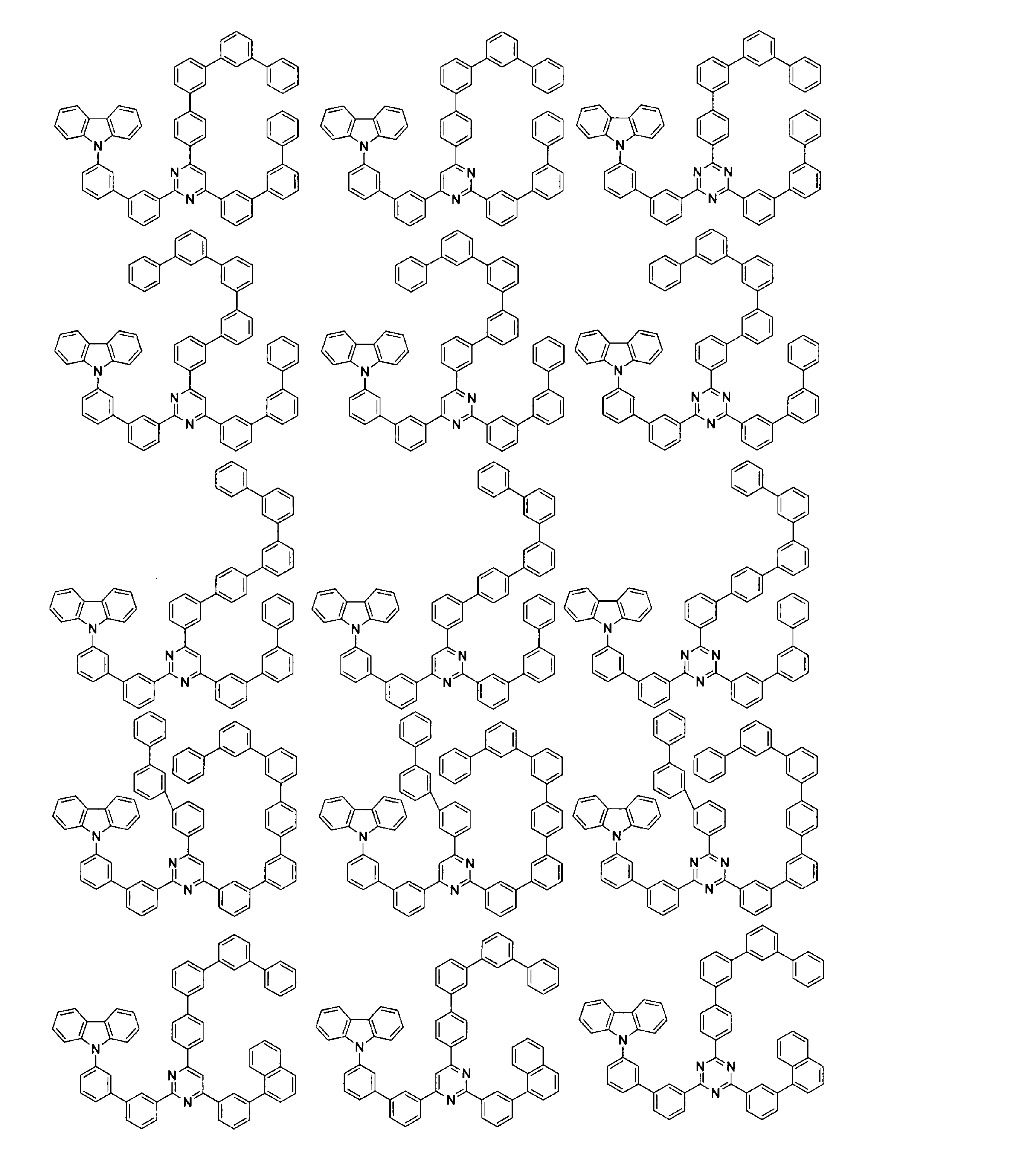

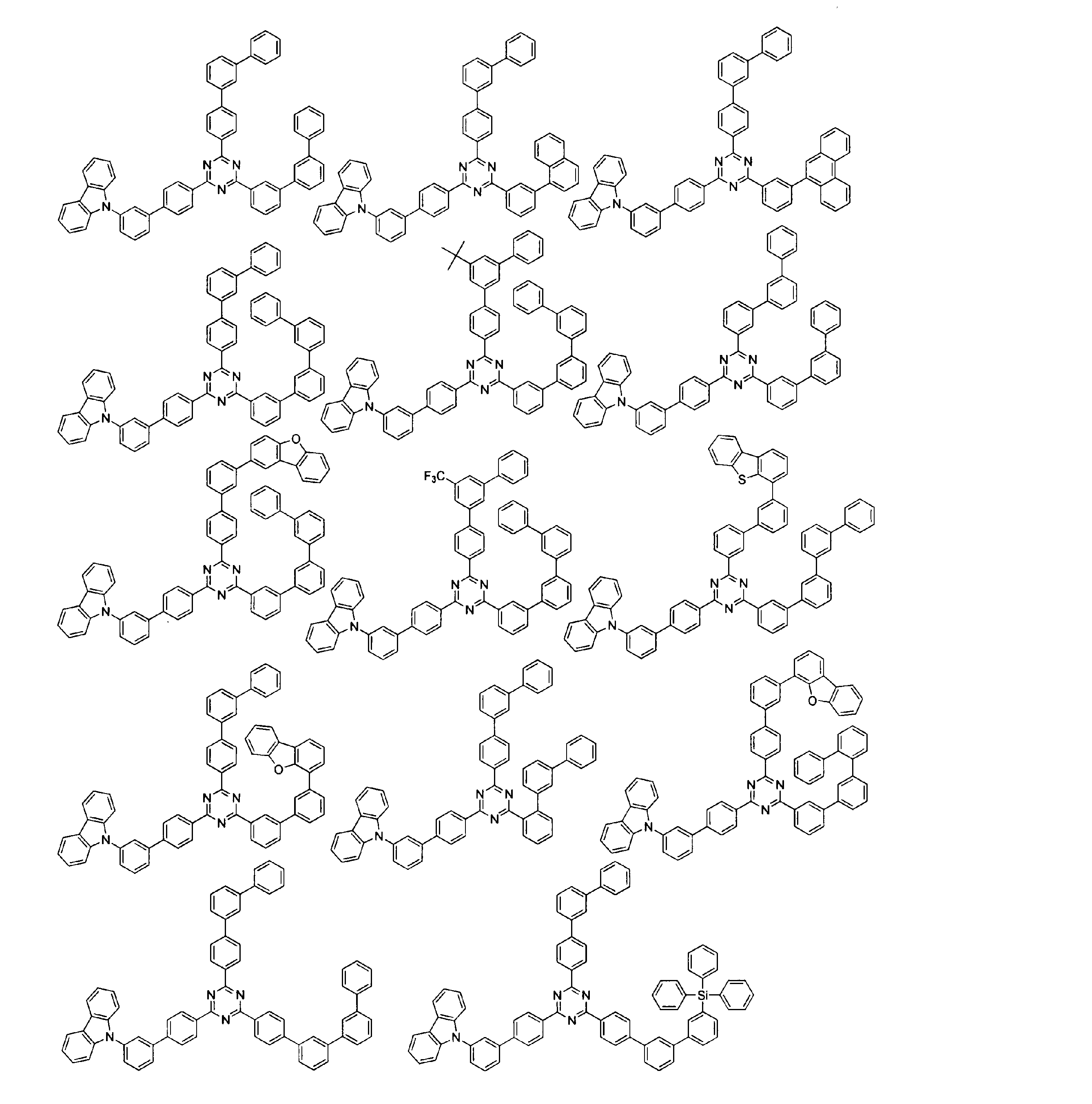
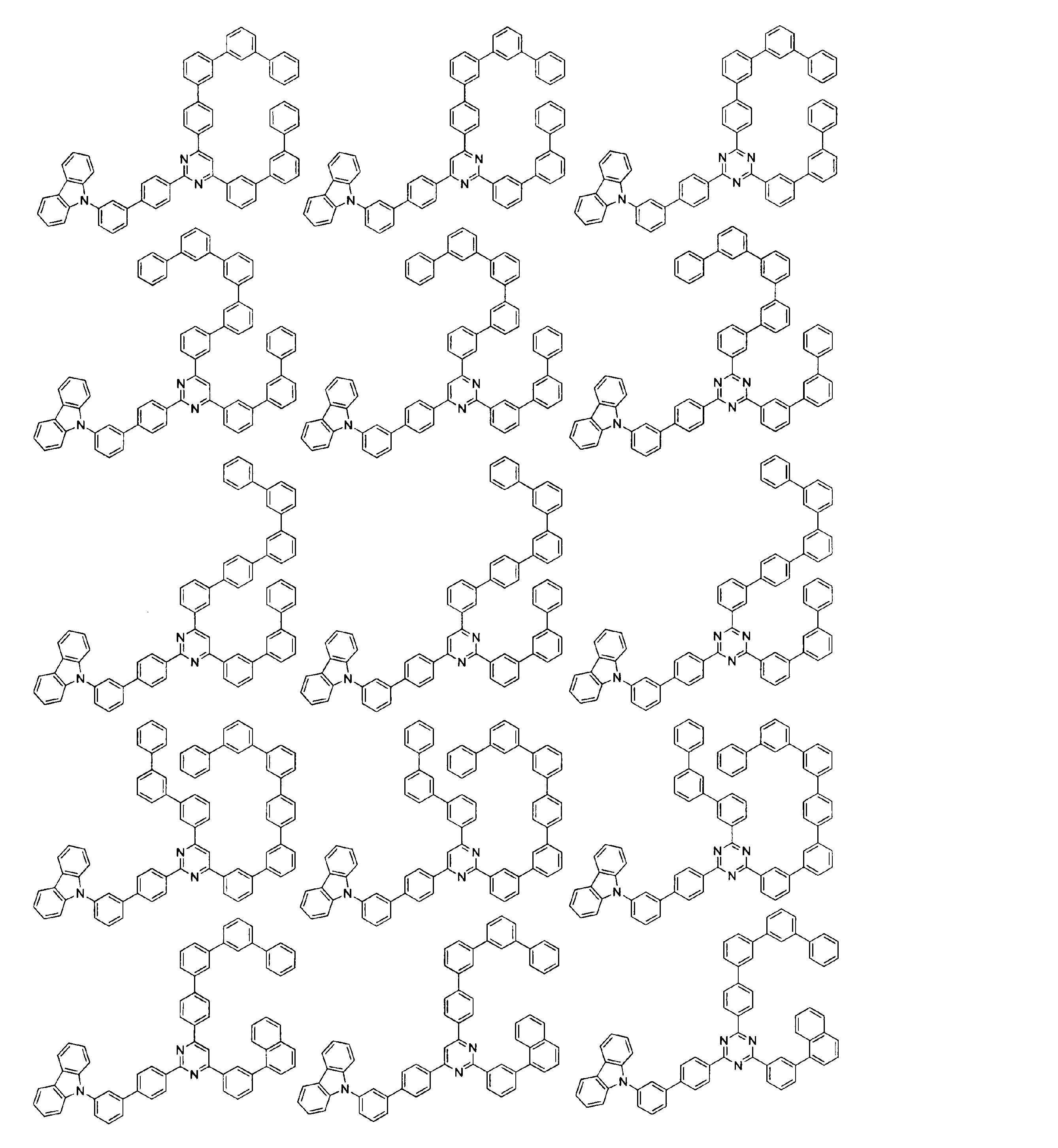
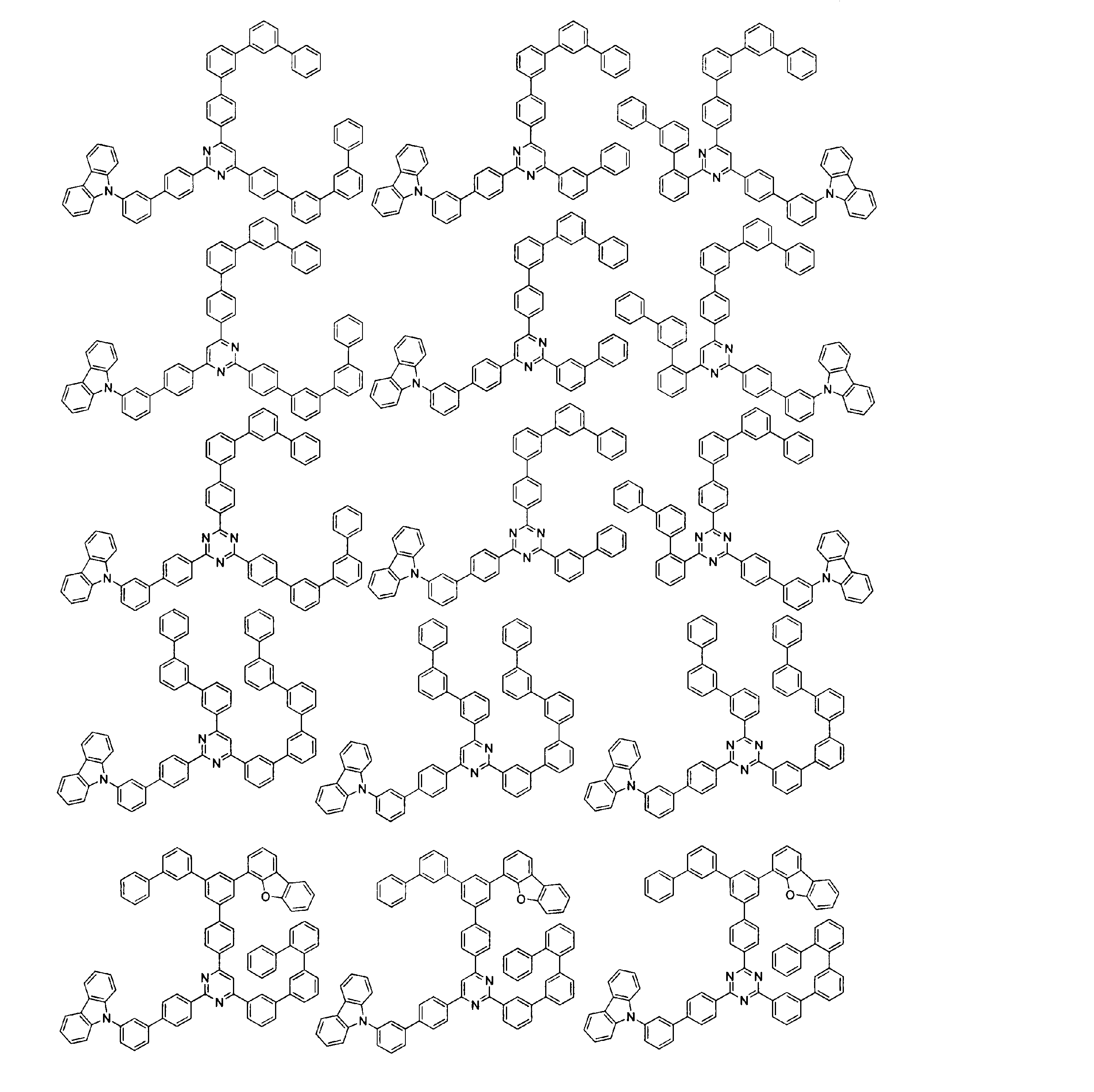
前記一般式(1)で表される本発明の有機化合物は、例えば下記に示す公知の方法を適宜組み合わせることで合成することができる。
参考文献:Advanced Materials,2010年,22巻,3311-3316頁
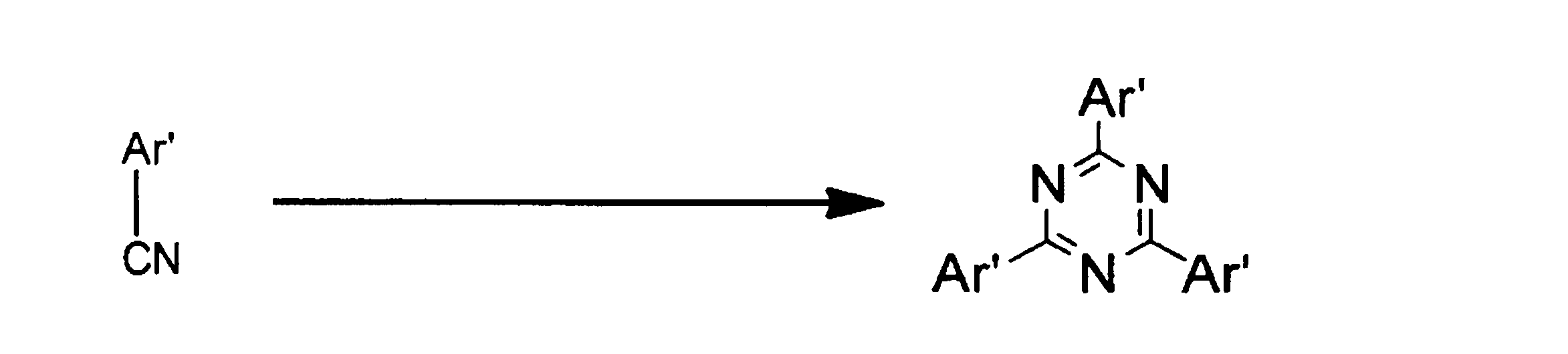
参考文献:Journal of Organic Chemistry,2002年、67巻、24号、8424-8429頁;Synthetic Metals、2001年、122巻、3号、485-493頁;Organic Letters,2001年、3巻、15号、2419-2421頁;Organic Letters,2008年、10巻、5号、709-712頁;Chemistry of Materials、2006年、18巻、204-213頁
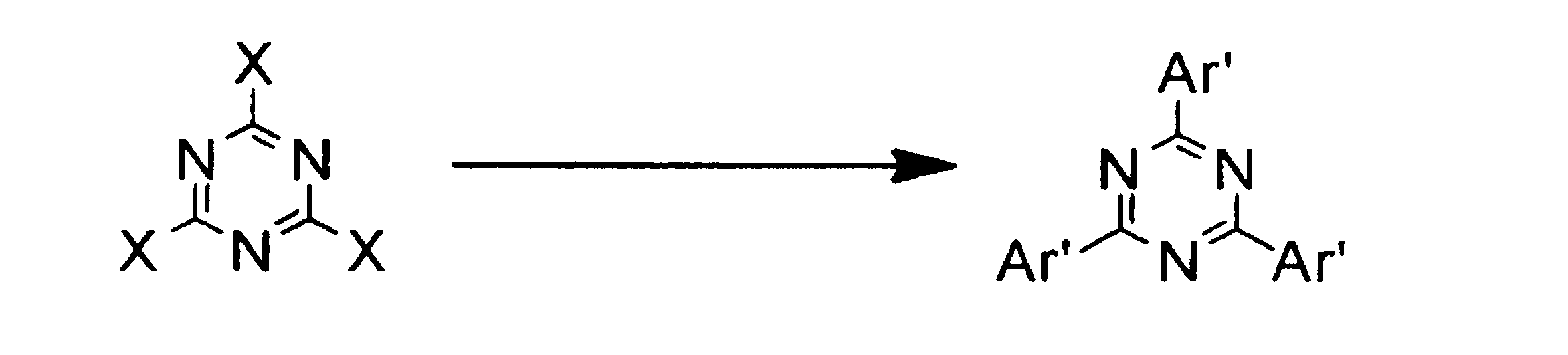

本発明の有機化合物の化学構造とすることで本発明の目的とする効果が奏されるメカニズムの詳細については明らかではないが、以下の通り推測される。

本発明の有機化合物は、発光材料、電荷輸送材料(電荷輸送性化合物)として用いられることが好ましく、また、有機電界発光素子における発光層の発光材料、電荷輸送材料として用いることが好ましく、特に電荷輸送材料として用いられることが好ましい。
本発明の組成物は、本発明の有機化合物と溶剤とを含有する。なお、前記本発明の有機化合物は、本発明の組成物中に、1種のみ含まれていてもよく、2種以上が組み合わされて含まれていてもよい。また、本発明の組成物が電荷輸送材料として本発明の有機化合物を含む場合であっても、さらに従来電荷輸送材料として用いられている他の化合物を含有することができる。
本発明の組成物に含有され得る溶剤は、好ましくは、湿式成膜法により有機層を形成するために用いる、揮発性を有する液体成分である。
本発明の組成物は、さらに発光材料を含有することが好ましい。
(式(II)中、Mは金属原子を表し、qは上記金属原子の価数を表す。また、L及びL’は二座配位子を表す。jは0、1又は2を表す。)

式(II)中、Mは任意の金属原子を表し、好ましいものの具体例としては、周期表第7ないし11族から選ばれる金属原子として前述した金属原子が挙げられる。
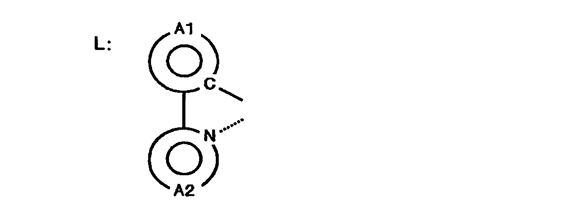
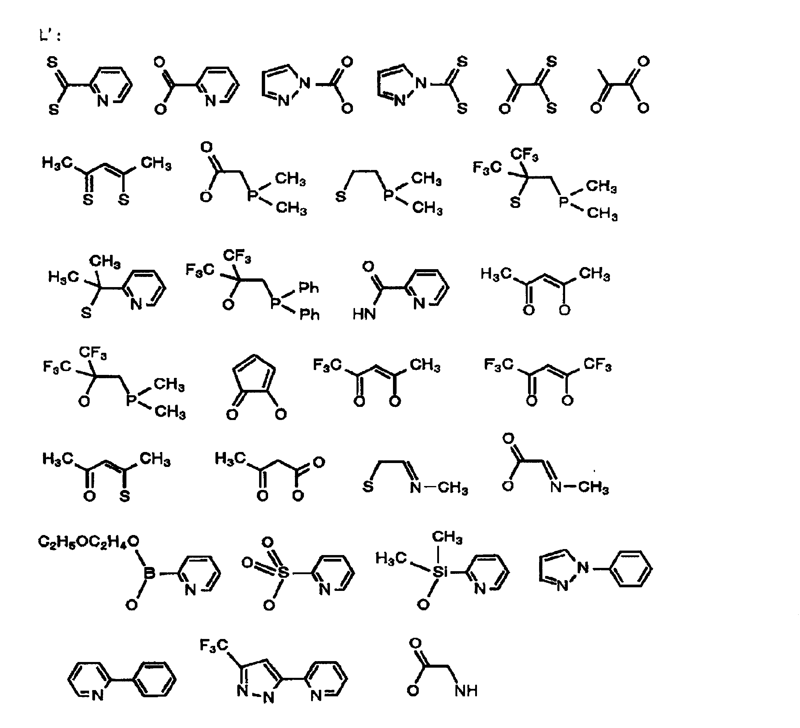
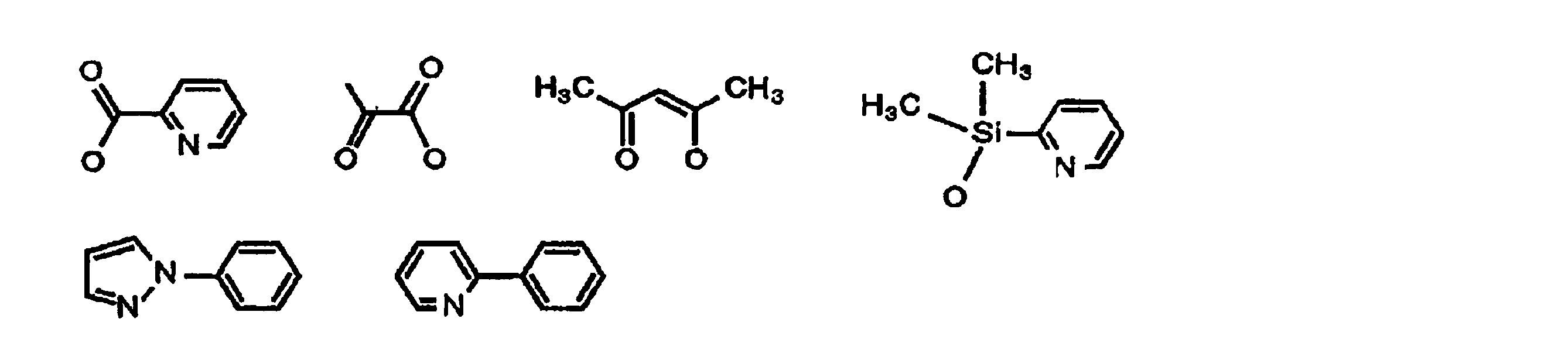
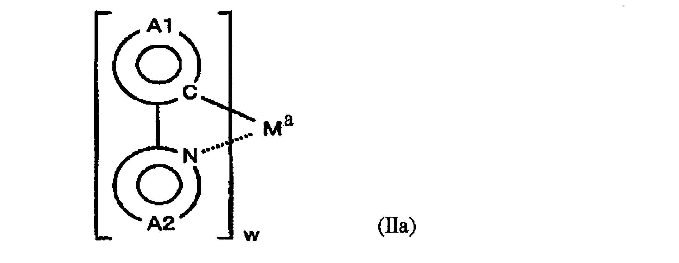

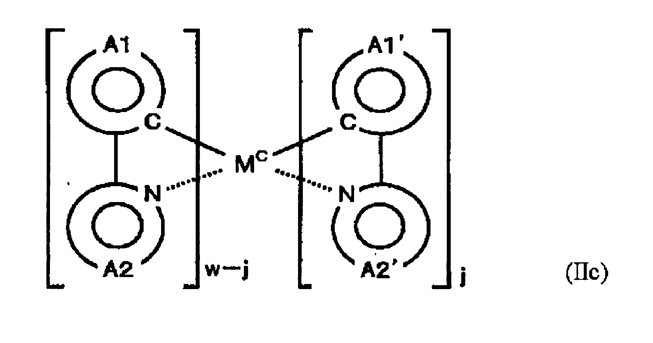
なお、これら置換基は互いに連結して環を形成してもよい。具体例としては、環A1が有する置換基と環A2が有する置換基とが結合するか、又は、環A1’が有する置換基と環A2’が有する置換基とが結合するかして、一つの縮合環を形成してもよい。このような縮合環基としては、7,8-ベンゾキノリン基等が挙げられる。

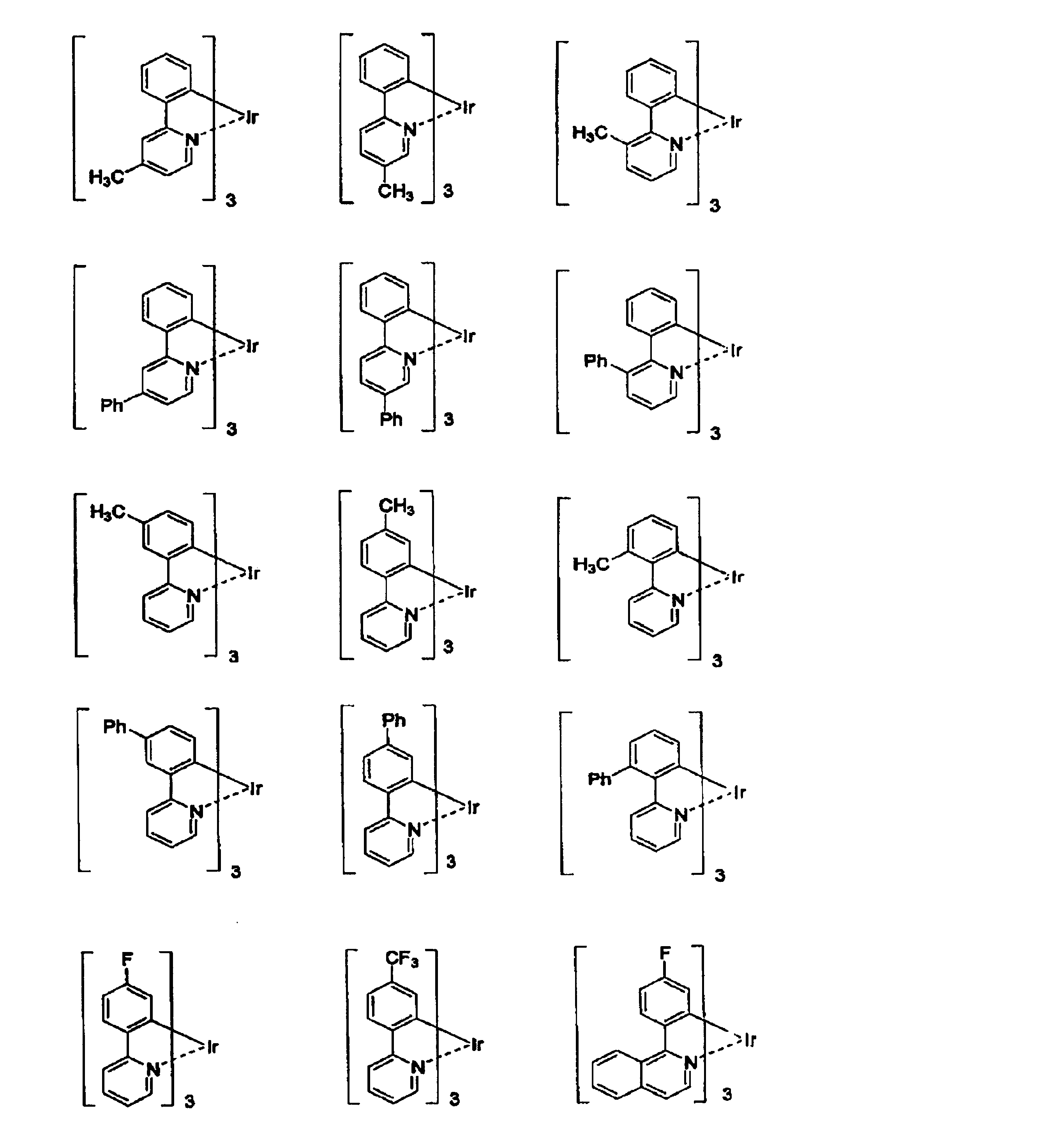
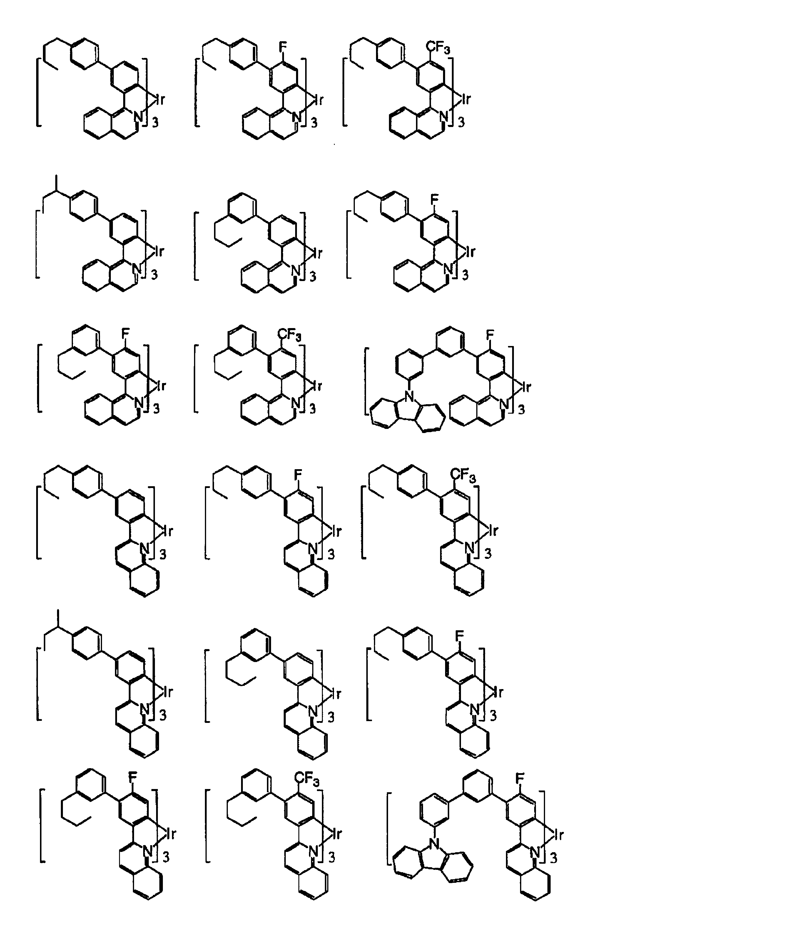
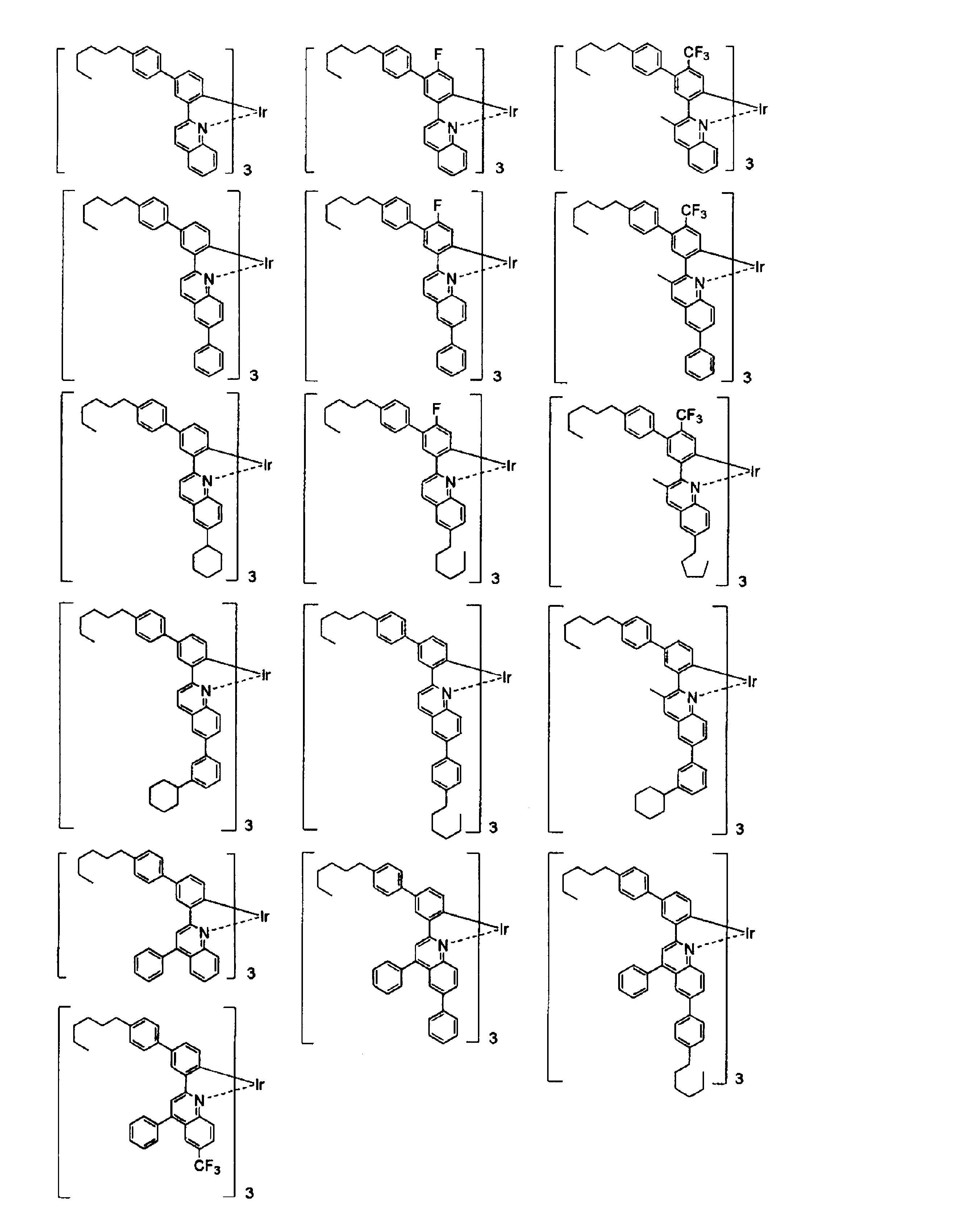
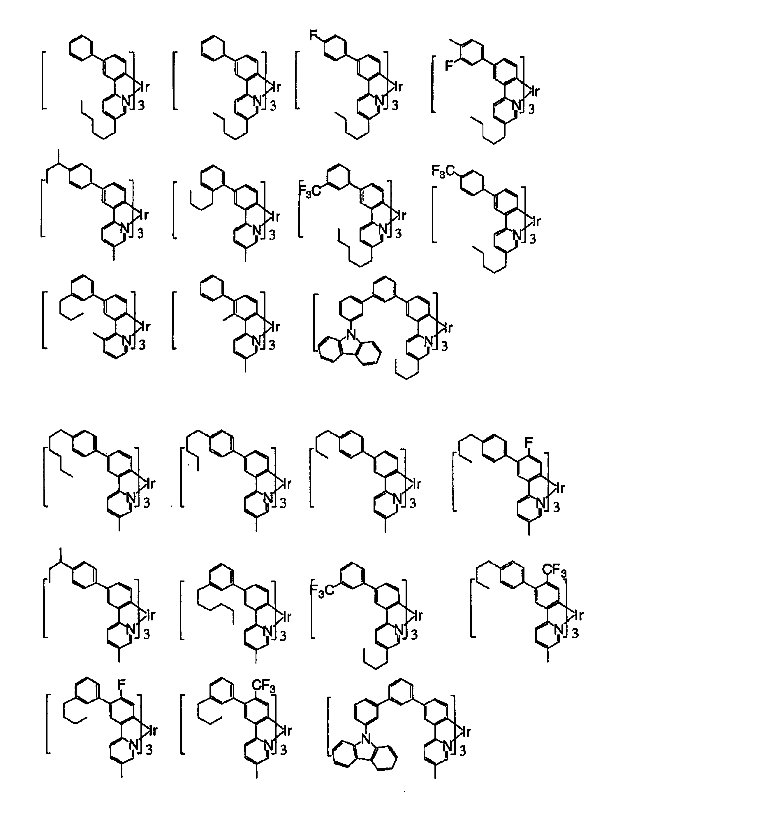
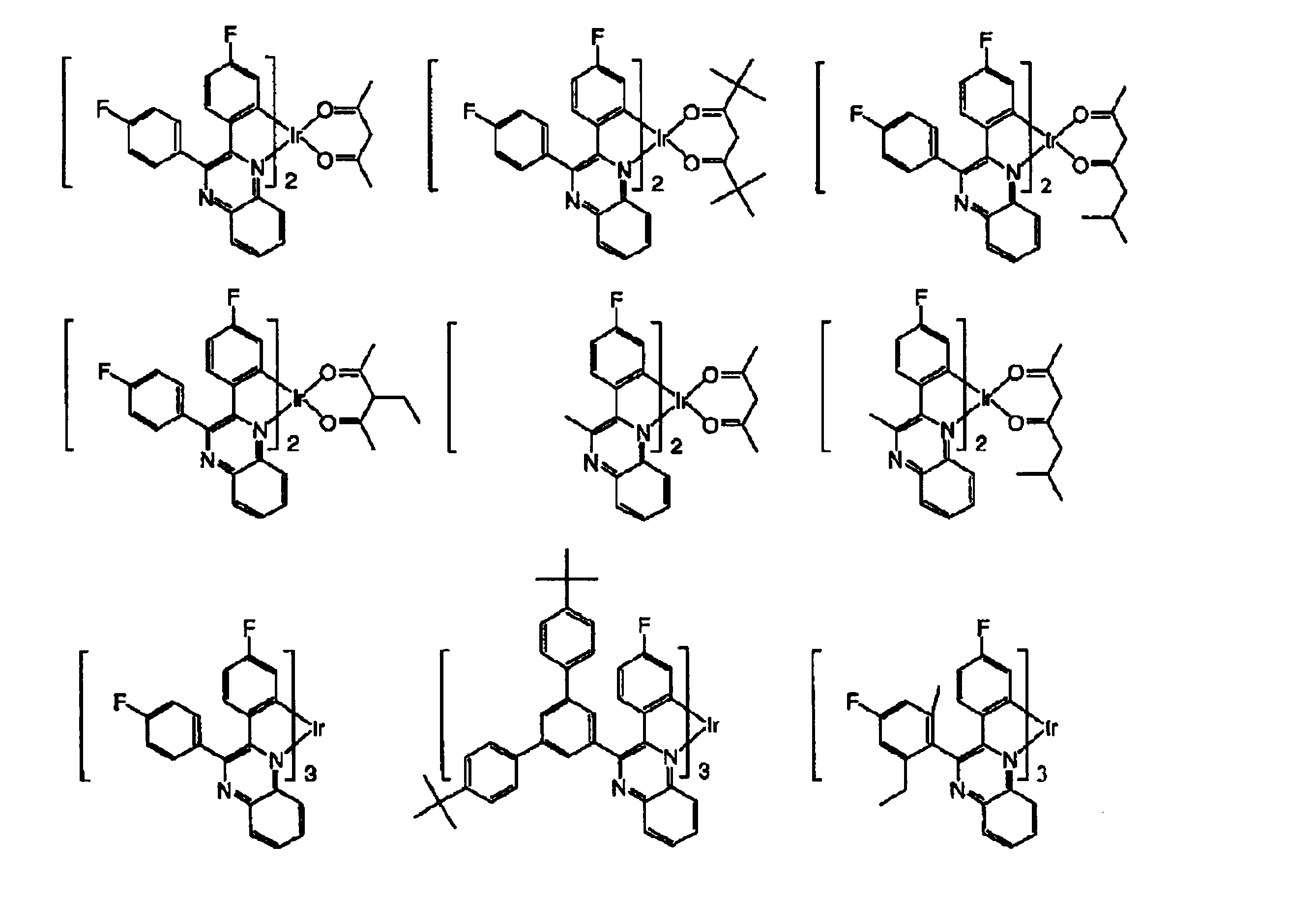
式(III)中、Mdは金属原子を表し、具体例としては、周期表第7ないし11族から選ばれる金属原子として前述した金属原子が挙げられる。中でも好ましくは、ルテニウム、ロジウム、パラジウム、銀、レニウム、オスミウム、イリジウム、白金又は金が挙げられ、特に好ましくは、白金、パラジウム等の2価の金属原子が挙げられる。
さらに、R92~R95は互いに連結して環を形成してもよく、この環がさらに任意の置換基を有していてもよい。
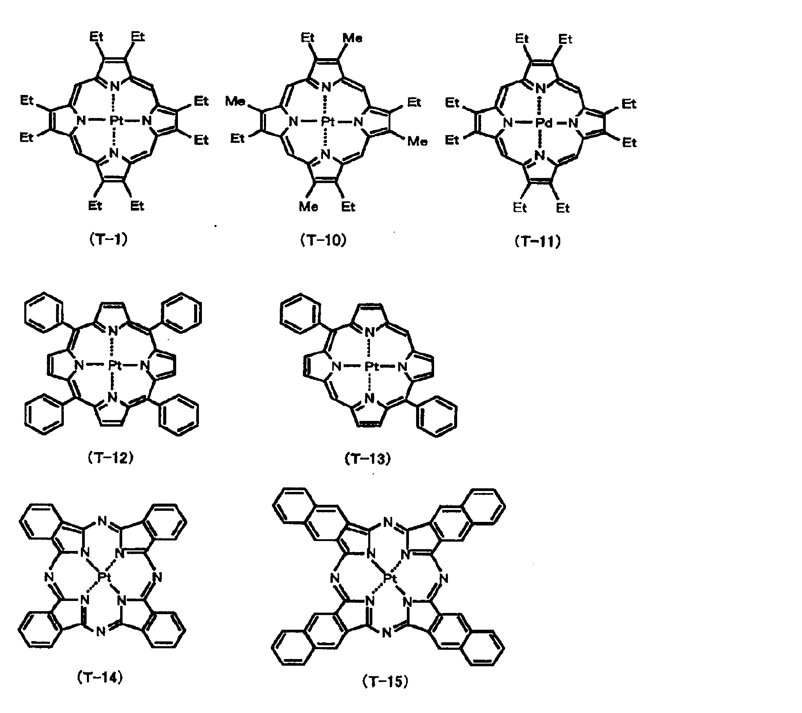
本発明の組成物は、本発明の有機化合物を電荷輸送材料として含むことが好ましいが、さらにその他の電荷輸送材料を含んでいてもよい。以下に、併用できる電荷輸送材料の好ましい具体例を示すが、本発明はこれらに限定されるものではない。
正孔輸送材料としては、例えば、トリアリールアミンやカルバゾールを部分構造として有する化合物が挙げられる。以下に、正孔輸送材料の具体例を以下に示すがこれらに限定されるものではない。
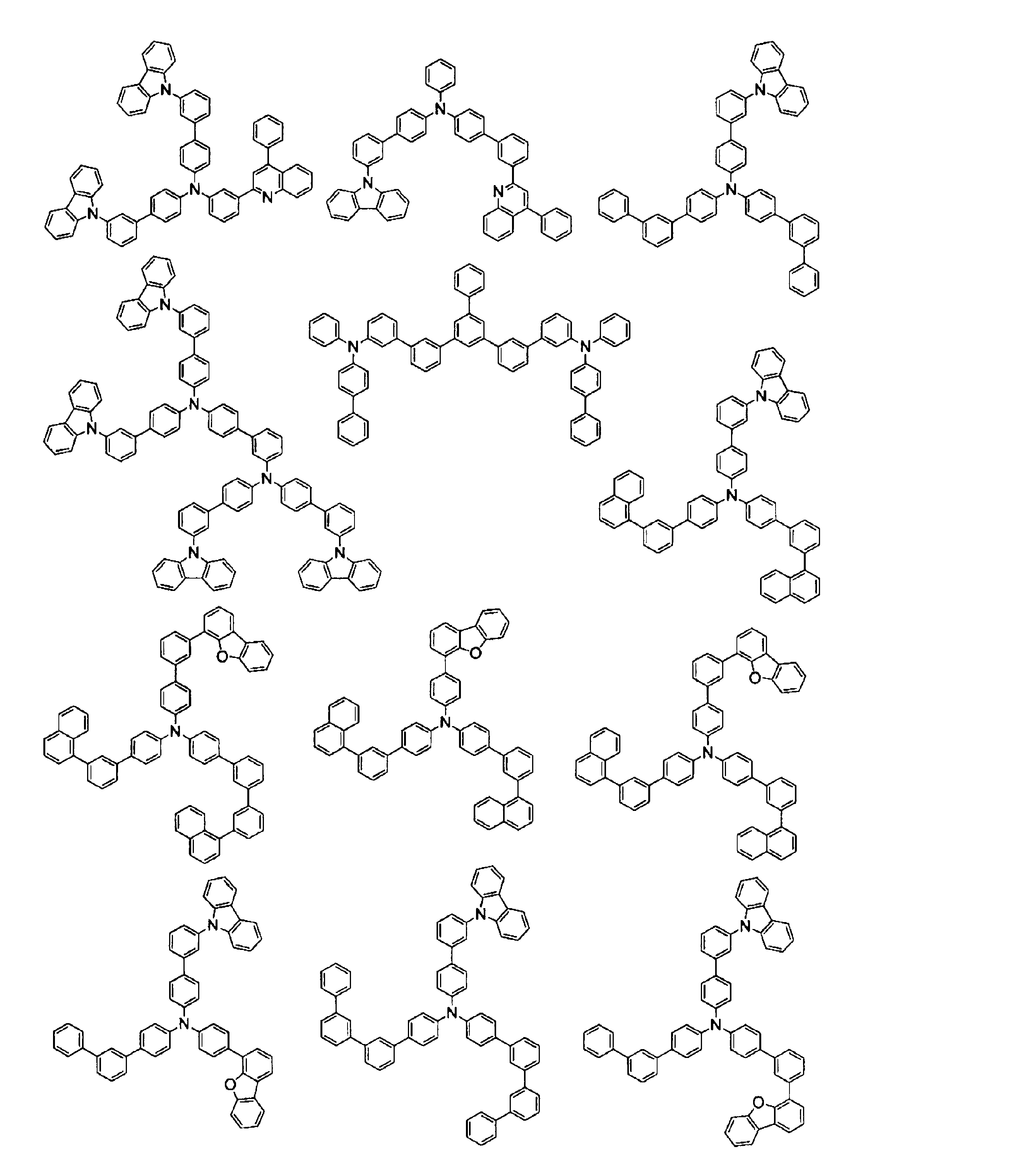

電子輸送材料としては、芳香族複素環を部分構造として有する化合物が挙げられる。芳香族複素環としては、本発明に係る1,3,5-トリアジン環のほか、例えば、ピリジン環、キノリン環、キノキサリン環、ピリミジン環などが挙げられる。
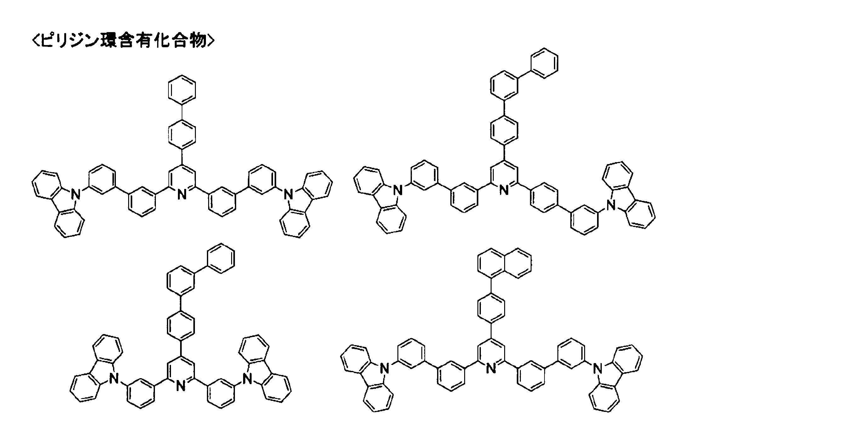

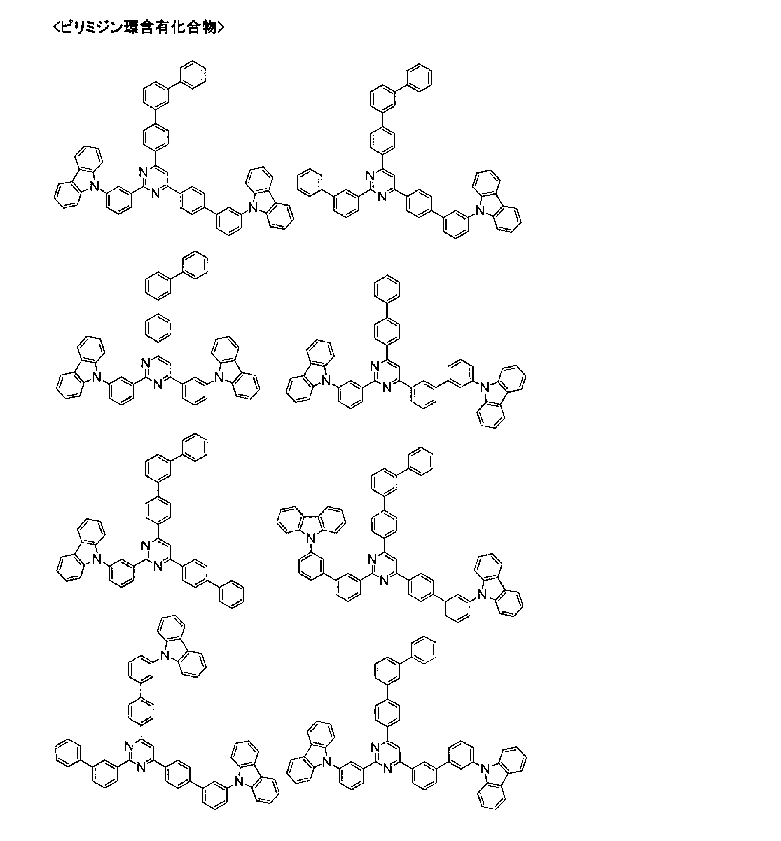
本発明の組成物は、本発明の有機化合物、溶剤、発光材料及びその他の電荷輸送材料(電子輸送材料、正孔輸送材料)以外にも、必要に応じて、更に他の成分を含有していてもよい。例えば、成膜性の向上を目的として、レベリング剤や消泡剤等の各種添加剤を含有していてもよい。また、2層以上の層を湿式成膜法により積層する際に、これらの層が相溶することを防ぐため、成膜後に硬化させて不溶化させる目的で、光硬化性樹脂や熱硬化性樹脂を含有させておくこともできる。
本発明の組成物中の電荷輸送材料、発光材料及び必要に応じて添加可能な成分(レベリング剤など)などの全材料(固形分)濃度は、通常0.01重量%以上、好ましくは0.05重量%以上、より好ましくは0.1重量%以上、さらに好ましくは0.5重量%以上、最も好ましくは1重量%以上であり、通常80重量%以下、好ましくは50重量%以下、より好ましくは40重量%以下、さらに好ましくは30重量%以下、最も好ましくは20重量%以下である。この濃度が上記下限を下回ると、成膜に際して、厚膜を形成することが困難となり、上記上限を超えると、薄膜を形成することが困難となる。
(水分濃度)
本発明の組成物を用いて湿式成膜法により層形成して、有機電界発光素子をはじめとする有機デバイスを製造する場合、用いる組成物中に水分が存在すると、形成された薄膜に水分が混入して薄膜の均一性が損なわれるため、本発明の組成物中の水分含有量はできる限り少ない方が好ましい。また一般に、有機電界発光素子をはじめとする有機デバイスは、水分により著しく劣化する材料(例えば、陰極等)が多く使用されているため、本発明の組成物中に水分が存在した場合、乾燥後の薄膜中に水分が残留し、素子の特性を低下させる可能性が考えられ好ましくない。
本発明の組成物は、湿式成膜プロセスでの安定性、例えば、インクジェット成膜法におけるノズルからの吐出安定性を高めるためには、常温で均一な液状であることが好ましい。常温で均一な液状とは、組成物が均一相からなる液体であり、かつ、組成物中に粒径0.1μm以上の粒子成分を含有しないことをいう。
本発明の組成物の粘度については、極端に低粘度の場合は、例えば成膜工程における過度の液膜流動による塗面不均一、インクジェット成膜におけるノズル吐出不良等が起こりやすくなり、極端に高粘度の場合は、インクジェット成膜におけるノズル目詰まり等が起こりやすくなる。このため、本発明の組成物の25℃における粘度は、通常2mPa・s以上、好ましくは3mPa・s以上、より好ましくは5mPa・s以上であり、通常1000mPa・s以下、好ましくは100mPa・s以下、より好ましくは50mPa・s以下である。
本発明の組成物の表面張力が高い場合は、基板に対する成膜溶液の濡れ性が低下する、液膜のレベリング性が悪く、乾燥時の成膜面乱れが起こりやすくなる、等の問題が発生するため、本発明の組成物の20℃における表面張力は、通常50mN/m未満、好ましくは40mN/m未満である。
本発明の組成物の蒸気圧が高い場合は、溶剤の蒸発による溶質濃度の変化等の問題が起こりやすくなる。このため、本発明の組成物の25℃における蒸気圧は、通常50mmHg以下、好ましくは10mmHg以下、より好ましくは1mmHg以下である。
本発明の組成物を用いて湿式成膜法により形成された薄膜は、結晶化しにくく、発光特性、耐熱性に優れた薄膜であり、通常有機電界発光素子の陰極と陽極の間の層として好適に使用される。
本発明の有機電界発光素子は、陽極、陰極、及びこれらの間に少なくとも1層の有機層を有し、該有機層のうち少なくとも1層が、本発明の組成物を用いて形成された層であることを特徴とするものであり、通常、基板上に少なくとも陽極、陰極及びこれらの両極間に設けられた発光層を有するものであって、本発明の組成物を用いて形成された層は、該発光層であることが好ましい。また、該発光層は本発明の組成物を用いて湿式成膜法により形成されることが好ましい。
基板1は有機電界発光素子の支持体となるものであり、石英やガラスの板、金属板や金属箔、プラスチックフィルムやシートなどが用いられる。特にガラス板や、ポリエステル、ポリメタクリレート、ポリカーボネート、ポリスルホンなどの透明な合成樹脂の板が好ましい。合成樹脂基板を使用する場合にはガスバリア性に留意する必要がある。基板のガスバリア性が小さすぎると、基板を通過した外気により有機電界発光素子が劣化することがあるので好ましくない。このため、合成樹脂基板の少なくとも片面に緻密なシリコン酸化膜等を設けてガスバリア性を確保する方法も好ましい方法の一つである。
基板1上には陽極2が設けられる。陽極2は発光層側の層(正孔注入層3、正孔輸送層4又は発光層5など)への正孔注入の役割を果たすものである。
この陽極2は、通常、アルミニウム、金、銀、ニッケル、パラジウム、白金等の金属、インジウム及び/又はスズの酸化物などの金属酸化物、ヨウ化銅などのハロゲン化金属、カーボンブラック、或いは、ポリ(3-メチルチオフェン)、ポリピロール、ポリアニリン等の導電性高分子などにより構成される。
陽極2の厚みは、必要とする透明性により異なる。透明性が必要とされる場合は、可視光の透過率を、通常60%以上、好ましくは80%以上とすることが望ましい。この場合、陽極の厚みは通常5nm以上、好ましくは10nm以上であり、また通常1000nm以下、好ましくは500nm以下程度である。不透明でよい場合は陽極2の厚みは任意であり、陽極2は基板1と同一でもよい。また、さらには上記の陽極2の上に異なる導電材料を積層することも可能である。
正孔注入層3は、陽極2から発光層5へ正孔を輸送する層であり、通常、陽極2上に形成される。
本発明に係る正孔注入層3の形成方法は真空蒸着法でも、湿式成膜法でもよく、特に制限はないが、ダークスポット低減の観点から正孔注入層3を湿式成膜法により形成することが好ましい。
正孔注入層3の膜厚は、通常5nm以上、好ましくは10nm以上、また、通常1000nm以下、好ましくは500nm以下の範囲である。
湿式成膜により正孔注入層3を形成する場合、通常は、正孔注入層3を構成する材料を適切な溶剤(正孔注入層用溶剤)と混合して成膜用の組成物(正孔注入層形成用組成物)を調製し、この正孔注入層形成用組成物を適切な手法により、正孔注入層3の下層に該当する層(通常は、陽極)上に塗布して成膜し、乾燥することにより正孔注入層3を形成する。
正孔注入層形成用組成物は通常、正孔注入層の構成材料として正孔輸送性化合物及び溶剤を含有する。
正孔輸送性化合物は、通常、有機電界発光素子の正孔注入層に使用される、正孔輸送性を有する化合物であれば、重合体などの高分子化合物であっても、単量体などの低分子化合物であってもよいが、高分子化合物であることが好ましい。
正孔注入層3の材料として用いられる正孔輸送性化合物は、このような化合物のうち何れか1種を単独で含有していてもよく、2種以上を含有していてもよい。2種以上の正孔輸送性化合物を含有する場合、その組み合わせは任意であるが、芳香族三級アミン高分子化合物1種又は2種以上と、その他の正孔輸送性化合物1種又は2種以上とを併用することが好ましい。
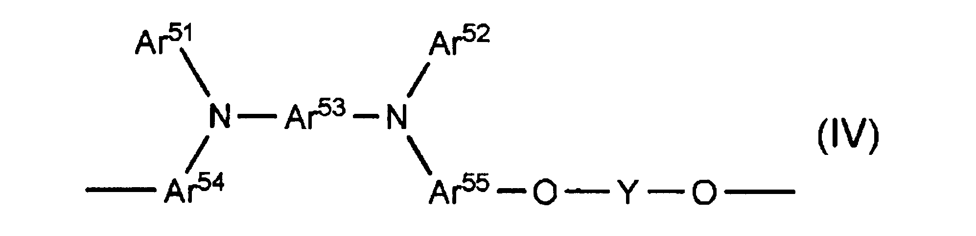
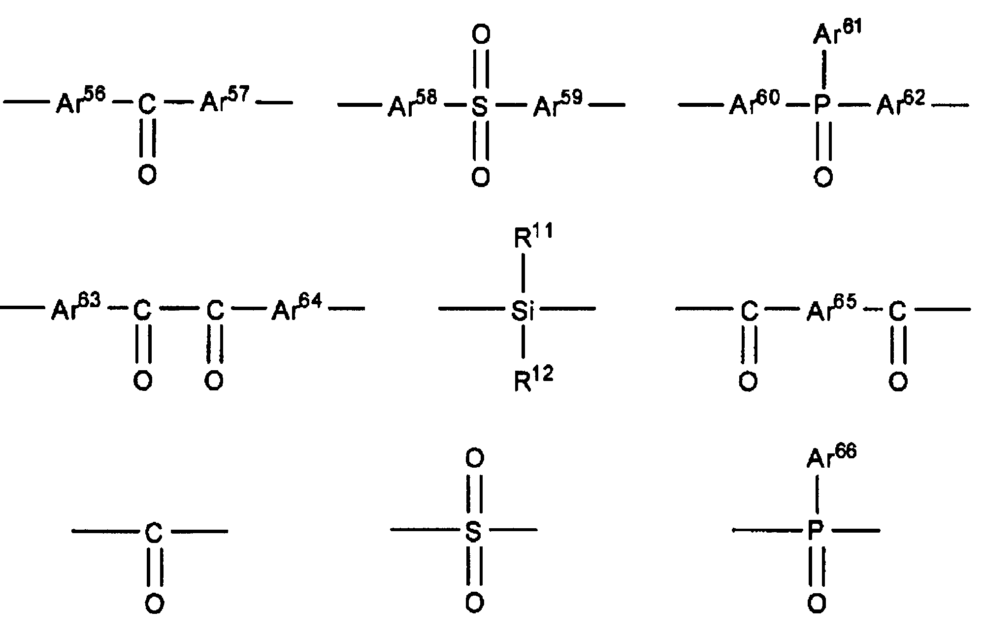
また、正孔輸送性化合物としては、ポリチオフェンの誘導体である3,4-ethylenedioxythiophene(3,4-エチレンジオキシチオフェン)を高分子量ポリスチレンスルホン酸中で重合してなる導電性ポリマー(PEDOT/PSS)もまた好ましい。また、このポリマーの末端をメタクリレート等でキャップしたものであってもよい。
さらに、正孔輸送性化合物としては、後述の「正孔輸送層」の項に記載の不溶化基を有する化合物を用いてもよい。不溶化基を有する化合物を用いる場合の成膜方法なども同様である。
正孔注入層形成用組成物は正孔注入層の構成材料として、電子受容性化合物を含有していることが好ましい。
電子受容性化合物とは、酸化力を有し、上述の正孔輸送性化合物から一電子受容する能力を有する化合物が好ましく、具体的には、電子親和力が4eV以上である化合物が好ましく、5eV以上の化合物である化合物がさらに好ましい。
正孔注入層或いは正孔注入層形成用組成物中の電子受容性化合物の正孔輸送性化合物に対する含有量は、通常0.1モル%以上、好ましくは1モル%以上である。但し、通常100モル%以下、好ましくは40モル%以下である。
正孔注入層の材料としては、本発明の効果を著しく損なわない限り、上述の正孔輸送性化合物や電子受容性化合物に加えて、さらに、その他の成分を含有させてもよい。その他の成分の例としては、各種の発光材料、電子輸送性化合物、バインダー樹脂、塗布性改良剤などが挙げられる。なお、その他の成分は、1種のみを用いてもよく、2種以上を任意の組み合わせ及び比率で併用してもよい。
湿式成膜法に用いる正孔注入層形成用組成物の溶剤のうち少なくとも1種は、上述の正孔注入層の構成材料を溶解しうる化合物であることが好ましい。また、この溶剤の沸点は通常110℃以上、好ましくは140℃以上、中でも200℃以上、通常400℃以下、中でも300℃以下であることが好ましい。溶剤の沸点が低すぎると、乾燥速度が速すぎ、膜質が悪化する可能性がある。また、溶剤の沸点が高すぎると乾燥工程の温度を高くする必要があり、他の層や基板に悪影響を与える可能性がある。
エーテル系溶剤としては、例えば、エチレングリコールジメチルエーテル、エチレングリコールジエチルエーテル、プロピレングリコール-1-モノメチルエーテルアセタート(PGMEA)等の脂肪族エーテル;1,2-ジメトキシベンゼン、1,3-ジメトキシベンゼン、アニソール、フェネトール、2-メトキシトルエン、3-メトキシトルエン、4-メトキシトルエン、2,3-ジメチルアニソール、2,4-ジメチルアニソール等の芳香族エーテル、等が挙げられる。
これらの溶剤は1種のみを用いてもよく、2種以上を任意の組み合わせ及び比率で用いてもよい。
正孔注入層形成用組成物を調製後、この組成物を湿式成膜により、正孔注入層3の下層に該当する層(通常は、陽極2)上に塗布成膜し、乾燥することにより正孔注入層3を形成する。
塗布工程における相対湿度は、本発明の効果を著しく損なわない限り限定されないが、通常0.01ppm以上、通常80%以下である。
塗布後、通常加熱等により正孔注入層形成用組成物の膜を乾燥させる。加熱工程において使用する加熱手段の例を挙げると、クリーンオーブン、ホットプレート、赤外線、ハロゲンヒーター、マイクロ波照射などが挙げられる。中でも、膜全体に均等に熱を与えるためには、クリーンオーブン及びホットプレートが好ましい。
真空蒸着により正孔注入層3を形成する場合には、正孔注入層3の構成材料(前述の正孔輸送性化合物、電子受容性化合物等)の1種又は2種以上を真空容器内に設置されたるつぼに入れ(2種以上の材料を用いる場合は各々のるつぼに入れ)、真空容器内を適当な真空ポンプで10-4Pa程度まで排気した後、るつぼを加熱して(2種以上の材料を用いる場合は各々のるつぼを加熱して)、蒸発量を制御して蒸発させ(2種以上の材料を用いる場合は各々独立に蒸発量を制御して蒸発させ)、るつぼと向き合って置かれた基板の陽極2上に正孔注入層3を形成させる。なお、2種以上の材料を用いる場合は、それらの混合物をるつぼに入れ、加熱、蒸発させて正孔注入層3を形成することもできる。
正孔輸送層4は、正孔注入層がある場合には正孔注入層3の上に、正孔注入層3が無い場合には陽極2の上に形成することができる。また、本発明の有機電界発光素子は、正孔輸送層を省いた構成であってもよい。

中でも、ベンゼン環由来の基(フェニル基)、ベンゼン環が2環連結してなる基(ビフェニル基)及びフルオレン環由来の基(フルオレニル基)が好ましい。
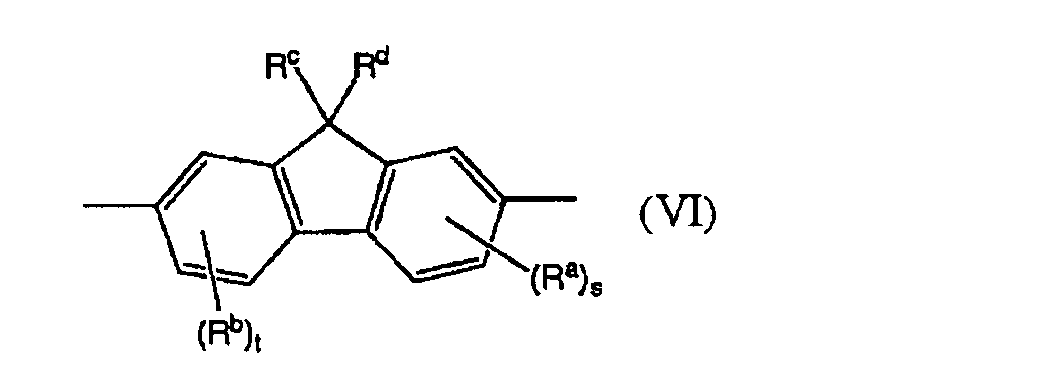
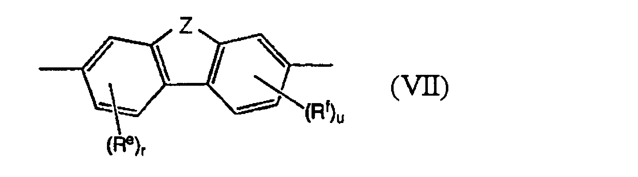
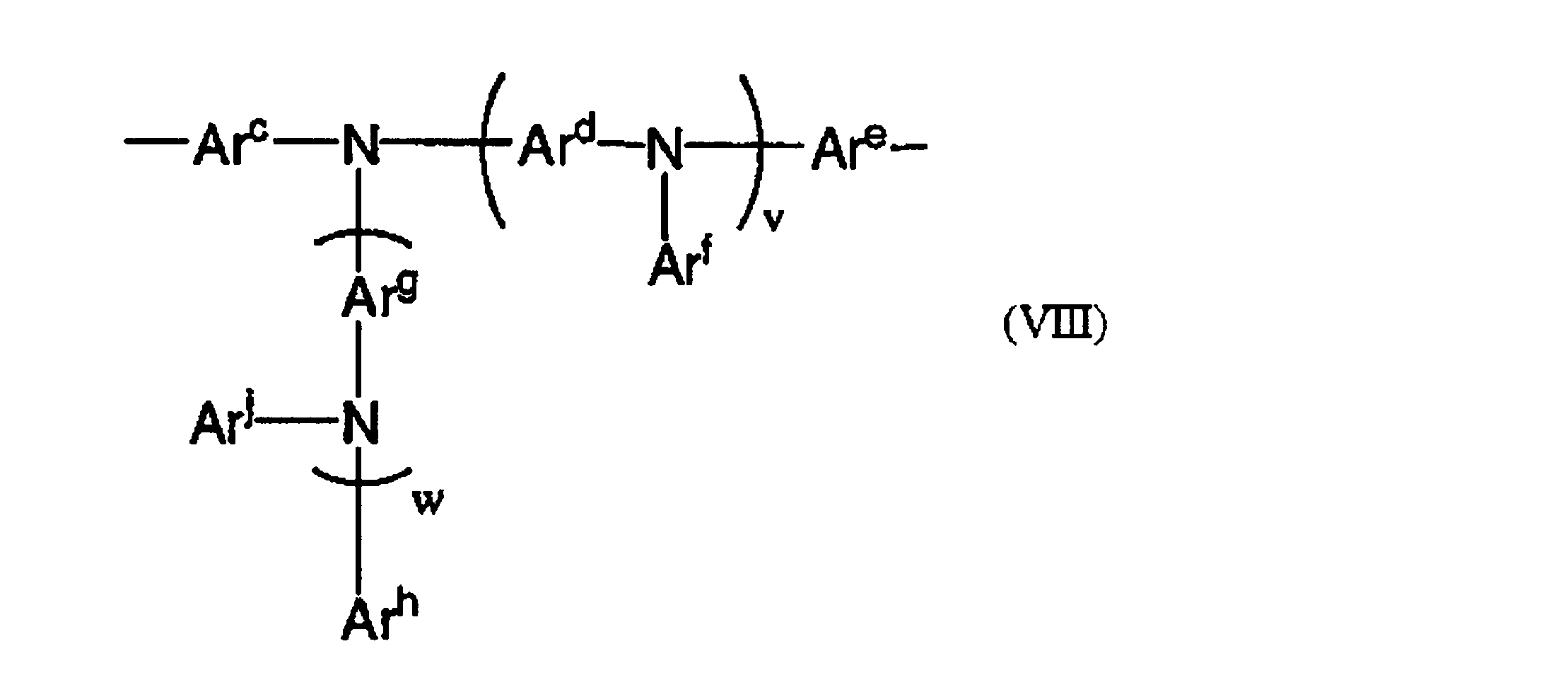
上記式(VI)~(VIII)の具体例及びポリアリーレン誘導体の具体例等は、日本国特開2008-98619号公報に記載のものなどが挙げられる。
また、さらに、レベリング剤、消泡剤等の塗布性改良剤;電子受容性化合物;バインダー樹脂などを含有していてもよい。
照射時間としては、膜の溶解性を低下させるために必要な条件を設定することが好ましいが、通常、0.1秒以上、好ましくは10時間以下照射される。
正孔輸送層4の上には通常、発光層5が設けられる。発光層5は例えば前述の発光材料を含む層であり、電界を与えられた電極間において、陽極2から正孔注入層3を通じて注入された正孔と、陰極9から電子輸送層7を通じて注入された電子との再結合により励起された、主たる発光源となる層である。発光層5は発光材料(ドーパント)と1種又は2種以上のホスト材料を含むことが好ましく、発光層5は本発明の有機化合物をホスト材料として含むことがさらに好ましい。また、発光層5は、真空蒸着法で形成してもよいが、本発明の組成物を用い、湿式製膜法によって作製された層であることが特に好ましい。
正孔阻止層6は、発光層5の上に、発光層5の陰極側の界面に接するように積層形成される。特に、発光物質として燐光材料を用いたり、青色発光材料を用いたりする場合、正孔阻止層6を設けることは効果的である。正孔阻止層6は正孔と電子を発光層5内に閉じこめて、発光効率を向上させる機能を有する。即ち、正孔阻止層6は、発光層5から移動してくる正孔が電子輸送層7に到達するのを阻止することで、発光層5内で電子との再結合確率を増やし、生成した励起子を発光層5内に閉じこめる役割と、電子輸送層7から注入された電子を効率よく発光層5の方向に輸送する役割がある。
正孔阻止層6も正孔注入層3と同様の方法で形成することができるが、通常は真空蒸着法が用いられる。
電子輸送層7は素子の発光効率をさらに向上させることを目的として、正孔注入層6と電子注入層8との間に設けられる。電子輸送層7は、電界を与えられた電極間において陰極9から注入された電子を効率よく発光層5の方向に輸送することができる化合物より形成される。電子輸送層7に用いられる電子輸送性化合物としては、陰極9又は電子注入層8からの電子注入効率が高く、かつ、高い電子移動度を有し注入された電子を効率よく輸送することができる化合物であることが必要である。
電子輸送層7は、正孔注入層3と同様にして湿式成膜法、或いは真空蒸着法により形成されるが、通常は、真空蒸着法が用いられる。
電子注入層8は陰極9から注入された電子を効率よく発光層5へ注入する役割を果たす。電子注入を効率よく行うには、電子注入層8を形成する材料は、仕事関数の低い金属が好ましく、ナトリウムやセシウム等のアルカリ金属、バリウムやカルシウムなどのアルカリ土類金属が用いられる。電子注入層8の膜厚は0.1~5nmが好ましい。
陰極9は、発光層側の層(電子注入層8又は発光層5など)に電子を注入する役割を果たす。陰極9として用いられる材料は、前記陽極2に使用される材料を用いることも可能であるが、効率よく電子注入を行うには、仕事関数の低い金属が好ましく、スズ、マグネシウム、インジウム、カルシウム、アルミニウム、銀等の適当な金属又はそれらの合金が用いられる。具体例としては、マグネシウム-銀合金、マグネシウム-インジウム合金、アルミニウム-リチウム合金等の低仕事関数合金電極が挙げられる。
以上、図1に示す層構成の素子を中心に説明してきたが、本発明の有機電界発光素子における陽極2及び陰極9と発光層5との間には、その性能を損なわない限り、上記説明にある層の他にも、任意の層を有していてもよく、また発光層5以外の任意の層を省略してもよい。
このため、電子阻止層も湿式成膜適合性を有することが好ましく、このような電子阻止層に用いられる材料としては、F8-TFBに代表されるジオクチルフルオレンとトリフェニルアミンの共重合体(国際公開第2004/084260号)等が挙げられる。
本発明の表示装置及び照明装置は、上述のような本発明の有機電界発光素子を用いたものである。本発明の表示装置及び照明装置の形式や構造については特に制限はなく、本発明の有機電界発光素子を用いて常法に従って組み立てることができる。
例えば、「有機ELディスプレイ」(オーム社、平成16年8月20日発光、時任静士、安達千波矢、村田英幸著)に記載されているような方法で、本発明の表示装置および照明装置を形成することができる。
<化合物(C-1)の合成例>
(中間体2の合成)
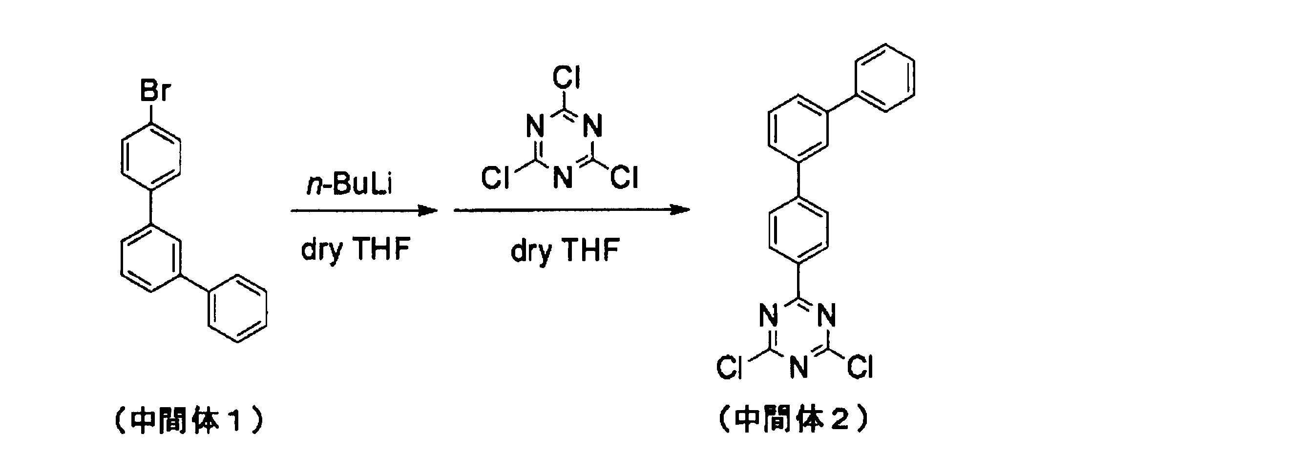
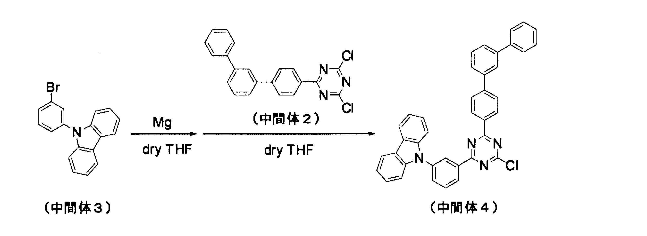
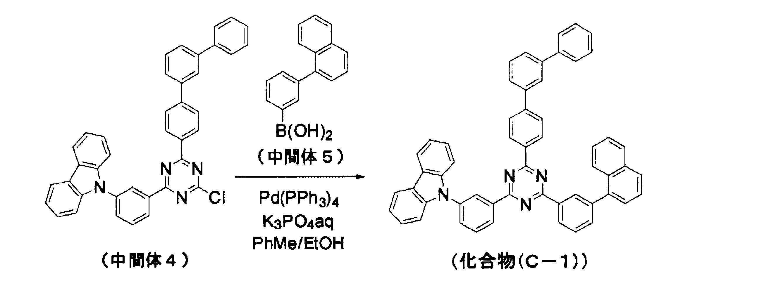
1H NMR:δ[ppm] 8.99(m、1H)、8.90-8.80(m、5H)、8.18(d、2H)、7.95-7.91(m、3H)、7.87(m、1H)、7.81-7.30(m、5H)、7.77-7.36(m、24H).
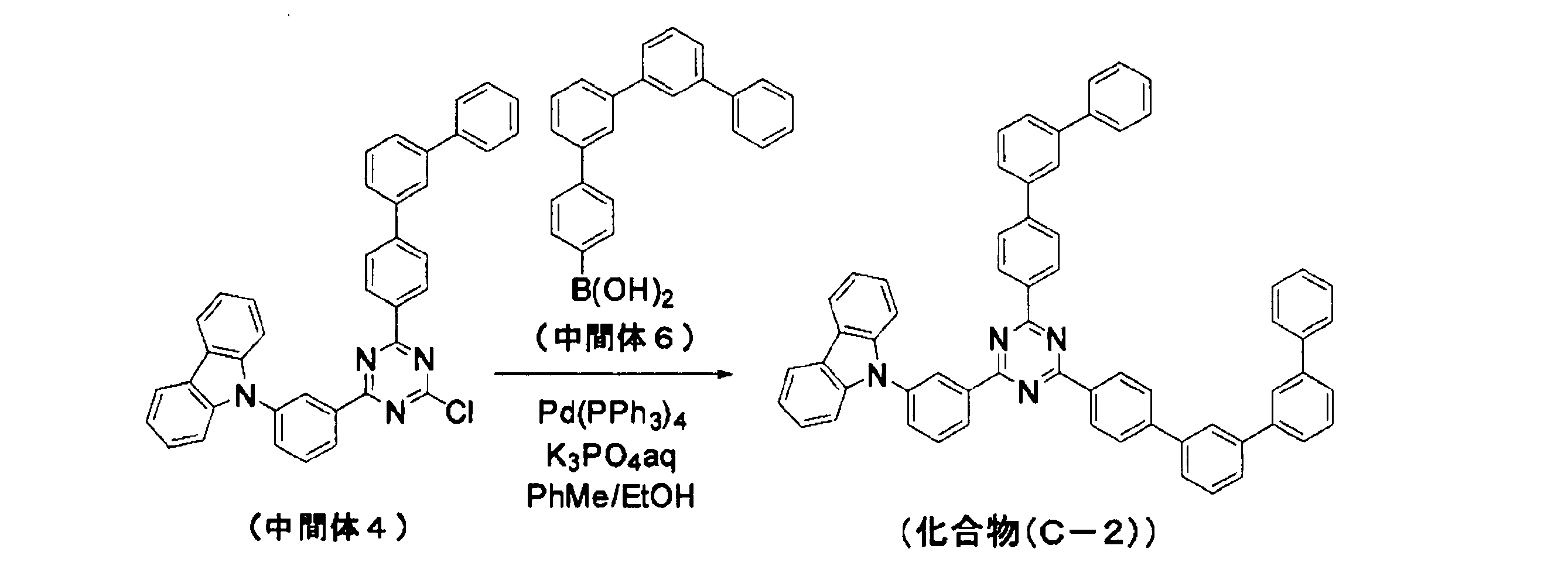
1H NMR:δ[ppm] 9.02(m、1H)、8.95-8.91(m、1H)、8.89-8.85(m、4H)、8.21(d、2H)、7.96(t、1H)、7.90(t、1H)、7.88-7.83(m、7H)、7.70-7.32(m、25H).
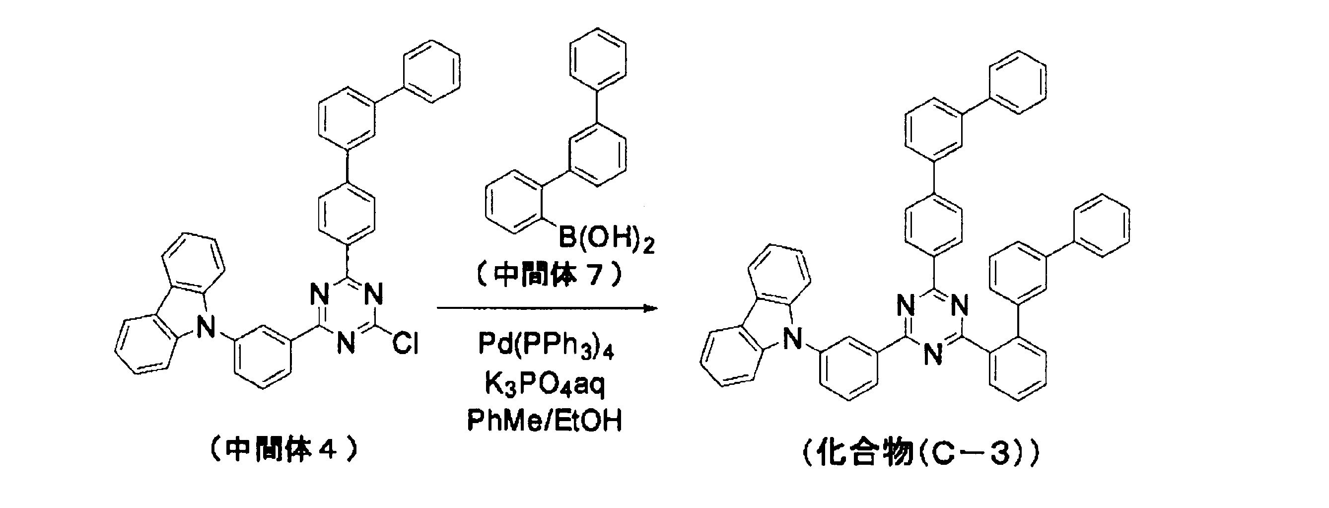
1H NMR:δ[ppm] 8.49-8.44(m、4H)、8.34(t、1H)、8.19(d、2H)、7.84(t、1H)、7.71-7.19(m、28H)、7.08-7.05(m、1H)、6.99(t、1H).
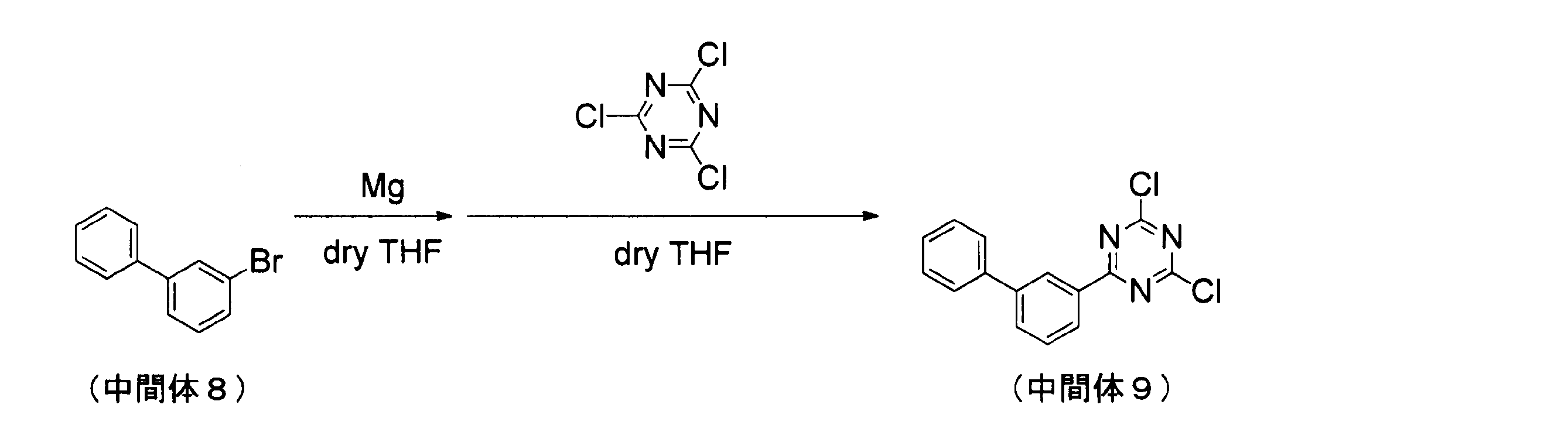
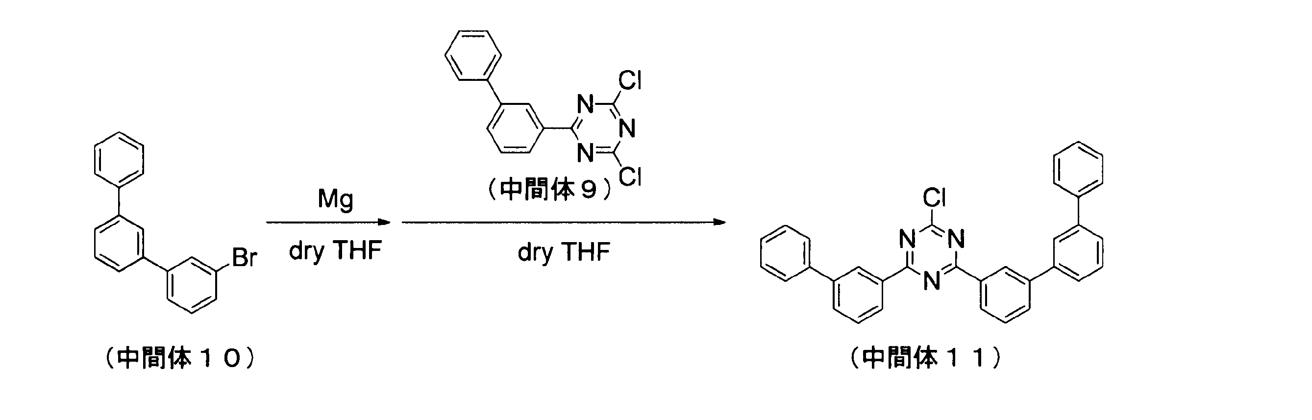
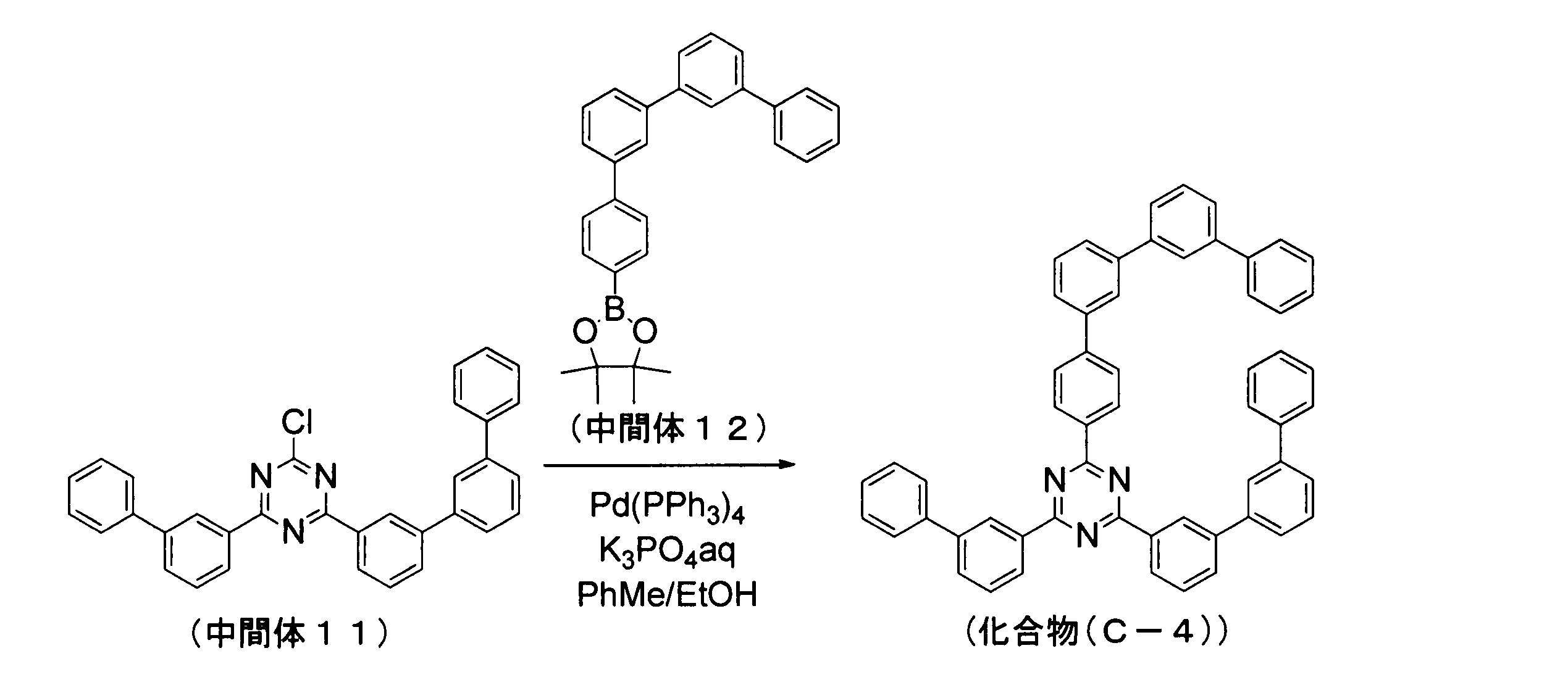
1H NMR:δ[ppm] 9.06(m、1H)、9.03(m、1H)、8.89(d、2H)、8.82-8.78(m、2H)、7.97-7.95(m、2H)、7.91-7.83(m、5H)、7.77-7.36(m、26H).
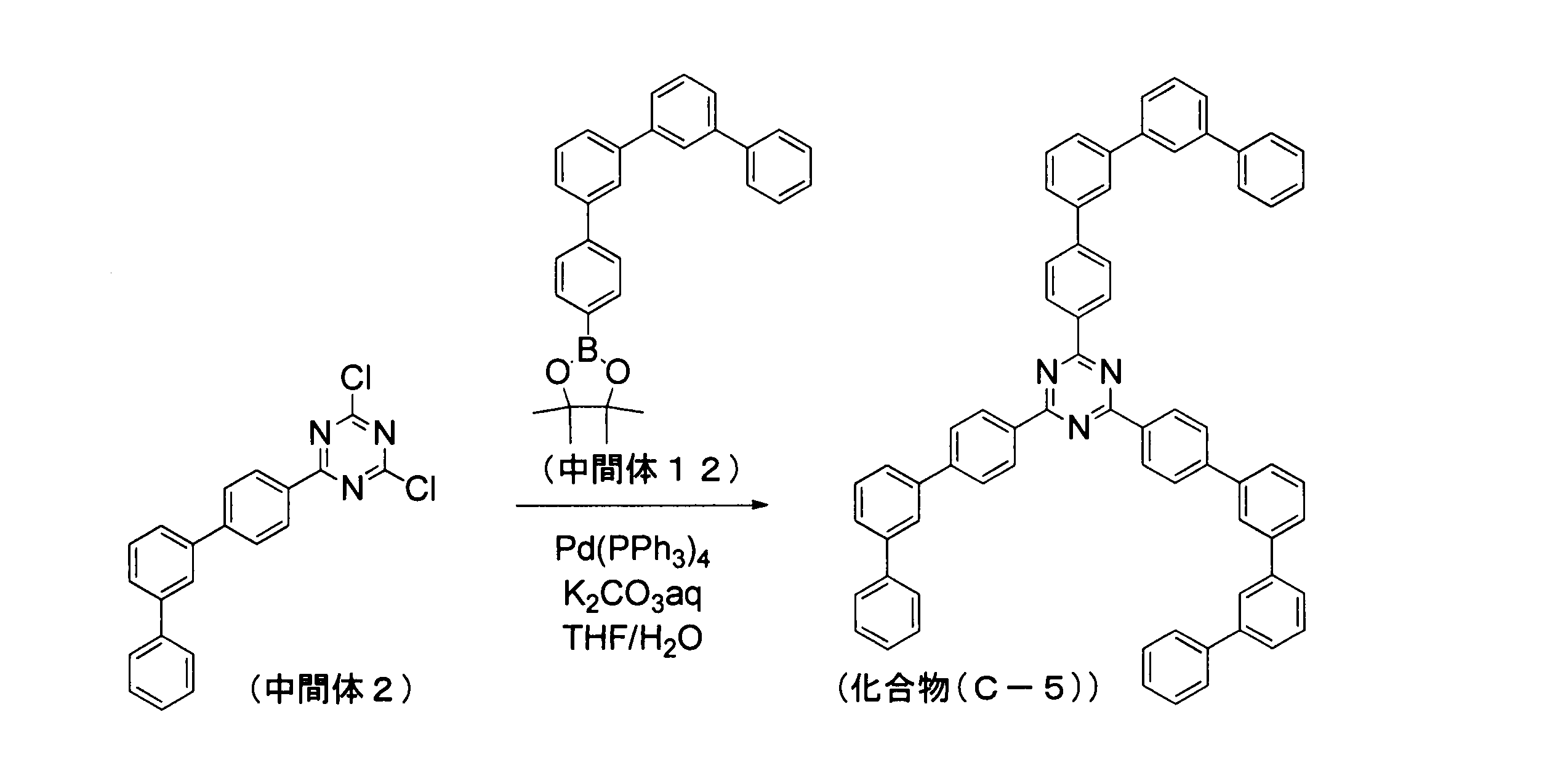
1H NMR:δ[ppm] 8.92-8.89(m、6H)、7.98(t、2H)、7.93-7.87(m、9H)、7.74-7.55(m、21H)、7.51-7.45(m、6H)、7.42-7.36(m、3H).
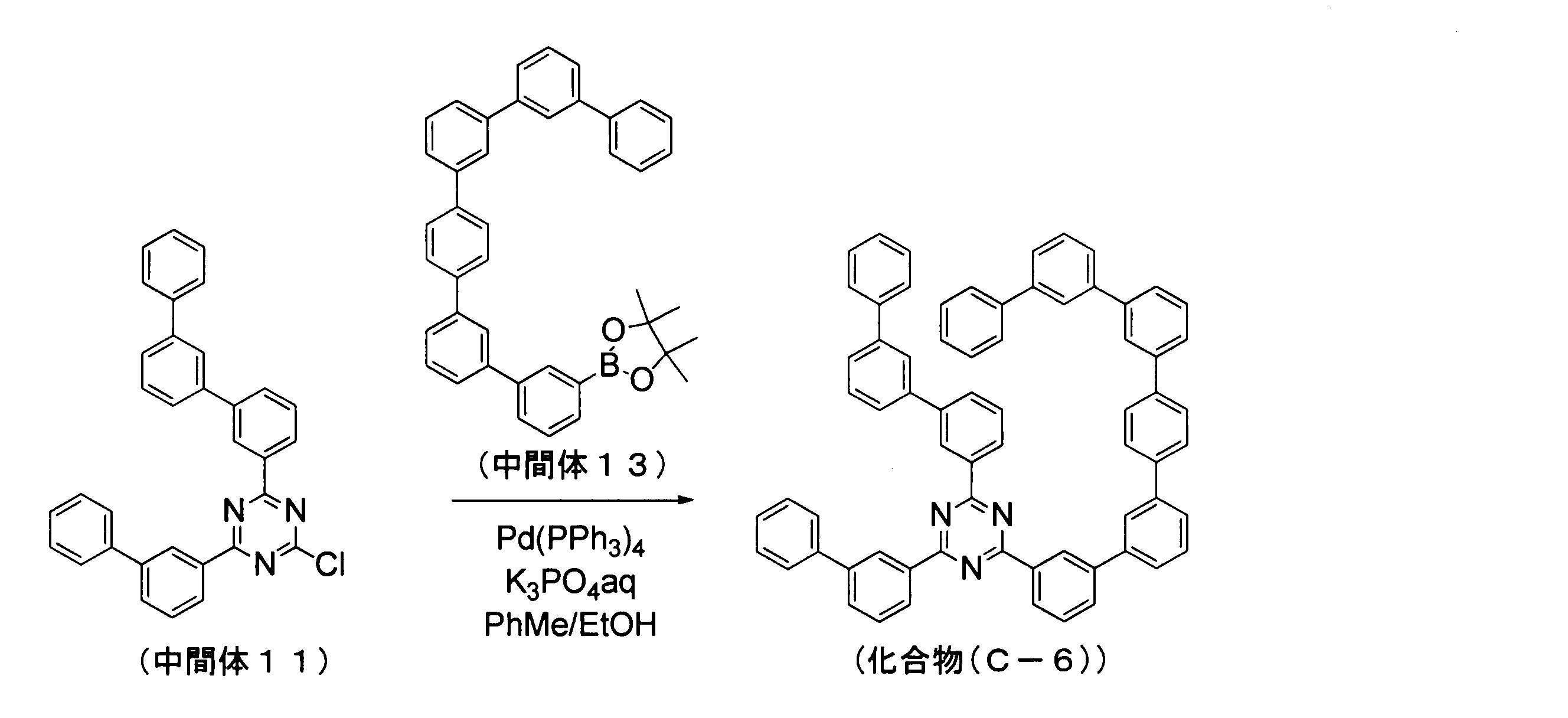
1H NMR:δ[ppm] 9.10(t、1H)、9.08(t、1H)、9.04(t、1H)、8.83-8.78(m、3H)、8.01(t、1H)、7.95-7.34(m、40H).
(中間体15の合成)
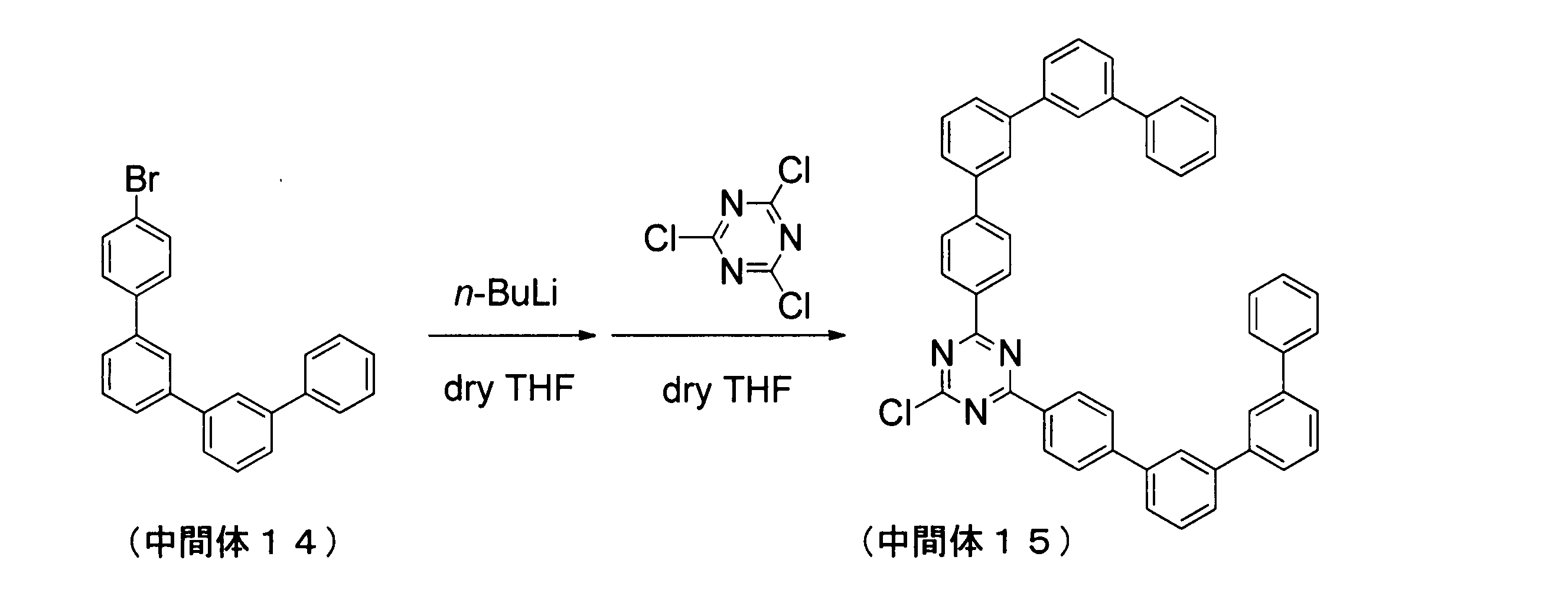
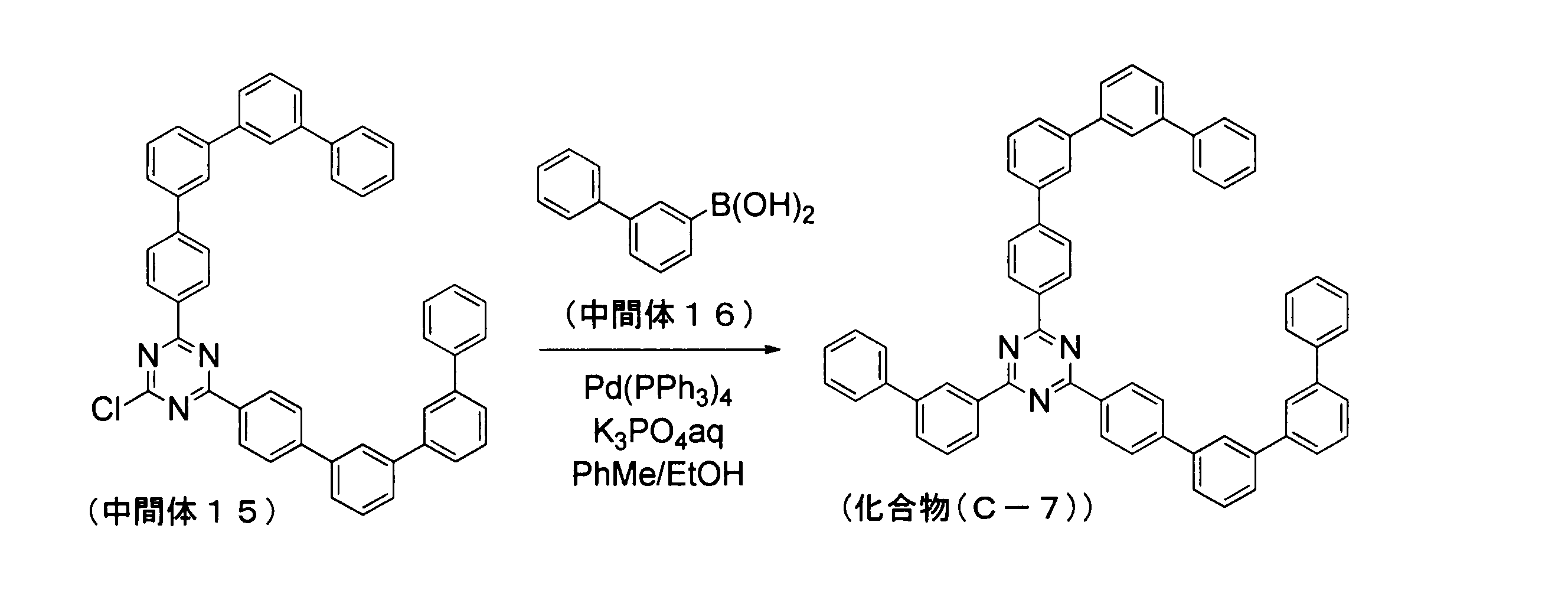
1H NMR:δ[ppm] 9.03(t、1H)、8.90(d、4H)、8.81-8.78(m、1H)、7.98(t、2H)、7.90-7.84(m、7H)、7.78-7.36(m、28H).
(中間体17の合成)
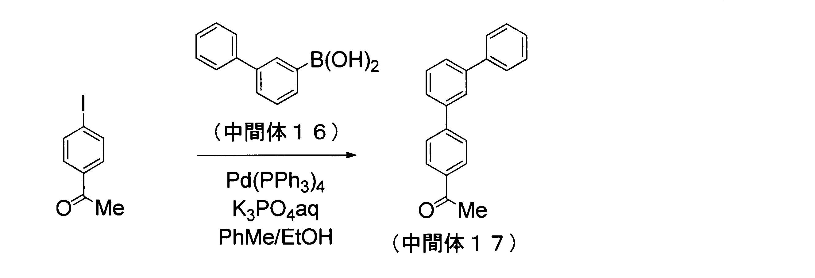

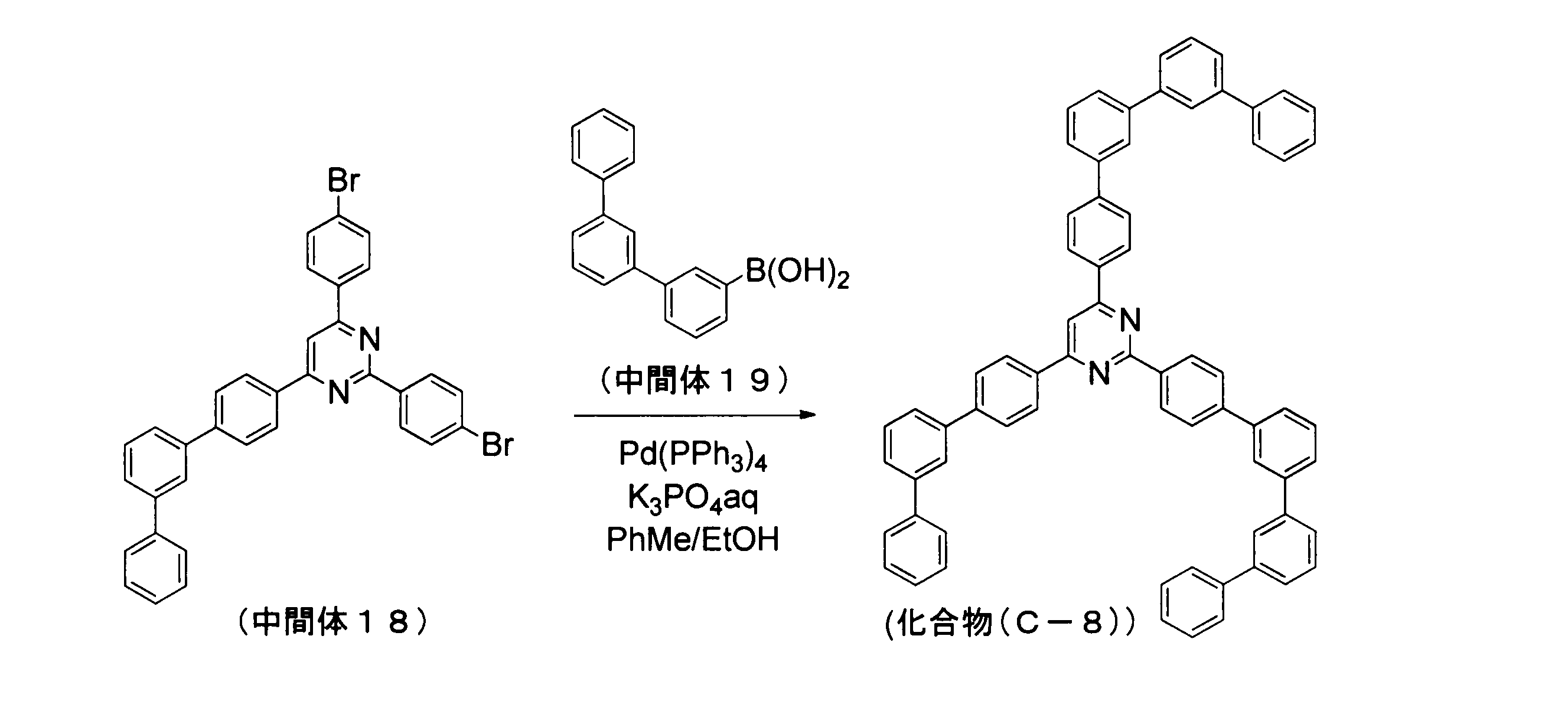
1H NMR:δ[ppm] 8.86(d、2H)、8.43(dd、4H)、8.12(s、1H)、7.98-7.95(m、2H)、7.91-7.85(m、9H)、7.73-7.54(m、21H)、7.51-7.46(m、6H)、7.42-7.36(m、3H).
(中間体21の合成例)
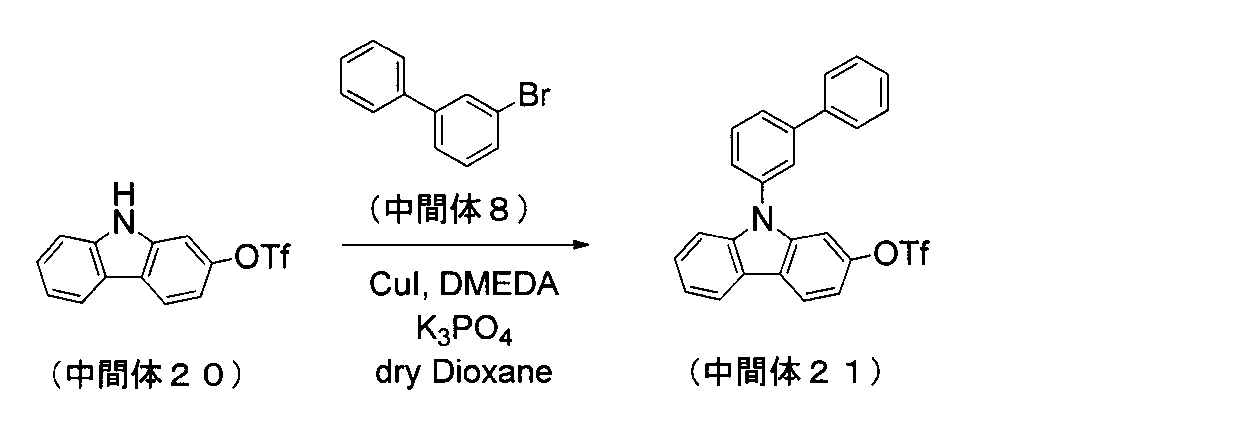
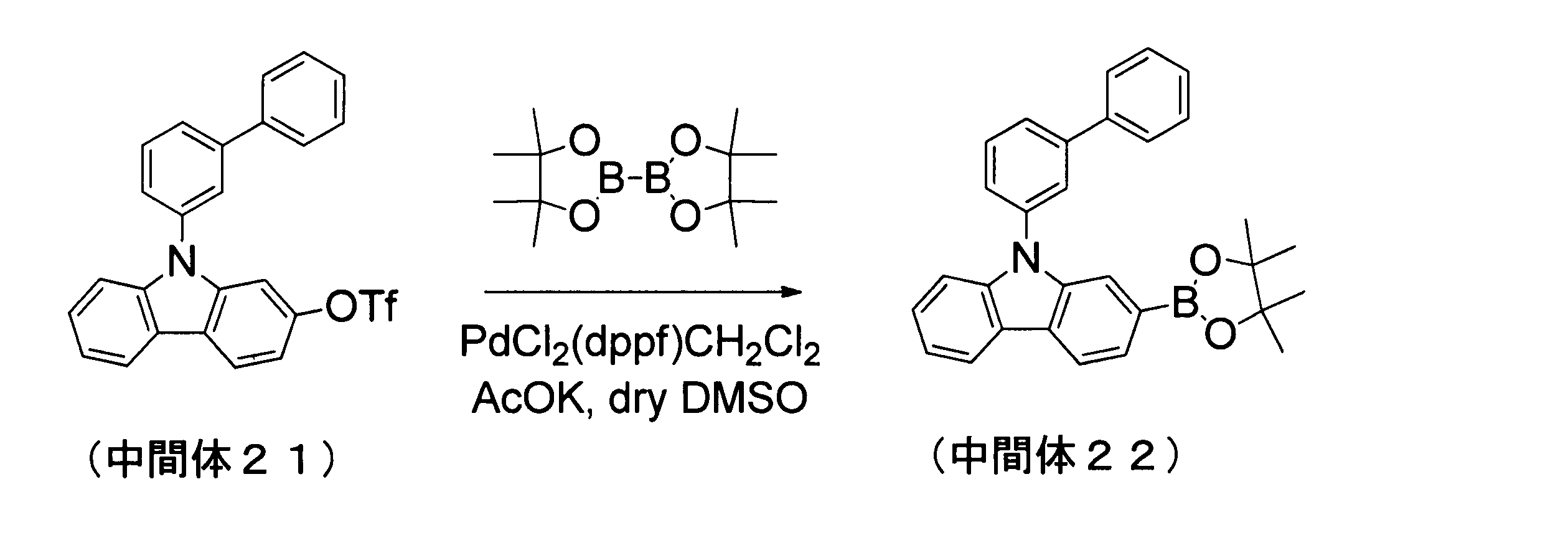
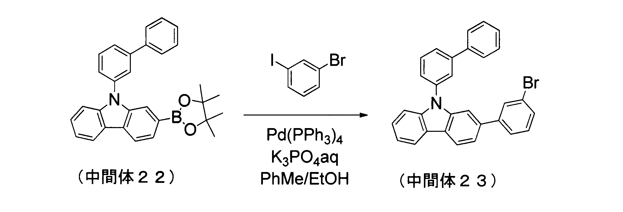
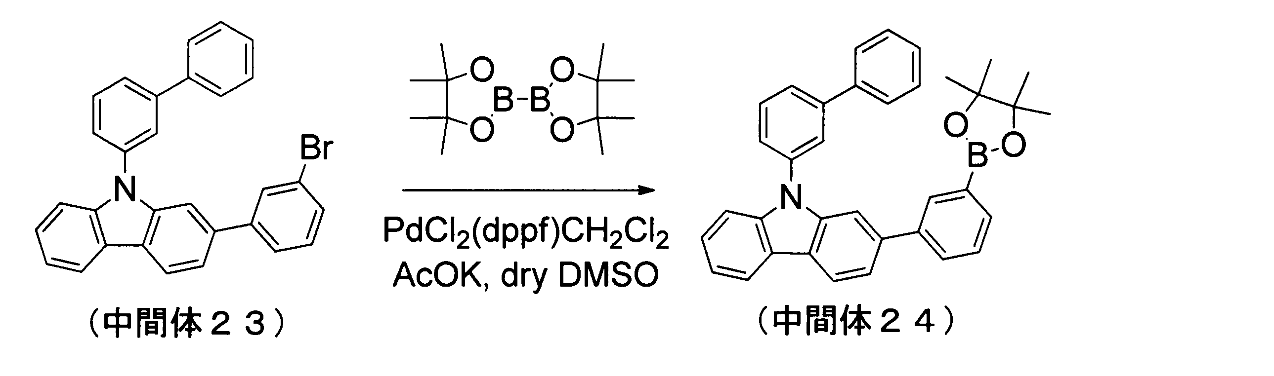
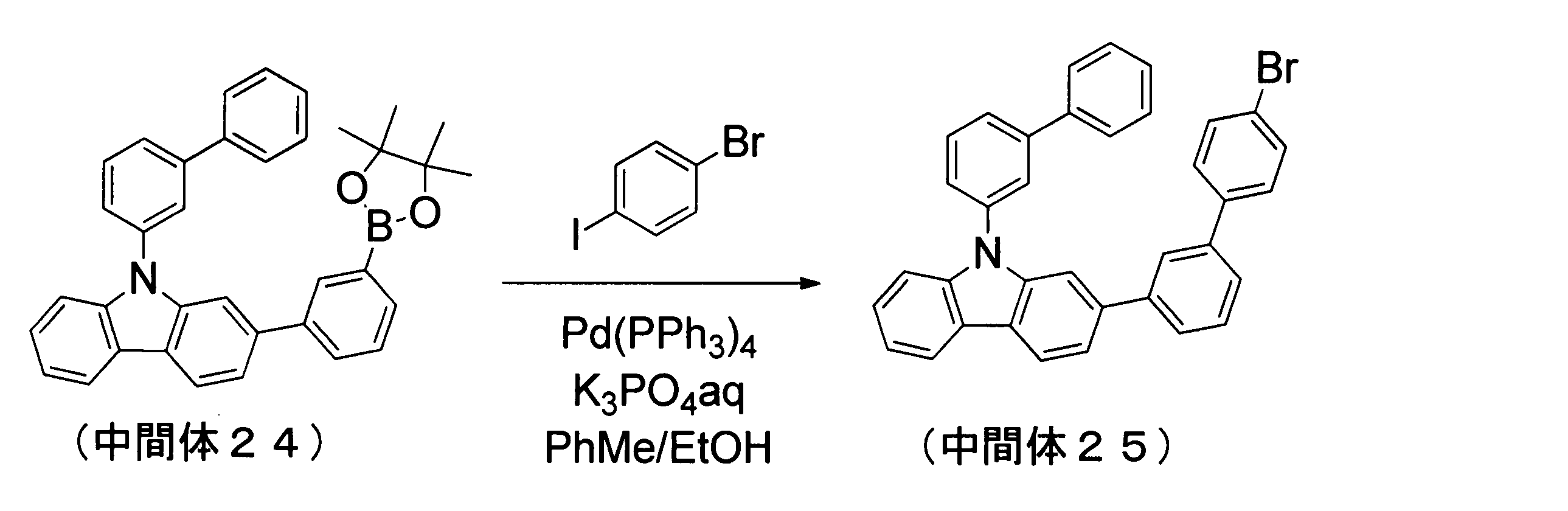
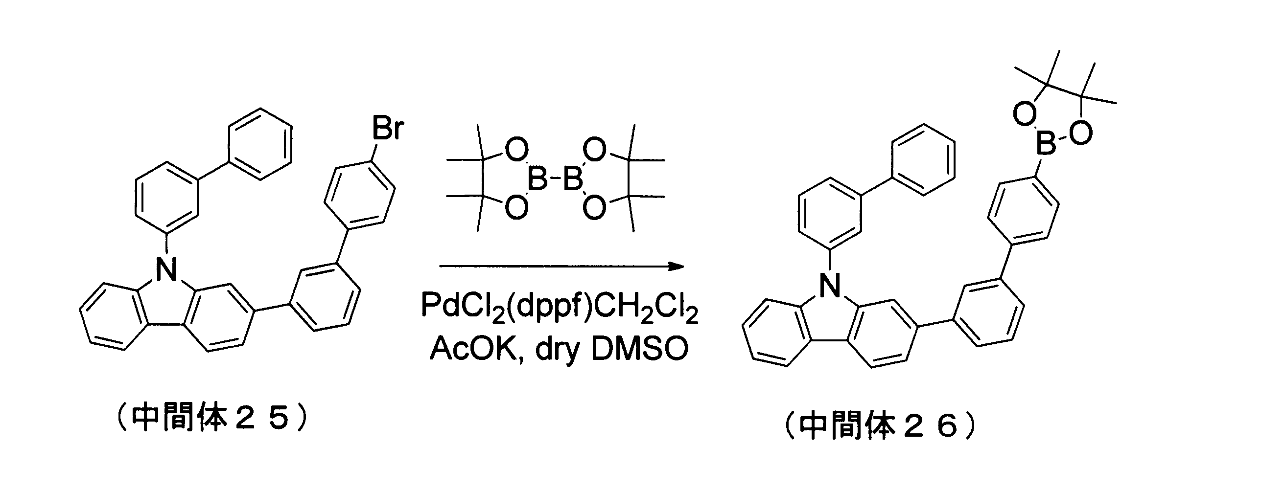
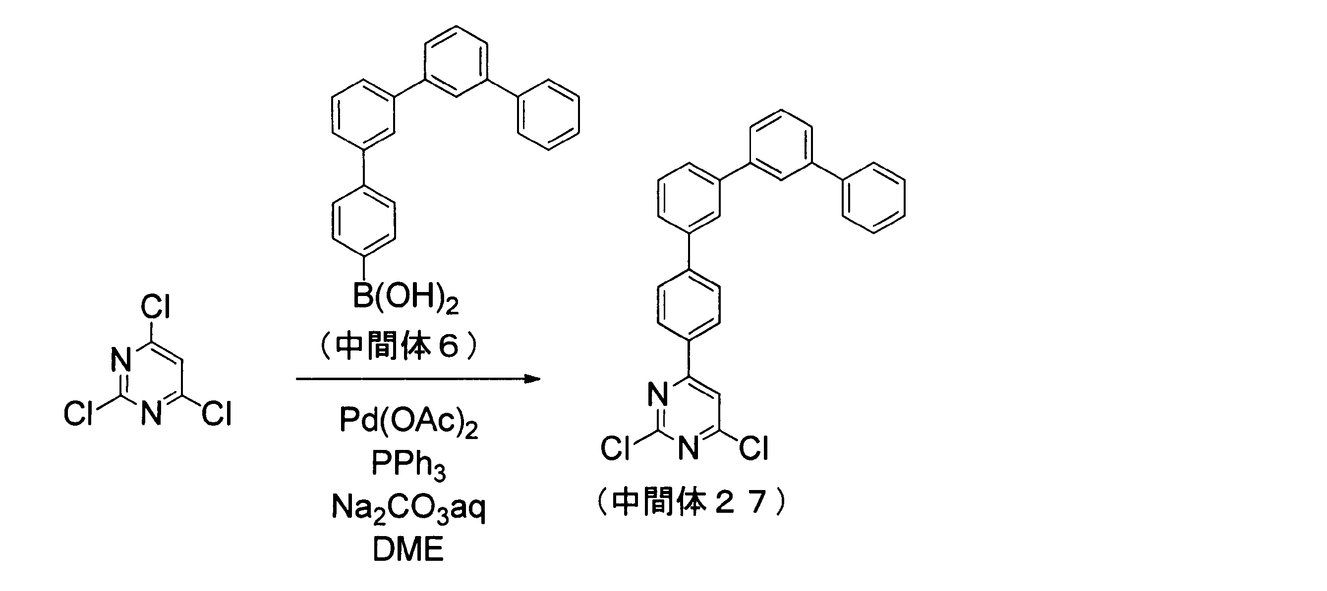
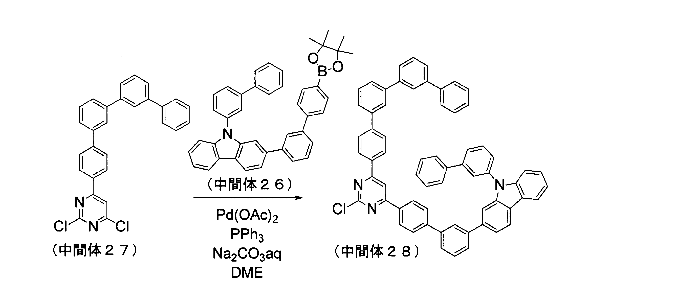
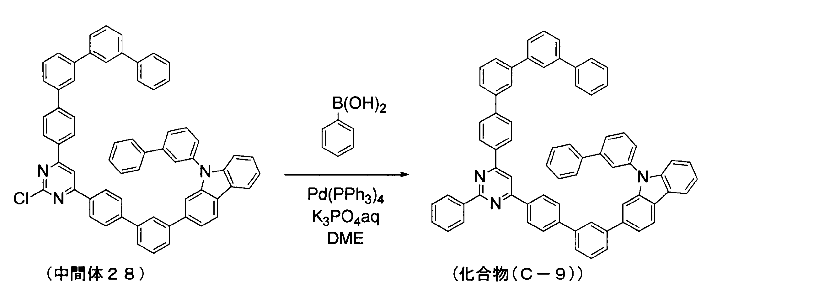
1H NMR:δ[ppm] 8.78-8.76(m、2H)、8.41(t、4H)、8.25(d、1H)、8.19(d、1H)、8.10(s、1H)、7.96-7.92(m、2H)、7.90-7.80(m、6H)、7.74-7.30(m、30H).
(中間体30の合成)

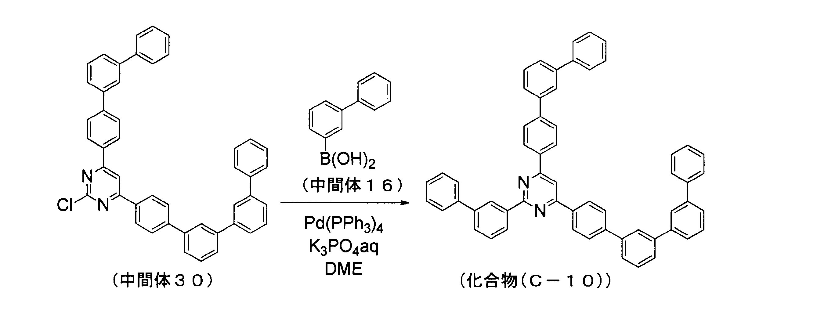
1H NMR:δ[ppm] 8.99(t、1H)、8.76-8.74(m、1H)、8.43(dd、4H)、8.13(s、1H)、7.95(t、1H)、7.91-7.85(m、6H)、7.78-7.75(m、3H)、7.71-7.46(m、20H)、7.42-7.37(m、3H).
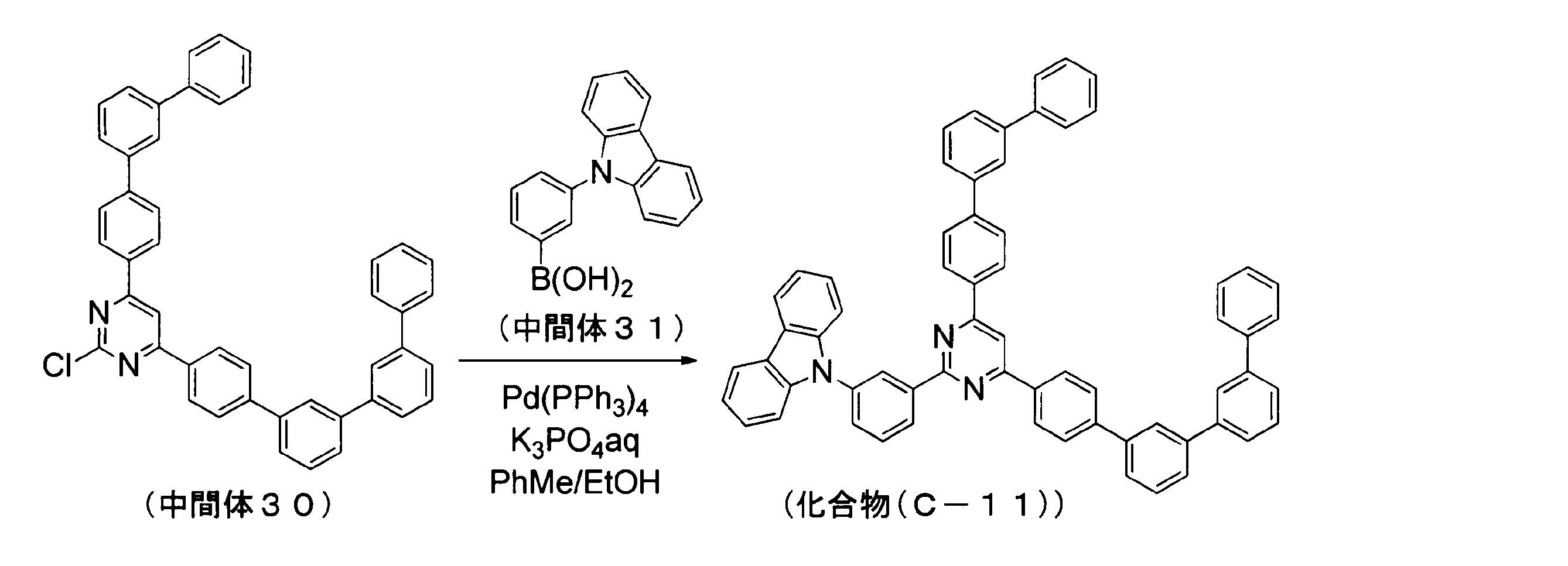
1H NMR:δ[ppm] 8.97(m、1H)、8.89-8.86(m、1H)、8.39(dd、4H)、8.19(d、2H)、8.16(s、1H)、7.93(t、1H)、7.88-7.80(m、7H)、7.74-7.30(m、26H).
比較化合物(C-12)は、国際公開第2006/62062号に示す方法にて合成した(同特許文献中にガラス転移点温度は159℃と記載してある)。
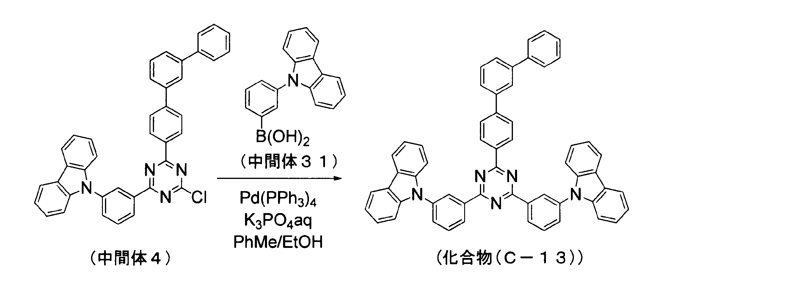
1H NMR:δ[ppm] 8.98(m、2H)、8.87-8.84(m、2H)、8.79(d、2H)、8.18(d、4H)、7.86(t、1H)、7.82-7.78(m、6H)、7.66-7.60(m、4H)、7.56-7.29(m、16H).
(中間体33の合成)
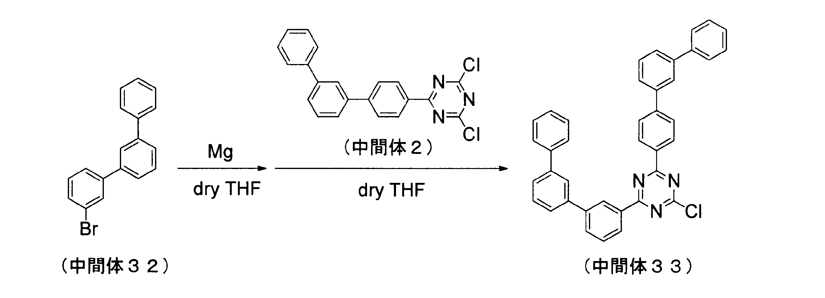
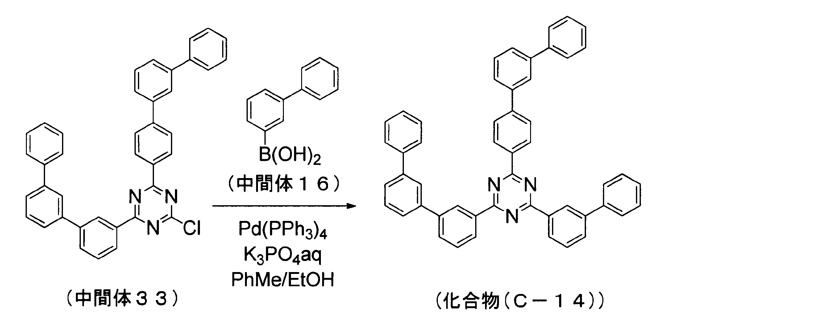
1H NMR:δ[ppm] 9.07(t、1H)、9.04(t、1H)、8.89(d、2H)、8.83-8.79(m、2H)、7.96-7.84(m、6H)、7.77-7.55(m、14H)、7.52-7.47(m、6H)、7.44-7.37(m、3H).
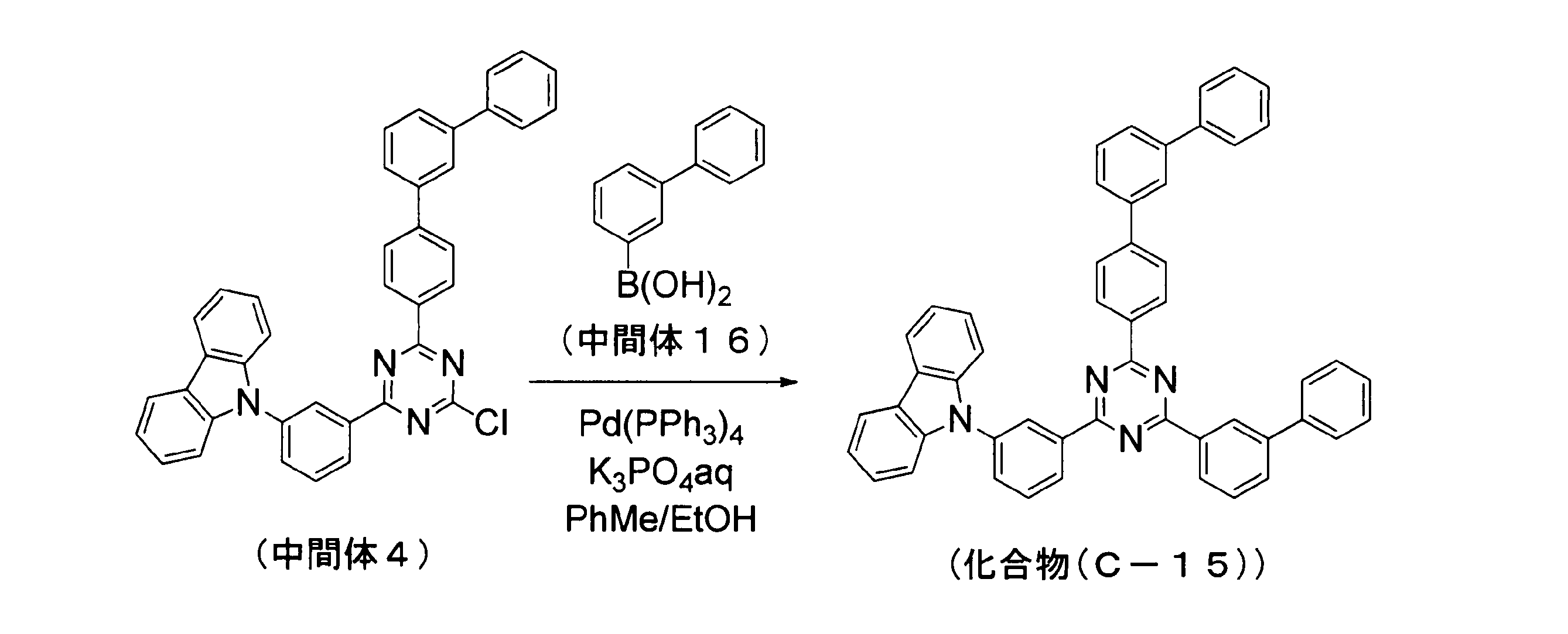
1H NMR:δ[ppm] 9.02(m、1H)、9.00(m、1H)、8.92-8.89(m、1H)、8.85(d、2H)、8.77-8.74(m、1H)、8.20(d、2H)、7.90(t、1H)、7.86-7.83(m、5H)、7.74-7.72(m、2H)、7.68-7.62(m、5H)、7.58-7.32(m、13H).
(中間体35の合成)
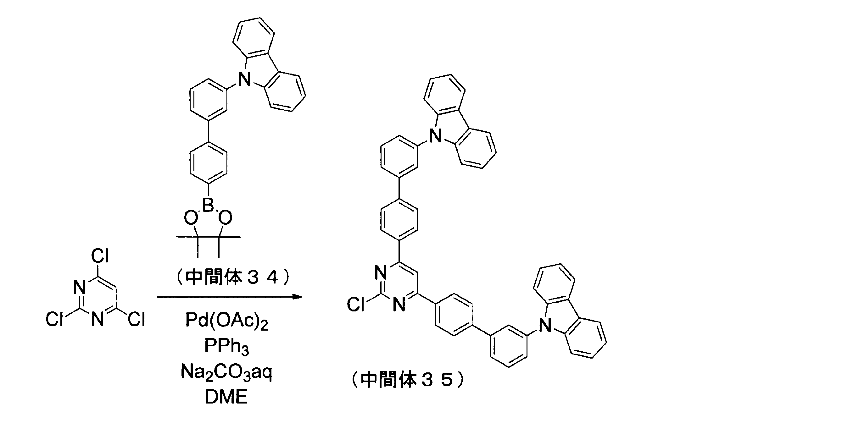
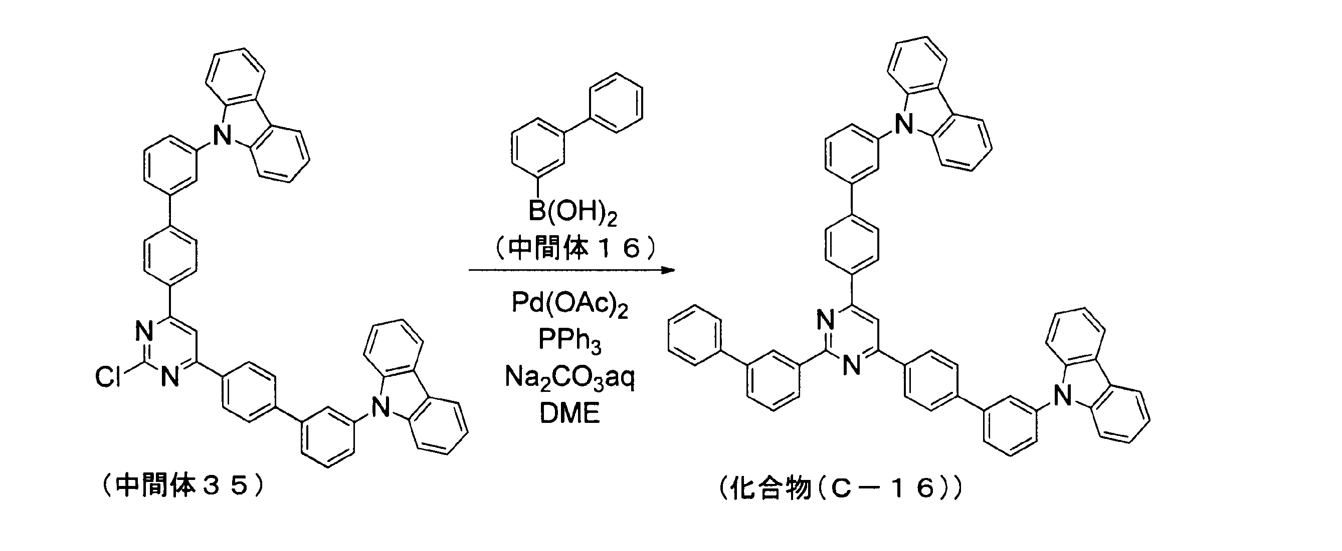
1H NMR:δ[ppm] 8.97(m、1H)、8.75-8.72(m、1H)、8.42(d、4H)、8.17(d、4H)、8.10(s、1H)、7.91-7.71(m、13H)、7.65-7.60(m、3H)、7.52-7.37(m、11H)、7.33-7.29(m、4H).
(中間体37の合成)
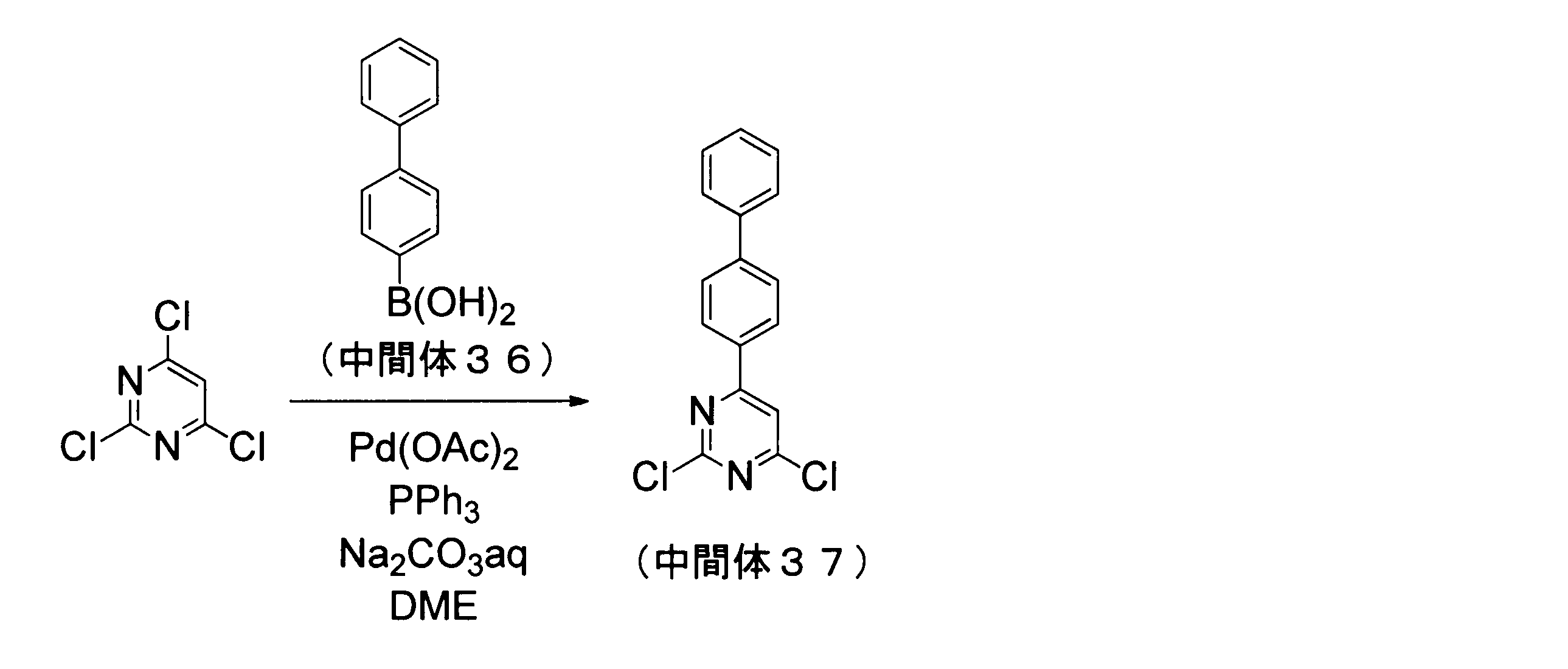
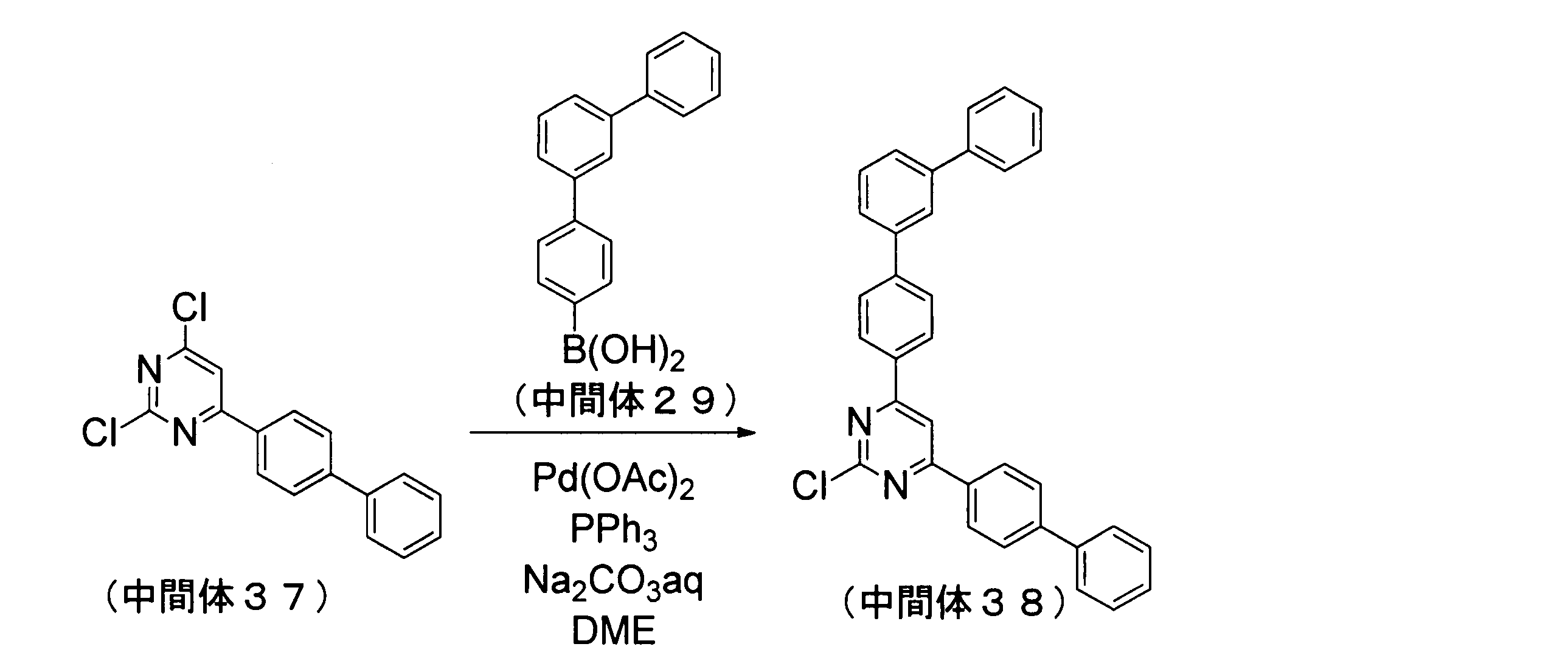

1H NMR:δ[ppm] 8.96(t、1H)、8.88-8.86(m、1H)、8.39-8.36(m、4H)、8.19(d、2H)、8.14(s、1H)、7.87(t、1H)、7.83-7.61(m、12H)、7.57-7.30(m、13H).
前記例示化合物に含まれる以下の化合物について、下記に示す方法により有機溶剤に溶解し、組成物を調製した。なお、化合物(C-18)は、日本国特開2006-188493号公報にて開示された方法を参考にして得た。

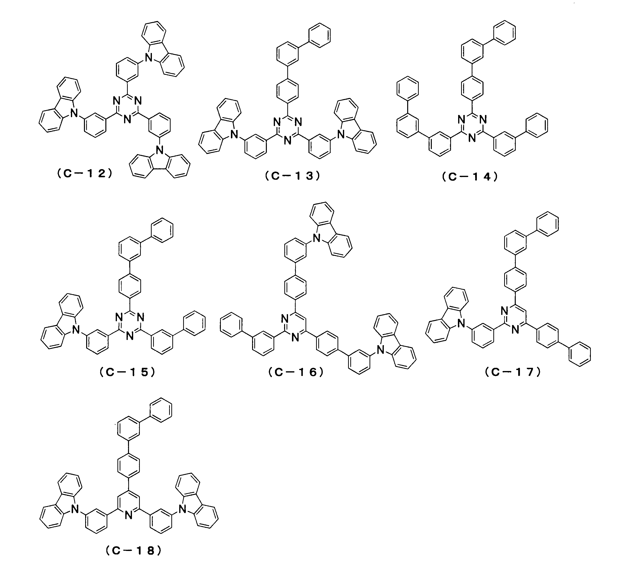
5mLのサンプル管に、化合物(C-1)を5mg量りとり、シクロへキシルベンゼンを加えて400mgとした後、ホットプレートを用いて60℃に加熱し、化合物(C-1)を完全に溶解させ、固形分1.25重量%濃度の組成物を調製した。調製した組成物は、室温約15~20℃の暗所に置き、固体が析出するまでの時間を測定した。固体の析出は10倍のルーペを用いて目視にて確認した。結果を化合物(C-1)の分子量、ガラス転移点温度と共に表1にまとめた。
実施例1において化合物(C-1)を化合物(C-2)~(C-11)にそれぞれ置き換えたほかは、実施例1と同様に組成物を調製し、固体が析出するまでの時間を測定した。固体の析出は10倍のルーペを用いて目視にて確認した。結果を化合物(C-2)~(C-11)の分子量、ガラス転移点温度と共に表1にまとめた。
実施例1において化合物(C-1)を比較化合物(C-12)~(C-17)に置き換えたほかは、実施例1と同様に組成物の調製を試みた。このうち、比較化合物(C-12)、(C-15)および(C-16)については、ホットプレートによる加熱を30分行ったが、サンプル管の底に固形分が残留しているのが確認され、1.25重量%濃度の組成物を調製することができなかった。組成物が調製できたものについては、実施例1と同様の方法にて固体が析出するまでの時間を測定した。固体の析出は10倍のルーペを用いて目視にて確認した。結果を化合物(C-12)~(C-17)の分子量、カルバゾリル基の数、ガラス転移点温度と共に表1にまとめた。
実施例1において化合物(C-1)を化合物(C-18)に置き換えたほかは、実施例1と同様に組成物を調製し、固体が析出するまでの時間を測定した。固体の析出は10倍のルーペを用いて目視にて確認した。結果を化合物(C-18)の分子量、カルバゾリル基の数、ガラス転移点温度と共に表1にまとめた。なお、化合物(C-18)は、ピリジン骨格の化合物であるため、本発明の範囲外となるが、1,3,5-トリアジン骨格の溶解性の低さの比較をおこなうために参考として示す。
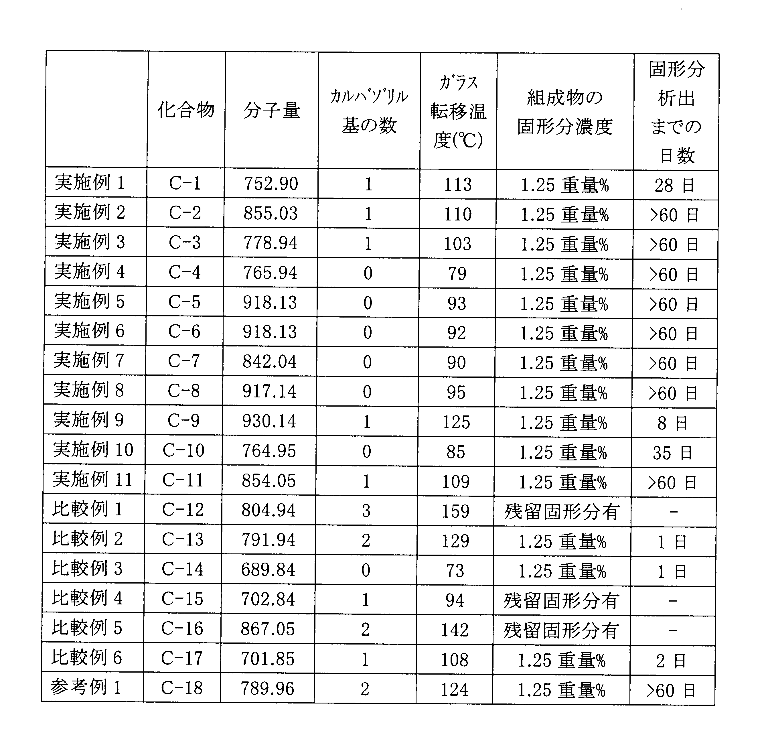
<実施例12>
以下の手順で図1に示す有機電界発光素子を作製した。
ガラス基板1上に、インジウム・スズ酸化物(ITO)透明導電膜を70nmの厚さに堆積したもの(ジオマテック社製、スパッタ成膜品)を、通常のフォトリソグラフィー技術と塩酸エッチングを用いて2mm幅のストライプにパターニングして陽極2を形成した。パターン形成したITO基板を、界面活性剤水溶液による超音波洗浄、超純水による水洗、超純水による超音波洗浄、超純水による水洗の順で洗浄後、圧縮空気と接触させることにより乾燥させてから、紫外線オゾン洗浄を行った。
次に、以下の構造式(HIT-1)に示すアリールアミンポリマー、構造式(A-1)に示す4-イソプロピル-4’-メチルジフェニルヨードニウムテトラキス(ペンタフルオロフェニル)ボラートおよび安息香酸エチルを含有する正孔注入輸送層形成用塗布液を調製した。この塗布液を下記条件で陽極上にスピンコート法により成膜し、膜厚30nmの正孔注入輸送層3を形成した。

溶剤 安息香酸エチル
塗布液濃度 HIT-1:2.0重量%
A-1 :0.4重量%
<正孔注入輸送層3の成膜条件>
スピナ回転時間 30秒
スピンコート雰囲気 大気中
加熱条件 大気中、230℃、1時間
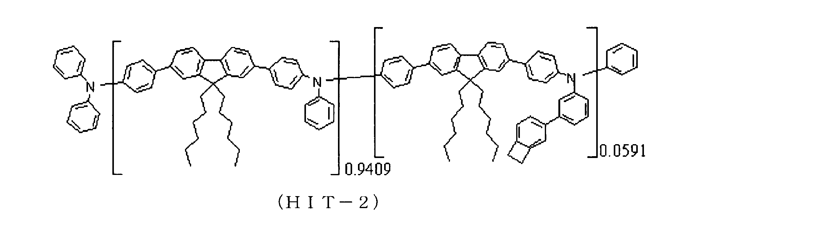
溶剤 シクロヘキシルベンゼン
塗布液濃度 HIT-2:1.0重量%
<正孔注入輸送層4の成膜条件>
スピナ回転時間 120秒
スピンコート雰囲気 乾燥窒素中
加熱条件 230℃、1時間、窒素中
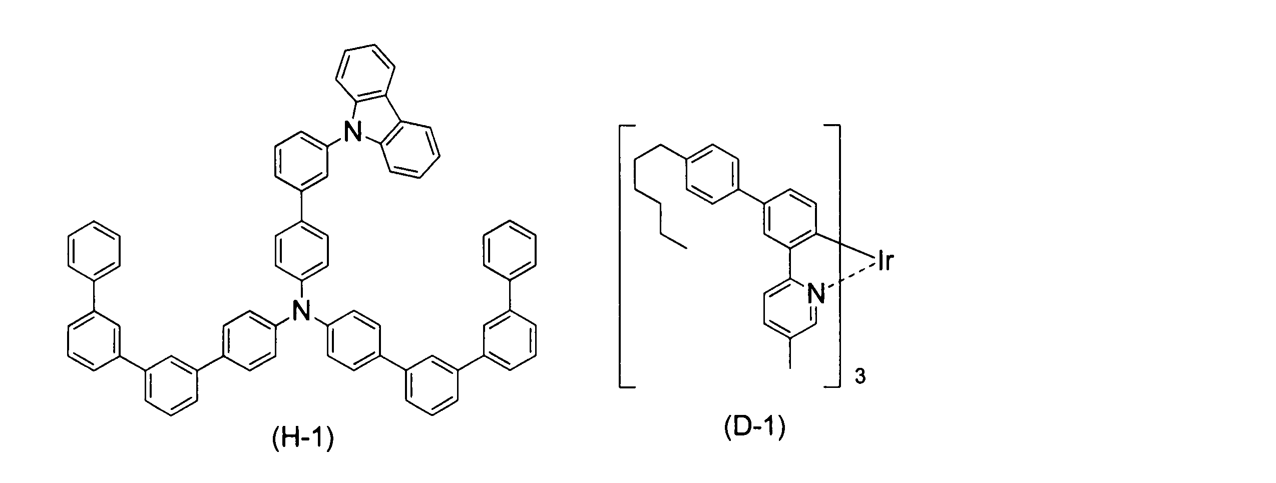
溶剤 シクロヘキシルベンゼン
塗布液濃度 C-1:1.2重量%
H-1:3.6重量%
D-1:0.48重量%
<発光層5の成膜条件>
スピナ回転時間 120秒
加熱条件 120℃、20分
この発光層5まで成膜した基板を真空蒸着装置内に移し、装置内の真空度が2.0×10⁻⁴Pa以下になるまで排気した後、以下の構造式(HB-1)に示す化合物を真空蒸着法にて、蒸着速度0.8~1.2Å/秒で発光層5の上に積層させ、膜厚10nmの正孔阻止層6を得た。
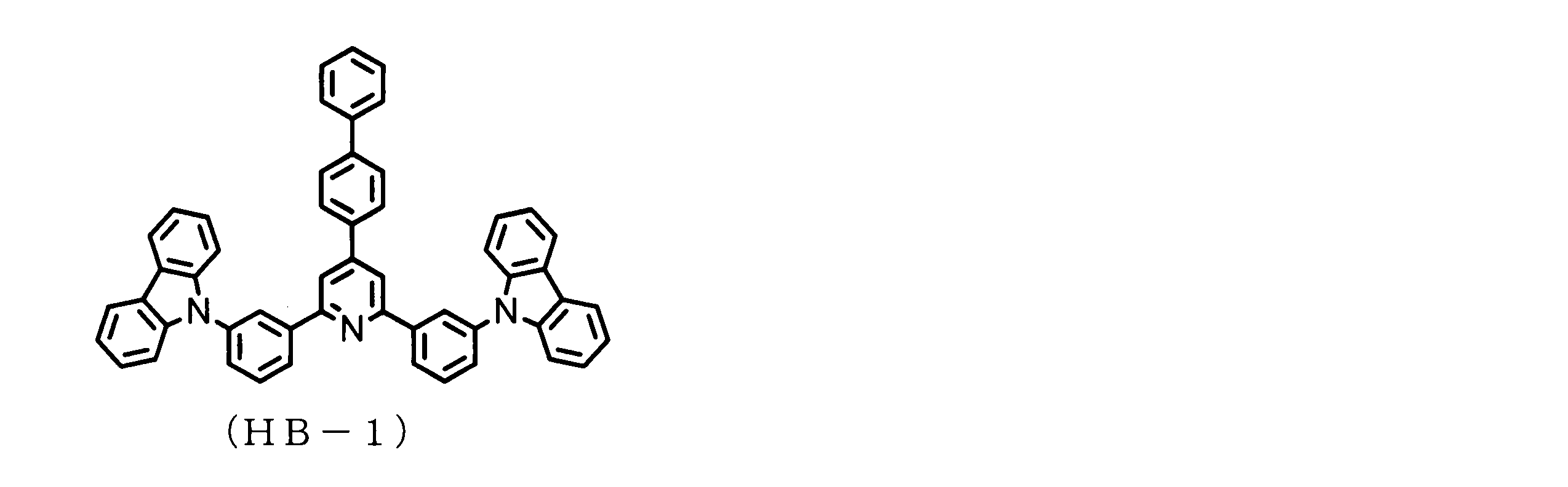
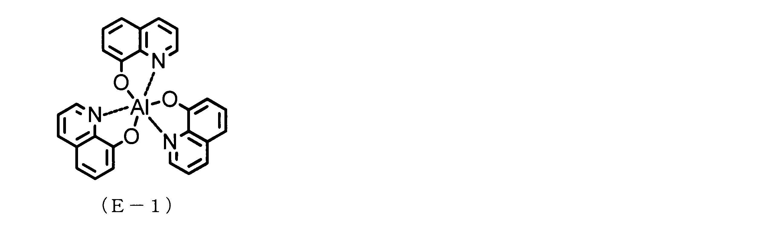
電子注入層8として、先ずフッ化リチウム(LiF)を、モリブデンボートを用いて、蒸着速度0.1~0.4Å/秒で、0.5nmの膜厚で電子輸送層7の上に形成した。次に、陰極9として、アルミニウムを同様にモリブデンボートにより加熱して、蒸着速度0.7~5.3Å/秒で、膜厚80nmのアルミニウム層を形成した。
引き続き、素子が保管中に大気中の水分等で劣化することを防ぐため、以下の方法で封止処理を行った。窒素グローブボックス中で、23mm×23mmサイズのガラス板の外周部に、1mmの幅で光硬化性樹脂(株式会社スリーボンド製30Y-437)を塗布し、中央部に水分ゲッターシート(ダイニック株式会社製)を設置した。この上に、陰極まで形成した基板を蒸着面が乾燥剤シートと対向するように貼り合わせた。その後、光硬化性樹脂が塗布された領域のみに紫外光を照射し、樹脂を硬化させた。
以上の様にして、2mm×2mmのサイズの発光面積部分を有する有機電界発光素子が得られた。この素子の特性を下記表2に示す。
発光層5として、化合物(C-1)の代わりに、化合物(C-2)、(C-4)、(C-5)をそれぞれ用いた以外は、実施例12と同様にして、有機電界発光素子を作製した。得られた素子の特性を下記表2に示す。
発光層5として、化合物(C-1)の代わりに、化合物(H-2)を用いた以外は、実施例12と同様にして、有機電界発光素子を作製した。得られた素子の特性を下記表2に示す。なお、化合物(H-2)は、ピリジン骨格であるため、本発明の範囲外となる。
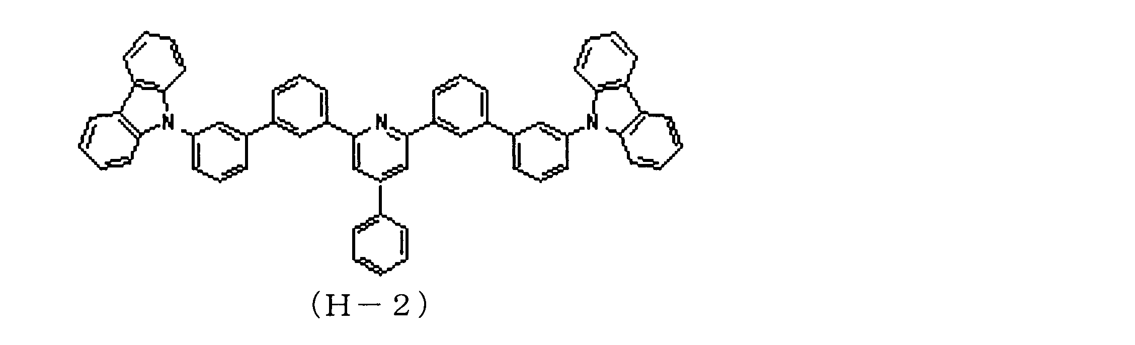

駆動寿命の測定方法は、作成した有機EL素子に、試験時直流一定電流(20mA/cm2)の電流を通電したときの輝度変化をフォトダイオードにより、観察することにより行い、輝度値が試験開始時の80%となるまでの時間を求めた。このとき、比較例2の駆動寿命を1とした時の相対的な駆動寿命を記載した。
発光層5として、化合物(C-1)、(H-1)、(D-1)の代わりに、それぞれ、化合物(C-4)、(H-3)、(D-2)を用いたほかは、実施例12と同様にして有機電界発光素子を作製した。得られた素子の特性を下記表3に示す。なお、化合物(H-3)は、日本国特開2011-26237号公報に示す方法にて合成し、化合物(D-2)は、以下に示す方法により合成した。
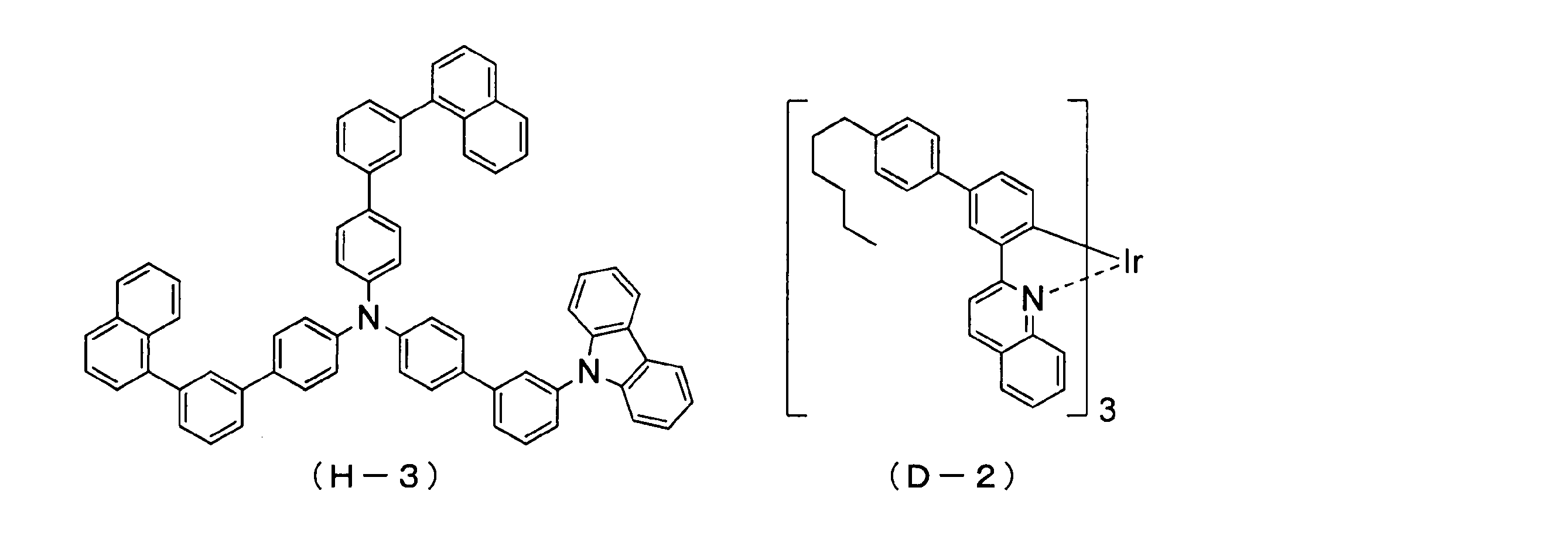
(中間体39の合成)

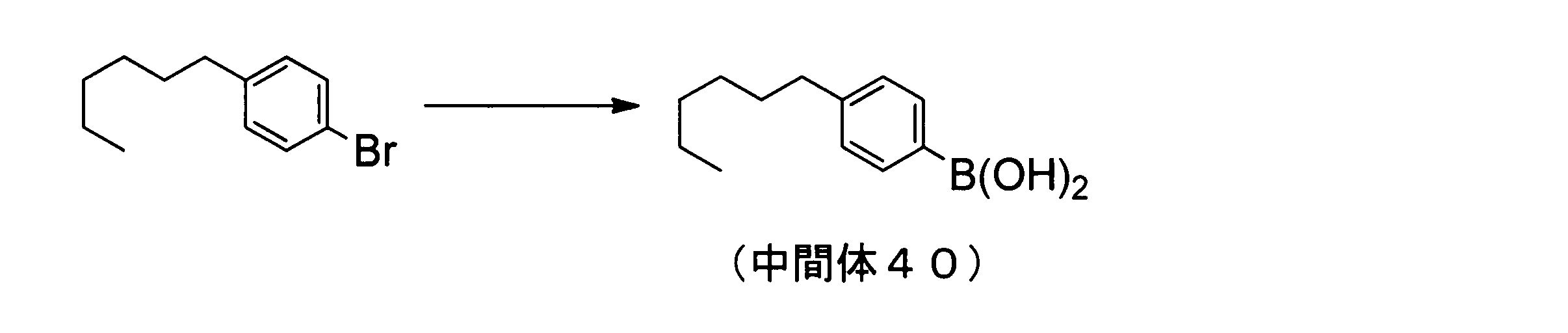
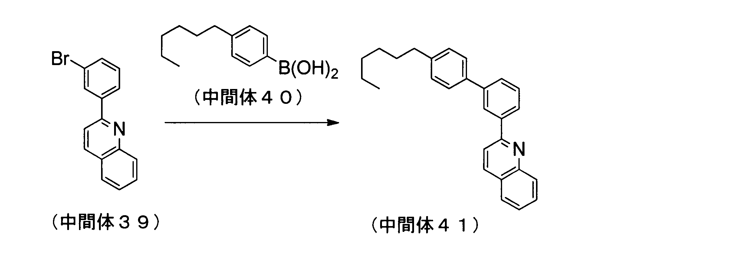
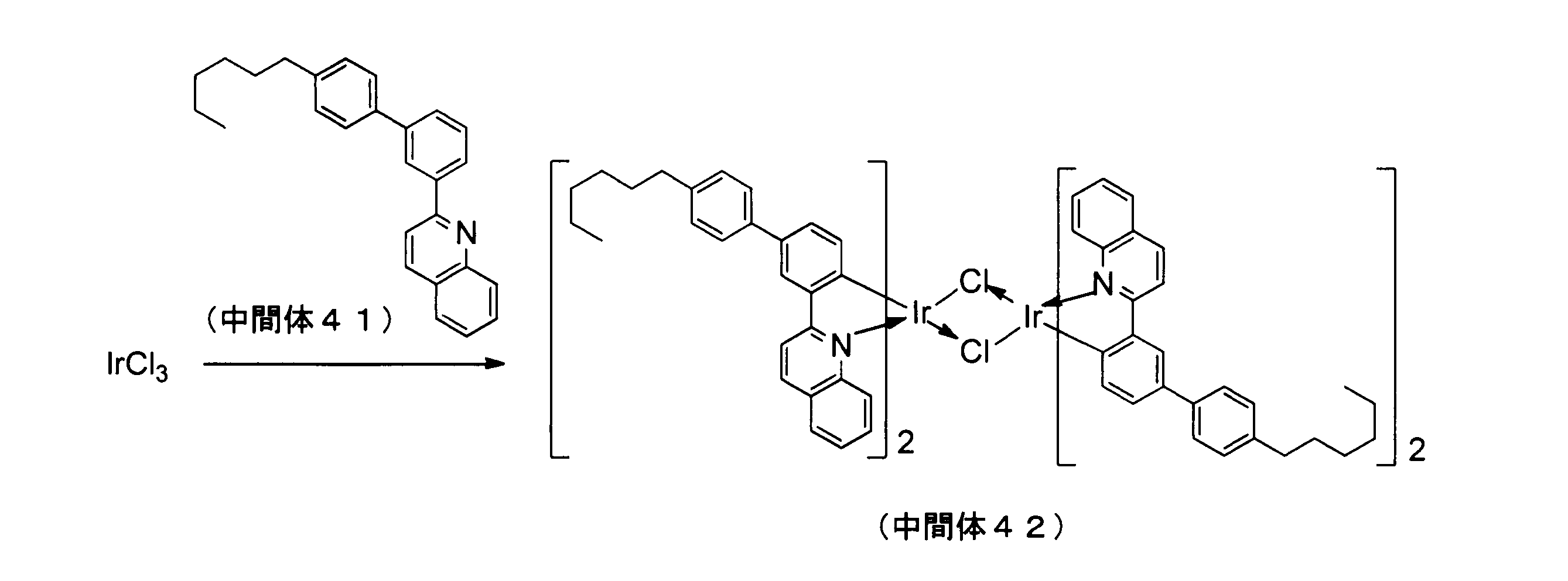
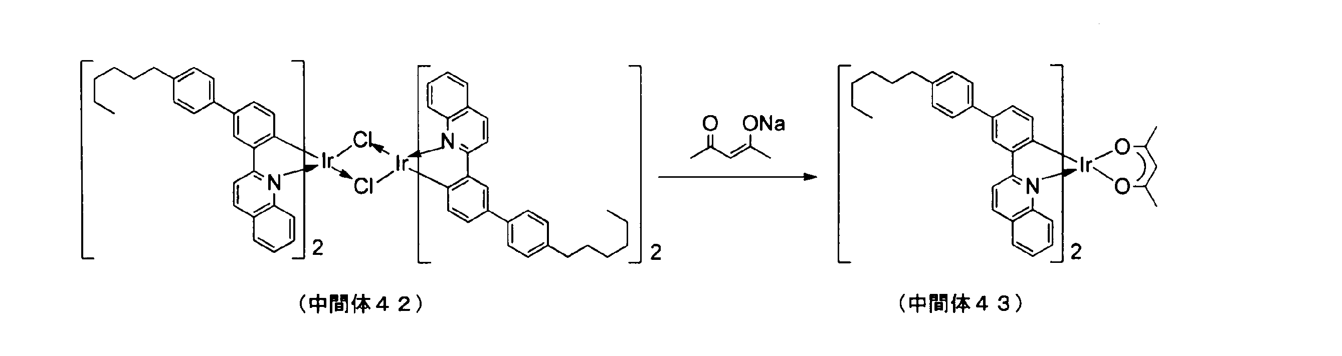
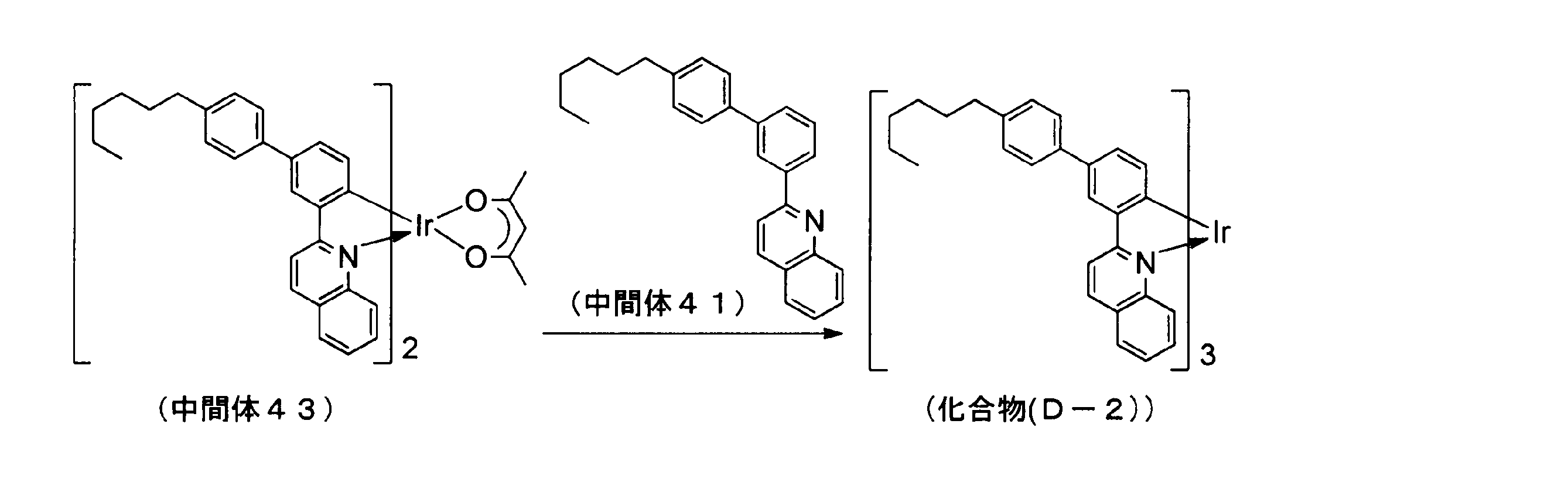
1H NMR:δ[ppm] 8.18(d、3H)、8.09(d、3H)、8.07(d、3H)、7.97(s、3H)7.67(d、3H)、7.47(d、6H)、7.20(t、3H)、7.16(d、6H)、6.96(d、3H)、6.72(t、3H)、6.61(d、3H)、2.59(t、6H)、1.30(m、24H)、0.89(t、9H).
発光層5として、化合物(C-4)の代わりに、それぞれ、化合物(C-8)、(C-9)、(C-10)、(C-11)を用いた以外は、実施例16と同様にして、有機電界発光素子を作製した。得られた素子の特性を下記表3に示す。
発光層5として、化合物(C-4)の代わりに、化合物(H-4)を用いた以外は、実施例16と同様にして、有機電界発光素子を作製した。得られた素子の特性を下記表3に示す。なお、化合物(H-4)は、分子中にカルバゾリル基を2つ有していることから本発明の範囲外となる。
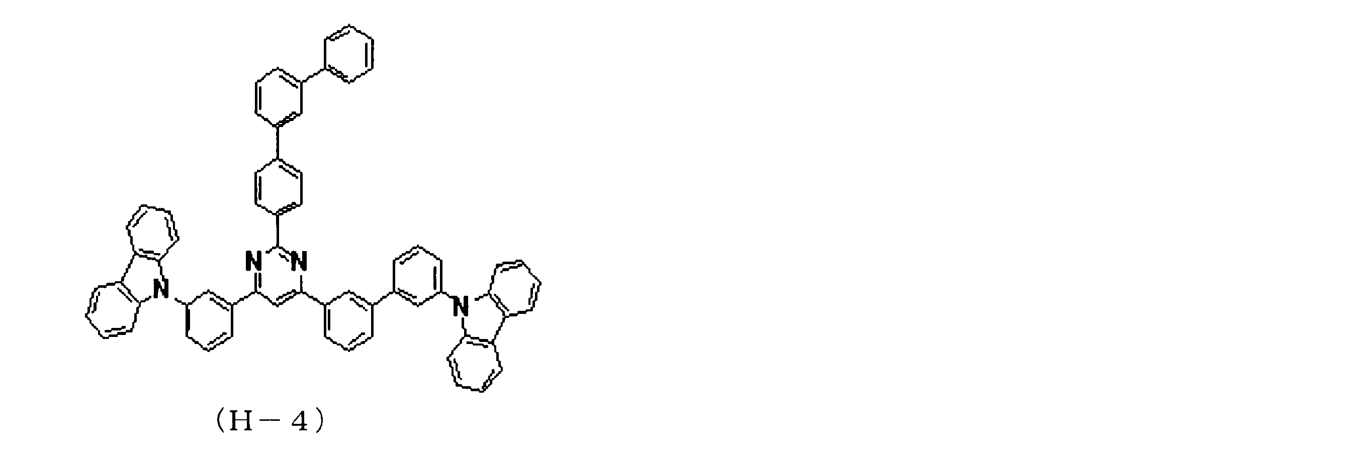
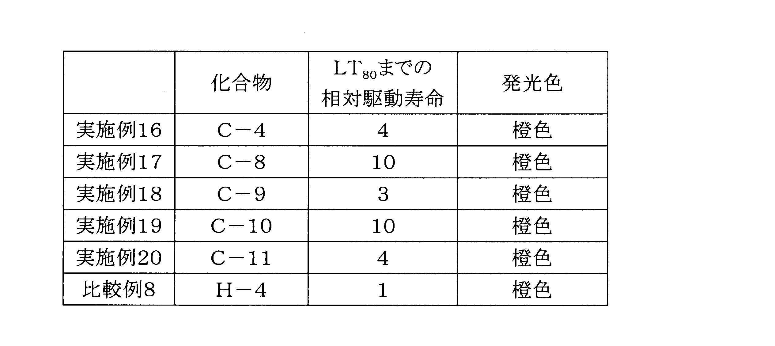
駆動寿命の測定方法は、作成した有機EL素子に、試験時直流一定電流(30mA/cm2)の電流を通電したときの輝度変化をフォトダイオードにより、観察することにより行い、輝度値が試験開始時の80%となるまでの時間を求めた。このとき、比較例1の駆動寿命を1とした時の相対的な駆動寿命を記載した。
本出願は2011年4月7日出願の日本特許出願(特願2011-085501号)に基づくものであり、その内容はここに参照として取り込まれる。
2 陽極
3 正孔注入層
4 正孔輸送層
5 発光層
6 正孔阻止層
7 電子輸送層
8 電子注入層
9 陰極
Claims (13)
- 下記一般式(1)で表され、分子量が750以上2000以下であって、分子中に存在するカルバゾリル基の数が1または0である有機化合物。
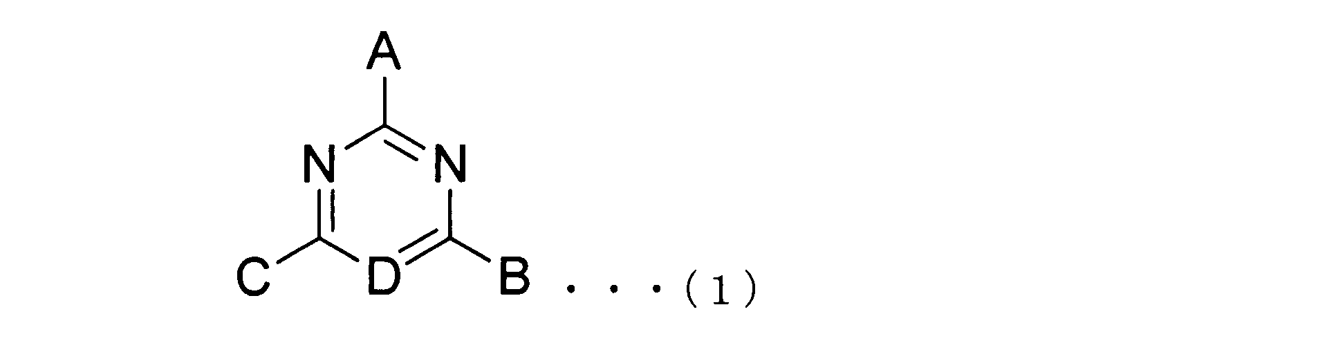
A、B、及びCは、それぞれ独立に、下記一般式(2-1)~(2-5)で表される置換基のうち、いずれかから選ばれる。
-Ar1-X1 ・・・(2-1)
-Ar2-Ar3-X2 ・・・(2-2)
-Ar4-Ar5-Ar6-X3 ・・・(2-3)
-Ar7-Ar8-Ar9-Ar10-X4・・・(2-4)
-Ar11-Ar12-Ar13-Ar14-Ar15-X5・・・(2-5)
上記一般式(2-1)~(2-5)において、Ar1は、置換基を有していてもよい1,2-フェニレン基または1,3-フェニレン基を表し、Ar2~Ar15は、それぞれ独立に、置換基を有していてもよい1,2-フェニレン基、1,3-フェニレン基または1,4-フェニレン基を表す。
X1は、置換基を有していてもよい炭素数10以上の芳香族炭化水素基、または置換基を有していてもよいカルバゾリル基を表し、X2~X5は、それぞれ独立に、置換基を有していてもよい芳香族炭化水素基、置換基を有していてもよいカルバゾリル基、置換基を有していてもよいジベンゾフラニル基、または置換基を有していてもよいジベンゾチオフェニル基を表す。
ただし、A、BおよびCは、いずれにおいても、1,2-フェニレン基及び1,3-フェニレン基のうち少なくとも1つを含み、A、B及びCは同時に同一の基を表すことはない。
Dは、CHまたは窒素原子を表す。] - 前記一般式(2-2)~(2-5)において、Ar2~Ar15が表す置換基が、それぞれ独立に、1,3-フェニレン基または1,4-フェニレン基である、請求項1に記載の有機化合物。
- 前記一般式(2-1)~(2-5)において、Ar1、Ar3、Ar6、Ar10、及びAr15が表す置換基が1,3-フェニレン基である、請求項1または2に記載の有機化合物。
- 前記一般式(1)において、A、B及びCが互いに異なる置換基である、請求項1~3のいずれか一項に記載の有機化合物。
- 下記一般式(3)で表され、分子量750以上2000以下であって、分子中に存在するカルバゾリル基の数が1または0である有機化合物。
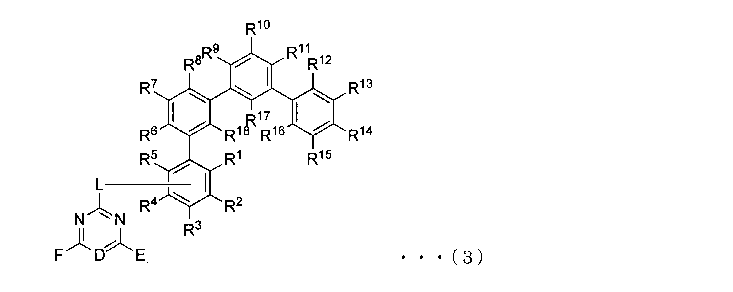
Dは、CHまたは窒素原子を表す。
E及びFは、それぞれ独立に、下記一般式(4-1)~(4-6)で表される置換基のうち、いずれかから選ばれる。
-X6 ・・・(4-1)
-Ar16-X7 ・・・(4-2)
-Ar17-Ar18-X8 ・・・(4-3)
-Ar19-Ar20-Ar21-X9 ・・・(4-4)
-Ar22-Ar23-Ar24-Ar25-X10・・・(4-5)
-Ar26-Ar27-Ar28-Ar29-Ar30-X11・・・(4-6)
上記一般式(4-1)~(4-6)において、Ar16は、置換基を有していてもよい1,2-フェニレン基または1,3-フェニレン基を表し、Ar17~Ar30は、それぞれ独立に、置換基を有していてもよい1,2-フェニレン基、1,3-フェニレン基または1,4-フェニレン基を表す。
X6~X11は、それぞれ独立に、置換基を有していてもよい芳香族炭化水素基、置換基を有していてもよいカルバゾリル基、置換基を有していてもよいジベンゾフラニル基、または置換基を有していてもよいジベンゾチエニル基を表す。
ただし、E、Fは、いずれにおいても、1,2-フェニレン基及び1,3-フェニレン基のうち少なくとも1つを含む。
Lは、直接結合、または、置換基を有していてもよい2価の芳香族炭化水素基を表し、R1~R5のいずれかの1つの置換位置との間で結合を形成する。
R1~R5は、それぞれ独立に、Lとの間での結合、水素原子、置換基を有していてもよいフェニル基、置換基を有していてもよいジベンゾフラニル基、置換基を有していてもよいジベンゾチエニル基、アルキル基、シリル基、フッ素原子、またはパーフルオロアルキル基を表し、R6~R18は、水素原子、置換基を有していてもよいフェニル基、置換基を有していてもよいジベンゾフラニル基、置換基を有していてもよいジベンゾチエニル基、アルキル基、シリル基、フッ素原子、またはパーフルオロアルキル基を表す。] - 前記一般式(4-3)~(4-6)において、Ar17~Ar30が表す置換基が、それぞれ独立に、1,3-フェニレン基または1,4-フェニレン基である、請求項5に記載の有機化合物。
- 前記一般式(4-2)~(4-6)において、Ar16、Ar18、Ar21、Ar25、及びAr30が表す置換基が1,3-フェニレン基である、請求項5または6に記載の有機化合物。
- 請求項1~7のいずれか一項に記載の有機化合物を含有する電荷輸送材料。
- 請求項1~7のいずれか一項に記載の有機化合物及び溶剤を含有する組成物。
- 陽極、陰極、及び該陽極と陰極との間に少なくとも1層の有機層を有する有機電界発光素子であり、該有機層のうち少なくとも1層が、請求項9に記載の組成物を用いて形成された層である、有機電界発光素子。
- 請求項9に記載の組成物を用いて形成された層が発光層である、請求項10に記載の有機電界発光素子。
- 請求項10または11に記載の有機電界発光素子を有する表示装置。
- 請求項10または11に記載の有機電界発光素子を有する照明装置。
Priority Applications (6)
| Application Number | Priority Date | Filing Date | Title |
|---|---|---|---|
| CN201280016418.0A CN103459375B (zh) | 2011-04-07 | 2012-04-06 | 有机化合物、电荷传输材料、含有该化合物的组合物、有机场致发光元件、显示装置及照明装置 |
| KR1020137026223A KR101813865B1 (ko) | 2011-04-07 | 2012-04-06 | 유기 화합물, 전하 수송 재료, 그 화합물을 함유하는 조성물, 유기 전계 발광 소자, 표시 장치 및 조명 장치 |
| EP12768300.1A EP2695882B1 (en) | 2011-04-07 | 2012-04-06 | Organic compound, charge transport material, composition containing said compound, organic electroluminescent element, display device, and lighting device |
| JP2012536118A JP5206907B2 (ja) | 2011-04-07 | 2012-04-06 | 有機化合物、電荷輸送材料、該化合物を含有する組成物、有機電界発光素子、表示装置及び照明装置 |
| US14/047,403 US8945728B2 (en) | 2011-04-07 | 2013-10-07 | Organic compound, charge-transporting material, composition containing the compound, organic electroluminescent element, display device, and lighting device |
| US14/547,614 US9564602B2 (en) | 2011-04-07 | 2014-11-19 | Organic compound, charge-transporting material, composition containing the compound, organic electroluminescent element, display device, and lighting device |
Applications Claiming Priority (2)
| Application Number | Priority Date | Filing Date | Title |
|---|---|---|---|
| JP2011085501 | 2011-04-07 | ||
| JP2011-085501 | 2011-04-07 |
Related Child Applications (1)
| Application Number | Title | Priority Date | Filing Date |
|---|---|---|---|
| US14/047,403 Continuation US8945728B2 (en) | 2011-04-07 | 2013-10-07 | Organic compound, charge-transporting material, composition containing the compound, organic electroluminescent element, display device, and lighting device |
Publications (1)
| Publication Number | Publication Date |
|---|---|
| WO2012137958A1 true WO2012137958A1 (ja) | 2012-10-11 |
Family
ID=46969346
Family Applications (1)
| Application Number | Title | Priority Date | Filing Date |
|---|---|---|---|
| PCT/JP2012/059600 Ceased WO2012137958A1 (ja) | 2011-04-07 | 2012-04-06 | 有機化合物、電荷輸送材料、該化合物を含有する組成物、有機電界発光素子、表示装置及び照明装置 |
Country Status (7)
| Country | Link |
|---|---|
| US (2) | US8945728B2 (ja) |
| EP (1) | EP2695882B1 (ja) |
| JP (1) | JP5206907B2 (ja) |
| KR (1) | KR101813865B1 (ja) |
| CN (2) | CN106632112B (ja) |
| TW (1) | TWI557116B (ja) |
| WO (1) | WO2012137958A1 (ja) |
Cited By (27)
| Publication number | Priority date | Publication date | Assignee | Title |
|---|---|---|---|---|
| WO2015008866A1 (ja) * | 2013-07-19 | 2015-01-22 | 東ソー株式会社 | トリアジン化合物及びそれを含有する有機電界発光素子 |
| US20150214489A1 (en) * | 2012-07-23 | 2015-07-30 | Merck Patent Gmbh | Materials for organic electroluminescent devices |
| JP2016019002A (ja) * | 2014-07-09 | 2016-02-01 | ユニバーサル ディスプレイ コーポレイション | 有機エレクトロルミネッセンス材料及びデバイス |
| KR20160126698A (ko) * | 2015-04-24 | 2016-11-02 | 삼성에스디아이 주식회사 | 유기 광전자 소자용 화합물, 유기 광전자 소자 및 표시장치 |
| US20170222158A1 (en) * | 2014-10-31 | 2017-08-03 | Samsung Sdi Co., Ltd. | Organic optoelectronic device and display device |
| JP2017155003A (ja) * | 2016-03-02 | 2017-09-07 | 株式会社Kyulux | 化合物、キャリア輸送材料および有機発光素子 |
| JP2017160144A (ja) * | 2016-03-08 | 2017-09-14 | 東ソー株式会社 | 4,6−ジクロロトリアジン化合物及びその製造方法 |
| JP2017160145A (ja) * | 2016-03-08 | 2017-09-14 | 東ソー株式会社 | トリアリールトリアジン化合物の製造方法 |
| WO2018074507A1 (ja) * | 2016-10-19 | 2018-04-26 | 積水化学工業株式会社 | 有機el表示素子用封止剤及び有機el表示素子用封止剤の製造方法 |
| WO2018074508A1 (ja) * | 2016-10-19 | 2018-04-26 | 積水化学工業株式会社 | 有機el表示素子用封止剤 |
| US10147891B2 (en) | 2014-01-09 | 2018-12-04 | Samsung Sdi Co., Ltd. | Organic compound, organic optoelectronic device, and display device |
| US10158085B2 (en) | 2013-12-17 | 2018-12-18 | Samsung Electronics Co., Ltd. | Condensed cyclic compound and organic light-emitting device including the same |
| WO2019188794A1 (ja) * | 2018-03-30 | 2019-10-03 | 積水化学工業株式会社 | 有機el表示素子用封止剤 |
| JP2019172608A (ja) * | 2018-03-28 | 2019-10-10 | 三菱ケミカル株式会社 | 1,3,5−トリアジン化合物、該化合物を含有する組成物、有機電界発光素子、表示装置及び照明装置 |
| US10446764B2 (en) | 2014-05-22 | 2019-10-15 | Samsung Sdi Co., Ltd. | Organic compound, composition, organic optoelectric device, and display device |
| JPWO2018135656A1 (ja) * | 2017-01-23 | 2019-11-07 | 三菱ケミカル株式会社 | 発光層形成用組成物及び該発光層形成用組成物を含有する有機電界発光素子 |
| JP2020088398A (ja) * | 2018-11-28 | 2020-06-04 | 三星エスディアイ株式会社Samsung SDI Co., Ltd. | 有機光電子素子用化合物、有機光電子素子、および表示装置 |
| US10784447B2 (en) | 2015-04-24 | 2020-09-22 | Samsung Sdi Co., Ltd. | Organic compound, composition, and organic optoelectronic diode |
| JPWO2020251031A1 (ja) * | 2019-06-13 | 2020-12-17 | ||
| US10873033B2 (en) | 2014-04-09 | 2020-12-22 | Samsung Sdi Co., Ltd. | Organic compound, composition, organic optoelectronic diode, and display device |
| US10985329B2 (en) | 2013-12-17 | 2021-04-20 | Samsung Electronics Co., Ltd. | Condensed cyclic compound and organic light-emitting device including the same |
| US11177441B2 (en) | 2014-01-24 | 2021-11-16 | Samsung Sdi Co., Ltd. | Organic compound, composition, organic optoelectronic device, and display device |
| JPWO2022255403A1 (ja) * | 2021-06-04 | 2022-12-08 | ||
| WO2022255428A1 (ja) * | 2021-06-04 | 2022-12-08 | 三菱ケミカル株式会社 | 芳香族化合物、有機電界発光素子、組成物及び有機電界発光素子の製造方法 |
| JP2023086108A (ja) * | 2021-12-09 | 2023-06-21 | 三菱ケミカル株式会社 | 化合物及び有機電界発光素子 |
| WO2023181737A1 (ja) * | 2022-03-25 | 2023-09-28 | 住友化学株式会社 | 組成物及びそれを用いた発光素子の製造方法 |
| WO2023181507A1 (ja) * | 2022-03-25 | 2023-09-28 | 三菱ケミカル株式会社 | 有機電界発光素子の発光層用材料、発光層形成用組成物、有機電界発光素子、及び有機電界発光素子の製造方法 |
Families Citing this family (24)
| Publication number | Priority date | Publication date | Assignee | Title |
|---|---|---|---|---|
| US9847501B2 (en) * | 2011-11-22 | 2017-12-19 | Idemitsu Kosan Co., Ltd. | Aromatic heterocyclic derivative, material for organic electroluminescent element, and organic electroluminescent element |
| US9231217B2 (en) * | 2013-11-28 | 2016-01-05 | Semiconductor Energy Laboratory Co., Ltd. | Synthesis method of organometallic complex, synthesis method of pyrazine derivative, 5,6-diaryl-2-pyrazyl triflate, light-emitting element, light-emitting device, electronic device, and lighting device |
| KR101857146B1 (ko) * | 2014-10-28 | 2018-05-11 | 삼성에스디아이 주식회사 | 유기 광전자 소자 및 표시 장치 |
| KR101848347B1 (ko) * | 2014-10-28 | 2018-05-24 | 삼성에스디아이 주식회사 | 유기 광전자 소자 및 표시 장치 |
| KR101903929B1 (ko) * | 2015-04-24 | 2018-10-02 | 스미또모 가가꾸 가부시키가이샤 | 발광 소자 및 해당 발광 소자에 사용하는 조성물 |
| KR101958833B1 (ko) * | 2015-09-21 | 2019-03-15 | 삼성에스디아이 주식회사 | 유기 광전자 소자 및 표시 장치 |
| KR101940169B1 (ko) | 2016-02-04 | 2019-01-18 | 삼성에스디아이 주식회사 | 유기 광전자 소자용 화합물, 유기 광전자 소자 및 표시 장치 |
| KR102044942B1 (ko) | 2016-05-02 | 2019-11-14 | 삼성에스디아이 주식회사 | 유기 광전자 소자용 화합물, 유기 광전자 소자 및 표시 장치 |
| KR102054276B1 (ko) | 2016-06-29 | 2019-12-10 | 삼성에스디아이 주식회사 | 유기 광전자 소자용 화합물, 유기 광전자 소자용 조성물, 유기 광전자 소자 및 표시 장치 |
| KR102027961B1 (ko) | 2016-06-29 | 2019-10-02 | 삼성에스디아이 주식회사 | 유기 광전자 소자용 화합물, 유기 광전자 소자용 조성물, 유기 광전자 소자 및 표시 장치 |
| KR102050000B1 (ko) | 2016-07-12 | 2019-11-28 | 삼성에스디아이 주식회사 | 유기 광전자 소자용 화합물, 유기 광전자 소자용 조성물, 유기 광전자 소자 및 표시 장치 |
| KR102054277B1 (ko) | 2016-07-29 | 2019-12-10 | 삼성에스디아이 주식회사 | 유기 광전자 소자용 조성물, 유기 광전자 소자 및 표시 장치 |
| KR102199076B1 (ko) | 2017-01-05 | 2021-01-07 | 삼성에스디아이 주식회사 | 유기 광전자 소자용 화합물, 유기 광전자 소자용 조성물, 유기 광전자 소자 및 표시 장치 |
| KR102008897B1 (ko) | 2017-06-22 | 2019-10-23 | 삼성에스디아이 주식회사 | 유기 광전자 소자 및 표시 장치 |
| US20190198772A1 (en) | 2017-06-22 | 2019-06-27 | Samsung Sdi Co., Ltd. | Compound for organic optoelectronic device, composition for organic optoelectronic device and organic optoelectronic device and display deivce |
| KR101947747B1 (ko) | 2018-05-04 | 2019-02-13 | 삼성에스디아이 주식회사 | 유기 광전자 소자용 화합물, 유기 광전자 소자용 조성물, 유기 광전자 소자 및 표시 장치 |
| CN108346750B (zh) * | 2017-08-08 | 2019-07-19 | 广东聚华印刷显示技术有限公司 | 电致发光器件及其发光层和应用 |
| CN109535138B (zh) * | 2017-09-22 | 2021-03-12 | 北京绿人科技有限责任公司 | 含氘代苯基的三嗪化合物及其应用和有机电致发光器件 |
| TWI787355B (zh) * | 2017-09-22 | 2022-12-21 | 日商三菱化學股份有限公司 | 電荷輸送性化合物、包含電荷輸送性化合物的組成物、有機電場發光元件、有機電場發光顯示裝置、有機電場發光照明 |
| CN108424411A (zh) * | 2017-09-30 | 2018-08-21 | 北京绿人科技有限责任公司 | 具有对称结构的三嗪化合物及其应用和有机电致发光器件 |
| JP7199868B2 (ja) | 2017-10-10 | 2023-01-06 | キヤノン株式会社 | エレクトロクロミック素子、光学フィルタ、レンズユニット、撮像装置、および、窓材 |
| CN107827826A (zh) * | 2017-11-02 | 2018-03-23 | 上海道亦化工科技有限公司 | 一种嘧啶衍生物及其用途和有机电致发光器件 |
| KR101857632B1 (ko) * | 2018-02-02 | 2018-05-14 | 덕산네오룩스 주식회사 | 유기전기소자용 화합물, 이를 이용한 유기전기소자 및 그 전자 장치 |
| KR102869108B1 (ko) * | 2019-10-24 | 2025-10-14 | 듀폰스페셜티머터리얼스코리아 유한회사 | 복수 종의 호스트 재료 및 이를 포함하는 유기 전계 발광 소자 |
Citations (31)
| Publication number | Priority date | Publication date | Assignee | Title |
|---|---|---|---|---|
| JPS59194393A (ja) | 1983-03-25 | 1984-11-05 | イ−ストマン コダツク カンパニ− | 改良された電力転換効率をもつ有機エレクトロルミネツセント装置 |
| JPH05331459A (ja) | 1992-04-03 | 1993-12-14 | Pioneer Electron Corp | 有機エレクトロルミネッセンス素子 |
| JPH06207169A (ja) | 1992-11-17 | 1994-07-26 | Idemitsu Kosan Co Ltd | 有機エレクトロルミネッセンス素子 |
| JPH0741759A (ja) | 1993-03-26 | 1995-02-10 | Sumitomo Electric Ind Ltd | 有機エレクトロルミネッセンス素子 |
| US5645948A (en) | 1996-08-20 | 1997-07-08 | Eastman Kodak Company | Blue organic electroluminescent devices |
| JPH1074586A (ja) | 1996-07-29 | 1998-03-17 | Eastman Kodak Co | エレクトロルミネセンスデバイスで用いられる二層電子注入電極 |
| JPH1079297A (ja) | 1996-07-09 | 1998-03-24 | Sony Corp | 電界発光素子 |
| JPH10270171A (ja) | 1997-01-27 | 1998-10-09 | Junji Kido | 有機エレクトロルミネッセント素子 |
| JPH11242996A (ja) | 1998-02-25 | 1999-09-07 | Mitsubishi Chemical Corp | 有機電界発光素子 |
| JPH11251067A (ja) | 1998-03-02 | 1999-09-17 | Junji Kido | 有機エレクトロルミネッセント素子 |
| US6225467B1 (en) | 2000-01-21 | 2001-05-01 | Xerox Corporation | Electroluminescent (EL) devices |
| JP2002100482A (ja) | 2000-09-20 | 2002-04-05 | Mitsubishi Chemicals Corp | 有機電界発光素子 |
| JP2002100478A (ja) | 2000-09-20 | 2002-04-05 | Mitsubishi Chemicals Corp | 有機電界発光素子及びその製造方法 |
| JP2003031365A (ja) | 2001-05-02 | 2003-01-31 | Junji Kido | 有機電界発光素子 |
| JP2004022334A (ja) | 2002-06-17 | 2004-01-22 | Konica Minolta Holdings Inc | 有機エレクトロルミネッセンス素子及び表示装置 |
| JP2004031004A (ja) | 2002-06-24 | 2004-01-29 | Konica Minolta Holdings Inc | 有機エレクトロルミネッセンス素子及び表示装置 |
| WO2004039786A1 (en) * | 2002-10-30 | 2004-05-13 | Ciba Specialty Chemicals Holding Inc. | Electroluminescent device |
| WO2004084260A2 (en) | 2003-03-20 | 2004-09-30 | Cambridge Display Technology Limited | Electroluminescent device |
| WO2005022962A1 (ja) | 2003-07-31 | 2005-03-10 | Mitsubishi Chemical Corporation | 化合物、電荷輸送材料および有機電界発光素子 |
| WO2005089024A1 (ja) | 2004-03-11 | 2005-09-22 | Mitsubishi Chemical Corporation | 電荷輸送膜用組成物及びイオン化合物、それを用いた電荷輸送膜及び有機電界発光素子、並びに、有機電界発光素子の製造方法及び電荷輸送膜の製造方法 |
| WO2006062062A1 (ja) | 2004-12-10 | 2006-06-15 | Pioneer Corporation | 有機化合物、電荷輸送材料および有機電界発光素子 |
| JP2006190759A (ja) | 2005-01-05 | 2006-07-20 | Idemitsu Kosan Co Ltd | 有機エレクトロルミネッセンス素子 |
| JP2006188493A (ja) | 2004-12-10 | 2006-07-20 | Pioneer Electronic Corp | 有機化合物、電荷輸送材料および有機電界発光素子 |
| JP2008098619A (ja) | 2006-09-14 | 2008-04-24 | Sumitomo Chemical Co Ltd | 有機エレクトロルミネッセンス素子 |
| JP4474493B1 (ja) | 2009-07-31 | 2010-06-02 | 富士フイルム株式会社 | 有機電界発光素子 |
| JP2010206191A (ja) | 2009-02-09 | 2010-09-16 | Mitsubishi Chemicals Corp | 有機電界発光素子材料、湿式成膜用有機電界発光素子用組成物および有機電界発光素子 |
| JP2010202644A (ja) | 2009-02-03 | 2010-09-16 | Mitsubishi Chemicals Corp | 有機金属錯体、有機金属錯体含有組成物、発光材料、有機電界発光素子材料、有機電界発光素子、有機elディスプレイおよび有機el照明 |
| JP2010278287A (ja) | 2009-05-29 | 2010-12-09 | Konica Minolta Holdings Inc | 有機エレクトロルミネッセンス素子、該素子を用いた表示装置、照明装置及び有機エレクトロルミネッセンス素子の製造方法 |
| JP2011026237A (ja) | 2009-07-24 | 2011-02-10 | Mitsubishi Chemicals Corp | 有機化合物、電荷輸送材料、有機電界発光素子用組成物、有機電界発光素子、有機elディスプレイ及び有機el照明 |
| WO2011021689A1 (ja) * | 2009-08-21 | 2011-02-24 | 東ソー株式会社 | 環状アジン誘導体とそれらの製造方法、ならびにそれらを構成成分とする有機電界発光素子 |
| WO2011024922A1 (ja) | 2009-08-27 | 2011-03-03 | 三菱化学株式会社 | モノアミン化合物、電荷輸送材料、電荷輸送膜用組成物、有機電界発光素子、有機el表示装置及び有機el照明 |
Family Cites Families (5)
| Publication number | Priority date | Publication date | Assignee | Title |
|---|---|---|---|---|
| GB0225244D0 (en) * | 2002-10-30 | 2002-12-11 | Ciba Sc Holding Ag | Electroluminescent device |
| ES2435512T3 (es) * | 2003-03-24 | 2013-12-20 | Basf Se | Derivados simétricos de triazina |
| KR100730140B1 (ko) * | 2005-07-15 | 2007-06-19 | 삼성에스디아이 주식회사 | 트리아진계 화합물 및 이를 이용한 유기 발광 소자 |
| KR101395615B1 (ko) * | 2005-11-30 | 2014-05-16 | 미쓰비시 가가꾸 가부시키가이샤 | 유기 화합물, 전하 수송 재료, 전하 수송 재료용 조성물 및유기 전계 발광 소자 |
| EP2463930B1 (en) * | 2006-01-05 | 2017-04-12 | Konica Minolta Holdings, Inc. | Organic electroluminescent device, display and illuminating device |
-
2012
- 2012-04-06 JP JP2012536118A patent/JP5206907B2/ja active Active
- 2012-04-06 TW TW101112413A patent/TWI557116B/zh active
- 2012-04-06 WO PCT/JP2012/059600 patent/WO2012137958A1/ja not_active Ceased
- 2012-04-06 CN CN201610730855.9A patent/CN106632112B/zh active Active
- 2012-04-06 CN CN201280016418.0A patent/CN103459375B/zh active Active
- 2012-04-06 KR KR1020137026223A patent/KR101813865B1/ko active Active
- 2012-04-06 EP EP12768300.1A patent/EP2695882B1/en active Active
-
2013
- 2013-10-07 US US14/047,403 patent/US8945728B2/en active Active
-
2014
- 2014-11-19 US US14/547,614 patent/US9564602B2/en active Active
Patent Citations (32)
| Publication number | Priority date | Publication date | Assignee | Title |
|---|---|---|---|---|
| JPS59194393A (ja) | 1983-03-25 | 1984-11-05 | イ−ストマン コダツク カンパニ− | 改良された電力転換効率をもつ有機エレクトロルミネツセント装置 |
| JPH05331459A (ja) | 1992-04-03 | 1993-12-14 | Pioneer Electron Corp | 有機エレクトロルミネッセンス素子 |
| JPH06207169A (ja) | 1992-11-17 | 1994-07-26 | Idemitsu Kosan Co Ltd | 有機エレクトロルミネッセンス素子 |
| JPH0741759A (ja) | 1993-03-26 | 1995-02-10 | Sumitomo Electric Ind Ltd | 有機エレクトロルミネッセンス素子 |
| JPH1079297A (ja) | 1996-07-09 | 1998-03-24 | Sony Corp | 電界発光素子 |
| JPH1074586A (ja) | 1996-07-29 | 1998-03-17 | Eastman Kodak Co | エレクトロルミネセンスデバイスで用いられる二層電子注入電極 |
| US5645948A (en) | 1996-08-20 | 1997-07-08 | Eastman Kodak Company | Blue organic electroluminescent devices |
| JPH10270171A (ja) | 1997-01-27 | 1998-10-09 | Junji Kido | 有機エレクトロルミネッセント素子 |
| JPH11242996A (ja) | 1998-02-25 | 1999-09-07 | Mitsubishi Chemical Corp | 有機電界発光素子 |
| JPH11251067A (ja) | 1998-03-02 | 1999-09-17 | Junji Kido | 有機エレクトロルミネッセント素子 |
| US6225467B1 (en) | 2000-01-21 | 2001-05-01 | Xerox Corporation | Electroluminescent (EL) devices |
| JP2002100482A (ja) | 2000-09-20 | 2002-04-05 | Mitsubishi Chemicals Corp | 有機電界発光素子 |
| JP2002100478A (ja) | 2000-09-20 | 2002-04-05 | Mitsubishi Chemicals Corp | 有機電界発光素子及びその製造方法 |
| JP2003031365A (ja) | 2001-05-02 | 2003-01-31 | Junji Kido | 有機電界発光素子 |
| JP2004022334A (ja) | 2002-06-17 | 2004-01-22 | Konica Minolta Holdings Inc | 有機エレクトロルミネッセンス素子及び表示装置 |
| JP2004031004A (ja) | 2002-06-24 | 2004-01-29 | Konica Minolta Holdings Inc | 有機エレクトロルミネッセンス素子及び表示装置 |
| WO2004039786A1 (en) * | 2002-10-30 | 2004-05-13 | Ciba Specialty Chemicals Holding Inc. | Electroluminescent device |
| WO2004084260A2 (en) | 2003-03-20 | 2004-09-30 | Cambridge Display Technology Limited | Electroluminescent device |
| WO2005022962A1 (ja) | 2003-07-31 | 2005-03-10 | Mitsubishi Chemical Corporation | 化合物、電荷輸送材料および有機電界発光素子 |
| WO2005089024A1 (ja) | 2004-03-11 | 2005-09-22 | Mitsubishi Chemical Corporation | 電荷輸送膜用組成物及びイオン化合物、それを用いた電荷輸送膜及び有機電界発光素子、並びに、有機電界発光素子の製造方法及び電荷輸送膜の製造方法 |
| WO2006062062A1 (ja) | 2004-12-10 | 2006-06-15 | Pioneer Corporation | 有機化合物、電荷輸送材料および有機電界発光素子 |
| JP2006188493A (ja) | 2004-12-10 | 2006-07-20 | Pioneer Electronic Corp | 有機化合物、電荷輸送材料および有機電界発光素子 |
| JP2006190759A (ja) | 2005-01-05 | 2006-07-20 | Idemitsu Kosan Co Ltd | 有機エレクトロルミネッセンス素子 |
| JP2008098619A (ja) | 2006-09-14 | 2008-04-24 | Sumitomo Chemical Co Ltd | 有機エレクトロルミネッセンス素子 |
| JP2010202644A (ja) | 2009-02-03 | 2010-09-16 | Mitsubishi Chemicals Corp | 有機金属錯体、有機金属錯体含有組成物、発光材料、有機電界発光素子材料、有機電界発光素子、有機elディスプレイおよび有機el照明 |
| JP2010206191A (ja) | 2009-02-09 | 2010-09-16 | Mitsubishi Chemicals Corp | 有機電界発光素子材料、湿式成膜用有機電界発光素子用組成物および有機電界発光素子 |
| JP2010278287A (ja) | 2009-05-29 | 2010-12-09 | Konica Minolta Holdings Inc | 有機エレクトロルミネッセンス素子、該素子を用いた表示装置、照明装置及び有機エレクトロルミネッセンス素子の製造方法 |
| JP2011026237A (ja) | 2009-07-24 | 2011-02-10 | Mitsubishi Chemicals Corp | 有機化合物、電荷輸送材料、有機電界発光素子用組成物、有機電界発光素子、有機elディスプレイ及び有機el照明 |
| JP4474493B1 (ja) | 2009-07-31 | 2010-06-02 | 富士フイルム株式会社 | 有機電界発光素子 |
| WO2011013843A1 (en) * | 2009-07-31 | 2011-02-03 | Fujifilm Corporation | Organic electroluminescence device |
| WO2011021689A1 (ja) * | 2009-08-21 | 2011-02-24 | 東ソー株式会社 | 環状アジン誘導体とそれらの製造方法、ならびにそれらを構成成分とする有機電界発光素子 |
| WO2011024922A1 (ja) | 2009-08-27 | 2011-03-03 | 三菱化学株式会社 | モノアミン化合物、電荷輸送材料、電荷輸送膜用組成物、有機電界発光素子、有機el表示装置及び有機el照明 |
Non-Patent Citations (17)
| Title |
|---|
| ADVANCED MATERIALS, vol. 22, 2010, pages 3311 - 3316 |
| APPL. PHYS. LETT., vol. 60, 1992, pages 2711 |
| APPL. PHYS. LETT., vol. 70, 1997, pages 152 |
| CHEMICAL COMMUNICATIONS, vol. 46, no. 27, 2010, pages 4902 - 4904 |
| CHEMISTRY OF MATERIALS, vol. 18, 2006, pages 204 - 213 |
| IEEE TRANS. ELECTRON. DEVICES, vol. 44, 1997, pages 1245 |
| J. ORG. CHEM., vol. 66, 2001, pages 7125 - 7128 |
| JOURNAL OF ORGANIC CHEMISTRY, vol. 67, no. 24, 2002, pages 8424 - 8429 |
| JOURNAL OFMATERIALS CHEMISTRY, vol. 19, 2009, pages 8112 - 8118 |
| KUNIEDA ET AL.: "Hetero Kan No Kagaku - Iyakuhin No Kiso", 2002, KAGAKU-DOJIN PUBLISHING COMPANY, INC. |
| ORGANIC LETTERS, vol. 10, no. 5, 2008, pages 709 - 712 |
| ORGANIC LETTERS, vol. 3, no. 15, 2001, pages 2419 - 2421 |
| See also references of EP2695882A4 |
| SID 04 DIGEST, pages 154 |
| SYNTHETIC METALS, vol. 122, no. 3, 2001, pages 485 - 493 |
| TOKITO SHIZUO; ADACHI CHIHAYA; MURATA HIDEYUKI: "Yuki EL Disupurei", 20 August 2004, OHMSHA, LTD. |
| YAMANAKA ET AL.: "Shinpen Hetero Kan Kagobutsu Kisohen, ?y?hen", 2004, KODANSHA LTD. |
Cited By (58)
| Publication number | Priority date | Publication date | Assignee | Title |
|---|---|---|---|---|
| US20150214489A1 (en) * | 2012-07-23 | 2015-07-30 | Merck Patent Gmbh | Materials for organic electroluminescent devices |
| JP2015530363A (ja) * | 2012-07-23 | 2015-10-15 | メルク パテント ゲーエムベーハー | 有機エレクトロルミネッセンス素子のための材料 |
| US12022732B2 (en) | 2012-07-23 | 2024-06-25 | Merck Patent Gmbh | Materials for organic electroluminescent devices |
| US10991892B2 (en) * | 2012-07-23 | 2021-04-27 | Merck Patent Gmbh | Materials for organic electroluminescent devices |
| WO2015008866A1 (ja) * | 2013-07-19 | 2015-01-22 | 東ソー株式会社 | トリアジン化合物及びそれを含有する有機電界発光素子 |
| US12384766B2 (en) | 2013-12-17 | 2025-08-12 | Samsung Electronics Co., Ltd. | Condensed cyclic compound and organic light-emitting device including the same |
| US12150380B2 (en) | 2013-12-17 | 2024-11-19 | Samsung Electronics Co., Ltd. | Condensed cyclic compound and organic light-emitting device including the same |
| US10985329B2 (en) | 2013-12-17 | 2021-04-20 | Samsung Electronics Co., Ltd. | Condensed cyclic compound and organic light-emitting device including the same |
| US10158085B2 (en) | 2013-12-17 | 2018-12-18 | Samsung Electronics Co., Ltd. | Condensed cyclic compound and organic light-emitting device including the same |
| US10147891B2 (en) | 2014-01-09 | 2018-12-04 | Samsung Sdi Co., Ltd. | Organic compound, organic optoelectronic device, and display device |
| US11177441B2 (en) | 2014-01-24 | 2021-11-16 | Samsung Sdi Co., Ltd. | Organic compound, composition, organic optoelectronic device, and display device |
| US10873033B2 (en) | 2014-04-09 | 2020-12-22 | Samsung Sdi Co., Ltd. | Organic compound, composition, organic optoelectronic diode, and display device |
| US10446764B2 (en) | 2014-05-22 | 2019-10-15 | Samsung Sdi Co., Ltd. | Organic compound, composition, organic optoelectric device, and display device |
| JP2023156280A (ja) * | 2014-07-09 | 2023-10-24 | ユニバーサル ディスプレイ コーポレイション | 有機エレクトロルミネッセンス材料及びデバイス |
| JP7663794B2 (ja) | 2014-07-09 | 2025-04-17 | ユニバーサル ディスプレイ コーポレイション | 有機エレクトロルミネッセンス材料及びデバイス |
| JP2022091758A (ja) * | 2014-07-09 | 2022-06-21 | ユニバーサル ディスプレイ コーポレイション | 有機エレクトロルミネッセンス材料及びデバイス |
| JP7313500B2 (ja) | 2014-07-09 | 2023-07-24 | ユニバーサル ディスプレイ コーポレイション | 有機エレクトロルミネッセンス材料及びデバイス |
| JP2016019002A (ja) * | 2014-07-09 | 2016-02-01 | ユニバーサル ディスプレイ コーポレイション | 有機エレクトロルミネッセンス材料及びデバイス |
| US11145820B2 (en) * | 2014-10-31 | 2021-10-12 | Samsung Sdi Co., Ltd. | Organic optoelectronic device and display device |
| US20170222158A1 (en) * | 2014-10-31 | 2017-08-03 | Samsung Sdi Co., Ltd. | Organic optoelectronic device and display device |
| US10797245B2 (en) | 2015-04-24 | 2020-10-06 | Samsung Sdi Co., Ltd. | Compound for organic optoelectronic element, organic optoelectronic element, and display device |
| KR101888934B1 (ko) | 2015-04-24 | 2018-08-16 | 삼성에스디아이 주식회사 | 유기 광전자 소자용 화합물, 유기 광전자 소자 및 표시장치 |
| KR20160126698A (ko) * | 2015-04-24 | 2016-11-02 | 삼성에스디아이 주식회사 | 유기 광전자 소자용 화합물, 유기 광전자 소자 및 표시장치 |
| US10784447B2 (en) | 2015-04-24 | 2020-09-22 | Samsung Sdi Co., Ltd. | Organic compound, composition, and organic optoelectronic diode |
| JP2017155003A (ja) * | 2016-03-02 | 2017-09-07 | 株式会社Kyulux | 化合物、キャリア輸送材料および有機発光素子 |
| JP2017160144A (ja) * | 2016-03-08 | 2017-09-14 | 東ソー株式会社 | 4,6−ジクロロトリアジン化合物及びその製造方法 |
| JP2017160145A (ja) * | 2016-03-08 | 2017-09-14 | 東ソー株式会社 | トリアリールトリアジン化合物の製造方法 |
| JP6997062B2 (ja) | 2016-10-19 | 2022-01-17 | 積水化学工業株式会社 | 有機el表示素子用封止剤及び有機el表示素子用封止剤の製造方法 |
| JP2019012698A (ja) * | 2016-10-19 | 2019-01-24 | 積水化学工業株式会社 | 有機el表示素子用封止剤 |
| JP2019040872A (ja) * | 2016-10-19 | 2019-03-14 | 積水化学工業株式会社 | 有機el表示素子用封止剤及び有機el表示素子用封止剤の製造方法 |
| WO2018074507A1 (ja) * | 2016-10-19 | 2018-04-26 | 積水化学工業株式会社 | 有機el表示素子用封止剤及び有機el表示素子用封止剤の製造方法 |
| JP2022037060A (ja) * | 2016-10-19 | 2022-03-08 | 積水化学工業株式会社 | 有機el表示素子用封止剤及び有機el表示素子用封止剤の製造方法 |
| JP7065746B2 (ja) | 2016-10-19 | 2022-05-12 | 積水化学工業株式会社 | 有機el表示素子用封止剤 |
| JPWO2018074507A1 (ja) * | 2016-10-19 | 2018-10-18 | 積水化学工業株式会社 | 有機el表示素子用封止剤及び有機el表示素子用封止剤の製造方法 |
| JP2022087332A (ja) * | 2016-10-19 | 2022-06-09 | 積水化学工業株式会社 | 有機el表示素子用封止剤 |
| JPWO2018074508A1 (ja) * | 2016-10-19 | 2018-10-18 | 積水化学工業株式会社 | 有機el表示素子用封止剤 |
| WO2018074508A1 (ja) * | 2016-10-19 | 2018-04-26 | 積水化学工業株式会社 | 有機el表示素子用封止剤 |
| JPWO2018135656A1 (ja) * | 2017-01-23 | 2019-11-07 | 三菱ケミカル株式会社 | 発光層形成用組成物及び該発光層形成用組成物を含有する有機電界発光素子 |
| TWI775802B (zh) * | 2017-01-23 | 2022-09-01 | 日商三菱化學股份有限公司 | 發光層形成用組成物以及含有該發光層形成用組成物的有機電場發光元件 |
| JP7069947B2 (ja) | 2018-03-28 | 2022-05-18 | 三菱ケミカル株式会社 | 1,3,5-トリアジン化合物、該化合物を含有する組成物、及び有機電界発光素子製造方法 |
| JP2019172608A (ja) * | 2018-03-28 | 2019-10-10 | 三菱ケミカル株式会社 | 1,3,5−トリアジン化合物、該化合物を含有する組成物、有機電界発光素子、表示装置及び照明装置 |
| WO2019188794A1 (ja) * | 2018-03-30 | 2019-10-03 | 積水化学工業株式会社 | 有機el表示素子用封止剤 |
| JP2020088398A (ja) * | 2018-11-28 | 2020-06-04 | 三星エスディアイ株式会社Samsung SDI Co., Ltd. | 有機光電子素子用化合物、有機光電子素子、および表示装置 |
| US11637247B2 (en) | 2018-11-28 | 2023-04-25 | Samsung Sdi Co., Ltd. | Compound for optoelectronic device and organic optoelectronic device and display device |
| JPWO2020251031A1 (ja) * | 2019-06-13 | 2020-12-17 | ||
| JP2025128136A (ja) * | 2019-06-13 | 2025-09-02 | 三菱ケミカル株式会社 | 有機電界発光素子用組成物、有機電界発光素子、表示装置及び照明装置 |
| WO2022255403A1 (ja) * | 2021-06-04 | 2022-12-08 | 三菱ケミカル株式会社 | 化合物及び有機電界発光素子 |
| JPWO2022255428A1 (ja) * | 2021-06-04 | 2022-12-08 | ||
| KR20240016969A (ko) | 2021-06-04 | 2024-02-06 | 미쯔비시 케미컬 주식회사 | 방향족 화합물, 유기 전계 발광 소자, 조성물 및 유기 전계 발광 소자의 제조 방법 |
| WO2022255428A1 (ja) * | 2021-06-04 | 2022-12-08 | 三菱ケミカル株式会社 | 芳香族化合物、有機電界発光素子、組成物及び有機電界発光素子の製造方法 |
| JPWO2022255403A1 (ja) * | 2021-06-04 | 2022-12-08 | ||
| JP7848798B2 (ja) | 2021-06-04 | 2026-04-21 | 三菱ケミカル株式会社 | 芳香族化合物、有機電界発光素子、組成物及び有機電界発光素子の製造方法 |
| JP2023086108A (ja) * | 2021-12-09 | 2023-06-21 | 三菱ケミカル株式会社 | 化合物及び有機電界発光素子 |
| JPWO2023181507A1 (ja) * | 2022-03-25 | 2023-09-28 | ||
| JP2023143710A (ja) * | 2022-03-25 | 2023-10-06 | 住友化学株式会社 | 組成物及びそれを用いた発光素子の製造方法 |
| JP7439312B2 (ja) | 2022-03-25 | 2024-02-27 | 住友化学株式会社 | 組成物及びそれを用いた発光素子の製造方法 |
| WO2023181507A1 (ja) * | 2022-03-25 | 2023-09-28 | 三菱ケミカル株式会社 | 有機電界発光素子の発光層用材料、発光層形成用組成物、有機電界発光素子、及び有機電界発光素子の製造方法 |
| WO2023181737A1 (ja) * | 2022-03-25 | 2023-09-28 | 住友化学株式会社 | 組成物及びそれを用いた発光素子の製造方法 |
Also Published As
| Publication number | Publication date |
|---|---|
| US20140034938A1 (en) | 2014-02-06 |
| KR20140010133A (ko) | 2014-01-23 |
| CN106632112B (zh) | 2020-10-09 |
| CN106632112A (zh) | 2017-05-10 |
| JPWO2012137958A1 (ja) | 2014-07-28 |
| EP2695882A4 (en) | 2014-08-27 |
| US8945728B2 (en) | 2015-02-03 |
| JP5206907B2 (ja) | 2013-06-12 |
| EP2695882B1 (en) | 2017-03-01 |
| US9564602B2 (en) | 2017-02-07 |
| TW201249808A (en) | 2012-12-16 |
| CN103459375A (zh) | 2013-12-18 |
| US20150076479A1 (en) | 2015-03-19 |
| KR101813865B1 (ko) | 2018-01-02 |
| EP2695882A1 (en) | 2014-02-12 |
| CN103459375B (zh) | 2016-10-12 |
| TWI557116B (zh) | 2016-11-11 |
Similar Documents
| Publication | Publication Date | Title |
|---|---|---|
| JP5206907B2 (ja) | 有機化合物、電荷輸送材料、該化合物を含有する組成物、有機電界発光素子、表示装置及び照明装置 | |
| JP7367574B2 (ja) | 芳香族化合物 | |
| JP5163837B2 (ja) | 有機電界発光素子用組成物、有機電界発光素子、表示装置及び照明装置 | |
| JP5810417B2 (ja) | イリジウム錯体化合物、並びに該化合物を含む組成物、有機電界発光素子、表示装置及び照明装置 | |
| JP5560592B2 (ja) | 含窒素複素環化合物、有機電界発光素子材料、有機電界発光素子用組成物、有機電界発光素子、有機elディスプレイ及び有機el照明 | |
| TWI464135B (zh) | 單胺化合物,電荷輸送材料,電荷輸送膜用組成物,有機電致發光元件,有機el顯示裝置及有機el照明 | |
| JP5742092B2 (ja) | 有機化合物、電荷輸送材料、有機電界発光素子用組成物、有機電界発光素子、有機elディスプレイ及び有機el照明 | |
| JP7069947B2 (ja) | 1,3,5-トリアジン化合物、該化合物を含有する組成物、及び有機電界発光素子製造方法 | |
| JP5617202B2 (ja) | 有機化合物、電荷輸送材料、有機電界発光素子用組成物、有機電界発光素子、有機elディスプレイ及び有機el照明 | |
| JP4985441B2 (ja) | 高分子化合物、有機電界発光素子材料、有機電界発光素子用組成物および有機電界発光素子 | |
| JP6119171B2 (ja) | イリジウム錯体化合物、該化合物及び溶剤を含有する組成物、該化合物を含有する有機電界発光素子、表示装置及び照明装置 | |
| JP5685882B2 (ja) | 電荷輸送材料、電荷輸送膜用組成物、有機電界発光素子、有機電界発光素子表示装置及び有機電界発光素子照明装置 | |
| JP5028934B2 (ja) | 炭化水素化合物、電荷輸送材料、電荷輸送材料組成物および有機電界発光素子 | |
| JP5644196B2 (ja) | 化合物、電荷輸送材料、有機電界発光素子用組成物、有機電界発光素子、有機el表示装置及び有機el照明 | |
| JP5644147B2 (ja) | 有機化合物、有機電界発光素子材料、有機電界発光素子用組成物、有機電界発光素子、有機el表示装置及び有機el照明 | |
| JP2013180979A (ja) | 電荷輸送材料、電荷輸送膜用組成物、有機電界発光素子、有機elディスプレイ及び有機el照明 | |
| JP2018058797A (ja) | イリジウム錯体化合物、並びに該化合物を含む組成物、有機電界発光素子、表示装置及び照明装置 | |
| JP2021127325A (ja) | 芳香族ジアミン誘導体 |
Legal Events
| Date | Code | Title | Description |
|---|---|---|---|
| ENP | Entry into the national phase |
Ref document number: 2012536118 Country of ref document: JP Kind code of ref document: A |
|
| 121 | Ep: the epo has been informed by wipo that ep was designated in this application |
Ref document number: 12768300 Country of ref document: EP Kind code of ref document: A1 |
|
| ENP | Entry into the national phase |
Ref document number: 20137026223 Country of ref document: KR Kind code of ref document: A |
|
| NENP | Non-entry into the national phase |
Ref country code: DE |
|
| REEP | Request for entry into the european phase |
Ref document number: 2012768300 Country of ref document: EP |
|
| WWE | Wipo information: entry into national phase |
Ref document number: 2012768300 Country of ref document: EP |