WO2012141112A1 - 表示装置、表示装置の駆動方法及び電子機器 - Google Patents
表示装置、表示装置の駆動方法及び電子機器 Download PDFInfo
- Publication number
- WO2012141112A1 WO2012141112A1 PCT/JP2012/059602 JP2012059602W WO2012141112A1 WO 2012141112 A1 WO2012141112 A1 WO 2012141112A1 JP 2012059602 W JP2012059602 W JP 2012059602W WO 2012141112 A1 WO2012141112 A1 WO 2012141112A1
- Authority
- WO
- WIPO (PCT)
- Prior art keywords
- detection
- display device
- scanning
- signal
- period
- Prior art date
- Legal status (The legal status is an assumption and is not a legal conclusion. Google has not performed a legal analysis and makes no representation as to the accuracy of the status listed.)
- Ceased
Links
Images







Classifications
-
- G—PHYSICS
- G06—COMPUTING OR CALCULATING; COUNTING
- G06F—ELECTRIC DIGITAL DATA PROCESSING
- G06F3/00—Input arrangements for transferring data to be processed into a form capable of being handled by the computer; Output arrangements for transferring data from processing unit to output unit, e.g. interface arrangements
- G06F3/01—Input arrangements or combined input and output arrangements for interaction between user and computer
- G06F3/03—Arrangements for converting the position or the displacement of a member into a coded form
- G06F3/041—Digitisers, e.g. for touch screens or touch pads, characterised by the transducing means
- G06F3/0412—Digitisers structurally integrated in a display
-
- G—PHYSICS
- G06—COMPUTING OR CALCULATING; COUNTING
- G06F—ELECTRIC DIGITAL DATA PROCESSING
- G06F3/00—Input arrangements for transferring data to be processed into a form capable of being handled by the computer; Output arrangements for transferring data from processing unit to output unit, e.g. interface arrangements
- G06F3/01—Input arrangements or combined input and output arrangements for interaction between user and computer
- G06F3/03—Arrangements for converting the position or the displacement of a member into a coded form
- G06F3/033—Pointing devices displaced or positioned by the user, e.g. mice, trackballs, pens or joysticks; Accessories therefor
- G06F3/0354—Pointing devices displaced or positioned by the user, e.g. mice, trackballs, pens or joysticks; Accessories therefor with detection of two-dimensional [2D] relative movements between the device, or an operating part thereof, and a plane or surface, e.g. 2D mice, trackballs, pens or pucks
-
- G—PHYSICS
- G06—COMPUTING OR CALCULATING; COUNTING
- G06F—ELECTRIC DIGITAL DATA PROCESSING
- G06F3/00—Input arrangements for transferring data to be processed into a form capable of being handled by the computer; Output arrangements for transferring data from processing unit to output unit, e.g. interface arrangements
- G06F3/01—Input arrangements or combined input and output arrangements for interaction between user and computer
- G06F3/03—Arrangements for converting the position or the displacement of a member into a coded form
- G06F3/041—Digitisers, e.g. for touch screens or touch pads, characterised by the transducing means
-
- G—PHYSICS
- G06—COMPUTING OR CALCULATING; COUNTING
- G06F—ELECTRIC DIGITAL DATA PROCESSING
- G06F3/00—Input arrangements for transferring data to be processed into a form capable of being handled by the computer; Output arrangements for transferring data from processing unit to output unit, e.g. interface arrangements
- G06F3/01—Input arrangements or combined input and output arrangements for interaction between user and computer
- G06F3/03—Arrangements for converting the position or the displacement of a member into a coded form
- G06F3/041—Digitisers, e.g. for touch screens or touch pads, characterised by the transducing means
- G06F3/0416—Control or interface arrangements specially adapted for digitisers
-
- G—PHYSICS
- G06—COMPUTING OR CALCULATING; COUNTING
- G06F—ELECTRIC DIGITAL DATA PROCESSING
- G06F3/00—Input arrangements for transferring data to be processed into a form capable of being handled by the computer; Output arrangements for transferring data from processing unit to output unit, e.g. interface arrangements
- G06F3/01—Input arrangements or combined input and output arrangements for interaction between user and computer
- G06F3/03—Arrangements for converting the position or the displacement of a member into a coded form
- G06F3/041—Digitisers, e.g. for touch screens or touch pads, characterised by the transducing means
- G06F3/0416—Control or interface arrangements specially adapted for digitisers
- G06F3/0418—Control or interface arrangements specially adapted for digitisers for error correction or compensation, e.g. based on parallax, calibration or alignment
- G06F3/04184—Synchronisation with the driving of the display or the backlighting unit to avoid interferences generated internally
-
- G—PHYSICS
- G09—EDUCATION; CRYPTOGRAPHY; DISPLAY; ADVERTISING; SEALS
- G09G—ARRANGEMENTS OR CIRCUITS FOR CONTROL OF INDICATING DEVICES USING STATIC MEANS TO PRESENT VARIABLE INFORMATION
- G09G3/00—Control arrangements or circuits, of interest only in connection with visual indicators other than cathode-ray tubes
- G09G3/20—Control arrangements or circuits, of interest only in connection with visual indicators other than cathode-ray tubes for presentation of an assembly of a number of characters, e.g. a page, by composing the assembly by combination of individual elements arranged in a matrix no fixed position being assigned to or needed to be assigned to the individual characters or partial characters
- G09G3/34—Control arrangements or circuits, of interest only in connection with visual indicators other than cathode-ray tubes for presentation of an assembly of a number of characters, e.g. a page, by composing the assembly by combination of individual elements arranged in a matrix no fixed position being assigned to or needed to be assigned to the individual characters or partial characters by control of light from an independent source
- G09G3/36—Control arrangements or circuits, of interest only in connection with visual indicators other than cathode-ray tubes for presentation of an assembly of a number of characters, e.g. a page, by composing the assembly by combination of individual elements arranged in a matrix no fixed position being assigned to or needed to be assigned to the individual characters or partial characters by control of light from an independent source using liquid crystals
- G09G3/3611—Control of matrices with row and column drivers
- G09G3/3614—Control of polarity reversal in general
-
- G—PHYSICS
- G06—COMPUTING OR CALCULATING; COUNTING
- G06F—ELECTRIC DIGITAL DATA PROCESSING
- G06F3/00—Input arrangements for transferring data to be processed into a form capable of being handled by the computer; Output arrangements for transferring data from processing unit to output unit, e.g. interface arrangements
- G06F3/01—Input arrangements or combined input and output arrangements for interaction between user and computer
- G06F3/03—Arrangements for converting the position or the displacement of a member into a coded form
- G06F3/041—Digitisers, e.g. for touch screens or touch pads, characterised by the transducing means
- G06F3/044—Digitisers, e.g. for touch screens or touch pads, characterised by the transducing means by capacitive means
-
- G—PHYSICS
- G09—EDUCATION; CRYPTOGRAPHY; DISPLAY; ADVERTISING; SEALS
- G09G—ARRANGEMENTS OR CIRCUITS FOR CONTROL OF INDICATING DEVICES USING STATIC MEANS TO PRESENT VARIABLE INFORMATION
- G09G2310/00—Command of the display device
- G09G2310/06—Details of flat display driving waveforms
-
- G—PHYSICS
- G09—EDUCATION; CRYPTOGRAPHY; DISPLAY; ADVERTISING; SEALS
- G09G—ARRANGEMENTS OR CIRCUITS FOR CONTROL OF INDICATING DEVICES USING STATIC MEANS TO PRESENT VARIABLE INFORMATION
- G09G2310/00—Command of the display device
- G09G2310/08—Details of timing specific for flat panels, other than clock recovery
-
- G—PHYSICS
- G09—EDUCATION; CRYPTOGRAPHY; DISPLAY; ADVERTISING; SEALS
- G09G—ARRANGEMENTS OR CIRCUITS FOR CONTROL OF INDICATING DEVICES USING STATIC MEANS TO PRESENT VARIABLE INFORMATION
- G09G2330/00—Aspects of power supply; Aspects of display protection and defect management
- G09G2330/06—Handling electromagnetic interferences [EMI], covering emitted as well as received electromagnetic radiation
-
- G—PHYSICS
- G09—EDUCATION; CRYPTOGRAPHY; DISPLAY; ADVERTISING; SEALS
- G09G—ARRANGEMENTS OR CIRCUITS FOR CONTROL OF INDICATING DEVICES USING STATIC MEANS TO PRESENT VARIABLE INFORMATION
- G09G2340/00—Aspects of display data processing
- G09G2340/04—Changes in size, position or resolution of an image
- G09G2340/0407—Resolution change, inclusive of the use of different resolutions for different screen areas
- G09G2340/0435—Change or adaptation of the frame rate of the video stream
Definitions
- the present invention relates to a display device capable of direct or indirect control, for example, a detection (reception) device having a touch panel, a display device driving method, and an electronic apparatus including the display device and the detection device.
- a mobile terminal display capable of direct or indirect control with respect to a detection (reception) device that is a device having a touch panel function, and a mobile terminal including the mobile terminal display have been commercialized. Yes.
- the detection device includes a detection unit that detects contact with a human finger or a touch pen, and an operation of tracing the detection unit (touching the detection unit) with a human finger or touch pen is performed. Thereby, the operation of the user of the mobile terminal corresponding to the tracing operation (the touching operation) is detected by the detection unit.
- noise is generated from the display device by scanning.
- the noise affects the touch panel (especially the capacitive touch panel), thereby degrading the detection accuracy of the touch panel (detection device).
- the control of the first conventional example shown in FIG. 16 has the following problems. That is, since the non-scanning period (return line period) is normally on the order of 100 ⁇ sec, the detection period synchronized with the non-scanning period is also on the order of 100 ⁇ sec. As the detection period, a period of about 10 msec is usually required. For this reason, in the control shown in the first conventional example, the detection itself in the detection device is impossible.
- the non-scanning period and the detection period are synchronized as in the first conventional example. Therefore, the detection accuracy can be greatly improved as in the first conventional example.
- the detection period becomes longer as the non-scanning period becomes longer, so that it is possible to secure a detection period necessary for detecting the user's operation. I can do it.
- the control of the second conventional example shown in FIG. 17 has the following problems.
- one scanning period and one non-scanning period are included in one frame period as in the control of the first conventional example. Then, the non-scanning period and the detection period are synchronized.
- the number of scanning periods is equal to the number of non-scanning periods (that is, the number of detections). Therefore, the detection frequency in the touch panel as the detection device is the same frequency as the refresh frequency of the display device.
- Patent Document 1 discloses a method for driving a display device that provides a non-scanning period longer than the scanning period for scanning the screen once. In this driving method, low power consumption is realized by providing a pause period in which all scanning signal lines are in a non-scanning state.
- the display panel included in the display device has two states.
- the frame corresponding to the first state is a frame that scans all the pixels in the display panel, that is, a scanning frame.
- the frame corresponding to the second state following the frame corresponding to the first state is a frame in which scanning is not performed at all, that is, a pause frame.
- the scanning frame and the pause frame are alternately repeated.
- the detection device detects the user's operation in the pause frame.
- one frame is used as a detection period for detecting the user's operation, it is possible to secure a detection period longer than that of the second conventional example.
- this third conventional example also has the same problems as the second conventional example. More specifically, when the refresh frequency of the display device in the third conventional example is Tf for one frame period, 1 / (2 ⁇ Tf) (1) It becomes. This is because the refresh of the display device and the detection on the touch panel, which is the detection device, are performed once each in two frame periods (2 ⁇ Tf) including one scan frame and one pause frame.
- the detection frequency in the touch panel as the detection device is the same frequency as the refresh frequency of the display device. Therefore, also in the third conventional example, when the refresh frequency of the display device corresponding to (2 ⁇ Tf), which is 2 frame periods, is 60 Hz, the detection frequency is also 60 Hz, and handwriting that requires a detection frequency of 100 Hz or more is required. Can not cope with.
- the refresh frequency and the detection frequency are equal as in the second conventional example and the third conventional example.
- the present invention has been made in view of the above-described conventional problems, and an object thereof is to realize a detection operation in a detection device at a frequency higher than a refresh frequency of the display device and an improvement in detection accuracy.
- An object is to provide a display device, a display device driving method, and an electronic device.
- the display device of the present invention is a display device having a screen composed of a plurality of pixels, wherein a scanning period in which scanning is performed in which the plurality of pixels are sequentially selected, and the scanning is performed.
- a detection device for detecting at least one of detection targets of input due to contact or approach to the screen and radio waves flying from the outside of the display device
- it comprises a detection instruction means for outputting a detection instruction signal for instructing the detection a plurality of times in at least one non-scanning period.
- the display device driving method of the present invention is a driving method for a display device having a screen composed of a plurality of pixels in order to solve the above-described problem, and scanning in which the plurality of pixels are sequentially selected.
- a driving method of a display device in which a scanning period to be performed and a non-scanning period in which no scanning is performed are alternately repeated, at least an input due to touching or approaching the screen and radio waves flying from the outside of the display device
- the method includes a step of outputting a detection instruction signal instructing the detection a plurality of times in at least one non-scanning period to a detection device that detects any one of the detection targets.
- the detection instruction means outputs a detection instruction signal instructing the detection a plurality of times in at least one non-scanning period.
- the method for driving the display device includes a step of outputting a detection instruction signal instructing the detection a plurality of times in at least one non-scanning period.
- the display device performs detection twice in all the non-scanning periods.
- the refresh is performed once in the sum period of one scanning period and one non-scanning period.
- the above detection is performed twice in the sum period of one scanning period and one non-scanning period. Therefore, the detection frequency is twice the refresh frequency.
- the detection frequency can be 120 Hz. Therefore, it can respond to the handwriting which requires the detection frequency of 100 Hz or more.
- the display device of the present invention has at least one detection device that detects at least one of detection targets of input by touching or approaching the screen and radio waves flying from the outside of the display device.
- Detection instruction means for outputting a detection instruction signal for instructing the detection a plurality of times in the non-scanning period is provided.
- the driving method of the display device is for the detection device that detects the detection target of at least one of the input by touching or approaching the screen and the radio wave flying from the outside of the display device.
- the method includes a step of outputting a detection instruction signal instructing the detection a plurality of times in at least one non-scanning period.
- FIG. 3 is a timing chart illustrating a method for driving a display device according to an embodiment of the present invention. It is a timing chart which shows the drive method of the display apparatus which concerns on another Example of this invention.
- 12 is a timing chart illustrating a driving method of a display device according to still another embodiment of the present invention. 12 is a timing chart illustrating a driving method of a display device according to still another embodiment of the present invention. 12 is a timing chart illustrating a driving method of a display device according to still another embodiment of the present invention. 12 is a timing chart illustrating a driving method of a display device according to still another embodiment of the present invention.
- (A) is a timing chart when the start time of the detection period of the detection device is synchronized with the time when the TP detection operation control signal rises.
- (B) is a timing chart when the end time of the detection period of the detection device is further synchronized with the time when the TP detection operation control signal falls.
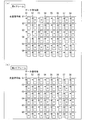
- FIG. 7 is a structural diagram showing the structure of scanning signal lines, data signal lines, and pixel electrodes in a display panel, wherein (a) shows the polarity of the voltage of each pixel electrode in a certain frame (nth frame); b) shows the polarity of the voltage of each pixel electrode when source inversion is performed in the next frame ((n + 1) th frame).
- FIG. 7 is a structural diagram showing the structure of scanning signal lines, data signal lines, and pixel electrodes in a display panel, wherein (a) shows the polarity of the voltage of each pixel electrode in a certain frame (nth frame); b) shows the polarity of the voltage of each pixel electrode when source inversion is performed in the next frame ((n + 1) th frame).
- FIG. 7 is a structural diagram showing the structure of scanning signal lines, data signal lines, and pixel electrodes in a display panel, wherein (a) shows the polarity of the voltage of each pixel electrode in a certain frame (nth frame); b)
- FIG. 7 is a structural diagram showing the structure of scanning signal lines, data signal lines, and pixel electrodes in a display panel, wherein (a) shows the polarity of the voltage of each pixel electrode in a certain frame (nth frame); b) shows the polarity of the voltage of each pixel electrode when line inversion is performed in the next frame ((n + 1) th frame).
- FIG. 7 is a structural diagram showing the structure of scanning signal lines, data signal lines, and pixel electrodes in a display panel, wherein (a) shows the polarity of the voltage of each pixel electrode in a certain frame (nth frame); b) shows the polarity of the voltage of each pixel electrode when dot inversion is performed in the next frame ((n + 1) th frame).
- FIGS. 1 to 10 An embodiment of the present invention will be described with reference to FIGS. 1 to 10 as follows.
- FIG. 8 is a block diagram showing details of the configuration of the electronic apparatus 1 according to the present embodiment.
- the electronic apparatus 1 includes a display device 2, a detection device 3, and a system side control unit 10.
- the display device 2 includes a display panel 2a, a scanning line driving circuit (gate driver, driving means) 4, a signal line driving circuit (source driver, driving means) 5, a common electrode driving circuit 6, and a timing controller 7 (control). Circuit, driving means).
- the detection device 3 includes a detection unit 8 and a detection unit control unit 9 that controls the detection unit 8.
- the detection device 3 may be a touch panel provided on the screen of the display device 2.
- a projection capacitive touch panel is used as the detection device 3.
- the detection unit 8 detection part
- the detection unit 8 detection part
- ITO Indium Tin Oxide
- the detection unit control unit 9 the control unit for performing the detection
- a projection capacitive touch panel is used as the detection device 3, but a touch panel of an arbitrary detection method such as a surface capacitive method or a resistive film method may be used. it can. Note that, in the case of the projected capacitance method, a large number of electrode patterns are formed on the detection unit 8 and thus are easily influenced by driving in the display panel 2a. Therefore, a more remarkable effect can be expected by applying the display device 2 of the present invention to the electronic device 1 including the projected capacitive touch panel.
- the touch panel as the detection device 3 may detect that a user's finger or the like touches or approaches any position on the screen. In this case, it is only necessary to detect the contact or approach, and it is not necessary to detect the position.
- the detection device 3 may be an RF reception device that detects a radio wave flying from the outside and receives a signal included in the radio wave.
- a touch panel is used as the detection device 3, but the present invention can be applied to any detection device.
- the detection device include an RF (Radio Frequency) reception device that receives (detects) radio waves flying from an external device, in addition to the touch panel.
- the RF receiver is also affected by EMI (ElectroMagnetic Interference) radiated from the display device when receiving radio waves. For this reason, when the display device is in the sleep mode, the RF receiving device performs radio wave reception (detection) operation, whereby the accuracy of the received signal can be improved.
- EMI ElectroMagnetic Interference
- the detection unit 8 may include an antenna (not shown).
- the display panel 2a includes a screen composed of a plurality of pixels arranged in a matrix.
- the display panel 2a includes N (N is an arbitrary integer) scanning signal lines G (gate lines) for selecting and scanning the screen in a line-sequential manner.
- the display panel 2a includes M (M is an arbitrary integer) data signal lines S (source lines) that supply data signals to pixels for one row included in the selected line.
- the scanning signal line G and the data signal line S are orthogonal to each other.
- G (n) shown in FIG. 8 represents the n-th (n is an arbitrary integer) scanning signal line G.
- G (0), G (1), and G (2) represent the first, second, and third scanning signal lines G, respectively.
- S (i) represents the i-th data signal line S (i is an arbitrary integer).
- S (0), S (1), and S (2) represent the first, second, and third data signal lines S, respectively.
- the scanning line driving circuit 4 sequentially scans each scanning signal line G from the top to the bottom of the screen, for example. At this time, a rectangular wave for turning on a switching element (TFT) provided in the pixel and connected to the pixel electrode is output to each scanning signal line G. Thereby, the pixels for one row in the screen are selected.
- TFT switching element
- the scanning in the scanning line driving circuit 4 is not limited to the above-described sequential scanning. For example, after scanning odd-numbered scanning signal lines such as the first, third, fifth,..., The second, fourth, sixth,.
- the signal line drive circuit 5 calculates the value of the voltage to be output to each pixel for the selected row from the video signal (arrow A) input from the system-side control unit 10, and sets the voltage of that value to each value. Output to the data signal line S. As a result, image data is supplied to each pixel on the selected scanning signal line G.
- the display device 2 includes a common electrode (not shown) provided for each pixel in the screen.
- the common electrode driving circuit 6 outputs a predetermined common voltage for driving the common electrode to the common electrode based on a signal (arrow B) input from the timing controller 7 (arrow C).
- the timing controller 7 Based on the horizontal and vertical synchronization signals (arrow D, video synchronization signal) input from the system-side control unit 10, the timing controller 7 provides each circuit with a reference signal for each circuit to operate in synchronization. Output. Specifically, a gate start pulse signal and a gate clock signal are output to the scanning line driving circuit 4 based on the vertical synchronization signal (arrow E). Based on the horizontal synchronizing signal, the signal line driving circuit 5 outputs a source start pulse signal, a source latch strobe signal, a source clock signal, and a video signal corresponding to the input image (arrow F).
- the scanning line drive circuit 4 starts scanning the display panel 2a with the gate start pulse signal received from the timing controller 7 as a cue, and according to the gate clock signal which is a signal for selecting the scanning signal line G, each scanning signal line G The selection voltage is sequentially applied to.
- the signal line drive circuit 5 stores the input image data of each pixel in a register according to the source clock signal. Then, after storing the image data, the signal line driving circuit 5 supplies the image data signal to each data signal line S of the display panel 2a according to the next source latch strobe signal.
- an analog amplifier included in the signal line driving circuit 5 is used to supply the image data signal.
- the timing controller 7 outputs a pause drive control signal (arrow G), which is a signal for controlling whether or not the analog amplifier is paused, to the signal line drive circuit 5. At the same time, the timing controller 7 outputs a TP detection operation control signal (arrow H) corresponding to the pause drive control signal to the detection unit control unit 9 of the detection device 3.
- a pause drive control signal (arrow G)
- TP detection operation control signal (arrow H)
- the detection unit control unit 9 when the detection unit control unit 9 receives the TP detection operation control signal, detection by the detection unit 8 is performed. Receiving the TP detection operation control signal, the detection unit control unit 9 drives the detection unit 8 via the drive line Tx.
- the detection unit 8 is a projected capacitive touch panel, for example, and detects a position where a human finger including a user (user of the electronic device 1) or a touch pen (pen) is in contact with or approached. To do.
- the detection unit 8 detects an operation corresponding to the tracing operation (or touching operation) and the human operation by tracing the detection unit 8 (or touching operation) with the human finger or the touch pen. Is done.
- human is not limited to the user of the electronic device 1.
- an observer who observes the display device 2 of the electronic device 1 together with the user of the electronic device 1 is also included in the above-mentioned “human”.
- the detection result by the detection unit 8 is transmitted to the detection unit control unit 9 via the sense line Rx.
- the detection part control part 9 transmits the detection result by the detection part 8 to the system side control part 10 as detection data (arrow I).
- a voltage necessary for the operation of each circuit in the display device 2 is supplied from, for example, a power generation circuit (not shown).
- This power generation circuit is included in the system-side control unit 10. Also good.
- each voltage is supplied from the system side control unit 10 to the display device 2, and each voltage is supplied from the system side control unit 10 to the detection device 3.
- the power supply voltage Vdd is supplied to the signal line driver circuit 5.
- the plurality of pixels cross the plurality of scanning signal lines G extending in one direction and the plurality of data signal lines S extending in the other direction. It is provided corresponding to the part.
- the display device 2 of the electronic apparatus 1 includes a scanning line driving circuit 4 that sequentially applies a gate clock signal (selection signal), which is a signal for selecting the scanning signal line G, to each scanning signal line G.
- a gate clock signal selection signal
- the display device 2 of the electronic apparatus 1 includes a signal line drive circuit 5 that supplies an image data signal to each data signal line S.
- the display device 2 of the electronic device 1 includes a timing controller 7.
- the timing controller 7 outputs the selection signal to the scanning line driving circuit 4 based on the vertical synchronization signal input from the outside (that is, from the system-side control unit 10).
- the timing controller 7 generates a source latch strobe signal (supply instruction signal) which is a signal for instructing the supply of the image data signal based on a horizontal synchronization signal input from the outside (that is, from the system control unit 10). Is output to the signal line drive circuit 5.
- the timing controller 7 detects the detection device 3 that detects the detection target of at least one of the input by touching or approaching the screen and the radio wave flying from the outside of the display device.
- a TP detection operation control signal (detection instruction signal) instructing detection is output a plurality of times in at least one non-scanning period.
- FIG. 1 is a timing chart illustrating a driving method of the display device 2 according to the first embodiment.
- one frame period Tf includes a blanking period in addition to a period for scanning one frame of image data.
- one frame period Tf is substantially equal to one cycle of the vertical synchronization signal.
- a certain amount of deviation may occur between the one frame period Tf and one cycle of the vertical synchronization signal.
- the one frame period Tf before being input to the frame memory may be different from the one frame period Tf after being input to the frame memory.
- the one frame period Tf shown in FIG. 1 is an example, and the one frame period Tf is not necessarily equal to one cycle of the vertical synchronization signal.
- the timing controller 7 has a frame memory.
- the timing controller 7 has a clock generation circuit. Then, scanning is performed after one horizontal period and one vertical period are determined based on the clock signal generated by the clock generation circuit. As a result, display is possible without depending on the synchronization signal input from the outside of the display device 2. However, after the display device 2 has a frame memory, scanning based on the synchronization signal may be performed.
- the level of the vertical synchronization signal changes from, for example, a high level to a low level. This change in signal level corresponds to the falling edge of the pulse.
- the level of the vertical synchronization signal changes from, for example, a high level to a low level at the start time.
- the above-described change in signal level occurs for each one frame period Tf, and the above pulse is included.
- the display panel 2a of the display device 2 in the first embodiment takes the first state and the second state alternately.
- the first state and the second state will be described below.
- a period (scanning period) in which the display panel 2a is in the first state is shown as a scanning frame in FIG.
- a period (non-scanning period) in which the display panel 2a is in the second state is shown as a pause frame in FIG.
- the scanning frame and the pause frame are alternately repeated.
- the driving method of the display device 2 in the first embodiment the following driving is performed. That is, in the pause frame of the display panel 2a, the TP detection operation control signal input from the timing controller 7 to the detection unit control unit 9 of the detection device 3 includes a plurality of pulses for instructing detection (FIG. 1). Shows two examples). Accordingly, for example, the detection unit 8 which is a projected capacitive touch panel performs the detection a plurality of times in the pause frame (that is, the non-scanning period) (FIG. 1 illustrates two detections). ).
- a touch panel detection period Ttp (a period required for detection by the detection unit 8) shown in the waveform of the touch panel detection state is shorter than the touch panel detection period of FIG. This point will be described.
- a technique has been devised that significantly shortens the touch panel detection period (specifically, it is shortened to approximately equal to 1 msec). Therefore, as shown in FIG. 1, a plurality of detections can be realized in one pause frame.
- the start time and end time of the touch panel detection period Ttp may be any period in which the detection instruction signal is active. That is, as shown in FIG. 1, for the touch panel detection period Ttp, it is only necessary that the start time of the touch panel detection period Ttp is synchronized with the rise time of the TP detection operation control signal.
- the touch panel detection period Ttp is started at the time when the TP detection operation control signal rises, and detection may be performed in a predetermined touch panel detection period Ttp.
- the touch panel detection period Ttp may be determined in advance in the detection device 3, for example.
- the refresh frequency is Tf in one frame period, and refresh is performed once in two frame periods (2 ⁇ Tf) of one scanning frame and one pause frame that follows. 1 / (2 ⁇ Tf) (2) It becomes.
- the detection by the detection unit 8 is performed twice in a two-frame period (2 ⁇ Tf) including one scanning frame and one subsequent pause frame. Therefore, the detection frequency indicating the detection frequency of the detection unit 8 is 2 / (2 ⁇ Tf) (3) Thus, it becomes twice the refresh frequency expressed by the equation (2).
- the detection frequency can be 120 Hz. Therefore, it can respond to the handwriting which requires the detection frequency of 100 Hz or more.
- the refresh frequency of the display device 2 according to the first embodiment is refreshed 60 times in a 120 frame period (120 ⁇ Tf). 60 / (120 ⁇ Tf) (4) It becomes.
- the detection by the detection unit 8 is performed 61 times in a 120 frame period (120 ⁇ Tf). That is, since only one frame is detected twice, the number of detections is increased only once.
- the detection frequency indicating the detection frequency of the detection unit 8 is 61 / (120 ⁇ Tf) (5) Thus, it becomes higher than the refresh frequency expressed by the equation (4).
- the detection frequency of the equation (5) is a frequency in the case where detection is performed twice in only one frame out of 60 pause frames. By increasing the number of pause frames in which detection is performed twice to two or more, Furthermore, the detection frequency can be increased.
- the detection instruction signal for instructing the detection is output a plurality of times in at least one of the pause frames. That is, the method for driving the display device 2 according to the first embodiment includes a step of outputting a detection instruction signal for instructing the detection a plurality of times in at least one of the pause frames.
- the detection frequency indicating the detection frequency can be made higher (for example, twice) than the refresh frequency indicating the update frequency of the plurality of pixels.
- the detection frequency can be 120 Hz. Therefore, for example, it is possible to handle handwriting that requires a detection frequency of 100 Hz or more.
- the detection frequency can be not only doubled, but can also be adjusted in the range of 61 Hz to 120 Hz when the refresh frequency is 60 Hz.
- all the above detections are performed in pause frames. That is, all touch panel detection periods Ttp are included in any pause frame. Thereby, it is possible to eliminate the influence of noise caused by scanning in the display device 2 between scanning frames. Therefore, it is possible to greatly improve the accuracy of the detection.
- the display device 2 and the display device 2 driving method capable of realizing the detection operation in the detection device at a frequency higher than the refresh frequency of the display device and the improvement of the detection accuracy.
- the detection device 3 sets the timing of each detection so that the difference between the two detection intervals consecutive in the pause frame and the two detection intervals continuous in the period including the scanning period is minimized. You may decide. Taking the driving shown in the timing chart of FIG. 1 as an example, the detection device 3 may determine the timing of each detection so that the time T1 and the time T2 are minimized.
- this scanning period is indicated as a scanning frame.
- a period during which no scanning is performed that is, a non-scanning period is equal to one frame period Tf
- this non-scanning period is indicated as a pause frame.
- the scanning period and the non-scanning period are not limited to one frame period Tf.
- the idea of the present invention is that the detection frequency is higher than the refresh frequency because the detection unit 8 performs detection a plurality of times in at least one non-scanning period while the scanning period and the non-scanning period are alternately repeated. There is to do.
- the scanning line driving circuit 4, the signal line driving circuit 5, and the timing controller 7 may invert the polarity of the voltage applied to the pixel within the scanning period. .
- dot inversion driving which is driving with a large current consumption during the scanning period, the detection accuracy can be improved and the power consumption of the detection device 3 can be reduced.
- the polarity inversion driving in the display device 2 will be described.
- the pixel electrode in the display panel 2a changes the polarity of the voltage every frame period of a predetermined number of times (for example, once). It is desirable to reverse.
- An inversion method in which a voltage having the same polarity is applied to all the pixel electrodes of the display panel 2a in a certain frame, a voltage having a reverse polarity is applied in the next frame of the certain frame, and this is repeated is “ This is called “frame inversion”.
- Frame inversion can be realized by inverting the polarity of the voltage applied to all data signal lines S in a certain frame every frame period.
- This inversion includes “source inversion”, “line inversion”, “dot inversion”, and the like.
- source inversion includes “source inversion”, “line inversion”, “dot inversion”, and the like.
- FIGS. 11 to 14 are structural diagrams showing the structures of the scanning signal line G, the data signal line S, and the pixel electrode in the display panel 2a.
- (a) shows the polarity of the voltage of each pixel electrode in a certain frame (nth frame), and (b) shows the next frame ((n + 1) th frame).
- the frame polarity indicates the polarity of the voltage of each pixel electrode to which a reverse polarity voltage is applied.
- the polarity of the voltage of each pixel electrode is indicated by + (plus) and-(minus) in the figure.
- FIG. 11 shows an example of source inversion.
- the polarity of the voltage applied to each data signal line (source line) S is inverted.
- the polarity of the voltage can be reversed for each pixel electrode arranged in the direction of the scanning signal line G.
- FIG. 12 shows the same source inversion as in FIG. 11, but the arrangement of the pixel electrodes is different from that in FIG.
- the pixel electrode connected to the data signal line S is disposed on one side (the right side in the illustrated example) with respect to the data signal line S.
- the pixel electrodes connected to the data signal line S are arranged in a staggered manner with respect to the data signal line S. For this reason, the polarities of the voltages of the pixel electrodes arranged between the adjacent data signal lines S are the same in the arrangement of FIG. 11, but are different in the arrangement of FIG.
- FIG. 13 shows an example of line inversion.
- the polarity of the voltage applied to the data signal line S is inverted for each scanning signal line G to be driven (every horizontal scanning period).
- the polarity of the voltage can be reversed for each pixel electrode arranged in the direction of the data signal line S.
- FIG. 14 shows an example of dot inversion.
- the dot inversion can be realized by combining the source inversion shown in FIG. 11 and the line inversion shown in FIG. Specifically, when the first scanning signal line G1 is driven, the polarity of the voltage applied to each data signal line S is changed to the plus (+), and thereafter, the polarity is reversed in order. Next, when the second scanning signal line G2 is driven, the polarity of the voltage applied to each data signal line S is set to minus ( ⁇ ) for the first, and thereafter is inverted in order. Then, by repeating the same in driving the third and subsequent scanning signal lines G, the polarity of the voltage between the pixel electrodes adjacent to each other in the direction of the scanning signal line G and the direction of the data signal line S as shown in FIG. Can be different.
- FIG. 2 is a timing chart illustrating a driving method of the display device 2 according to the second embodiment.
- the non-scanning period is one frame period Tf with one pause frame.
- the non-scanning period includes a plurality of pause frames (a non-scanning period obtained by multiplying one frame period Tf by a plurality of times (corresponding to a plurality of times)). It is.
- the scan frame is followed by two pause frames, that is, a first pause frame (first frame period) and a second pause frame (second frame period). .
- the non-scanning period is a period that is an integral multiple of one frame period Tf (a period corresponding to an integral multiple) (in FIG. 2, the one frame period Tf).
- the period is twice (a period corresponding to twice, 2 ⁇ Tf)).
- the detection is performed a plurality of times as in the first embodiment.
- the detection is performed a plurality of times in the entire non-scanning period constituted by the pause frames of integer multiples.
- the detection device 3 since it is not necessary to perform detection a plurality of times in all pause frames (all periods having a length corresponding to the scanning period), for example, the detection device 3 having the detection unit 8 that is a projected capacitive touch panel. Thus, power consumption can be reduced.
- the timing for starting detection in the first pause frame and the timing for starting detection in the second pause frame are equal. That is, in the first pause frame, the time from when the vertical synchronization signal rises until detection starts is equal to the time from when the vertical synchronization signal rises in the second pause frame until detection starts. To do.
- the touch panel detection period Ttp in the second pause frame may be moved into the first pause frame (may be moved as indicated by a broken line in the touch panel detection state in FIG. 2).
- the above information may be transmitted from the timing controller 7 to the detection unit control unit 9 of the detection device 3 through a route similar to the route (arrow H) through which the TP detection operation control signal is transmitted.
- the detection device 3 may have a function of obtaining the information from the display device 2. Further, the information may be transmitted through a route of the timing controller 7 ⁇ the system side control unit 10 ⁇ the detection unit control unit 9.
- speed information which is information about the speed of movement of the human finger or touch pen touching the detection unit 8
- speed information can be obtained from a change in position coordinates in the detection unit 8.
- the detection device 3 may detect the number of times according to the speed information. For example, when the moving speed of the human finger or the touch pen becomes faster, the number of detections may be increased than before the moving speed becomes faster.
- FIG. 3 is a timing chart illustrating a method for driving the display device 2 according to the third embodiment.
- the detection start timing is constant. That is, the time from when the vertical synchronizing signal rises (from the start time of one frame period Tf) until the detection starts is kept constant.
- the scanning frame is followed by two pause frames, that is, a first pause frame (first half) and a second pause frame (second half). The same as in the second embodiment.
- the time Tp1 from the rise of the vertical synchronization signal to the start of detection is the time from the rise of the vertical synchronization signal to the start of detection in the second pause frame. It is set shorter than Tp2. That is, the detection start time (Tp1) in the first pause frame is earlier than the detection start time (Tp2) in the second pause frame.
- the detection by the detection unit 8 can be performed periodically.
- Regular means that the interval between two consecutive detections is equal for all detections.
- the periodic detection in the driving method of the display device 2 according to the third embodiment will be specifically described.
- the time from the end time of detection to the end time of the first pause frame is Tf-Ttp-Tp1 (6) It becomes.
- T3 which is the time obtained by adding the time tp2 to the time of the expression (6) is expressed by the following expression (7).
- the time from the end time of detection to the end time of the second pause frame is: Tf-Ttp-Tp2 (8) It becomes.
- a time T3 obtained by adding one frame period Tf of the scanning frame and the time tp1 to the time of the formula (8) is represented by the following formula (9).
- the time represented by the equation (9) is a time from the detection end time in the second pause frame to the detection start time in the next first pause frame via the scanning frame.
- the times Tp1 and Tp2 are appropriately set so that Thereby, the said detection in the detection part 8 can be performed regularly.
- FIG. 4 is a timing chart illustrating a driving method of the display device 2 according to the fourth embodiment.
- the non-detection period is an odd number of pause frames (odd number of frames) configured by an odd multiple of one frame period Tf (a period corresponding to an odd multiple). Period).
- the detection start time and the detection end time are the same in each of the odd-numbered pause frames (odd-numbered periods having a length corresponding to the scanning period) in the odd-numbered pause frames. Thereby, the detection in the detection part 8 can be regularly performed similarly to the said Example 3.
- the periodic detection in the driving method of the display device 2 according to the fourth embodiment will be specifically described.
- the time from the end time of detection to the end time of the first pause frame is Tf-Ttp-Tp (11) It becomes.
- a time T4 obtained by adding one frame period Tf of the second pause frame and time tp of the third pause frame to the time of the expression (11) is expressed by the following expression (12).
- the time represented by the expression (12) is a time from the detection end time in the first pause frame to the detection start time in the third pause frame.
- the time from the detection end time to the end time of the third pause frame is Tf ⁇ Ttp ⁇ Tp (13 ) It becomes.
- the time represented by the equation (14) is from the detection end time in the third pause frame to the detection start time in the next first pause frame (or the fifth pause frame if the pause frame is 5 frames or more). It will be time to show.
- the detection in the detection unit 8 is periodically performed in the drive of the display device 2 according to the fourth embodiment. It is clear.
- the above description is for the case where there are three pause frames. However, the description can be similarly applied to the case where the number of pause frames is an odd number of 5 or more, and the intervals between two consecutive detections are all equal. Become. Therefore, the detection in the detection unit 8 can be performed periodically.
- FIG. 5 is a timing chart illustrating a driving method of the display device 2 according to the fifth embodiment.
- the period of one scanning frame and the period of one pause frame are both one frame period Tf.
- time T1 and time T2 are not equal.
- time T1 and time T2 are not equal, and detection is not periodic.
- the time T1 is the time from the end time of a certain touch panel detection period Ttp to the start time of the next touch panel detection period Ttp.
- T2 is the time from the end time of the last touch panel detection period Ttp in a certain pause frame to the start time of the first touch panel detection period Ttp in the next pause frame via the scanning frame.
- the scanning frame (scanning period) is shorter than one frame period Tf.
- This scanning period is the scanning frame (scanning period Td) in FIG.
- the non-scanning period is lengthened from the one frame period Tf by the shortened scanning period.
- This non-scanning frame (non-scanning period) is a non-scanning frame (non-scanning period Ts) in FIG.
- the first detection is started at the end time of the scanning period Td, and after a predetermined time (Tint described later) has elapsed after the end of the first detection, The second detection is started.
- Td + Ts 2 ⁇ Tf (15) Is established.
- Ts is a non-scanning period
- Ttp is a touch panel detection period (a period required for the detection).
- Tint is the time from the end time of detection started at the same time as the end of the scanning period Td to the start time of the next detection (two consecutive detection intervals in the non-scanning period, the predetermined time described above).
- the detection is periodically performed by the non-scanning period Ts that is longer than one frame period Tf and shorter than two frame periods (2 ⁇ Tf).
- Ts that is longer than one frame period Tf and shorter than two frame periods (2 ⁇ Tf).
- periodic detection can be realized only by making one pause frame longer by just making the scanning period shorter (by making the non-scanning period longer than one frame period Tf).
- the interval between two consecutive detections is shortened. More specifically, two consecutive frames are used as compared with a case where periodic detection is realized by a plurality of pause frames (that is, by a non-scanning period of 2 frame periods (2 ⁇ Tf) or more) (Examples 3 and 4). The interval between the two detections becomes shorter. Therefore, smooth detection can be realized.
- the non-scanning frame may be longer than the scanning frame.
- the interval between two consecutive detections can be kept constant, and the above-described detection can be realized periodically. Or, the interval between two consecutive detections can be made almost constant, and the above-described detection can be realized on a regular basis. That is, periodic or substantially periodic detection can be realized simply by making the non-scanning frame longer than the scanning frame. Therefore, smooth detection can be realized.
- FIG. 6 is a timing chart illustrating a driving method of the display device 2 according to the sixth embodiment.
- FIG. 7 is an explanatory diagram illustrating the configuration of the display device 2 according to the sixth embodiment.
- the timing controller 7 outputs a TP detection operation control signal (arrow H) having the same timing as that of the pause drive control signal to the detection unit control unit 9 of the detection device 3.
- the timing controller 7 receives a video signal (clock signal, synchronization signal, video data signal, etc.) and then sends a synchronization control signal (source start pulse signal, A delay corresponding to scanning of several clocks to several lines is generated until a source latch strobe signal, a source clock signal, and the like are output. This is because time is required for timing generation and image processing in the timing controller 7.
- the scanning line driving circuit 4 includes a number of gate driver units 4 ′ corresponding to the number of scanning signal lines G (two are illustrated in FIG. 7). May be provided.
- the signal line driving circuit 5 includes the number of source driver units 5 ′ (signal line driving unit, detection instruction unit, FIG. 7) corresponding to the number of data signal lines S. 3 may be included).
- These source driver units 5 ′ recognize the scanning period (and driving period) and the non-scanning period (and pause period) more strictly than the timing controller 7 because the delay described above does not exist.
- a TP detection operation control signal may be output from one of the source driver units 5 ′ to the detection unit control unit 9 of the detection device 3 via the connection terminal 20. .
- the TP detection operation control signal is output from the timing controller 7 to the detection unit control unit 9. Therefore, the non-scanning period of the display device 2 can be transmitted to the detection device 3 more accurately. Therefore, the detection operation in the detection unit 8 of the detection device 3 can be controlled more accurately.
- the start time and end time of the touch panel detection period may be a period in which the detection instruction signal is active. That's fine. That is, as shown in the first embodiment and FIGS. 1 to 5 and 6A, for the touch panel detection period Ttp, the start time of the touch panel detection period Ttp is the time when the TP detection operation control signal rises. It only needs to be synchronized.
- the touch panel detection period Ttp is started at the time when the TP detection operation control signal rises, and detection may be performed in a predetermined touch panel detection period Ttp.
- the touch panel detection period Ttp may be determined in advance in the detection device 3, for example.
- the touch panel detection period Ttp is determined by the TP detection operation control signal, the detection operation in the detection unit 8 can be controlled more accurately.
- the output of the TP detection operation control signal from the source driver unit 5 ′ to the detection device 3 shown in FIG. 7 and the determination of the touch panel detection period Ttp based on the TP detection operation control signal shown in FIG. And may be combined. As a result, the detection operation in the detection unit 8 can be more accurately controlled.
- FIG. 9 is a block diagram showing details of the configuration of the electronic apparatus 1 ′ according to the present embodiment. The difference between the electronic device 1 and the electronic device 1 ′ is the path of the TP detection operation control signal.
- the TP detection operation control signal is directly output from the timing controller 7 to the detection unit control unit 9 of the detection device 3.
- the TP detection operation control signal is output to the detection unit control unit 9 of the detection device 3 through the system side control unit 10.
- the timing controller 7 outputs a first TP detection operation control signal (arrow H1) to the system-side control unit 10.
- the system-side control unit 10 that has received the first TP detection operation control signal outputs a second TP detection operation control signal (arrow H2) having the same timing as the first TP detection operation control signal to the detection unit control unit 9 of the detection device 3. Output to.
- a delay is generated by the amount via the system-side control unit 10.
- signal processing such as inversion of the signal level is performed on the first TP detection operation control signal, for example, a delay is caused by this signal processing.
- the delay time between the first TP detection operation control signal and the second TP detection operation control signal due to these delays that is, the delay caused by passing through the system control unit 10 or the delay caused by signal processing in the system control unit 10. Tdelay occurs.
- the electronic device 1 ′ in FIG. 9 outputs each TP detection operation control signal in consideration of the delay time Tdelay as shown in FIG. 10, for example. That is, the timing controller 7 outputs the first TP detection operation control signal (arrow H1) to the system-side control unit 10 earlier than the start time of the touch panel detection period Ttp by the delay time Tdelay.
- the system-side control unit 10 that has received the first TP detection operation control signal performs the above-described signal processing on the first TP detection operation control signal as necessary to generate a second TP detection operation control signal. It outputs to the detection part control part 9.
- the time when the delay time Tdelay has elapsed from the time when the first TP detection operation control signal is output can be set as the start time of the touch panel detection period Ttp.
- the plurality of pixels includes the plurality of scanning signal lines G extending in one direction and the plurality of data signal lines S extending in the other direction. It is provided corresponding to the intersection.
- the display device 2 of the electronic apparatus 1 ′ includes a scanning line driving circuit 4 that sequentially applies a gate clock signal (selection signal) that is a signal for selecting the scanning signal line G to each scanning signal line G.
- a gate clock signal selection signal
- the display device 2 of the electronic apparatus 1 ′ includes a signal line driving circuit 5 that supplies an image data signal to each data signal line S.
- the display device 2 of the electronic apparatus 1 ′ includes a timing controller 7 (control circuit).
- the timing controller 7 outputs the selection signal to the scanning line driving circuit 4 based on the vertical synchronization signal input from the outside (that is, from the system-side control unit 10).
- the timing controller 7 outputs a source latch strobe signal (supply instruction signal), which is a signal instructing the supply of the image data signal, to the signal line drive circuit 5 based on a horizontal synchronization signal input from the outside.
- the timing controller 7 sends a TP detection operation control signal (detection instruction signal), which is a signal instructing to perform the detection a plurality of times, to the system-side control unit 10 (overall control unit) in at least one non-scanning period.
- TP detection operation control signal detection instruction signal
- the system-side control unit 10 supplies the vertical synchronization signal and the horizontal synchronization signal.
- the detection device 3 can perform the detection a plurality of times in at least one non-scanning period.
- the display device 2 capable of realizing the detection operation in the detection device at a frequency higher than the refresh frequency of the display device and the improvement in detection accuracy.
- the signal line driving circuit 5 may include the number of source driver units 5 ′ corresponding to the number of data signal lines S. Then, a TP detection operation control signal (second TP detection operation control signal) is transmitted from one of the source driver units 5 ′ to the detection unit control unit 9 of the detection device 3 via the connection terminal and the system-side control unit 10. ) May be output. Thereby, it is possible to more accurately control the detection operation in the detection unit 8 of the detection device 3, excluding the influence of the delay when outputting the TP detection operation control signal from the timing controller 7 to the detection unit control unit 9. It becomes.
- the detection device 3 according to the present embodiment is not necessarily detectable only during a period in which the TP detection operation control signal (detection instruction signal) is valid. That is, the detection device 3 according to the present embodiment is obtained in a period in which the TP detection operation control signal (detection instruction signal) is valid after performing the detection operation itself regardless of the scanning period or the non-scanning period.
- the detection result may be calculated using only data.
- the display panel 2a according to the present embodiment may be a liquid crystal panel including a liquid crystal layer.
- the display device 2 according to the present embodiment is a liquid crystal display device.
- the pixel of the display panel 2a according to the present embodiment may include an organic EL (Electroluminescence) diode that is an element that emits light with luminance according to the flowing current.
- the display device 2 according to the present embodiment is an organic EL display (organic electroluminescence display device).
- the detection device 3 performs the detection a plurality of times in at least one non-scanning period. Accordingly, it is possible to provide a display device that can realize the detection operation in the detection device at a frequency higher than the refresh frequency of the display device and the improvement of detection accuracy.
- the display panel 2a includes a plurality of pixels arranged in a matrix.
- the display panel 2a includes a switching element (TFT) provided in the pixel and connected to the pixel electrode.
- TFT switching element
- the scanning line driving circuit 4 sequentially scans each scanning signal line G from the top to the bottom of the screen, for example. At this time, a rectangular wave for turning on the TFT is output to each scanning signal line G. Thereby, the pixels for one row in the screen are selected.
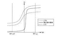
- FIG. 15 is a diagram showing characteristics of various TFTs.
- FIG. 15 shows the characteristics of a TFT using an oxide semiconductor, a TFT using a-Si (amorphous silicon), and a TFT using LTPS (Low Temperature Poly-Silicon).
- the horizontal axis (Vgh) indicates the voltage value of the on-voltage supplied to the gate in each TFT
- the vertical axis (Id) indicates the amount of current between the source and drain in each TFT.
- a period indicated as “TFT-on” in the figure indicates a period in which the transistor is on according to the voltage value of the on-voltage
- a period indicated as “TFT-off” in the figure Indicates a period in which it is in an OFF state according to the voltage value of the ON voltage.
- a TFT using an oxide semiconductor has a higher current amount (that is, electron mobility) in an on state than a TFT using a-Si.
- a TFT using a-Si has an Id current of 1 uA when the TFT is turned on, whereas a TFT using an oxide semiconductor is used when the TFT is turned on.
- the Id current is about 20 to 50 uA. From this, it can be seen that a TFT using an oxide semiconductor has an electron mobility about 20 to 50 times higher in an on state than a TFT using a-Si, and has an excellent on-characteristic. .
- the display device 2 of the present invention by using a TFT using an oxide semiconductor for each pixel, the on characteristics of the TFT of each pixel become very excellent. For this reason, the amount of electron movement when writing pixel data to each pixel can be increased, and the time required for writing can be further shortened. That is, since the display device 2 can shorten the scanning period, a sufficient detection period of the detection device 3 can be ensured accordingly. Therefore, the detection accuracy of the detection device 3 can be further increased.
- the electronic apparatus according to the present invention includes any one of the display devices 2 and the detection device 3, the detection operation in the detection device at a frequency higher than the refresh frequency of the display device and improvement in detection accuracy are realized. I can do it.
- the detection device may minimize a difference between two detection intervals that are continuous in the non-scanning period and two detection intervals that are continuous in a period including the scanning period. You may determine the timing of each detection.
- the non-scanning period may be longer than the scanning period.
- the interval between two consecutive detections can be kept constant, and the above-described detection can be realized periodically. Or, the interval between two consecutive detections can be made almost constant, and the above-described detection can be realized on a regular basis. That is, it is possible to realize regular or substantially regular detection only by making the non-scanning period longer than the scanning period. Therefore, smooth detection can be realized.
- Ts ⁇ Ttp ⁇ 2 + Tint may be established, where Ts is the non-scanning period, Ttp is the period required for the detection, and Tint is the interval between the two detections consecutive in the non-scanning period.
- the periodic detection can be realized by the non-scanning period which is longer than the scanning period and shorter than the period obtained by doubling the scanning period. That is, periodic detection can be realized only by making the non-scanning period longer than the scanning period.
- the interval between two consecutive detections becomes shorter than when periodic detection is realized when the non-scanning period is equal to or longer than a period that is twice the scanning period. Therefore, smooth detection can be realized.
- the plurality of pixels are provided corresponding to intersections of the plurality of scanning signal lines extending in one direction and the plurality of data signal lines extending in the other direction, and the scanning signal lines are selected.
- a scanning line driving circuit that sequentially applies a selection signal that is a signal to be applied to each scanning signal line, a signal line driving circuit that supplies an image data signal to each data signal line, and a vertical synchronization signal input from the outside The selection signal is output to the scanning line driving circuit, and a supply instruction signal, which is a signal for instructing the supply of the image data signal, is supplied to the signal line driving circuit based on a horizontal synchronization signal input from the outside.
- An output control circuit, and the signal line drive circuit has a number of signal line drive units corresponding to the number of the data signal lines, and any one of the signal line drive units includes the detection instruction unit. Be equipped It may be.
- the detection instruction means included in the signal line driving unit outputs the detection instruction signal instructing the detection a plurality of times in at least one non-scanning period. Accordingly, it is possible to provide a display device that can realize the detection operation in the detection device at a frequency higher than the refresh frequency of the display device and the improvement of detection accuracy.
- the detection instruction means included in the signal line drive unit outputs the detection instruction signal from the signal line drive unit to the detection device. Accordingly, it is possible to more accurately control the detection operation in the detection device, excluding the influence of delay when the detection instruction signal is output from the control circuit to the detection device.
- the non-scanning period may be a period equivalent to an integral multiple of the scanning period.
- the detection can be performed a plurality of times in the non-scanning period, which is a period corresponding to an integral multiple of the scanning period. Therefore, the detection frequency indicating the detection frequency can be made higher than the refresh frequency indicating the update frequency of the plurality of pixels.
- the non-scanning period is configured, and it is not necessary to perform the detection a plurality of times in all periods having a length corresponding to the scanning period.
- the non-scanning period is a period obtained by doubling the scanning period,
- the detection start time in the first half of the non-scanning period may be earlier than the detection start time in the second half of the non-scanning period.
- the time from the detection end time in the first half to the detection start time in the second half (in the non-detection period at a certain time, the second detection starts after the first detection ends.
- Time until the detection start time in the next first half to the next detection start time in the first half (in the non-detection period at a certain time, the second detection is completed) Therefore, the time until the first detection is started in the non-detection period following the non-detection period at a certain time can be made equal.
- the non-scanning period is a period obtained by multiplying the scanning period by an odd number, and in each of the odd-numbered periods having a length corresponding to the scanning period among the non-scanning periods, the detection is performed.
- the start time and the end time of the detection may be the same.
- a time from the end time of the detection in the first period to the start time of the detection in the third period, and the end time of the detection in the third period To the time indicating the start time of the detection in the first period after the scanning period.
- the intervals between the two consecutive detections are all equal thereafter.
- the plurality of pixels are provided corresponding to intersections of the plurality of scanning signal lines extending in one direction and the plurality of data signal lines extending in the other direction, and the scanning signal lines are selected.
- a scanning line driving circuit that sequentially applies a selection signal that is a signal to be applied to each scanning signal line, a signal line driving circuit that supplies an image data signal to each data signal line, and a vertical synchronization signal input from the outside The selection signal is output to the scanning line driving circuit, and a supply instruction signal, which is a signal for instructing the supply of the image data signal, is supplied to the signal line driving circuit based on a horizontal synchronization signal input from the outside.
- a control circuit for outputting, and the control circuit may include the detection instruction means.
- the detection instruction means outputs the detection instruction signal instructing a plurality of detections in at least one non-scanning period. Accordingly, it is possible to provide a display device that can realize the detection operation in the detection device at a frequency higher than the refresh frequency of the display device and the improvement of detection accuracy.
- the plurality of pixels are provided corresponding to intersections of the plurality of scanning signal lines extending in one direction and the plurality of data signal lines extending in the other direction, and the scanning signal lines are selected.
- a scanning line driving circuit that sequentially applies a selection signal that is a signal to be applied to each scanning signal line, a signal line driving circuit that supplies an image data signal to each data signal line, and a vertical synchronization signal input from the outside The selection signal is output to the scanning line driving circuit, and a supply instruction signal, which is a signal for instructing the supply of the image data signal, is supplied to the signal line driving circuit based on a horizontal synchronization signal input from the outside.
- the detection apparatus can perform the detection a plurality of times in at least one non-scanning period.
- the detection instruction means outputs the detection instruction signal instructing a plurality of detections in at least one non-scanning period. Accordingly, it is possible to provide a display device that can realize the detection operation in the detection device at a frequency higher than the refresh frequency of the display device and the improvement of detection accuracy.
- the scanning line driving circuit, the signal line driving circuit, and the control circuit may invert the polarity of the voltage applied to the pixel within the scanning period.
- the display device of the present invention may be a liquid crystal display device.
- the display device of the present invention may be an organic electroluminescence display device.
- the detection instruction means outputs the detection instruction signal instructing a plurality of detections in at least one non-scanning period. Accordingly, it is possible to provide a display device that can realize the detection operation in the detection device at a frequency higher than the refresh frequency of the display device and the improvement of detection accuracy.
- the detection device may be a touch panel provided on the screen of the display device.
- the touch panel By using the touch panel as the detection device, it is possible to detect a position where a user's finger or the like has touched or approached.
- the touch panel is a projected capacitive touch panel.
- the portion to be detected is a transparent electrode pattern in the form of a matrix made of ITO (Indium Tin Oxide) or the like on a transparent substrate such as glass or plastic.
- ITO Indium Tin Oxide
- the control part of the detection part can detect the position where the user's finger or the like has touched or approached by detecting a change in the current or voltage of the transparent electrode pattern.
- the detection device generates speed information of the movement of the detection target on the screen, In at least one non-scanning period, the detection instruction signal may be output a number of times corresponding to the speed information.
- the number of detections by the detection device can be increased. Therefore, even when the moving speed of the detection target is increased, the position can be accurately detected.
- the detection device may be an RF reception device that detects a radio wave flying from the outside and receives a signal included in the radio wave.
- the detection device for example, a touch panel is used, but the present invention can be applied to any detection device.
- this detection device include an RF (Radio Frequency) reception circuit that receives (detects) radio waves flying from an external device, in addition to the touch panel.
- the RF receiving circuit is also affected by EMI (ElectroMagnetic Interference) radiated from the display device when receiving radio waves. For this reason, when the display device is in the sleep mode, the RF receiving circuit performs an operation of receiving (detecting) radio waves, whereby the accuracy of the received signal can be improved.
- EMI ElectroMagnetic Interference
- the pixel included in the display device includes a TFT, and an oxide semiconductor may be used for a semiconductor layer of the TFT.
- the oxide semiconductor may be IGZO.
- the amount of electron movement when writing pixel data to each pixel can be increased, and the time required for writing can be shortened. Accordingly, the display device can shorten the scanning period, and accordingly, the detection device can sufficiently secure the detection period. Therefore, the detection accuracy of the detection device can be further increased.
- the detection apparatus can perform detection operation at a frequency higher than the refresh frequency of the display device and improve detection accuracy. I can do it.
- the display device of the present invention can be applied to a display device that can directly or indirectly control a detection device having a touch panel or an RF receiver.
- a detection device having a touch panel or an RF receiver can be suitably used for a display device that requires a high detection frequency, such as a display device that performs handwriting on a touch panel.
Landscapes
- Engineering & Computer Science (AREA)
- Theoretical Computer Science (AREA)
- General Engineering & Computer Science (AREA)
- Physics & Mathematics (AREA)
- General Physics & Mathematics (AREA)
- Human Computer Interaction (AREA)
- Chemical & Material Sciences (AREA)
- Crystallography & Structural Chemistry (AREA)
- Computer Hardware Design (AREA)
- Control Of Indicators Other Than Cathode Ray Tubes (AREA)
- Position Input By Displaying (AREA)
- Liquid Crystal (AREA)
Abstract
Description
1/(2×Tf) (1)
となる。1つの走査フレームと1つの休止フレームとを合わせた2フレーム期間(2×Tf)において、表示装置のリフレッシュと、検出装置であるタッチパネルにおける検出とは、それぞれ1度ずつ行われるためである。
まず、本実施形態に係る電子機器1の構成について、図8を参照して説明する。図8は、本実施形態に係る電子機器1の構成の詳細を示すブロック図である。図8に示すように、電子機器1は、表示装置2、検出装置3、及び、システム側コントロール部10を備えている。また、表示装置2は、表示パネル2a、走査線駆動回路(ゲートドライバ、駆動手段)4、信号線駆動回路(ソースドライバ、駆動手段)5、共通電極駆動回路6、及び、タイミングコントローラ7(制御回路、駆動手段)を有している。さらに、検出装置3は、検出部8と、検出部8を制御する検出部コントロール部9とを有している。
図1は、本実施例1に係る表示装置2の駆動方法を示すタイミングチャートである。
1/(2×Tf) (2)
となる。
2/(2×Tf) (3)
となり、(2)式で示されるリフレッシュ周波数の2倍となる。
60/(120×Tf) (4)
となる。
61/(120×Tf) (5)
となり、(4)式で示されるリフレッシュ周波数よりも高くなる。
図2は、本実施例2に係る表示装置2の駆動方法を示すタイミングチャートである。
図3は、本実施例3に係る表示装置2の駆動方法を示すタイミングチャートである。
Tf-Ttp-Tp1 (6)
となる。
T3=(Tf-Ttp-Tp1)+Tp2=Tf-Ttp-Tp1+Tp2 (7)
は、第1休止フレームにおける検出の終了時刻から、第2休止フレームにおける検出の開始時刻までを示す時間となる。
Tf-Ttp-Tp2 (8)
となる。
T3=(Tf-Ttp-Tp2)+Tf+Tp1=2×Tf-Ttp+Tp1-Tp2 (9)
(9)式で示される時間は、第2休止フレームにおける検出の終了時刻から、走査フレームを介した次の第1休止フレームにおける検出の開始時刻までを示す時間となる。
Tf-Ttp-Tp1+Tp2=2×Tf-Ttp+Tp1-Tp2 (10)
となるように、時間Tp1,Tp2を適切に設定する。これにより、検出部8における上記検出を定期的に行うことが出来る。
図4は、本実施例4に係る表示装置2の駆動方法を示すタイミングチャートである。
Tf-Ttp-Tp (11)
となる。
T4=(Tf-Ttp-Tp)+Tf+Tp=2×Tf-Ttp (12)
(12)式で示される時間は、第1休止フレームにおける検出の終了時刻から、第3休止フレームにおける検出の開始時刻までを示す時間となる。
Tf-Ttp-Tp (13)
となる。
T4=(Tf-Ttp-Tp)+Tf+Tp=2×Tf-Ttp (14)
(14)式で示される時間は、第3休止フレームにおける検出の終了時刻から、次の第1休止フレーム(または、休止フレームが5フレーム以上であれば第5休止フレーム)における検出の開始時刻までを示す時間となる。
図5は、本実施例5に係る表示装置2の駆動方法を示すタイミングチャートである。
Td+Ts=2×Tf (15)
が成立する。
Ts≧Ttp×2+Tint (16)
を満足する必要がある。(16)式において、Tsは非走査期間であり、Ttpはタッチパネル検出期間(上記検出に要する期間)である。Tintは、走査期間Tdの終了と同時に開始される検出の終了時刻から、次の検出の開始時刻までの時間(非走査期間において連続する2つの上記検出の間隔、上述した所定時間)である。
図6は、本実施例6に係る表示装置2の駆動方法を示すタイミングチャートである。図7は、本実施例6に係る表示装置2の構成を示す説明図である。
図9は、本実施形態に係る電子機器1’の構成の詳細を示すブロック図である。電子機器1と電子機器1’との相違点は、TP検出動作制御信号の経路である。
本実施形態に係る検出装置3は、上記TP検出動作制御信号(検出指示信号)が有効である期間のみ検出可能であるわけではない。即ち、本実施形態に係る検出装置3は、走査期間・非走査期間に関わらず検出動作自体を実施した上で、上記TP検出動作制御信号(検出指示信号)が有効である期間に得られたデータのみを使用して、検出結果として算出しても良い。
本実施形態に係る表示パネル2aは、液晶層を備える液晶パネルであってもよい。この場合、本実施形態に係る表示装置2は、液晶表示装置となる。
表示パネル2aは、マトリクス状に配置された複数の画素を備えている。また、表示パネル2aは、画素に備えられ画素電極に接続されるスイッチング素子(TFT)を備えている。
本発明の電子機器は、上記いずれかの表示装置2と、検出装置3とを備えるので、表示装置のリフレッシュ周波数よりも高い周波数での検出装置における検出動作と、検出精度の向上とを実現することが出来る。
上記表示装置では、上記検出装置は、上記非走査期間において連続する2つの上記検出の間隔と、上記走査期間を含む期間において連続する2つの上記検出の間隔との差が最小となるように、各検出のタイミングを決定してもよい。
上記非走査期間の前半部における上記検出の開始時刻は、上記非走査期間の後半部における上記検出の開始時刻よりも早くてもよい。
少なくとも1つの上記非走査期間において、上記速度情報に応じた回数の上記検出指示信号を出力してもよい。
2 表示装置
2a 表示パネル
3 検出装置
4 走査線駆動回路
4’ ゲートドライバ部
5 信号線駆動回路
5’ ソースドライバ部(信号線駆動部、検出指示手段)
6 共通電極駆動回路
7 タイミングコントローラ(制御回路、検出指示手段)
8 検出部
9 検出部コントロール部
10 システム側コントロール部(統括制御部)
G 走査信号線
Rx センスライン
S データ信号線
Tf 1フレーム期間
Ttp タッチパネル検出期間
Tx 駆動ライン
Claims (20)
- 複数の画素からなる画面を有する表示装置であって、
上記複数の画素が順次選択状態にされる走査が行われる走査期間と、上記走査が全く行われない非走査期間とが交互に繰り返される表示装置において、
上記画面への接触または接近による入力および上記表示装置の外部から飛来する電波の少なくとも何れか一方の検出対象を検出する検出装置に対して、少なくとも1つの上記非走査期間において、上記検出を指示する検出指示信号を複数回出力する検出指示手段を備えることを特徴とする表示装置。 - 上記検出装置は、上記非走査期間において連続する2つの上記検出の間隔と、上記走査期間を含む期間において連続する2つの上記検出の間隔との差が最小となるように、各検出のタイミングを決定することを特徴とする請求項1に記載の表示装置。
- 上記非走査期間は、上記走査期間よりも長いことを特徴とする請求項2に記載の表示装置。
- 上記非走査期間をTs、
上記検出に要する期間をTtp、
上記非走査期間において連続する2つの上記検出の間隔をTintとすると、
Ts≧Ttp×2+Tint
が成立することを特徴とする請求項3に記載の表示装置。 - 上記複数の画素は、一方向に伸びる複数の走査信号線と、他方向に伸びる複数のデータ信号線との交差部に対応して設けられ、
上記走査信号線を選択状態とする信号である選択信号を、各走査信号線に順次印加する走査線駆動回路と、
各データ信号線に画像データ信号を供給する信号線駆動回路と、
外部から入力された垂直同期信号に基づいて、上記選択信号を上記走査線駆動回路に出力するとともに、外部から入力された水平同期信号に基づいて、上記画像データ信号の供給を指示する信号である供給指示信号を、上記信号線駆動回路に出力する制御回路とをさらに備え、
上記信号線駆動回路は、上記データ信号線の本数に応じた数の信号線駆動部を有し、
いずれか1つの上記信号線駆動部は、上記検出指示手段を備えることを特徴とする請求項1~4のいずれか1項に記載の表示装置。 - 上記非走査期間は、上記走査期間の整数倍相当の期間であることを特徴とする請求項1に記載の表示装置。
- 上記非走査期間は、上記走査期間の2倍相当の期間であり、
上記非走査期間の前半部における上記検出の開始時刻は、上記非走査期間の後半部における上記検出の開始時刻よりも早いことを特徴とする請求項6に記載の表示装置。 - 上記非走査期間は、上記走査期間の奇数倍相当の期間であり、
上記非走査期間の内、上記走査期間に相当する長さを有する奇数番目の期間のそれぞれにおいて、上記検出の開始時刻、及び、上記検出の終了時刻が同一であることを特徴とする請求項1に記載の表示装置。 - 上記複数の画素は、一方向に伸びる複数の走査信号線と、他方向に伸びる複数のデータ信号線との交差部に対応して設けられ、
上記走査信号線を選択状態とする信号である選択信号を、各走査信号線に順次印加する走査線駆動回路と、
各データ信号線に画像データ信号を供給する信号線駆動回路と、
外部から入力された垂直同期信号に基づいて、上記選択信号を上記走査線駆動回路に出力するとともに、外部から入力された水平同期信号に基づいて、上記画像データ信号の供給を指示する信号である供給指示信号を、上記信号線駆動回路に出力する制御回路とをさらに備え、
上記制御回路は、上記検出指示手段を備えることを特徴とする請求項1~4,6~8のいずれか1項に記載の表示装置。 - 上記複数の画素は、一方向に伸びる複数の走査信号線と、他方向に伸びる複数のデータ信号線との交差部に対応して設けられ、
上記走査信号線を選択状態とする信号である選択信号を、各走査信号線に順次印加する走査線駆動回路と、
各データ信号線に画像データ信号を供給する信号線駆動回路と、
外部から入力された垂直同期信号に基づいて、上記選択信号を上記走査線駆動回路に出力するとともに、外部から入力された水平同期信号に基づいて、上記画像データ信号の供給を指示する信号である供給指示信号を、上記信号線駆動回路に出力する制御回路と、
上記垂直同期信号及び上記水平同期信号を供給する統括制御部とをさらに備え、
上記制御回路は、上記検出指示信号を、上記統括制御部を介して上記検出装置へ出力することを特徴とする請求項1~4,6~8のいずれか1項に記載の表示装置。 - 上記走査線駆動回路、上記信号線駆動回路、及び、上記制御回路は、上記走査期間内において、上記画素へ印加する電圧の極性を反転させることを特徴とする請求項5,9,10のいずれか1項に記載の表示装置。
- 液晶表示装置であることを特徴とする請求項1~11のいずれか1項に記載の表示装置。
- 有機エレクトロルミネッセンス表示装置であることを特徴とする請求項1~11のいずれか1項に記載の表示装置。
- 上記検出装置は、上記表示装置の画面に設けられるタッチパネルであることを特徴とする請求項1~13のいずれか1項に記載の表示装置。
- 上記検出装置は、上記画面における上記検出対象の移動の速度情報を生成し、
少なくとも1つの上記非走査期間において、上記速度情報に応じた回数の上記検出指示信号を出力することを特徴とする請求項14に記載の表示装置。 - 上記検出装置は、外部から飛来する電波を検出して、該電波に含まれる信号を受信するRF受信装置であることを特徴とする請求項1~13のいずれか1項に記載の表示装置。
- 上記表示装置が有する上記画素は、TFTを備えており、
上記TFTの半導体層には、酸化物半導体が用いられていることを特徴とする請求項1~16のいずれか1項に記載の表示装置。 - 上記酸化物半導体は、IGZOであることを特徴とする請求項17に記載の表示装置。
- 請求項1~18のいずれか1項に記載の表示装置と、
上記検出装置とを備えることを特徴とする電子機器。 - 複数の画素からなる画面を有する表示装置の駆動方法であって、
上記複数の画素が順次選択状態にされる走査が行われる走査期間と、上記走査が全く行われない非走査期間とが交互に繰り返される表示装置の駆動方法において、
上記画面への接触または接近による入力および上記表示装置の外部から飛来する電波の少なくとも何れか一方の検出対象を検出する検出装置に対して、少なくとも1つの上記非走査期間において、上記検出を指示する検出指示信号を複数回出力する工程を含むことを特徴とする表示装置の駆動方法。
Priority Applications (6)
| Application Number | Priority Date | Filing Date | Title |
|---|---|---|---|
| KR1020137014185A KR101326415B1 (ko) | 2011-04-15 | 2012-04-06 | 표시 장치, 표시 장치의 구동 방법 및 전자 기기 |
| US13/984,338 US8872783B2 (en) | 2011-04-15 | 2012-04-06 | Display device, method for driving display device, and electronic equipment |
| JP2013509885A JP5280596B2 (ja) | 2011-04-15 | 2012-04-06 | 表示装置、表示装置の駆動方法及び電子機器 |
| EP12771937.5A EP2698688A4 (en) | 2011-04-15 | 2012-04-06 | DISPLAY DEVICE, METHOD FOR CONTROLLING THE DISPLAY DEVICE AND ELECTRONIC EQUIPMENT THEREWITH |
| CN201280004801.4A CN103299255B (zh) | 2011-04-15 | 2012-04-06 | 显示装置、显示装置的驱动方法以及电子设备 |
| US14/492,287 US9268437B2 (en) | 2011-04-15 | 2014-09-22 | Display device, method for driving display device, and electronic equipment |
Applications Claiming Priority (2)
| Application Number | Priority Date | Filing Date | Title |
|---|---|---|---|
| JP2011091541 | 2011-04-15 | ||
| JP2011-091541 | 2011-04-15 |
Related Child Applications (2)
| Application Number | Title | Priority Date | Filing Date |
|---|---|---|---|
| US13/984,338 A-371-Of-International US8872783B2 (en) | 2011-04-15 | 2012-04-06 | Display device, method for driving display device, and electronic equipment |
| US14/492,287 Continuation US9268437B2 (en) | 2011-04-15 | 2014-09-22 | Display device, method for driving display device, and electronic equipment |
Publications (1)
| Publication Number | Publication Date |
|---|---|
| WO2012141112A1 true WO2012141112A1 (ja) | 2012-10-18 |
Family
ID=47009285
Family Applications (1)
| Application Number | Title | Priority Date | Filing Date |
|---|---|---|---|
| PCT/JP2012/059602 Ceased WO2012141112A1 (ja) | 2011-04-15 | 2012-04-06 | 表示装置、表示装置の駆動方法及び電子機器 |
Country Status (7)
| Country | Link |
|---|---|
| US (2) | US8872783B2 (ja) |
| EP (1) | EP2698688A4 (ja) |
| JP (1) | JP5280596B2 (ja) |
| KR (1) | KR101326415B1 (ja) |
| CN (2) | CN104978064B (ja) |
| TW (1) | TWI421818B (ja) |
| WO (1) | WO2012141112A1 (ja) |
Cited By (7)
| Publication number | Priority date | Publication date | Assignee | Title |
|---|---|---|---|---|
| WO2014084089A1 (ja) * | 2012-11-30 | 2014-06-05 | シャープ株式会社 | タッチパネルコントローラ、並びにこれを用いた電子機器 |
| JP2014132445A (ja) * | 2012-12-05 | 2014-07-17 | Japan Display Inc | タッチ検出機能付き表示装置、その駆動方法及び電子機器 |
| JP2014203346A (ja) * | 2013-04-08 | 2014-10-27 | シャープ株式会社 | 座標位置検出装置及び表示入力装置 |
| JP2015041182A (ja) * | 2013-08-21 | 2015-03-02 | パナソニック株式会社 | 情報入力表示装置 |
| JP2016515255A (ja) * | 2013-03-13 | 2016-05-26 | シナプティクス インコーポレイテッド | 非表示更新期間後の表示アーチファクトの低減 |
| JP2018072821A (ja) * | 2016-10-26 | 2018-05-10 | 株式会社半導体エネルギー研究所 | 表示装置およびその動作方法 |
| CN112447149A (zh) * | 2019-08-30 | 2021-03-05 | 拉碧斯半导体株式会社 | 显示驱动器、显示装置和半导体装置 |
Families Citing this family (52)
| Publication number | Priority date | Publication date | Assignee | Title |
|---|---|---|---|---|
| US9293103B2 (en) * | 2011-04-07 | 2016-03-22 | Sharp Kabushiki Kaisha | Display device, and method for driving same |
| US9449571B2 (en) * | 2012-06-29 | 2016-09-20 | Sharp Kabushiki Kaisha | Display device driving method, display device, and liquid crystal display device |
| KR101951478B1 (ko) * | 2012-07-09 | 2019-02-22 | 엘지전자 주식회사 | 터치 디스플레이 장치 및 멀티 터치 디스플레이 장치 |
| EP2917810A4 (en) * | 2012-11-06 | 2016-06-22 | Hewlett Packard Development Co | INTERACTIVE DISPLAY |
| KR101560535B1 (ko) * | 2012-12-11 | 2015-10-15 | 엘지디스플레이 주식회사 | 터치스크린 일체형 표시장치 및 그 구동 방법 |
| US20140176451A1 (en) * | 2012-12-21 | 2014-06-26 | Barnesandnoble.Com Llc | Method for adaptive scan rate for an electronic device |
| JP6103757B2 (ja) * | 2013-01-28 | 2017-03-29 | シナプティクス・ジャパン合同会社 | タッチ表示制御装置及び情報端末装置 |
| TWI475462B (zh) * | 2013-03-06 | 2015-03-01 | Pixart Imaging Inc | 電容式觸控裝置 |
| US9235285B2 (en) * | 2013-05-13 | 2016-01-12 | Himax Technologies Limited | Pixel matrix, touch display device and drving method thereof |
| TWI507957B (zh) * | 2013-07-22 | 2015-11-11 | Chunghwa Picture Tubes Ltd | 驅動觸控顯示器的方法及提升訊雜比的觸控顯示器 |
| KR102156763B1 (ko) * | 2013-09-27 | 2020-09-16 | 엘지디스플레이 주식회사 | 터치표시장치 및 이의 구동방법 |
| WO2015067166A1 (zh) * | 2013-11-08 | 2015-05-14 | 华为终端有限公司 | 一种触摸式输入方法及装置 |
| US10599831B2 (en) * | 2014-02-07 | 2020-03-24 | Snowshoefood Inc. | Increased security method for hardware-tool-based authentication |
| KR102136692B1 (ko) * | 2014-05-07 | 2020-07-22 | 삼성전자주식회사 | 디스플레이 장치 |
| US9354744B2 (en) * | 2014-06-09 | 2016-05-31 | Sony Corporation | Adaptive touch panel synchronization |
| US9842551B2 (en) * | 2014-06-10 | 2017-12-12 | Apple Inc. | Display driver circuitry with balanced stress |
| CN104063105B (zh) * | 2014-06-11 | 2017-02-15 | 合肥鑫晟光电科技有限公司 | 一种触摸装置及触摸驱动方法 |
| US20160034060A1 (en) * | 2014-07-31 | 2016-02-04 | Himax Technologies Limited | TOUCH DISPLAY DEVICE with multiple alternating touch periods and display periods per frame |
| US9653029B2 (en) | 2014-08-05 | 2017-05-16 | Apple Inc. | Concurrently refreshing multiple areas of a display device using multiple different refresh rates |
| US9779664B2 (en) | 2014-08-05 | 2017-10-03 | Apple Inc. | Concurrently refreshing multiple areas of a display device using multiple different refresh rates |
| KR102226422B1 (ko) * | 2014-10-13 | 2021-03-12 | 삼성디스플레이 주식회사 | 유기 발광 표시 장치 및 이의 구동 방법 |
| WO2016111939A1 (en) * | 2015-01-05 | 2016-07-14 | Synaptics Incorporated | Time sharing of display and sensing data |
| CN104731434B (zh) * | 2015-03-27 | 2018-12-07 | 惠州Tcl移动通信有限公司 | 一种触摸屏防干扰方法、系统和移动终端 |
| KR102161084B1 (ko) * | 2015-07-31 | 2020-10-05 | 엘지디스플레이 주식회사 | 터치 IC(integrated circuit) 및 터치 디스플레이 장치와 이의 구동 방법 |
| CN104991689B (zh) * | 2015-08-10 | 2018-04-24 | 京东方科技集团股份有限公司 | 触控显示面板的驱动方法、装置和触控显示装置 |
| EP3347801A4 (en) * | 2015-09-11 | 2019-03-13 | BOE Technology Group Co., Ltd. | ARRAYSUBSTRAT FOR CAPACITIVE TOUCH SCREEN IN THE CELL AND CONTROL PROCEDURES FOR IT, ASSOCIATED DISPLAY TABLES AND RELATED DISPLAY DEVICE |
| JP6479625B2 (ja) * | 2015-10-13 | 2019-03-06 | 株式会社ジャパンディスプレイ | タッチ検出機能付き表示装置 |
| US9891774B2 (en) * | 2015-12-31 | 2018-02-13 | Synaptics Incorporated | Touch noise canceling for dot-inversion driving scheme |
| US10818698B2 (en) * | 2016-06-09 | 2020-10-27 | Sharp Kabushiki Kaisha | Active matrix substrate and display device and touch panel display device including same |
| US10133403B2 (en) * | 2016-06-29 | 2018-11-20 | Apple Inc. | System and method for variable frame duration control in an electronic display |
| KR102539856B1 (ko) * | 2016-07-28 | 2023-06-08 | 엘지디스플레이 주식회사 | 표시장치와 그 게이트 구동 회로 |
| US10261632B2 (en) | 2016-09-22 | 2019-04-16 | Apple Inc. | Systems and methods for inserting intra-frame pause |
| KR102609072B1 (ko) | 2016-09-23 | 2023-12-04 | 엘지디스플레이 주식회사 | 유기발광표시패널, 유기발광표시장치, 데이터 드라이버 및 저전력 구동 방법 |
| KR102568925B1 (ko) | 2016-10-25 | 2023-08-22 | 엘지디스플레이 주식회사 | 터치센서를 구비하는 표시장치 및 그에 대한 터치감지방법 |
| US11119604B2 (en) * | 2016-11-11 | 2021-09-14 | Sharp Kabushiki Kaisha | Display device and touch sensor with accurate touch detection and low power consumption |
| CN107273130B (zh) * | 2017-06-20 | 2020-08-04 | 深圳市万普拉斯科技有限公司 | 加速界面绘制的方法、装置和终端 |
| KR102467371B1 (ko) * | 2017-11-09 | 2022-11-14 | 엘지디스플레이 주식회사 | 전계발광 표시장치 및 그 제조방법 |
| CN109830213B (zh) * | 2017-11-23 | 2021-12-21 | 奇景光电股份有限公司 | 显示设备 |
| KR102416710B1 (ko) * | 2017-12-08 | 2022-07-05 | 엘지디스플레이 주식회사 | 터치표시장치 및 그 구동방법 |
| JP2019109441A (ja) * | 2017-12-20 | 2019-07-04 | 京セラドキュメントソリューションズ株式会社 | 画像形成装置 |
| JP7041036B2 (ja) * | 2018-09-27 | 2022-03-23 | シャープ株式会社 | タッチパネルディスプレイ及びタッチパネルディスプレイの制御方法 |
| US10775921B2 (en) * | 2019-01-02 | 2020-09-15 | Novatek Microelectronics Corp. | Method of controlling timing for touch and display driver system and touch and display driver system using the same |
| US10895933B2 (en) * | 2019-03-14 | 2021-01-19 | Novatek Microelectronics Corp. | Timing control circuit and operation method thereof |
| CN110176200B (zh) * | 2019-06-11 | 2023-03-21 | 苏州华兴源创科技股份有限公司 | 一种面板检测信号的产生方法和系统 |
| US11176386B2 (en) * | 2019-07-08 | 2021-11-16 | Nxp Usa, Inc. | System and method for continuous operation of vision/radar systems in presence of bit errors |
| CN110473495B (zh) * | 2019-09-12 | 2020-09-18 | 欧姆龙(上海)有限公司 | 发光元件的刷新方法和装置 |
| CN110969976B (zh) * | 2019-11-29 | 2023-03-10 | 厦门天马微电子有限公司 | 显示装置的驱动方法和显示装置 |
| CN111883073B (zh) * | 2020-07-22 | 2022-02-25 | 上海创功通讯技术有限公司 | 一种电子设备的显示方法及电子设备 |
| JP7470797B2 (ja) * | 2020-08-03 | 2024-04-18 | シャープ株式会社 | 表示装置およびその駆動方法 |
| CN112201193B (zh) * | 2020-10-21 | 2023-07-21 | 武汉天马微电子有限公司 | 显示面板的驱动方法、驱动电路和显示装置 |
| CN112908237B (zh) * | 2021-01-29 | 2024-12-13 | 厦门天马微电子有限公司 | 一种显示装置及其驱动方法 |
| CN115657878B (zh) * | 2022-12-08 | 2023-04-25 | 惠科股份有限公司 | 触摸阵列基板、触摸定位方法和显示面板 |
Citations (3)
| Publication number | Priority date | Publication date | Assignee | Title |
|---|---|---|---|---|
| JPH07191806A (ja) * | 1993-12-27 | 1995-07-28 | Sharp Corp | ペン入力機能付き液晶表示装置 |
| JP2000181624A (ja) * | 1998-12-15 | 2000-06-30 | Sharp Corp | 表示一体型タブレット装置 |
| JP2001312253A (ja) | 2000-04-28 | 2001-11-09 | Sharp Corp | 表示装置の駆動方法およびそれを用いた表示装置ならびに携帯機器 |
Family Cites Families (18)
| Publication number | Priority date | Publication date | Assignee | Title |
|---|---|---|---|---|
| JP3834778B2 (ja) * | 1996-05-30 | 2006-10-18 | 日本システム開発株式会社 | 座標入力表示装置 |
| CN1220098C (zh) | 2000-04-28 | 2005-09-21 | 夏普株式会社 | 显示器件、显示器件驱动方法和装有显示器件的电子设备 |
| JP3730159B2 (ja) | 2001-01-12 | 2005-12-21 | シャープ株式会社 | 表示装置の駆動方法および表示装置 |
| JP3918642B2 (ja) * | 2002-06-07 | 2007-05-23 | カシオ計算機株式会社 | 表示装置及びその駆動方法 |
| US7154481B2 (en) * | 2002-06-25 | 2006-12-26 | 3M Innovative Properties Company | Touch sensor |
| AU2003250425A1 (en) * | 2002-09-06 | 2004-03-29 | Koninklijke Philips Electronics N.V. | Touch sensing |
| KR20040085303A (ko) * | 2003-03-31 | 2004-10-08 | 비오이 하이디스 테크놀로지 주식회사 | 액정표시장치의 무선주파수신호 검출장치 및 이를 이용한무선주파수 신호 검출방법 |
| US7589706B2 (en) * | 2004-09-03 | 2009-09-15 | Chen-Jean Chou | Active matrix light emitting device display and drive method thereof |
| KR20060108932A (ko) * | 2005-04-13 | 2006-10-18 | 삼성전자주식회사 | 감지부를 내장하는 표시 장치 및 그 구동 방법 |
| JP4818854B2 (ja) | 2006-09-06 | 2011-11-16 | 京セラ株式会社 | 画像表示装置、電子機器、表示制御装置、及び表示制御方法 |
| JP2008287119A (ja) * | 2007-05-18 | 2008-11-27 | Semiconductor Energy Lab Co Ltd | 液晶表示装置の駆動方法 |
| US8411117B2 (en) * | 2007-12-20 | 2013-04-02 | Sharp Kabushiki Kaisha | Display device having optical sensors |
| KR101533741B1 (ko) * | 2008-09-17 | 2015-07-03 | 삼성디스플레이 주식회사 | 표시패널의 구동방법 및 이를 이용한 표시장치 |
| JP5439059B2 (ja) * | 2009-06-30 | 2014-03-12 | 株式会社ジャパンディスプレイ | 表示装置およびその駆動方法 |
| JP4811502B2 (ja) * | 2009-07-01 | 2011-11-09 | カシオ計算機株式会社 | 液晶表示パネル及びタッチパネル |
| JP5629439B2 (ja) * | 2009-08-26 | 2014-11-19 | 株式会社ジャパンディスプレイ | 液晶表示装置 |
| JP5427648B2 (ja) | 2010-03-02 | 2014-02-26 | 株式会社ジャパンディスプレイ | 座標入力装置、およびそれを備えた表示装置 |
| JP5734805B2 (ja) * | 2011-10-12 | 2015-06-17 | 株式会社ジャパンディスプレイ | 表示装置、駆動回路、駆動方法、および電子機器 |
-
2012
- 2012-04-06 CN CN201510238999.8A patent/CN104978064B/zh active Active
- 2012-04-06 CN CN201280004801.4A patent/CN103299255B/zh active Active
- 2012-04-06 US US13/984,338 patent/US8872783B2/en active Active
- 2012-04-06 WO PCT/JP2012/059602 patent/WO2012141112A1/ja not_active Ceased
- 2012-04-06 KR KR1020137014185A patent/KR101326415B1/ko not_active Expired - Fee Related
- 2012-04-06 EP EP12771937.5A patent/EP2698688A4/en not_active Ceased
- 2012-04-06 JP JP2013509885A patent/JP5280596B2/ja active Active
- 2012-04-13 TW TW101113397A patent/TWI421818B/zh not_active IP Right Cessation
-
2014
- 2014-09-22 US US14/492,287 patent/US9268437B2/en active Active
Patent Citations (3)
| Publication number | Priority date | Publication date | Assignee | Title |
|---|---|---|---|---|
| JPH07191806A (ja) * | 1993-12-27 | 1995-07-28 | Sharp Corp | ペン入力機能付き液晶表示装置 |
| JP2000181624A (ja) * | 1998-12-15 | 2000-06-30 | Sharp Corp | 表示一体型タブレット装置 |
| JP2001312253A (ja) | 2000-04-28 | 2001-11-09 | Sharp Corp | 表示装置の駆動方法およびそれを用いた表示装置ならびに携帯機器 |
Non-Patent Citations (1)
| Title |
|---|
| See also references of EP2698688A4 * |
Cited By (9)
| Publication number | Priority date | Publication date | Assignee | Title |
|---|---|---|---|---|
| WO2014084089A1 (ja) * | 2012-11-30 | 2014-06-05 | シャープ株式会社 | タッチパネルコントローラ、並びにこれを用いた電子機器 |
| JP2014132445A (ja) * | 2012-12-05 | 2014-07-17 | Japan Display Inc | タッチ検出機能付き表示装置、その駆動方法及び電子機器 |
| JP2016515255A (ja) * | 2013-03-13 | 2016-05-26 | シナプティクス インコーポレイテッド | 非表示更新期間後の表示アーチファクトの低減 |
| JP2014203346A (ja) * | 2013-04-08 | 2014-10-27 | シャープ株式会社 | 座標位置検出装置及び表示入力装置 |
| US9310928B2 (en) | 2013-04-08 | 2016-04-12 | Sharp Kabushiki Kaisha | Coordinate position detecting device and display input device |
| JP2015041182A (ja) * | 2013-08-21 | 2015-03-02 | パナソニック株式会社 | 情報入力表示装置 |
| JP2018072821A (ja) * | 2016-10-26 | 2018-05-10 | 株式会社半導体エネルギー研究所 | 表示装置およびその動作方法 |
| CN112447149A (zh) * | 2019-08-30 | 2021-03-05 | 拉碧斯半导体株式会社 | 显示驱动器、显示装置和半导体装置 |
| CN112447149B (zh) * | 2019-08-30 | 2023-08-22 | 拉碧斯半导体株式会社 | 显示驱动器、显示装置和半导体装置 |
Also Published As
| Publication number | Publication date |
|---|---|
| JPWO2012141112A1 (ja) | 2014-07-28 |
| US8872783B2 (en) | 2014-10-28 |
| JP5280596B2 (ja) | 2013-09-04 |
| CN104978064B (zh) | 2019-05-21 |
| TWI421818B (zh) | 2014-01-01 |
| KR20130079623A (ko) | 2013-07-10 |
| TW201246148A (en) | 2012-11-16 |
| US9268437B2 (en) | 2016-02-23 |
| CN104978064A (zh) | 2015-10-14 |
| KR101326415B1 (ko) | 2013-11-11 |
| CN103299255B (zh) | 2015-06-17 |
| CN103299255A (zh) | 2013-09-11 |
| EP2698688A1 (en) | 2014-02-19 |
| US20150009166A1 (en) | 2015-01-08 |
| US20130314360A1 (en) | 2013-11-28 |
| EP2698688A4 (en) | 2015-01-14 |
Similar Documents
| Publication | Publication Date | Title |
|---|---|---|
| JP5280596B2 (ja) | 表示装置、表示装置の駆動方法及び電子機器 | |
| JP5296273B2 (ja) | 電子機器およびそのタイミング制御方法 | |
| JP2013168083A (ja) | 検出装置、検出方法、及び電子機器 | |
| TWI547930B (zh) | 顯示裝置 | |
| US10386955B2 (en) | Display device with capacitive touch detection | |
| WO2013047456A1 (ja) | 表示装置およびその駆動方法、ならびに該表示装置を備えた表示システム | |
| JP5373224B2 (ja) | 表示装置、電子機器、表示装置の制御方法及び電子機器の制御方法 | |
| CN107615220B (zh) | 具备传感器的显示装置、控制装置以及控制方法 |
Legal Events
| Date | Code | Title | Description |
|---|---|---|---|
| 121 | Ep: the epo has been informed by wipo that ep was designated in this application |
Ref document number: 12771937 Country of ref document: EP Kind code of ref document: A1 |
|
| ENP | Entry into the national phase |
Ref document number: 2013509885 Country of ref document: JP Kind code of ref document: A |
|
| ENP | Entry into the national phase |
Ref document number: 20137014185 Country of ref document: KR Kind code of ref document: A |
|
| WWE | Wipo information: entry into national phase |
Ref document number: 13984338 Country of ref document: US |
|
| NENP | Non-entry into the national phase |
Ref country code: DE |