WO2012157281A1 - 受信装置、集積回路、受信方法、及び、プログラム - Google Patents
受信装置、集積回路、受信方法、及び、プログラム Download PDFInfo
- Publication number
- WO2012157281A1 WO2012157281A1 PCT/JP2012/003254 JP2012003254W WO2012157281A1 WO 2012157281 A1 WO2012157281 A1 WO 2012157281A1 JP 2012003254 W JP2012003254 W JP 2012003254W WO 2012157281 A1 WO2012157281 A1 WO 2012157281A1
- Authority
- WO
- WIPO (PCT)
- Prior art keywords
- wave
- unit
- interference
- power
- ofdm symbol
- Prior art date
- Legal status (The legal status is an assumption and is not a legal conclusion. Google has not performed a legal analysis and makes no representation as to the accuracy of the status listed.)
- Ceased
Links
Images









Classifications
-
- H—ELECTRICITY
- H04—ELECTRIC COMMUNICATION TECHNIQUE
- H04L—TRANSMISSION OF DIGITAL INFORMATION, e.g. TELEGRAPHIC COMMUNICATION
- H04L43/00—Arrangements for monitoring or testing data switching networks
- H04L43/08—Monitoring or testing based on specific metrics, e.g. QoS, energy consumption or environmental parameters
- H04L43/0823—Errors, e.g. transmission errors
-
- H—ELECTRICITY
- H04—ELECTRIC COMMUNICATION TECHNIQUE
- H04L—TRANSMISSION OF DIGITAL INFORMATION, e.g. TELEGRAPHIC COMMUNICATION
- H04L27/00—Modulated-carrier systems
- H04L27/26—Systems using multi-frequency codes
- H04L27/2601—Multicarrier modulation systems
- H04L27/2647—Arrangements specific to the receiver only
- H04L27/2655—Synchronisation arrangements
- H04L27/2689—Link with other circuits, i.e. special connections between synchronisation arrangements and other circuits for achieving synchronisation
- H04L27/2691—Link with other circuits, i.e. special connections between synchronisation arrangements and other circuits for achieving synchronisation involving interference determination or cancellation
-
- H—ELECTRICITY
- H04—ELECTRIC COMMUNICATION TECHNIQUE
- H04J—MULTIPLEX COMMUNICATION
- H04J11/00—Orthogonal multiplex systems, e.g. using WALSH codes
- H04J11/0023—Interference mitigation or co-ordination
- H04J11/0026—Interference mitigation or co-ordination of multi-user interference
- H04J11/0036—Interference mitigation or co-ordination of multi-user interference at the receiver
-
- H—ELECTRICITY
- H04—ELECTRIC COMMUNICATION TECHNIQUE
- H04L—TRANSMISSION OF DIGITAL INFORMATION, e.g. TELEGRAPHIC COMMUNICATION
- H04L1/00—Arrangements for detecting or preventing errors in the information received
- H04L1/004—Arrangements for detecting or preventing errors in the information received by using forward error control
- H04L1/0045—Arrangements at the receiver end
- H04L1/0047—Decoding adapted to other signal detection operation
-
- H—ELECTRICITY
- H04—ELECTRIC COMMUNICATION TECHNIQUE
- H04L—TRANSMISSION OF DIGITAL INFORMATION, e.g. TELEGRAPHIC COMMUNICATION
- H04L5/00—Arrangements affording multiple use of the transmission path
- H04L5/003—Arrangements for allocating sub-channels of the transmission path
- H04L5/0048—Allocation of pilot signals, i.e. of signals known to the receiver
- H04L5/005—Allocation of pilot signals, i.e. of signals known to the receiver of common pilots, i.e. pilots destined for multiple users or terminals
-
- H—ELECTRICITY
- H04—ELECTRIC COMMUNICATION TECHNIQUE
- H04N—PICTORIAL COMMUNICATION, e.g. TELEVISION
- H04N17/00—Diagnosis, testing or measuring for television systems or their details
- H04N17/004—Diagnosis, testing or measuring for television systems or their details for digital television systems
-
- H—ELECTRICITY
- H04—ELECTRIC COMMUNICATION TECHNIQUE
- H04L—TRANSMISSION OF DIGITAL INFORMATION, e.g. TELEGRAPHIC COMMUNICATION
- H04L25/00—Baseband systems
- H04L25/02—Details ; arrangements for supplying electrical power along data transmission lines
- H04L25/03—Shaping networks in transmitter or receiver, e.g. adaptive shaping networks
- H04L25/03006—Arrangements for removing intersymbol interference
- H04L2025/0335—Arrangements for removing intersymbol interference characterised by the type of transmission
- H04L2025/03375—Passband transmission
- H04L2025/03414—Multicarrier
-
- H—ELECTRICITY
- H04—ELECTRIC COMMUNICATION TECHNIQUE
- H04L—TRANSMISSION OF DIGITAL INFORMATION, e.g. TELEGRAPHIC COMMUNICATION
- H04L25/00—Baseband systems
- H04L25/02—Details ; arrangements for supplying electrical power along data transmission lines
- H04L25/0202—Channel estimation
- H04L25/022—Channel estimation of frequency response
-
- H—ELECTRICITY
- H04—ELECTRIC COMMUNICATION TECHNIQUE
- H04L—TRANSMISSION OF DIGITAL INFORMATION, e.g. TELEGRAPHIC COMMUNICATION
- H04L25/00—Baseband systems
- H04L25/02—Details ; arrangements for supplying electrical power along data transmission lines
- H04L25/0202—Channel estimation
- H04L25/0224—Channel estimation using sounding signals
- H04L25/0228—Channel estimation using sounding signals with direct estimation from sounding signals
- H04L25/023—Channel estimation using sounding signals with direct estimation from sounding signals with extension to other symbols
- H04L25/0232—Channel estimation using sounding signals with direct estimation from sounding signals with extension to other symbols by interpolation between sounding signals
-
- H—ELECTRICITY
- H04—ELECTRIC COMMUNICATION TECHNIQUE
- H04L—TRANSMISSION OF DIGITAL INFORMATION, e.g. TELEGRAPHIC COMMUNICATION
- H04L27/00—Modulated-carrier systems
- H04L27/26—Systems using multi-frequency codes
- H04L27/2601—Multicarrier modulation systems
- H04L27/2647—Arrangements specific to the receiver only
- H04L27/2655—Synchronisation arrangements
- H04L27/2662—Symbol synchronisation
Definitions
- the present invention relates to a receiving device, an integrated circuit, a receiving method, and a program.
- the present invention relates to a receiving apparatus, an integrated circuit, a receiving method, and a program including a demodulating unit that demodulates a modulated wave modulated by orthogonal frequency division multiplexing (OFDM).
- OFDM orthogonal frequency division multiplexing
- orthogonal frequency division multiplexing (OFDM) is widely adopted as a transmission method.
- Patent Document 1 does not mention a specific noise power calculation method for each symbol.
- impulse disturbance is an irregular and random level disturbance signal.
- the impulse noise is generated in an impulse shape due to ON / OFF of the power source of the home appliance, the lighting device, or the ignition of the vehicle, and therefore, noise power locally increases in a symbol where the impulse noise exists.
- Patent Document 2 there is a method for evaluating noise power existing in each symbol necessary for reliability information estimation (for example, Patent Document 2).
- TMCC Transmission Multiplexing Configuration Signal
- ISDB-T Integrated Services Digital Broadcasting-Terrestrial
- AC Advanced Channel
- the conventional noise power calculation method has a problem that it depends on the frame configuration. For example, in order to use the noise power calculation method disclosed in Patent Document 2, it is necessary to arrange a signal that can be used for noise power calculation, such as a TMCC signal, in each symbol of the OFDM symbol. Therefore, whether or not the noise power calculation method of Patent Document 2 can be applied depends on the frame configuration of the received signal.
- a signal that can be used for noise power calculation such as a TMCC signal
- an object of the present invention is to provide a receiving apparatus or the like that can estimate reliability information without depending on a received frame configuration.
- a receiving apparatus is a receiving apparatus including a demodulating unit that demodulates a modulated wave modulated by orthogonal frequency division multiplexing (OFDM), and the demodulating unit includes: When the reception power for each sample of the received modulated wave, which is the modulated wave received by the receiving device, exceeds the threshold, it is detected that the received modulated wave includes an interference wave.
- OFDM orthogonal frequency division multiplexing
- An interference wave detection unit that performs a replacement process that replaces a signal with a predetermined value, and an interference included in the OFDM symbol based on the number of samples in which the replacement process is performed in the OFDM symbol included in the received modulation wave
- a first jamming wave power estimation unit that estimates wave power, and the received jamming wave after the jamming wave detection unit performs the replacement process before the first jamming wave power estimation unit estimates Demodulating the received modulated wave by performing demodulation processing based on the disturbance power and a demodulated data generator for generating a demodulated data.
- the interference power can be calculated without depending on the received frame configuration, and stable reception is possible. Is possible.
- FIG. 1 is a block diagram illustrating a configuration of a receiving apparatus according to Embodiment 1.
- FIG. 2 is a block diagram illustrating the configuration of the demodulation unit 11 according to the first embodiment.
- FIG. 3A is a block diagram illustrating a configuration of interference wave detection unit 102 according to Embodiment 1.
- FIG. 3B is a diagram illustrating an example of an interference wave detection signal.
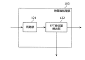
- FIG. 4 is a block diagram illustrating the configuration of the time axis processing unit 103 according to the first embodiment.
- FIG. 5 is a block diagram showing a configuration of interference wave power estimation section 104 according to Embodiment 1.
- FIG. 6 is a block diagram illustrating the configuration of the reliability estimation unit 108 according to the first embodiment.
- FIG. 1 is a block diagram illustrating a configuration of a receiving apparatus according to Embodiment 1.
- FIG. 2 is a block diagram illustrating the configuration of the demodulation unit 11 according to the first embodiment.
- FIG. 3A is a block diagram
- FIG. 7 is a block diagram illustrating a configuration of a receiving apparatus according to the second embodiment.
- FIG. 8 is a block diagram illustrating a configuration of demodulator 21 according to the second embodiment.
- FIG. 9 is a block diagram illustrating the configuration of the jamming wave detection unit 202 according to the second embodiment.
- FIG. 10 is a block diagram illustrating a configuration of interference wave power estimation unit 204 according to Embodiment 2.
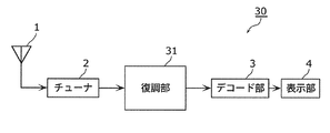
- FIG. 11 is a block diagram illustrating a configuration of a receiving apparatus according to the third embodiment.
- FIG. 12 is a block diagram illustrating a configuration of demodulation section 31 according to the third embodiment.
- FIG. 13 is a block diagram showing the configuration of interference wave power estimation section 304 according to Embodiment 3.
- FIG. 14A is a schematic diagram showing transition of CNR accompanying interpolation processing in transmission path estimation.
- FIG. 14B is a block diagram illustrating an example of the configuration of the transmission path estimation unit 106.
- FIG. 15 is a block diagram illustrating a receiving apparatus according to the fourth embodiment.
- FIG. 16 is a block diagram illustrating a configuration of demodulator 41 according to the fourth embodiment.
- FIG. 17 is a block diagram showing a configuration of reliability estimation section 408 according to the fourth embodiment.
- FIG. 18 is a schematic diagram showing a DVB-T2 frame structure in the DVB-T2 system.
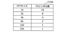
- FIG. 19 is a diagram illustrating the relationship between the FFT size and the number of P2 symbols.
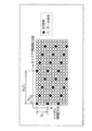
- FIG. 20 is a schematic diagram showing a transmission format (carrier arrangement) in the DVB-T2 system.
- FIG. 21 is a schematic diagram illustrating definitions of a carrier interval and a symbol interval in which an SP signal exists.
- FIG. 22 is a diagram illustrating a carrier interval and a symbol interval in each pilot (SP) pattern.
- FIG. 23 is a diagram showing FFT sizes, CP groups used, and values used for modulo arithmetic.
- FIG. 24 is a diagram illustrating CP group values (CP_g1, CP_g2, CP_g3) for pilot patterns.
- FIG. 25 is a diagram illustrating a CP group value (CP_g4) for a pilot pattern.
- FIG. 26 is a diagram illustrating a CP group value (CP_g5) for a pilot pattern.
- FIG. 27 is a diagram illustrating a CP group value (CP_g6) for a pilot pattern.
- FIG. 28 is a diagram illustrating a CP carrier position added in the extended mode.
- FIG. 29 is a schematic diagram showing the arrangement of pilot signals in each symbol.
- FIG. 30 is a schematic diagram showing a general DVB-T2 receiving apparatus.
- the OFDM method is a method of transmitting a plurality of narrowband digital modulation signals by frequency multiplexing using a plurality of subcarriers orthogonal to each other, and is therefore a transmission method with excellent frequency utilization efficiency.
- one symbol period is composed of an effective symbol period and a guard interval period, and a part of the signal of the effective symbol period is copied and inserted into the guard interval period so as to have periodicity within the symbol. . For this reason, it is possible to reduce the influence of inter-symbol interference caused by multipath interference, and it has excellent resistance to multipath interference.
- FIG. 18 shows a DVB-T2 frame configuration in the DVB-T2 system.
- the DVB-T2 frame is composed of a P1 symbol, a P2 symbol, and a data symbol.
- FFT Fast Fourier Transform
- MISO Multi-Input-Single-Output
- SISO SISO
- FFT size of P2 symbol and data symbol (3) Information including whether FEF (Future Extension Frames) is included.
- the same FFT size as the data symbol is used for the P2 symbol, and equally spaced pilots are inserted.
- the FFT size is 32K and in the SISO mode, there is a P2 pilot every 6 subcarriers.
- the P2 symbol is added with all transmission parameter information necessary for reception, such as a pilot pattern of data symbols, a carrier extension mode (either Extended mode or Normal mode), the number of symbols per frame, a modulation method, etc. Yes. Note that the number of symbols of the P2 symbol is set for each FFT size of the P2 symbol, as shown in Table T190 of FIG.
- Fig. 20 shows the DVB-T2 transmission format.
- the horizontal axis represents the OFDM carrier (frequency) direction
- the vertical axis represents the OFDM symbol (time) direction.
- SP scattered Pilot
- SP scattered Pilot
- a CP Continuous Pilot
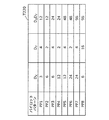
- the carrier interval and the symbol interval at the carrier position where the SP signal exists are defined as Dx and Dy, respectively, the insertion interval Dy in the symbol direction and the insertion in the carrier direction in each SP pattern from PP1 to PP8
- the intervals (Dx ⁇ Dy) are as shown in Table T220 shown in FIG.
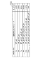
- the insertion subcarrier position of the CP signal is determined by the FFT size and the SP pattern.
- FIG. 23 represents the CP signal position in T230 shown in FIG. 23 and T240, T250, T260, T270, and T280 shown in FIGS.
- FIG. 23 shows which group is used depending on the FFT size in the groups CP_g1 to CP_g6 shown in FIGS.
- the value obtained by performing the modulo operation (residue operation) of the values shown in FIGS. 24 to 27 by K_mod shown in FIG. 23 indicates the effective subcarrier number in which the CP signal exists.
- the FFT size is 32k
- the modulo operation is not performed, and the values shown in FIGS. 24 to 27 are the effective subcarrier numbers in which the CP signal exists as they are.
- the effective subcarrier number shown in FIG. 28 is added.
- the values in FIG. 28 need not be modulo-calculated.
- the CP signal is continuously inserted in the time direction, there are exceptionally symbols that do not have a CP signal. For example, there is no CP signal in the P2 symbol and the Frame Close symbol.
- the transmission format is SISO, either the normal symbol or the Frame Close symbol is defined as the final symbol of the frame according to the combination of the guard interval and the pilot pattern.
- the transmission format is MISO, Frame Close symbols are defined except for PP8.
- FIG. 29 A schematic diagram of a transmission format including a P2 symbol and a Frame Close symbol is shown in FIG.
- the Frame Close (FC) symbol a lot of pilots are inserted as shown in FIG. 29 with respect to a normal data symbol.
- FC Framework Close
- FIG. 30 shows an example of a simplified block diagram of a conventional DVB-T2 reception configuration.
- the conventional DVB-T2 reception configuration includes an A / D conversion unit 1002, a time axis processing unit 1003, an FFT unit 1004, a transmission path estimation unit 1005, and an equalization unit 1006.
- the A / D converter 1002 demodulates the P1 symbol from the A / D (analog-digital) converted signal.
- the time axis processing unit 1003 synchronizes the carrier frequency and the sampling frequency with respect to the P2 symbol and the data symbol.
- the FFT unit 1004 performs FFT to convert the signal into a frequency axis signal.
- the transmission path estimation unit 1005 estimates the transmission path characteristics based on the SP signal included in the signal after the FFT.
- the equalization unit 1006 performs distortion compensation (equalization) of the signal after FFT.
- the error correction unit 1007 performs error correction and demodulates the data.
- the reliability estimation unit 1008 estimates reliability information at the time of transmission path estimation.
- the estimated reliability information is used for error correction in the error correction unit 1007.
- an LDPC (Low Density Parity Check) code is adopted as an error correction code.
- the decoding of the LDPC code requires reliability information that is information representing the reliability of data for weighting the log likelihood ratio.
- the reliability information is estimated from the signal power estimated for each symbol and the noise power including the influence of thermal noise or jamming waves. In order to improve error correction performance in LDPC decoding, it is a very important factor to accurately generate the reception propagation status as reliability information.
- Patent Document 2 is an example of a technique for evaluating the noise power present in each symbol necessary for reliability information estimation.
- the technology disclosed in Patent Document 2 is a TMCC (Transmission Multiplexing Configuration) inserted continuously in a predetermined subcarrier in a time direction in ISDB-T (Integrated Services Digital Broadcasting-Terrestrial), which is a Japanese terrestrial digital broadcasting system.
- This is a technique for evaluating reception quality using at least one of a control (Control) signal and an AC (Auxiliary Channel) signal.
- the TMCC signal is equalized using the transmission path characteristics obtained by interpolating the transmission path characteristics of the SP signal, and received from an error between the TMCC signal differentially demodulated and a hard-decision signal. Calculate quality.
- an impulse interference environment is one of the reception environments in which it is difficult to reflect the state of the reception transmission path in the reliability information.
- Impulse jamming is an irregular and random level jamming signal that is generated in an impulse shape by turning on / off the power supply of home appliances, or by lighting fixtures and vehicle ignition.
- Patent Document 1 there is a method described in Patent Document 1 as an effective technique for eliminating such a deviation of reliability information in a local symbol and improving accuracy.
- the noise power averaged in the symbol direction is compared with the noise power calculated from the pilot signal or the OFDM out-of-band spectrum, and the noise power in each symbol is a predetermined threshold value. If it exceeds the threshold value, it is determined that there is an impulse disturbance, and the noise power value for each symbol is used for reliability information generation. If the threshold value is not exceeded, it is determined that there is no impulse disturbance, and in the symbol direction.
- the average noise power value is used in the generation of reliability information. With this method, it is possible to correctly determine the noise power even when there is an impulse disturbance or when the noise power is locally increased due to the loss of the signal. The performance of LDPC decoding can be improved.
- Patent Document 1 does not disclose a specific noise power calculation method for each symbol.
- the CP signal exists by using the CP signal instead of the TMCC signal as described above. Noise power can be calculated for the frames to be played.
- CP signals are not arranged in the P2 symbol and the FrameClose symbol. In such a symbol in which no CP signal is arranged, noise power cannot be calculated using the CP signal, and noise power averaged in the symbol direction must be used in that symbol.
- a receiving device is a receiving device including a demodulating unit that demodulates a modulated wave modulated by orthogonal frequency division multiplexing (OFDM), wherein the demodulating unit Has exceeded the threshold when it is detected that the received modulated wave includes an interference wave because the received power of each received modulated wave that is the modulated wave received by the receiving device exceeds the threshold.
- OFDM orthogonal frequency division multiplexing
- An interference wave detection unit that performs a replacement process, which is a process for replacing a received signal with a predetermined value, and an OFDM symbol included in the received modulation wave, which is included in the OFDM symbol based on the number of samples on which the replacement process is performed
- a first interference wave power estimation unit that estimates interference wave power, and the first interference wave power estimation unit estimates the received modulation wave after the interference wave detection unit performs the replacement process.
- demodulating the received modulated wave by performing demodulation processing based on the disturbance power and a demodulated data generator for generating a demodulated data.
- the receiving apparatus transmits the interference wave power included in the OFDM symbol based on the number of samples in which the received power exceeds a predetermined threshold in the OFDM symbol, and is transmitted in the OFDM symbol. It is possible to estimate the interference wave power in units of OFDM symbols without depending on the signal type. As a result, in the demodulation processing, the interference wave power calculated based on the number of samples whose received power exceeds a predetermined threshold can be used as the interference wave power of the OFDM symbol in which no CP signal is arranged. Stable reception is possible even if there is an impulse disturbance or signal loss in an OFDM symbol in which no signal is arranged.
- estimation of interference wave power using the specific signal is performed, as in a method of detecting noise power using a CP signal included in the OFDM symbol. Is possible.
- the demodulated data generation unit has a reliability so that the reliability of the OFDM symbol is lower with respect to the received modulation wave as the interference wave power estimated by the first interference wave power estimation unit is larger.
- An error correction for correcting an error included in the received modulated wave using the reliability information estimated by the reliability estimating unit as the demodulation process for the received modulated wave and a reliability estimating unit that estimates information An error correction unit that generates demodulated data of the received modulated wave may be provided by performing the processing.
- noise power estimation including the estimated interference power can be performed regardless of whether noise estimation in the symbol is possible using a noise power detection method using a CP signal. Since reliability information can be generated, error correction can be performed based on highly accurate reliability information and stable reception is possible even if impulse disturbance or signal loss exists.
- the error correction unit weights the log likelihood ratio in LDPC (Low Density Parity Check) demodulation using the reliability information estimated by the reliability estimation unit as the demodulation processing for the received modulated wave.
- LDPC Low Density Parity Check
- LDPC Low Density Parity Check
- demodulation processing can be performed using highly reliable reliability information.
- demodulation processing can be performed in consideration of input reliability information, and more accurate demodulation processing can be performed by inputting highly accurate reliability information.
- the demodulated data generation unit is based on an FFT window position detection unit that specifies an OFDM symbol start timing included in the received modulated wave, and an OFDM symbol start timing specified by the FFT window position detection unit
- An FFT unit that performs an FFT (Fast Fourier Transform) process on the received modulated wave, and generates demodulated data by performing the demodulation process on the received modulated wave that has been subjected to the FFT process. It is good.
- the interference wave detection unit may perform a process of replacing a received signal exceeding the threshold with 0 which is a predetermined value as the replacement process.
- the interference wave detection unit may perform a process of replacing a received signal that exceeds the threshold with the threshold that is a predetermined value as the replacement.
- the residual jamming power can be reduced, and stable reception becomes possible.
- the demodulator further converts the interference wave power included in the first OFDM symbol included in the received modulation wave to the interference wave power included in the second OFDM symbol different from the first OFDM symbol
- a second interference wave power estimation unit that estimates based on the magnitude of the influence of the interference wave power included in the second OFDM symbol on the first OFDM symbol
- the demodulated data generation unit includes the received modulation wave
- the interference wave power can be calculated using an appropriate interference wave power estimation method selected from a plurality of interference wave power estimation methods for each symbol, and can be used for demodulation processing. Effective demodulation is possible, and stable reception is possible.
- the receiving device receives a DVB-T2 (Digital Video Broadcasting-Terrestrial 2) broadcast wave as the modulated wave
- the demodulated data generation unit has an OFDM symbol having a CP (Continuous Pilot) signal.
- the demodulated data of the received modulated wave may be generated using an OFDM symbol group that is not included as the first OFDM symbol group.
- the jamming power can be calculated even for a symbol that cannot be processed using the CP signal. Therefore, effective demodulation is possible using the interference power, and stable reception is possible.
- the demodulated data generation unit uses an OFDM symbol group including an OFDM symbol having a P2 symbol or an FC (Frame Close) symbol in the DVB-T2 system as the first OFDM symbol group, and Demodulated data may be generated.
- the interference power can be calculated even in the P2 symbol or the FC symbol that cannot be processed using the CP signal. It can be used for demodulation processing, and can be effectively demodulated using interference power, and stable reception is possible.
- the demodulated data generation unit further includes a transmission line estimation unit that estimates transmission line characteristics of the modulated wave using the interference power estimated by the first interference wave power estimation unit, and the demodulation The data generation unit may demodulate the received modulated wave and generate demodulated data by performing demodulation processing based on the transmission path characteristic estimated by the transmission path estimation unit.
- the interference power can be calculated regardless of whether noise estimation is possible in the symbol, Effective transmission path estimation is possible based on the interference power, and stable reception is possible.
- the transmission path estimation unit includes a plurality of transmission path interpolation units having different transmission path characteristic interpolation processing methods
- the first interference wave power estimation unit includes the plurality of transmission path estimation interpolation units.
- the transmission path estimation unit calculates one of the outputs of the plurality of transmission path estimation interpolation units based on the interference power estimated by the first disturbance wave power estimation unit. , And output as the transmission line characteristics.
- the interference power can be calculated regardless of whether noise estimation is possible for the symbol, Based on the jamming power, an effective interpolation method for channel estimation can be selected, and stable reception is possible.
- the first interference wave power estimation unit may replace the interference wave power included in the OFDM symbol in the received modulation wave with the number of samples in which the replacement processing is performed in the OFDM symbol, and the FFT in the OFDM symbol. It may be calculated using the number of samples and a predetermined coefficient.
- the interference power can be accurately calculated based on the number of samples exceeding the predetermined threshold included in the OFDM symbol period, the number of FFT samples, and the coefficient related to the predetermined constant, and the effect can be obtained using the interference power. Demodulation is possible, and stable reception is possible.
- the demodulated data generation unit further includes a front of the third OFDM symbol by interpolation using a transmission path characteristic calculated using a pilot signal included in the third OFDM symbol included in the received modulated wave.
- a transmission path estimation unit that estimates transmission path characteristics of each carrier included in the fourth OFDM symbol arranged behind the transmission path characteristics estimated by the transmission path estimation unit, and a signal of the fourth OFDM symbol
- an equalization unit that performs an equalization process, and an error using reliability information that represents the reliability of the signal corrected by the equalization unit with respect to the signal corrected by the equalization unit
- the interference power can be calculated regardless of whether noise estimation is possible in the symbol, Based on the interference power, it is possible to effectively estimate the transmission path of another OFDM symbol, and stable reception is possible.
- An integrated circuit is an integrated circuit including a demodulation unit that demodulates a modulated wave modulated by orthogonal frequency division multiplexing (OFDM), and the demodulation unit is received by the reception device.
- a demodulation unit that demodulates a modulated wave modulated by orthogonal frequency division multiplexing (OFDM)
- the demodulation unit is received by the reception device.
- the received power for each sample of the received modulated wave that is the modulated wave exceeds the threshold value, it is detected that the received modulated wave includes an interference wave, and the received signal that exceeds the threshold value is replaced with a predetermined value.
- An interference wave detection unit that performs a replacement process, and a process for estimating the interference wave power included in the OFDM symbol based on the number of samples subjected to the replacement process in the OFDM symbol included in the received modulated wave.
- One interference wave power estimation unit and the interference wave detection unit based on the interference wave power estimated by the first interference wave power estimation unit for the received modulation wave after the interference wave detection unit performs the replacement process. And demodulating the received modulated wave by performing demodulation processing and a demodulated data generator for generating a demodulated data.
- the integrated circuit has the same effect as the receiving device.
- a receiving method including a demodulating step of demodulating a modulated wave modulated by orthogonal frequency division multiplexing (OFDM), wherein the receiving in the receiving method is received in the demodulating step.
- OFDM orthogonal frequency division multiplexing
- An interference wave detection step for performing a replacement process which is a replacement process, and an interference wave power included in the OFDM symbol based on the number of samples subjected to the replacement process in the OFDM symbol included in the received modulation wave
- a demodulated data generation step of generating demodulated data by demodulating the received modulated wave by performing demodulation process based on the disturbance power estimated by one disturbance power estimation step.
- the receiving method has the same effect as the receiving device.
- a program that is an aspect of the present invention causes a computer to execute the above receiving method.
- Embodiment 1 of a receiving device which is one embodiment of the present invention will be described with reference to FIGS.
- the DVB-T2 system which is the second generation European digital terrestrial broadcasting standard, will be described as an example.
- FIG. 1 is a block diagram showing a receiving device 10 according to Embodiment 1 of the present invention.
- the receiving device 10 includes an antenna 1, a tuner 2, a demodulation unit 11, a decoding unit 3, and a display unit 4.
- the antenna 1 receives a modulated wave modulated by orthogonal frequency division multiplexing (OFDM).
- OFDM orthogonal frequency division multiplexing
- An example of a modulated wave modulated by orthogonal frequency division multiplexing (OFDM) is a DVB-T2 broadcast wave.
- Tuner 2 selects a received signal of a desired reception channel from the modulated wave received by antenna 1.
- the demodulator 11 demodulates the received analog signal selected by the tuner 2.
- the decoding unit 3 is an H.264 demodulated by the demodulation unit 11. A signal compressed by H.264 or the like is decoded.
- the display unit 4 outputs the video / audio decoded by the decoding unit 3.
- FIG. 2 is a block diagram illustrating the configuration of the demodulation unit 11 according to the first embodiment.
- the demodulation unit 11 includes an A / D conversion unit 101, an interference wave detection unit 102, an interference wave power estimation unit 104, and a demodulation data generation unit 12.
- the demodulated data generation unit 12 includes a time axis processing unit 103, an FFT unit 105, a transmission path estimation unit 106, an equalization unit 107, a reliability estimation unit 108, and an error correction unit 109.
- the A / D conversion unit 101 converts the output signal of the tuner 2 from an analog signal to a digital signal and outputs it to the interference wave detection unit 102.
- the interference wave detection unit 102 detects an interference wave included in the reception signal converted into a digital signal by the A / D conversion unit 101, outputs the detection result to the interference wave power estimation unit 104, and detects the detected interference wave.
- the received signal (sample) including is converted into a predetermined value and output to the time axis processing unit 103. Specific processing will be described later.
- the time axis processing unit 103 determines the FFT processing start time position (hereinafter referred to as the FFT window position) in the OFDM symbol period for the output signal of the interference wave detection unit 102, outputs the signal to the FFT unit 105, and the interference signal.
- the FFT window position information is output to the wave power estimation unit 104.
- the interference wave power estimation unit 104 estimates the interference power using the received signal subjected to the interference wave processing by the interference wave detection unit 102 and the FFT window position information determined from the time axis processing unit 103.
- the interference wave power estimation unit 104 corresponds to a first interference wave power estimation unit. Specific processing of the interference wave power estimation unit 104 will be described later.
- the FFT unit 105 performs Fourier transform on the output signal of the time axis processing unit 103 based on the FFT window position signal to convert the signal into a frequency axis signal, and outputs the signal to the transmission path estimation unit 106 and the equalization unit 107.
- the transmission path estimation unit 106 performs interpolation processing on the transmission path characteristics obtained by dividing the SP signal included in the FFT-transformed signal by the known SP signal, so that the transmission path characteristics of all subcarriers are obtained. And the estimated channel characteristics are output to the equalization unit 107 and the reliability estimation unit 108.
- the equalization unit 107 corrects the phase and amplitude distortion received on the transmission path by using the transmission path characteristics estimated by the transmission path estimation unit 106 for the output signal of the FFT unit 105.
- the reliability estimation unit 108 obtains noise power using the channel estimation value estimated by the channel estimation unit 106 and the jamming power estimated by the jamming wave power estimation unit 104, and from this noise power, the error correction unit The reliability information used in 109 is generated.
- the error correction unit 109 corrects the error using the reliability information estimated by the reliability estimation unit 108 for the signal corrected by the equalization unit 107.
- FIG. 3A shows a configuration diagram of the interference wave detection unit 102.
- FIG. 3B shows an example of the interference wave detection signal.
- the interference wave detection unit 102 includes an interference wave sample detection unit 111 and a mask processing unit 112.
- the interference wave sample detection unit 111 compares the received signal ((a) in FIG. 3B) converted into a digital signal by the A / D conversion unit 101 with a predetermined threshold, and outputs a signal indicating a sample position at a level exceeding the threshold. A signal indicating the sample position is output to the mask processing unit 112 along with the received signal.
- Interference Exist 0 (no interference wave) is output.
- the fact that the received signal level exceeds the threshold includes cases where the sign is on both the plus side and the minus side. That is, if the threshold T h is greater than 0, and that the positive (greater than 0) the received signal level is greater than the threshold T h, negative (less than zero) the received signal level is negative threshold (-T h ) smaller than.
- FIG. 4 shows the configuration of the time axis processing unit 103.
- the time axis processing unit 103 includes a synchronization unit 121 and an FFT window position detection unit 122.
- the synchronization unit 121 frequency-converts the output signal of the interference wave detection unit 102 into a baseband signal, establishes synchronization between the carrier frequency and the sampling frequency, and outputs it to the FFT window position detection unit 122.
- the FFT window position detection unit 122 determines the FFT window position for the OFDM symbol for Fourier transform of the time axis signal, and outputs the FFT window position to the FFT unit 105 and the interference wave power estimation unit 104.
- FIG. 5 shows a configuration diagram of the interference wave power estimation unit 104.
- the jamming wave power estimation unit 104 includes a jamming wave sample number counting unit 131 and a jamming power conversion unit 132.
- the interference wave sample number counting unit 131 uses the FFT window position information detected by the FFT window position detection unit 122 for the interference wave detection signal detected by the interference wave detection unit 102 to perform an FFT process on the OFDM symbol section.
- the included number of samples determined as “having interference” is output to the interference power conversion unit 132.
- the jamming power conversion unit 132 estimates the jamming power existing in the OFDM symbol by using the number of samples having “jamming wave” included in the OFDM symbol section counted by the jamming wave sample number counting unit 131 to estimate reliability. To the unit 108. Detailed operation of each part will be described in order.
- the interference wave detection unit 102 Since the interference wave detection unit 102 performs a mask process for replacing the received signal level with 0 for the sample having “interference wave”, the number of interference wave samples increases due to the loss of the OFDM signal. Equal to the amount. For this reason, when the OFDM signal power is set to P OFDM , the signal level of each sample of the OFDM signal is P OFDM / N FFT . Therefore, based on the number of samples N I "with disturbance" included in the OFDM symbol, when the amount of noise increases the OFDM symbol and I Mask, I Mask can be expressed by Equation (1).
- the interference power conversion unit 132 estimates the amount of noise that increases in each OFDM symbol using the conversion formula (Equation 1) and outputs the estimated noise amount to the reliability estimation unit 108, thereby improving the accuracy of the reliability information and receiving performance. To improve.
- FIG. 6 shows a configuration diagram of the reliability estimation unit 108.
- the reliability estimation unit 108 illustrated in FIG. 6 includes a noise estimation unit 141, an interference power addition unit 142, and a reliability information conversion unit 143.
- the noise estimation unit 141 averages the noise power for the OFDM symbol based on the received CP signal from the FFT signal, the transmission path characteristic estimated by the transmission path estimation unit 106, and the known CP signal. Estimate the value (inter-symbol average noise power).
- the jamming power adding unit 142 adds the jamming power estimated by the jamming wave power estimation unit 104 to the estimated inter-symbol average noise power, and outputs the noise power for each symbol in consideration of the jamming wave effect.
- the reliability information conversion unit 143 uses the OFDM signal power estimated by the transmission path estimation unit 106 and based on the transmission path characteristics, and the noise power calculated by the interference power addition unit 142 to use the reliability for LDPC decoding. Information is estimated and output to the error correction unit 109 to perform effective error correction.
- the structure which replaced the TMCC signal with CP signal in patent document 1 for example is used.
- the known CP signal X CP is compared with the received signal Y CP equalized by the transmission path characteristic H CP obtained by the transmission path estimation by interpolation of the SP signal, and the error amount is compared with the CP signal.
- the interference wave power estimation unit 104 may perform sample timing processing on the interference wave detection signal based on rate conversion. Further, based on the signal after the rate conversion, the interference detection and the processing for the interference detection sample described in the interference wave detection unit 102 (processing to replace with 0) may be performed. In that case, it is not necessary for the interference detection signal to consider the effect of rate conversion.
- the mask processing unit 112 replaces 0 with the signal detected by the interference wave sample detection unit 111. However, the sample exceeding the threshold is replaced with 0, and the detection signal is output. As a result, batch processing may be performed.
- the reliability information conversion unit 143 may convert reliability information using information other than noise power and signal power. For example, the reliability information according to the frequency variation can be estimated by using the frequency variation component generated with the Doppler frequency.
- the number of samples included in the OFDM symbol calculated by the interference wave sample number counting unit 131 indicates the amount of noise that locally increases due to the loss of the OFDM signal in that symbol. Therefore, according to the number of jamming wave samples, it may be used as a signal in which jamming waves exist in various blocks. For example, in the calculation of the average noise amount between symbols in the noise estimation unit 141, the noise amount of symbols exceeding a predetermined number of interference wave samples may not be included in the average process.
- the receiving apparatus uses the interference wave power included in the OFDM symbol as the number of samples in which the received power exceeds a predetermined threshold in the OFDM symbol.
- the interference wave power can be estimated for each OFDM symbol without depending on the signal type transmitted in the OFDM symbol.
- the interference wave power calculated based on the number of samples whose received power exceeds a predetermined threshold can be used as the interference wave power of the OFDM symbol in which no CP signal is arranged. Stable reception is possible even if there is an impulse disturbance or signal loss in an OFDM symbol in which no signal is arranged.
- estimation of interference wave power using the specific signal is performed, as in a method of detecting noise power using a CP signal included in the OFDM symbol. Is possible.
- noise power estimation considering the estimated interference power can be performed regardless of whether noise estimation in the symbol can be performed using a noise power detection method using a CP signal. Therefore, even if impulse disturbance or signal loss exists, error correction can be performed based on highly reliable reliability information, and stable reception is possible.
- LDPC Low Density Parity Check
- demodulation processing can be performed using highly reliable reliability information.
- demodulation processing can be performed in consideration of input reliability information, and more accurate demodulation processing can be performed by inputting highly accurate reliability information.
- the interference power can be calculated regardless of whether noise estimation is possible for the symbol. Based on this, effective transmission path estimation becomes possible, and stable reception becomes possible.
- the interference power can be accurately calculated based on the number of samples exceeding a predetermined threshold included in the OFDM symbol period, the number of FFT samples, and a coefficient related to a predetermined constant, and effective demodulation is performed using the interference power. And stable reception is possible.
- FIGS. 1 to 6 A second embodiment of the receiving apparatus of the present invention will be described with reference to FIGS.
- the same components as those in FIGS. 1 to 6 are denoted by the same reference numerals, and description thereof is omitted.
- FIG. 7 is a block diagram showing the receiving device 20 according to the second embodiment of the present invention
- FIG. 8 is a block diagram showing the configuration of the demodulator 21.
- FIG. 8 differs from FIG. 2 only in the interference wave detection unit 202 and the interference wave power estimation unit 204.
- FIG. 9 shows a configuration diagram of the interference wave detection unit 202.
- the interference wave detection unit 202 includes an interference wave sample detection unit 211 and a clip processing unit 212.
- the interference wave sample detection unit 211 compares the reception signal converted into the digital signal by the A / D conversion unit with a predetermined threshold, and, together with the reception signal, in the same manner as the interference wave sample detection unit 111 of the first embodiment. Outputs wave detection signal.
- the predetermined value may be the same as the threshold value used in the interference wave sample detection unit 211. If the received signal exceeds the minus threshold value, it may be the same as the minus threshold value in this process.
- the interference wave detection signal output from the interference wave detection unit 202 is output to the interference wave power estimation unit 204.
- FIG. 10 is a block diagram showing the configuration of the interference wave power estimation unit 204.
- the jamming wave power estimation unit 204 includes a jamming wave sample number counting unit 131 and a jamming power conversion unit 232.
- the interference wave sample number counting unit 131 counts the number of samples having an interference wave included in the OFDM symbol as described in Embodiment 1, and outputs the counted number to the interference power conversion unit 232.
- the interference power conversion unit 232 calculates the interference wave power included in the OFDM signal based on the number of samples with the interference wave calculated by the interference wave sample number counting unit 131.
- the OFDM signal power is P OFDM and the square of the interference clipped value is A Clip ⁇ P OFDM
- the signal level of each sample of the OFDM signal is P OFDM / N FFT
- the clipped interference power The signal level is A Clip ⁇ P OFDM / N FFT . Therefore, the interference wave power I Clip when the interference wave is clipped can be expressed by (Equation 2).
- the jamming power adding unit 142 in the reliability estimation unit 108 takes into account the jamming wave component included in the symbol, and the reliability estimation unit increases the accuracy of the reliability information as in the first embodiment. By using it for LDPC decoding, stable reception becomes possible.
- the interference wave power estimation unit may perform sample timing processing on the interference wave detection signal based on rate conversion. Further, based on the signal after the rate conversion, the interference detection and the processing for the interference detection sample described in the interference wave detection unit 202 (processing to replace with a predetermined value) may be performed. In that case, it is not necessary for the interference detection signal to consider the effect of rate conversion.
- the clip processing unit 212 replaces the sample with a predetermined value based on the signal detected by the interference wave sample detection unit 211. However, the sample exceeding the threshold is replaced with the predetermined value, and the detection signal is output. Alternatively, batch processing may be performed.
- the configuration may be such that the OFDM signal component is subtracted.
- the receiving apparatus by setting a sample in which an interfering wave exists to a predetermined value, residual interference electric power can be reduced and stable reception is possible.
- Embodiment 3 of the receiving apparatus of the present invention will be described with reference to FIGS. 11 to 14A.
- the same components as those in FIGS. 1 to 6 are denoted by the same reference numerals, and description thereof is omitted.
- FIG. 11 is a block diagram showing a receiving device 30 according to the third embodiment of the present invention
- FIG. 12 is a block diagram showing a configuration of the demodulator 31.
- the demodulator 31 shown in FIG. 12 differs from the demodulator 11 of the first embodiment in the configuration of the interference wave power estimator 304.
- FIG. 13 shows a configuration diagram of the interference wave power estimation unit 304.
- the jamming wave power estimation unit 304 includes a jamming wave sample number counting unit 131, a jamming power conversion unit 132, a second jamming power conversion unit 332, and an addition unit 333.
- the interference wave power estimation unit 304 corresponds to a second interference wave power estimation unit.
- the interference wave sample number counting unit 131 is based on the interference wave detection signal detected by the interference wave detection unit 102 and the OFDM symbol position where the FFT detected by the FFT window position detection unit 122 is performed. Then, the number of samples “having jamming” included in the OFDM symbol is counted and output to the jamming power conversion unit 132 and the second jamming power conversion unit 332.
- the interference power conversion unit 132 calculates the interference power included in the received OFDM symbol from the output of the interference wave sample number counting unit 131 as in the first embodiment.
- the present embodiment is different from the first embodiment in that it includes a second interference power conversion unit 332.
- the second interference power conversion unit 332 calculates the interference power generated in the OFDM symbol from the interference wave included in another OFDM symbol.
- the interference wave power generated by the transmission path estimation is estimated in consideration of the influence of the interference wave being diffused to other OFDM symbols corrected by the equalization unit 107 by the interpolation processing in the transmission path estimation.
- the adding unit 333 adds the interference power of the OFDM symbol estimated by the interference power conversion unit 132 and the interference power from other OFDM symbols estimated by the second interference power conversion unit 332, and outputs the sum.
- Transmission path characteristics are estimated by interpolating the transmission path characteristics of SP signals, P2 pilot signals, and FC signals that are dispersed in the time axis (symbol) direction and frequency axis (carrier) direction. It is to obtain road characteristics.
- interpolation there are (A) a method of interpolating in the time axis (symbol) direction and then interpolating in the frequency axis (carrier) direction, and (B) a method of interpolating only in the frequency axis (carrier) direction.
- FIG. 14A shows a case where (A) time axis interpolation and frequency interpolation are used as interpolation processing in transmission path estimation in an impulse interference environment, and (B) frequency axis interpolation only (no time axis interpolation) is used.
- the transition of CNR (Carrier to Noiseratio) of each OFDM symbol after correction by the equalization unit 107 is shown.
- the horizontal axis of the graph indicates the symbol direction (time direction), and the vertical axis indicates the CNR.
- impulse interference occurs at the timing of the star ( ⁇ )
- (B) In the case of only frequency axis interpolation, the CNR deteriorates only with the symbol where the impulse interference has occurred. In this case, since the symbol subjected to the impulse interference is used for the interpolation processing, an interpolation error due to the interference wave occurs, and the CNR deteriorates also in the symbols before and after the impulse interference exists.
- the second interference power conversion unit 332 takes into account the influence of the interference wave due to the transmission path estimation. Therefore, in the case of only (B) frequency axis interpolation, the transmission path in its own symbol. Consider the influence of characteristics as interference power. Further, in the case of (A) time axis interpolation + frequency interpolation, the influence of the symbol with interference and the symbols before and after it are also considered as interference power.
- the interference wave sample number output from the interference wave sample number counting unit 131 is subjected to the same processing as time interpolation, the number of interference samples including the influence of the interference wave by time axis interpolation is estimated, and the interpolation error is calculated. Convert the disturbing power in consideration.
- the influence of the interference wave on the transmission path estimation is different in the two patterns of (A) time axis interpolation + frequency axis interpolation and (B) frequency axis interpolation only. Details of each pattern will be described below.
- NH_TF2sym (i) 1/2 ⁇ ⁇ N I (i) + (1/2) 2 ⁇ (N I (i ⁇ 1) + N I (i + 1)) ⁇ (Equation 3)
- NH_TF4sym (i) 1 ⁇ 4 ⁇ ⁇ N I (i) + (3/4) 2 ⁇ (N I (i ⁇ 1) + N I (i + 1)) + (2/4) 2 ⁇ (N I (i ⁇ 2) + N I (i + 2)) + (1/4) 2 ⁇ (N I (i ⁇ 3) + N I (i + 3)) ⁇ (Formula 4)
- the interference wave sample number N H_F (i) in the transmission path estimation in the i symbol is as follows.
- the adder 333 adds not only the interference power included in the OFDM symbol but also the transmission path by adding the interference power estimated by the interference power section to the interference power estimated by the transmission path estimation error corresponding to each interpolation method.
- the interference power including the influence of the interference wave in the estimation can be considered. Since this interference power can be accurately reflected in the reliability information in the interference power addition unit 142 in the reliability estimation unit 108, highly accurate reliability information can be obtained, and as a result, effective LDPC decoding can be performed. And reception performance can be improved.
- linear interpolation is used as the time axis interpolation, but the present invention is not limited to this, and an arbitrary interpolation method (interpolation coefficient) may be used.
- the interpolation method may be selected based on the calculated interference power in consideration that the influence of the interference power differs depending on the interpolation method and the signal quality is different in the first place.
- the transmission path estimation unit 206 shown in FIG. 14B may be used.
- the transmission path estimation unit 206 includes a first transmission path interpolation unit 106A, a second transmission path interpolation unit 106B, and a selector 106S.
- the first transmission path interpolation unit 106A and the second transmission path interpolation unit 106B estimate different transmission path characteristics.
- the selector 106S selects one of the outputs from the first transmission line interpolation unit 106A and the second transmission line interpolation unit 106B, and outputs the selected transmission line characteristic. In this way, a plurality of transmission path characteristics can be selectively used as reliability information for demodulation processing.
- the interference wave power estimation unit can estimate the interference power corresponding to each interpolation processing method.
- the interference wave power can be calculated using an appropriate interference wave power estimation method selected from a plurality of interference wave power estimation methods for each symbol, and demodulated. It can be used for processing and can be effectively demodulated using the interference wave power, thereby enabling stable reception.
- the interference power can be calculated even for symbols that cannot be processed using the CP signal, and used for demodulation processing. Therefore, effective demodulation is possible using the interference power, and stable reception is possible.
- the interference power can be calculated even in the P2 symbol or the FC symbol that cannot be processed using the CP signal. It can be used for processing, and can be effectively demodulated using jamming power, thereby enabling stable reception.
- the interference power can be calculated regardless of whether noise estimation is possible for the symbol. Based on this, it is possible to select an effective interpolation method for channel estimation, and stable reception is possible.
- Embodiment 4 of the receiving apparatus of the present invention will be described.
- the same components as those in FIGS. 1 to 6 are denoted by the same reference numerals, and description thereof is omitted.
- FIG. 15 is a block diagram showing a receiving device 40 according to Embodiment 4 of the present invention
- FIG. 16 is a block diagram showing the configuration of the demodulator 41.
- the demodulator 41 is different from the demodulator 11 shown in Embodiment 1 in terms of addition of interference power in the reliability estimator 408.
- FIG. 17 is a block diagram showing the configuration of the reliability estimation unit 408.
- the reliability estimation unit 408 includes a noise estimation unit 441, an interference power addition unit 442, and a reliability information conversion unit 143.
- the noise estimation unit 441 outputs the noise estimation value for each symbol that is not averaged in the symbol direction to the interference power addition unit 442 together with the symbol average noise estimation value averaged in the symbol direction.
- the jamming power adding unit 442 is different from the jamming power adding unit 142 of the first embodiment in that it selects whether or not to add the jamming power estimated by the jamming power estimation unit 104 according to the symbol to be processed. .
- the current symbol type P1 symbol, P2 symbol, data symbol, or FC
- Symbol is output by adding interference power to the symbol average noise estimate for a specific symbol, and without adding interference power to the noise estimate for each symbol that is not averaged in the symbol direction, except for a specific symbol. Output.
- a specific example in the DVB-T2 system is shown below.
- the P2 symbol and the FC symbol do not include a CP signal, noise power estimation using the CP signal cannot be performed for those symbols.
- noise power can be estimated using a CP signal for each symbol. Therefore, the interference power is added to the noise estimation value averaged in the symbol direction in the P2 symbol or the FC symbol where the noise power cannot be estimated using the CP signal for each symbol, and is output. Further, other symbols are output without adding interference power to the noise estimation value for each symbol that is not averaged in the symbol direction.
- the noise estimation value calculated for each symbol is used for symbols that can be estimated for each symbol, and the interference power is added to the average noise estimation value for symbols that cannot be estimated.
- the amount of noise can be accurately reflected in the reliability information. Therefore, highly accurate reliability information can be obtained.
- effective LDPC decoding can be performed, and reception performance can be improved.
- the noise estimation value for each symbol that is not averaged in the symbol direction is used.
- the present invention is not limited to this. It is also possible to select the estimated noise value. For example, when the noise estimation value for each symbol is large compared with each other, the noise estimation value for each symbol may be used, and otherwise, the average noise estimation value may be used.
- the number of interference samples estimated by the interference wave power estimation unit 104 is a predetermined number or more, a noise estimation value for each symbol may be used, and otherwise, an average noise estimation value may be used.
- the present embodiment is configured to select whether or not the interference power can be added according to the symbol type, as compared with the first embodiment, the present embodiment is applied to the second and third embodiments. Also good.
- the receiving apparatus of one aspect of the present invention it is possible to estimate noise in a symbol by calculating the interference power based on the number of samples exceeding a predetermined threshold included in the OFDM symbol period. Regardless of whether or not the interference power can be calculated, the transmission path estimation of other OFDM symbols can be performed effectively based on the interference power, and stable reception is possible.
- the reliability of the sex information is lowered to a predetermined value compared to other symbols. For example, when the number of jamming wave samples included in the OFDM symbol is equal to or greater than a predetermined threshold, the reliability estimation value may be reduced to half. In this case, since detailed interference power calculation is unnecessary, the circuit scale can be reduced.
- each component of the OFDM receiver in Embodiments 1 to 4 may be realized by an LSI that is an integrated circuit. At this time, each component may be individually made into one chip, or may be made into one chip so as to include a part or all of them.
- LSI here, it may be referred to as IC, system LSI, super LSI, or ultra LSI depending on the degree of integration.
- the method of circuit integration is not limited to LSI, and implementation with a dedicated circuit or a general-purpose processor is also possible. Further, the method of circuit integration is not limited to LSI, but may be realized by a dedicated circuit or a general-purpose processor.
- An FPGA Field Programmable Gate Array
- a reconfigurable processor capable of reconfiguring connection and setting of circuit cells inside the LSI may be used. Furthermore, if integrated circuit technology comes out to replace LSI's as a result of the advancement of semiconductor technology or a derivative other technology, it is naturally also possible to carry out function block integration using this technology. Possible applications include biotechnology.
- the receiving program for example, a CPU (Central Processing Unit) reads and executes the program stored in the memory.
- the program may be stored in a recording medium and distributed.
- the receiving apparatuses according to the first to fourth embodiments may be realized by using a receiving method that performs at least a part of the described receiving process.
- Embodiments 1 to 4 may be realized by combining any receiving device, a receiving method, an integrated circuit, or a program that performs a part of the reception processing that realizes Embodiments 1 to 4.
- a part of the configuration of the receiving device described in each of the above embodiments is realized by the receiving device or the integrated circuit, and an operation procedure performed by the configuration excluding the part is described in the receiving program. It may be realized by reading out and executing the program stored in.
- Embodiments 1 to 4 refer to the DVB-T2 system
- the present invention is not limited to this. Similar to DVB-T2, it can be applied in the field of OFDM communication in which improvement in noise power estimation accuracy in accordance with propagation path changes caused by interference waves is effective.
- each component may be configured by dedicated hardware or may be realized by executing a software program suitable for each component.
- Each component may be realized by a program execution unit such as a CPU or a processor reading and executing a software program recorded on a recording medium such as a hard disk or a semiconductor memory.
- the software that realizes the image decoding apparatus of each of the above embodiments is the following program.
- this program is a reception method including a demodulation step of demodulating a modulated wave modulated by orthogonal frequency division multiplexing (OFDM) to a computer, wherein the modulation received in the reception method in the demodulation step.
- OFDM orthogonal frequency division multiplexing
- the receiving apparatus detects the presence or absence of an interfering wave for each sample in the time axis region, estimates the interfering power based on the number of samples with an interfering wave included in the FFT sample period of the OFDM symbol, and performs LDPC decoding.
- an OFDM receiver that has a function to estimate reliability information to be used based on interference power and requires highly accurate reliability information such as DVB-T2, and in devices in a wide range of fields such as measurement It is beneficial.
Landscapes
- Engineering & Computer Science (AREA)
- Signal Processing (AREA)
- Computer Networks & Wireless Communication (AREA)
- Health & Medical Sciences (AREA)
- Biomedical Technology (AREA)
- General Health & Medical Sciences (AREA)
- Multimedia (AREA)
- Environmental & Geological Engineering (AREA)
- Noise Elimination (AREA)
Abstract
Description
以下、本願発明の実施形態の説明に先立って、本願発明が適用可能なシステムの一例である、OFDM方式を採用するデジタルテレビ放送について図面を参照して説明する。
本願発明の一態様である受信装置の実施の形態1について、図1~図6を参照して説明する。ここでは一例として第二世代欧州地上デジタル放送規格であるDVB-T2方式を例に挙げて説明を行う。
本願発明の受信装置の実施の形態2について、図7~図10を参照して説明する。図1~図6と同じ構成要素は、同じ符号を用い、説明を省略する。
本願発明の受信装置の実施の形態3について、図11~図14Aを参照して説明する。図1~図6と同じ構成要素は、同じ符号を用い、説明を省略する。
DVB-T2方式では、SPパターンが8種類ある。説明を簡単化するために、時間軸方向の直線補間する場合を例にして説明する。時間軸方向のSPキャリア間隔は、(1)2キャリアおき、又は(2)4キャリアおきの2種類が考えられる。よって、時間補間において妨害波の影響が拡散する範囲は、妨害波が検出されたシンボルを中心に、(1)の場合は前後それぞれ1シンボル、(2)の場合は前後それぞれ3シンボルとなる。よって、iシンボルにおける妨害波による伝送路推定誤差を見積もるための妨害波サンプル数(1):NH_TF2sym、及び、(2):NH_TF4symは、それぞれ以下のようになる。
=1/2×{NI(i)+(1/2)2×(NI(i-1)
+NI(i+1))} ・・・(式3)
NH_TF4sym(i)
=1/4×{NI(i)+(3/4)2×(NI(i-1)
+NI(i+1))+(2/4)2×(NI(i-2)+NI(i+2))
+(1/4)2×(NI(i-3)+NI(i+3))} ・・・(式4)
周波数軸補間のみ場合は、妨害波が存在するシンボル前後には影響が拡散しないため、iシンボルにおける伝送路推定における妨害波サンプル数NH_F(i)は、以下のようになる。
IH_TF=(1/ASP)×NH_TF/NFFT×BWT×BWF ・・・(式6)
IH_F=(1/ASP)×NH_F/NFFT×BWF ・・・(式7)
本願発明の受信装置の実施の形態4について説明する。図1~図6と同じ構成要素は、同じ符号を用い、説明を省略する。
2 チューナ
3 デコード部
4 表示部
10、20、30、40 受信装置
11、21、31、41 復調部
12、22、32、42 復調データ生成部
101 A/D変換部
102 妨害波検出部
103 時間軸処理部
104 妨害波電力推定部
105 FFT部
106 伝送路推定部
107 等化部
108 信頼性推定部
109 誤り訂正部
111 妨害波サンプル検出部
112 マスク処理部
121 同期部
122 FFT窓位置検出部
131 妨害波サンプル数カウント部
132 妨害電力換算部
141 雑音推定部
142 妨害電力加算部
143 信頼性情報換算部
202 妨害波検出部
204 妨害波電力推定部
211 妨害波サンプル検出部
212 クリップ処理部
232 妨害電力換算部
304 妨害波電力推定部
332 第二妨害電力換算部
333 加算部
408 信頼性推定部
441 雑音推定部
442 妨害電力加算部
1002 A/D変換部
1003 時間軸処理部
1004 FFT部
1005 伝送路推定部
1006 等化部
1007 誤り訂正部
1008 信頼性推定部
Claims (16)
- 直交周波数分割多重方式(OFDM)で変調された変調波を復調する復調部を備える受信装置であって、
前記復調部は、
前記受信装置が受信した前記変調波である受信変調波のサンプルごとの受信電力が閾値を超えることで、前記受信変調波が妨害波を含むことを検出した場合に、前記閾値を超えた受信信号を所定値に置き換える処理である置換処理を行う妨害波検出部と、
前記受信変調波に含まれるOFDMシンボルにおいて、前記置換処理が行われたサンプル数に基づいて、前記OFDMシンボルに含まれる妨害波電力を推定する第一妨害波電力推定部と、
前記妨害波検出部が前記置換処理を行った後の前記受信変調波に対して、前記第一妨害波電力推定部が推定した前記妨害波電力に基づいた復調処理を行うことで前記受信変調波を復調し復調データを生成する復調データ生成部とを備える
受信装置。 - 前記復調データ生成部は、
前記受信変調波に対して、前記第一妨害波電力推定部が推定した前記妨害波電力が大きいほど前記OFDMシンボルの信頼性が低くなるように信頼性情報を推定する信頼性推定部と、
前記受信変調波に対する前記復調処理として、前記信頼性推定部が推定した信頼性情報を用いて、前記受信変調波に含まれる誤りを訂正するための誤り訂正処理を行うことで、前記受信変調波の復調データを生成する誤り訂正部とを有する
請求項1に記載の受信装置。 - 前記誤り訂正部は、
前記受信変調波に対する前記復調処理として、前記信頼性推定部が推定した信頼性情報を用いて、LDPC(Low Density Parity Check)復調における対数尤度比の重み付け処理を行うことで、前記受信変調波の復調データを生成する
請求項2に記載の受信装置。 - 前記復調データ生成部は、
前記受信変調波に含まれるOFDMシンボルの開始タイミングを特定するFFT窓位置検出部と、
前記FFT窓位置検出部が特定した前記OFDMシンボルの開始タイミングに基づいて、前記受信変調波に対しFFT(Fast Fourier Transform)処理を施すFFT部とを有し、
前記FFT処理が施された前記受信変調波に対して前記復調処理を行うことで復調データを生成する
請求項1~3のいずれか1項に記載の受信装置。 - 前記妨害波検出部は、
前記置換処理として、前記閾値を超えた受信信号を所定値である0に置き換える処理を行う
請求項1~4のいずれか1項に記載の受信装置。 - 前記妨害波検出部は、
前記置換処理として、前記閾値を超えた受信信号を所定値である前記閾値に置き換える処理を行う
請求項1~4のいずれか1項に記載の受信装置。 - 前記復調部は、さらに、
前記受信変調波に含まれる第一OFDMシンボルに含まれる妨害波電力を、前記第一OFDMシンボルと異なる第二OFDMシンボルに含まれる妨害波電力と、前記第二OFDMシンボルに含まれる前記妨害波電力が前記第一OFDMシンボルに及ぼす影響の大きさとに基づいて推定する第二妨害波電力推定部を備え、
前記復調データ生成部は、
前記受信変調波に含まれる少なくとも1つのOFDMシンボルからなる第一OFDMシンボル群に対して前記第一妨害波電力推定部が推定した前記妨害波電力を考慮した誤り訂正を含む復調処理を行うことで、前記受信変調波の復調データを生成し、前記受信変調波に含まれるOFDMシンボルのうち第一OFDMシンボル群に含まれないOFDMシンボルからなる第二OFDMシンボル群に対して前記第二妨害波電力推定部が推定した前記妨害波電力を考慮した誤り訂正を含む復調処理を行うことで、前記受信変調波の復調データを生成する
請求項1~6のいずれか1項に記載の受信装置。 - 前記受信装置は、
DVB-T2(Digital Video Broadcasting -Terrestrial 2)方式の放送波を前記変調波として受信し、
前記復調データ生成部は、
CP(Continual Pilot)信号を有するOFDMシンボルが含まれていないOFDMシンボル群を前記第一OFDMシンボル群として用いて、前記受信変調波の復調データを生成する
請求項7に記載の受信装置。 - 前記復調データ生成部は、
DVB-T2方式におけるP2シンボルまたはFC(Frame Close)シンボルを有するOFDMシンボルを含むOFDMシンボル群を前記第一OFDMシンボル群として用いて、前記受信変調波の復調データを生成する
請求項7または請求項8に記載の受信装置。 - 前記復調データ生成部は、さらに、
前記第一妨害波電力推定部が推定した妨害電力を用いて、前記変調波の伝送路特性を推定する伝送路推定部を有し、
前記復調データ生成部は、前記伝送路推定部が推定した伝送路特性に基づいた復調処理を行うことで前記受信変調波を復調し復調データを生成する
請求項1~9のいずれか1項に記載の受信装置。 - 前記伝送路推定部は、
前記伝送路特性の補間処理方法が互いに異なる複数の伝送路補間部を有し、
前記第一妨害波電力推定部は、
前記複数の伝送路推定補間部のそれぞれに対応する妨害電力を推定し、
前記伝送路推定部は、
前記第一妨害波電力推定部が推定した前記妨害電力に基づいて、前記複数の伝送路推定補間部の出力のいずれかを、前記伝送路特性として出力する
請求項10に記載の受信装置。 - 前記第一妨害波電力推定部は、
前記受信変調波に前記OFDMシンボルに含まれる妨害波電力を、前記OFDMシンボルにおいて前記置換処理が行われたサンプル数と、前記OFDMシンボルにおけるFFTサンプル数と、所定の係数とを用いて算出する
請求項1~11のいずれか1項に記載の受信装置。 - 前記復調データ生成部は、さらに、
前記受信変調波に含まれる第三OFDMシンボルに含まれるパイロット信号を用いて算出した伝送路特性を用いた補間により、前記第三OFDMシンボルの前方または後方に配置された第四OFDMシンボルに含まれる各キャリアの伝送路特性を推定する伝送路推定部と、
前記伝送路推定部が推定した伝送路特性を用いて、前記第四OFDMシンボルの信号を補正する処理である等化処理を行う等化部と、
前記等化部で補正された信号に対して、前記等化部で補正された信号の信頼性を表す信頼性情報を用いて誤り訂正を行う誤り訂正部と、
前記妨害波電力推定部で推定した前記第三OFDMシンボルの妨害波電力を用いて、前記第四OFDMシンボルに含まれる信号の信頼性情報を推定する信頼性情報推定部とを有する
請求項1に記載の受信装置。 - 直交周波数分割多重方式(OFDM)で変調された変調波を復調する復調部を備える集積回路であって、
前記復調部は、
前記受信装置が受信した前記変調波である受信変調波のサンプルごとの受信電力が閾値を超えることで、前記受信変調波が妨害波を含むことを検出した場合に、前記閾値を超えた受信信号を所定値に置き換える処理である置換処理を行う妨害波検出部と、
前記受信変調波に含まれるOFDMシンボルにおいて、前記置換処理が行われたサンプル数に基づいて、前記OFDMシンボルに含まれる妨害波電力を推定する第一妨害波電力推定部と、
前記妨害波検出部が前記置換処理を行った後の前記受信変調波に対して、前記第一妨害波電力推定部が推定した前記妨害波電力に基づいた復調処理を行うことで前記受信変調波を復調し復調データを生成する復調データ生成部とを備える
集積回路。 - 直交周波数分割多重方式(OFDM)で変調された変調波を復調する復調ステップを含む受信方法であって、
前記復調ステップにおいて、
前記受信方法において受信された前記変調波である受信変調波のサンプルごとの受信電力が閾値を超えることで、前記受信変調波が妨害波を含むことを検出した場合に、前記閾値を超えた受信信号を所定値に置き換える処理である置換処理を行う妨害波検出ステップと、
前記受信変調波に含まれるOFDMシンボルにおいて、前記置換処理が行われたサンプル数に基づいて、前記OFDMシンボルに含まれる妨害波電力を推定する第一妨害波電力推定ステップと、
前記妨害波検出ステップにおいて前記置換処理が行われた後の前記受信変調波に対して、前記第一妨害波電力推定ステップにより推定された前記妨害波電力に基づいた復調処理を行うことで前記受信変調波を復調し復調データを生成する復調データ生成ステップとを含む
受信方法。 - 請求項15に記載の受信方法をコンピュータに実行させるためのプログラム。
Priority Applications (4)
| Application Number | Priority Date | Filing Date | Title |
|---|---|---|---|
| CN201280001991.4A CN103004164B (zh) | 2011-05-18 | 2012-05-17 | 接收装置、集成电路、接收方法及程序 |
| JP2012532184A JP5358738B2 (ja) | 2011-05-18 | 2012-05-17 | 受信装置、集積回路、受信方法、及び、プログラム |
| EP12785178.0A EP2712101B1 (en) | 2011-05-18 | 2012-05-17 | Reception device, integrated circuit, reception method, and program |
| US13/809,921 US8731037B2 (en) | 2011-05-18 | 2012-05-17 | Receiver, integrated circuit, receiving method, and program |
Applications Claiming Priority (2)
| Application Number | Priority Date | Filing Date | Title |
|---|---|---|---|
| JP2011-111893 | 2011-05-18 | ||
| JP2011111893 | 2011-05-18 |
Publications (1)
| Publication Number | Publication Date |
|---|---|
| WO2012157281A1 true WO2012157281A1 (ja) | 2012-11-22 |
Family
ID=47176630
Family Applications (1)
| Application Number | Title | Priority Date | Filing Date |
|---|---|---|---|
| PCT/JP2012/003254 Ceased WO2012157281A1 (ja) | 2011-05-18 | 2012-05-17 | 受信装置、集積回路、受信方法、及び、プログラム |
Country Status (5)
| Country | Link |
|---|---|
| US (1) | US8731037B2 (ja) |
| EP (1) | EP2712101B1 (ja) |
| JP (1) | JP5358738B2 (ja) |
| CN (1) | CN103004164B (ja) |
| WO (1) | WO2012157281A1 (ja) |
Cited By (4)
| Publication number | Priority date | Publication date | Assignee | Title |
|---|---|---|---|---|
| CN103546797A (zh) * | 2012-07-11 | 2014-01-29 | 扬智电子科技(上海)有限公司 | 信号接收系统及其方法 |
| JP2016526840A (ja) * | 2013-07-05 | 2016-09-05 | エルジー エレクトロニクス インコーポレイティド | 放送信号送信装置、放送信号受信装置、放送信号送信方法及び放送信号受信方法 |
| CN106464640A (zh) * | 2015-03-24 | 2017-02-22 | Lg 电子株式会社 | 发送和接收广播信号的装置和方法 |
| JP2017532821A (ja) * | 2014-08-25 | 2017-11-02 | エレクトロニクス アンド テレコミュニケーションズ リサーチ インスチチュートElectronics And Telecommunications Research Institute | レイヤードディビジョンマルチプレキシングを利用した放送信号フレーム生成装置および放送信号フレーム生成方法 |
Families Citing this family (14)
| Publication number | Priority date | Publication date | Assignee | Title |
|---|---|---|---|---|
| US8588724B2 (en) * | 2009-08-20 | 2013-11-19 | Alfred E. Mann Foundation For Scientific Research | Optimal narrowband interference removal for signals separated in time |
| CN102858004B (zh) * | 2012-09-04 | 2018-03-27 | 中兴通讯股份有限公司 | 一种基站、终端及其功率控制方法 |
| US9680681B2 (en) | 2013-03-04 | 2017-06-13 | Mitsubishi Electric Corporation | Transmission apparatus, reception apparatus, and communication system |
| US9264924B2 (en) * | 2013-03-07 | 2016-02-16 | Cable Television Laboratories, Inc. | Signal noise estimation |
| EP2975790B1 (en) * | 2013-03-13 | 2019-02-20 | Mitsubishi Electric Corporation | Transmission device, reception device and communication system |
| JP6118616B2 (ja) * | 2013-03-29 | 2017-04-19 | 富士通株式会社 | 受信機および同期補正方法 |
| EP3050233B1 (en) * | 2013-09-25 | 2023-06-07 | Nokia Solutions and Networks GmbH & Co. KG | Configuration of channel estimation related parameters |
| EP2928139B1 (en) * | 2014-03-31 | 2020-09-30 | Mitsubishi Electric R&D Centre Europe B.V. | Method and a device for cancelling a narrow band interference in a single carrier signal |
| US9306678B2 (en) * | 2014-04-24 | 2016-04-05 | Comcast Cable Communications, Llc | Data interpretation with noise signal analysis |
| US9497056B2 (en) * | 2014-06-09 | 2016-11-15 | Allen LeRoy Limberg | Conveying metadata by modulation of pilot carriers in COFDM broadcasting |
| TWI575901B (zh) * | 2015-06-17 | 2017-03-21 | 晨星半導體股份有限公司 | 通道效應消除裝置及通道效應消除方法 |
| US10237781B2 (en) * | 2016-02-19 | 2019-03-19 | Zte Corporation | Channel quality estimation for link adaptation within interference limited systems |
| US10420052B2 (en) * | 2016-02-25 | 2019-09-17 | Qualcomm Incorporated | Estimating frequency error with beacon transmissions |
| CN115208493B (zh) * | 2022-06-22 | 2023-10-27 | 上海伽易信息技术有限公司 | 一种基于手持终端的地铁cbtc信号检测方法、系统及装置 |
Citations (3)
| Publication number | Priority date | Publication date | Assignee | Title |
|---|---|---|---|---|
| JP2005333528A (ja) * | 2004-05-21 | 2005-12-02 | Matsushita Electric Ind Co Ltd | 妨害波除去装置 |
| JP3740468B2 (ja) | 2003-01-22 | 2006-02-01 | 株式会社東芝 | Ofdm受信装置及びデータ復調方法 |
| EP2242226A2 (en) | 2009-03-31 | 2010-10-20 | Sony Corporation | Receiver and method of receiving |
Family Cites Families (6)
| Publication number | Priority date | Publication date | Assignee | Title |
|---|---|---|---|---|
| US7418026B2 (en) | 2002-05-09 | 2008-08-26 | Sony United Kingdom Limited | Receiver for a multi-carrier modulated symbol |
| WO2006068186A1 (ja) | 2004-12-21 | 2006-06-29 | Matsushita Electric Industrial Co., Ltd. | Ofdm受信装置 |
| JP4610401B2 (ja) | 2005-04-13 | 2011-01-12 | 株式会社エヌ・ティ・ティ・ドコモ | チャネル推定装置 |
| US7558337B2 (en) * | 2005-08-12 | 2009-07-07 | Ati Technologies, Inc. | Systems, methods, and apparatus for impulse noise mitigation |
| JP4816424B2 (ja) * | 2006-11-21 | 2011-11-16 | 株式会社デンソー | 受信方式,受信装置,プログラム |
| US8229708B2 (en) | 2006-11-27 | 2012-07-24 | Qualcomm Incorporated | Methods and apparatus for signal and interference energy estimation in a communication system |
-
2012
- 2012-05-17 WO PCT/JP2012/003254 patent/WO2012157281A1/ja not_active Ceased
- 2012-05-17 JP JP2012532184A patent/JP5358738B2/ja active Active
- 2012-05-17 EP EP12785178.0A patent/EP2712101B1/en active Active
- 2012-05-17 CN CN201280001991.4A patent/CN103004164B/zh active Active
- 2012-05-17 US US13/809,921 patent/US8731037B2/en active Active
Patent Citations (3)
| Publication number | Priority date | Publication date | Assignee | Title |
|---|---|---|---|---|
| JP3740468B2 (ja) | 2003-01-22 | 2006-02-01 | 株式会社東芝 | Ofdm受信装置及びデータ復調方法 |
| JP2005333528A (ja) * | 2004-05-21 | 2005-12-02 | Matsushita Electric Ind Co Ltd | 妨害波除去装置 |
| EP2242226A2 (en) | 2009-03-31 | 2010-10-20 | Sony Corporation | Receiver and method of receiving |
Non-Patent Citations (3)
| Title |
|---|
| PIERRE SIOHAN ET AL.: "Optimization of Turbo Decoding Performance in the Presence of Impulsive Noise using Soft Limitation at the Receiver Side", IEEE GLOBECOM 2008, 4 December 2008 (2008-12-04), pages 1 - 5, XP031370242 * |
| See also references of EP2712101A4 |
| TAKUYA KITAMURA ET AL.: "Effect of Impulse Noize Mitigation Technique by using sample replacement and replica signal estimation for OFDM system", ITE TECHNICAL REPORT, vol. 34, no. 33, 29 July 2010 (2010-07-29), pages 1 - 4, XP008170469 * |
Cited By (8)
| Publication number | Priority date | Publication date | Assignee | Title |
|---|---|---|---|---|
| CN103546797A (zh) * | 2012-07-11 | 2014-01-29 | 扬智电子科技(上海)有限公司 | 信号接收系统及其方法 |
| CN103546797B (zh) * | 2012-07-11 | 2017-03-15 | 扬智电子科技(上海)有限公司 | 信号接收系统及其方法 |
| JP2016526840A (ja) * | 2013-07-05 | 2016-09-05 | エルジー エレクトロニクス インコーポレイティド | 放送信号送信装置、放送信号受信装置、放送信号送信方法及び放送信号受信方法 |
| US9832056B2 (en) | 2013-07-05 | 2017-11-28 | Lg Electronics Inc. | Apparatus for transmitting broadcast signals, apparatus for receiving broadcast signals, method for transmitting broadcast signals and method for receiving broadcast signals |
| JP2017532821A (ja) * | 2014-08-25 | 2017-11-02 | エレクトロニクス アンド テレコミュニケーションズ リサーチ インスチチュートElectronics And Telecommunications Research Institute | レイヤードディビジョンマルチプレキシングを利用した放送信号フレーム生成装置および放送信号フレーム生成方法 |
| JP2020074610A (ja) * | 2014-08-25 | 2020-05-14 | エレクトロニクス アンド テレコミュニケーションズ リサーチ インスチチュートElectronics And Telecommunications Research Institute | レイヤードディビジョンマルチプレキシングを利用した放送信号フレーム生成装置および放送信号フレーム生成方法 |
| CN106464640A (zh) * | 2015-03-24 | 2017-02-22 | Lg 电子株式会社 | 发送和接收广播信号的装置和方法 |
| CN106464640B (zh) * | 2015-03-24 | 2020-03-03 | Lg 电子株式会社 | 发送和接收广播信号的装置和方法 |
Also Published As
| Publication number | Publication date |
|---|---|
| JPWO2012157281A1 (ja) | 2014-07-31 |
| JP5358738B2 (ja) | 2013-12-04 |
| EP2712101A1 (en) | 2014-03-26 |
| US20130114659A1 (en) | 2013-05-09 |
| CN103004164A (zh) | 2013-03-27 |
| CN103004164B (zh) | 2017-09-05 |
| EP2712101A4 (en) | 2014-10-01 |
| EP2712101B1 (en) | 2016-12-07 |
| US8731037B2 (en) | 2014-05-20 |
Similar Documents
| Publication | Publication Date | Title |
|---|---|---|
| JP5358738B2 (ja) | 受信装置、集積回路、受信方法、及び、プログラム | |
| JP3802031B2 (ja) | 受信装置及び受信方法 | |
| US8085859B2 (en) | Platform noise mitigation | |
| JP4728227B2 (ja) | Ofdm受信装置及びofdm受信方法 | |
| WO2005109711A1 (ja) | Ofdm受信装置及びofdm受信方法 | |
| US7564912B2 (en) | Method and apparatus for channel state information generation in a DVB-T receiver | |
| JP4396423B2 (ja) | Ofdm受信装置 | |
| JP6166086B2 (ja) | 受信機および信号処理方法 | |
| CN102664850A (zh) | 无线局域网多载波模式的低复杂度信道降噪方法及其装置 | |
| CN103312643B (zh) | 均衡装置、接收装置和均衡方法 | |
| KR101461837B1 (ko) | 채널 적응성 우도 결정 | |
| JP5109878B2 (ja) | 復調装置 | |
| CN102263725A (zh) | 移动ofdm接收机 | |
| CN101084660B (zh) | 使用传播信道的至少两个估计来接收多载波信号的方法和相应接收设备 | |
| CN102265573B (zh) | 用于估计正交频分复用传输系统中相位噪声的方法和装置 | |
| JP2008278363A (ja) | デジタル放送受信装置 | |
| JPWO2009069420A1 (ja) | 信号復調装置、信号復調方法、半導体集積回路および受信装置 | |
| JP5566223B2 (ja) | ダイバーシティ受信装置及びダイバーシティ受信方法 | |
| JP5199179B2 (ja) | 半導体集積回路及び受信信号処理方法 | |
| JPWO2010070884A1 (ja) | 受信装置および受信方法 | |
| JP2005191662A (ja) | Ofdm信号の復調方法 | |
| JP2004165990A (ja) | Ofdm信号受信装置 | |
| US8571156B2 (en) | Receiver apparatus | |
| JP2008187652A (ja) | 受信装置及び通信方法 | |
| KR20080076640A (ko) | 직교 주파수 분할 다중 시스템의 수신기에서 전송 모드검출 방법 및 장치 |
Legal Events
| Date | Code | Title | Description |
|---|---|---|---|
| WWE | Wipo information: entry into national phase |
Ref document number: 201280001991.4 Country of ref document: CN |
|
| ENP | Entry into the national phase |
Ref document number: 2012532184 Country of ref document: JP Kind code of ref document: A |
|
| 121 | Ep: the epo has been informed by wipo that ep was designated in this application |
Ref document number: 12785178 Country of ref document: EP Kind code of ref document: A1 |
|
| REEP | Request for entry into the european phase |
Ref document number: 2012785178 Country of ref document: EP |
|
| WWE | Wipo information: entry into national phase |
Ref document number: 2012785178 Country of ref document: EP |
|
| WWE | Wipo information: entry into national phase |
Ref document number: 13809921 Country of ref document: US |
|
| NENP | Non-entry into the national phase |
Ref country code: DE |