WO2012157403A1 - 表面プラズモン励起増強蛍光測定装置およびこれを用いた蛍光検出方法 - Google Patents
表面プラズモン励起増強蛍光測定装置およびこれを用いた蛍光検出方法 Download PDFInfo
- Publication number
- WO2012157403A1 WO2012157403A1 PCT/JP2012/060814 JP2012060814W WO2012157403A1 WO 2012157403 A1 WO2012157403 A1 WO 2012157403A1 JP 2012060814 W JP2012060814 W JP 2012060814W WO 2012157403 A1 WO2012157403 A1 WO 2012157403A1
- Authority
- WO
- WIPO (PCT)
- Prior art keywords
- thin film
- hole
- sensor structure
- ligand
- surface plasmon
- Prior art date
- Legal status (The legal status is an assumption and is not a legal conclusion. Google has not performed a legal analysis and makes no representation as to the accuracy of the status listed.)
- Ceased
Links
Images





Classifications
-
- G—PHYSICS
- G01—MEASURING; TESTING
- G01N—INVESTIGATING OR ANALYSING MATERIALS BY DETERMINING THEIR CHEMICAL OR PHYSICAL PROPERTIES
- G01N21/00—Investigating or analysing materials by the use of optical means, i.e. using sub-millimetre waves, infrared, visible or ultraviolet light
- G01N21/62—Systems in which the material investigated is excited whereby it emits light or causes a change in wavelength of the incident light
- G01N21/63—Systems in which the material investigated is excited whereby it emits light or causes a change in wavelength of the incident light optically excited
- G01N21/64—Fluorescence; Phosphorescence
- G01N21/6428—Measuring fluorescence of fluorescent products of reactions or of fluorochrome labelled reactive substances, e.g. measuring quenching effects, using measuring "optrodes"
-
- G—PHYSICS
- G01—MEASURING; TESTING
- G01N—INVESTIGATING OR ANALYSING MATERIALS BY DETERMINING THEIR CHEMICAL OR PHYSICAL PROPERTIES
- G01N21/00—Investigating or analysing materials by the use of optical means, i.e. using sub-millimetre waves, infrared, visible or ultraviolet light
- G01N21/62—Systems in which the material investigated is excited whereby it emits light or causes a change in wavelength of the incident light
- G01N21/63—Systems in which the material investigated is excited whereby it emits light or causes a change in wavelength of the incident light optically excited
- G01N21/64—Fluorescence; Phosphorescence
- G01N21/645—Specially adapted constructive features of fluorimeters
- G01N21/6452—Individual samples arranged in a regular 2D-array, e.g. multiwell plates
-
- G—PHYSICS
- G01—MEASURING; TESTING
- G01N—INVESTIGATING OR ANALYSING MATERIALS BY DETERMINING THEIR CHEMICAL OR PHYSICAL PROPERTIES
- G01N21/00—Investigating or analysing materials by the use of optical means, i.e. using sub-millimetre waves, infrared, visible or ultraviolet light
- G01N21/62—Systems in which the material investigated is excited whereby it emits light or causes a change in wavelength of the incident light
- G01N21/63—Systems in which the material investigated is excited whereby it emits light or causes a change in wavelength of the incident light optically excited
- G01N21/64—Fluorescence; Phosphorescence
- G01N21/645—Specially adapted constructive features of fluorimeters
- G01N21/648—Specially adapted constructive features of fluorimeters using evanescent coupling or surface plasmon coupling for the excitation of fluorescence
Definitions
- the present invention relates to a surface plasmon excitation enhanced fluorescence measuring apparatus based on the principle of surface plasmon excitation enhanced fluorescence spectroscopy (SPFS), and a fluorescence detection method using the surface plasmon excitation enhanced fluorescence measuring apparatus. .
- SPFS surface plasmon excitation enhanced fluorescence spectroscopy
- SPR surface plasmon resonance
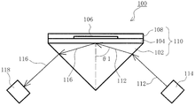
- a metal thin film 104 is formed on the upper surface of a dielectric member 102, and a ligand-containing layer 108 having a ligand fixing region 106 is arranged on the metal thin film 104.
- a sensor structure 110 is provided.
- the dielectric member 102 side of the sensor structure 110 includes a light source 114 that irradiates the excitation light 112 toward the metal thin film 104, and receives reflected light 116 that is irradiated from the light source 114 and reflected by the metal thin film 104.
- a light receiving means 118 is provided.
- a ligand is fixed to the ligand fixing region 106 on the metal thin film 104, and a sample solution containing a specific analyte is supplied thereto.
- the excitation light 112 is irradiated from below the dielectric member 102 toward the metal thin film 104 at the resonance angle ⁇ 1, and the reflected light 116 reflected by the metal thin film 104 is received by the light receiving means 118.
- the resonance angle ⁇ 1 changes depending on the presence or absence of the analyte
- the resonance angle ⁇ 1 at this time is obtained by examining in advance the resonance angle ⁇ 1 when the sample solution not containing the analyte is supplied to the ligand fixing region 106. It can be determined that the predetermined analyte is included.
- SPFS surface plasmon excitation enhanced fluorescence spectroscopy
- SPR surface plasmon resonance
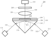
- a metal thin film 204 is first formed on the upper surface of a dielectric member 202, and a ligand-containing layer 208 having a ligand fixing region 206 on the metal thin film 204.
- a sensor structure 210 is provided.
- a light source 214 that irradiates the excitation light 212 toward the metal thin film 204, and a light receiving unit that receives the reflected light 216 irradiated from the light source 214 and reflected by the metal thin film 204. 218 is provided.
- a light detection means 222 that receives the fluorescence 220 emitted from the fluorescent substance labeled with the analyte captured in the ligand fixing region 206 is provided.
- the light collecting member 224 for efficiently collecting the fluorescence 220 and the light contained in the area other than the fluorescence 220 are removed, and only the necessary fluorescence 220 is selected.
- a wavelength selection function member 226 is provided.
- a ligand is fixed to the ligand fixing region 206 on the metal thin film 204, and an analyte labeled with a fluorescent substance is captured on the ligand.
- the light source 214 irradiates the dielectric member 202 with the excitation light 212, and the excitation light 212 is incident on the metal thin film 204 at the resonance angle ⁇ 2, thereby causing a dense wave (surface plasmon) on the metal thin film 204.
- the excitation light 212 and electronic vibration in the metal thin film 204 are coupled to reduce the amount of reflected light 216. If a point where the signal of the received reflected light 216 changes (the amount of light decreases) is found, the resonance angle ⁇ 2 at which the rough wave (surface plasmon) occurs can be obtained.
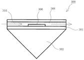
- the ligand fixing region 306 on the metal thin film 304 is disposed in the middle of the horizontal channel 308, and after fixing the ligand to the ligand fixing region 306 in the horizontal channel 308, By feeding a sample solution 310 containing a specific substance (analyte) into the horizontal channel 308, the analyte is captured in the ligand fixing region 306.
- Reference numeral 302 in the figure denotes a dielectric member.
- the sample solution 310 is circulated using a one-way liquid pump or reciprocated using a reciprocating liquid pump. It is devised so that the reaction of the specific substance occurs in any part of the fixed region 306.
- a method of storing the sample solution is also known.
- a well member 408 having a plurality of through holes 410 is disposed on a ligand fixing region 406 on a metal thin film 404 as shown in FIG.
- the analyte is captured in the ligand fixing region 406 in the through hole 410.
- This method has an advantage that the structure can be simplified as compared with the case of using a flow path because it is not necessary to prepare a liquid feed pump unlike the method of performing liquid transfer using a flow path.
- the structure can be simplified as in the SPR apparatus, and the manufacturing cost can be reduced. It is thought that you can.
- the flow of the sample solution is unlikely to occur in the through hole of the well member, and when the specific substance to be detected is extremely small, the specific substance is surely a ligand in the ligand fixing region. May not be captured.
- the present invention can detect a specific substance with high accuracy even when a sensor structure including a well member is used, and is manufactured by simplifying the structure compared to a liquid feeding method using a flow path. It is an object of the present invention to provide a surface plasmon excitation enhanced fluorescence measuring apparatus capable of reducing costs and a fluorescence detection method using the same.
- the surface plasmon excitation enhanced fluorescence measuring device of the present invention is A sensor member comprising: a dielectric member; a metal thin film formed on the dielectric member; and a ligand fixing region formed on the metal thin film; and the ligand fixing region fixed on the sensor member; A well member having a through hole at a corresponding position, and a sensor structure, A light source for irradiating excitation light toward the metal thin film of the sensor structure, and the ligand fixing region on the metal thin film by irradiating the metal thin film with the excitation light from the light source to enhance the electric field on the metal thin film An apparatus main body having at least light detection means for exciting the fluorescent material held in the light source and detecting the fluorescence excited thereby, With The sensor structure is a surface plasmon excitation enhanced fluorescence measurement device configured to be used by being attached to and detached from the device body, or fixed to the device body, The irradiation position of
- the specific substance can be detected with high accuracy by changing the irradiation position of the excitation light.
- the sensor structure including the well member does not require a liquid feeding means such as a flow path or a pump, the manufacturing cost for the apparatus can be suppressed.
- the fluorescence detection method of the present invention comprises: A sensor member comprising a dielectric member, a metal thin film formed on the dielectric member, and a ligand fixing region formed on the metal thin film, and fixed on the sensor member, the ligand fixing region And a well member having a through hole at a corresponding position, and a step of causing the ligand fixed to the ligand fixing region of the sensor structure to capture the analyte, and further labeling the analyte with a fluorescent substance, Irradiating excitation light from the dielectric member side to the metal thin film of the sensor structure in a state where the analyte is labeled with a fluorescent material, and exciting the fluorescent material; Measuring the excited fluorescence with a light detection means; A fluorescence detection method having at least In the step of exciting the fluorescent material, The excitation light is irradiated so that the center of the optical axis of the excitation light is located at a position separated by a predetermined distance from the position of
- the surface plasmon excitation enhanced fluorescence measuring apparatus of the present invention is The irradiation position of the excitation light is When the shortest distance from the center of gravity of the bottom surface region defined by the through hole of the well member to the outer edge of the through hole is 100%, the position is separated from the center of gravity by 1 to 75%. It is characterized by.
- the fluorescence detection method of the present invention comprises: In the step of exciting the fluorescent material,
- the irradiation position of the excitation light is When the shortest distance from the position of the center of gravity of the bottom surface area defined by the through hole of the well member to the outer edge of the through hole is 100%, the position is separated from the position of the center of gravity by 1 to 75%. It is characterized by. If the excitation light irradiation position is defined in such a range, the specific substance can be detected with high accuracy.
- the surface plasmon excitation enhanced fluorescence measuring apparatus of the present invention is The sensor structure is used after being stirred.
- the fluorescence detection method of the present invention comprises: In the step of labeling the analyte with a fluorescent substance, The sensor structure is agitated.
- the analyte can be surely captured by the ligand in the ligand fixing region when the sample solution is supplied into the through hole. Therefore, the specific substance can be detected with high accuracy.
- the surface plasmon excitation enhanced fluorescence measuring apparatus of the present invention is
- the through hole of the well member is provided with a reverse taper that gradually decreases in diameter toward the bottom of the through hole. If the through hole is configured in this way, it is possible to reliably collect the fluorescence generated in a radial manner during fluorescence detection. Therefore, the specific substance can be detected with high accuracy.
- the surface plasmon excitation enhanced fluorescence measuring apparatus of the present invention is The shape of the through hole of the well member is a point-symmetric shape.
- the sample solution when the sample solution is stored in the through hole, the sample solution can easily flow in the through hole, and the analyte can be reliably captured by the ligand in the ligand fixing region. Therefore, the specific substance can be detected with high accuracy.
- the surface plasmon excitation enhanced fluorescence measuring apparatus of the present invention is One ligand is fixed to the ligand fixing region. With this configuration, one type of analyte can be detected.
- the surface plasmon excitation enhanced fluorescence measuring apparatus of the present invention is A plurality of types of ligands are fixed to the ligand fixing region. If comprised in this way, the test
- the surface plasmon excitation enhanced fluorescence measuring apparatus of the present invention is One well hole is provided in the well member. Thus, if there is one through-hole, processing is easy and high positioning accuracy of the ligand fixing region is not required, so that the sensor structure can be easily manufactured.
- the surface plasmon excitation enhanced fluorescence measuring apparatus of the present invention is The well member is provided with a plurality of the through holes. Thus, if there are a plurality of through holes, inspection under the same conditions, multi-item inspection, and further reference can be performed with one sensor structure.
- the surface plasmon excitation enhanced fluorescence measuring apparatus of the present invention is Position adjustment means for adjusting the sensor structure and the light source by moving relative to each other is provided.
- the surface plasmon excitation enhanced fluorescence measuring apparatus of the present invention is The inner wall surface of the through hole of the well member is subjected to a surface treatment for preventing non-specific adsorption.
- a specific substance can be detected with high accuracy, and since the structure is simple, surface plasmon excitation enhanced fluorescence that can reduce manufacturing costs can be achieved.
- a measuring apparatus and a fluorescence detection method using the same can be provided.
- FIG. 1 is a schematic diagram of the SPFS apparatus of the present invention.
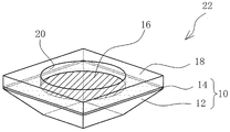
- FIG. 2 is a perspective view of a sensor structure used in the SPFS device of the present invention.
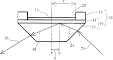
- FIG. 3 is a schematic diagram for explaining the irradiation position of the excitation light in the sensor structure used in the SPFS apparatus of the present invention.
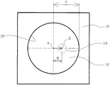
- FIG. 4 is a top view for explaining the irradiation position of the excitation light in the sensor structure used in the SPFS device of the present invention.
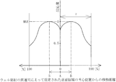
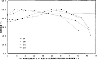
- FIG. 5 is a graph showing the reaction amount distribution of the ligand-containing layer located in the through hole of the well member in the sensor structure used in the SPFS apparatus of the present invention.
- FIG. 6 is a schematic view for explaining the reverse taper attached to the through hole of the well member in the sensor structure used in the SPFS device of the present invention.
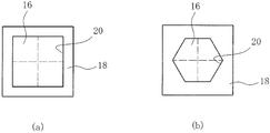
- FIG. 7 is a top view for explaining the shape of the through hole of the well member in the sensor structure used in the SPFS device of the present invention.
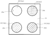
- FIG. 8 is a top view for explaining a state in which a plurality of types of ligands are fixed to a ligand fixing region located in one through hole in the sensor structure used in the SPFS device of the present invention.
- FIG. 9 is a top view for explaining a state in which different types of ligands are fixed to the ligand fixing regions located in the through holes in the plurality of through holes in the sensor structure used in the SPFS device of the present invention. It is.
- FIG. 8 is a schematic view for explaining the reverse taper attached to the through hole of the well member in the sensor structure used in the SPFS device of the present invention.
- FIG. 7 is a top view for explaining the shape of the through hole
- FIG. 10 is a schematic view of a sensor structure in another embodiment used in the SPFS apparatus of the present invention.
- FIG. 11 is a graph showing the reaction amount distribution of the ligand-containing layer located in the through hole of the well member in the sensor structures of Examples 1 to 3.
- FIG. 12 is a schematic diagram of a conventional SPR device.
- FIG. 13 is a schematic diagram of a conventional SPFS apparatus.
- FIG. 14 is a schematic diagram for explaining a supply method using a channel as a method of supplying a sample solution to a ligand fixing region in a conventional sensor structure.
- FIG. 15 is a schematic diagram for explaining a supply method using a well member as a method for supplying a sample solution to a ligand fixing region in a conventional sensor structure.
- the surface plasmon excitation enhanced fluorescence measuring device (SPFS device) of the present invention is a device that performs fluorescence detection with high sensitivity by surely exciting a fluorescent substance labeled with an analyte captured by a ligand fixed in a ligand fixing region. It is.
- the “surface plasmon” in the present specification is used in a broad sense, and includes “localized plasmon”. Further, the “bottom area defined by the through hole of the well member” is an area defined by the opening end of the through hole on the metal thin film side.
- the SPFS device 1 of the present invention includes a dielectric member 12, a metal thin film 14 formed on the upper surface of the dielectric member 12, and an analyte to be detected on the upper surface of the metal thin film 14.
- a well having a sensor member 10 having a ligand fixing region 16 for fixing a ligand that specifically adsorbs, and having a through hole 20 on the sensor member 10 at a position corresponding to the ligand fixing region 16.
- a sensor structure 22 to which the member 18 is fixed is provided.
- a ligand is fixed on the entire surface of the metal thin film 14, and in this state, a well member 18 is formed on the metal thin film 14.
- the ligand is already immobilized on the ligand fixing region 16 on the metal thin film 14 before the well member 18 is fixed, the ligand is not attached to the inner wall surface of the through hole 20 of the well member 18 and the detection efficiency is increased. It is preferable for increasing the ratio.
- the ligand is immobilized on the entire surface of the metal thin film 14, it is not necessary to use a separate member for restricting the ligand to the ligand-fixed region 16 when the ligand is immobilized.
- the ligand fixing region 16 is included in the same region or includes the ligand fixing region 16, and is fixed to a slightly wider region. You can also. In this case, it is preferable to immobilize the ligand on the metal thin film 14 using a frame member different from the well member 18.
- the ligand may be immobilized only on the metal thin film 14 located on the bottom surface of the through hole 20 by arranging 18 and injecting a solution containing the ligand into the through hole 20.
- a well-known processing method can be used, for example, the solution containing proteins, such as BSA and casein, and a phospholipid analog synthetic polymer (NOF Corporation) By using the contained solution, nonspecific adsorption can be effectively prevented.
- the solution containing proteins such as BSA and casein
- a phospholipid analog synthetic polymer NOF Corporation
- the dielectric member 12 is a hexahedron having a substantially trapezoidal cross section (a truncated quadrangular pyramid shape), and the well member 18 has a square shape corresponding to the shape of the dielectric member 12. It is configured.
- the shape of the dielectric member 12 is not limited to the form shown in FIG. 2, and may be, for example, a pyramid shape such as a quadrangular pyramid, a cone, a triangular pyramid, a polygonal pyramid, or a truncated pyramid shape. Is.
- the sensor structure 22 includes a light source 26 that is incident on the dielectric member 12 and irradiates the excitation light 24 toward the metal thin film 14 on the dielectric member 12 side.
- a light receiving means 30 is provided for receiving the reflected light 28 reflected by the light.
- the excitation light 24 emitted from the light source 26 is preferably laser light, and an LD laser having a wavelength of 200 to 900 nm and 0.001 to 1,000 mW, or a semiconductor laser having a wavelength of 230 to 800 nm and 0.01 to 100 mW is suitable. .
- light detection means 34 for receiving the fluorescence 32 generated in the ligand fixing region 16 is provided.
- the light detection means 34 it is preferable to use an ultrasensitive photomultiplier tube or a CCD image sensor capable of multipoint measurement.
- a light collecting member 36 for efficiently collecting light and a fluorescent light 32 only in the light are selected.
- the wavelength selection function member 38 is provided, and this constitutes the apparatus main body.
- the SPFS apparatus 1 shown in FIG. 1 intends the form that the sensor structure 22 is attached to and detached from the apparatus main body, it is not limited to such a form.
- the sensor structure 22 may be configured to be used while being fixed to the apparatus main body.
- any condensing system can be used as long as it condenses the fluorescent signal efficiently.
- a simple condensing system a commercially available objective lens used in a microscope or the like can be used.
- the magnification of the objective lens is preferably 10 to 100 times.
- an optical filter As the wavelength selection function member 38, an optical filter, a cut filter, or the like can be used.
- the optical filter include a neutral density (ND) filter and a diaphragm lens.
- the cut filter includes external light (illumination light outside the device), excitation light (excitation light transmission component), stray light (excitation light scattering component in various places), and plasmon scattering light (excitation light originated from the sensor)
- a ligand that specifically adsorbs to the analyte to be detected in the ligand fixing region 16 on the metal thin film 14 of the sensor structure 22 is supplied into the through hole 20 in a state where the sensor structure 22 is fixed, and the sensor structure 22 is agitated.
- the ligand fixing region 16 it is preferable to fix the ligand to the ligand fixing region 16 before the fluorescence detection in advance in order to reduce the time required for the fluorescence detection. You can go right before.
- the light source 26 irradiates the metal thin film 14 with the excitation light 24, and the excitation light 24 is at a specific angle (resonance angle (angle formed by the excitation light 24 and the perpendicular of the metal thin film 14 when the electric field is enhanced) ⁇ a).
- a specific angle resonance angle (angle formed by the excitation light 24 and the perpendicular of the metal thin film 14 when the electric field is enhanced) ⁇ a.
- the fluorescent material generated in the ligand fixing region 16 on the metal thin film 14 is efficiently excited, thereby increasing the amount of fluorescence 32 emitted from the fluorescent material, and collecting this fluorescence 32.
- the light detection means 34 By receiving light by the light detection means 34 through the optical member 36 and the wavelength selection function member 38, it is possible to detect an extremely small amount and / or extremely low concentration of the analyte.
- the material of the metal thin film 14 of the sensor structure 22 is preferably made of at least one metal selected from the group consisting of gold, silver, aluminum, copper, and platinum, more preferably made of gold. It consists of a metal alloy. Such a metal is suitable for the metal thin film 14 because it is stable against oxidation and the electric field enhancement due to the dense wave (surface plasmon) becomes large.
- examples of the method for forming the metal thin film 14 include sputtering, vapor deposition (resistance heating vapor deposition, electron beam vapor deposition, etc.), electrolytic plating, electroless plating, and the like.
- the sputtering method and the vapor deposition method are preferable because the thin film formation conditions can be easily adjusted.
- the thickness of the metal thin film 14 ranges from gold: 5 to 500 nm, silver: 5 to 500 nm, aluminum: 5 to 500 nm, copper: 5 to 500 nm, platinum: 5 to 500 nm, and alloys thereof: 5 to 500 nm. It is preferable to be within. From the viewpoint of the electric field enhancement effect, within the range of gold: 20-70 nm, silver: 20-70 nm, aluminum: 10-50 nm, copper: 20-70 nm, platinum: 20-70 nm, and alloys thereof: 10-70 nm More preferably.
- the thickness of the metal thin film 14 is within the above range, close-packed waves (surface plasmons) are easily generated, which is preferable. Moreover, if it is the metal thin film 14 which has such thickness, a magnitude
- specimens used at the time of analyte detection include blood, serum, plasma, urine, nasal fluid, saliva, feces, body cavity fluid (eg, cerebrospinal fluid, ascites, pleural effusion).
- the analyte contained in the sample is, for example, a nucleic acid (DNA, RNA, polynucleotide, oligonucleotide, PNA (peptide nucleic acid), which may be single-stranded or double-stranded, or nucleoside.
- Nucleotides and their modified molecules Nucleotides and their modified molecules), proteins (polypeptides, oligopeptides, etc.), amino acids (including modified amino acids), carbohydrates (oligosaccharides, polysaccharides, sugar chains, etc.), lipids, or modified molecules thereof, Specific examples thereof include a complex, and may be a carcinoembryonic antigen such as AFP ( ⁇ -fetoprotein), a tumor marker, a signal transduction substance, a hormone, and the like, and is not particularly limited.
- AFP ⁇ -fetoprotein
- the fluorescent substance is not particularly limited as long as it is a substance that emits fluorescence 32 by being irradiated with predetermined excitation light 24 or excited by using a field effect.
- the fluorescence 32 as used in this specification includes various light emission, such as phosphorescence.
- the dielectric member 12 various optically transparent inorganic substances, natural polymers, and synthetic polymers can be used. From the viewpoints of chemical stability, manufacturing stability, and optical transparency, silicon dioxide (SiO 2). 2 ) or titanium dioxide (TiO 2 ).
- the well member 18 various materials such as synthetic resin, metal, and ceramics can be used.
- the through hole 20 can be provided by machining.
- an adhesive, matching oil, a transparent adhesive sheet or the like having the same optical refractive index as that of the dielectric member 12.
- the size of the through hole 20 of the well member 18 is preferably set to have a capacity of, for example, 80 to 100 ⁇ l.
- such an SPFS device 1 adjusts the optimum angle (resonance angle ⁇ a) of surface plasmon resonance by the excitation light 24 irradiated from the light source 26 to the metal thin film 14,
- a computer (not shown) for processing information input to the light detection means 34 may be included.
- the angle variable unit (not shown) synchronizes the light receiving means 30 and the light source 26 in order to obtain the total reflection attenuation (ATR) condition by a servo motor, and allows an angle change of 45 to 85 °, and the resolution. Is preferably 0.01 ° or more.
- the excitation light irradiated from the light source 26 to the metal thin film 14.
- the excitation light 24 is arranged such that the optical axis center of the excitation light 24 is positioned at a position separated from the gravity center position A of the bottom surface region defined by the through hole 20 of the well member 18 by a predetermined distance H.
- the irradiation position is set.
- the symbol r is the shortest distance from the center of gravity position A of the bottom surface region of the through hole 20 to the outer edge of the through hole 20.
- the irradiation position of the excitation light 24 when the irradiation position of the excitation light 24 is moved, it is preferable to move the light source 26 using the position adjusting means 40 described above.
- the sensor structure 22 itself may be moved.
- the light source 26 and the sensor structure 22 are not particularly limited as long as they can be moved relative to each other.
- the sample solution containing the sample is supplied into the through hole 20 of the well member 18 so that the sample (analyte) is reliably captured by the ligand fixed in the ligand fixing region 16. After that, the sensor structure 22 is stirred.
- the stirring method here is preferably stirring by circular motion, and can be performed using, for example, a dedicated stirring device (not shown).
- a dedicated stirring device not shown.
- the sample solution is moved in a circle in the through hole 20 of the well member 18.
- how the reaction amount of the ligand and the analyte in the ligand fixing region 16 is distributed is examined by staining the ligand fixing region 16 after stirring with gold colloid. Starting from the center of gravity position A of the defined bottom area, it was confirmed that portions with a high reaction amount were distributed in a donut shape.
- the reaction amount value is highest at a position B moved by a predetermined distance from the gravity center position A of the bottom surface region defined by the through hole 20 of the well member 18 as shown in FIG. I understand that
- the present inventor has found that the detection efficiency of the fluorescence 32 can be effectively increased by setting the irradiation position B of the excitation light 24 according to the position where the value of the reaction amount is the highest.
- the distribution of the reaction amount is different if the measurement conditions such as the size of the through hole 20 and the type of the ligand are different. It was found that when the shortest distance r is set to 100%, the value of the reaction amount generally increases when the position is in the range of 1 to 75% from the center of gravity position A.
- the movement range of the irradiation position of the excitation light 24 is within a range in which the diameter of the optical axis of the excitation light 24 is within the through hole 20.
- the distribution of the reaction amount after stirring of the sensor structure 22 is examined, and the irradiation position of the excitation light 24 is set at the position where the value of the reaction amount is the highest.
- the detection efficiency of the fluorescence 32 can be effectively increased.
- the sensor structure 22 used in the SPFS apparatus 1 of the present invention uses the well member 18, a liquid feeding means such as a pump like the flow path type sensor structure 300 as shown in FIG.
- the manufacturing cost can be reduced by simplifying the apparatus.
- the through hole 20 of the well member 18 is straight.
- the reverse taper gradually decreases in diameter toward the bottom of the through hole 20. 44 may be attached.
- the reason is that the fluorescence 32 generated from the fluorescent material is diffused radially, and the diffused fluorescence 32 is efficiently collected by the light detection means 34.
- the inclination angle ⁇ b of the inverse taper 44 is preferably in the range of more than 0 ° and 45 ° or less in order to increase the light collection efficiency.
- the shape of the through hole 20 is not limited to a circle as in the present embodiment, and may be an ellipse or a triangle, but the quadrangle shown in FIG. A point-symmetric shape such as the hexagon shown in FIG. 7 (b) is preferable because a reaction distribution appears remarkably when stirring is performed.
- the irradiation position of the excitation light 24 is set with the shortest distance r from the gravity center position A of the bottom surface region of the through hole 20 to the outer edge of the through hole 20 being 100%. It should be specified.
- a plurality of types of ligands 16 a to 16 d fixed to the ligand fixing region 16 may be provided for one through hole 20.
- a well member 18 having a plurality of through holes 20 may be used. In this case, different ligands 16e to 16h may be fixed to each through hole 20. It is.
- the sensor structure 22 rotates relative to the light source 26. If such a moving means (not shown) is provided separately, fluorescence detection can be performed smoothly.
- the well member 18 is fixed on the metal thin film 14, but as shown in FIG. 10, the metal thin film 14 is partially formed on the sensor structure 22 by a method such as patterning. Further, a structure may be adopted in which a ligand fixing region 16 is formed on the metal thin film 14 and a well member 18 is placed on the dielectric member 12 so as to surround the ligand fixing region 16 and the metal thin film 14. It is.
- the SPFS device 1 and the fluorescence detection method using the SPFS device 1 according to the present invention have been described above.
- the present invention is not limited to the above-described embodiment.
- the configuration of the device main body described in the above-described embodiment is further simplified. It is also possible to make various changes without departing from the object of the present invention.
- Example 1 After the metal thin film 14 was formed on the upper surface of the dielectric member 12, a ligand that specifically adsorbs to the analyte to be detected was fixed on the metal thin film 14 to form the ligand fixing region 16.
- a well member 18 having a circular through hole 20 having a diameter of 5 mm was prepared, and this was fixed on the metal thin film 14 with matching oil to form a sensor structure 22.
- a sample solution containing a specimen was injected into the through-hole 20 of the sensor structure 22, and this was set in a stirring device that was stirred by a circular motion and stirred.
- the specimen (analyte) in the ligand fixing region 16 was stained with colloidal gold, and the staining state was confirmed with a CCD camera. It was confirmed that a reaction distribution was generated in a donut shape starting from the center of gravity A of the bottom region defined by the hole 20.
- the reaction distribution was graphed as shown in FIG.
- the X axis of the graph is from the center of gravity position A of the bottom surface region of the through hole 20 when the shortest distance r from the center of gravity A of the bottom surface region of the through hole 20 of the well member 18 to the outer edge of the through hole 20 is 100%.
- the Y-axis is the reaction amount, and represents the ratio when the maximum value of the reaction amount is 100%.
- Example 2 A sensor structure 22 is manufactured in the same manner as in Example 1 except that the well member 18 having a circular through hole 20 having a diameter of 6.5 mm is used, and the sensor structure 22 is set in a stirring device that stirs in a circular motion. I let you.
- the specimen in the ligand fixing region 16 is stained with colloidal gold, and the staining state is confirmed by a CCD camera. It was confirmed that the reaction distribution occurred in a donut shape starting from the center of gravity position A of the bottom surface area.
- reaction amount shows the maximum value at a position 15% away from the center of gravity position A of the bottom surface region defined by the through hole 20 of the well member 18. confirmed.
- Example 3 A sensor structure 22 was manufactured in the same manner as in Example 1 except that the well member 18 having a circular through hole 20 having a diameter of 12 mm was used, and this was set in a stirring device that was stirred by a circular motion and stirred. .
- the specimen in the ligand fixing region 16 was stained with colloidal gold, and the staining state was confirmed with a CCD camera. It was confirmed that the reaction distribution occurred in a donut shape starting from the center of gravity position A of the bottom surface area.
- reaction amount shows the maximum value at a position spaced 50% from the center of gravity position A of the bottom surface region defined by the through hole 20 of the well member 18. confirmed.
- Example 4 A sensor structure 22 was manufactured in the same manner as in Example 1 except that the well member 18 having a circular through hole 20 having a diameter of ⁇ 18 mm was used, and this was set in a stirring device for stirring by circular motion and stirred. .
- the specimen in the ligand fixing region 16 is stained with colloidal gold, and the staining state is confirmed by a CCD camera. It was confirmed that the reaction distribution occurred in a donut shape starting from the center of gravity position A of the bottom surface area.
- reaction amount shows the maximum value at a position 61% away from the center of gravity position A of the bottom surface region defined by the through hole 20 of the well member 18. confirmed.
- the size of the through hole 20 in Examples 1 to 4 is generally the minimum size to the maximum size of the through hole 20 of the well member 18 that is commercially available. Therefore, from the results of Examples 1 to 4, even if the size of the through hole 20 of the well member 18 is changed, the moving distance from the center of gravity position A of the bottom surface region defined by the through hole 20 of the well member 18 is 1 to 75. It was confirmed that if the irradiation position of the excitation light 24 was set at a position within the range of%, a generally good reaction occurred.
- SPFS device Surface plasmon excitation enhanced fluorescence measuring device
- Sensor member 12 ... Dielectric member 14 ... Metal thin film 16 ; Ligand fixed area
- Well member Center of gravity position of bottom surface area defined by through hole B Irradiation position of excitation light irradiated to metal thin film from light source H: Separation distance (predetermined distance) r: Shortest distance from the center of gravity of the bottom region of the through hole to the outer edge of the through hole 100 ...
- Surface plasmon resonance device (SPR device) DESCRIPTION OF SYMBOLS 102 ...
- Dielectric member 104 ... Metal thin film 106 ... Ligand fixed area
- SPFS device Surface plasmon excitation enhanced fluorescence measuring device
- Dielectric member 204 Dielectric member 204
- Metal thin film 206 ... Ligand fixing region 208 ... Ligand-containing layer 210 ...
- Sensor structure 212 ... Excitation light 214 ... Light source 216 ... Reflection Light 218 ... Light receiving means 220 ... Fluorescence 222 ... Light detecting means 224 ... Condensing member 226 ... Wavelength selection function member 300 ...
Landscapes
- Health & Medical Sciences (AREA)
- Immunology (AREA)
- Chemical & Material Sciences (AREA)
- Physics & Mathematics (AREA)
- Biochemistry (AREA)
- Nuclear Medicine, Radiotherapy & Molecular Imaging (AREA)
- Life Sciences & Earth Sciences (AREA)
- Analytical Chemistry (AREA)
- General Health & Medical Sciences (AREA)
- General Physics & Mathematics (AREA)
- Pathology (AREA)
- Optics & Photonics (AREA)
- Chemical Kinetics & Catalysis (AREA)
- Investigating, Analyzing Materials By Fluorescence Or Luminescence (AREA)
- Optical Measuring Cells (AREA)
Abstract
Description
一方、このような表面プラズモン共鳴(SPR)現象を応用した表面プラズモン励起増強蛍光分光法(SPFS)の原理に基づき、SPR装置100よりもさらに高精度にアナライトの検出を行えるようにした表面プラズモン励起増強蛍光測定装置(以下、SPFS装置ともいう)も開発されている。
ところで、SPR装置100のリガンド固定領域106やSPFS装置200のリガンド固定領域206へ試料溶液を供給する方法としては、例えば流路を用いて送液する供給方法が知られている。
特許文献1に開示されたセンサ構造体400では、図15に示したように金属薄膜404上のリガンド固定領域406の上に、複数の貫通穴410を有するウェル部材408を配設し、各貫通穴410内に試料溶液412を供給して貯留させることで、貫通穴410内のリガンド固定領域406にアナライトが捕捉されるようにしている。
本発明の表面プラズモン励起増強蛍光測定装置は、
誘電体部材と、前記誘電体部材上に形成された金属薄膜と、前記金属薄膜上に形成されたリガンド固定領域と、を備えたセンサ部材と、前記センサ部材上に固定され前記リガンド固定領域と対応する位置に貫通穴を有するウェル部材と、から成るセンサ構造体と、
前記センサ構造体の金属薄膜に向かって励起光を照射する光源と、前記光源より前記金属薄膜に励起光を照射し、前記金属薄膜上の電場を増強させて前記金属薄膜上の前記リガンド固定領域に保持された蛍光物質を励起させ、これにより励起された蛍光を検出する光検出手段と、を少なくとも有する装置本体と、
を備え、
前記センサ構造体が、前記装置本体に対して着脱されて使用される、または前記装置本体に対して固定されて使用されるよう構成された表面プラズモン励起増強蛍光測定装置であって、
前記センサ構造体のウェル部材の貫通穴によって規定された底面領域の重心位置から所定距離離間した位置に、前記励起光の光軸中心が位置するよう前記励起光の照射位置が設定されていることを特徴とする。
誘電体部材と、前記誘電体部材上に形成された金属薄膜と、前記金属薄膜上に形成されたリガンド固定領域と、を備えたセンサ部材と、前記センサ部材上に固定され、前記リガンド固定領域と対応する位置に貫通穴を有するウェル部材と、から成るセンサ構造体の前記リガンド固定領域に固定されたリガンドにアナライトを捕捉させ、さらに前記アナライトを蛍光物質で標識する工程と、
前記アナライトを蛍光物質で標識した状態で、前記センサ構造体の金属薄膜に前記誘電体部材側から励起光を照射して、前記蛍光物質を励起させる工程と、
励起された蛍光を光検出手段にて測定する工程と、
を少なくとも有する蛍光検出方法であって、
前記蛍光物質を励起させる工程において、
前記センサ構造体のウェル部材の貫通穴によって規定された底面領域の重心位置から所定距離離間した位置に、前記励起光の光軸中心が位置するよう前記励起光が照射されることを特徴とする。
このような蛍光検出方法であれば、特定物質を精度良く検出することができる。
前記励起光の照射位置が、
前記ウェル部材の貫通穴によって規定された底面領域の重心位置から前記貫通穴の外形端までの最短距離を100%とした場合、前記重心位置から1~75%の範囲で離間した位置であることを特徴とする。
前記蛍光物質を励起させる工程において、
前記励起光の照射位置が、
前記ウェル部材の貫通穴によって規定された底面領域の重心位置から前記貫通穴の外形端までの最短距離を100%とした場合、前記重心位置から1~75%の範囲で離間した位置であることを特徴とする。
このような範囲に励起光の照射位置を規定すれば、精度良く特定物質を検出することができる。
前記センサ構造体は、撹拌されて使用されることを特徴とする。
前記アナライトを蛍光物質で標識する工程において、
前記センサ構造体は、撹拌されることを特徴とする。
前記ウェル部材の前記貫通穴には、前記貫通穴の底に向かって次第に径が小さくなる逆テーパーが付されていることを特徴とする。
このように貫通穴が構成されていれば、蛍光検出の際に放射状に生ずる蛍光を確実に集光することができる。したがって、精度良く特定物質を検出することができる。
前記ウェル部材の前記貫通穴の形状が、点対称な形状であることを特徴とする。
前記リガンド固定領域に固定されるリガンドが1種類であることを特徴とする。
このように構成すれば、1種類のアナライトを検出することができる。
前記リガンド固定領域に固定されるリガンドが複数種類であることを特徴とする。
このように構成すれば、同一条件での検査や多項目検査、さらにはリファレンスなどを1つのセンサ構造体で行うことができる。
前記ウェル部材には、前記貫通穴が1つ設けられていることを特徴とする。
このように貫通穴が1つであれば、加工が容易であり、リガンド固定領域の高い位置決め精度も要求されないのでセンサ構造体の製造を容易に行うことができる。
前記ウェル部材には、前記貫通穴が複数設けられていることを特徴とする。
このように貫通穴が複数で有れば、同一条件での検査や多項目検査、さらにはリファレンスなどを1つのセンサ構造体で行うことができる。
前記センサ構造体と前記光源とを、相対的に移動させて調整する位置調整手段を有することを特徴とする。
前記ウェル部材の前記貫通穴の内壁面に、非特異吸着防止用の表面処理が施されていることを特徴とする。
本発明の表面プラズモン励起増強蛍光測定装置(SPFS装置)は、リガンド固定領域に固定されたリガンドに捕捉されたアナライトを標識した蛍光物質を、確実に励起させて高感度に蛍光検出を行うものである。
さらに「ウェル部材の貫通穴によって規定された底面領域」とは、貫通穴の金属薄膜側の開口端で区画された領域のことである。
また別の製造方法として、誘電体部材12の上面に金属薄膜14を成膜した後、金属薄膜14上に、予め貫通穴20の内壁面に非特異吸着防止用の表面処理を施したウェル部材18を配設し、貫通穴20内にリガンドを含有した溶液を注入することで、貫通穴20の底面に位置する金属薄膜14の上にのみリガンドを固定化させるようにしても良い。
そして、センサ構造体22の誘電体部材12側には、誘電体部材12内に入射され、金属薄膜14に向かって励起光24を照射する光源26を備え、さらに光源26から照射され金属薄膜14に反射した反射光28を受光する受光手段30が備えられている。
光源26から照射される励起光24としてはレーザ光が好ましく、波長200~900nm、0.001~1,000mWのLDレーザ、または波長230~800nm、0.01~100mWの半導体レーザが好適である。
光検出手段34としては、超高感度の光電子増倍管、または多点計測が可能なCCDイメージセンサを用いることが好ましい。
光学フィルタとしては、減光(ND)フィルタ,ダイアフラムレンズなどが挙げられる。
また、検体中に含有されるアナライトは、例えば、核酸(一本鎖であっても二本鎖であってもよいDNA,RNA,ポリヌクレオチド,オリゴヌクレオチド,PNA(ペプチド核酸)等、またはヌクレオシド,ヌクレオチドおよびそれらの修飾分子),タンパク質(ポリペプチド、オリゴペプチド等),アミノ酸(修飾アミノ酸も含む。),糖質(オリゴ糖,多糖類,糖鎖等),脂質,またはこれらの修飾分子,複合体などが挙げられ、具体的には、AFP(αフェトプロテイン)等のがん胎児性抗原や腫瘍マーカー,シグナル伝達物質,ホルモンなどであってもよく、特に限定されない。
また、センサ部材10上にウェル部材18を固定する際には、誘電体部材12と同じ光屈折率を有する接着剤,マッチングオイル,透明粘着シートなどを用いることが好ましい。
また、このようなSPFS装置1は、光源26から金属薄膜14に照射される励起光24による表面プラズモン共鳴の最適角(共鳴角θa)を調整するため、角度可変部(図示せず)や、光検出手段34に入力された情報を処理するためのコンピュータ(図示せず)などを有しても良いものである。
なおセンサ構造体22を円運動で撹拌すると、ウェル部材18の貫通穴20内で試料溶液が円を描くように移動される。この時、リガンド固定領域16におけるリガンドとアナライトとの反応量がどのように分布するか、撹拌後のリガンド固定領域16に金コロイドで染色して調べたところ、ウェル部材18の貫通穴20によって規定された底面領域の重心位置Aを起点にして、ドーナッツ状に反応量の高い箇所が分布していることが確認された。
逆テーパー44の傾斜角度θbとしては、集光効率を高める上で0°より大きく45°以下の範囲内であることが好ましい。
また、図9に示したように、複数の貫通穴20を有するウェル部材18を用いても良く、この場合には貫通穴20毎に異なるリガンド16e~16hを固定化するようにしても良いものである。
誘電体部材12の上面に金属薄膜14を成膜した後、金属薄膜14上に検出対象となるアナライトと特異的に吸着するリガンドを固定してリガンド固定領域16を形成した。
次いでセンサ構造体22の貫通穴20内に検体(アナライト)を含有した試料溶液を注入し、これを円運動で撹拌する撹拌装置にセットして撹拌させた。
直径φ6.5mmの円形の貫通穴20を有するウェル部材18を用いたこと以外は実施例1と同様にしてセンサ構造体22を製造し、これを円運動で撹拌する撹拌装置にセットして撹拌させた。
直径φ12mmの円形の貫通穴20を有するウェル部材18を用いたこと以外は実施例1と同様にしてセンサ構造体22を製造し、これを円運動で撹拌する撹拌装置にセットして撹拌させた。
直径φ18mmの円形の貫通穴20を有するウェル部材18を用いたこと以外は実施例1と同様にしてセンサ構造体22を製造し、これを円運動で撹拌する撹拌装置にセットして撹拌させた。
10・・・センサ部材
12・・・誘電体部材
14・・・金属薄膜
16・・・リガンド固定領域
16a~16h・・リガンド
18・・・ウェル部材
20・・・貫通穴
20a~20d・・貫通穴
22・・・センサ構造体
24・・・励起光
26・・・光源
28・・・反射光
30・・・受光手段
32・・・蛍光
34・・・光検出手段
36・・・集光部材
38・・・波長選択機能部材
40・・・位置調整手段
42・・・位置調整手段
44・・・逆テーパー
θa・・・共鳴角
θb・・・逆テーパーの傾斜角度
A・・・ウェル部材の貫通穴によって規定された底面領域の重心位置
B・・・光源から金属薄膜に照射される励起光の照射位置
H・・・離間距離(所定距離)
r・・・貫通穴の底面領域の重心位置から貫通穴の外形端までの最短距離
100・・・表面プラズモン共鳴装置(SPR装置)
102・・・誘電体部材
104・・・金属薄膜
106・・・リガンド固定領域
108・・・リガンド含有層
110・・・センサ構造体
112・・・励起光
114・・・光源
116・・・反射光
118・・・受光手段
θ1・・・共鳴角
θ2・・・共鳴角
200・・・表面プラズモン励起増強蛍光測定装置(SPFS装置)
202・・・誘電体部材
204・・・金属薄膜
206・・・リガンド固定領域
208・・・リガンド含有層
210・・・センサ構造体
212・・・励起光
214・・・光源
216・・・反射光
218・・・受光手段
220・・・蛍光
222・・・光検出手段
224・・・集光部材
226・・・波長選択機能部材
300・・・センサ構造体
302・・・誘電体部材
304・・・金属薄膜
306・・・リガンド固定領域
308・・・横形流路
310・・・試料溶液
400・・・センサ構造体
402・・・誘電体部材
404・・・金属薄膜
406・・・リガンド固定領域
408・・・ウェル部材
410・・・貫通穴
412・・・試料溶液
Claims (14)
- 誘電体部材と、前記誘電体部材上に形成された金属薄膜と、前記金属薄膜上に形成されたリガンド固定領域と、を備えたセンサ部材と、前記センサ部材上に固定され前記リガンド固定領域と対応する位置に貫通穴を有するウェル部材と、から成るセンサ構造体と、
前記センサ構造体の金属薄膜に向かって励起光を照射する光源と、前記光源より前記金属薄膜に励起光を照射し、前記金属薄膜上の電場を増強させて前記金属薄膜上の前記リガンド固定領域に保持された蛍光物質を励起させ、これにより励起された蛍光を検出する光検出手段と、を少なくとも有する装置本体と、
を備え、
前記センサ構造体が、前記装置本体に対して着脱されて使用される、または前記装置本体に対して固定されて使用されるよう構成された表面プラズモン励起増強蛍光測定装置であって、
前記センサ構造体のウェル部材の貫通穴によって規定された底面領域の重心位置から所定距離離間した位置に、前記励起光の光軸中心が位置するよう前記励起光の照射位置が設定されていることを特徴とする表面プラズモン励起増強蛍光測定装置。 - 前記励起光の照射位置が、
前記ウェル部材の貫通穴によって規定された底面領域の重心位置から前記貫通穴の外形端までの最短距離を100%とした場合、前記重心位置から1~75%の範囲で離間した位置であることを特徴とする請求項1に記載の表面プラズモン励起増強蛍光測定装置。 - 前記センサ構造体は、撹拌されて使用されることを特徴とする請求項1または2に記載の表面プラズモン励起増強蛍光測定装置。
- 前記ウェル部材の前記貫通穴には、前記貫通穴の底に向かって次第に径が小さくなる逆テーパーが付されていることを特徴とする請求項1~3のいずれかに記載の表面プラズモン励起増強蛍光測定装置。
- 前記ウェル部材の前記貫通穴の形状が、点対称な形状であることを特徴とする請求項1~4のいずれかに記載の表面プラズモン励起増強蛍光測定装置。
- 前記リガンド固定領域に固定されるリガンドが1種類であることを特徴とする請求項1~5のいずれかに記載の表面プラズモン励起増強蛍光測定装置。
- 前記リガンド固定領域に固定されるリガンドが複数種類であることを特徴とする請求項1~5のいずれかに記載の表面プラズモン励起増強蛍光測定装置。
- 前記ウェル部材には、前記貫通穴が1つ設けられていることを特徴とする請求項1~7のいずれかに記載の表面プラズモン励起増強蛍光測定装置。
- 前記ウェル部材には、前記貫通穴が複数設けられていることを特徴とする請求項1~7のいずれかに記載の表面プラズモン励起増強蛍光測定装置。
- 前記センサ構造体と前記光源とを、相対的に移動させて調整する位置調整手段を有することを特徴とする請求項1~9のいずれかに記載の表面プラズモン励起増強蛍光測定装置。
- 前記ウェル部材の前記貫通穴の内壁面に、非特異吸着防止用の表面処理が施されていることを特徴とする請求項1~10のいずれかに記載の表面プラズモン励起増強蛍光測定装置。
- 誘電体部材と、前記誘電体部材上に形成された金属薄膜と、前記金属薄膜上に形成されたリガンド固定領域と、を備えたセンサ部材と、前記センサ部材上に固定され、前記リガンド固定領域と対応する位置に貫通穴を有するウェル部材と、から成るセンサ構造体の前記リガンド固定領域に固定されたリガンドにアナライトを捕捉させ、さらに前記アナライトを蛍光物質で標識する工程と、
前記アナライトを蛍光物質で標識した状態で、前記センサ構造体の金属薄膜に前記誘電体部材側から励起光を照射して、前記蛍光物質を励起させる工程と、
励起された蛍光を光検出手段にて測定する工程と、
を少なくとも有する蛍光検出方法であって、
前記蛍光物質を励起させる工程において、
前記センサ構造体のウェル部材の貫通穴によって規定された底面領域の重心位置から所定距離離間した位置に、前記励起光の光軸中心が位置するよう前記励起光が照射されることを特徴とする蛍光検出方法。 - 前記蛍光物質を励起させる工程において、
前記励起光の照射位置が、
前記ウェル部材の貫通穴によって規定された底面領域の重心位置から前記貫通穴の外形端までの最短距離を100%とした場合、前記重心位置から1~75%の範囲で離間した位置であることを特徴とする請求項12に記載の蛍光検出方法。 - 前記アナライトを蛍光物質で標識する工程において、
前記センサ構造体は、撹拌されることを特徴とする請求項12または13に記載の蛍光検出方法。
Priority Applications (3)
| Application Number | Priority Date | Filing Date | Title |
|---|---|---|---|
| EP12785616.9A EP2711689B1 (en) | 2011-05-19 | 2012-04-23 | Surface plasmon-field enhanced fluorescence measurement device and fluorescence detection method using same |
| US14/118,341 US9551662B2 (en) | 2011-05-19 | 2012-04-23 | Surface plasmon-field enhanced fluorescence measurement device and fluorescence detection method using the same |
| JP2013515054A JP5971240B2 (ja) | 2011-05-19 | 2012-04-23 | 表面プラズモン励起増強蛍光測定装置およびこれを用いた蛍光検出方法 |
Applications Claiming Priority (2)
| Application Number | Priority Date | Filing Date | Title |
|---|---|---|---|
| JP2011-112365 | 2011-05-19 | ||
| JP2011112365 | 2011-05-19 |
Publications (1)
| Publication Number | Publication Date |
|---|---|
| WO2012157403A1 true WO2012157403A1 (ja) | 2012-11-22 |
Family
ID=47176739
Family Applications (1)
| Application Number | Title | Priority Date | Filing Date |
|---|---|---|---|
| PCT/JP2012/060814 Ceased WO2012157403A1 (ja) | 2011-05-19 | 2012-04-23 | 表面プラズモン励起増強蛍光測定装置およびこれを用いた蛍光検出方法 |
Country Status (4)
| Country | Link |
|---|---|
| US (1) | US9551662B2 (ja) |
| EP (1) | EP2711689B1 (ja) |
| JP (1) | JP5971240B2 (ja) |
| WO (1) | WO2012157403A1 (ja) |
Cited By (8)
| Publication number | Priority date | Publication date | Assignee | Title |
|---|---|---|---|---|
| WO2014097877A1 (ja) * | 2012-12-19 | 2014-06-26 | コニカミノルタ株式会社 | センサーチップおよびこれを用いたspfs免疫蛍光測定システム |
| WO2016170967A1 (ja) * | 2015-04-22 | 2016-10-27 | コニカミノルタ株式会社 | 検出チップの製造方法および検出チップ |
| WO2018021238A1 (ja) | 2016-07-28 | 2018-02-01 | コニカミノルタ株式会社 | 検出チップ、検出システムおよび検出方法 |
| WO2018150944A1 (ja) | 2017-02-15 | 2018-08-23 | コニカミノルタ株式会社 | 検査チップ及び検査システム |
| WO2018150943A1 (ja) | 2017-02-15 | 2018-08-23 | コニカミノルタ株式会社 | 送液システム、検査システム及び送液方法 |
| US10060851B2 (en) | 2013-03-05 | 2018-08-28 | Plexense, Inc. | Surface plasmon detection apparatuses and methods |
| US10359362B2 (en) | 2013-04-15 | 2019-07-23 | Plexense, Inc. | Method for manufacturing nanoparticle array, surface plasmon resonance-based sensor and method for analyzing using same |
| KR20190096984A (ko) * | 2016-12-05 | 2019-08-20 | 아카데미아 시니카 | 광대역 메타-광학 장치 |
Families Citing this family (2)
| Publication number | Priority date | Publication date | Assignee | Title |
|---|---|---|---|---|
| JP6424890B2 (ja) * | 2014-05-29 | 2018-11-21 | コニカミノルタ株式会社 | 表面プラズモン増強蛍光測定方法、表面プラズモン増強蛍光測定装置および分析チップ |
| EP3273226A4 (en) * | 2015-03-17 | 2018-01-31 | Konica Minolta, Inc. | Detection device |
Citations (6)
| Publication number | Priority date | Publication date | Assignee | Title |
|---|---|---|---|---|
| JP2003004629A (ja) * | 2001-06-19 | 2003-01-08 | Ricoh Opt Ind Co Ltd | 発光測定用のマイクロプレートおよび発光測定方法 |
| JP3743541B2 (ja) | 1997-06-09 | 2006-02-08 | 富士写真フイルム株式会社 | サンプルプレート |
| JP2006208069A (ja) * | 2005-01-26 | 2006-08-10 | National Institute Of Advanced Industrial & Technology | プラズモン共鳴蛍光を用いた生体分子相互作用検出装置及び検出方法 |
| JP2007003357A (ja) * | 2005-06-23 | 2007-01-11 | National Institute Of Advanced Industrial & Technology | 糖鎖あるいは複合糖質の解析装置 |
| JP2009222484A (ja) * | 2008-03-14 | 2009-10-01 | Fujifilm Corp | 被検体検出方法および被検体検出装置 |
| WO2011043202A1 (ja) * | 2009-10-05 | 2011-04-14 | コニカミノルタホールディングス株式会社 | 表面プラズモン増強蛍光測定装置 |
Family Cites Families (12)
| Publication number | Priority date | Publication date | Assignee | Title |
|---|---|---|---|---|
| DE19856041A1 (de) | 1998-12-04 | 2000-07-13 | Inst Chemo Biosensorik | Verfahren und Vorrichtung zur Durchführung von quantitativen Fluoreszenz markierten Affinitätstests |
| JP3783826B2 (ja) * | 2000-01-17 | 2006-06-07 | 横河電機株式会社 | バイオチップ読み取り装置 |
| EP1417474B1 (en) | 2001-07-25 | 2021-12-29 | The Trustees Of Princeton University | Nanochannel arrays and their preparation and use for high throughput macromolecular analysis |
| AU2002352069A1 (en) * | 2001-11-28 | 2003-06-10 | Graffinity Pharmaceuticals Ag | Surface plasmon resonance (spr) sensor surface support |
| EP1910809A1 (en) * | 2005-07-21 | 2008-04-16 | Koninklijke Philips Electronics N.V. | Device for detection of excitation using a multiple spot arrangement |
| JP5222599B2 (ja) * | 2007-07-20 | 2013-06-26 | 株式会社日立ハイテクノロジーズ | 核酸分析デバイス及びそれを用いた核酸分析装置 |
| US8159676B2 (en) | 2008-01-21 | 2012-04-17 | University Of North Texas, Health Science Center At Fort Worth | Ratiometric surface plasmon coupled emission detector |
| CL2009000560A1 (es) * | 2008-03-11 | 2010-02-19 | Univ Duke | Un metodo para endurecer un medio endurecible por radiacion que comprende colocar una composicion dentro de un objeto para ser endurecido, la aplicacion de al menos uno elegido entre rayos x, rayos gama o haz de electrones a traves del objeto y dentro de la composicion. |
| JP5190945B2 (ja) * | 2008-07-14 | 2013-04-24 | 富士フイルム株式会社 | 検出方法、検出装置、検出用試料セルおよび検出用キット |
| JPWO2010134470A1 (ja) * | 2009-05-20 | 2012-11-12 | コニカミノルタホールディングス株式会社 | 表面プラズモン増強蛍光測定装置および表面プラズモン増強蛍光測定装置に用いられるプラズモン励起センサ |
| US20140170024A1 (en) * | 2011-07-15 | 2014-06-19 | National Institute Of Advanced Industrial Science And Technology | Target substance detection chip, target substance detection plate, target substance detection device and target substance detection method |
| JP6098523B2 (ja) * | 2011-12-26 | 2017-03-22 | コニカミノルタ株式会社 | Spfs測定用センサーチップ、およびspfs測定用センサーチップを用いたspfs測定方法、ならびにspfs測定用センサーチップを備えたspfs測定装置 |
-
2012
- 2012-04-23 WO PCT/JP2012/060814 patent/WO2012157403A1/ja not_active Ceased
- 2012-04-23 JP JP2013515054A patent/JP5971240B2/ja not_active Expired - Fee Related
- 2012-04-23 US US14/118,341 patent/US9551662B2/en not_active Expired - Fee Related
- 2012-04-23 EP EP12785616.9A patent/EP2711689B1/en active Active
Patent Citations (6)
| Publication number | Priority date | Publication date | Assignee | Title |
|---|---|---|---|---|
| JP3743541B2 (ja) | 1997-06-09 | 2006-02-08 | 富士写真フイルム株式会社 | サンプルプレート |
| JP2003004629A (ja) * | 2001-06-19 | 2003-01-08 | Ricoh Opt Ind Co Ltd | 発光測定用のマイクロプレートおよび発光測定方法 |
| JP2006208069A (ja) * | 2005-01-26 | 2006-08-10 | National Institute Of Advanced Industrial & Technology | プラズモン共鳴蛍光を用いた生体分子相互作用検出装置及び検出方法 |
| JP2007003357A (ja) * | 2005-06-23 | 2007-01-11 | National Institute Of Advanced Industrial & Technology | 糖鎖あるいは複合糖質の解析装置 |
| JP2009222484A (ja) * | 2008-03-14 | 2009-10-01 | Fujifilm Corp | 被検体検出方法および被検体検出装置 |
| WO2011043202A1 (ja) * | 2009-10-05 | 2011-04-14 | コニカミノルタホールディングス株式会社 | 表面プラズモン増強蛍光測定装置 |
Non-Patent Citations (1)
| Title |
|---|
| See also references of EP2711689A4 |
Cited By (17)
| Publication number | Priority date | Publication date | Assignee | Title |
|---|---|---|---|---|
| JPWO2014097877A1 (ja) * | 2012-12-19 | 2017-01-12 | コニカミノルタ株式会社 | センサーチップおよびこれを用いたspfs免疫蛍光測定システム |
| JP2019020406A (ja) * | 2012-12-19 | 2019-02-07 | コニカミノルタ株式会社 | センサーチップおよびこれを用いたspfs免疫蛍光測定システム |
| WO2014097877A1 (ja) * | 2012-12-19 | 2014-06-26 | コニカミノルタ株式会社 | センサーチップおよびこれを用いたspfs免疫蛍光測定システム |
| US10060851B2 (en) | 2013-03-05 | 2018-08-28 | Plexense, Inc. | Surface plasmon detection apparatuses and methods |
| US10359362B2 (en) | 2013-04-15 | 2019-07-23 | Plexense, Inc. | Method for manufacturing nanoparticle array, surface plasmon resonance-based sensor and method for analyzing using same |
| JPWO2016170967A1 (ja) * | 2015-04-22 | 2018-02-15 | コニカミノルタ株式会社 | 検出チップの製造方法および検出チップ |
| WO2016170967A1 (ja) * | 2015-04-22 | 2016-10-27 | コニカミノルタ株式会社 | 検出チップの製造方法および検出チップ |
| US10677731B2 (en) | 2015-04-22 | 2020-06-09 | Konica Minolta, Inc. | Method of manufacturing sensing chip and sensing chip |
| WO2018021238A1 (ja) | 2016-07-28 | 2018-02-01 | コニカミノルタ株式会社 | 検出チップ、検出システムおよび検出方法 |
| JPWO2018021238A1 (ja) * | 2016-07-28 | 2019-05-16 | コニカミノルタ株式会社 | 検出チップ、検出システムおよび検出方法 |
| JP6991972B2 (ja) | 2016-07-28 | 2022-01-13 | 大塚製薬株式会社 | 検出チップ、検出システムおよび検出方法 |
| US11408817B2 (en) | 2016-07-28 | 2022-08-09 | Otsuka Pharmaceutical Co., Ltd. | Detection chip, detection system, and detection method |
| KR20190096984A (ko) * | 2016-12-05 | 2019-08-20 | 아카데미아 시니카 | 광대역 메타-광학 장치 |
| KR102209458B1 (ko) | 2016-12-05 | 2021-01-29 | 아카데미아 시니카 | 광대역 메타-광학 장치 |
| WO2018150943A1 (ja) | 2017-02-15 | 2018-08-23 | コニカミノルタ株式会社 | 送液システム、検査システム及び送液方法 |
| WO2018150944A1 (ja) | 2017-02-15 | 2018-08-23 | コニカミノルタ株式会社 | 検査チップ及び検査システム |
| US11224879B2 (en) | 2017-02-15 | 2022-01-18 | Konica Minolta, Inc. | Inspection chip and inspection system |
Also Published As
| Publication number | Publication date |
|---|---|
| EP2711689A4 (en) | 2015-01-07 |
| US9551662B2 (en) | 2017-01-24 |
| JPWO2012157403A1 (ja) | 2014-07-31 |
| US20140061506A1 (en) | 2014-03-06 |
| EP2711689A1 (en) | 2014-03-26 |
| JP5971240B2 (ja) | 2016-08-17 |
| EP2711689B1 (en) | 2020-01-01 |
Similar Documents
| Publication | Publication Date | Title |
|---|---|---|
| JP5971240B2 (ja) | 表面プラズモン励起増強蛍光測定装置およびこれを用いた蛍光検出方法 | |
| JP5573843B2 (ja) | 表面プラズモン増強蛍光測定装置 | |
| JP5640980B2 (ja) | マイクロチップ送液システム、検体検出装置、及びマイクロチップ送液システムの送液方法 | |
| TWI690594B (zh) | 樣本使用最大化之系統及方法 | |
| JP2010145272A (ja) | プラズモン励起センサを用いたアッセイ法 | |
| JP2013238611A (ja) | 表面プラズモン増強蛍光センサおよび表面プラズモン増強蛍光センサに用いられる集光部材 | |
| JP6485356B2 (ja) | サンドイッチ−イムノアッセイ法を用いた抗原検出方法 | |
| JPWO2010134470A1 (ja) | 表面プラズモン増強蛍光測定装置および表面プラズモン増強蛍光測定装置に用いられるプラズモン励起センサ | |
| JP6098523B2 (ja) | Spfs測定用センサーチップ、およびspfs測定用センサーチップを用いたspfs測定方法、ならびにspfs測定用センサーチップを備えたspfs測定装置 | |
| JP2011257216A (ja) | 表面プラズモン増強蛍光センサおよび表面プラズモン増強蛍光センサに用いられるチップ構造体ユニット | |
| JP5831230B2 (ja) | 表面プラズモン増強蛍光測定装置 | |
| JP6003645B2 (ja) | 蛍光検出装置およびこれを用いた蛍光検出方法 | |
| WO2014017433A1 (ja) | 光学式検体検出装置 | |
| JP5891990B2 (ja) | 光学式検体検出装置 | |
| JP5663905B2 (ja) | チップ構造体 | |
| JP2012511718A (ja) | 流体中のターゲット成分を検出する検出装置 | |
| WO2019221040A1 (ja) | 検体検出チップ及びこれを用いた検体検出装置 | |
| WO2014007134A1 (ja) | センサーチップ | |
| JP2013250282A (ja) | チップ構造体 | |
| JP5983786B2 (ja) | 表面プラズモン測定装置に用いられるセンサーチップおよびセンサーチップを用いた表面プラズモン測定装置 | |
| JP2012251863A (ja) | 表面プラズモン励起増強蛍光測定装置および表面プラズモン励起増強蛍光測定装置に用いられるセンサ構造体 | |
| JP2012220256A (ja) | 表面プラズモン測定装置に用いられるセンサーチップおよびセンサーチップを用いた表面プラズモン測定装置 | |
| JP5387131B2 (ja) | 表面プラズモン増強蛍光センサおよび表面プラズモン増強蛍光センサに用いられるチップ構造体ならびに表面プラズモン増強蛍光センサを用いた検体検出方法 | |
| JP2011128060A (ja) | プラズモン励起センサ、並びにこれを用いた核酸検出装置および核酸検出方法 | |
| WO2014167792A1 (ja) | 蛍光検出装置及び蛍光検出方法 |
Legal Events
| Date | Code | Title | Description |
|---|---|---|---|
| 121 | Ep: the epo has been informed by wipo that ep was designated in this application |
Ref document number: 12785616 Country of ref document: EP Kind code of ref document: A1 |
|
| ENP | Entry into the national phase |
Ref document number: 2013515054 Country of ref document: JP Kind code of ref document: A |
|
| WWE | Wipo information: entry into national phase |
Ref document number: 14118341 Country of ref document: US |
|
| NENP | Non-entry into the national phase |
Ref country code: DE |
|
| WWE | Wipo information: entry into national phase |
Ref document number: 2012785616 Country of ref document: EP |