WO2012165007A1 - 発光装置、照明装置および発光装置の製造方法 - Google Patents
発光装置、照明装置および発光装置の製造方法 Download PDFInfo
- Publication number
- WO2012165007A1 WO2012165007A1 PCT/JP2012/057402 JP2012057402W WO2012165007A1 WO 2012165007 A1 WO2012165007 A1 WO 2012165007A1 JP 2012057402 W JP2012057402 W JP 2012057402W WO 2012165007 A1 WO2012165007 A1 WO 2012165007A1
- Authority
- WO
- WIPO (PCT)
- Prior art keywords
- light emitting
- light
- phosphor
- resin layer
- emitting device
- Prior art date
- Legal status (The legal status is an assumption and is not a legal conclusion. Google has not performed a legal analysis and makes no representation as to the accuracy of the status listed.)
- Ceased
Links
Images


Classifications
-
- H—ELECTRICITY
- H05—ELECTRIC TECHNIQUES NOT OTHERWISE PROVIDED FOR
- H05B—ELECTRIC HEATING; ELECTRIC LIGHT SOURCES NOT OTHERWISE PROVIDED FOR; CIRCUIT ARRANGEMENTS FOR ELECTRIC LIGHT SOURCES, IN GENERAL
- H05B45/00—Circuit arrangements for operating light-emitting diodes [LED]
- H05B45/20—Controlling the colour of the light
-
- H—ELECTRICITY
- H05—ELECTRIC TECHNIQUES NOT OTHERWISE PROVIDED FOR
- H05K—PRINTED CIRCUITS; CASINGS OR CONSTRUCTIONAL DETAILS OF ELECTRIC APPARATUS; MANUFACTURE OF ASSEMBLAGES OF ELECTRICAL COMPONENTS
- H05K1/00—Printed circuits
- H05K1/02—Details
- H05K1/0274—Optical details, e.g. printed circuits comprising integral optical means
-
- F—MECHANICAL ENGINEERING; LIGHTING; HEATING; WEAPONS; BLASTING
- F21—LIGHTING
- F21K—NON-ELECTRIC LIGHT SOURCES USING LUMINESCENCE; LIGHT SOURCES USING ELECTROCHEMILUMINESCENCE; LIGHT SOURCES USING CHARGES OF COMBUSTIBLE MATERIAL; LIGHT SOURCES USING SEMICONDUCTOR DEVICES AS LIGHT-GENERATING ELEMENTS; LIGHT SOURCES NOT OTHERWISE PROVIDED FOR
- F21K9/00—Light sources using semiconductor devices as light-generating elements, e.g. using light-emitting diodes [LED] or lasers
- F21K9/20—Light sources comprising attachment means
- F21K9/23—Retrofit light sources for lighting devices with a single fitting for each light source, e.g. for substitution of incandescent lamps with bayonet or threaded fittings
- F21K9/232—Retrofit light sources for lighting devices with a single fitting for each light source, e.g. for substitution of incandescent lamps with bayonet or threaded fittings specially adapted for generating an essentially omnidirectional light distribution, e.g. with a glass bulb
-
- F—MECHANICAL ENGINEERING; LIGHTING; HEATING; WEAPONS; BLASTING
- F21—LIGHTING
- F21K—NON-ELECTRIC LIGHT SOURCES USING LUMINESCENCE; LIGHT SOURCES USING ELECTROCHEMILUMINESCENCE; LIGHT SOURCES USING CHARGES OF COMBUSTIBLE MATERIAL; LIGHT SOURCES USING SEMICONDUCTOR DEVICES AS LIGHT-GENERATING ELEMENTS; LIGHT SOURCES NOT OTHERWISE PROVIDED FOR
- F21K9/00—Light sources using semiconductor devices as light-generating elements, e.g. using light-emitting diodes [LED] or lasers
- F21K9/20—Light sources comprising attachment means
- F21K9/23—Retrofit light sources for lighting devices with a single fitting for each light source, e.g. for substitution of incandescent lamps with bayonet or threaded fittings
- F21K9/235—Details of bases or caps, i.e. the parts that connect the light source to a fitting; Arrangement of components within bases or caps
-
- F—MECHANICAL ENGINEERING; LIGHTING; HEATING; WEAPONS; BLASTING
- F21—LIGHTING
- F21K—NON-ELECTRIC LIGHT SOURCES USING LUMINESCENCE; LIGHT SOURCES USING ELECTROCHEMILUMINESCENCE; LIGHT SOURCES USING CHARGES OF COMBUSTIBLE MATERIAL; LIGHT SOURCES USING SEMICONDUCTOR DEVICES AS LIGHT-GENERATING ELEMENTS; LIGHT SOURCES NOT OTHERWISE PROVIDED FOR
- F21K9/00—Light sources using semiconductor devices as light-generating elements, e.g. using light-emitting diodes [LED] or lasers
- F21K9/20—Light sources comprising attachment means
- F21K9/23—Retrofit light sources for lighting devices with a single fitting for each light source, e.g. for substitution of incandescent lamps with bayonet or threaded fittings
- F21K9/237—Details of housings or cases, i.e. the parts between the light-generating element and the bases; Arrangement of components within housings or cases
-
- F—MECHANICAL ENGINEERING; LIGHTING; HEATING; WEAPONS; BLASTING
- F21—LIGHTING
- F21K—NON-ELECTRIC LIGHT SOURCES USING LUMINESCENCE; LIGHT SOURCES USING ELECTROCHEMILUMINESCENCE; LIGHT SOURCES USING CHARGES OF COMBUSTIBLE MATERIAL; LIGHT SOURCES USING SEMICONDUCTOR DEVICES AS LIGHT-GENERATING ELEMENTS; LIGHT SOURCES NOT OTHERWISE PROVIDED FOR
- F21K9/00—Light sources using semiconductor devices as light-generating elements, e.g. using light-emitting diodes [LED] or lasers
- F21K9/60—Optical arrangements integrated in the light source, e.g. for improving the colour rendering index or the light extraction
- F21K9/64—Optical arrangements integrated in the light source, e.g. for improving the colour rendering index or the light extraction using wavelength conversion means distinct or spaced from the light-generating element, e.g. a remote phosphor layer
-
- F—MECHANICAL ENGINEERING; LIGHTING; HEATING; WEAPONS; BLASTING
- F21—LIGHTING
- F21K—NON-ELECTRIC LIGHT SOURCES USING LUMINESCENCE; LIGHT SOURCES USING ELECTROCHEMILUMINESCENCE; LIGHT SOURCES USING CHARGES OF COMBUSTIBLE MATERIAL; LIGHT SOURCES USING SEMICONDUCTOR DEVICES AS LIGHT-GENERATING ELEMENTS; LIGHT SOURCES NOT OTHERWISE PROVIDED FOR
- F21K9/00—Light sources using semiconductor devices as light-generating elements, e.g. using light-emitting diodes [LED] or lasers
- F21K9/60—Optical arrangements integrated in the light source, e.g. for improving the colour rendering index or the light extraction
- F21K9/68—Details of reflectors forming part of the light source
-
- F—MECHANICAL ENGINEERING; LIGHTING; HEATING; WEAPONS; BLASTING
- F21—LIGHTING
- F21V—FUNCTIONAL FEATURES OR DETAILS OF LIGHTING DEVICES OR SYSTEMS THEREOF; STRUCTURAL COMBINATIONS OF LIGHTING DEVICES WITH OTHER ARTICLES, NOT OTHERWISE PROVIDED FOR
- F21V23/00—Arrangement of electric circuit elements in or on lighting devices
- F21V23/001—Arrangement of electric circuit elements in or on lighting devices the elements being electrical wires or cables
-
- F—MECHANICAL ENGINEERING; LIGHTING; HEATING; WEAPONS; BLASTING
- F21—LIGHTING
- F21V—FUNCTIONAL FEATURES OR DETAILS OF LIGHTING DEVICES OR SYSTEMS THEREOF; STRUCTURAL COMBINATIONS OF LIGHTING DEVICES WITH OTHER ARTICLES, NOT OTHERWISE PROVIDED FOR
- F21V29/00—Protecting lighting devices from thermal damage; Cooling or heating arrangements specially adapted for lighting devices or systems
- F21V29/50—Cooling arrangements
- F21V29/70—Cooling arrangements characterised by passive heat-dissipating elements, e.g. heat-sinks
- F21V29/74—Cooling arrangements characterised by passive heat-dissipating elements, e.g. heat-sinks with fins or blades
- F21V29/77—Cooling arrangements characterised by passive heat-dissipating elements, e.g. heat-sinks with fins or blades with essentially identical diverging planar fins or blades, e.g. with fan-like or star-like cross-section
-
- F—MECHANICAL ENGINEERING; LIGHTING; HEATING; WEAPONS; BLASTING
- F21—LIGHTING
- F21V—FUNCTIONAL FEATURES OR DETAILS OF LIGHTING DEVICES OR SYSTEMS THEREOF; STRUCTURAL COMBINATIONS OF LIGHTING DEVICES WITH OTHER ARTICLES, NOT OTHERWISE PROVIDED FOR
- F21V3/00—Globes; Bowls; Cover glasses
- F21V3/02—Globes; Bowls; Cover glasses characterised by the shape
-
- H—ELECTRICITY
- H05—ELECTRIC TECHNIQUES NOT OTHERWISE PROVIDED FOR
- H05K—PRINTED CIRCUITS; CASINGS OR CONSTRUCTIONAL DETAILS OF ELECTRIC APPARATUS; MANUFACTURE OF ASSEMBLAGES OF ELECTRICAL COMPONENTS
- H05K1/00—Printed circuits
- H05K1/02—Details
- H05K1/11—Printed elements for providing electric connections to or between printed circuits
-
- H—ELECTRICITY
- H10—SEMICONDUCTOR DEVICES; ELECTRIC SOLID-STATE DEVICES NOT OTHERWISE PROVIDED FOR
- H10W—GENERIC PACKAGES, INTERCONNECTIONS, CONNECTORS OR OTHER CONSTRUCTIONAL DETAILS OF DEVICES COVERED BY CLASS H10
- H10W90/00—Package configurations
-
- F—MECHANICAL ENGINEERING; LIGHTING; HEATING; WEAPONS; BLASTING
- F21—LIGHTING
- F21V—FUNCTIONAL FEATURES OR DETAILS OF LIGHTING DEVICES OR SYSTEMS THEREOF; STRUCTURAL COMBINATIONS OF LIGHTING DEVICES WITH OTHER ARTICLES, NOT OTHERWISE PROVIDED FOR
- F21V3/00—Globes; Bowls; Cover glasses
-
- F—MECHANICAL ENGINEERING; LIGHTING; HEATING; WEAPONS; BLASTING
- F21—LIGHTING
- F21Y—INDEXING SCHEME ASSOCIATED WITH SUBCLASSES F21K, F21L, F21S and F21V, RELATING TO THE FORM OR THE KIND OF THE LIGHT SOURCES OR OF THE COLOUR OF THE LIGHT EMITTED
- F21Y2101/00—Point-like light sources
-
- F—MECHANICAL ENGINEERING; LIGHTING; HEATING; WEAPONS; BLASTING
- F21—LIGHTING
- F21Y—INDEXING SCHEME ASSOCIATED WITH SUBCLASSES F21K, F21L, F21S and F21V, RELATING TO THE FORM OR THE KIND OF THE LIGHT SOURCES OR OF THE COLOUR OF THE LIGHT EMITTED
- F21Y2115/00—Light-generating elements of semiconductor light sources
- F21Y2115/10—Light-emitting diodes [LED]
-
- H—ELECTRICITY
- H05—ELECTRIC TECHNIQUES NOT OTHERWISE PROVIDED FOR
- H05B—ELECTRIC HEATING; ELECTRIC LIGHT SOURCES NOT OTHERWISE PROVIDED FOR; CIRCUIT ARRANGEMENTS FOR ELECTRIC LIGHT SOURCES, IN GENERAL
- H05B47/00—Circuit arrangements for operating light sources in general, i.e. where the type of light source is not relevant
- H05B47/10—Controlling the light source
- H05B47/175—Controlling the light source by remote control
- H05B47/19—Controlling the light source by remote control via wireless transmission
-
- H—ELECTRICITY
- H05—ELECTRIC TECHNIQUES NOT OTHERWISE PROVIDED FOR
- H05K—PRINTED CIRCUITS; CASINGS OR CONSTRUCTIONAL DETAILS OF ELECTRIC APPARATUS; MANUFACTURE OF ASSEMBLAGES OF ELECTRICAL COMPONENTS
- H05K2201/00—Indexing scheme relating to printed circuits covered by H05K1/00
- H05K2201/09—Shape and layout
- H05K2201/09818—Shape or layout details not covered by a single group of H05K2201/09009 - H05K2201/09809
- H05K2201/09909—Special local insulating pattern, e.g. as dam around component
-
- H—ELECTRICITY
- H05—ELECTRIC TECHNIQUES NOT OTHERWISE PROVIDED FOR
- H05K—PRINTED CIRCUITS; CASINGS OR CONSTRUCTIONAL DETAILS OF ELECTRIC APPARATUS; MANUFACTURE OF ASSEMBLAGES OF ELECTRICAL COMPONENTS
- H05K2201/00—Indexing scheme relating to printed circuits covered by H05K1/00
- H05K2201/10—Details of components or other objects attached to or integrated in a printed circuit board
- H05K2201/10007—Types of components
- H05K2201/10106—Light emitting diode [LED]
-
- H—ELECTRICITY
- H05—ELECTRIC TECHNIQUES NOT OTHERWISE PROVIDED FOR
- H05K—PRINTED CIRCUITS; CASINGS OR CONSTRUCTIONAL DETAILS OF ELECTRIC APPARATUS; MANUFACTURE OF ASSEMBLAGES OF ELECTRICAL COMPONENTS
- H05K2203/00—Indexing scheme relating to apparatus or processes for manufacturing printed circuits covered by H05K3/00
- H05K2203/04—Soldering or other types of metallurgic bonding
- H05K2203/049—Wire bonding
-
- H—ELECTRICITY
- H05—ELECTRIC TECHNIQUES NOT OTHERWISE PROVIDED FOR
- H05K—PRINTED CIRCUITS; CASINGS OR CONSTRUCTIONAL DETAILS OF ELECTRIC APPARATUS; MANUFACTURE OF ASSEMBLAGES OF ELECTRICAL COMPONENTS
- H05K3/00—Apparatus or processes for manufacturing printed circuits
- H05K3/22—Secondary treatment of printed circuits
- H05K3/28—Applying non-metallic protective coatings
-
- H—ELECTRICITY
- H10—SEMICONDUCTOR DEVICES; ELECTRIC SOLID-STATE DEVICES NOT OTHERWISE PROVIDED FOR
- H10H—INORGANIC LIGHT-EMITTING SEMICONDUCTOR DEVICES HAVING POTENTIAL BARRIERS
- H10H20/00—Individual inorganic light-emitting semiconductor devices having potential barriers, e.g. light-emitting diodes [LED]
- H10H20/80—Constructional details
- H10H20/85—Packages
- H10H20/851—Wavelength conversion means
- H10H20/8516—Wavelength conversion means having a non-uniform spatial arrangement or non-uniform concentration, e.g. patterned wavelength conversion layer or wavelength conversion layer with a concentration gradient
-
- H—ELECTRICITY
- H10—SEMICONDUCTOR DEVICES; ELECTRIC SOLID-STATE DEVICES NOT OTHERWISE PROVIDED FOR
- H10W—GENERIC PACKAGES, INTERCONNECTIONS, CONNECTORS OR OTHER CONSTRUCTIONAL DETAILS OF DEVICES COVERED BY CLASS H10
- H10W90/00—Package configurations
- H10W90/701—Package configurations characterised by the relative positions of pads or connectors relative to package parts
- H10W90/751—Package configurations characterised by the relative positions of pads or connectors relative to package parts of bond wires
- H10W90/753—Package configurations characterised by the relative positions of pads or connectors relative to package parts of bond wires between laterally-adjacent chips
Definitions
- the present invention relates to a light emitting device, an illuminating device, and a method for manufacturing the light emitting device using LEDs (Light Emitting Diodes), and in particular, a technique for generating white light with extremely excellent color rendering and color mixing. It is about.
- LEDs Light Emitting Diodes
- an LED illumination module configured to emit white light.
- a method of generating white light using an LED a method of generating three types of LEDs, a red LED, a blue LED, and a green LED, by combining three primary colors of light, or a blue LED as a light source of a yellow phosphor And a method of generating by mixing blue light and yellow light.
- Patent Documents 1 to 4 several techniques have been proposed (see, for example, Patent Documents 1 to 4).
- FIG. 23 shows the state of color mixing when LED devices 951 that emit light of color A and LED devices 953 that emit light of color B are mounted on one substrate 955 in a concentrated manner.
- the light source when viewed directly, it appears as two light emitting points of different colors.
- the LED device since the spatial color mixing of the light of the color A and the light of the color B is low, the LED device easily emits bright spots, and color unevenness is likely to occur (the shade of the object becomes a different color). Such). This problem also occurs when the LED device 951 and the LED device 953 emit light of the same color.
- Japanese Patent Publication “Japanese Patent Laid-Open No. 2002-60747” Japanese Patent Publication “Japanese Laid-Open Patent Publication No. 2003-100108 (published on April 04, 2003)” Japanese Patent Publication “Japanese Patent Laid-Open No. 2004-356116 (Released on December 16, 2004)” Japanese Patent Publication “Japanese Patent Laid-Open No. 2006-80334” (published on March 23, 2006) Japanese Patent Publication “JP 2011-49516 A” (published March 10, 2011)
- each LED device is simply arranged adjacent to each other, so that there is still a problem that it is still likely to emit bright spots. For this reason, the level of color unevenness suppression is insufficient, and the level desired in recent years has not been achieved.
- the present invention has been made in view of the above-described conventional problems.
- the object of the present invention is to achieve further color mixing and to easily realize light emission with high color rendering with easy color adjustment.
- the object is to provide a light-emitting device, a lighting device, and a method for manufacturing the light-emitting device.
- a light-emitting device of the present invention includes a substrate and a plurality of light-emitting portions formed adjacent to each other on the upper surface of the substrate, and the light-emitting portions are electrically connected to each other.
- the resin layers of the respective light emitting portions are arranged at a plurality of locations so as to be adjacent to the resin layers of different light emitting portions.
- each light emitting unit is not formed in a shape gathered in one place, but is formed in a shape in which different light emitting units are complicated in a certain light emitting unit. Therefore, since the same light distribution characteristics are intricately close to each other, it is easy to obtain a color mixture when the light emitting units are simultaneously turned on, and a very good color mixture is possible. Furthermore, since the light emitting units are close to each other, the influence of heat on each light emitting unit is the same, and the brightness and color tone of the generated light are less affected by heat and changes over time, and the peak It becomes possible to reduce fluctuations in wavelength and large fluctuations in color rendering.
- each light emitting unit can be driven individually, one or a plurality of light emitting units can be individually turned on, or the lighting conditions (light emission intensity) of each light emitting unit are adjusted.
- the light emission of the entire light emitting device which is a color mixture of the light emission from each light emitting unit, so as to have a desired chromaticity.
- At least two of the light emitting units are configured to emit at least one color different from each other, thereby obtaining light emission by mixing at least two colors. Therefore, since it is possible to easily adjust the light emission chromaticity of the light emitting device as a whole, high color rendering properties can be easily obtained depending on the combination of colors emitted by the light emitting units.
- this light emitting device it is possible to obtain a further color mixing property and to easily realize light emission with high color rendering properties with easy color adjustment.
- the illumination device of the present invention is characterized by including the light-emitting device as a light source.
- the lighting device since the light emitting device is provided as a light source, the lighting device is extremely excellent. In addition, since the light emitting device uses a light emitting element, energy saving, space saving, and long life can be realized.
- the manufacturing method of the lighting device of the present invention includes a substrate and a plurality of light emitting units formed adjacent to each other on the upper surface of the substrate, and each of the light emitting units is electrically connected to each other.
- At least two of the light emitting units emit at least one color different from each other.
- a method of manufacturing a light emitting device wherein a plurality of light emitting elements of each of the light emitting units are mounted on the upper surface of the substrate so as to be electrically connected to each other, and in order of the light emitting unit.
- a second step of sequentially forming a resin layer of each of the light emitting units by sealing the plurality of light emitting elements of the mounted light emitting units with a resin, and when viewed from a direction perpendicular to the top surface of the substrate Formation region of the plurality of light emitting portions on the upper surface
- the center is a reference point
- the plurality of light emitting elements of each of the light emitting portions are disposed and electrically connected.
- each light emitting unit is not formed in a shape gathered in one place, but is formed in a shape in which different light emitting units are complicated in a certain light emitting unit. Therefore, since the same light distribution characteristics are intricately close to each other, it is easy to obtain a color mixture when the light emitting units are simultaneously turned on, and a very good color mixture is possible. Furthermore, since the light emitting units are close to each other, the influence of heat on each light emitting unit is the same, and the brightness and color tone of the generated light are less affected by heat and changes over time, and the peak It becomes possible to reduce fluctuations in wavelength and large fluctuations in color rendering.
- each light emitting unit can be driven individually, one or a plurality of light emitting units can be individually turned on, or the lighting conditions (light emission intensity) of each light emitting unit are adjusted.
- the light emission of the entire light emitting device which is a color mixture of the light emission from each light emitting unit, so as to have a desired chromaticity.
- At least two of the light emitting units are configured to emit at least one color different from each other, thereby obtaining light emission by mixing at least two colors. Therefore, since it is possible to easily adjust the light emission chromaticity of the light emitting device as a whole, high color rendering properties can be easily obtained depending on the combination of colors emitted by the light emitting units.
- the method for manufacturing the light-emitting device it is possible to provide a light-emitting device that can obtain further color mixing and that can easily perform color adjustment and easily realize light emission with high color rendering.
- the light-emitting device of the present invention is not formed in a shape in which each light-emitting portion is gathered in one place, but is formed in a shape in which different light-emitting portions are complicated in a certain light-emitting portion (for example, a spiral shape or a stripe shape). Since it has the configuration, it is possible to obtain further effects of color mixing, and easy color adjustment and easy realization of light emission with high color rendering properties.
- FIG. 2 is a plan view showing a configuration when an electrode wiring pattern and a printed resistance element are formed on a substrate in the manufacturing process of the light emitting device of FIG.
- FIG. 5 is a plan view showing a configuration when a first resin dam and a second resin dam are formed in the manufacturing process of the light emitting device of FIG. 1.
- FIG. 2 is a plan view showing a configuration when a first phosphor-containing resin layer is formed in the manufacturing process of the light emitting device of FIG. 1. It is a flowchart which shows the flow of the manufacturing process of the light-emitting device of FIG. It is a top view which shows one structural example of the light-emitting device which is other embodiment of this invention. It is a figure which shows the circuit structure of the LED chip in the light-emitting device of FIG.
- FIG. 9 is a plan view showing an electrode wiring pattern and a configuration when formed on a substrate in the manufacturing process of the light emitting device of FIG. 8.
- FIG. 9 is a plan view showing a configuration when an LED chip is mounted in the manufacturing process of the light emitting device of FIG. 8.
- FIG. 9 is a plan view showing a configuration when a first resin dam is formed in the manufacturing process of the light emitting device of FIG. 8.
- FIG. 9 is a plan view showing a configuration when a first phosphor-containing resin layer is formed in the manufacturing process of the light emitting device of FIG. 8.
- It is a top view which shows one structural example of the light-emitting device which is other embodiment of this invention.
- FIG. 15 is a plan view showing a configuration when an LED chip is mounted in the manufacturing process of the light emitting device of FIG. 14. It is a top view which shows one structural example of the light-emitting device which is other embodiment of this invention.
- FIG. 18 is a plan view showing a configuration when an LED chip is mounted in the manufacturing process of the light emitting device of FIG. 17. It is a top view which shows one structural example of the light-emitting device which is other embodiment of this invention. It is a figure which shows the circuit structure of the LED chip in the light-emitting device of FIG. It is a top view which shows a structure when an LED chip is mounted in the manufacture process of the light-emitting device of FIG. It is a figure which shows the mode of the color mixture at the time of mounting two LED devices which light-emit light of a different color on one board
- FIG. 25 is a cross-sectional view taken along line AA in FIG. 24. It is a top view which shows one structural example of the light-emitting device which is other embodiment of this invention.
- (A) is an AA cross-sectional view of the light-emitting device shown in FIG. 26, and (b) is a BB cross-sectional view of the light-emitting device shown in FIG. It is a top view which shows one structural example of the light-emitting device which is other embodiment of this invention.
- (A) is an AA cross-sectional view of the light-emitting device shown in FIG.
- FIG. 28 is a BB cross-sectional view of the light-emitting device shown in FIG. It is a top view which shows one structural example of the light-emitting device which is other embodiment of this invention.
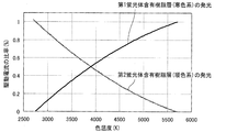
- FIG. 31 is an AA cross-sectional view of the light emitting device shown in FIG. 30. It is a side view which shows one structural example of the LED light bulb which is one Embodiment of this invention. It is a top view of the said LED bulb. It is a figure which shows the color temperature of the said LED bulb with respect to the ratio of the drive current which light-emits the 1st fluorescent substance containing resin layer and the 2nd fluorescent substance containing resin layer. It is a figure which shows the black body radiation locus
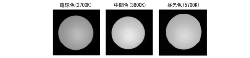
- FIG. 34 shows the color mixture of the light seen through the glove
- a light emitting device using LEDs will be described based on the drawings.
- a light emitting device is provided as a light source in a lighting device such as a general lighting fixture or a TV backlight, and realizes a very excellent lighting device. Further, since the light emitting device uses an LED, energy saving, space saving, and long life can be realized.
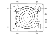
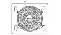
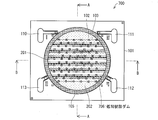
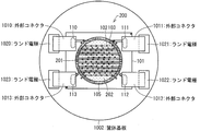
- FIG. 1 is a plan view showing a configuration example of the light emitting device 100 according to the present embodiment.
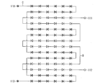
- FIG. 2 is a diagram illustrating a circuit configuration of the LED chip 102 in the light emitting device 100.
- 3 to 6 are plan views showing the configuration of the light emitting device 100 in the manufacturing process.
- FIG. 3 shows a configuration when the electrode wiring pattern and the printed resistance element 104 are formed on the substrate 101.
- FIG. 4 shows a configuration when the LED chip 102 is mounted.
- FIG. 5 shows a configuration when the first resin dam 105 and the second resin dam 106 are formed.
- FIG. 6 shows a configuration when the first phosphor-containing resin layer 107 is formed.
- the light emitting device 100 includes a substrate 101, an LED chip 102 (light emitting element), a printed resistance element 104 (protective element), a first resin dam 105 (resinous frame), and a second resin dam 106 (resin).
- the light emitting device 100 includes a plurality of LED chips 102 electrically connected as shown in FIG.
- two series circuit units in which 26 LED chips 102 are connected in series are mounted. Each series circuit part can be driven independently.
- one of the two series circuit units is referred to as a series circuit unit A, and the other is referred to as a series circuit unit B.
- the substrate 101 is a ceramic substrate made of ceramic.
- the substrate 101 has a rectangular shape in plan view.
- the LED chip 102 On one surface (hereinafter referred to as the upper surface) of the substrate 101, the LED chip 102, the printed resistance element 104, the first resin dam 105, the second resin dam 106, the first phosphor-containing resin layer 107, and the second fluorescence A body-containing resin layer 108 is provided.
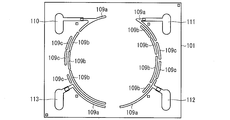
- a power supply wiring 109 and external connection electrode lands 110 to 113 are formed on the top surface of the substrate 101.
- the power supply wiring 109 is not located in the inner region of the first resin dam 105 as much as possible, and the electrical connection between the electrode lands 110 to 113 and the LED chip 102, and between itself and the printed resistance element 104. It is formed so as to have a pattern suitable for connection.
- wirings 109 a to 109 d are formed as the wiring 109.
- the electrode land 110 functions as an anode electrode for the series circuit portion A
- the electrode land 111 functions as a cathode electrode for the series circuit portion A.
- the electrode land 110 is electrically connected to the LED chip 102 located at the highest potential in the series circuit portion A via the wiring 109 a and the wire 103.
- the electrode land 111 is electrically connected to the LED chip 102 located at the lowest potential of the series circuit portion A through the wiring 109 b and the wire 103.
- the electrode land 112 functions as an anode electrode for the series circuit portion B, and the electrode land 113 functions as a cathode electrode for the series circuit portion B.
- the electrode land 112 is electrically connected to the LED chip 102 located at the highest potential in the series circuit portion B via the wiring 109 c and the wire 103.
- the electrode land 113 is electrically connected to the LED chip 102 located at the lowest potential in the series circuit portion B via the wiring 109 d and the wire 103.
- the electrode lands 110 to 113 have an oval shape in plan view.
- the electrode lands 110 to 113 are disposed on the upper surface of the substrate 101 outside the first resin dam 105 and in the vicinity of the four corners on the upper surface.
- the surfaces of the electrode lands 110 to 113 are exposed and can be connected to external terminals.
- the wiring 109a is arranged below the first resin dam 105 on the electrode land 110 arrangement side.
- the wiring 109 a is covered with the first resin dam 105 and extends so that a part thereof overlaps the electrode land 110.
- the wiring 109b is arranged below the first resin dam 105 on the electrode land 111 arrangement side.
- the wiring 109 b is covered with the first resin dam 105, and a part thereof extends toward the center of the upper surface of the substrate, and another part extends so as to overlap the electrode land 111.
- the wiring 109c is arranged below the first resin dam 105 on the electrode land 112 arrangement side.
- the wiring 109 c is covered with the first resin dam 105 and extends so that a part thereof overlaps the electrode land 112.
- the wiring 109d is arranged below the first resin dam 105 on the electrode land 113 arrangement side.
- the wiring 109 d is covered with the first resin dam 105, and a part thereof extends toward the center of the upper surface of the substrate, and another part extends so as to overlap the electrode land 113.
- the LED chip 102 is a blue LED whose emission peak wavelength is around 450 nm.
- the present invention is not limited to this, and as the LED chip 102, for example, an ultraviolet (near-ultraviolet) LED chip having an emission peak wavelength of 390 nm to 420 nm may be used, thereby further improving the light emission efficiency.
- Each LED chip 102 is connected between the LED chips 102 and between the LED chip 102 and the wiring 109 by wires 103 so as to constitute the series circuit portions A and B.
- the series of LED chips 102 in the series circuit part A are arranged so as to draw a spiral (spiral) in plan view (on the spiral).
- the series of LED chips 102 in the series circuit part B are arranged so as to draw a spiral in a plan view between the spiral lines of the series circuit part A and in the same direction as the spirals of the series circuit part A.
- the wire 103 is made of, for example, gold.
- the printing resistance element 104 is provided in two places. One is provided so as to overlap a part of the wiring 109a and a part of the wiring 109b, and is connected in parallel to the series circuit portion A. The other is provided so as to overlap with a part of the wiring 109c and a part of the wiring 109d, thereby being connected in parallel to the series circuit portion B.
- the printed resistance element 104 is disposed below the first resin dam 105 and is covered with the first resin dam 105. Thereby, it is possible to suppress light absorption by the printed resistance element 104.
- the first resin dam 105 and the second resin dam 106 are members that define regions where the first phosphor-containing resin layer 107 and the second phosphor-containing resin layer 108 are formed.
- the first resin dam 105 and the second resin dam 106 function as dams (blocking members) for preventing resin leakage when forming the first phosphor-containing resin layer 107 and the second phosphor-containing resin layer 108. .
- the first resin dam 105 is provided so as to surround a predetermined mounting area of the LED chip 102 (area where a plurality of light emitting portions are formed). Accordingly, the first resin dam 105 has an annular shape (ring shape) in plan view.
- the second resin dam 106 is provided so as to partition the portion surrounded by the first resin dam 105 into a formation region of the first phosphor-containing resin layer 107 and a formation region of the second phosphor-containing resin layer 108.
- the second resin dam 106 includes an area inside the first resin dam 105, an arrangement area of the series of LED chips 102 in the series circuit portion A, and an arrangement area of the series of LED chips 102 in the series circuit portion B.
- it is provided so as to partition without contacting the LED chip 102.
- the 2nd resin dam 106 has a shape which draws a spiral in planar view.
- the first resin dam 105 and the second resin dam 106 are made of a resin having a light reflecting property or a light shielding property, for example, a white silicone resin (a translucent silicone resin is used as a base material, and titanium oxide TiO 2 is used as a light diffusion filler. Etc.). Since the first resin dam 105 and the second resin dam 106 have a light reflecting property or a light shielding property, the light absorption by the first resin dam 105 and the second resin dam 106 is prevented, and the light emission efficiency is lowered. Can be prevented. It is preferable that at least one of a thickener and a diffusing agent is added to the first resin dam 105 and the second resin dam 106.
- the material is not limited to the above material, and the material of the first resin dam 105 and the second resin dam 106 may be acrylic, urethane, epoxy, polyester, acrylonitrile butadiene styrene (ABS), or polycarbonate (PC) resin. Good.
- the 1st resin dam 105 and the 2nd resin dam 106 are colored white, it is not restricted to this, For example, milky white may be sufficient. By coloring the resin white or milky white, the light transmittance of the resin can be set low, or the resin can have light reflectivity.
- the first phosphor-containing resin layer 107 is a sealing resin layer made of a resin containing the first particulate phosphor.
- the first phosphor-containing resin layer 107 is formed so as to fill one region surrounded by the first resin dam 105 and the second resin dam 106 and embed the LED chip 102 and the wire 103 arranged in the region.
- the first phosphor-containing resin layer 107 is formed so as to encapsulate the LED chips 102 of the series circuit portion A and draw a spiral in a plan view.
- the second phosphor-containing resin layer 108 is a sealing resin layer made of a resin containing the second particulate phosphor.
- the second phosphor-containing resin layer 108 is formed so as to fill the other region surrounded by the first resin dam 105 and the second resin dam 106 and to embed the LED chip 102 and the wire 103 arranged in the region.
- the second phosphor-containing resin layer 108 is formed so as to encapsulate the LED chips 102 of the series circuit portion B and draw a spiral in a plan view.
- a Ca 3 (Sc ⁇ Mg) 2 Si 3 O 12 : Ce-based phosphor is used as a green phosphor.
- a (Sr ⁇ Ca) AlSiN 3 : Eu phosphor is used as a red phosphor.
- the region where the first phosphor-containing resin layer 107 is formed becomes a light emitting portion (first light emitting portion) that emits blue light and green light by the “blue LED + green phosphor”.
- the region where the second phosphor-containing resin layer 108 is formed becomes a light emitting portion (second light emitting portion) that emits blue light and red light by “blue LED + red phosphor”.
- FIG. 7 is a flowchart showing the flow of the manufacturing process of the light emitting device 100.
- the manufacturing process of the light emitting device 100 includes an electrode wiring pattern forming process (step S1), a printed resistance element forming process (step S2), an LED chip mounting process (step S3), a first resin dam 2 resin dam formation process (step S4), 1st fluorescent substance content resin layer formation process (step S5), and 2nd fluorescent substance content resin layer formation process (step S6).
- the dimension of each member shown below is only an example, and the light-emitting device 100 is not limited to the dimension.
- wirings 109 a to 109 d and electrode lands 110 to 113 are formed on the upper surface of the substrate 101.
- a substrate 101 having a predetermined size (outside size: 24 mm ⁇ 20 mm, thickness: 1 mm) is prepared.
- a conductor pattern made of gold (Au) is formed on the upper surface of the substrate 101 by printed wiring, thereby forming wirings 109a to 109d (width: 300 ⁇ m, thickness: 10 ⁇ m).
- a conductor pattern made of silver (Ag) -platinum (Pt) is formed on the same surface by printed wiring, so that the electrode lands 110 to 113 (length: 3.5 mm, width: 1.4 mm, thickness: 20 ⁇ m).
- the wirings 109a to 109d and the electrode lands 110 to 113 are formed at predetermined positions.
- the electrode lands 110 and 111 are a pair of anode / cathode electrodes corresponding to the series circuit portion A
- the electrode lands 112 and 113 are a pair of anode / cathode electrodes corresponding to the series circuit portion B. Can be easily recognized.
- the printed resistance element 104 is formed on the upper surface of the substrate 101. Specifically, after a paste containing a resistance component is screen-printed, the substrate 101 is baked in an electric furnace to fix the paste, whereby the printing resistance element 104 (width: 0.2 ⁇ m, thickness: 10 ⁇ m, resistance value) : 1 M ⁇ ).
- the paste is composed mainly of ruthenium oxide (RuO 2 ).
- RuO 2 ruthenium oxide
- the formation order may be reversed.
- the order of forming the wirings 109a to 109d and the electrode lands 110 to 113 may be reversed. It can be formed in a suitable order in consideration of work efficiency and the like.
- the LED chip 102 is mounted on the upper surface of the substrate 101. Specifically, first, 52 LED chips 102 are die-bonded at predetermined positions (from the outside toward the center) using, for example, silicone resin.
- the LED chip 102 has a rectangular shape in plan view (width: 360 ⁇ m, length: 440 ⁇ m, height: 80 ⁇ m). Two chip electrodes for the anode and the cathode are provided on the rectangular upper surface of the LED chip 102.
- wire bonding is performed using the wire 103 so that the circuit configuration shown in FIG. 2 and the series of connected LED chips 102 draw a spiral.
- the wiring 109a and the chip electrode of the LED chip 102 are connected by the wire 103
- the chip electrodes of the adjacent LED chips 102 are connected by the wire 103
- the chip electrode of the LED chip 102 and the wiring 109b are connected.
- the wiring 109c and the chip electrode of the LED chip 102 are connected by the wire 103
- the chip electrodes of the adjacent LED chips 102 are connected by the wire 103
- the chip electrode of the LED chip 102 and the wiring 109d are connected.
- the 26 LED chips 102 are connected in series between the electrode land 110 and the electrode land 111, and the series circuit portion A arranged in a spiral shape is configured.
- 26 LED chips 102 are connected in series between the electrode land 112 and the electrode land 113 to form a series circuit portion B arranged in a spiral shape.
- FIG. 4 shows a state after the LED chip mounting process is completed.
- the first resin dam 105 and the second resin dam 106 are formed on the upper surface of the substrate 101.
- a liquid white silicone resin (containing the light diffusion filler TiO 2 ) is drawn at a predetermined position using a dispenser. That is, after drawing at the formation position of the first resin dam 105, drawing is performed at the formation position of the second resin dam 106. At this time, the start point of the formation of the second resin dam 106 is in contact with the first resin dam 105, and the end point thereof is also in contact with the first resin dam 105. The second resin dam 106 is not brought into contact with the LED chip 102.
- the first resin dam 105 (width: 1 mm, ring diameter: 16 mm) and the second resin dam 106 (width: 0.5 mm) are formed by thermosetting under conditions of temperature: 150 ° C. and time: 60 minutes. To do.
- said temperature and time are examples, and are not limited to this.
- FIG. 5 shows a state after the first resin dam / second resin dam formation step is completed.
- the first resin dam 105 thus formed covers a part of the wirings 109a to 109d.
- the second resin dam 106 covers a part of the wirings 109b and 109d. Therefore, light absorption by the wirings 109a to 109d can be suppressed.
- the first resin dam 105 and the second resin dam 106 are formed in the order after the LED chip 102 is mounted. Conversely, the first resin dam 105 and the second resin dam 106 are formed. Later, the order of mounting the LED chips 102 may be adopted. Each process can be performed in a suitable order in consideration of work efficiency and the like.
- a first phosphor-containing resin layer 107 is formed on the upper surface of the substrate 101.
- a fluorescent particle-containing resin in which a first particulate phosphor is dispersed in a liquid transparent silicone resin is placed in one region surrounded by the first resin dam 105 and the second resin dam 106. Inject to fill.
- the first phosphor-containing resin layer 107 is formed by thermosetting under conditions of temperature: 150 ° C. and time: 30 minutes.
- said temperature and time are examples, and are not limited to this.
- the first phosphor-containing resin layer 107 is formed at a predetermined position. That is, the first phosphor-containing resin layer 107 is formed so as to encapsulate the LED chips 102 of the series circuit portion A and draw a spiral in a plan view.
- FIG. 6 shows a state after the first phosphor-containing resin layer forming step is completed.
- a second phosphor-containing resin layer 108 is formed on the upper surface of the substrate 101.
- a fluorescent particle-containing resin obtained by dispersing a second particulate phosphor in a liquid transparent silicone resin is used for the other region surrounded by the first resin dam 105 and the second resin dam 106. Inject to fill.
- the second phosphor-containing resin layer 108 is formed by thermosetting under conditions of temperature: 150 ° C. and time: 5 hours.
- the second phosphor-containing resin layer 108 is formed at a predetermined position. That is, the second phosphor-containing resin layer 108 is formed so as to encapsulate the LED chips 102 of the series circuit portion B and draw a spiral in a plan view.
- the light emitting device 100 shown in FIG. 1 can be manufactured.
- the light emitting device 100 by connecting an external terminal to the electrode lands 110 to 113 and supplying electric power, light emission from the first phosphor-containing resin layer 107 and light emission from the second phosphor-containing resin layer 108 are achieved. Can be driven independently.
- the first phosphor-containing resin layer 107 and the second phosphor-containing resin layer 108 are provided in the region partitioned by the second resin dam 106, so that the respective light emitting surfaces are close to each other. ing. Further, the boundary portion (spiral shape) of each light emitting surface is present substantially uniformly over the entire inner region of the first resin dam 105. Therefore, when the light source is viewed directly, it becomes easy to see as one light emission point with mixed colors, and it becomes possible to make it difficult to recognize the separation between the light emission point and the light emission color.
- the light emitting device 100 includes the LED chip 102 and the first phosphor-containing resin layer 107 of the series circuit portion A in two spiral regions surrounded by the first resin dam 105 and the second resin dam 106. And a second light-emitting portion formed by the LED chip 102 and the second phosphor-containing resin layer 108 of the series circuit portion B are formed. .
- the first light emitting unit emits blue light and green light by “blue LED + green phosphor”.
- the second light emitting unit emits blue light and red light by “blue LED + red phosphor”. Therefore, the light emitting device 100 emits white light by mixing blue light, green light, and red light.
- electrode lands 110 and 111 electrically connected to the LED chip 102 of the first light emitting unit and electrode lands 112 and 113 electrically connected to the LED chip 102 of the second light emitting unit are used.
- the first light emitting unit and the second light emitting unit can be individually driven.
- each light emitting part can be driven individually, each light emitting part can be turned on individually, or each light emission can be adjusted by adjusting the lighting condition (light emission intensity) of each light emitting part. It is possible to easily adjust the light emission of the entire light emitting device, which is a color mixture of the light emission from the section, so as to have a desired chromaticity.
- each light emitting part is formed not in a shape gathered in one place but in a complicated shape called a spiral. Therefore, since the same light distribution characteristics are intricately close to each other, it is easy to obtain a color mixture when the light emitting units are simultaneously turned on, and a very good color mixture is possible. Furthermore, since each light emitting part is close, the influence of heat on each light emitting part is the same, the brightness and color tone of the generated white light is less affected by heat and changes over time, It becomes possible to reduce fluctuations in peak wavelength and large color rendering properties.
- each light emitting unit is configured to emit at least one color different from each other, thereby obtaining light emission by mixing at least two colors. Therefore, since it is possible to easily adjust the light emission chromaticity of the light emitting device as a whole, high color rendering properties can be easily obtained depending on the combination of colors emitted by the light emitting units.
- the light emitting device 100 it is possible to obtain a further color mixing property as compared with the conventional case, and it is possible to easily achieve light emission with high color rendering properties with easy color adjustment.
- the printed resistance element 104 is arranged in parallel with the LED chip 102 connected between the electrode lands 110 and 111, and the LED chip connected between the electrode lands 112 and 113. 102 is connected in parallel with 102. As a result, it is possible to prevent the LED chip 102 from being deteriorated, and it is possible to extend the life and ensure the reliability.
- the printed resistance element 104 and most of the wiring 109 are formed below the first resin dam 105.
- the first resin dam 105 can protect the printed resistance element 104 and the wiring 109 from the outside. Furthermore, since the lower portion of the first resin dam 105 is effectively used, the light emitting device 100 can be downsized even if the printed resistance element 104 is mounted.
- one light emitting unit is not limited to the number of LED chips 102 illustrated in FIG. 1, but may include a plurality of LED chips 102.
- the plurality of LED chips 102 constituting the light emitting unit are not limited to being connected in series, but may be connected in parallel or may be configured in series-parallel connection.
- the wiring 109 can be formed at a suitable position according to the circuit configuration of the LED chip 102.
- the electrode lands 110 to 113 can be set to function as an anode electrode or a cathode electrode depending on the direction of polarity when the LED chip 102 is disposed.
- the number of light emitting units is not limited to two, and can be three or more. What is necessary is just to change the number which the 2nd resin dam 106 partitions according to the number of the light emission parts.
- the cathode electrode the same number of electrode lands as the light emitting portions may be used, or one electrode land may be shared (integrated).
- the first particulate phosphor is not limited to the green phosphor
- the second particulate phosphor is not limited to the red phosphor.
- the first particulate phosphor and the second particulate phosphor are phosphors that obtain light emission of a predetermined color (chromaticity) from the light emitting device 100 in combination with the emission color of the LED chip 102, Different phosphors may be used.
- each light emitting unit may be configured such that at least two light emitting units emit at least one color different from each other.
- At least one of the light emitting units has at least a blue wavelength. It is desirable that at least one light emitting unit that emits blue light having a spectrum and yellow light having a yellow wavelength spectrum emits red light having at least a red wavelength spectrum.
- white light generated by a mixture of blue light and yellow light is a pseudo white light with a yellowish color overall because the red light emitting component is poor.
- it is possible to adjust the ratio of the addition of the pseudo white light and the red light so that the red light emission component is increased and the white light with the suppressed color deviation can be easily obtained. Can be obtained. Further, by increasing the amount of red light, it is possible to generate warm mixed color (bulb color) light.
- each light-emitting portion may be made of a light-transmitting resin that does not contain a phosphor, depending on the emission color of the entire light-emitting device.
- the sealing resin layer of each light emitting part is any one of a translucent resin containing one type of phosphor, a translucent resin containing a plurality of types of phosphors, and a translucent resin not containing phosphors. Can be configured. Further, the phosphor content may be different for each light emitting part.
- the second resin dam 106 is formed so as to draw a spiral in a plan view, whereby the shape of each light emitting portion is spiral.
- the shape of each light emitting portion is not limited to such a shape, for example, a spiral shape in which a linear portion is partially mixed, a shape in which the linear portion is bent and converges from the outside to the center, etc. can do.
- the second resin dams 106 (boundary portions) between the adjacent light emitting portions may be formed in one piece so that the formation regions of the respective light emitting portions have the shapes described above in plan view.
- each light emitting portion that can be provided with two or more is the above reference when the center of the formation region of the plurality of light emitting portions on the top surface is a reference point when viewed from the direction perpendicular to the top surface of the substrate 101.
- the phosphor-containing resin layer of each light-emitting part is set so as to be disposed at a plurality of locations so as to be adjacent to the phosphor-containing resin layer of a different light-emitting part. It only has to be. Thereby, the above-described excellent color mixing property can be obtained.
- the planar shape of the first resin dam 105 is not limited to an annular shape, and may be a polygonal shape or a polygonal annular shape with rounded corners.
- the light emitting area of the light emitting device 100 as a whole when all the LED chips 102 are turned on at the same time is circular, and light emission is easily emitted uniformly in all directions. Thereby, it becomes easy to apply the light-emitting device 100 to a general-purpose lighting fixture and to design the same.
- the LED chips 102 having the same shape are mounted, but the present invention is not limited to this, and LEDs having different shapes and sizes may be appropriately mounted.
- the upper surface of the LED chip 102 is not limited to a rectangle but may be a square. Thereby, the freedom degree of arrangement
- the shape of the upper surface of the substrate 101 is not limited to a rectangle, but may be a square or a circle.
- a substrate made of ceramic is used as the substrate 101.
- the present invention is not limited to this, and instead of the ceramic substrate, for example, a metal core substrate having an insulating layer formed on the metal substrate surface is used. May be.
- the insulating layer can be formed only in an area where the printed resistance element 104, the wiring 109, and the electrode lands 110 to 113 are formed, and the plurality of LED chips 102 can be directly mounted on the surface of the metal substrate. .
- the printed resistance element 104 is formed for protecting the LED chip 102
- a Zener diode (protective element) may be provided instead of the printed resistance element 104.
- the printed resistance element 104 and the Zener diode are preferably covered with the first resin dam 105 as much as possible, but this is not restrictive.
- the light emitting device 100 is not necessarily provided with the printed resistance element 104.
- the size (resistance value) of the printed resistance element 104 and circuit installation depend on the number of LED chips 102 to be mounted and the usage environment (size of electrostatic withstand voltage that may be applied to the LED chip 102, etc.). Can be decided.
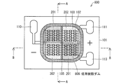
- FIG. 8 is a plan view showing a configuration example of the light-emitting device 200 of the present embodiment.
- FIG. 9 is a diagram illustrating a circuit configuration of the LED chip 102 in the light emitting device 200.
- 10 to 13 are plan views showing the configuration of the light emitting device 200 in the manufacturing process.
- FIG. 10 shows a configuration when an electrode wiring pattern is formed on the substrate 101.
- FIG. 11 shows a configuration when the LED chip 102 is mounted.
- FIG. 12 shows a configuration when the first resin dam 105 is formed.
- FIG. 13 shows a configuration when the first phosphor-containing resin layer 201 is formed.
- the light emitting device 200 includes a substrate 101, an LED chip 102, a first resin dam 105, a first phosphor-containing resin layer 201 (resin layer), and a second phosphor-containing resin layer 202 (resin layer). ).
- the light emitting device 200 includes a plurality of LED chips 102 that are electrically connected as shown in FIG.
- a series circuit unit in which 48 LED chips 102 are connected in series and a series circuit unit in which 36 LED chips 102 are connected in series are mounted.
- Each series circuit part can be driven independently.
- a series circuit unit including 48 LED chips 102 is referred to as a series circuit unit C
- a series circuit unit including 36 LED chips 102 is referred to as a series circuit unit D.
- the LED chip 102, the first resin dam 105, the first phosphor-containing resin layer 201, and the second phosphor-containing resin layer 202 are provided on the upper surface of the substrate 101.
- the wirings 109a to 109c on the substrate 101 have a pattern for realizing the circuit configuration shown in FIG. Specifically, as shown in FIG. 10, the wiring 109a is an electrode wiring pattern connected to the electrode lands 110 to 113.
- the wiring 109b is a relay wiring pattern for relaying the wire 103 constituting the series circuit portion C and electrically connecting the LED chips 102, and the wiring 109c is a wire constituting the series circuit portion D. This is a relay wiring pattern for relaying 103 and electrically connecting the LED chips 102.
- the electrode land 113 functions as an anode electrode for the series circuit portion C
- the electrode land 110 functions as a cathode electrode for the series circuit portion C.
- the electrode land 113 is electrically connected to the LED chip 102 located at the highest potential of the series circuit portion C via the wiring 109 a and the wire 103.
- the electrode land 110 is electrically connected to the LED chip 102 located at the lowest potential of the series circuit portion C via the wiring 109 a and the wire 103.
- the electrode land 111 functions as an anode electrode for the series circuit portion D
- the electrode land 112 functions as a cathode electrode for the series circuit portion D.
- the electrode land 111 is electrically connected to the LED chip 102 located at the highest potential of the series circuit portion D via the wiring 109 b and the wire 103.
- the electrode land 112 is electrically connected to the LED chip 102 located at the lowest potential of the series circuit portion D through the wiring 109b and the wire 103.
- the wirings 109 a to 109 c are arranged below the first resin dam 105.
- the wiring 109 a is covered with the first resin dam 105 and extends so as to partially overlap the electrode lands 110 to 113. In the region inside the first resin dam 105, the wirings 109a to 109c are not arranged.
- the LED chips 102 are connected by wires 103 between the LED chips 102 and between the LED chips 102 and the wiring 109 so as to constitute a series circuit portion CD.
- the series of LED chips 102 in the series circuit portion C is arranged so that six LED chips 102 in one row (row direction, x direction) are arranged in eight rows in the column direction (y direction).
- a series of LED chips 102 in the series circuit portion D are arranged in six lines in three places between the second and third rows of the series circuit portion C, between the fourth and fifth rows, and between the sixth and seventh rows.
- LED chips 102 are arranged in two rows. That is, in the light emitting device 200, the LED chips 102 of the series circuit unit C and the LED chips 102 of the series circuit unit D are alternately arranged in two rows in the column direction.
- the columns of the six LED chips 102 are electrically connected by the wires 103 and the wirings 109b.
- the columns of the six LED chips 102 are electrically connected by wires 103 and wires 109c.
- a first phosphor-containing resin layer 201 and a second phosphor-containing resin layer 202 are formed in a region inside the first resin dam 105.
- the first phosphor-containing resin layer 201 is a sealing resin layer made of a resin containing the first particulate phosphor.
- the first phosphor-containing resin layer 201 is a region inside the first resin dam 105 and is formed so as to bury the LED chip 102 and the wire 103 of the series circuit portion D disposed in the region. That is, the 1st fluorescent substance content resin layer 201 is formed so that LED chip 102 of series circuit part D may be divided into a plurality of groups, and may be sealed, respectively. Thereby, the 1st fluorescent substance containing resin layer 201 is formed in three places in strip
- the second phosphor-containing resin layer 202 is a sealing resin layer made of a resin containing the second particulate phosphor.
- the second phosphor-containing resin layer 202 is an area inside the first resin dam 105 and is formed so as to bury the LED chip 102 and the wire 103 of the series circuit portion C disposed in the area. That is, the 2nd fluorescent substance content resin layer 202 is formed so that LED chip 102 of series circuit part C may be divided into a plurality of groups, and may be sealed, respectively. Thereby, the 2nd fluorescent substance containing resin layer 202 is formed in four places in strip
- the first phosphor-containing resin layer 201 and the second phosphor-containing resin layer 202 form a stripe pattern (here, a horizontal stripe) in the region inside the first resin dam 105 in a plan view.
- a (Sr ⁇ Ca) AlSiN 3 : Eu-based phosphor is used as a red phosphor having a peak emission wavelength in the vicinity of 630 nm.
- the second particulate phosphor includes a Ca 3 (Sc ⁇ Mg) 2 Si 3 O 12 : Ce phosphor as a green phosphor having a peak emission wavelength near 520 nm, and a red having a peak emission wavelength near 620 nm.
- phosphors two types of phosphors, (Sr ⁇ Ca) AlSiN 3 : Eu-based phosphors, are used.
- the region where the first phosphor-containing resin layer 201 is formed becomes a light emitting portion (first light emitting portion) that emits blue light and red light by the “blue LED + red phosphor”.
- the region where the second phosphor-containing resin layer 202 is formed becomes a light emitting portion (second light emitting portion) that emits blue light, green light, and red light by “blue LED + green phosphor + red phosphor”.
- the light emitting device 200 having the above configuration can be performed in the same order as the method for manufacturing the light emitting device 100 of the first embodiment described with reference to FIG.
- the manufacturing process of the light emitting device 200 includes an electrode wiring pattern forming process (corresponding to step S1 in FIG. 7), an LED chip mounting process (corresponding to step S3 in FIG. 7), and a first resin dam forming process (corresponding to step S1 in FIG. 7).
- Step S4 a first phosphor-containing resin layer forming step (corresponding to Step S5 in FIG. 7), and a second phosphor-containing resin layer forming step (corresponding to Step S6 in FIG. 7).
- the dimension of each member shown below is only an example, and the light-emitting device 100 is not limited to the dimension.
- FIG. 10 shows a state after the electrode wiring pattern forming process is completed.
- the LED chip 102 is mounted on the upper surface of the substrate 101. Specifically, first, 84 LED chips 102 are die-bonded at predetermined positions using, for example, silicone resin.
- wire bonding is performed using the wire 103 so that the circuit configuration shown in FIG. 9 and the wire 103 are laid in the row direction. That is, the LED chip 102 and the wirings 109 a to 109 c and the LED chips 102 are sequentially connected by the wire 103.
- FIG. 11 shows a state after the LED chip mounting process is completed.
- FIG. 12 shows a state after the first resin dam formation process is completed.
- the first resin dam 105 thus formed covers almost the entire area of the wirings 109a to 109c. Further, the wirings 109 a to 109 c are not formed in the inner region of the first resin dam 105. Therefore, light absorption by the wirings 109a to 109c can be significantly suppressed.
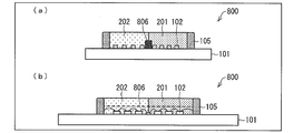
- a first phosphor-containing resin layer 201 is formed on the upper surface of the substrate 101.
- the first phosphor-containing resin layer 201 is formed by placing a resin containing fluorescent particles, in which a red phosphor is dispersed in a transparent silicone resin, on a predetermined position.
- the silicone resin of the first phosphor-containing resin layer 201 was formed of a resin having high thixotropy and no fluidity.
- the thixotropy is a physical property in which a high-viscosity state is a normal state, and when this is agitated, the state becomes a torsional state only during that time. For example, it can be realized by mixing a thixotropic additive into the resin.
- the first phosphor-containing resin layer 201 is not cured by heat after being placed on the upper surface of the substrate 101, and the viscosity is increased and solidified during viewing.
- the 1st fluorescent substance content resin layer 201 seals LED chip 102 of series circuit part D, and is formed in a belt shape by plane view.
- the first phosphor-containing resin layer 201 is made of a resin having a higher thixotropy (higher viscosity) than the second phosphor-containing resin layer 202, so that the first phosphor-containing resin layer 201 can be changed at the present time. There is no need to heat cure.
- the first phosphor-containing resin layer 201 is a so-called resin dam (resin wall) for forming the second phosphor-containing resin layer 202. That is, the first phosphor-containing resin layer 201 can be used as a dam material without being cured.
- a second phosphor-containing resin layer 202 is formed between the first phosphor-containing resin layers 201.
- FIG. 13 shows a state after the first phosphor-containing resin layer forming step is completed. The first phosphor-containing resin layer 201 is completely cured by the thermosetting process when forming the second phosphor-containing resin layer 202.
- a second phosphor-containing resin layer 202 is formed on the upper surface of the substrate 101.
- a region surrounded by a first resin dam 105 and a first phosphor-containing resin layer 201 is a resin containing fluorescent particles obtained by dispersing a second particulate phosphor in a liquid transparent silicone resin. Inject to fill (4 places in total).
- the second phosphor-containing resin layer 202 is formed by thermosetting under conditions of temperature: 150 ° C. and time: 5 hours. At this time, the first phosphor-containing resin layer 201 is simultaneously cured.
- the second phosphor-containing resin layer 202 is formed at a predetermined position. That is, the second phosphor-containing resin layer 202 is formed in a band shape in plan view by sealing the LED chip 102 of the series circuit portion C. Further, the first phosphor-containing resin layer 201 is also completely formed.
- the light emitting device 200 shown in FIG. 8 can be manufactured.
- the light emitting device 200 by connecting an external terminal to the electrode lands 110 to 113 and supplying electric power, light emission from the first phosphor-containing resin layer 201 and light emission from the second phosphor-containing resin layer 202 are achieved. Can be driven independently.
- the first phosphor-containing resin layer 201 and the second phosphor-containing resin layer 202 are in contact with each other, so that the respective light emitting surfaces are close to each other.
- the boundary portion (stripe shape) of each light emitting surface is the first.
- the light-emitting device 200 is connected in series with the first light-emitting unit configured by the LED chip 102 of the series circuit unit D and the first phosphor-containing resin layer 201 in the region inside the first resin dam 105.
- the LED part 102 of the circuit part C and the 2nd light emission part comprised by the 2nd fluorescent substance containing resin layer 202 are each formed.
- the first light emitting unit emits blue light and red light by “blue LED + red phosphor”.
- the second light emitting unit emits blue light, green light, and red light by “blue LED + green phosphor + red phosphor”. Therefore, the light emitting device 100 emits white light by mixing blue light, green light, and red light.
- the electrode lands 111 and 112 electrically connected to the LED chip 102 of the first light emitting unit and the electrode lands 110 and 113 electrically connected to the LED chip 102 of the second light emitting unit are used.
- the first light emitting unit and the second light emitting unit can be individually driven.
- each light emitting part can be driven individually, each light emitting part can be turned on individually, or each light emission can be adjusted by adjusting the lighting condition (light emission intensity) of each light emitting part. It is possible to easily adjust the light emission of the entire light emitting device, which is a color mixture of the light emission from the section, so as to have a desired chromaticity.
- each light emitting part is not a shape gathered in one place, but is formed in an intricate shape such as a stripe shape in which the light emitting parts are alternately arranged (switched at a short distance). Therefore, since the same light distribution characteristics are intricately close to each other, it is easy to obtain a color mixture when the light emitting units are simultaneously turned on, and a very good color mixture is possible. Furthermore, since each light emitting part is close, the influence of heat on each light emitting part is the same, the brightness and color tone of the generated white light is less affected by heat and changes over time, It becomes possible to reduce fluctuations in peak wavelength and large color rendering properties.
- each light emitting unit is configured to emit at least one color different from each other, thereby obtaining light emission by mixing at least two colors. Therefore, since it is possible to easily adjust the light emission chromaticity of the light emitting device as a whole, high color rendering properties can be easily obtained depending on the combination of colors emitted by the light emitting units.
- the light emitting device 200 it is possible to obtain a further color mixing property as compared with the conventional case, and it is possible to easily realize light emission with high color rendering with easy color adjustment.
- the number of light emitting units is not limited to two, and may be three or more.
- Each light-emitting part that can be provided with two or more is formed so that the plurality of phosphor-containing resin layers in each light-emitting part are not adjacent to the phosphor-containing resin layer of the same light-emitting part and are arranged in a striped pattern. It only has to be done.
- the first phosphor-containing resin layer 201 has a higher refractive index than the second phosphor-containing resin layer 202.
- the first phosphor-containing resin layer 201 having a refractive index higher than that of the second phosphor-containing resin layer 202, the first phosphor-containing resin is removed from the LED chip 102 sealed in the second phosphor-containing resin layer 202.
- the light emitted in the direction in which the layer 201 exists is reflected by the first phosphor-containing resin layer 201.
- the second phosphor-containing resin layer 202 has a lower thixotropy than the first phosphor-containing resin layer 201. It may be a fluid property. Since the first phosphor-containing resin layer 201 becomes a resin dam (resin wall), the first phosphor-containing resin layer 201 and the second phosphor-containing resin layer 202 are not mixed. In other words, the boundary surface of each resin layer is almost clear.
- the resin layer made of resin having no thixotropy (a range that can be regarded as almost zero) is set so as not to be adjacent. Thereby, the resin layer of each light emission part can be formed in a predetermined location, without mixing with the resin layer of another light emission part.
- the first phosphor-containing resin layer 201 and the second phosphor-containing resin layer 202 are in direct contact as described above, but the second resin described in the first embodiment is used.
- a configuration using a dam 106 may also be used.
- the 2nd resin dam 106 After forming the 2nd resin dam 106 in the boundary part between light emission parts, what is necessary is just to form the 1st fluorescent substance containing resin layer 201 and the 2nd fluorescent substance containing resin layer 202 one by one. . At this time, it is not necessary to use a thixotropic resin.
- the light emitting device 100 of the first embodiment can also be configured such that the second resin dam 106 and further the first resin dam 105 are not used by using a thixotropic resin.
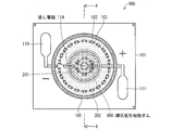
- FIG. 14 is a plan view illustrating a configuration example of the light emitting device 300 according to the present embodiment.
- FIG. 15 is a diagram illustrating a circuit configuration of the LED chip 102 in the light emitting device 300.
- FIG. 16 is a plan view showing a configuration when the LED chip 102 is mounted in the manufacturing process of the light emitting device 300.
- the light emitting device 300 of the present embodiment has the same configuration as the light emitting device 200 of the above embodiment except for the following configuration.
- the light emitting device 300 includes a plurality of LED chips 102 electrically connected as shown in FIG.
- a serial-parallel circuit unit in which 48 LED chips 102 are connected in series and parallel (6 series ⁇ 2 parallel 4 series) and 36 LED chips 102 are connected in series and parallel (6 series ⁇ 2).
- a series-parallel circuit unit in which three series are connected in parallel.
- the series-parallel circuit unit including the 48 LED chips 102 is referred to as a series-parallel circuit unit E
- the series-parallel circuit unit including the 36 LED chips 102 is referred to as a series-parallel circuit unit F.
- the wiring 109 of the substrate 101 has a pattern as clearly shown in FIG.
- the LED chips 102 are connected by wires 103 between the LED chips 102 and between the LED chips 102 and the wiring 109 so as to constitute the series-parallel circuit portions E and F.
- the arrangement of the LED chip 102 is almost the same as the arrangement of the LED chip 102 of the light emitting device 200.
- the first phosphor-containing resin layer 201 is formed so that the LED chips 102 of the series-parallel circuit part F are divided into a plurality of groups and sealed (three places).
- the 2nd fluorescent substance content resin layer 202 is formed so that LED chip 102 of series parallel circuit part E may be divided into a plurality of groups, and may be sealed, respectively (four places). Therefore, the first phosphor-containing resin layer 201 and the second phosphor-containing resin layer 202 form a striped pattern in a region inside the first resin dam 105 in plan view.
- a CaAlSiN 3 : Eu-based phosphor is used as a red phosphor having a peak emission wavelength near 650 nm.
- the second particulate phosphor includes a Ca 3 (Sc ⁇ Mg) 2 Si 3 O 12 : Ce phosphor as a green phosphor having a peak emission wavelength near 520 nm, and a red having a peak emission wavelength near 630 nm.
- phosphors two types of phosphors, (Sr ⁇ Ca) AlSiN 3 : Eu-based phosphors, are used.
- the region where the first phosphor-containing resin layer 201 is formed becomes a light emitting portion (first light emitting portion) that emits blue light and red light by the “blue LED + red phosphor”.
- the region where the second phosphor-containing resin layer 202 is formed becomes a light emitting portion (second light emitting portion) that emits blue light, green light, and red light by “blue LED + green phosphor + red phosphor”.
- the LED chips 102 are connected in parallel. Specifically, in each region where the first phosphor-containing resin layer 201 is formed and in each region where the second phosphor-containing resin layer 202 is formed, six LED chips 102 in series and two in parallel are sealed. It has been stopped. As a result, even if any one of the LED chips 102 is damaged, it is possible to avoid a situation in which all the LED chips 102 stop emitting light.
- FIG. 17 is a plan view illustrating a configuration example of the light-emitting device 400 of the present embodiment.
- FIG. 18 is a diagram illustrating a circuit configuration of the LED chip 102 in the light emitting device 400.
- FIG. 19 is a plan view showing a configuration when the LED chip 102 is mounted in the manufacturing process of the light emitting device 400.
- the light emitting device 400 of the present embodiment has the same configuration as the light emitting device 200 of the second embodiment except for the following configuration.
- the light emitting device 400 includes a plurality of LED chips 102 that are electrically connected as shown in FIG.
- a serial-parallel circuit unit in which 48 LED chips 102 are connected in series and parallel (6 series ⁇ 8 parallel) and 36 LED chips 102 are connected in series and parallel (6 series ⁇ 6 parallel).
- a series-parallel circuit section in which 48 LED chips 102 are connected in series and parallel (6 series ⁇ 8 parallel) and 36 LED chips 102 are connected in series and parallel (6 series ⁇ 6 parallel).
- a series-parallel circuit section The cathode electrode of each series-parallel circuit part is shared.
- the series-parallel circuit unit including 48 LED chips 102 is referred to as a series-parallel circuit unit G
- the series-parallel circuit unit including 36 LED chips 102 is referred to as a series-parallel circuit unit H.
- the wiring 109 of the substrate 101 has a pattern as clearly shown in FIG. Furthermore, the LED chips 102 are connected by wires 103 between the LED chips 102 and between the LED chips 102 and the wirings 109 so as to constitute the series-parallel circuit portions G and H.
- the arrangement of the LED chip 102 is almost the same as the arrangement of the LED chip 102 of the light emitting device 200.
- the light emitting device 400 includes a printed resistance element 104.
- the print resistance element 104 is provided at two places as clearly shown in FIG. One is connected in parallel to the series-parallel circuit unit G, and the other is connected in parallel to the series-parallel circuit unit H.
- the first phosphor-containing resin layer 201 is formed so that the LED chips 102 of the series-parallel circuit portion H are divided into a plurality of groups and sealed (three places).
- the 2nd fluorescent substance content resin layer 202 is formed so that LED chip 102 of series parallel circuit part G may be divided into a plurality of groups, and may be sealed, respectively (four places). Therefore, the first phosphor-containing resin layer 201 and the second phosphor-containing resin layer 202 form a striped pattern in a region inside the first resin dam 105 in plan view.
- the first particulate phosphor of the first phosphor-containing resin layer 201 As a green phosphor having a peak emission wavelength near 520 nm, a Ca 3 (Sc ⁇ Mg) 2 Si 3 O 12 : Ce phosphor, As a red phosphor (first red phosphor) having a peak emission wavelength in the vicinity of 630 nm, two types of phosphors of (Sr ⁇ Ca) AlSiN 3 : Eu-based phosphor are used.
- the second particulate phosphor includes a Ca 3 (Sc ⁇ Mg) 2 Si 3 O 12 : Ce phosphor as a green phosphor having a peak emission wavelength near 520 nm, and a red having a peak emission wavelength near 620 nm.
- a phosphor (second red phosphor) two types of phosphors, (Sr ⁇ Ca) AlSiN 3 : Eu phosphor, are used.
- the region where the first phosphor-containing resin layer 201 is formed is a light emitting unit (first light emitting unit) that emits blue light, green light, and red light by “blue LED + green phosphor + red phosphor”.
- the region where the second phosphor-containing resin layer 202 is formed becomes a light emitting portion (second light emitting portion) that emits blue light, green light, and red light by “blue LED + green phosphor + red phosphor”.
- Color rendering properties and emission intensity can be controlled by using two kinds of red phosphors having a peak emission wavelength in a large long wavelength region. Therefore, by using two types of red phosphors, the emission spectrum of the red component can be broadened, and thus high color rendering can be realized. In addition, by using two types of red phosphors, high color rendering can be achieved while maintaining luminous efficiency.
- FIG. 20 is a plan view showing a configuration example of the light emitting device 500 of the present embodiment.
- FIG. 21 is a diagram illustrating a circuit configuration of the LED chip 102 in the light emitting device 500.
- FIG. 22 is a plan view showing a configuration when the LED chip 102 is mounted in the manufacturing process of the light emitting device 500.
- the light emitting device 500 of the present embodiment has the same configuration as the light emitting device 200 of the second embodiment except for the following configuration.
- the light emitting device 500 includes a plurality of LED chips 102 that are electrically connected as shown in FIG.
- a serial / parallel circuit unit in which 48 LED chips 102 are connected in series and parallel (6 series ⁇ 8 parallel) and 36 LED chips 102 are connected in series and parallel (6 series ⁇ 6 parallel).
- a series-parallel circuit section a series-parallel circuit unit J
- the series-parallel circuit unit including 36 LED chips 102 is referred to as a series-parallel circuit unit K.
- the wiring 109 of the substrate 101 has a pattern as clearly shown in FIG. Furthermore, the LED chips 102 are connected by wires 103 between the LED chips 102 and between the LED chips 102 and the wiring 109 so as to constitute a series-parallel circuit portion J ⁇ K.
- the arrangement of the LED chip 102 is almost the same as the arrangement of the LED chip 102 of the light emitting device 200.
- the light emitting device 500 includes a printed resistance element 104.
- the print resistance elements 104 are provided at two locations as clearly shown in FIG. One is connected in parallel to the series-parallel circuit unit J, and the other is connected in parallel to the series-parallel circuit unit K.
- the first phosphor-containing resin layer 201 is formed so that the LED chips 102 of the series-parallel circuit portion K are divided into a plurality of groups and sealed (three places).
- the 2nd fluorescent substance content resin layer 202 is formed so that LED chip 102 of series parallel circuit part J may be divided into a plurality of groups, and may be sealed, respectively (four places). Therefore, the first phosphor-containing resin layer 201 and the second phosphor-containing resin layer 202 form a striped pattern in a region inside the first resin dam 105 in plan view.
- a Ca 3 (Sc ⁇ Mg) 2 Si 3 O 12 : Ce phosphor is used as the green phosphor.
- a CaAlSiN 3 : Eu phosphor is used as a red phosphor.
- the region where the first phosphor-containing resin layer 201 is formed becomes a light emitting portion (first light emitting portion) that emits blue light and green light by the “blue LED + green phosphor”.
- the region where the second phosphor-containing resin layer 202 is formed becomes a light emitting portion (second light emitting portion) that emits blue light and red light by “blue LED + red phosphor”.
- FIG. 24 is a plan view illustrating a configuration example of the light-emitting device 600 of the present embodiment.
- FIG. 25 is a cross-sectional view taken along line AA of the light emitting device 600 of FIG.
- the light emitting device 600 of the present embodiment includes a first phosphor-containing resin in place of the first phosphor-containing resin layer 201 and the second phosphor-containing resin layer 202 in the configuration of the light-emitting device 200 of the second embodiment.
- a layer 601 and a second phosphor-containing resin layer 602 are provided. That is, as shown in FIG. 24, the light emitting device 600 includes a substrate 101, an LED chip 102, a first resin dam 105, a first phosphor-containing resin layer 601 (resin layer), and a second phosphor-containing resin layer 602. (Resin layer).
- the LED chip 102, the first resin dam 105, the first phosphor-containing resin layer 601, and the second phosphor-containing resin layer 602 are provided on the upper surface of the substrate 101.
- a first phosphor-containing resin layer 601 and a second phosphor-containing resin layer 602 are formed in a region inside the first resin dam 105.
- the first phosphor-containing resin layer 601 is a sealing resin layer made of a resin containing the first particulate phosphor.
- the first phosphor-containing resin layer 601 is a region inside the first resin dam 105 and is formed so as to embed the corresponding LED chip 102 and wire 103. Thereby, the 1st fluorescent substance content resin layer 601 is formed in three places in the shape of a belt by plane view.
- the second phosphor-containing resin layer 602 is a sealing resin layer made of a resin containing the second particulate phosphor.
- the second phosphor-containing resin layer 602 is a region inside the first resin dam 105 and is formed so as to embed the corresponding LED chip 102 and wire 103. Thereby, the 2nd fluorescent substance containing resin layer 602 is formed in four places in strip
- the first phosphor-containing resin layer 601 and the second phosphor-containing resin layer 602 form a stripe pattern (here, a horizontal stripe) in a region inside the first resin dam 105 in plan view.
- the first phosphor-containing resin layer 601 and the second phosphor-containing resin layer 602 are, in plan view, the first phosphor-containing resin layer 201 and the second phosphor in the light emitting device 200 of the second embodiment. It has the same shape as the containing resin layer 202.
- the first particulate phosphor contained in the first phosphor-containing resin layer 601 and the second particulate phosphor contained in the second phosphor-containing resin layer 602 are the same as the emission color of the LED chip 102. Phosphors that can emit light of a predetermined color (chromaticity) from the light emitting device 100 by combination, and different phosphors may be used.
- the first phosphor-containing resin layer 601 and the second phosphor-containing resin layer 602 are such that the surface of the resin portion of the first phosphor-containing resin layer 601 is the second phosphor-containing resin layer. It is formed so as to be higher than the surface of the resin portion 602 (hereinafter, the surface of the resin portion is referred to as a surface resin portion). That is, the height of the surface resin portion of the first phosphor-containing resin layer 601 is larger than the height of the surface resin portion of the second phosphor-containing resin layer 602. The height of the surface resin portion of the first resin dam 105 is lower than the surface resin portion of the first phosphor-containing resin layer 601, and is equal to or higher than the height of the surface resin portion of the second phosphor-containing resin layer 602. It is.
- the first phosphor of the light emitting device 200 is obtained. Similar to the forming step of the containing resin layer 201 and the second phosphor-containing resin layer 202, the first phosphor-containing resin layer 601 and the second phosphor-containing resin layer 602 are formed in this order on the upper surface of the substrate 101. To do.
- a first phosphor-containing resin layer 601 is formed by placing a resin containing fluorescent particles, which is obtained by dispersing a first particulate phosphor in a transparent silicone resin, at a predetermined position. At this time, the first phosphor-containing resin layer 601 is formed to be higher than the surface resin portion of the first resin dam 105.
- the silicone resin of the first phosphor-containing resin layer 601 is formed of a resin having high thixotropy and no fluidity.
- the thixotropy is a physical property in which a high-viscosity state is a normal state, and when this is agitated, the state becomes a torsional state only during that time. It is necessary to thermally cure the first phosphor-containing resin layer 601 at this time by using a resin having higher thixotropy (higher viscosity) than the second phosphor-containing resin layer 602 for the first phosphor-containing resin layer 601. Disappears.
- the first phosphor-containing resin layer 601 becomes a so-called resin dam (resin wall) for forming the second phosphor-containing resin layer 602. That is, the first phosphor-containing resin layer 601 can be used as a dam material without being cured.
- a second phosphor-containing resin layer 602 is formed between the first phosphor-containing resin layers 601.
- an area surrounded by the first resin dam 105 and the first phosphor-containing resin layer 601 is made of a resin containing fluorescent particles obtained by dispersing the second particulate phosphor in a liquid transparent silicone resin.
- the second phosphor-containing resin layer 602 is formed by thermosetting.
- the first phosphor-containing resin layer 601 is also cured at the same time.
- the silicone resin of the second phosphor-containing resin layer 602 is formed of a resin having low thixotropy and fluidity.
- the thixotropy of the second phosphor-containing resin layer 602 is much lower than the thixotropy of the first phosphor-containing resin layer 601 and may be substantially zero or zero.
- the injection is performed so as not to exceed the surface resin portion of the first resin dam 105.
- the light emitting device 600 shown in FIGS. 24 and 25 can be manufactured.
- the light emitting device 600 by connecting an external terminal to the electrode lands 110 to 113 and supplying electric power, light emission from the first phosphor-containing resin layer 601 and light emission from the second phosphor-containing resin layer 602 are achieved. Can be driven independently.
- the first phosphor-containing resin layer 601 and the second phosphor-containing resin layer 602 are in contact with each other, so that the light emitting surfaces are close to each other.
- the first phosphor-containing resin layer 601 and the second phosphor-containing resin layer 602 are alternately arranged in the width direction (short distance), the boundary portions (stripe shapes) of the respective light emitting surfaces are the first.
- each light emitting unit is configured to emit at least one color different from each other, thereby obtaining light emission by mixing at least two colors. Therefore, since it is possible to easily adjust the light emission chromaticity of the light emitting device as a whole, high color rendering properties can be easily obtained depending on the combination of colors emitted by the light emitting units.
- the light emitting device 600 it is possible to obtain further color mixing as compared with the conventional case, and it is possible to easily realize light emission with high color rendering properties with easy color adjustment.
- the surface resin portion of the first phosphor-containing resin layer 601 having a high thixotropy is the surface of the second phosphor-containing resin layer 602 having a thixotropy lower than that of the first phosphor-containing resin layer 601. It is formed at a position higher than the resin portion. In other words, the boundary surface of each resin layer is almost clear.
- the mutual phosphors are not mixed between the first phosphor-containing resin layer 601 and the second phosphor-containing resin layer 602. It is possible to generate and reproduce various emission colors.
- the first phosphor-containing resin layer 601 becomes a more complete resin dam (resin wall) for forming the second phosphor-containing resin layer 602.
- the first phosphor-containing resin layer 601 can be used as a dam material without being cured.
- the second phosphor-containing resin layer 602 has a lower thixotropy and fluidity than the first phosphor-containing resin layer 601.
- FIG. 26 is a plan view showing a configuration example of the light-emitting device 700 of this embodiment.
- the light emitting device 700 includes a substrate 101, an annular first resin dam 105, at least one low-profile resin dam 706, an LED chip 102, a first phosphor-containing resin layer 201, and a second fluorescence. It includes at least a body-containing resin layer 202, electrode lands 111 and 113 that function as anode electrodes, and electrode lands 110 and 112 that function as cathode electrodes.
- FIG. 27A shows an AA cross section of the light emitting device 700
- FIG. 27B shows a BB cross section of the light emitting device 700.
- the phosphor and the like are not shown.
- FIG. 27 it can be seen that a plurality of low-profile resin dams 706 are formed on the substrate 101, and the low-profile resin dam 706 is lower in height than the annular first resin dam 105.
- the first resin dam 105 is a ring-shaped resin dam made of a white resin, and is formed using a dispenser.
- the first resin dam 105 is desirably formed so as to cover at least a part of the wiring pattern.
- the low-profile resin dam 706 is formed in a substantially linear shape so as to cross the region surrounded by the first resin dam 105 using a dispenser.
- the low-profile resin dam 706 may not be formed continuously.
- the low-profile resin dam 706 is desirably formed so as to cover at least a part of the wiring pattern.
- a first phosphor-containing resin layer 201 that is a horizontal stripe of the first resin was formed by mixing a red phosphor and a silicone resin that is a sealing material.
- a silicone resin of the first phosphor-containing resin layer 201 a resin having high thixotropy and no fluidity was used.
- a second phosphor-containing resin layer 202 green phosphor, red phosphor
- the low-profile resin dam 706 is formed, the light from the first phosphor-containing resin layer 201 can be prevented from being emitted to the adjacent second phosphor-containing resin 202. For this reason, the color mixture between fluorescent substance containing resin layers can be suppressed.
- the second phosphor-containing resin layer 202 may be less thixotropic than the first phosphor-containing resin layer 201 and may be fluid.
- the low profile resin dam 706 is a so-called resin dam (resin wall).
- the first phosphor-containing resin layer 201 and the second phosphor-containing resin layer 202 are not mixed, in other words, the boundary surface of each layer becomes clearer.
- the low-profile resin dam 706 is lower in height than the first resin dam 105, the color mixing property can be improved as compared with the light emitting device 100 shown in FIG.
- the second resin dam 106 may be formed lower than the first resin dam 105.
- FIG. 28 is a plan view showing a configuration example of the light-emitting device 800 of this embodiment.
- the light emitting device 800 includes a ceramic substrate 101, a first resin dam 105, a low-profile resin dam 806, an LED chip 102, a first phosphor-containing resin layer 201, a second phosphor-containing resin layer 202, Electrode lands 111 and 113 that function as anode electrodes, electrode lands 110 that function as cathode electrodes, and the like are provided.
- FIG. 29A shows a cross section taken along the line AA of the light emitting device 800
- FIG. 29B shows a cross section taken along the line BB of the light emitting device 800.
- FIG. 29A shows a cross section taken along the line AA of the light emitting device 800
- FIG. 29B shows a cross section taken along the line BB of the light emitting device 800.
- FIG. 29A shows a cross section taken along the line AA of the light emitting device 800
- FIG. 29B shows a cross section taken along the line BB of the light emitting device 800.
- FIG. 29A shows a cross section taken along the line AA of the light emitting device 800
- FIG. 29B shows a cross section taken along the line BB of the light emitting device 800.
- FIG. 29A shows a cross section taken along the line AA of the light emitting device 800
- FIG. 29B shows a cross section taken along the line BB of the light emitting device 800.
- first and second phosphor-containing resin layers there may be a plurality of first and second phosphor-containing resin layers, or different phosphor-containing layers of phosphors.
- a plurality of low-profile resin dams 806 may be formed.
- the first phosphor-containing resin layer 201 is formed of a silicone resin having high thixotropy and no fluidity, and then low thixotropy is provided between the first phosphor-containing resin layer 201 and the first resin dam 105.
- the second phosphor-containing resin layer 202 is formed.
- the low-profile resin dam 806 may be formed in a cross shape in plan view. In this case, the area surrounded by the first resin dam 105 is divided into four areas. As shown in FIG. 28, the first phosphor-containing resin layer 201 is formed in two regions facing the diagonal direction among the four regions, and the second phosphor-containing resin layer 202 is formed in the four regions. It is preferably formed in the other two regions facing diagonally.
- FIG. 30 is a plan view showing a configuration example of the light-emitting device 900 of this embodiment.
- the light-emitting device 900 includes a ceramic substrate 101, an annular first resin dam 105, an annular low-profile resin dam 906, an LED chip 102, a first phosphor-containing resin layer 201, and a second phosphor-containing resin.
- At least a layer 202, an electrode land 111 functioning as an anode electrode, an electrode land 110 functioning as a cathode electrode, a transfer electrode 114, and the like are provided.
- annular low-profile resin dam 906 is formed inside the annular first resin dam 105. Furthermore, the 1st fluorescent substance containing resin layer 201 is formed in the cyclic
- FIG. 31 shows an AA cross section of the light emitting device 900.
- the annular low-profile resin dam 906 is lower in height than the annular first resin dam 105.
- the LED chip 102 and the like are not shown in FIG. 31 for easy viewing of the drawing.
- the annular low-profile resin dam 906 is not formed in the region where the transfer electrode 114 is formed.
- the annular low-profile resin dam 906 may not be formed continuously. Since the annular low-profile resin dam 906 is not formed on the transfer electrode 114, the resin does not contact the bonding portion, and wire bonding can be performed satisfactorily. That is, the contact between the wire loop and the resin can be avoided, and the collapse of the loop can be reduced.
- the first phosphor-containing resin layer 201 was formed of a silicone resin having high thixotropy and no fluidity. Further, the first phosphor-containing resin layer 201 is surrounded by the second phosphor-containing resin layer 202.
- annular low-profile resin dam 906 In the light emitting device 900, only one annular low-profile resin dam 906 is formed, but a plurality of annular low-profile resin dams 906 are formed and phosphor-containing resins containing different phosphors on the inside thereof. It goes without saying that layers may be formed.
- LED bulb LED lighting device, LED lighting device
- LED lighting device LED lighting device
- FIG. 32 is a side view showing a configuration example of the LED bulb 1000 according to the present embodiment.
- the LED bulb 1000 includes a heat sink 1001, a housing substrate 1002, a base 1004, and a globe unit 1003.
- the heat sink 1001 has an inverted frustoconical shape, and also functions as a case portion that houses the power supply circuit.
- a housing substrate 1002 is fixed to the heat sink 1001 on the top surface side.
- the housing substrate 1002 has a circular shape in plan view.
- a glove part 1003 is provided on one surface (mounting surface) of the housing substrate 1002.
- the globe unit 1003 is a cover made of resin, and is a translucent dome-shaped light diffusing member having a function of diffusing light.
- the globe unit 1003 is fixed to the housing substrate 1002 so as to cover the mounting surface of the housing substrate 1002.
- FIG. 33 is a plan view showing the LED bulb 1000 with the globe 1003 removed. As shown in FIG. 33, the light emitting device 200 shown in FIG. 8 is mounted on the housing substrate 1002.
- a power supply circuit is built in the heat sink 1001 (not shown), and the power supply circuit includes external connectors 1010 to 1013 arranged around the mounting surface of the light emitting device 200 of the housing substrate 1002 and the housing substrate. Connection is made through land electrodes 1020 to 1023 on 1002.
- the external connector 1010 is electrically connected to the electrode land 110 on the cathode side for the second phosphor-containing resin layer 202, and the external connector 1011 is on the anode side for the first phosphor-containing resin layer 201.
- the external connector 1012 is electrically connected to the electrode land 112 on the cathode side for the first phosphor-containing resin layer 201, and the external connector 1013 is connected to the second fluorescent material land 111.
- the electrode-side electrode land 113 for the body-containing resin layer 202 is electrically connected.
- the first phosphor-containing resin layer 201 and the second phosphor-containing resin layer 202 have an external connector configuration that can emit light independently.
- the external connectors 1010 to 1013 also serve as members for fixing the light emitting device 200 to the housing substrate 1002.
- a base 1004 formed integrally with the heat sink 1001 is provided on the side opposite to the globe portion 1003 of the heat sink 1001.
- a color adjustment / light adjustment circuit is provided along with the power supply circuit (not shown). .
- the dimming signal is transmitted separately from the controller (remote controller) of the LED bulb 1000 wirelessly, and can be adjusted and adjusted by the controller.
- a method may be used in which the base 1004 has four terminals and power supply and toning signal reception are performed through the terminals of the base 1004.
- a LAN cable may be used as a signal line for supplying the color adjustment signal and the light adjustment signal.
- the LED bulb 1000 may be provided with a LAN port.
- the controller may be formed integrally with the LED bulb 1000.
- the first phosphor-containing resin layer 201 and the second phosphor-containing resin layer 202 have color temperatures of 2700K (warm color: more reddish light) and 5700K (cold color: more white), respectively, when they emit light independently.
- the phosphor is blended so that the light is strong.
- FIG. 34 is a diagram showing the color temperature (CCT) of the LED bulb 1000 with respect to the ratio of the drive current (forward current: ForwardForCurrent) that causes the first phosphor-containing resin layer 201 and the second phosphor-containing resin layer 202 to emit light. It is.
- the drive current is constant at 700 mA.
- the value of the drive current ratio with respect to each of the first phosphor-containing resin layer 201 and the second phosphor-containing resin layer 202 is correlated with the value of the color temperature of the LED bulb 1000.
- the sum of the drive current ratio for the first phosphor-containing resin layer 201 and the drive current ratio for the second phosphor-containing resin layer 202 is 100%.
- the color temperature can be varied within the range of 2700K to 5700K by changing the drive current of each channel of the first phosphor-containing resin layer 201 and the second phosphor-containing resin layer 202.
- the chromaticity of the toned light emission of the LED bulb 1000 according to the present embodiment changes so as to follow the black body radiation locus, which is natural light for human eyes. ing.
- the black body radiation locus which is natural light for human eyes.
- it is not limited to this for lighting for effects or special lighting, and it is also possible to obtain a light emission color that excludes the locus of black body radiation by changing the phosphors used for each light emitting unit and the combination thereof.
- FIG. 36 is a photograph of a mixed color of light that can be seen through the glove part 1003 when toning driving is performed according to FIG. 34 (2700K (bulb color), 3800K (intermediate color), 5700K (daylight color)). It can be seen that light is mixed.
- the drive current ratio of the first phosphor-containing resin layer 201 and the second phosphor-containing resin layer 202 is adjusted by continuously changing the drive current ratio by direct current drive, but not by direct current drive.
- the color may be adjusted by appropriately adjusting the pulse current intensity ratio of the first phosphor-containing resin layer 201 and the second phosphor-containing resin layer 202 by pulse width modulation driving.
- the light emitting device 200 according to the second embodiment is used as the light source.
- the light emitting device according to another embodiment may be used as the light source.
- the color temperature range is 2700K to 5700K.
- the number of light emitting portions is 3 or more, or changing the phosphors used in each light emitting portion and the combination thereof, for example, 200K to 5000K, 3500K.
- Light emitting devices with various color temperature ranges such as ⁇ 6500K can be realized.
- FIG. 37 is a perspective view showing an appearance of the spot illumination device 1100 of the present embodiment. As shown in FIG. 37, the spot lighting device 1100 is connected to a power supply unit 1110 embedded in, for example, a ceiling.
- FIG. 38 is a cross-sectional view showing a configuration example of the spot illumination device 1100 of the present embodiment.
- the spot lighting device 1100 includes a case portion 1101, a housing substrate 1102, a reflector portion 1103, a window cover 1104, and a light emitting device 200.
- the light emitting device 200 is the same as the light emitting device 200 shown in FIG.
- the case part 1101 is provided with a heat sink, and a power circuit is accommodated therein.
- a housing substrate 1102 is fixed to the case portion 1101 on the top side.
- a light emitting device 200, a reflector unit 1103, and a window cover 1104 are installed on one surface (mounting surface) of the housing substrate 1102. That is, the spot illumination device 1100 has a configuration in which the globe portion 1003 is replaced with a reflector portion 1103 and a window cover 1104 is further provided in the LED bulb 1000 shown in FIG.
- FIG. 39 is a plan view of the spot illumination device 1100.
- the reflector unit 1103 is a condensing optical component installed so as to surround the casing substrate 1102.
- the diameter of the portion in contact with the housing substrate 1102 is 3.8 cm
- the diameter of the opening is 8 cm
- the height is 6 cm.
- the reflection surface portion is light emitted from the light emitting device 200.
- the cross section has a curved surface.
- the window cover 1104 is a transparent window that does not have light diffusibility for protecting the light emitting device 200, and is installed so as to cover the light emitting device 200.
- a LAN port 1105 for toning / dimming control is provided on the side surface of the case unit 1101. Further, on the back surface of the case portion 1101, a four-terminal power socket (not shown) for power supply is provided.
- the configurations of the power supply and the toning signal terminal are substantially the same as those in the above-described seventh embodiment.
- the power supply circuit and the color adjustment circuit are not limited to be housed in the case part 1101, but may be housed in a separate circuit case part.
- the case portion 1101 and the separate circuit case portion may be connected by an intermediate case portion that covers a power supply wiring electrically connected to the light emitting device 200.
- a ceramic metal halide lamp is used as a light source, a reflector member is installed so as to surround the light source, and the light is made uniform in the opening of the reflector member Some of them have Fresnel lenses installed, but toning control is not possible.
- a ceramic metal halide lamp when mounting a conventional surface-mounted LED of different emission color on a plurality of housing substrates and covering with a translucent cover having light diffusibility, as a light source, Since the size of the light source is large, only the reflector member causes a luminance distribution in the light emitted from the lighting device.
- the spot lighting device 1100 of the present embodiment is very compact with the light emitting device 200 as a light source. Therefore, the spot illumination device 1100 can be made smaller than a conventional spot illumination device. Further, in the light emitting device 200, the light emission centers of the first and second phosphor-containing resin layers that are light source portions having different emission colors substantially coincide with each other, and light is emitted to the reflector portion 1103 that is a condensing optical component. Since the light source parts (first and second phosphor-containing resin layers) of different colors are not separated, the light emitted from each light source part by the reflector part 1103 is not separated, and spot illumination is performed as uniformly mixed light. Released from device 1100.
- the spot lighting device 1100 has high luminance and color adjustment, and has a light color mixing property without requiring a light diffusing optical member that makes the light uniform despite the narrow light distribution. Can be maintained at high quality.
- the first and second phosphor-containing resin layers which are two light source parts having different emission colors, can be used as one point light source in a pseudo manner, and a compact light source with good matching with the reflector part 1103 is obtained. Yes.
- a condensing lens using a reflector member may be used as a condensing optical component.
- the light emitting device 200 according to the second embodiment is used as the light source.
- the light emitting device according to another embodiment may be used as the light source.
- the light distribution angle of the spot illumination device 1100 may be a narrower angle. That is, the LED lighting device according to the present invention can be applied to spotlight fixtures having a light distribution angle of, for example, 15 ° or less while maintaining high quality.
- the resin layer collectively seals the plurality of light emitting elements, and a boundary portion between the adjacent light emitting units is It is preferable that the regions where the light emitting portions are formed are connected together so as to form a spiral shape when viewed from a direction perpendicular to the upper surface of the substrate.
- the light emitting portions in a spiral shape in which the light emitting portions are intricate with each other, and very good color mixing is possible.
- the plurality of light emitting elements are preferably arranged on a spiral as viewed from a direction perpendicular to the upper surface of the substrate.
- the resin layer seals the plurality of light emitting elements for each of a plurality of groups including at least one light emitting element.
- each resin layer sealed for each group is arranged, and the boundary between the adjacent light emitting parts is a direction perpendicular to the one cross section when viewed from the direction perpendicular to the top surface of the substrate. It is preferable to be formed at a plurality of locations so as to extend along.
- the light emitting units can be arranged in a striped manner in which different light emitting units are interleaved between the same light emitting units, and very good color mixing is possible.
- the resin layer of each light emitting portion is in direct contact with the boundary portion between the adjacent light emitting portions.
- the resin layer of at least one light emitting unit among the plurality of light emitting units is formed using a thixotropic resin.
- the boundary portion between the adjacent light emitting portions is constituted by a resinous partition.
- the light-emitting device preferably further includes a resin frame formed on the upper surface of the substrate so as to surround the plurality of light-emitting portions.
- the resin frame is colored white or milky white.
- At least one of a thickener and a diffusing agent is added to the resinous frame.
- the boundary between the adjacent light emitting units is configured by a resinous partition, and a resinous frame surrounding the plurality of light emitting units is provided on the upper surface of the substrate.
- the formed resinous partition wall is preferably in contact with the resinous frame in at least two places.
- the resin layer of each light emitting unit contains a phosphor, and the phosphor has at least one of content and type depending on each light emitting unit. Preferably they are different.
- the resin layer of each light emitting unit includes a translucent resin containing one type of phosphor, a translucent resin containing a plurality of types of phosphors, and fluorescence. It is preferable that it is made of any of the body-free translucent resins.
- a plurality of light emitting elements of the light emitting unit corresponding to each of the light emitting units is provided in a region outside the formation region of the plurality of light emitting units on the upper surface of the substrate. It is preferable that an anode electrode electrically connected to each other and a cathode electrode electrically connected to a plurality of light emitting elements of the corresponding light emitting portion are formed.
- At least two of the plurality of cathode electrodes are integrally formed.
- wiring for electrically connecting the anode electrodes and the cathode electrodes to the corresponding light emitting elements of the light emitting unit is provided on the upper surface of the substrate. It is preferable that a pattern is formed.
- the wiring pattern includes an electrode wiring pattern that is electrically connected to the anode electrode or the cathode electrode, and a relay wiring pattern that electrically connects the light emitting elements.
- the plurality of light emitting elements of each light emitting section are preferably electrically connected to the corresponding anode electrode and cathode electrode through the corresponding electrode wiring pattern and relay wiring pattern.
- the light emitting device further includes a protection element provided corresponding to at least one of the light emitting units and connected in parallel to the plurality of light emitting elements of the corresponding light emitting unit. Is preferred.
- the substrate is preferably a ceramic substrate made of ceramic.
- the upper surface of the substrate has a circular, square, or rectangular shape.
- the resinous partition wall is lower in height than the resinous frame.
- the resinous partition has at least one discontinuous region.
- the illumination device according to the embodiment of the present invention further includes an optical member that covers the light source and diffuses light.
- the illumination device according to the embodiment of the present invention further includes an optical member that condenses the light of the light source.
- the optical member that collects the light of the light source is a reflector member that surrounds the light source and has a light distribution angle of 35 ° or less.
- the optical member that condenses the light of the light source is a condensing lens that covers the light source and has a light distribution angle of 35 ° or less.
- the resin layer of at least one light emitting unit among the plurality of light emitting units is configured using the first resin having high thixotropy, and at least one other
- the resin layer of the light emitting portion is configured using a second resin having a lower thixotropy than the first resin, and the surface of the resin layer configured using the first resin is formed using the second resin. It is preferably formed at a position higher than the surface of the resin layer that is configured.
- the present invention can be widely used in fields related to light emitting devices using LEDs, methods for manufacturing light emitting devices, and lighting devices including light emitting devices.
Landscapes
- Engineering & Computer Science (AREA)
- Microelectronics & Electronic Packaging (AREA)
- General Engineering & Computer Science (AREA)
- Physics & Mathematics (AREA)
- Optics & Photonics (AREA)
- Led Device Packages (AREA)
- Non-Portable Lighting Devices Or Systems Thereof (AREA)
- Arrangement Of Elements, Cooling, Sealing, Or The Like Of Lighting Devices (AREA)
Abstract
Description
(発光装置の構成)
図1は、本実施の形態の発光装置100の一構成例を示す平面図である。図2は、発光装置100におけるLEDチップ102の回路構成を示す図である。図3~図6は、発光装置100の製造過程における構成を示す平面図である。図3は、基板101に電極配線パターンや印刷抵抗素子104を形成したときの構成を示す。図4は、LEDチップ102を実装したときの構成を示す。図5は、第1樹脂ダム105および第2樹脂ダム106を形成したときの構成を示す。図6は、第1蛍光体含有樹脂層107を形成したときの構成を示す。
次に、上記構成を有する発光装置100の製造方法について説明する。
まず、図3に明示するように、基板101の上面に、配線109a~109dおよび電極ランド110~113を形成する。具体的には、所定の大きさの基板101(外形サイズ:24mm×20mm、厚み:1mm)を準備する。そして、基板101の上面に、印刷配線によって金(Au)からなる導電体パターンを形成することで、配線109a~109d(幅:300μm,厚み:10μm)を形成する。その後、同じ面に、印刷配線によって銀(Ag)-白金(Pt)からなる導電体パターンを形成することで、電極ランド110~113(長さ:3.5mm,幅:1.4mm,厚み:20μm)を形成する。これにより、配線109a~109dおよび電極ランド110~113が、所定の位置に形成される。
続いて、図3に明示するように、印刷抵抗素子104を、基板101の上面に形成する。具体的には、抵抗成分を含むペーストをスクリーン印刷した後、その基板101を電気炉で焼いてペーストを定着させることにより、印刷抵抗素子104(幅:0.2μm,厚さ:10μm,抵抗値:1MΩ)を形成する。上記ペーストは、酸化ルテニウム(RuO2)を主成分として構成される。これにより、印刷抵抗素子104が、所定の位置に形成される。図3は、印刷抵抗素子形成工程完了後の様子を示している。
続いて、図4に明示するように、LEDチップ102を、基板101の上面に実装する。具体的には、まず、52個のLEDチップ102を、それぞれ所定の位置に(外側から中心に向けて)、例えばシリコーン樹脂を用いてダイボンディングする。LEDチップ102は、平面視長方形の形状(幅:360μm,長さ:440μm,高さ:80μm)を有している。LEDチップ102の長方形の上面には、アノード用およびカソード用の2つのチップ電極が設けられている。
続いて、図5に明示するように、第1樹脂ダム105および第2樹脂ダム106を、基板101の上面に形成する。具体的には、例えばディスペンサーを用いて、液状の白色シリコーン樹脂(光拡散フィラーTiO2を含有)を所定の位置に描画する。すなわち、第1樹脂ダム105の形成位置に描画した後、第2樹脂ダム106の形成位置に描画する。このとき、第2樹脂ダム106形成の始点は第1樹脂ダム105に接触し、その終点も第1樹脂ダム105に接触することを特徴としている。第2樹脂ダム106は、LEDチップ102に接触させない。
続いて、図6に明示するように、第1蛍光体含有樹脂層107を、基板101の上面に形成する。具体的には、液状の透明のシリコーン樹脂に第1粒子状蛍光体を分散させたものである蛍光粒子入り樹脂を、第1樹脂ダム105および第2樹脂ダム106により囲まれた一方の領域を満たすよう注入する。蛍光粒子入り樹脂を注入した後は、温度:150℃、時間:30分の条件で熱硬化させることにより、第1蛍光体含有樹脂層107を形成する。なお、上記の温度および時間は一例であり、これに限定されない。
続いて、図1に明示するように、第2蛍光体含有樹脂層108を、基板101の上面に形成する。具体的には、液状の透明のシリコーン樹脂に第2粒子状蛍光体を分散させたものである蛍光粒子入り樹脂を、第1樹脂ダム105および第2樹脂ダム106により囲まれた他方の領域を満たすよう注入する。蛍光粒子入り樹脂を注入した後は、温度:150℃、時間:5時間の条件で熱硬化させることにより、第2蛍光体含有樹脂層108を形成する。
図8は、本実施の形態の発光装置200の一構成例を示す平面図である。図9は、発光装置200におけるLEDチップ102の回路構成を示す図である。図10~図13は、発光装置200の製造過程における構成を示す平面図である。図10は、基板101に電極配線パターンを形成したときの構成を示す。図11は、LEDチップ102を実装したときの構成を示す。図12は、第1樹脂ダム105を形成したときの構成を示す。図13は、第1蛍光体含有樹脂層201を形成したときの構成を示す。
上記構成を有する発光装置200は、図7を用いて説明した前記実施の形態1の発光装置100の製造方法と、同様の順序で行うことができる。
まず、図10に明示するように、基板101の上面に、配線109a~109cおよび電極ランド110~113を形成する。これにより、基板101(外形サイズ:24mm×20mm、厚み:1mm)の上面に、配線109a~109c(幅:300μm,厚み:10μm)および電極ランド110~113(長さ:3.5mm,幅:1.4mm,厚み:20μm)が、所定の位置に形成される。図10は、電極配線パターン形成工程完了後の様子を示している。
続いて、図11に明示するように、LEDチップ102を、基板101の上面に実装する。具体的には、まず、84個のLEDチップ102を、それぞれ所定の位置に、例えばシリコーン樹脂を用いてダイボンディングする。
続いて、図12に明示するように、第1樹脂ダム105を、基板101の上面に形成する。これにより、円環状の第1樹脂ダム105(幅:1mm,リング径:16mm)が、所定の位置に形成される。図12は、第1樹脂ダム形成工程完了後の様子を示している。
続いて、図13に明示するように、第1蛍光体含有樹脂層201を、基板101の上面に形成する。具体的には、透明のシリコーン樹脂に赤色蛍光体を分散させたものである蛍光粒子入り樹脂を、所定の位置に載せることにより、第1蛍光体含有樹脂層201を形成する。
続いて、図8に明示するように、第2蛍光体含有樹脂層202を、基板101の上面に形成する。具体的には、液状の透明のシリコーン樹脂に第2粒子状蛍光体を分散させたものである蛍光粒子入り樹脂を、第1樹脂ダム105および第1蛍光体含有樹脂層201により囲まれた領域(計4箇所)を満たすよう注入する。蛍光粒子入り樹脂を注入した後は、温度:150℃、時間:5時間の条件で熱硬化させることにより、第2蛍光体含有樹脂層202を形成する。この際、第1蛍光体含有樹脂層201の硬化も同時に行うこととなる。
図14は、本実施の形態の発光装置300の一構成例を示す平面図である。図15は、発光装置300におけるLEDチップ102の回路構成を示す図である。図16は、発光装置300の製造過程において、LEDチップ102を実装したときの構成を示す平面図である。
図17は、本実施の形態の発光装置400の一構成例を示す平面図である。図18は、発光装置400におけるLEDチップ102の回路構成を示す図である。図19は、発光装置400の製造過程において、LEDチップ102を実装したときの構成を示す平面図である。
図20は、本実施の形態の発光装置500の一構成例を示す平面図である。図21は、発光装置500におけるLEDチップ102の回路構成を示す図である。図22は、発光装置500の製造過程において、LEDチップ102を実装したときの構成を示す平面図である。
図24は、本実施の形態の発光装置600の一構成例を示す平面図である。図25は、図24の発光装置600のA-A線断面図である。
図26は、本実施の形態の発光装置700の一構成例を示す平面図である。図26に示すように、発光装置700は、基板101、環状の第1樹脂ダム105、少なくとも一つ以上の低背樹脂ダム706、LEDチップ102、第1蛍光体含有樹脂層201、第2蛍光体含有樹脂層202、アノード電極として機能する電極ランド111、113、カソード電極として機能する電極ランド110、112、等を少なくとも備えている。
第1樹脂ダム105は、白色の樹脂からなるリング状の樹脂ダムであり、ディスペンサーを用いて形成される。第1樹脂ダム105は配線パターンの少なくとも一部を覆うように形成されることが望ましい。
低背樹脂ダム706は、ディスペンサーを用いて、第1樹脂ダム105に囲まれた領域を横切るようにほぼ直線状に形成される。なお、低背樹脂ダム706は連続的に形成しなくてもよい。また、低背樹脂ダム706は配線パターンの少なくとも一部を覆うように形成されることが望ましい。
赤系蛍光体と封止材料であるシリコーン樹脂とを混合することにより第1樹脂横縞である第1蛍光体含有樹脂層201を形成した。ここで、第1蛍光体含有樹脂層201のシリコーン樹脂は、チクソ性が高く流動性がない樹脂を使用した。
第1蛍光体含有樹脂層201の次に第2樹脂横縞である第2蛍光体含有樹脂層202(緑色系蛍光体、赤色系蛍光体)を形成する。低背樹脂ダム706が形成されているため、第1蛍光体含有樹脂層201の光が隣接する第2蛍光体含有樹脂202へ放射することを抑えることができる。このため、蛍光体含有樹脂層間での混色を抑えることができる。
図28は、本実施の形態の発光装置800の一構成例を示す平面図である。図28に示すように、発光装置800は、セラミック基板101、第1樹脂ダム105、低背樹脂ダム806、LEDチップ102、第1蛍光体含有樹脂層201、第2蛍光体含有樹脂層202、アノード電極として機能する電極ランド111、113、カソード電極として機能する電極ランド110、等を少なくとも備えている。
図30は、本実施の形態の発光装置900の一構成例を示す平面図である。図30に示すように、発光装置900は、セラミック基板101、環状の第1樹脂ダム105、環状低背樹脂ダム906、LEDチップ102、第1蛍光体含有樹脂層201、第2蛍光体含有樹脂層202、アノード電極として機能する電極ランド111、カソード電極として機能する電極ランド110、渡し電極114等を少なくとも備えている。
本実施の形態では、広配光特性を有し、調色可能なLED電球(LED照明装置、LED照明機器)の一例について説明する。
本実施の形態では、配光角度が小さい(例えば、35°以下)スポット照明装置として使用されるLED照明装置の例について説明する。
本発明は上述した各実施形態に限定されるものではなく、請求項に示した範囲で種々の変更が可能であり、異なる実施形態にそれぞれ開示された技術的手段を適宜組み合わせて得られる実施形態についても本発明の技術的範囲に含まれる。
101 基板
102 LEDチップ(発光素子)
104 印刷抵抗素子(保護素子)
105 第1樹脂ダム(樹脂性枠)
106 第2樹脂ダム(樹脂性隔壁)
107 第1蛍光体含有樹脂層(樹脂層)
108 第2蛍光体含有樹脂層(樹脂層)
109 配線(配線パターン)
109a 配線(配線パターン、電極用配線パターン)
109b 配線(配線パターン、中継用配線パターン)
109c 配線(配線パターン、中継用配線パターン)
110~113 電極ランド(アノード電極,カソード電極)
114 渡し電極
201 第1蛍光体含有樹脂層(樹脂層)
202 第2蛍光体含有樹脂層(樹脂層)
600 発光装置
601 第1蛍光体含有樹脂層(樹脂層)
602 第2蛍光体含有樹脂層(樹脂層)
700 発光装置
706 低背樹脂ダム(樹脂性隔壁)
800 発光装置
806 低背樹脂ダム(樹脂性隔壁)
900 発光装置
906 環状低背樹脂ダム(樹脂性隔壁)
1000 LED電球(照明装置)
1001 ヒートシンク
1002 筐体基板
1003 グローブ部(光学部材)
1004 口金
1100 スポット照明装置(照明装置)
1101 ケース部
1102 筐体基板
1103 リフレクター部(光学部材、リフレクター部材)
1104 窓カバー
1105 LANポート
Claims (30)
- 基板と、
上記基板の上面に、互いに隣接して形成された複数の発光部とを備え、
上記各発光部は、電気的に互いに接続された複数の発光素子と、該複数の発光素子を封止した樹脂層とにより構成され、個別に駆動することが可能であり、
上記各発光部のうち少なくとも2つの発光部は、互いに異なる色を少なくとも1色発光し、
上記基板の上面に垂直な方向から見て該上面における上記複数の発光部の形成領域の中心を基準点とするとき、上記基準点を通る該上面に垂直な一断面において、上記各発光部の樹脂層は、異なる発光部の樹脂層と隣接するように、複数箇所に配置されていることを特徴とする発光装置。 - 上記各発光部において、上記樹脂層は、上記複数の発光素子を一括封止し、
上記隣接する各発光部間の境界部は、上記基板の上面に垂直な方向から見て、該各発光部の形成領域がそれぞれ渦巻線を描く形状となるように一つなぎに形成されていることを特徴とする請求項1に記載の発光装置。 - 上記各発光部において、上記複数の発光素子は、上記基板の上面に垂直な方向から見て渦巻線上に配置されていることを特徴とする請求項2に記載の発光装置。
- 上記各発光部において、上記樹脂層は、上記複数の発光素子を、少なくとも1つの発光素子を含む複数のグループ毎にそれぞれ封止し、上記一断面には、該グループ毎に封止した各樹脂層がそれぞれ配置され、
上記隣接する各発光部間の境界部は、上記基板の上面に垂直な方向から見て、上記一断面に直交する方向に沿って伸びるように複数箇所に形成されていることを特徴とする請求項1に記載の発光装置。 - 上記隣接する各発光部間の境界部では、該各発光部の樹脂層が直接接触していることを特徴とする請求項1~4のいずれか1項に記載の発光装置。
- 上記複数の発光部のうち少なくとも1つの発光部の樹脂層は、チクソ性の樹脂を用いて構成されていることを特徴とする請求項5に記載の発光装置。
- 上記隣接する各発光部間の境界部は、樹脂性隔壁により構成されていることを特徴とする請求項1~4のいずれか1項に記載の発光装置。
- 上記複数の発光部を囲むように、上記基板の上面に形成された樹脂性枠をさらに備えていることを特徴とする請求項1~7のいずれか1項に記載の発光装置。
- 上記樹脂性枠は、白色または乳白色に着色されていることを特徴とする請求項8に記載の発光装置。
- 上記樹脂性枠には、増粘剤および拡散剤の少なくともいずれかが添加されていることを特徴とする請求項8に記載の発光装置。
- 上記隣接する各発光部間の境界部は、樹脂性隔壁により構成され、
上記基板の上面には、上記複数の発光部を囲む樹脂性枠が形成され、
上記樹脂性隔壁は、少なくとも2箇所において上記樹脂性枠と接触していることを特徴とする請求項2に記載の発光装置。 - 上記各発光部の樹脂層には、蛍光体が含有されており、
上記蛍光体は、上記各発光部によって含有量および種類の少なくともいずれかが異なっていることを特徴とする請求項1に記載の発光装置。 - 上記各発光部の樹脂層は、1種類の蛍光体を含有する透光性樹脂、複数種類の蛍光体を含有する透光性樹脂、および蛍光体非含有の透光性樹脂のうちのいずれかにより構成されていることを特徴とする請求項1に記載の発光装置。
- 上記基板の上面の上記複数の発光部の形成領域よりも外側の領域には、上記発光部毎に、対応する上記発光部の複数の発光素子と電気的に接続されたアノード電極と、対応する上記発光部の複数の発光素子と電気的に接続されたカソード電極とが形成されていることを特徴とする請求項1に記載の発光装置。
- 上記複数のカソード電極のうち少なくとも2つのカソード電極は、一体形成されていることを特徴とする請求項14に記載の発光装置。
- 上記基板の上面には、上記各アノード電極および上記各カソード電極を、対応する上記発光部の複数の発光素子と電気的に接続するための配線パターンが形成されていることを特徴とする請求項14に記載の発光装置。
- 上記配線パターンは、アノード電極またはカソード電極に電気的に接続される電極用配線パターンと、発光素子間を電気的に接続する中継用配線パターンとを含み、
上記各発光部の複数の発光素子は、対応する電極用配線パターンおよび中継用配線パターンを介して、対応するアノード電極およびカソード電極に電気的に接続されていることを特徴とする請求項16に記載の発光装置。 - 少なくとも1つの上記発光部に対応して設けられ、該対応する発光部の複数の発光素子に並列に接続された保護素子をさらに備えていることを特徴とする請求項1に記載の発光装置。
- 上記基板は、セラミックからなるセラミック基板であることを特徴とする請求項1に記載の発光装置。
- 上記基板の上面は、円形、正方形または長方形の形状を有していることを特徴とする請求項1に記載の発光装置。
- 上記複数の発光部のうち、少なくとも1つの発光部の樹脂層はチクソ性の高い第1樹脂を用いて構成されているとともに、少なくとも1つの他の発光部の樹脂層は上記第1樹脂よりもチクソ性の低い第2樹脂を用いて構成され、
上記第1樹脂を用いて構成されている樹脂層の表面は、上記第2樹脂を用いて構成されている樹脂層の表面よりも高い位置に形成されていることを特徴とする請求項1~5のいずれか1項に記載の発光装置。 - 上記複数の発光部を囲むように、上記基板の上面に形成された樹脂性枠をさらに備え、
上記樹脂性隔壁は、上記樹脂性枠よりも高さが低いことを特徴とする請求項7に記載の発光装置。 - 上記樹脂性隔壁は、上記樹脂性枠よりも高さが低いことを特徴とする請求項11に記載の発光装置。
- 上記樹脂性隔壁は、少なくとも1つの不連続領域を有していることを特徴とする請求項22または23に記載の発光装置。
- 請求項1~24のいずれか1項に記載の発光装置を光源として備えていることを特徴とする照明装置。
- 前記光源を覆う、光を拡散させる光学部材をさらに含むことを特徴とする請求項25に記載の照明装置。
- 前記光源の光を集光させる光学部材をさらに含むことを特徴とする請求項25に記載の照明装置。
- 前記光源の光を集光させる光学部材は、前記光源の周囲を囲む、配光角度が35°以下のリフレクター部材であることを特徴とする請求項26に記載の照明装置。
- 前記光源の光を集光させる光学部材は、前記光源を覆う、配光角度が35°以下の集光レンズであることを特徴とする請求項27に記載の照明装置。
- 基板と、上記基板の上面に、互いに隣接して形成された複数の発光部とを備え、上記各発光部は、電気的に互いに接続された複数の発光素子と、該複数の発光素子を封止した樹脂層とにより構成され、個別に駆動することが可能であり、上記各発光部のうち少なくとも2つの発光部は、互いに異なる色を少なくとも1色発光する発光装置の製造方法であって、
上記基板の上面に、上記各発光部の複数の発光素子を、電気的に互いに接続されるように実装する第1工程と、
発光部単位の順番で、上記実装した各発光部の複数の発光素子を樹脂で封止することによって、上記各発光部の樹脂層を順次形成する第2工程とを含み、
上記基板の上面に垂直な方向から見て該上面における上記複数の発光部の形成領域の中心を基準点とするとき、上記基準点を通る該上面に垂直な一断面において、上記第2工程で形成する上記各発光部の樹脂層が、異なる発光部の樹脂層と隣接しつつ複数箇所に配置されるように、上記第1工程では上記各発光部の複数の発光素子を配置して電気的接続を行うことを特徴とする発光装置の製造方法。
Priority Applications (5)
| Application Number | Priority Date | Filing Date | Title |
|---|---|---|---|
| JP2013517901A JP5718461B2 (ja) | 2011-05-27 | 2012-03-22 | 発光装置、照明装置および発光装置の製造方法 |
| EP12792316.7A EP2717338B1 (en) | 2011-05-27 | 2012-03-22 | Light emitting device and lighting device |
| US14/118,885 US9611985B2 (en) | 2011-05-27 | 2012-03-22 | Light emitting device, lighting device |
| CN201280024290.2A CN103548159B (zh) | 2011-05-27 | 2012-03-22 | 发光装置以及照明装置 |
| US15/451,787 US10088123B2 (en) | 2011-05-27 | 2017-03-07 | Light emitting device, LED light bulb, spot lighting device, lighting device, and lighting equipment |
Applications Claiming Priority (4)
| Application Number | Priority Date | Filing Date | Title |
|---|---|---|---|
| JP2011-119778 | 2011-05-27 | ||
| JP2011119778 | 2011-05-27 | ||
| JP2011149425 | 2011-07-05 | ||
| JP2011-149425 | 2011-07-05 |
Related Child Applications (2)
| Application Number | Title | Priority Date | Filing Date |
|---|---|---|---|
| US14/118,885 A-371-Of-International US9611985B2 (en) | 2011-05-27 | 2012-03-22 | Light emitting device, lighting device |
| US15/451,787 Continuation US10088123B2 (en) | 2011-05-27 | 2017-03-07 | Light emitting device, LED light bulb, spot lighting device, lighting device, and lighting equipment |
Publications (1)
| Publication Number | Publication Date |
|---|---|
| WO2012165007A1 true WO2012165007A1 (ja) | 2012-12-06 |
Family
ID=47258873
Family Applications (1)
| Application Number | Title | Priority Date | Filing Date |
|---|---|---|---|
| PCT/JP2012/057402 Ceased WO2012165007A1 (ja) | 2011-05-27 | 2012-03-22 | 発光装置、照明装置および発光装置の製造方法 |
Country Status (5)
| Country | Link |
|---|---|
| US (2) | US9611985B2 (ja) |
| EP (2) | EP2717338B1 (ja) |
| JP (4) | JP5718461B2 (ja) |
| CN (2) | CN103548159B (ja) |
| WO (1) | WO2012165007A1 (ja) |
Cited By (43)
| Publication number | Priority date | Publication date | Assignee | Title |
|---|---|---|---|---|
| JP2013182917A (ja) * | 2012-02-29 | 2013-09-12 | Nichia Chem Ind Ltd | 発光装置 |
| US20140175595A1 (en) * | 2012-12-26 | 2014-06-26 | Nichia Corporation | Semiconductor device and method for manufacturing the same |
| WO2014103671A1 (ja) * | 2012-12-28 | 2014-07-03 | シャープ株式会社 | 発光装置 |
| JP2014130923A (ja) * | 2012-12-28 | 2014-07-10 | Panasonic Corp | 発光モジュール、照明装置および照明器具 |
| DE102012223945A1 (de) * | 2012-12-20 | 2014-07-10 | Tridonic Jennersdorf Gmbh | LED-Modul mit LED-Chip Gruppen |
| JP2014225520A (ja) * | 2013-05-15 | 2014-12-04 | 東芝ライテック株式会社 | 発光モジュール及び照明装置 |
| US20150048409A1 (en) * | 2012-02-20 | 2015-02-19 | Sharp Kabushiki Kaisha | Light emission device and illumination device |
| JP2015035598A (ja) * | 2013-07-08 | 2015-02-19 | パナソニックIpマネジメント株式会社 | 発光装置、及びそれを用いた照明用光源及び照明装置 |
| JP2015076595A (ja) * | 2013-10-11 | 2015-04-20 | シチズン電子株式会社 | 多色蛍光体シート及びその製造方法と、多色蛍光体シートを用いたled発光装置 |
| JP2015076594A (ja) * | 2013-10-11 | 2015-04-20 | シチズン電子株式会社 | 蛍光体層及びその製造方法と、その蛍光体層を用いたled発光装置 |
| JP2015076323A (ja) * | 2013-10-10 | 2015-04-20 | パナソニックIpマネジメント株式会社 | 照明器具 |
| US9046226B2 (en) | 2012-08-27 | 2015-06-02 | Citizen Electronics Co., Ltd. | Lighting device including a first light-transmitting member and a second light-transmitting member |
| JP2015103614A (ja) * | 2013-11-22 | 2015-06-04 | 東芝ライテック株式会社 | 発光装置 |
| WO2015146568A1 (ja) * | 2014-03-27 | 2015-10-01 | ウシオ電機株式会社 | 蛍光光源装置 |
| JP2015191924A (ja) * | 2014-03-27 | 2015-11-02 | 新日本無線株式会社 | Ledモジュールおよびその製造方法 |
| USD751045S1 (en) | 2014-06-16 | 2016-03-08 | Citizen Electronics Co., Ltd. | Light emitting diode |
| USD751046S1 (en) | 2014-06-16 | 2016-03-08 | Citizen Electronics Co., Ltd. | Light emitting diode |
| USD751517S1 (en) | 2014-06-16 | 2016-03-15 | Citizen Electronics Co., Ltd. | Light emitting diode |
| JP2016054328A (ja) * | 2014-01-29 | 2016-04-14 | シャープ株式会社 | 発光装置 |
| JP2016162693A (ja) * | 2015-03-04 | 2016-09-05 | パナソニックIpマネジメント株式会社 | 照明装置 |
| EP3101700A4 (en) * | 2014-01-29 | 2017-01-04 | Sharp Kabushiki Kaisha | Light-emitting device |
| JPWO2014171268A1 (ja) * | 2013-04-15 | 2017-02-23 | シャープ株式会社 | オープンリール |
| JP2017054749A (ja) * | 2015-09-10 | 2017-03-16 | パナソニックIpマネジメント株式会社 | 発光装置及び照明用光源 |
| US9608182B2 (en) | 2014-07-18 | 2017-03-28 | Nichia Corporation | Light emitting device and method for manufacturing the same |
| JP2017085096A (ja) * | 2015-10-23 | 2017-05-18 | シチズン電子株式会社 | 発光モジュール |
| JP2017118130A (ja) * | 2013-06-18 | 2017-06-29 | シャープ株式会社 | 光源装置および発光装置 |
| JP2017120897A (ja) * | 2015-12-25 | 2017-07-06 | シチズン電子株式会社 | 発光装置および調色装置 |
| US9920889B2 (en) | 2013-10-11 | 2018-03-20 | Citizen Electronics Co., Ltd. | Lighting device including phosphor cover and method of manufacturing the same |
| JP2018518059A (ja) * | 2015-06-17 | 2018-07-05 | オスラム オプト セミコンダクターズ ゲゼルシャフト ミット ベシュレンクテル ハフツングOsram Opto Semiconductors GmbH | 発光ダイオード装置および該発光ダイオード装置を製造するための方法 |
| JP2018206886A (ja) * | 2017-06-01 | 2018-12-27 | パナソニックIpマネジメント株式会社 | 発光装置、及び、照明装置 |
| EP2994689B1 (de) * | 2013-04-26 | 2019-01-09 | Tridonic Jennersdorf GmbH | Led-modul zur abgabe von weisslicht ('pizzaanordnung') |
| JP2019016728A (ja) * | 2017-07-10 | 2019-01-31 | パナソニックIpマネジメント株式会社 | 発光装置、照明装置、及び、実装基板 |
| JP2019106474A (ja) * | 2017-12-13 | 2019-06-27 | シチズン電子株式会社 | 発光装置 |
| JP2019121678A (ja) * | 2018-01-04 | 2019-07-22 | シチズン電子株式会社 | 発光装置 |
| JP2019145820A (ja) * | 2019-04-10 | 2019-08-29 | 日亜化学工業株式会社 | 発光装置 |
| JP2020009539A (ja) * | 2018-07-03 | 2020-01-16 | 丸茂電機株式会社 | 照明装置用光源基板 |
| JP2020027814A (ja) * | 2018-08-09 | 2020-02-20 | シチズン時計株式会社 | Led発光装置 |
| CN111381376A (zh) * | 2018-12-27 | 2020-07-07 | Jvc建伍株式会社 | 显示装置 |
| JP2020150072A (ja) * | 2019-03-12 | 2020-09-17 | シチズン電子株式会社 | 発光装置 |
| US10877346B2 (en) | 2016-03-24 | 2020-12-29 | Saturn Licensing Llc | Light-emitting device, display apparatus, and illumination apparatus |
| JP2021145074A (ja) * | 2020-03-13 | 2021-09-24 | シチズン時計株式会社 | Led発光装置 |
| JP2021180248A (ja) * | 2020-05-13 | 2021-11-18 | シチズン時計株式会社 | Led発光装置 |
| JP2023525578A (ja) * | 2020-05-15 | 2023-06-16 | ルミレッズ リミテッド ライアビリティ カンパニー | 多色光源および製造方法 |
Families Citing this family (35)
| Publication number | Priority date | Publication date | Assignee | Title |
|---|---|---|---|---|
| CN104718634A (zh) * | 2012-10-19 | 2015-06-17 | 夏普株式会社 | 发光装置以及发光装置向散热器安装的安装构造 |
| WO2014087938A1 (ja) * | 2012-12-03 | 2014-06-12 | シチズンホールディングス株式会社 | Ledモジュール |
| JP6186904B2 (ja) * | 2013-06-05 | 2017-08-30 | 日亜化学工業株式会社 | 発光装置 |
| JP6301097B2 (ja) * | 2013-10-01 | 2018-03-28 | シチズン電子株式会社 | 半導体発光装置 |
| US9383092B2 (en) * | 2014-04-07 | 2016-07-05 | L.J. Star, Inc. | LED-lighted window |
| JP6381335B2 (ja) * | 2014-07-25 | 2018-08-29 | シチズン電子株式会社 | Led発光モジュール |
| CN107004751B (zh) * | 2014-11-28 | 2019-05-03 | 夏普株式会社 | 发光装置以及照明器具 |
| CN104538388A (zh) * | 2014-12-11 | 2015-04-22 | 佛山市国星光电股份有限公司 | 色温可调的led光源的封装方法 |
| EP3232482A4 (en) * | 2014-12-11 | 2018-05-23 | Citizen Electronics Co., Ltd | Light emitting device |
| EP3062354B1 (en) * | 2015-02-26 | 2020-10-14 | Nichia Corporation | Light emitting element |
| CN107431117A (zh) * | 2015-04-02 | 2017-12-01 | 夏普株式会社 | 发光装置 |
| DE102015206972A1 (de) * | 2015-04-17 | 2016-10-20 | Tridonic Jennersdorf Gmbh | LED-Modul zur Abgabe von Weißlicht |
| US9467190B1 (en) | 2015-04-23 | 2016-10-11 | Connor Sport Court International, Llc | Mobile electronic device covering |
| DE102015207934B4 (de) * | 2015-04-29 | 2025-05-08 | Tridonic Gmbh & Co Kg | LED-Modul zur Abgabe von Mischlicht, Leuchtvorrichtung umfassend ein solches LED-Modul und Verfahren zur Herstellung eines LED-Moduls zur Abgabe von Mischlicht |
| CN105140363B (zh) * | 2015-08-12 | 2018-03-09 | 华南师范大学 | 功率型可见光通信led器件 |
| JP2017054993A (ja) * | 2015-09-10 | 2017-03-16 | パナソニックIpマネジメント株式会社 | 発光装置、照明装置および発光装置の製造方法 |
| DE202015105853U1 (de) * | 2015-11-04 | 2017-02-08 | Zumtobel Lighting Gmbh | Leuchtvorrichtung |
| CN105428498B (zh) * | 2015-11-20 | 2017-03-15 | 福建中科芯源光电科技有限公司 | 高密度集成cob白光光源及其制作方法 |
| JP6332290B2 (ja) * | 2016-01-18 | 2018-05-30 | 日亜化学工業株式会社 | 発光装置 |
| CN107403855B (zh) * | 2016-05-18 | 2019-07-09 | 光宝光电(常州)有限公司 | 多色温发光二极管封装结构及其制造方法 |
| DE202016103386U1 (de) * | 2016-06-27 | 2017-09-28 | BÄ*RO GmbH & Co. KG | Leuchte, insbesondere Downlight- und/oder Spotlight-Leuchte, mit einer Lichtquelle |
| CN109790962B (zh) * | 2016-08-05 | 2020-11-06 | 昕诺飞控股有限公司 | 具有光束扩展调谐和光束成形的效果的照明设备led模块 |
| JP2018032501A (ja) * | 2016-08-23 | 2018-03-01 | パナソニックIpマネジメント株式会社 | 発光装置、及び、照明装置 |
| JP2018037171A (ja) * | 2016-08-29 | 2018-03-08 | パナソニックIpマネジメント株式会社 | 発光装置、及び、照明装置 |
| JP2018041843A (ja) | 2016-09-07 | 2018-03-15 | パナソニックIpマネジメント株式会社 | 発光装置、及び、照明装置 |
| CN107632455A (zh) * | 2017-07-31 | 2018-01-26 | 安徽芯瑞达科技股份有限公司 | 基于双芯片双电路连接led灯珠的侧入式背光源 |
| JP6923808B2 (ja) * | 2018-06-22 | 2021-08-25 | 日亜化学工業株式会社 | 発光装置及びその製造方法 |
| CN109459447B (zh) * | 2018-11-23 | 2023-09-12 | 菲特(天津)检测技术有限公司 | 发光光源结构、圆柱类工件检测装置及检测方法 |
| EP3919807A4 (en) * | 2019-01-31 | 2022-09-07 | Xiamen PVTECH Co., Ltd. | HOLELESS ROTATING LAMP CAP |
| JP7223646B2 (ja) * | 2019-06-25 | 2023-02-16 | シーシーエス株式会社 | リング型光射出装置 |
| JP2021141274A (ja) * | 2020-03-09 | 2021-09-16 | シチズン電子株式会社 | 発光装置及びその製造方法 |
| US11906133B2 (en) | 2022-03-31 | 2024-02-20 | Alliance Sports Group, L.P. | Outdoor lighting apparatus |
| WO2023249985A1 (en) * | 2022-06-24 | 2023-12-28 | Lumileds Llc | Engineered scattering in led encapsulants for tunable optical far-field response |
| KR102950230B1 (ko) | 2022-09-15 | 2026-04-14 | 주식회사 알파라이트 | 광색가변과 색온도의 제어가 가능한 조명 장치용 멀티컬러 led모듈 장치 |
| CN120858665A (zh) * | 2023-03-23 | 2025-10-28 | 西铁城电子株式会社 | 发光装置 |
Citations (11)
| Publication number | Priority date | Publication date | Assignee | Title |
|---|---|---|---|---|
| JPH1039793A (ja) * | 1996-07-26 | 1998-02-13 | Nichia Chem Ind Ltd | Led表示器 |
| JP2002060747A (ja) | 1999-09-27 | 2002-02-26 | Lumileds Lighting Us Llc | 3色型白色光ledランプ |
| JP2003100108A (ja) | 2001-09-20 | 2003-04-04 | Matsushita Electric Ind Co Ltd | 発光ユニット、その組み合わせ構造体および照明装置 |
| JP2004356116A (ja) | 2003-05-26 | 2004-12-16 | Citizen Electronics Co Ltd | 発光ダイオード |
| JP2006080334A (ja) | 2004-09-10 | 2006-03-23 | Hitachi Lighting Ltd | Led発光装置 |
| JP2008218486A (ja) * | 2007-02-28 | 2008-09-18 | Toshiba Lighting & Technology Corp | 発光装置 |
| JP2008235680A (ja) * | 2007-03-22 | 2008-10-02 | Toshiba Lighting & Technology Corp | 発光装置 |
| WO2010013893A1 (en) * | 2008-07-29 | 2010-02-04 | Seoul Semiconductor Co., Ltd. | Warm white light emitting apparatus and back light module comprising the same |
| JP2010073627A (ja) * | 2008-09-22 | 2010-04-02 | Toshiba Lighting & Technology Corp | 照明装置および照明器具 |
| JP2011049516A (ja) | 2009-08-26 | 2011-03-10 | Paragon Semiconductor Lighting Technology Co Ltd | 演色性と輝度を高める混光式ledパッケージ構造 |
| JP2011071221A (ja) * | 2009-09-24 | 2011-04-07 | Stanley Electric Co Ltd | 半導体発光装置の製造方法、半導体発光装置および液晶表示装置 |
Family Cites Families (23)
| Publication number | Priority date | Publication date | Assignee | Title |
|---|---|---|---|---|
| TWI352553B (en) * | 2002-12-26 | 2011-11-11 | Semiconductor Energy Lab | Light emitting device and a method for manufacturi |
| JP2005101296A (ja) * | 2003-09-25 | 2005-04-14 | Osram-Melco Ltd | 可変色発光ダイオード素子及び可変色発光ダイオードモジュール及び可変色発光ダイオード照明器具 |
| JP5320655B2 (ja) * | 2004-06-30 | 2013-10-23 | 三菱化学株式会社 | 発光装置、照明、表示装置用バックライトユニット及び表示装置 |
| JP4922555B2 (ja) | 2004-09-24 | 2012-04-25 | スタンレー電気株式会社 | Led装置 |
| US9793247B2 (en) * | 2005-01-10 | 2017-10-17 | Cree, Inc. | Solid state lighting component |
| US7777166B2 (en) * | 2006-04-21 | 2010-08-17 | Cree, Inc. | Solid state luminaires for general illumination including closed loop feedback control |
| JP2008060222A (ja) * | 2006-08-30 | 2008-03-13 | Seiko Epson Corp | 発光素子駆動装置およびその方法 |
| JP2008218485A (ja) * | 2007-02-28 | 2008-09-18 | Toshiba Lighting & Technology Corp | 発光装置 |
| JP5256623B2 (ja) * | 2007-02-28 | 2013-08-07 | 東芝ライテック株式会社 | 照明装置 |
| JP4753904B2 (ja) | 2007-03-15 | 2011-08-24 | シャープ株式会社 | 発光装置 |
| JP5233170B2 (ja) * | 2007-05-31 | 2013-07-10 | 日亜化学工業株式会社 | 発光装置、発光装置を構成する樹脂成形体及びそれらの製造方法 |
| JP2009060094A (ja) * | 2007-08-08 | 2009-03-19 | Toshiba Lighting & Technology Corp | 照明装置 |
| US8415706B2 (en) * | 2007-12-14 | 2013-04-09 | Sony Chemical & Information Device Corporation | Optical semiconductor package sealing resin material |
| US8049237B2 (en) * | 2007-12-28 | 2011-11-01 | Nichia Corporation | Light emitting device |
| JP5119917B2 (ja) * | 2007-12-28 | 2013-01-16 | 日亜化学工業株式会社 | 発光装置 |
| JP2010034184A (ja) * | 2008-07-28 | 2010-02-12 | Citizen Electronics Co Ltd | 発光装置 |
| JP2010129583A (ja) | 2008-11-25 | 2010-06-10 | Citizen Electronics Co Ltd | 照明装置 |
| JP5266075B2 (ja) * | 2009-01-26 | 2013-08-21 | パナソニック株式会社 | 電球形照明装置 |
| JP2011009298A (ja) * | 2009-06-23 | 2011-01-13 | Citizen Electronics Co Ltd | 発光ダイオード光源装置 |
| TWM374022U (en) * | 2009-08-19 | 2010-02-11 | Paragon Sc Lighting Tech Co | Structure of LED lamp with integrally-formed shape |
| JP2011044499A (ja) * | 2009-08-19 | 2011-03-03 | Pearl Lighting Co Ltd | 反射型発光ダイオード |
| JP5623062B2 (ja) * | 2009-11-13 | 2014-11-12 | シャープ株式会社 | 発光装置およびその製造方法 |
| JP5740976B2 (ja) | 2010-12-28 | 2015-07-01 | 日亜化学工業株式会社 | 発光装置および発光装置の製造方法 |
-
2012
- 2012-03-22 WO PCT/JP2012/057402 patent/WO2012165007A1/ja not_active Ceased
- 2012-03-22 EP EP12792316.7A patent/EP2717338B1/en active Active
- 2012-03-22 EP EP17165018.7A patent/EP3220428A1/en not_active Withdrawn
- 2012-03-22 US US14/118,885 patent/US9611985B2/en active Active
- 2012-03-22 CN CN201280024290.2A patent/CN103548159B/zh active Active
- 2012-03-22 CN CN201710016970.4A patent/CN107087343B/zh active Active
- 2012-03-22 JP JP2013517901A patent/JP5718461B2/ja active Active
-
2015
- 2015-03-18 JP JP2015054183A patent/JP6038986B2/ja active Active
- 2015-03-18 JP JP2015054182A patent/JP5964475B2/ja active Active
-
2016
- 2016-11-02 JP JP2016215618A patent/JP6342468B2/ja active Active
-
2017
- 2017-03-07 US US15/451,787 patent/US10088123B2/en active Active
Patent Citations (11)
| Publication number | Priority date | Publication date | Assignee | Title |
|---|---|---|---|---|
| JPH1039793A (ja) * | 1996-07-26 | 1998-02-13 | Nichia Chem Ind Ltd | Led表示器 |
| JP2002060747A (ja) | 1999-09-27 | 2002-02-26 | Lumileds Lighting Us Llc | 3色型白色光ledランプ |
| JP2003100108A (ja) | 2001-09-20 | 2003-04-04 | Matsushita Electric Ind Co Ltd | 発光ユニット、その組み合わせ構造体および照明装置 |
| JP2004356116A (ja) | 2003-05-26 | 2004-12-16 | Citizen Electronics Co Ltd | 発光ダイオード |
| JP2006080334A (ja) | 2004-09-10 | 2006-03-23 | Hitachi Lighting Ltd | Led発光装置 |
| JP2008218486A (ja) * | 2007-02-28 | 2008-09-18 | Toshiba Lighting & Technology Corp | 発光装置 |
| JP2008235680A (ja) * | 2007-03-22 | 2008-10-02 | Toshiba Lighting & Technology Corp | 発光装置 |
| WO2010013893A1 (en) * | 2008-07-29 | 2010-02-04 | Seoul Semiconductor Co., Ltd. | Warm white light emitting apparatus and back light module comprising the same |
| JP2010073627A (ja) * | 2008-09-22 | 2010-04-02 | Toshiba Lighting & Technology Corp | 照明装置および照明器具 |
| JP2011049516A (ja) | 2009-08-26 | 2011-03-10 | Paragon Semiconductor Lighting Technology Co Ltd | 演色性と輝度を高める混光式ledパッケージ構造 |
| JP2011071221A (ja) * | 2009-09-24 | 2011-04-07 | Stanley Electric Co Ltd | 半導体発光装置の製造方法、半導体発光装置および液晶表示装置 |
Non-Patent Citations (1)
| Title |
|---|
| See also references of EP2717338A4 |
Cited By (73)
| Publication number | Priority date | Publication date | Assignee | Title |
|---|---|---|---|---|
| US9577153B2 (en) * | 2012-02-20 | 2017-02-21 | Sharp Kabushiki Kaisha | Light emission device and illumination device |
| US20150048409A1 (en) * | 2012-02-20 | 2015-02-19 | Sharp Kabushiki Kaisha | Light emission device and illumination device |
| JP2013182917A (ja) * | 2012-02-29 | 2013-09-12 | Nichia Chem Ind Ltd | 発光装置 |
| US9146008B2 (en) | 2012-08-27 | 2015-09-29 | Citizen Electronics Co., Ltd. | Lighting device including light-transmitting member |
| US9046226B2 (en) | 2012-08-27 | 2015-06-02 | Citizen Electronics Co., Ltd. | Lighting device including a first light-transmitting member and a second light-transmitting member |
| CN104838496B (zh) * | 2012-12-20 | 2018-05-29 | 特里多尼克詹纳斯多尔夫有限公司 | 带有led芯片组的led模块 |
| DE102012223945B4 (de) | 2012-12-20 | 2025-01-02 | Tridonic Gmbh & Co Kg | Leuchte aufweisend wenigstens ein LED-Modul |
| EP2936559B1 (de) * | 2012-12-20 | 2020-08-12 | Tridonic GmbH & Co. KG | Led-modul mit led-chip gruppen |
| DE102012223945A1 (de) * | 2012-12-20 | 2014-07-10 | Tridonic Jennersdorf Gmbh | LED-Modul mit LED-Chip Gruppen |
| DE102012223945A9 (de) * | 2012-12-20 | 2015-08-20 | Tridonic Jennersdorf Gmbh | LED-Modul mit LED-Chip Gruppen |
| CN104838496A (zh) * | 2012-12-20 | 2015-08-12 | 特里多尼克詹纳斯多尔夫有限公司 | 带有led芯片组的led模块 |
| JP2014143396A (ja) * | 2012-12-26 | 2014-08-07 | Nichia Chem Ind Ltd | 半導体装置およびその製造方法 |
| US9768228B2 (en) * | 2012-12-26 | 2017-09-19 | Nichia Corporation | Semiconductor device and method for manufacturing the same |
| US20140175595A1 (en) * | 2012-12-26 | 2014-06-26 | Nichia Corporation | Semiconductor device and method for manufacturing the same |
| CN103904206A (zh) * | 2012-12-26 | 2014-07-02 | 日亚化学工业株式会社 | 半导体装置及其制造方法 |
| WO2014103671A1 (ja) * | 2012-12-28 | 2014-07-03 | シャープ株式会社 | 発光装置 |
| JPWO2014103671A1 (ja) * | 2012-12-28 | 2017-01-12 | シャープ株式会社 | 発光装置 |
| CN104871323A (zh) * | 2012-12-28 | 2015-08-26 | 夏普株式会社 | 发光装置 |
| US9504207B2 (en) | 2012-12-28 | 2016-11-29 | Sharp Kabushiki Kaisha | Light emitting device |
| JP2014130923A (ja) * | 2012-12-28 | 2014-07-10 | Panasonic Corp | 発光モジュール、照明装置および照明器具 |
| JPWO2014171268A1 (ja) * | 2013-04-15 | 2017-02-23 | シャープ株式会社 | オープンリール |
| EP2994689B1 (de) * | 2013-04-26 | 2019-01-09 | Tridonic Jennersdorf GmbH | Led-modul zur abgabe von weisslicht ('pizzaanordnung') |
| JP2014225520A (ja) * | 2013-05-15 | 2014-12-04 | 東芝ライテック株式会社 | 発光モジュール及び照明装置 |
| US10026875B2 (en) | 2013-06-18 | 2018-07-17 | Sharp Kabushiki Kaisha | Light-source device and light-emitting device |
| JP2017118130A (ja) * | 2013-06-18 | 2017-06-29 | シャープ株式会社 | 光源装置および発光装置 |
| JP2015035598A (ja) * | 2013-07-08 | 2015-02-19 | パナソニックIpマネジメント株式会社 | 発光装置、及びそれを用いた照明用光源及び照明装置 |
| JP2015076323A (ja) * | 2013-10-10 | 2015-04-20 | パナソニックIpマネジメント株式会社 | 照明器具 |
| JP2015076595A (ja) * | 2013-10-11 | 2015-04-20 | シチズン電子株式会社 | 多色蛍光体シート及びその製造方法と、多色蛍光体シートを用いたled発光装置 |
| US9920889B2 (en) | 2013-10-11 | 2018-03-20 | Citizen Electronics Co., Ltd. | Lighting device including phosphor cover and method of manufacturing the same |
| JP2015076594A (ja) * | 2013-10-11 | 2015-04-20 | シチズン電子株式会社 | 蛍光体層及びその製造方法と、その蛍光体層を用いたled発光装置 |
| JP2015103614A (ja) * | 2013-11-22 | 2015-06-04 | 東芝ライテック株式会社 | 発光装置 |
| JP2016054328A (ja) * | 2014-01-29 | 2016-04-14 | シャープ株式会社 | 発光装置 |
| EP3101700A4 (en) * | 2014-01-29 | 2017-01-04 | Sharp Kabushiki Kaisha | Light-emitting device |
| JP2017050566A (ja) * | 2014-01-29 | 2017-03-09 | シャープ株式会社 | 発光装置 |
| JP2017063219A (ja) * | 2014-01-29 | 2017-03-30 | シャープ株式会社 | 発光装置 |
| WO2015146568A1 (ja) * | 2014-03-27 | 2015-10-01 | ウシオ電機株式会社 | 蛍光光源装置 |
| JP2015191924A (ja) * | 2014-03-27 | 2015-11-02 | 新日本無線株式会社 | Ledモジュールおよびその製造方法 |
| JP2015191903A (ja) * | 2014-03-27 | 2015-11-02 | ウシオ電機株式会社 | 蛍光光源装置 |
| USD751046S1 (en) | 2014-06-16 | 2016-03-08 | Citizen Electronics Co., Ltd. | Light emitting diode |
| USD751045S1 (en) | 2014-06-16 | 2016-03-08 | Citizen Electronics Co., Ltd. | Light emitting diode |
| USD781255S1 (en) | 2014-06-16 | 2017-03-14 | Citizen Electronics Co., Ltd. | Light emitting diode |
| USD751517S1 (en) | 2014-06-16 | 2016-03-15 | Citizen Electronics Co., Ltd. | Light emitting diode |
| US9608182B2 (en) | 2014-07-18 | 2017-03-28 | Nichia Corporation | Light emitting device and method for manufacturing the same |
| JP2016162693A (ja) * | 2015-03-04 | 2016-09-05 | パナソニックIpマネジメント株式会社 | 照明装置 |
| JP2018518059A (ja) * | 2015-06-17 | 2018-07-05 | オスラム オプト セミコンダクターズ ゲゼルシャフト ミット ベシュレンクテル ハフツングOsram Opto Semiconductors GmbH | 発光ダイオード装置および該発光ダイオード装置を製造するための方法 |
| US20170077172A1 (en) * | 2015-09-10 | 2017-03-16 | Panasonic Intellectual Property Management Co., Ltd. | Light-emitting device and illumination light source |
| JP2017054749A (ja) * | 2015-09-10 | 2017-03-16 | パナソニックIpマネジメント株式会社 | 発光装置及び照明用光源 |
| JP2017085096A (ja) * | 2015-10-23 | 2017-05-18 | シチズン電子株式会社 | 発光モジュール |
| JP2017120897A (ja) * | 2015-12-25 | 2017-07-06 | シチズン電子株式会社 | 発光装置および調色装置 |
| US12386221B2 (en) | 2016-03-24 | 2025-08-12 | Saturn Licensing Llc | Light-emitting device, display apparatus, and illumination apparatus |
| US11294228B2 (en) | 2016-03-24 | 2022-04-05 | Saturn Licensing Llc | Light-emitting device, display apparatus, and illumination apparatus |
| US12372827B2 (en) | 2016-03-24 | 2025-07-29 | Saturn Licensing Llc | Light-emitting device, display apparatus, and illumination apparatus |
| US11630344B2 (en) | 2016-03-24 | 2023-04-18 | Saturn Licensing Llc | Light-emitting device, display apparatus, and illumination apparatus |
| US10877346B2 (en) | 2016-03-24 | 2020-12-29 | Saturn Licensing Llc | Light-emitting device, display apparatus, and illumination apparatus |
| JP2018206886A (ja) * | 2017-06-01 | 2018-12-27 | パナソニックIpマネジメント株式会社 | 発光装置、及び、照明装置 |
| JP2019016728A (ja) * | 2017-07-10 | 2019-01-31 | パナソニックIpマネジメント株式会社 | 発光装置、照明装置、及び、実装基板 |
| JP2019106474A (ja) * | 2017-12-13 | 2019-06-27 | シチズン電子株式会社 | 発光装置 |
| JP2019121678A (ja) * | 2018-01-04 | 2019-07-22 | シチズン電子株式会社 | 発光装置 |
| JP2020009539A (ja) * | 2018-07-03 | 2020-01-16 | 丸茂電機株式会社 | 照明装置用光源基板 |
| JP7178820B2 (ja) | 2018-08-09 | 2022-11-28 | シチズン時計株式会社 | Led発光装置 |
| JP2020027814A (ja) * | 2018-08-09 | 2020-02-20 | シチズン時計株式会社 | Led発光装置 |
| CN111381376A (zh) * | 2018-12-27 | 2020-07-07 | Jvc建伍株式会社 | 显示装置 |
| JP7052712B2 (ja) | 2018-12-27 | 2022-04-12 | 株式会社Jvcケンウッド | 表示装置 |
| CN111381376B (zh) * | 2018-12-27 | 2022-05-13 | Jvc建伍株式会社 | 显示装置 |
| JP2020104712A (ja) * | 2018-12-27 | 2020-07-09 | 株式会社Jvcケンウッド | 表示装置 |
| JP2020150072A (ja) * | 2019-03-12 | 2020-09-17 | シチズン電子株式会社 | 発光装置 |
| JP2019145820A (ja) * | 2019-04-10 | 2019-08-29 | 日亜化学工業株式会社 | 発光装置 |
| JP7390942B2 (ja) | 2020-03-13 | 2023-12-04 | シチズン時計株式会社 | Led発光装置 |
| JP2021145074A (ja) * | 2020-03-13 | 2021-09-24 | シチズン時計株式会社 | Led発光装置 |
| JP7442385B2 (ja) | 2020-05-13 | 2024-03-04 | シチズン時計株式会社 | Led発光装置 |
| JP2021180248A (ja) * | 2020-05-13 | 2021-11-18 | シチズン時計株式会社 | Led発光装置 |
| JP2023525578A (ja) * | 2020-05-15 | 2023-06-16 | ルミレッズ リミテッド ライアビリティ カンパニー | 多色光源および製造方法 |
| JP7747661B2 (ja) | 2020-05-15 | 2025-10-01 | ルミレッズ リミテッド ライアビリティ カンパニー | 多色光源および製造方法 |
Also Published As
| Publication number | Publication date |
|---|---|
| JP2015122541A (ja) | 2015-07-02 |
| US9611985B2 (en) | 2017-04-04 |
| JP6342468B2 (ja) | 2018-06-13 |
| JP5718461B2 (ja) | 2015-05-13 |
| US10088123B2 (en) | 2018-10-02 |
| EP2717338B1 (en) | 2018-08-01 |
| JP2015146437A (ja) | 2015-08-13 |
| JP5964475B2 (ja) | 2016-08-03 |
| JPWO2012165007A1 (ja) | 2015-02-23 |
| CN103548159B (zh) | 2017-03-22 |
| JP2017034287A (ja) | 2017-02-09 |
| JP6038986B2 (ja) | 2016-12-07 |
| EP2717338A1 (en) | 2014-04-09 |
| US20170175972A1 (en) | 2017-06-22 |
| CN107087343B (zh) | 2019-04-19 |
| CN103548159A (zh) | 2014-01-29 |
| CN107087343A (zh) | 2017-08-22 |
| EP2717338A4 (en) | 2014-11-26 |
| US20140098529A1 (en) | 2014-04-10 |
| EP3220428A1 (en) | 2017-09-20 |
Similar Documents
| Publication | Publication Date | Title |
|---|---|---|
| JP6342468B2 (ja) | 発光装置、および照明装置 | |
| US8735914B2 (en) | Light emitting device having plural light-emitting sections with resin walls within resin frame | |
| CN103222077B (zh) | 发光装置 | |
| US8967829B2 (en) | Illumination device employing LEDS that has equivalent light distribution characteristics of incandescent lamps | |
| EP2672513B1 (en) | Multichip package structure for generating a symmetrical and uniform light-blending source | |
| JP2011166099A (ja) | 演色性を向上させることができる混光式発光ダイオードのパッケージ構造 | |
| WO2012011279A1 (ja) | 電球形ランプ | |
| WO2011111399A1 (ja) | 発光モジュール、光源装置、液晶表示装置および発光モジュールの製造方法 | |
| JP6277510B2 (ja) | 発光モジュール、照明装置および照明器具 | |
| WO2013088619A1 (ja) | 発光モジュールおよびこれを用いた照明用光源、照明装置 | |
| US9013097B2 (en) | Light-emitting module, lighting device, and lighting fixture | |
| US9732935B2 (en) | Light source device and illumination device | |
| WO2015008476A1 (en) | Lighting device | |
| JP2015043469A (ja) | 発光装置 | |
| CN102095155B (zh) | 发光单元及使用该发光单元的照明装置 | |
| KR100960099B1 (ko) | 엘이디 패키지용 렌즈 | |
| JP2017103416A (ja) | Led発光モジュール |
Legal Events
| Date | Code | Title | Description |
|---|---|---|---|
| 121 | Ep: the epo has been informed by wipo that ep was designated in this application |
Ref document number: 12792316 Country of ref document: EP Kind code of ref document: A1 |
|
| ENP | Entry into the national phase |
Ref document number: 2013517901 Country of ref document: JP Kind code of ref document: A |
|
| WWE | Wipo information: entry into national phase |
Ref document number: 2012792316 Country of ref document: EP |
|
| WWE | Wipo information: entry into national phase |
Ref document number: 14118885 Country of ref document: US |
|
| NENP | Non-entry into the national phase |
Ref country code: DE |