WO2013010510A1 - 一种高效率低成本正反激dc-dc变换器拓扑 - Google Patents
一种高效率低成本正反激dc-dc变换器拓扑 Download PDFInfo
- Publication number
- WO2013010510A1 WO2013010510A1 PCT/CN2012/079030 CN2012079030W WO2013010510A1 WO 2013010510 A1 WO2013010510 A1 WO 2013010510A1 CN 2012079030 W CN2012079030 W CN 2012079030W WO 2013010510 A1 WO2013010510 A1 WO 2013010510A1
- Authority
- WO
- WIPO (PCT)
- Prior art keywords
- flyback
- winding
- capacitor
- output terminal
- switch
- Prior art date
- Legal status (The legal status is an assumption and is not a legal conclusion. Google has not performed a legal analysis and makes no representation as to the accuracy of the status listed.)
- Ceased
Links
Classifications
-
- H—ELECTRICITY
- H02—GENERATION; CONVERSION OR DISTRIBUTION OF ELECTRIC POWER
- H02M—APPARATUS FOR CONVERSION BETWEEN AC AND AC, BETWEEN AC AND DC, OR BETWEEN DC AND DC, AND FOR USE WITH MAINS OR SIMILAR POWER SUPPLY SYSTEMS; CONVERSION OF DC OR AC INPUT POWER INTO SURGE OUTPUT POWER; CONTROL OR REGULATION THEREOF
- H02M3/00—Conversion of DC power input into DC power output
- H02M3/22—Conversion of DC power input into DC power output with intermediate conversion into AC
- H02M3/24—Conversion of DC power input into DC power output with intermediate conversion into AC by static converters
- H02M3/28—Conversion of DC power input into DC power output with intermediate conversion into AC by static converters using discharge tubes with control electrode or semiconductor devices with control electrode to produce the intermediate AC
- H02M3/325—Conversion of DC power input into DC power output with intermediate conversion into AC by static converters using discharge tubes with control electrode or semiconductor devices with control electrode to produce the intermediate AC using devices of a triode or a transistor type requiring continuous application of a control signal
- H02M3/335—Conversion of DC power input into DC power output with intermediate conversion into AC by static converters using discharge tubes with control electrode or semiconductor devices with control electrode to produce the intermediate AC using devices of a triode or a transistor type requiring continuous application of a control signal using semiconductor devices only
- H02M3/33569—Conversion of DC power input into DC power output with intermediate conversion into AC by static converters using discharge tubes with control electrode or semiconductor devices with control electrode to produce the intermediate AC using devices of a triode or a transistor type requiring continuous application of a control signal using semiconductor devices only having several active switching elements
-
- H—ELECTRICITY
- H02—GENERATION; CONVERSION OR DISTRIBUTION OF ELECTRIC POWER
- H02M—APPARATUS FOR CONVERSION BETWEEN AC AND AC, BETWEEN AC AND DC, OR BETWEEN DC AND DC, AND FOR USE WITH MAINS OR SIMILAR POWER SUPPLY SYSTEMS; CONVERSION OF DC OR AC INPUT POWER INTO SURGE OUTPUT POWER; CONTROL OR REGULATION THEREOF
- H02M3/00—Conversion of DC power input into DC power output
- H02M3/22—Conversion of DC power input into DC power output with intermediate conversion into AC
- H02M3/24—Conversion of DC power input into DC power output with intermediate conversion into AC by static converters
- H02M3/28—Conversion of DC power input into DC power output with intermediate conversion into AC by static converters using discharge tubes with control electrode or semiconductor devices with control electrode to produce the intermediate AC
- H02M3/325—Conversion of DC power input into DC power output with intermediate conversion into AC by static converters using discharge tubes with control electrode or semiconductor devices with control electrode to produce the intermediate AC using devices of a triode or a transistor type requiring continuous application of a control signal
- H02M3/335—Conversion of DC power input into DC power output with intermediate conversion into AC by static converters using discharge tubes with control electrode or semiconductor devices with control electrode to produce the intermediate AC using devices of a triode or a transistor type requiring continuous application of a control signal using semiconductor devices only
- H02M3/33507—Conversion of DC power input into DC power output with intermediate conversion into AC by static converters using discharge tubes with control electrode or semiconductor devices with control electrode to produce the intermediate AC using devices of a triode or a transistor type requiring continuous application of a control signal using semiconductor devices only with automatic control of the output voltage or current, e.g. flyback converters
-
- H—ELECTRICITY
- H02—GENERATION; CONVERSION OR DISTRIBUTION OF ELECTRIC POWER
- H02M—APPARATUS FOR CONVERSION BETWEEN AC AND AC, BETWEEN AC AND DC, OR BETWEEN DC AND DC, AND FOR USE WITH MAINS OR SIMILAR POWER SUPPLY SYSTEMS; CONVERSION OF DC OR AC INPUT POWER INTO SURGE OUTPUT POWER; CONTROL OR REGULATION THEREOF
- H02M3/00—Conversion of DC power input into DC power output
- H02M3/22—Conversion of DC power input into DC power output with intermediate conversion into AC
- H02M3/24—Conversion of DC power input into DC power output with intermediate conversion into AC by static converters
- H02M3/28—Conversion of DC power input into DC power output with intermediate conversion into AC by static converters using discharge tubes with control electrode or semiconductor devices with control electrode to produce the intermediate AC
- H02M3/325—Conversion of DC power input into DC power output with intermediate conversion into AC by static converters using discharge tubes with control electrode or semiconductor devices with control electrode to produce the intermediate AC using devices of a triode or a transistor type requiring continuous application of a control signal
- H02M3/335—Conversion of DC power input into DC power output with intermediate conversion into AC by static converters using discharge tubes with control electrode or semiconductor devices with control electrode to produce the intermediate AC using devices of a triode or a transistor type requiring continuous application of a control signal using semiconductor devices only
- H02M3/33507—Conversion of DC power input into DC power output with intermediate conversion into AC by static converters using discharge tubes with control electrode or semiconductor devices with control electrode to produce the intermediate AC using devices of a triode or a transistor type requiring continuous application of a control signal using semiconductor devices only with automatic control of the output voltage or current, e.g. flyback converters
- H02M3/33523—Conversion of DC power input into DC power output with intermediate conversion into AC by static converters using discharge tubes with control electrode or semiconductor devices with control electrode to produce the intermediate AC using devices of a triode or a transistor type requiring continuous application of a control signal using semiconductor devices only with automatic control of the output voltage or current, e.g. flyback converters with galvanic isolation between input and output of both the power stage and the feedback loop
-
- H—ELECTRICITY
- H02—GENERATION; CONVERSION OR DISTRIBUTION OF ELECTRIC POWER
- H02M—APPARATUS FOR CONVERSION BETWEEN AC AND AC, BETWEEN AC AND DC, OR BETWEEN DC AND DC, AND FOR USE WITH MAINS OR SIMILAR POWER SUPPLY SYSTEMS; CONVERSION OF DC OR AC INPUT POWER INTO SURGE OUTPUT POWER; CONTROL OR REGULATION THEREOF
- H02M3/00—Conversion of DC power input into DC power output
- H02M3/22—Conversion of DC power input into DC power output with intermediate conversion into AC
- H02M3/24—Conversion of DC power input into DC power output with intermediate conversion into AC by static converters
- H02M3/28—Conversion of DC power input into DC power output with intermediate conversion into AC by static converters using discharge tubes with control electrode or semiconductor devices with control electrode to produce the intermediate AC
- H02M3/325—Conversion of DC power input into DC power output with intermediate conversion into AC by static converters using discharge tubes with control electrode or semiconductor devices with control electrode to produce the intermediate AC using devices of a triode or a transistor type requiring continuous application of a control signal
- H02M3/335—Conversion of DC power input into DC power output with intermediate conversion into AC by static converters using discharge tubes with control electrode or semiconductor devices with control electrode to produce the intermediate AC using devices of a triode or a transistor type requiring continuous application of a control signal using semiconductor devices only
- H02M3/3353—Conversion of DC power input into DC power output with intermediate conversion into AC by static converters using discharge tubes with control electrode or semiconductor devices with control electrode to produce the intermediate AC using devices of a triode or a transistor type requiring continuous application of a control signal using semiconductor devices only having at least two simultaneously operating switches on the input side, e.g. "double forward" or "double (switched) flyback" converter
-
- H—ELECTRICITY
- H02—GENERATION; CONVERSION OR DISTRIBUTION OF ELECTRIC POWER
- H02M—APPARATUS FOR CONVERSION BETWEEN AC AND AC, BETWEEN AC AND DC, OR BETWEEN DC AND DC, AND FOR USE WITH MAINS OR SIMILAR POWER SUPPLY SYSTEMS; CONVERSION OF DC OR AC INPUT POWER INTO SURGE OUTPUT POWER; CONTROL OR REGULATION THEREOF
- H02M3/00—Conversion of DC power input into DC power output
- H02M3/22—Conversion of DC power input into DC power output with intermediate conversion into AC
- H02M3/24—Conversion of DC power input into DC power output with intermediate conversion into AC by static converters
- H02M3/28—Conversion of DC power input into DC power output with intermediate conversion into AC by static converters using discharge tubes with control electrode or semiconductor devices with control electrode to produce the intermediate AC
- H02M3/325—Conversion of DC power input into DC power output with intermediate conversion into AC by static converters using discharge tubes with control electrode or semiconductor devices with control electrode to produce the intermediate AC using devices of a triode or a transistor type requiring continuous application of a control signal
- H02M3/335—Conversion of DC power input into DC power output with intermediate conversion into AC by static converters using discharge tubes with control electrode or semiconductor devices with control electrode to produce the intermediate AC using devices of a triode or a transistor type requiring continuous application of a control signal using semiconductor devices only
- H02M3/33538—Conversion of DC power input into DC power output with intermediate conversion into AC by static converters using discharge tubes with control electrode or semiconductor devices with control electrode to produce the intermediate AC using devices of a triode or a transistor type requiring continuous application of a control signal using semiconductor devices only of the forward type
-
- H—ELECTRICITY
- H02—GENERATION; CONVERSION OR DISTRIBUTION OF ELECTRIC POWER
- H02M—APPARATUS FOR CONVERSION BETWEEN AC AND AC, BETWEEN AC AND DC, OR BETWEEN DC AND DC, AND FOR USE WITH MAINS OR SIMILAR POWER SUPPLY SYSTEMS; CONVERSION OF DC OR AC INPUT POWER INTO SURGE OUTPUT POWER; CONTROL OR REGULATION THEREOF
- H02M3/00—Conversion of DC power input into DC power output
- H02M3/22—Conversion of DC power input into DC power output with intermediate conversion into AC
- H02M3/24—Conversion of DC power input into DC power output with intermediate conversion into AC by static converters
- H02M3/28—Conversion of DC power input into DC power output with intermediate conversion into AC by static converters using discharge tubes with control electrode or semiconductor devices with control electrode to produce the intermediate AC
- H02M3/325—Conversion of DC power input into DC power output with intermediate conversion into AC by static converters using discharge tubes with control electrode or semiconductor devices with control electrode to produce the intermediate AC using devices of a triode or a transistor type requiring continuous application of a control signal
- H02M3/335—Conversion of DC power input into DC power output with intermediate conversion into AC by static converters using discharge tubes with control electrode or semiconductor devices with control electrode to produce the intermediate AC using devices of a triode or a transistor type requiring continuous application of a control signal using semiconductor devices only
- H02M3/33538—Conversion of DC power input into DC power output with intermediate conversion into AC by static converters using discharge tubes with control electrode or semiconductor devices with control electrode to produce the intermediate AC using devices of a triode or a transistor type requiring continuous application of a control signal using semiconductor devices only of the forward type
- H02M3/33546—Conversion of DC power input into DC power output with intermediate conversion into AC by static converters using discharge tubes with control electrode or semiconductor devices with control electrode to produce the intermediate AC using devices of a triode or a transistor type requiring continuous application of a control signal using semiconductor devices only of the forward type with automatic control of the output voltage or current
- H02M3/33553—Conversion of DC power input into DC power output with intermediate conversion into AC by static converters using discharge tubes with control electrode or semiconductor devices with control electrode to produce the intermediate AC using devices of a triode or a transistor type requiring continuous application of a control signal using semiconductor devices only of the forward type with automatic control of the output voltage or current with galvanic isolation between input and output of both the power stage and the feedback loop
-
- H—ELECTRICITY
- H02—GENERATION; CONVERSION OR DISTRIBUTION OF ELECTRIC POWER
- H02M—APPARATUS FOR CONVERSION BETWEEN AC AND AC, BETWEEN AC AND DC, OR BETWEEN DC AND DC, AND FOR USE WITH MAINS OR SIMILAR POWER SUPPLY SYSTEMS; CONVERSION OF DC OR AC INPUT POWER INTO SURGE OUTPUT POWER; CONTROL OR REGULATION THEREOF
- H02M1/00—Details of apparatus for conversion
- H02M1/0048—Circuits or arrangements for reducing losses
- H02M1/0054—Transistor switching losses
- H02M1/0058—Transistor switching losses by employing soft switching techniques, i.e. commutation of transistors when applied voltage is zero or when current flow is zero
-
- H—ELECTRICITY
- H02—GENERATION; CONVERSION OR DISTRIBUTION OF ELECTRIC POWER
- H02M—APPARATUS FOR CONVERSION BETWEEN AC AND AC, BETWEEN AC AND DC, OR BETWEEN DC AND DC, AND FOR USE WITH MAINS OR SIMILAR POWER SUPPLY SYSTEMS; CONVERSION OF DC OR AC INPUT POWER INTO SURGE OUTPUT POWER; CONTROL OR REGULATION THEREOF
- H02M3/00—Conversion of DC power input into DC power output
- H02M3/01—Resonant DC/DC converters
-
- Y—GENERAL TAGGING OF NEW TECHNOLOGICAL DEVELOPMENTS; GENERAL TAGGING OF CROSS-SECTIONAL TECHNOLOGIES SPANNING OVER SEVERAL SECTIONS OF THE IPC; TECHNICAL SUBJECTS COVERED BY FORMER USPC CROSS-REFERENCE ART COLLECTIONS [XRACs] AND DIGESTS
- Y02—TECHNOLOGIES OR APPLICATIONS FOR MITIGATION OR ADAPTATION AGAINST CLIMATE CHANGE
- Y02B—CLIMATE CHANGE MITIGATION TECHNOLOGIES RELATED TO BUILDINGS, e.g. HOUSING, HOUSE APPLIANCES OR RELATED END-USER APPLICATIONS
- Y02B70/00—Technologies for an efficient end-user side electric power management and consumption
- Y02B70/10—Technologies improving the efficiency by using switched-mode power supplies [SMPS], i.e. efficient power electronics conversion e.g. power factor correction or reduction of losses in power supplies or efficient standby modes
Definitions
- the invention relates to the field of switching power supplies, and in particular to a direct current-direct current (DC-DC) converter. Background technique
- DC-DC converters have been commercialized and widely used in UPS systems, battery charge and discharge devices, electric vehicles, start/power systems, aerospace power systems, remote and data communication systems, computer equipment, office automation equipment, industrial equipment. Instruments and other occasions.
- DC-DC converters can be divided into buck, boost, buck/boost, flyback, forward, half-bridge, full-bridge, push-pull, etc. Park structure.
- new circuit topologies need to be developed to achieve high efficiency DC-DC converters.
- Patent Document 1 proposes a forward flyback DC-DC converter topology, which is shown in the schematic diagram of Fig. 2.
- the present invention has been developed to solve the above mentioned problems. With the forward flyback DC-DC converter topology of the present invention, even higher efficiency can be achieved at a cost close to the topology of Patent Document 1.
- a forward flyback DC-DC converter topology includes a transformer, a main switch, a bit circuit, first and second rectifier switches, an LC resonant circuit, and an output power.
- Container The primary winding of the transformer is connected in series with the main switching transistor between the first input terminal and the second input terminal.
- a clamp circuit composed of a clamp capacitor and a clamp switch connected in series is connected in parallel with the primary winding or the main switch.
- the secondary winding of the transformer contains a forward winding and a flyback winding.
- One end of the current winding is made to flow the current into the original winding, and the secondary side of the transformer is connected as follows:
- the same name end of the forward winding is connected to the first output terminal via the first rectifier switch, and the same name end of the flyback winding is via a second rectifier switch is connected to the second output terminal, and the LC resonant circuit is connected to the first output terminal, the second output terminal, and the different ends of the forward winding and the flyback winding to realize zeroing of the first and second rectifier switches
- the current switch has an output capacitor connected between the first output terminal and the second output terminal.
- the LC resonant circuit includes a first capacitor, a second capacitor, and a resonant inductor.
- the first capacitor and the second capacitor are connected in series between the first output terminal and the second output terminal, one end of the resonant inductor is connected to the opposite end of the forward winding and the flyback winding, and the other end is connected to the first capacitor and the first The intermediate node of the two capacitors.
- the LC resonant circuit includes a first inductor, a second inductor, a first capacitor, and a second capacitor.
- the first inductor is connected in series with the first capacitor between the first output terminal and the opposite end of the forward and flyback windings
- the second inductor and the second capacitor are connected in series at the second output terminal and the forward and flyback windings Between different names.
- the LC resonant circuit includes a first inductor, a second inductor, a first capacitor, and a second capacitor.
- the first inductor is connected between the first rectifier switch tube and the first output terminal
- the second inductor is connected between the second rectifier switch tube and the second output terminal
- the first capacitor and the second capacitor are connected in series at the first Between the output terminal and the second output terminal, the opposite ends of the forward winding and the flyback winding are connected to intermediate nodes of the first capacitor and the second capacitor.
- the turns ratio of the forward winding and the flyback winding is 1:1.
- the number of turns of the flyback winding is greater than the number of turns of the forward winding under the condition that the DC-DC power transmission of the converter in the forward operating state is greater than the DC-DC power transmission in the flyback operation state.
- the number of turns of the forward winding is greater than the number of turns of the flyback winding.
- the rectifier switch is a diode or a MOSFET.
- the transformer has a leakage inductance.
- the main switch when the main switch is turned on and the clamp switch is turned off, the first rectifier switch is turned on, the second rectifier switch is turned off, the LC resonant circuit starts to resonate, and the main switch is switched to Before turning off, the resonant current flowing through the LC resonant circuit is made zero to achieve zero current switching of the first rectifier switch.
- the main switch is turned off and the clamp switch is turned on, the first rectifier switch is turned off, the second rectifier switch is turned on, and the LC resonant circuit starts to resonate, before the main switch is switched on, The resonant current flowing through the LC resonant circuit is made zero to achieve zero current switching of the second rectifier switch.
- the clamp capacitor and the transformer leakage inductance resonate, so that the main switch tube and the clamp switch tube obtain a zero voltage switch, and the energy of the leakage inductance of the transformer is transmitted to the secondary side through resonance, avoiding the transformer The energy loss of the leakage inductance and the voltage spike on the main switch tube caused by the moment.
- FIG. 1 shows an equivalent circuit diagram of an active clamped flyback DC-DC converter topology according to the prior art
- FIG. 2 shows an equivalent circuit diagram of an active clamp positive flyback DC-DC converter topology according to the prior art
- FIG. 3 shows an equivalent circuit diagram of an active clamp positive flyback DC-DC converter topology in accordance with an embodiment of the present invention
- Figure 5 illustrates an operational waveform of an active clamp positive flyback DC-DC converter topology in accordance with an embodiment of the present invention
- Figure 6 is a graph showing the efficiency comparison of the three topologies in Figures 1, 2, and 3 in the case of varying output currents;
- Figure 7 is a graph showing the efficiency comparison of the two topologies in Figures 2 and 3 in the case of load changes;
- Figure 8 shows a first variant of the secondary side resonant circuit
- Fig. 9 shows a second modification of the secondary side resonance circuit.
- FIG. 3 is an equivalent circuit diagram of an active clamp positive flyback DC-DC converter topology according to an embodiment of the present invention.
- Lr and Lm respectively represent separations from an actual transformer equivalent model. Leakage inductance and magnetizing inductance, the transformer is an ideal transformer.
- the DC-DC converter topology according to this embodiment includes a high frequency transformer, a main switching transistor T1, an active clamp circuit, rectifier diodes D1 and D2, a resonance circuit, and an output capacitor C0.
- the structure of the primary side of the transformer including the active clamp circuit is the same as that in the prior art, that is, the primary winding of the transformer (indicated by Np in FIG. 3) is connected in series with the main switch T1.
- a clamp circuit composed of a clamp capacitor Cr connected in series and a clamp switch T2 is connected in parallel with the primary winding Np.
- the clamp capacitor Cr resonates with the leakage inductance Lr when the main switch T1 is turned off, so that the main switch T1 and the clamp switch T2 obtain zero voltage switching, and the energy of the leakage inductance Lr is transmitted to the secondary side through resonance to avoid leakage.
- the energy loss of the inductor Lr and the voltage spike on the main switch T1 caused instantaneously.
- the clamp circuit composed of the clamp capacitor Cr and the clamp switch T2 connected in series may be connected in parallel with the main switch T1 instead of being connected in parallel with the primary winding Np.
- the secondary side of the transformer further includes a resonant circuit composed of a resonant inductor Ls, a first capacitor C1 and a second capacitor C2 for implementing the rectifier diodes D1 and D2.
- a resonant circuit composed of a resonant inductor Ls, a first capacitor C1 and a second capacitor C2 for implementing the rectifier diodes D1 and D2.
- Zero current switch As shown in Figure 3, the secondary winding of the transformer is included in A winding through which current flows in a forward operating state (referred to as "positive winding”, denoted by Nsl in FIG. 3) and a winding through which current flows in a flyback operation state (referred to as "flyback winding", Ns2 is used in FIG. Express).
- One end of the current winding Np is the same name end of the primary winding Np, and the connection side of the transformer side is:
- the same end of the forward winding Nsl is connected to the first output terminal via the first rectifier diode D1, and the flyback
- the same name end of the winding Ns2 is connected to the second output terminal via the second rectifying diode D2, and the first capacitor C1 and the second capacitor C2 are connected in series between the first output terminal and the second output terminal, and one end of the resonant inductor Ls is connected
- the opposite ends of the forward winding Ns1 and the flyback winding Ns2 are connected to the intermediate node of the first capacitor C1 and the second capacitor C2, and the output capacitor CO is connected between the first output terminal and the second output terminal.
- FIG. 3 illustrates a set of exemplary active clamp positive flyback DC-DC converter topologies in accordance with an embodiment of the present invention, wherein Figures 4(c), (d) The case where the clamp circuit is connected in parallel with the main switch tube T1 is shown, and (b) and (d) show the case where the MOSFET is used as the rectifier switch.
- FIG. 5 is a diagram showing signal waveforms of a forward flyback DC-DC converter in operation, wherein S T1 and S T2 respectively represent trigger signals of the main switch tube T1 and the register switch tube T2, i m represents the excitation current waveform, ⁇ represents the primary current waveform, i s represents the resonant current flowing through the resonant inductor Ls, U T1 , i T1 represent the voltage and current waveforms of the main switching transistor T1, respectively, U T2 , i T2 respectively.
- the voltage and current waveforms of the clamp switch T1, U D1 , -U D2 represent the voltage waveforms of the first and second rectifier diodes D1 and D2, respectively.
- the reverse voltage V RD1 of the first rectifying transistor and the reverse voltage V RD2 of the second rectifying diode in the forward operating state are respectively:
- Vo is the output voltage
- 81 and V S2 are the voltages of the forward and flyback windings, respectively
- V in The input voltage
- Vr is the voltage on the clamp capacitor
- N P is the number of turns of the transformer's primary winding
- N S1 and N S2 are the turns of the forward and flyback windings respectively. Since Lm is much larger than Lr, Lr Can be omitted.
- the converter can transmit different amounts of energy in the forward working state and the flyback working state according to the difference of the output voltage of the secondary side, for example, if most of the energy is in the forward working state.
- the first rectifier diode can be set by setting the number of turns of the secondary winding to N S2 > N S1
- the reverse voltage of D1 is further reduced to less than V0, thereby further reducing the secondary loss by using a diode having a smaller reverse withstand voltage (the forward on-state voltage drop is also small) as the first rectifier diode D1.
- the reverse voltage of the secondary rectifier diode can be made different, so that the optimum fit is optimally selected.
- the rectifier with reverse pressure resistance optimizes efficiency.
- the control module of the DC-DC converter can use a PWM modulation dedicated chip, which integrates an oscillator, an error comparator, a PWM modulator, a driving circuit, and/or a protection circuit, and only uses an integrated chip plus a small number of circuits. It constitutes a switching power supply with simple control and good stability. Since the design of the control chip and peripheral components is well known to those skilled in the art, a detailed description thereof will be omitted herein.
- the zero current switch of the secondary rectifier diodes D1, D2 is realized by the secondary side resonance circuit, the secondary side Both the loss and the electromagnetic dry 41 ⁇ 2 shot are reduced. Meanwhile, since the positive flyback topology has a lower peak current on the original side, the conduction loss of the primary side semiconductor device can be reduced. Combining the above factors, the efficiency of the forward flyback DC-DC converter topology according to the embodiment of the present invention is higher than that of the flyback topology, and can meet the needs of the fanless application, and at the same time, due to the secondary rectifier diode The reverse voltage is low, and devices with lower ratings can be selected to reduce cost.
- a suitable secondary side rectifier diode can be selected as the output voltage changes, wherein a diode having 200, 400, 600, 800V reverse repeating peak voltage (V RRM ) parameters is shown in FIG.
- the flyback topology is selected, and diodes with 100, 200, 400 reverse repeating peak voltage (V RRM ) parameters are selected for the topology according to the invention shown in Figure 3 to meet different maximum reverse voltages ( Max .Rev.Vol. ) Requirements.
- the prior art forward-reverse converter topology shown in Fig. 2 is also shown in Fig.
- the topology according to an embodiment of the present invention maintains high efficiency from a light load to a heavy load variation, and the efficiency increases as the output power increases, even as high as 96% or more.
- a fixed frequency type control chip can be considered.
- the UC3842 as a PWM control chip, only a few external components are available.
- a cost effective solution however, The limitation of this scheme is that the resonant circuit on the secondary side cannot be operated with high efficiency over a very wide input range. To achieve high efficiency, the duty cycle is usually in the range of 0.4 to 0.6, and P is fully loaded. Input voltage.
- the combination of the topology and the fixed frequency IC according to an embodiment of the present invention is preferably used to constitute a high efficiency low cost super charger.
- the resonant circuit includes a first inductor L S1 , a second inductor L S2 , a first capacitor ( ⁇ and a second capacitor C 2 .
- the first inductor L S1 is connected in series with the first capacitor d
- a second inductor L S2 and a second capacitor C 2 are connected in series between the second output terminal and the opposite end of the forward and flyback windings.
- the resonant circuit includes a first inductor L S1 , a second inductor L S2 , a first capacitor ( ⁇ and a second capacitor C 2 .
- the first inductor L S1 is connected to the first rectifier switch D1 and Between the first output terminals, the second inductor L S2 is connected between the second rectifier switch tube D2 and the second output terminal, and the first capacitor and the second capacitor C 2 are connected in series between the first output terminal and the second output terminal.
- the opposite ends of the forward winding and the flyback winding are connected to the intermediate node of the first capacitor and the second capacitor C 2 .
Landscapes
- Engineering & Computer Science (AREA)
- Power Engineering (AREA)
- Dc-Dc Converters (AREA)
Abstract
一种正反激DC-DC变换器拓扑,包含变压器、主开关管(T1)、箝位电路、第一与第二整流开关管、LC谐振电路和输出电容器(C0)。变压器的原方绕组(Np)与主开关管(T1)串联连接在第一与第二输入端子之间。由串联连接的箝位电容器和箝位开关管(T2)构成的箝位电路与原方绕组(Np)或主开关管(T1)并联。变压器的副方绕组包含正激绕组(Ns1)和反激绕组(Ns2)。令电流流入原方绕组(Np)的一端为原方绕组(Np)的同名端。变压器副方的连接方式为:正激绕组(Ns1)的同名端经由第一整流开关管连接到第一输出端子,反激绕组(Ns2)的同名端经由第二整流开关管连接到第二输出端子,LC谐振电路连接到第一与第二输出端子以及正激与反激绕组(Ns1,Ns2)的异名端以使第一与第二整流开关管实现零电流开关,输出电容器(C0)连接在第一与第二输出端子之间。该正反激DC-DC变换器可提高效率、降低成本。
Description
一种高效率低成本正反激 DC -DC变换器拓朴 技术领域
本发明涉及开关电源领域, 特别涉及直流 -直流(DC -DC )变换器。 背景技术
DC -DC变换器已实现商品化, 并广泛应用于 UPS系统、 电池充放电 装置、 电动汽车、 起动 /发电系统、 航空航天电源系统、 远程及数据通讯系 统、 计算机设备、 办公自动化设备、 工业仪器仪表等场合。 根据工作模式 的不同, DC -DC 变换器可分为降压式、 升压式、 降压 /升压式、 反激式、 正激式、 半桥式、 全桥式、 推挽式等拓朴结构。 随着对开关电源性能要求 的提高, 需要开发出新的电路拓朴结构, 以实现高效率的 DC -DC变换器。
由于具有低成本、 宽输入电压范围等优点, 在 UPS系统所包含的用于 对外置电池进行充电的 "超级充电器" ( "Super charger" :)中, 常常使 用有源箝位反激式 DC -DC变换器。 现有技术中的有源箝位反激式 DC -DC 变换器拓朴结构例如在图 1中示出。 这种变换器拓朴的缺点在于, 难以满 足高效率(例如 94%以上的效率)要求。
针对提高变换器效率的需要, 专利文献 1 ( CN 101692595 A )提出了 一种正反激 DC -DC变换器拓朴结构, 其在图 2的示意图中示出。
为了以低成本实现高效率的 DC -DC 变换器, 电路拓朴结构仍存在进 一步改进的空间。 发明内容
开发本发明以解决上面提到的问题。 借助本发明的正反激 DC -DC 变 换器拓朴, 可以以与专利文献 1的拓朴相比接近的成本实现甚至更高的效 率。
根据本发明一实施形态, 一种正反激 DC -DC变换器拓朴包含变压器、 主开关管、 符位电路、 第一与第二整流开关管、 LC 谐振电路以及输出电
容器。 变压器的原方绕组与主开关管串联连接在第一输入端子与第二输入 端子之间。 由串联连接的箝位电容器和箝位开关管构成的箝位电路与原方 绕组或主开关管并联连接。 变压器的副方绕组包含正激绕组和反激绕组。 令电流流入原方绕组的一端为原方绕组的同名端, 变压器副方的连接方式 为: 正激绕组的同名端经由第一整流开关管连接到第一输出端子, 反激绕 组的同名端经由第二整流开关管连接到第二输出端子, LC 谐振电路连接 到第一输出端子、 第二输出端子以及正激绕组与反激绕组的异名端以使第 一与第二整流开关管实现零电流开关, 输出电容器连接在第一输出端子与 第二输出端子之间。
优选为, LC谐振电路包含第一电容器、 第二电容器以及谐振电感器。 第一电容器与第二电容器串联连接在第一输出端子与第二输出端子之间, 谐振电感器的一端连接到正激绕组与反激绕组的异名端, 另一端连接到第 一电容器与第二电容器的中间节点。
优选为, LC 谐振电路包含第一电感器、 第二电感器、 第一电容器以 及第二电容器。 第一电感器与第一电容器串联连接在第一输出端子和正激 与反激绕组的异名端之间, 第二电感器与第二电容器串联连接在第二输出 端子和正激与反激绕组的异名端之间。
优选为, LC 谐振电路包含第一电感器、 第二电感器、 第一电容器以 及第二电容器。 第一电感器连接在第一整流开关管与第一输出端子之间, 第二电感器连接在第二整流开关管与第二输出端子之间, 第一电容器与第 二电容器串联连接在第一输出端子与第二输出端子之间, 正激绕组与反激 绕组的异名端连接到第一电容器与第二电容器的中间节点。
优选为, 正激绕组和反激绕组的匝数比为 1: 1。
优选为, 在变换器在正激工作状态下的 DC -DC 功率传输大于在反激 工作状态下的 DC -DC 功率传输的条件下, 使反激绕组的匝数多于正激绕 组的匝数。 反之, 在变换器在反激工作状态下的 DC -DC 功率传输大于在 正激工作状态下的 DC -DC 功率传输的条件下, 使正激绕组的匝数多于反 激绕组的匝数。
优选为, 整流开关管为二极管或为 MOSFET。
优选为, 变压器具有泄漏电感。
优选为, 当进入主开关管开通且箝位开关管关断的正激工作状态时, 第一整流开关管开通, 第二整流开关管关断, LC 谐振电路开始谐振, 在 主开关管切换为关断之前, 使得流过 LC谐振电路的谐振电流变为零, 以 实现第一整流开关管的零电流开关。 当进入主开关管关断且箝位开关管开 通的反激工作状态时, 第一整流开关管关断, 第二整流开关管开通, LC 谐振电路开始谐振, 在主开关管切换为开通之前, 使得流过 LC谐振电路 的谐振电流变为零, 以实现第二整流开关管的零电流开关。
优选为, 在主开关管关断时, 箝位电容器与变压器漏感产生谐振, 使 得主开关管和箝位开关管获得零电压开关, 通过谐振将变压器漏感的能量 传递到副方, 避免变压器漏感的能量损耗以及瞬间造成的主开关管上的电 压尖峰。 附图说明
附图并入说明书并构成说明书的一部分, 其示出了本发明的实施例 , 并与上面给出的对本发明的一般介绍以及下面给出的对实施例的详细描述 一起, 用于阐释本发明的原理。 在附图中:
图 1示出了根据现有技术的有源箝位反激式 DC -DC变换器拓朴的等 效电路图;
图 2示出了根据现有技术的有源箝位正反激 DC -DC变换器拓朴的等 效电路图;
图 3示出了根据本发明一实施例的有源箝位正反激 DC -DC变换器拓 朴的等效电路图;
图 4 ( a ) - ( d )示出了根据本发明的实施例的一组示例性有源钳位正 反激 DC -DC变换器拓朴结构;
图 5示出了根据本发明的实施例的有源箝位正反激 DC -DC变换器拓 朴结构的工作波形;
图 6的曲线图示出了图 1、 2、 3中的三种拓朴在输出电流变化的情况 下的效率对比;
图 7的曲线图示出了图 2、 3中的两种拓朴在负载变化的情况下的效率 对比;
图 8示出了副方侧谐振电路的第一变型;
图 9示出了副方侧谐振电路的第二变型。 具体实施方式
下面参照附图介绍根据本发明的优选实施方式, 在附图中, 类似的参 考标号表示类似的元件, 因此不再重复对其详细进行介绍, "U" 、 "V" 均为代表电压的符号, 在下文中不作区别地使用。
图 3示出了根据本发明一实施例的有源箝位正反激 DC -DC变换器拓 朴的等效电路图, 在图 3中, Lr和 Lm分别表示从实际变压器等效模型分 离出来的泄漏电感和励磁电感, 变压器为理想变压器。 由图 3可以看出, 根据该实施例的 DC -DC变换器拓朴包含高频变压器、 主开关管 Tl、 有源 箝位电路、 整流二极管 D1与 D2、 谐振电路以及输出电容器 C0。
由图 3可见, 包含有源箝位电路的变压器原方侧的结构和现有技术中 的相同, 即, 变压器的原方绕组(图 3中用 Np表示)与主开关管 T1串联 连接在第一输入端子与第二输入端子之间。 由串联连接的箝位电容器 Cr 和箝位开关管 T2构成的箝位电路与原方绕组 Np并联连接。 箝位电容器 Cr在主开关管 T1关断时与泄漏电感 Lr产生谐振,使得主开关管 T1和箝 位开关管 T2获得零电压切换,通过谐振将泄漏电感 Lr的能量传递到副方, 避免泄漏电感 Lr的能量损耗以及瞬间造成的主开关管 T1上的电压尖峰。
作为替代的是, 由串联连接的箝位电容器 Cr和箝位开关管 T2构成的 箝位电路可以与主开关管 T1并联连接, 而不是与原方绕组 Np并联连接。
由图 3可见, 除整流、 滤波电路外, 变压器副方侧还包含一谐振电路, 其由谐振电感器 Ls、 第一电容器 C 1与第二电容器 C2构成, 用于实现整 流二极管 D1与 D2的零电流开关。如图 3所示, 变压器的副方绕组包含在
正激工作状态下流过电流的绕组(简称 "正激绕组" , 在图 3中用 Nsl表 示)和在反激工作状态下流过电流的绕组(简称 "反激绕组" , 在图 3中 用 Ns2表示)。 令电流流入原方绕组 Np的一端为原方绕组 Np的同名端, 则变压器副方侧的连接方式为: 正激绕组 Nsl的同名端经由第一整流二极 管 D1连接到第一输出端子, 反激绕组 Ns2的同名端经由第二整流二极管 D2连接到第二输出端子, 第一电容器 C 1与第二电容器 C2串联连接在第 一输出端子与第二输出端子之间, 谐振电感器 Ls 的一端连接到正激绕组 Nsl与反激绕组 Ns2的异名端, 另一端连接到第一电容器 C 1与第二电容 器 C2的中间节点,输出电容器 CO连接在第一输出端子与第二输出端子之 间。
尽管图 3中示出的副方侧整流开关为二极管, 本领域人员可以想到, 可以将 MOSFET或类似的开关器件用作副方侧整流开关并对其开关时序 进行适宜的控制。 图 4 ( a ) - ( d )示出了根据本发明的实施例的一组示例 性有源钳位正反激 DC -DC变换器拓朴结构, 其中, 图 4 ( c ) 、 (d )示出 了箝位电路与主开关管 T1并联连接的情况,图( b )、( d )示出了将 MOSFET 用作整流开关管的情况。
图 5示出了根据本发明的实施例的正反激 DC -DC变换器工作时的信 号波形, 其中, ST1、 ST2分别表示主开关管 T1和符位开关管 T2的触发信 号, im表示励磁电流波形, ^表示原方电流波形, is表示流过谐振电感器 Ls的谐振电流, UT1、 iT1分别表示主开关管 T1的电压和电流波形, UT2、 iT2分别表示箝位开关管 T1的电压和电流波形, UD1、 -UD2分别表示第一与 第二整流二极管 D1与 D2的电压波形。 在主开关管 T1开通、 箝位开关管 T2关断(正激工作状态) 时, 副方第一整流二极管 D1开通, 第二整流二 极管 D2关断, 由第一电容器 C l、第二电容器 C2以及谐振电感器 Ls构成 的谐振电路开始谐振,谐振电流的一半流经输出电容器 C0, 向连接在第一 与第二输出端子之间的负载提供电力。 在主开关管 T1切换为关断之前, 谐振周期 Tr (
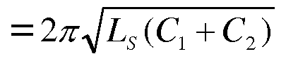 ) 的一半结束, 流过谐振电感器 Ls的谐振电 流 is变为零, 于是, 第一整流二极管 D1切换为关断而不需要反向恢复。
当主开关管 Tl关断、 箝位开关管 T2开通(反激工作状态)时, 以同样的 方式实现第二整流二极管 D2的零电流开关。
) 的一半结束, 流过谐振电感器 Ls的谐振电 流 is变为零, 于是, 第一整流二极管 D1切换为关断而不需要反向恢复。
当主开关管 Tl关断、 箝位开关管 T2开通(反激工作状态)时, 以同样的 方式实现第二整流二极管 D2的零电流开关。
对于第一、 第二整流二极管 D1与 D2, 反激工作状态下第一整流晶体 管的反向电压 VRD1和正激工作状态下第二整流二极管的反向电压 VRD2分 别为:
VRD1=V0- ( Vsi+Vs2 ) =V0-Vr ( - ) ( 1 )
VRD2=V0- ( Vsi+VS2 ) =V0-Vin ( - ) ( 2 ) 其中, Vo为输出电压, 81与 VS2分别为正激绕组与反激绕组的电压, Vin 为输入电压, Vr 为箝位电容器上的电压, NP为变压器原方绕组的匝数, NS1与 NS2分别为正激绕组和反激绕组的匝数, 由于 Lm远远大于 Lr, 故 Lr可省略。
由公式(1 ) 、 (2 )可以看出, 如果 NS1=NS2, 则 VRD1=VRD2=V0。 与 此形成对比的是, 在图 1所示的反激式 DC -DC变换器拓朴中, 副方整流 二极管上的反向电压为 V0+Vin/n,其中, n为原方绕组与副方绕组匝数比。 对比可见, 在根据本发明的实施例的正反激 DC -DC 变换器拓朴中, 可选 用较低电压额定值的整流二极管。
可以想到, 利用副方整流二极管反向电压与正、 反激绕组匝数之间的 这种关系, 能够对变换器拓朴作出进一步的优化。在更为有利的实施例中, 可以根据副方输出电压的不同, 使变换器在正激工作状态和反激工作状态 下传输不同大小的能量,例如,如果使大部分能量在正激工作状态下传输, 由于流过第一整流二极管 D1的电流将会比流过第二整流二极管 D2的电流 大得多, 通过将副方绕组匝数设置为 NS2>NS1, 可以将第一整流二极管 D1 的反向电压进一步降低为小于 V0,从而借助将具有较小反向耐压(正向通 态压降也随之较小)的二极管用作第一整流二极管 D1 来进一步降低副方 损耗。 换言之, 通过调整副方正激绕组匝数和反激绕组匝数的大小关系, 可以使副方整流二极管的反向电压不同, 从而最优地选取具有最佳适合的
反向耐压性能的整流管, 把效率作得最优。
本领域技术人员可以容易地基于图 3所示的拓朴结构来设计和选择高 频变压器、 电感器、 电容器和半导体开关器件的参数, 设计和选择控制模 块、 驱动模块、 采样电路及其他外围电路, 制作出正反激 DC -DC变换器。 例如, DC -DC变换器的控制模块可使用 PWM调制专用芯片,其内部集成 了振荡器、 误差比较器、 PWM调制器、 驱动电路和 /或保护电路, 仅用集 成芯片外加少量的电路即可构成控制简单、 稳定性好的开关电源。 由于控 制芯片和外围元器件的设计属于本领域技术人员的公知常识, 此处省略对 其的详细介绍。
本领域技术人员可以明了,采用根据本发明的实施例的正反激 DC -DC 变换器拓朴, 通过副方侧谐振电路, 实现了副方整流二极管 Dl、 D2的零 电流开关, 副方侧损耗和电磁干 4½射均得到减小; 同时, 由于正反激拓 朴在原方侧具有较低的峰值电流,可使原方侧半导体器件的导通损耗减小。 综合以上因素, 根据本发明的实施例的正反激 DC -DC 变换器拓朴的效率 高于反激式拓朴的效率, 并可满足无风扇应用场合的需要, 同时, 由于副 方整流二极管的反向电压较低, 可选用额定值较低的器件, 以降低成本。 两种拓朴在输入电压 Vin=360V DC ,输出功率 P0=480W,输出电压 V0=40、 60、 80、 96、 120、 160、 240、 320V DC 的测试条件下的效率对比在图 6 中示出, 由图 6可以看出, 效率提高最大可达 3%。 此外, 可以注意到, 输出电流越低(输出电压越高) , 根据本发明的实施例的正反激 DC -DC 变换器拓朴的效率越高, 因此, 本发明所公开的拓朴在高输出电压的应用 场合下尤其适用。
表 1示出了在 P0=480W的情况下选择副方二极管的实例。 如表 1所示, 可随着输出电压的变化而选择合适的副方侧整流二极管, 其中, 具有 200、 400、 600、 800V反向重复峰值电压(VRRM )参数的二极管对于图 1所示 反激式拓朴被选择, 具有 100、 200、 400反向重复峰值电压(VRRM )参数 的二极管对于图 3所示根据本发明的拓朴被选择, 以满足不同的最大反向 电压( Max.Rev.Vol. )要求。
为方便比较起见, 图 2所示现有技术中的正反激变换器拓朴的情况也 在图 6和表 1中示出,在这种拓朴中, 由于大部分电流流经 D1、 D4而 D2、 D3、 D5中的电流较小, 故 D2、 D3、 D5的损 目比可忽略, 仅在表 1中 列出 Dl、 D4的选择。 由图 6和表 1可以看出, 根据本发明的实施例的拓 朴与图 2所示拓朴相比, 成本接近、 但效率更高。
图 7示出了图 2和 3所示的两种正反激变换器拓朴在负载变化情况下 的效率对比(测试^ 输入电压 Vin=360V DC ,输出电压 V0=275V DC ), 可以看出, 从轻负载到重负载的变化范围内, 根据本发明的实施例的拓朴 保持了高的效率, 并且, 效率随着输出功率的增大而增大, 甚至高达 96% 以上。
表 1 随着 V0变化的副方二极管选择 ( P0=480W )

第一变型
图 8示出了应用于根据本发明的实施例的正反激 DC -DC变换器拓朴 的谐振电路的第一变型, 其采用与图 3所示谐振电路不同的形式, 实现副 方整流二极管的零电流开关。 如图 8所示, 谐振电路包含第一电感器 LS1、 第二电感器 LS2、 第一电容器 (^以及第二电容器 C2。 第一电感器 LS1与第 一电容器 d串联连接在第一输出端子和正激与反激绕组的异名端之间,第 二电感器 LS2与第二电容器 C2串联连接在第二输出端子和正激与反激绕组 的异名端之间。
第二变型
图 9示出了应用于根据本发明的实施例的正反激 DC -DC变换器拓朴 的谐振电路的第二变型, 其采用与图 3、 8所示谐振电路不同的形式, 实现 副方整流二极管的零电流开关。如图 9所示,谐振电路包含第一电感器 LS1、 第二电感器 LS2、 第一电容器 (^以及第二电容器 C2。 第一电感器 LS1连接 在第一整流开关管 D1与第一输出端子之间,第二电感器 LS2连接在第二整 流开关管 D2与第二输出端子之间, 第一电容器 与第二电容器 C2串联 连接在第一输出端子与第二输出端子之间 , 正激绕组与反激绕组的异名端 连接到第一电容器 与第二电容器 C2的中间节点。
在不脱离本发明的一般发明构思的情况下, 本领域技术人员可以想到 使用其他的 LC谐振电路实现副方整流二极管的零电流开关并将之与图 4 示出的示例性拓朴结构以及其他类似的拓朴结构自由组合, 例如, 使用与 图 3、 8、 9中的谐振电路具有相同等效电路的谐振电路。
尽管通过对其具体实施例的描述和图示介绍了本发明, 本发明的范围不限 制于这些具体细节。 本领域技术人员将会明了, 在不脱离本发明所提出的 一般发明构思的精神和范围的情况下, 可作出对这些细节的多种修改、 替 代和变型。 因此,本发明在其更为宽广的实施形态上不限于这些具体细节、 示例性结构和连接方式, 其范围由所附权利要求及其等价内容给出。
Claims
1. 一种正反激 DC -DC变换器拓朴, 其特征在于包含变压器、 主开关 管、 箝位电路、 第一与第二整流开关管、 LC 谐振电路以及输出电容器, 其中 , 变压器的原方绕组与主开关管串联连接在第一输入端子与第二输入 端子之间, 由串联连接的箝位电容器和箝位开关管构成的箝位电路与原方 绕组或主开关管并联连接, 变压器的副方绕组包含正激绕组和反激绕组, 令电流流入原方绕组的一端为原方绕组的同名端, 变压器副方的连接方式 为: 正激绕组的同名端经由第一整流开关管连接到第一输出端子, 反激绕 组的同名端经由第二整流开关管连接到第二输出端子, LC 谐振电路连接 到第一输出端子、 第二输出端子以及正激绕组与反激绕组的异名端以使第 一与第二整流开关管实现零电流开关, 输出电容器连接在第一输出端子与 第二输出端子之间。
2. 根据权利要求 1的正反激 DC -DC变换器拓朴, 其中, LC谐振电 路包含第一电容器、 第二电容器以及谐振电感器, 第一电容器与第二电容 器串联连接在第一输出端子与第二输出端子之间, 谐振电感器的一端连接 到正激绕组与反激绕组的异名端, 另一端连接到第一电容器与第二电容器 的中间节点。
3. 根据权利要求 1的正反激 DC -DC变换器拓朴, 其中, LC谐振电 路包含第一电感器、 第二电感器、 第一电容器以及第二电容器, 第一电感 器与第一电容器串联连接在第一输出端子和正激与反激绕组的异名端之 间, 第二电感器与第二电容器串联连接在第二输出端子和正激与反激绕组 的异名端之间。
4. 根据权利要求 1的正反激 DC -DC变换器拓朴, 其中, LC谐振电 路包含第一电感器、 第二电感器、 第一电容器以及第二电容器, 第一电感 器连接在第一整流开关管与第一输出端子之间, 第二电感器连接在第二整 流开关管与第二输出端子之间, 第一电容器与第二电容器串联连接在第一 输出端子与第二输出端子之间, 正激绕组与反激绕组的异名端连接到第一 电容器与第二电容器的中间节点。
5.根据权利要求 1-4中任意一项的正反激 DC -DC变换器拓朴,其中, 正激绕组和反激绕组的匝数比为 1: 1。
6.根据权利要求 1-4中任意一项的正反激 DC -DC变换器拓朴,其中, 在变换器在正激工作状态下的 DC -DC 功率传输大于在反激工作状态下的 DC -DC功率传输的条件下,使反激绕组的匝数多于正激绕组的匝数,在变 换器在反激工作状态下的 DC -DC 功率传输大于在正激工作状态下的 DC -DC功率传输的条件下, 使正激绕组的匝数多于反激绕组的匝数。
7.根据权利要求 1-4中任意一项的正反激 DC -DC变换器拓朴,其中, 整流开关管为二极管或为 MOSFETo
8.根据权利要求 1-4中任意一项的正反激 DC -DC变换器拓朴,其中, 变压器具有漏感。
9.根据权利要求 1-4中任意一项的正反激 DC -DC变换器拓朴,其中, 当进入主开关管开通且箝位开关管关断的正激工作状态时, 第一整流 开关管开通, 第二整流开关管关断, LC 谐振电路开始谐振, 在主开关管 切换为关断之前, 使得流过 LC谐振电路的谐振电流变为零, 以实现第一 整流开关管的零电流开关; 且其中
当进入主开关管关断且箝位开关管开通的反激工作状态时, 第一整流 开关管关断, 第二整流开关管开通, LC 谐振电路开始谐振, 在主开关管 切换为开通之前, 使得流过 LC谐振电路的谐振电流变为零, 以实现第二 整流开关管的零电流开关。
10.根据权利要求 8的正反激 DC -DC变换器拓朴,其中,在主开关管 关断时, 箝位电容器与变压器漏感产生谐振, 使得主开关管和箝位开关管 获得零电压开关, 通过谐振将变压器漏感的能量传递到副方, 避免变压器 漏感的能量损耗以及瞬间造成的主开关管上的电压尖峰。
Priority Applications (2)
| Application Number | Priority Date | Filing Date | Title |
|---|---|---|---|
| US14/233,675 US9419531B2 (en) | 2011-07-21 | 2012-07-23 | Forward-flyback DC-DC converter using resonant LC output circuit |
| EP12814566.1A EP2736157A4 (en) | 2011-07-21 | 2012-07-23 | TOP-RETURN DC-DC CONVERTER WITH HIGH EFFICIENCY AND LOW COST |
Applications Claiming Priority (2)
| Application Number | Priority Date | Filing Date | Title |
|---|---|---|---|
| CN201110205472.7A CN102891608B (zh) | 2011-07-21 | 2011-07-21 | 一种高效率低成本正反激dc-dc变换器拓扑 |
| CN201110205472.7 | 2011-07-21 |
Publications (1)
| Publication Number | Publication Date |
|---|---|
| WO2013010510A1 true WO2013010510A1 (zh) | 2013-01-24 |
Family
ID=47535009
Family Applications (1)
| Application Number | Title | Priority Date | Filing Date |
|---|---|---|---|
| PCT/CN2012/079030 Ceased WO2013010510A1 (zh) | 2011-07-21 | 2012-07-23 | 一种高效率低成本正反激dc-dc变换器拓扑 |
Country Status (4)
| Country | Link |
|---|---|
| US (1) | US9419531B2 (zh) |
| EP (1) | EP2736157A4 (zh) |
| CN (1) | CN102891608B (zh) |
| WO (1) | WO2013010510A1 (zh) |
Cited By (4)
| Publication number | Priority date | Publication date | Assignee | Title |
|---|---|---|---|---|
| CN111740613A (zh) * | 2020-07-09 | 2020-10-02 | 朝阳微电子科技股份有限公司 | 一种应用于dcdc变换的谐振正激有源钳位电路 |
| CN112821483A (zh) * | 2020-12-31 | 2021-05-18 | 维沃移动通信有限公司 | 充电器 |
| CN114070090A (zh) * | 2021-11-19 | 2022-02-18 | 北京创四方电子集团股份有限公司 | 一种串联型有源钳位的反激变换器电路 |
| CN117277822A (zh) * | 2023-11-20 | 2023-12-22 | 威胜能源技术股份有限公司 | 一种用于换电柜的多路输出电路及其自动均流控制方法 |
Families Citing this family (55)
| Publication number | Priority date | Publication date | Assignee | Title |
|---|---|---|---|---|
| JP5857489B2 (ja) * | 2011-07-15 | 2016-02-10 | サンケン電気株式会社 | 共振コンバータ |
| EP2693619A2 (en) * | 2012-08-03 | 2014-02-05 | Samsung Electro-Mechanics Co., Ltd | Single stage forward-flyback converter and power supply apparatus |
| CN103346677B (zh) * | 2013-06-05 | 2016-05-25 | 江苏高博智融科技有限公司 | 一种动态占空比补偿装置 |
| US9077254B2 (en) * | 2013-07-12 | 2015-07-07 | Solantro Semiconductor Corp. | Switching mode power supply using pulse mode active clamping |
| CN103618458A (zh) * | 2013-12-20 | 2014-03-05 | 南京工业大学 | 三绕组变压器副边输出串联正反激倍压整流变换器 |
| CN103812359B (zh) * | 2014-01-16 | 2016-08-17 | 深圳市保益新能电气有限公司 | 一种交流-直流变换电路及其控制方法 |
| TWI513164B (zh) * | 2014-04-18 | 2015-12-11 | Lite On Technology Corp | 返馳式主動箝位電源轉換器 |
| JP6424533B2 (ja) * | 2014-09-17 | 2018-11-21 | 株式会社リコー | 電圧共振型インバータ装置及びその制御方法と表面改質装置 |
| CN104507198B (zh) * | 2014-11-12 | 2017-11-07 | 瑞芙贝(武汉)光电科技发展有限公司 | 有源箝位正、反激推挽集成灯控制器 |
| CN105337514A (zh) * | 2014-12-22 | 2016-02-17 | 韩腊生 | 半波交流电源高频开关隔离变换合成功率因数校正 |
| RU2581600C1 (ru) * | 2014-12-23 | 2016-04-20 | Акционерное общество "Научно-производственное объединение автоматики имени академика Н.А. Семихатова" | Двухтактный обратноходовой преобразователь постоянного напряжения в постоянное |
| KR20160125676A (ko) * | 2015-04-22 | 2016-11-01 | 주식회사 동아일렉콤 | 자려식 액티브 클램프를 적용한 플라이백 컨버터 |
| US9774270B2 (en) | 2015-06-15 | 2017-09-26 | Apple Inc. | Systems and methods of operation for power converters having series-parallel mode active clamps |
| US20180205311A1 (en) | 2017-01-17 | 2018-07-19 | Apple Inc. | Control of Series-Parallel Mode (SPM) Clamped Flyback Converter |
| US9716437B2 (en) * | 2015-12-18 | 2017-07-25 | Champion Microelectronic Corporation | Power converter for a switching power supply and manner of operation thereof |
| RU2635364C2 (ru) * | 2016-02-25 | 2017-11-13 | Закрытое акционерное общество "Связь инжиниринг" | Двухтактный dc/dc-преобразователь |
| CN109075694B (zh) * | 2016-05-04 | 2020-10-23 | 驱动封闭合资股份公司 | 在电感负载中生成高脉冲电压的方法 |
| CN106100352B (zh) * | 2016-08-05 | 2019-02-05 | 广州金升阳科技有限公司 | 反激控制电路及控制方法 |
| CN106385179A (zh) * | 2016-10-19 | 2017-02-08 | 南京博兰得电子科技有限公司 | 副边谐振式隔离电源变换装置 |
| CN106533240B (zh) * | 2016-12-28 | 2023-04-07 | 江苏宏微科技股份有限公司 | 零电压零电流开关的三电平Buck变换器及其控制方法 |
| CN106550512B (zh) * | 2017-01-13 | 2018-06-26 | 重庆理工大学 | 一种谐振软开关单级式led驱动电路 |
| US20190036459A1 (en) * | 2017-04-28 | 2019-01-31 | Astec International Limited | Flyback power converters including adaptive clamp circuits for adjusting resonant frequencies |
| TWI650926B (zh) * | 2017-10-16 | 2019-02-11 | 立錡科技股份有限公司 | 具主動箝位之返馳式電源轉換電路及其中之轉換控制電路與控制方法 |
| EP3484040A1 (en) * | 2017-11-09 | 2019-05-15 | CE+T Power Luxembourg SA | Inverter with ac forward bridge and improved dc/dc topology |
| CN107732916B (zh) * | 2017-11-21 | 2020-11-24 | 国家电网公司 | 并联型谐波电能提取装置 |
| US10418912B2 (en) * | 2017-12-21 | 2019-09-17 | Silanna Asia Pte Ltd | Power converter with active clamp |
| CN108988632B (zh) * | 2018-07-04 | 2019-10-29 | 广州金升阳科技有限公司 | 一种开关变换器 |
| CN109378973A (zh) * | 2018-11-07 | 2019-02-22 | 合肥司耀电子科技有限公司 | 一种用于低压储能装置大功率升压的推挽正激变换器 |
| CN109787479A (zh) * | 2019-03-13 | 2019-05-21 | 南昌航空大学 | 一种包含双谐振腔的双向变换电路以及变换器 |
| US11114945B2 (en) | 2019-08-22 | 2021-09-07 | Cypress Semiconductor Corporation | Secondary-controlled active clamp implementation for improved efficiency |
| CN110690824A (zh) * | 2019-08-23 | 2020-01-14 | 华为数字技术(苏州)有限公司 | 一种反激变换器及电子设备 |
| CN110649816A (zh) * | 2019-09-20 | 2020-01-03 | 广州金升阳科技有限公司 | 一种降压型开关变换器 |
| JP7219688B2 (ja) * | 2019-09-26 | 2023-02-08 | 株式会社日立製作所 | 電力変換装置とその制御方法 |
| CN110912409B (zh) * | 2019-11-07 | 2020-12-18 | 广州金升阳科技有限公司 | 一种正反激式开关电源电路 |
| CN110855151B (zh) * | 2019-11-26 | 2020-12-18 | 广州金升阳科技有限公司 | 一种正反激式开关电源电路及其控制方法 |
| CN111030460A (zh) * | 2019-12-02 | 2020-04-17 | 广州金升阳科技有限公司 | 高压输出变换器 |
| US11996719B2 (en) * | 2020-03-27 | 2024-05-28 | Milwaukee Electric Tool Corporation | Modular storage unit with charger for power tool battery packs |
| CN112234834A (zh) * | 2020-09-30 | 2021-01-15 | 鑫金微半导体(深圳)有限公司 | 一种新型提高反激电源输出功率和提高效率的方法 |
| CN114301295A (zh) * | 2020-10-07 | 2022-04-08 | 浙江杭可仪器有限公司 | 一种直流集成电源及其设计方法 |
| US11342854B1 (en) * | 2020-12-18 | 2022-05-24 | The United States Of America As Represented By The Secretary Of The Army | Voltage step-up converter circuits for low input voltages |
| CN113054853A (zh) * | 2021-03-28 | 2021-06-29 | 青岛大学 | 有源箝位推挽升降压式直流变换器 |
| US11728740B2 (en) * | 2021-06-14 | 2023-08-15 | Apple Inc. | Flyback converters with improved magnetic configurations |
| US11695345B2 (en) | 2021-06-14 | 2023-07-04 | Apple Inc. | Power converter magnetic configurations |
| CN113410994B (zh) * | 2021-06-24 | 2023-03-14 | 广州金升阳科技有限公司 | 一种有源钳位反激变换器及其控制方法 |
| CN115566904A (zh) | 2021-07-02 | 2023-01-03 | 台达电子工业股份有限公司 | 功率转换电路 |
| US12081131B2 (en) | 2021-08-02 | 2024-09-03 | Transient Plasma Systems, Inc. | Power converter comprising series resonant converter(s) having a full-bridge series resonant topology and methods of operating same |
| US20230207188A1 (en) * | 2021-12-27 | 2023-06-29 | Indian Institute Of Technology Kanpur | Differential transformer based voltage converter and method thereof |
| KR20230141552A (ko) * | 2022-03-31 | 2023-10-10 | 박찬웅 | 영 볼트 스위칭을 수행하는 플라이백 방식 전원장치와 그것의 동작 방법 |
| CN114759803B (zh) * | 2022-06-15 | 2022-09-13 | 湖北工业大学 | 一种不对称多模式变频宽输出llc变换器及设计方法 |
| CN116683770A (zh) * | 2023-04-20 | 2023-09-01 | 北京交通大学 | 可实现高升压比的单端双激隔离dc-dc电路 |
| CN116599353A (zh) * | 2023-05-11 | 2023-08-15 | 杭州电子科技大学 | 一种变结构的同步反激变换器及控制方法 |
| KR102631874B1 (ko) * | 2023-05-30 | 2024-02-01 | (주)아이엠피 | 전관 방송용 클래스-d 앰프에 전력을 공급하기 위한 스위칭 모드 전력 공급기 |
| TWI880804B (zh) * | 2024-02-20 | 2025-04-11 | 立錡科技股份有限公司 | 電源轉換電路及其控制方法 |
| KR102815243B1 (ko) * | 2024-04-16 | 2025-06-02 | 인하대학교 산학협력단 | 낮은 트랜스포머 오프셋 전류를 갖는 더블 엔디드 액티브 클램프 포워드 컨버터 |
| CN118523511A (zh) * | 2024-05-14 | 2024-08-20 | Oppo广东移动通信有限公司 | 充电电路、电源电路、电子设备及供电系统 |
Citations (5)
| Publication number | Priority date | Publication date | Assignee | Title |
|---|---|---|---|---|
| CN1132297C (zh) * | 2000-01-24 | 2003-12-24 | 浙江大学 | 一种零电流软开关直流/直流变换电路 |
| CN2764050Y (zh) * | 2004-12-02 | 2006-03-08 | 成都迈科高技术开发有限责任公司 | 基于谐振开关技术的单端反激直流-直流变换器 |
| US7061778B2 (en) * | 2004-06-07 | 2006-06-13 | Power Integrations, Inc. | Method and apparatus for extending the operating range of a flyforward converter |
| CN2917083Y (zh) * | 2005-11-04 | 2007-06-27 | 周春香 | 正激-反激合并式dc/dc隔离变换器 |
| CN100514817C (zh) * | 2007-04-29 | 2009-07-15 | 北京新雷能有限责任公司 | 一种零电压开关有源箝位正反激变换器 |
Family Cites Families (19)
| Publication number | Priority date | Publication date | Assignee | Title |
|---|---|---|---|---|
| US4092509A (en) * | 1975-05-12 | 1978-05-30 | Mitchell Mclaren P | Induction heating appliance circuit that produces relatively high frequency signals directly from a relatively low frequency AC power input |
| NL7702638A (nl) * | 1977-03-11 | 1978-09-13 | Philips Nv | Geschakelde voedingsspanningsschakeling. |
| US4209826A (en) * | 1978-06-14 | 1980-06-24 | Coilcraft, Inc. | Regulated switching mode power supply |
| US5973939A (en) * | 1996-08-29 | 1999-10-26 | Trw Inc. | Double forward converter with soft-PWM switching |
| JP3556120B2 (ja) * | 1999-04-21 | 2004-08-18 | 株式会社三社電機製作所 | 共振形スイッチング電源装置 |
| US6317341B1 (en) * | 2000-11-09 | 2001-11-13 | Simon Fraidlin | Switching circuit, method of operation thereof and single stage power factor corrector employing the same |
| EP1257048B1 (de) * | 2001-05-09 | 2017-10-04 | Philips Lighting Holding B.V. | Regelvorrichtung für einen resonanten Konverter |
| EP1303032A3 (de) * | 2001-09-04 | 2005-02-09 | Philips Intellectual Property & Standards GmbH | Regelvorrichtung für einen resonanten Konverter |
| US6646895B1 (en) * | 2001-10-25 | 2003-11-11 | Tyco Electronics Power Systems, Inc. | Bias supply circuit and a switching power supply employing the same |
| TWI222778B (en) * | 2003-07-30 | 2004-10-21 | Delta Electronics Inc | Lose-less voltage-clamping circuit |
| US7009849B2 (en) * | 2003-10-28 | 2006-03-07 | Tyco Electronics Power Systems, Inc. | Buck converter with multiple outputs and method of operation thereof |
| TWI313102B (en) * | 2005-02-21 | 2009-08-01 | Delta Electronics Inc | Llc series resonant converter and the driving method of the synchronous rectifier power switches thereof |
| JP4626338B2 (ja) * | 2005-02-25 | 2011-02-09 | サンケン電気株式会社 | 直流変換装置 |
| TWI346449B (en) * | 2007-08-16 | 2011-08-01 | Ind Tech Res Inst | Power amplifier circuit for multi-frequencies and multi-modes and method for operating the same |
| TWI338996B (en) * | 2007-10-16 | 2011-03-11 | Delta Electronics Inc | Resonant converter system having synchronous rectifier control circuit and controlling method thereof |
| TWI354443B (en) * | 2008-04-01 | 2011-12-11 | Glacialtech Inc | Half-bridge llc resonant converter with self-drive |
| US8000112B2 (en) * | 2008-04-11 | 2011-08-16 | Flextronics Ap, Llc | Active snubber for transition mode power converter |
| TWI358188B (en) * | 2008-09-17 | 2012-02-11 | Delta Electronics Inc | Forward-flyback converter with active-clamp circui |
| CN101692595B (zh) * | 2009-09-21 | 2011-11-09 | 山特电子(深圳)有限公司 | 一种有源箝位正-反激变换器 |
-
2011
- 2011-07-21 CN CN201110205472.7A patent/CN102891608B/zh not_active Expired - Fee Related
-
2012
- 2012-07-23 US US14/233,675 patent/US9419531B2/en active Active
- 2012-07-23 EP EP12814566.1A patent/EP2736157A4/en not_active Withdrawn
- 2012-07-23 WO PCT/CN2012/079030 patent/WO2013010510A1/zh not_active Ceased
Patent Citations (5)
| Publication number | Priority date | Publication date | Assignee | Title |
|---|---|---|---|---|
| CN1132297C (zh) * | 2000-01-24 | 2003-12-24 | 浙江大学 | 一种零电流软开关直流/直流变换电路 |
| US7061778B2 (en) * | 2004-06-07 | 2006-06-13 | Power Integrations, Inc. | Method and apparatus for extending the operating range of a flyforward converter |
| CN2764050Y (zh) * | 2004-12-02 | 2006-03-08 | 成都迈科高技术开发有限责任公司 | 基于谐振开关技术的单端反激直流-直流变换器 |
| CN2917083Y (zh) * | 2005-11-04 | 2007-06-27 | 周春香 | 正激-反激合并式dc/dc隔离变换器 |
| CN100514817C (zh) * | 2007-04-29 | 2009-07-15 | 北京新雷能有限责任公司 | 一种零电压开关有源箝位正反激变换器 |
Non-Patent Citations (1)
| Title |
|---|
| See also references of EP2736157A4 * |
Cited By (7)
| Publication number | Priority date | Publication date | Assignee | Title |
|---|---|---|---|---|
| CN111740613A (zh) * | 2020-07-09 | 2020-10-02 | 朝阳微电子科技股份有限公司 | 一种应用于dcdc变换的谐振正激有源钳位电路 |
| CN112821483A (zh) * | 2020-12-31 | 2021-05-18 | 维沃移动通信有限公司 | 充电器 |
| CN112821483B (zh) * | 2020-12-31 | 2024-01-05 | 维沃移动通信有限公司 | 充电器 |
| CN114070090A (zh) * | 2021-11-19 | 2022-02-18 | 北京创四方电子集团股份有限公司 | 一种串联型有源钳位的反激变换器电路 |
| CN114070090B (zh) * | 2021-11-19 | 2023-08-22 | 北京创四方电子集团股份有限公司 | 一种串联型有源钳位的反激变换器电路 |
| CN117277822A (zh) * | 2023-11-20 | 2023-12-22 | 威胜能源技术股份有限公司 | 一种用于换电柜的多路输出电路及其自动均流控制方法 |
| CN117277822B (zh) * | 2023-11-20 | 2024-01-30 | 威胜能源技术股份有限公司 | 一种用于换电柜的多路输出电路及其自动均流控制方法 |
Also Published As
| Publication number | Publication date |
|---|---|
| CN102891608A (zh) | 2013-01-23 |
| EP2736157A4 (en) | 2015-10-21 |
| EP2736157A1 (en) | 2014-05-28 |
| CN102891608B (zh) | 2016-03-30 |
| US20140226367A1 (en) | 2014-08-14 |
| US9419531B2 (en) | 2016-08-16 |
Similar Documents
| Publication | Publication Date | Title |
|---|---|---|
| CN102891608B (zh) | 一种高效率低成本正反激dc-dc变换器拓扑 | |
| CN108028605B (zh) | 具有保持操作的转换器 | |
| US9660536B2 (en) | Switching power supply device performs power transmission by using resonance phenomenon | |
| US9106141B2 (en) | Switching power supply device | |
| CN101615840B (zh) | 具有窄操作频段的谐振电路及共振式电源转换器 | |
| CN103546038B (zh) | 一种抑制副边电压振荡的软开关全桥直流变换器 | |
| WO2019036201A1 (en) | BIDIRECTIONAL LEVEL 1 ELECTRIC VEHICLE CHARGER WITH SINGLE-PHASE SINGLE FLOOR | |
| CN100448148C (zh) | 二极管加电流互感器箝位的零电压开关全桥直流变换器 | |
| WO2024051181A1 (zh) | 一种双向谐振型直流变换器的控制方法及控制电路 | |
| CN109302078B (zh) | 基于同步整流模式的dc-dc开关电源 | |
| CN108988645A (zh) | 一种基于llc谐振的新颖软开关双向dc-dc变换器拓扑 | |
| CN106787776A (zh) | 一种混合控制的llc谐振变换器 | |
| CN101355307A (zh) | 一种零电压零电流全桥dc-dc变换器 | |
| CN101860216A (zh) | 加耦合电感的倍流整流方式全桥直流变换器 | |
| CN111682780A (zh) | 提高原边反馈有源箝位反激变换器轻载效率的控制方法 | |
| CN103595258A (zh) | 一种升压型软开关谐振变换器及其定频控制方法 | |
| TW202247587A (zh) | 適用於寬範圍輸出電壓的變換器及其控制方法 | |
| CN100431250C (zh) | 副边箝位的隔离型直流变换器 | |
| TW556395B (en) | Resonant reset dual-switch forward DC-to-DC converter | |
| CN107005171A (zh) | 电力变换单元 | |
| CN205544948U (zh) | 一种混合控制的llc谐振变换器 | |
| CN112838766A (zh) | 一种高降压比三电平llc谐振变换器及其控制方法 | |
| CN110299849A (zh) | 一种移相控制的交错并联双管正激变换器 | |
| KR101270326B1 (ko) | 센터-탭 커패시터를 가진 두 스위치 플라이백 컨버터 | |
| CN108347174B (zh) | 一种Boost全桥隔离型变换器及其复合有源箝位电路 |
Legal Events
| Date | Code | Title | Description |
|---|---|---|---|
| 121 | Ep: the epo has been informed by wipo that ep was designated in this application |
Ref document number: 12814566 Country of ref document: EP Kind code of ref document: A1 |
|
| NENP | Non-entry into the national phase |
Ref country code: DE |
|
| WWE | Wipo information: entry into national phase |
Ref document number: 2012814566 Country of ref document: EP |
|
| WWE | Wipo information: entry into national phase |
Ref document number: 14233675 Country of ref document: US |