WO2013015009A1 - 分光器 - Google Patents
分光器 Download PDFInfo
- Publication number
- WO2013015009A1 WO2013015009A1 PCT/JP2012/063661 JP2012063661W WO2013015009A1 WO 2013015009 A1 WO2013015009 A1 WO 2013015009A1 JP 2012063661 W JP2012063661 W JP 2012063661W WO 2013015009 A1 WO2013015009 A1 WO 2013015009A1
- Authority
- WO
- WIPO (PCT)
- Prior art keywords
- light
- unit
- spectroscopic
- light detection
- detection unit
- Prior art date
- Legal status (The legal status is an assumption and is not a legal conclusion. Google has not performed a legal analysis and makes no representation as to the accuracy of the status listed.)
- Ceased
Links
Images


Classifications
-
- G—PHYSICS
- G01—MEASURING; TESTING
- G01J—MEASUREMENT OF INTENSITY, VELOCITY, SPECTRAL CONTENT, POLARISATION, PHASE OR PULSE CHARACTERISTICS OF INFRARED, VISIBLE OR ULTRAVIOLET LIGHT; COLORIMETRY; RADIATION PYROMETRY
- G01J3/00—Spectrometry; Spectrophotometry; Monochromators; Measuring colours
- G01J3/02—Details
- G01J3/0256—Compact construction
-
- G—PHYSICS
- G01—MEASURING; TESTING
- G01J—MEASUREMENT OF INTENSITY, VELOCITY, SPECTRAL CONTENT, POLARISATION, PHASE OR PULSE CHARACTERISTICS OF INFRARED, VISIBLE OR ULTRAVIOLET LIGHT; COLORIMETRY; RADIATION PYROMETRY
- G01J3/00—Spectrometry; Spectrophotometry; Monochromators; Measuring colours
- G01J3/02—Details
- G01J3/0202—Mechanical elements; Supports for optical elements
-
- G—PHYSICS
- G01—MEASURING; TESTING
- G01J—MEASUREMENT OF INTENSITY, VELOCITY, SPECTRAL CONTENT, POLARISATION, PHASE OR PULSE CHARACTERISTICS OF INFRARED, VISIBLE OR ULTRAVIOLET LIGHT; COLORIMETRY; RADIATION PYROMETRY
- G01J3/00—Spectrometry; Spectrophotometry; Monochromators; Measuring colours
- G01J3/02—Details
- G01J3/0256—Compact construction
- G01J3/0259—Monolithic
-
- G—PHYSICS
- G01—MEASURING; TESTING
- G01J—MEASUREMENT OF INTENSITY, VELOCITY, SPECTRAL CONTENT, POLARISATION, PHASE OR PULSE CHARACTERISTICS OF INFRARED, VISIBLE OR ULTRAVIOLET LIGHT; COLORIMETRY; RADIATION PYROMETRY
- G01J3/00—Spectrometry; Spectrophotometry; Monochromators; Measuring colours
- G01J3/02—Details
- G01J3/0262—Constructional arrangements for removing stray light
-
- G—PHYSICS
- G01—MEASURING; TESTING
- G01J—MEASUREMENT OF INTENSITY, VELOCITY, SPECTRAL CONTENT, POLARISATION, PHASE OR PULSE CHARACTERISTICS OF INFRARED, VISIBLE OR ULTRAVIOLET LIGHT; COLORIMETRY; RADIATION PYROMETRY
- G01J3/00—Spectrometry; Spectrophotometry; Monochromators; Measuring colours
- G01J3/02—Details
- G01J3/0264—Electrical interface; User interface
-
- G—PHYSICS
- G01—MEASURING; TESTING
- G01J—MEASUREMENT OF INTENSITY, VELOCITY, SPECTRAL CONTENT, POLARISATION, PHASE OR PULSE CHARACTERISTICS OF INFRARED, VISIBLE OR ULTRAVIOLET LIGHT; COLORIMETRY; RADIATION PYROMETRY
- G01J3/00—Spectrometry; Spectrophotometry; Monochromators; Measuring colours
- G01J3/02—Details
- G01J3/0291—Housings; Spectrometer accessories; Spatial arrangement of elements, e.g. folded path arrangements
-
- G—PHYSICS
- G01—MEASURING; TESTING
- G01J—MEASUREMENT OF INTENSITY, VELOCITY, SPECTRAL CONTENT, POLARISATION, PHASE OR PULSE CHARACTERISTICS OF INFRARED, VISIBLE OR ULTRAVIOLET LIGHT; COLORIMETRY; RADIATION PYROMETRY
- G01J3/00—Spectrometry; Spectrophotometry; Monochromators; Measuring colours
- G01J3/12—Generating the spectrum; Monochromators
- G01J3/18—Generating the spectrum; Monochromators using diffraction elements, e.g. grating
Definitions
- the spectroscopic module of the spectroscope further includes a light-shielding member disposed between the light detection unit and the spectroscopic unit.
- the light-shielding member splits and reflects light that has passed through the light-passing portion and the spectroscopic portion.
- An opening that allows the transmitted light to pass therethrough may be provided. According to this configuration, it is possible to suppress stray light from entering the light detection unit.
- Each lead pin 8 extends in a direction in which the light incident portion 6 and the stem 4 face each other (hereinafter referred to as “longitudinal direction”), and is a hermetic material made of low melting point glass having light shielding properties and electrical insulation properties.
- the tick seal member 9 is fixed to the through hole 4 a of the stem 4. Note that a plurality of through holes 4 a are arranged on each of a pair of side edge portions facing each other in the rectangular plate-like stem 4.
- the molding layer 33 has a concave curved surface 33c that faces a bottom surface 32b that is a predetermined inner surface of the concave portion 32.
- the curved surface 33 c is a curved surface that is recessed toward the center of the bottom surface 32 b of the recess 32, and passes through the midpoint of each side of the opening 32 a of the recess 32 to reach each riding-up portion 33 b from the main body portion 33 a.
- a grating pattern corresponding to a blazed grating having a sawtooth cross section, a binary grating having a rectangular cross section, a holographic grating having a sinusoidal cross section, or the like is formed in a predetermined region on the main body 33a of the curved surface 33c. In this grating pattern, a plurality of grating grooves extending in the back direction are arranged in parallel in the horizontal direction.
- the through hole 4 a of the stem 4, the through hole 13 c of the spacer 13, the hole 36 of the substrate 31, the through hole 11 c of the spacer 11 and the hole 29 of the substrate 21 that are opposed in the vertical direction are continuous.
- the inner diameters of the through hole 13 c, the hole 36, the through hole 11 c and the hole 29 are sufficiently larger than the outer diameter of the lead pin 8.
- a lead pin 8 that penetrates the stem 4 and extends into the package 2 is inserted into each of the continuous through hole 13 c, hole 36, through hole 11 c, and hole 29. As a result, the lead pin 8 is inserted and fitted into the hole 29 provided in the light detection unit 20 in the package 2.
- the light L ⁇ b> 1 enters the package 2 from the light incident portion 6 of the package 2 and passes through the slit 22 of the light detection unit 20.
- the light L1 that has passed through the slit 22 reaches the spectroscopic unit 35 of the spectroscopic unit 30, is split by the spectroscopic unit 35, and is reflected by the light detection unit 26 of the photodetection unit 20.
- the light L ⁇ b> 2 that is split and reflected by the spectroscopic unit 35 passes through the light passage opening 23 of the light detection unit 20, reaches the light detection unit 26 of the light detection element 24, and is detected by the light detection element 24.
- the stem 4 is prepared, and the lead pin 8 is fixed to each through hole 4 a of the stem 4.
- a spectroscopic module 3A is prepared.
- the slit 22 of the light detection unit 20 and the spectroscopic unit 35 of the spectroscopic unit 30, and further, the spectroscopic unit 35 of the spectroscopic unit 30 and the light detection unit 26 of the photodetection unit 20 replace the spacer 11.
- positioning is performed in the three directions of the vertical direction, the horizontal direction, and the back direction.
- the lead pin 8 is inserted into the through hole 13 c of the spacer 13, and the other end portion 13 b of the spacer 13 is fixed to the stem 4. Subsequently, the lead pin 8 is inserted into the hole 36, the through hole 11 c and the hole 29 that are continuous in the spectroscopic module 3 ⁇ / b> A, and the one end 13 a of the spacer 13 is fixed to the substrate 31. Subsequently, as shown in FIG. 7B, the cap 5 is disposed on the stem 4 so as to cover the spectral module 3A, and the stepped portion of the stem 4 and the flange 5a of the cap 5 are joined by welding. Thus, the spectroscope 1A is manufactured.
- the spectroscope 1 ⁇ / b> A is configured such that the slit 22 provided in the package 2 is positioned with respect to the light incident portion 6 provided in the package 2.
- the electrical connection between the light detection unit 26 and the outside of the package 2 and the positioning of the slit 22 with respect to the light incident unit 6 are realized simultaneously by the lead pins 8.
- the light shielding member 14 is formed with a plurality of through holes 14 b so as to be continuous with the hole 36 of the substrate 31, the through hole 11 c of the spacer 11 and the hole 29 of the substrate 21 which are opposed in the vertical direction. That is, each lead pin 8 is also inserted through the corresponding through hole 14 b of the light shielding member 14.
- the spectroscope 1 ⁇ / b> B configured as described above can suppress stray light from entering the light detection unit 26 provided in the light detection unit 20 by the light shielding member 14.
- the spectroscope 1B can reduce stray light due to multiple reflection in the spectroscope 1B.
- the light shielding member 14 may be disposed at a position other than the position in contact with the back surface 21b of the substrate 21 of the light detection unit 20 as long as it is between the light detection unit 20 and the spectroscopic unit 30.
- the light passage opening that allows the light L1 to pass therethrough and the light passage that allows the light L2 to pass therethrough may be formed separately in the light shielding member 14.
- the end portions 8a of the lead pins 8 are arranged and fitted in the corresponding concave portions 41.
- the slit 22 provided in the light detection unit 20 is not only in the horizontal direction and the back direction but also in the vertical direction with respect to the light incident part 6 provided in the package 2 via the plurality of lead pins 8.
- the light detection unit 60 has a rectangular plate-like substrate 61 made of BK7, Pyrex (registered trademark), light-transmitting glass such as quartz, plastic, or the like.
- a plurality of wirings 66 are formed on the surface 61 a of the substrate 61 opposite to the spectroscopic unit 70.
- Each wiring 66 has a light reflection preventing layer on the surface 61 a side of the substrate 61.
- the light reflection preventing layer is formed of a single layer film such as Al, Au, or CrO or a laminated film such as Cr—CrO, Cr—Pt—Au, Ti—Pt—Au, Ti—Ni—Au, or Cr—Au.
- a light shielding layer 62 is formed on the surface 61 a of the substrate 61 so as to expose only the pad portion of the wiring 66 and cover other portions of the wiring 66.
- a slit (light passage portion) 63 extending in a predetermined direction and a rectangular light passage opening 64 are formed.
- the light shielding layer 62 is patterned into a predetermined shape, and is a black resin, a colored resin (silicone, epoxy, acrylic, urethane, polyimide, composite resin, etc.) containing filler (carbon, oxide, etc.), Cr, Co, etc. These are integrally formed of a metal, a metal oxide, a laminated film thereof, a porous ceramic, a metal, a metal oxide, or the like.
- a plurality of grating grooves extending in the back direction are arranged in parallel in the horizontal direction.
- the spectroscopic unit 72 splits the light L1 that has passed through the slit 63 of the light detection unit 60 and reflects the split light L2 to the light detection unit 26 of the light detection unit 60.
- the diffraction layer 73 is formed by photocuring a replica optical resin such as a photocurable epoxy resin, an acrylic resin, or an organic / inorganic hybrid resin.
- the reflection layer 74 is formed by evaporating Al, Au, or the like on the outer surface of the diffraction layer 73.
- a plurality of holes (fitting portions) 65 penetrating from the spectroscopic unit 70 side to the opposite side are formed in the substrate 61 of the light detection unit 60.
- a plurality of holes 65 are arranged in each of a pair of side edge portions facing each other in the rectangular plate-like substrate 61.
- Each hole 65 includes a quadrangular frustum-shaped portion 65a that widens toward the spectroscopic unit 70, and a columnar portion 65b connected to the top of the portion 65a.
- the light L ⁇ b> 2 that is split and reflected by the spectroscopic unit 72 passes through the light transmitting member 71 and the substrate 61, and further passes through the light passage opening 64 of the light detection unit 60, so that the light detection unit 26 of the light detection element 24. , And is detected by the light detection element 24.
- a spectroscopic module 3D is prepared.
- the slit 63 of the photodetection unit 60 and the spectroscopic unit 72 of the spectroscopic unit 70, and further, the spectroscopic unit 72 of the spectroscopic unit 70 and the photodetection unit 26 of the photodetection unit 60 include spacers and the like. It is directly positioned in the three directions of the vertical direction, the horizontal direction, and the back direction without being interposed. Subsequently, the lead pin 8 is inserted into the hole 65 of the substrate 61 of the light detection unit 60, and the one end 81 a of the spacer 81 is fixed to the substrate 61.
- the cap 5 is disposed on the stem 4 so as to cover the spectral module 3D, and the step portion of the stem 4 and the flange 5a of the cap 5 are joined by welding.
- the spectroscope 1D is manufactured.
- the spectroscope 1 ⁇ / b> D As described above, in the spectrometer 1 ⁇ / b> D, the plurality of lead pins 8 that penetrate the stem 4 facing the light incident portion 6 in the package 2 are inserted and fitted into the holes 65 provided in the light detection unit 60. . Accordingly, the slit 63 provided in the light detection unit 60 is positioned in the lateral direction and the back direction with respect to the light incident portion 6 provided in the package 2 via the plurality of lead pins 8.
- the spectroscope 1D since the plurality of lead pins 8 face each other with a predetermined distance in the horizontal direction in which the slit 63 and the light detection unit 26 are arranged, the positioning accuracy in the horizontal direction is improved. Therefore, the spectroscope 1 ⁇ / b> D is configured such that the slit 63 provided in the package 2 is positioned with respect to the light incident portion 6 provided in the package 2.
- the lead pin 8 is inserted into the continuous through hole 81c and hole 65 in the spacer 81 and the light detection unit 60, the lead pin 8 is held by the spacer 81 and the light detection unit 60. Wire bonding to the end portion 8a of 8 can be easily and reliably performed.
- the fitting portion provided in the light detection unit of the spectroscopic module and into which the lead pin is fitted is not limited to a hole penetrating from the spectroscopic unit side to the opposite side or a recess opening to the spectroscopic unit side.
- the fitting portion may be a plurality of convex portions formed on the back surface of the substrate of the light detection unit so as to restrict the movement of the end portion of the lead pin in the lateral direction and the back direction.
- the fitting part is a hole penetrating from the spectroscopic unit side to the opposite side or a concave part opening to the spectroscopic unit side, it is easy to position the light passage part relative to the light incident part in the lateral direction and the back direction. And reliably realized.
- An insulating film 91 is formed on the surface 21a of the substrate 21, the inner surface 29e of the first portion 29c, the back surface 21b of the substrate 21, and the inner surface 29f of the second portion 29d.
- Metal wiring 92 is formed on the insulating film 91 formed on the back surface 21b of the substrate 21 and the inner surface 29f of the second portion 29d.
- the lead pin 8 is inserted into the hole 29, and the lead pin 8 is electrically connected to the metal wiring 92 by the conductive resin 93 filled in the second portion 29d.
- an insulating film 91 is formed on the surface 21a of the substrate 21, the inner surface 29e of the first portion 29c, the back surface 21b of the substrate 21, and the inner surface 29f of the second portion 29d.
- the insulating film 95 is made of an insulating material such as silicon oxide (SiO 2 ) or silicon nitride (SiN).
- metal wiring 92 is formed by mask vapor deposition on the insulating film 91 formed on the back surface 21b of the substrate 21 and the inner surface 29f of the second portion 29d.
- the hole 29 is formed.
- the lead pin 8 is inserted into the hole 29.
- the second portion 29 d is filled with the conductive resin 93, and the lead pin 8 is electrically connected to the metal wiring 92.
- the edge portion 21c of the opening portion is compared with the method of forming the fitting portion by penetrating alkali etching from one side. , 21d becomes gentle, so that the substrate 21 can be prevented from being damaged.
- the above-described method of forming the fitting portion by etching from both surfaces of the substrate 21 may be used for forming the light passage portion (slit) 22. According to this, damage to the substrate 21 can be suppressed.
- the light passing portions 22 and 63 that allow the light L1 incident from the light incident portion 6 to pass therethrough are provided in the light detection units 20 and 60 such as slits formed in the semiconductor substrate 25 of the light detection element 24. That's fine.
- the materials and shapes of the constituent members of the spectrometers 1A, 1B, 1C, and 1D are not limited to the materials and shapes described above, and various materials and shapes can be applied. Further, when the lead pin 8 has sufficient strength, the spectroscopic modules 3A, 3B, 3C may be supported by the lead pin 8 without using the spacer 11.
- the light passing portions 22 and 63 provided in the package 2 can be positioned with respect to the light incident portion 6 provided in the package 2.
Landscapes
- Physics & Mathematics (AREA)
- Spectroscopy & Molecular Physics (AREA)
- General Physics & Mathematics (AREA)
- Engineering & Computer Science (AREA)
- Human Computer Interaction (AREA)
- Spectrometry And Color Measurement (AREA)
Abstract
分光器1Aは、光入射部6が設けられたパッケージ2と、パッケージ2のうち光入射部6と対向する支持部4を貫通する複数のリードピン8と、パッケージ2内において支持部4上に支持された分光モジュール3Aと、を備える。分光モジュール3Aは、光入射部6から入射した光L1を通過させる光通過部22が設けられた光検出ユニット20と、光検出ユニット20に対して支持部4側に配置されるように光検出ユニット20に固定され、光通過部22を通過した光L1を分光すると共に光検出部26に反射する分光部35を有する分光ユニット30と、を有する。リードピン8は、光検出ユニット20に設けられた嵌め部29に嵌められ、光検出部26と電気的に接続されている。
Description
本発明は、光を分光して検出する分光器に関する。
従来の分光器として、光入射部、分光部及び光検出部がパッケージの壁部に固定されたものが知られている(例えば、特許文献1参照)。このような分光器では、光入射部から入射した光が、分光部において分光されると共に反射されて、光検出部によって検出される。
近年、様々な測定システムや分光測定装置に適用される分光器の小型化が進められている。分光器の小型化に際しては、パッケージに設けられた光入射部に対する各構成部の高精度な位置決めが必要となる。特に、光入射部に対してスリット等の光通過部がパッケージ内に設けられる場合には、光入射部に対する光通過部の位置決めが重要となる。
そこで、本発明は、パッケージに設けられた光入射部に対して、パッケージ内に設けられた光通過部が位置決めされた分光器を提供することを目的とする。
本発明の一観点の分光器は、光入射部が設けられたパッケージと、パッケージのうち光入射部と対向する支持部を貫通する複数のリードピンと、パッケージ内において支持部上に支持された分光モジュールと、を備える。分光モジュールは、光入射部から入射した光を通過させる光通過部が設けられた光検出ユニットと、光検出ユニットに対して支持部側に配置されるように光検出ユニットに固定され、光通過部を通過した光を分光すると共に光検出ユニットの光検出部に反射する分光部を有する分光ユニットと、を有する。リードピンは、光検出ユニットに設けられた嵌め部に嵌められ、光検出部と電気的に接続されている。
この分光器では、パッケージのうち光入射部と対向する支持部を貫通する複数のリードピンが、光検出ユニットに設けられた嵌め部に嵌められている。これにより、光検出ユニットに設けられた光通過部が、複数のリードピンを介して、パッケージに設けられた光入射部に対し、少なくとも光入射部と支持部とが対向する方向に垂直な方向において位置決めされる。よって、この分光器は、パッケージに設けられた光入射部に対して、パッケージ内に設けられた光通過部が位置決めされたものとなる。
なお、「光検出ユニットに固定された分光ユニット」とは、分光ユニットが光検出ユニットに直接的に固定されている場合だけでなく、分光ユニットが光検出ユニットに間接的に固定されている場合も含む意味である(ただし、分光ユニットと光検出ユニットとの接続において支持部は介されない)。
上記分光器の分光モジュールは、光検出ユニットと分光ユニットとの間に配置されたスペーサを更に有し、分光ユニットは、スペーサを介して光検出ユニットに固定されていてもよい。この構成によれば、光通過部と分光部とが、更には、分光部と光検出部とが、スペーサを介して、光入射部と支持部とが対向する方向において位置決めされる。
上記分光器の分光モジュールは、光検出ユニットと分光ユニットとの間に配置された遮光部材を更に有し、遮光部材には、光通過部を通過した光、及び分光部において分光されると共に反射された光を通過させる開口部が設けられていてもよい。この構成によれば、光検出部に迷光が入射することを抑制することができる。
上記分光器の分光ユニットは、光検出ユニットと接触した状態で光検出ユニットに固定されていてもよい。この構成によれば、光通過部と分光部とが、更には、分光部と光検出部とが、直接的に、光入射部と支持部とが対向する方向において位置決めされる。
上記分光器の嵌め部は、分光ユニット側からその反対側に貫通する孔であり、リードピンは、パッケージ内において嵌め部に挿通されていてもよい。或いは、上記分光器の嵌め部は、分光ユニット側に開口する凹部であり、リードピンの端部は、パッケージ内において嵌め部に配置されていてもよい。これらの構成によれば、少なくとも光入射部と支持部とが対向する方向に垂直な方向において、光入射部に対する光通過部の位置決めが容易に且つ確実に実現される。
本発明によれば、パッケージに設けられた光入射部に対して、パッケージ内に設けられた光通過部が位置決めされた分光器を提供することができる。
以下、本発明の好適な実施形態について、図面を参照して詳細に説明する。なお、各図において同一又は相当部分には同一符号を付し、重複する説明を省略する。
<第1実施形態>
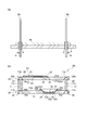
図1及び図2に示されるように、分光器1Aは、いわゆるCANパッケージの構成を有するパッケージ2と、パッケージ2内に収容された分光モジュール3Aと、を備えている。分光器1Aは、パッケージ2外からパッケージ2内に入射した光L1を分光して検出するものである。なお、パッケージ2の一辺の長さは、例えば10~20mm程度である。
図1及び図2に示されるように、分光器1Aは、いわゆるCANパッケージの構成を有するパッケージ2と、パッケージ2内に収容された分光モジュール3Aと、を備えている。分光器1Aは、パッケージ2外からパッケージ2内に入射した光L1を分光して検出するものである。なお、パッケージ2の一辺の長さは、例えば10~20mm程度である。
パッケージ2は、周縁部に段差部が設けられた矩形板状のステム(支持部)4と、直方体箱状のキャップ5と、を有している。ステム4及びキャップ5は金属からなる。キャップ5は、開口端から外側に向かって突出するフランジ5aを有し、このフランジ5aとステム4の段差部とが溶接により接合され、開口部分が塞がれている。これにより、パッケージ2の気密化が図られ、分光器1Aの信頼性の向上が図られている。
キャップ5においてステム4と対向する壁部5bには、光入射部6が設けられている。つまり、ステム4は、光入射部6と対向している。光入射部6は、キャップ5の壁部5bに形成された断面円形状の光通過孔5cが、円形板状の窓部材7によって内側から気密に覆われることで、構成されている。なお、窓部材7は、例えば、石英、硼珪酸ガラス(BK7)、パイレックス(登録商標)ガラス、コバール等、光L1を透過させる材料からなる。また、窓部材7には、必要に応じて、AR(Anti Reflection)コートや、不要な波長をカットする波長カットフィルタ(フィルタレジストや誘電体多層膜等)、バンドパスフィルタが施されてもよい。
ステム4には、銅等の導電性材料からなる複数のリードピン8が貫通している。各リードピン8は、光入射部6とステム4とが対向する方向(以下、「縦方向」という)に延在しており、遮光性と電気的絶縁性とを有する低融点ガラスからなるハーメティックシール部材9を介して、ステム4の貫通孔4aに固定されている。なお、貫通孔4aは、矩形板状のステム4において対向する一対の側縁部のそれぞれに、複数ずつ配置されている。
分光モジュール3Aは、パッケージ2内においてステム4上に支持されている。分光モジュール3Aは、光検出ユニット20と、光検出ユニット20に対してステム4側に配置された分光ユニット30と、光検出ユニット20と分光ユニット30との間に配置された複数のスペーサ11と、を有している。分光ユニット30は、スペーサ11を介して光検出ユニット20に固定されている。
図3及び図4に示されるように、光検出ユニット20は、樹脂やセラミック、シリコン、ガラス等からなる矩形板状の基板21を有している。基板21には、所定の方向に延在するスリット(光通過部)22が形成されている。スリット22は、パッケージ2に設けられた光入射部6と縦方向において対向しており、光入射部6から入射した光L1を通過させる。なお、スリット22における分光ユニット30側の端部は、スリット22の延在方向(以下、「奥方向」という)、及び、奥方向に垂直且つ縦方向に垂直な方向(以下、「横方向」という)の両方向において、分光ユニット30側に向かって末広がりとなっている。
基板21における分光ユニット30と反対側の表面21aには、光検出素子24が固定されている。光検出素子24は、シリコン等の半導体材料からなる半導体基板25と、半導体基板25における基板21側の面に形成された光検出部26と、を有している。光検出部26は、フォトダイオードアレイ、C-MOSイメージセンサ、CCDイメージセンサ等である。光検出素子24は、基板21に形成された断面矩形状の光通過開口23に光検出部26が対向するように、基板21の表面21aに固定されている。光通過開口23は、横方向においてスリット22と並ぶように形成されている。なお、光通過開口23における分光ユニット30側の端部は、奥方向及び横方向の両方向において、分光ユニット30側に向かって末広がりとなっている。
基板21の表面21aには、光検出部26に対する入出力信号等を伝送するための複数の配線27が設けられている。各配線27の一端部は、Auや半田等のバンプ28を介して光検出部26と電気的に接続されている。各配線27の他端部は、パッド部27aとなっている。各パッド部27aは、対応するリードピン8の端部8aと、ワイヤ12によってワイヤボンディングされている。これにより、リードピン8は、光検出部26と電気的に接続される。
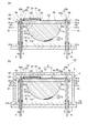
図3及び図5に示されるように、分光ユニット30は、シリコン、プラスチック、セラミック又はガラス等からなる矩形板状の基板31を有している。基板31における光検出ユニット20側の表面31aには、奥方向及び横方向の両方向において、光検出ユニット20側に向かって末広がりとなる正四角錐台状の凹部32が形成されている。
基板31には、成形層33が、凹部32を覆うように配置されている。成形層33は、光硬化性のエポキシ樹脂、アクリル樹脂、フッ素系樹脂、シリコーン又は有機・無機ハイブリッド樹脂等のレプリカ用光学樹脂を光硬化させることによって形成されている。成形層33は、凹部32の深さ方向(すなわち、光検出ユニット20側)から見た場合に円形状となっており、成形層33の外縁33dは、凹部32の開口32aの各頂点を通っている。
成形層33は、一体的に形成された本体部33a及び乗上げ部33bを有している。本体部33aは、凹部32の深さ方向から見た場合に凹部32内に位置しており、凹部32の底面32b及び側面32cの全体を覆っている。乗上げ部33bは、本体部33aと繋がった状態で基板31の表面31aに位置しており、凹部32の開口32aの各辺の外側に設けられている。つまり、乗上げ部33bは、凹部32を挟んで対向し且つ凹部32を包囲するように複数設けられている。
成形層33は、凹部32の所定の内面である底面32bと対向する凹状の曲面33cを有している。曲面33cは、凹部32の底面32bの中心に向かって凹んだ曲面であり、凹部32の開口32aの各辺の中点を通って、本体部33aから各乗上げ部33bに至っている。曲面33cにおける本体部33a上の所定の領域には、鋸歯状断面のブレーズドグレーティング、矩形状断面のバイナリグレーティング、又は正弦波状断面のホログラィックグレーティング等に対応するグレーティングパターンが形成されている。このグレーティングパターンは、奥方向に延在するグレーティング溝が横方向に複数並設されたものである。
成形層33の曲面33c上には、AlやAu等の蒸着膜である反射膜34が形成されている。反射膜34は、曲面33cにおける本体部33a上の所定の領域ではグレーティングパターンに対応するように形成されており、この部分が、反射型グレーティングである分光部35となっている。分光ユニット30が有する分光部35は、光検出ユニット20のスリット22を通過した光L1を分光すると共に、分光した光L2を光検出ユニット20の光検出部26に反射する。
図3に示されるように、光検出ユニット20の基板21には、分光ユニット30側からその反対側に貫通する孔(嵌め部)29が複数形成されている。孔29は、矩形板状の基板21において対向する一対の側縁部のそれぞれに、複数ずつ配置されている。各孔29は、分光ユニット30側に向かって末広がりとなる四角錐台状の部分29aと、その部分29aの頂部に接続された円柱状の部分29bと、を含んでいる。
また、分光ユニット30の基板31には、光検出ユニット20側からその反対側に貫通する断面円形状の孔36が複数形成されている。孔36は、矩形板状の基板31において対向する一対の側縁部のそれぞれに、複数ずつ配置されている。各孔36は、光検出ユニット20の反対側に向かって末広がりとなる四角錐台状の部分36aと、その部分36aの頂部に接続された円柱状の部分36bと、を含んでいる。
スペーサ11は、金属やプラスチック、セラミック、シリコン、ガラス等により円柱状に形成されており、縦方向において対向する基板21の孔29と基板31の孔36との間にそれぞれ配置されている。スペーサ11の一端部11aは、対応する孔29の部分29a内に配置され、接着等により基板21に固定されている。スペーサ11の他端部11bは、対応する孔36の部分36bを覆うように基板31の表面31aに配置され、接着等により基板31に固定されている。各スペーサ11には、縦方向に貫通孔11cが形成されており、各貫通孔11cは、対応する孔29及び孔36と一続きとなっている。
図1に示されるように、分光モジュール3Aは、複数のスペーサ13を介して、ステム4におけるパッケージ2内の表面4b上に配置されている。スペーサ13は、金属等により円柱状に形成されており、縦方向において対向するステム4の貫通孔4aと基板31の孔36との間にそれぞれ配置されている。スペーサ13の一端部13aは、対応する孔36の部分36a内に配置され、接着等により基板31に固定されている。スペーサ13の他端部13bは、対応する貫通孔4aを覆うようにステム4の表面4bに配置され、接着等によりステム4に固定されている。各スペーサ13には、縦方向に貫通孔13cが形成されており、各貫通孔13cは、対応する孔36及び貫通孔4aと一続きとなっている。
つまり、縦方向において対向するステム4の貫通孔4a、スペーサ13の貫通孔13c、基板31の孔36、スペーサ11の貫通孔11c及び基板21の孔29は、一続きとなっている。これらの貫通孔13c、孔36、貫通孔11c及び孔29の内径は、リードピン8の外径よりも十分に大きくなっている。そして、一続きとなっている貫通孔13c、孔36、貫通孔11c及び孔29のそれぞれには、ステム4を貫通してパッケージ2内に延在するリードピン8が挿通されている。これにより、リードピン8は、パッケージ2内において、光検出ユニット20に設けられた孔29に挿通され、嵌められる。孔29の内面(ここでは部分29bの内面)に対するリードピン8の側面の接触状態には、リードピン8の側面の一部のみが孔29の内面に接触する状態や、リードピン8の側面の全部が孔29の内面に接触する状態だけでなく、リードピン8の側面の全部が孔29の内面に接触しない状態も含まれる。
以上のように構成された分光器1Aにおいては、光L1は、パッケージ2の光入射部6からパッケージ2内に入射し、光検出ユニット20のスリット22を通過する。スリット22を通過した光L1は、分光ユニット30の分光部35に到達し、分光部35において分光されると共に光検出ユニット20の光検出部26に反射される。分光部35において分光されると共に反射された光L2は、光検出ユニット20の光通過開口23を通過して光検出素子24の光検出部26に到達し、光検出素子24によって検出される。
次に、分光器1Aの製造方法について説明する。まず、図6(a)に示されるように、ステム4を準備し、ステム4の各貫通孔4aにリードピン8を固定する。その一方で、図6(b)に示されるように、分光モジュール3Aを準備する。分光モジュール3Aにおいては、光検出ユニット20のスリット22と分光ユニット30の分光部35とが、更には、分光ユニット30の分光部35と光検出ユニット20の光検出部26とが、スペーサ11を介して、縦方向、横方向及び奥方向の三方向において位置決めされている。
続いて、図7(a)に示されるように、スペーサ13の貫通孔13cにリードピン8を挿通させ、スペーサ13の他端部13bをステム4に固定する。続いて、分光モジュール3Aにおいて一続きとなっている孔36、貫通孔11c及び孔29にリードピン8を挿通させ、スペーサ13の一端部13aを基板31に固定する。続いて、図7(b)に示されるように、分光モジュール3Aを覆うようにキャップ5をステム4に配置し、ステム4の段差部とキャップ5のフランジ5aとを溶接により接合する。以上により、分光器1Aが製造される。
以上説明したように、分光器1Aでは、パッケージ2において光入射部6と対向するステム4を貫通する複数のリードピン8が、光検出ユニット20に設けられた孔29に挿通され、嵌められている。これにより、光検出ユニット20に設けられたスリット22が、複数のリードピン8を介して、パッケージ2に設けられた光入射部6に対し、横方向及び奥方向において位置決めされる。特に、分光器1Aでは、スリット22と光検出部26とが並ぶ横方向において複数のリードピン8が所定の距離をとって対向しているため、横方向における位置決めの精度が向上される。よって、分光器1Aは、パッケージ2に設けられた光入射部6に対して、パッケージ2内に設けられたスリット22が位置決めされたものとなる。このように、分光器1Aでは、リードピン8によって、光検出部26とパッケージ2の外部との間の電気的な接続と、光入射部6に対するスリット22の位置決めとが同時に実現される。
また、スペーサ13及び分光モジュール3Aにおいて一続きとなっている貫通孔13c、孔36、貫通孔11c及び孔29にリードピン8が挿通されているため、スペーサ13、分光ユニット30、スペーサ11及び光検出ユニット20によってリードピン8が保持された状態となり、リードピン8の端部8aへのワイヤボンディングを容易に且つ確実に行うことができる。
次に、第1実施形態の分光器の変形例について説明する。図8に示されるように、分光器1Bは、分光モジュール3Bが遮光部材14を有している点で、上述した分光器1Aと主に相違している。
遮光部材14は、遮光性の材料により矩形板状に形成されており、光検出ユニット20の基板21の裏面21bに接触した状態で固定されている。遮光部材14には、基板21のスリット22及び光通過開口23に対向するように光通過開口(開口部)14aが形成されている。つまり、光通過開口14aは、スリット22を通過した光L1、及び分光部35において分光されると共に反射された光L2を通過させる。
また、遮光部材14には、縦方向において対向する基板31の孔36、スペーサ11の貫通孔11c及び基板21の孔29と一続きとなるように、貫通孔14bが複数形成されている。つまり、各リードピン8は、対応する遮光部材14の貫通孔14bにも挿通させられている。
以上のように構成された分光器1Bは、遮光部材14によって、光検出ユニット20に設けられた光検出部26に迷光が入射することを抑制することができる。また、分光器1Bは、分光器1B内の多重反射による迷光を低減することができる。
なお、遮光部材14は、光検出ユニット20と分光ユニット30との間であれば、光検出ユニット20の基板21の裏面21bに接触した位置以外の位置に配置されていてもよい。また、スリット22を通過した光L1、及び分光部35において分光されると共に反射された光L2を通過させる開口部であれば、光L1を通過させる光通過開口と、光L2を通過させる光通過開口とが遮光部材14に別々に形成されていてもよい。
次に、第1実施形態の分光器の別の変形例について説明する。図9に示されるように、分光器1Cは、光検出ユニット20に設けられた凹部(嵌め部)41にリードピン8の端部8aが配置されている点で、上述した分光器1Aと主に相違している。
凹部41は、縦方向において基板31の孔36、及びスペーサ11の貫通孔11cと対向するように、基板21の裏面21bに複数形成され、分光ユニット30側に開口している。各リードピン8の端部8aは、スペーサ13及び光検出ユニット20において一続きとなっている貫通孔13c、孔36及び貫通孔11cに各リードピン8が挿通された状態で、対応する凹部41に配置され、嵌められている。
光検出素子24は、光検出部26が分光ユニット30側に向いた状態で、基板21の裏面21bに固定されている。光検出部26と各リードピン8とは、基板21の裏面21bに設けられた配線を介して電気的に接続されている。より具体的には、基板21の裏面21bに設けられた配線は、各凹部41内に至っており、各リードピン8の端部8aと導電性接着剤等により電気的に接続されている。光検出部26と基板21の裏面21bに設けられた配線とはワイヤにて接続されている。
以上のように構成された分光器1Cでは、各リードピン8の端部8aが、対応する凹部41に配置され、嵌められている。これにより、光検出ユニット20に設けられたスリット22が、複数のリードピン8を介して、パッケージ2に設けられた光入射部6に対し、横方向及び奥方向においてだけでなく、縦方向においても位置決めされる。
<第2実施形態>
図10に示されるように、分光器1Dは、分光モジュール3Dにおいて分光ユニット70が光検出ユニット60と接触した状態で光検出ユニット60に固定されている点で、第1実施形態の分光器1Aと主に相違している。
図10に示されるように、分光器1Dは、分光モジュール3Dにおいて分光ユニット70が光検出ユニット60と接触した状態で光検出ユニット60に固定されている点で、第1実施形態の分光器1Aと主に相違している。
分光モジュール3Dにおいて、光検出ユニット60は、BK7、パイレックス(登録商標)、石英等の光透過性ガラス、プラスチック等からなる矩形板状の基板61を有している。基板61における分光ユニット70と反対側の表面61aには、複数の配線66が形成されている。各配線66は、光反射防止層を基板61の表面61a側に有している。光反射防止層は、AlやAu、CrO等の単層膜、或いはCr-CrO、Cr-Pt-Au、Ti-Pt-Au、Ti-Ni-Au、Cr-Au等の積層膜からなる。
基板61の表面61aには、配線66のパッド部のみを露出させ且つ配線66のその他の部分を覆うように遮光層62が形成されている。遮光層62には、所定の方向に延在するスリット(光通過部)63、及び矩形状の光通過開口64が形成されている。遮光層62は、所定の形状にパターニングされて、ブラックレジスト、フィラー(カーボンや酸化物等)を含有する有色の樹脂(シリコーン、エポキシ、アクリル、ウレタン、ポリイミド、複合樹脂等)、CrやCo等の金属又は酸化金属、或いはその積層膜、ポーラス状のセラミックや金属又は酸化金属等によって一体成形される。
スリット63は、パッケージ2に設けられた光入射部6と縦方向(光入射部6とステム4とが対向する方向)において対向しており、光入射部6から入射した光L1を通過させる。光通過開口64は、横方向(奥方向(スリット63の延在方向)に垂直且つ縦方向に垂直な方向)においてスリット63と並ぶように形成されている。
光検出素子24は、基板61の表面61aに固定されている。光検出素子24は、光通過開口64に光検出部26が対向するように、基板61の表面61aに固定されている。各配線66の一端部は、Au等のバンプ28を介して光検出部26と電気的に接続されている。各配線66の他端部は、パッド部66aとなっており、各パッド部66aは、対応するリードピン8の端部8aと、ワイヤ12によってワイヤボンディングされている。
分光ユニット70は、半球状の光透過部材71を有している。光透過部材71は、基板61と同一の材料、光透過性樹脂、光透過性の無機・有機ハイブリッド材料、或いはレプリカ成形用の光透過性低融点ガラス、プラスチック等からなる。光透過部材71における光検出ユニット60側の表面71aは、光検出ユニット60の基板61の裏面61bに光学樹脂材等により固定されている。このように、分光ユニット70は、スペーサ等を介さずに光検出ユニット60と接触した状態で光検出ユニット60に固定されている。
光透過部材71における曲面状の外側表面71bには、分光部72が設けられている。分光部72は、光透過部材71の外側表面71bに形成された回折層73と、回折層73の外側表面に形成された反射層74と、を有する反射型グレーティングである。より具体的には、回折層73には、鋸歯状断面のブレーズドグレーティング、矩形状断面のバイナリグレーティング、又は正弦波状断面のホログラフィックグレーティング等に対応するグレーティングパターンが形成されている。このグレーティングパターンにおいては、奥方向に延在するグレーティング溝が横方向に複数並設されている。分光部72は、光検出ユニット60のスリット63を通過した光L1を分光すると共に、分光した光L2を光検出ユニット60の光検出部26に反射する。
なお、回折層73は、光硬化性のエポキシ樹脂、アクリル樹脂、又は有機・無機ハイブリッド樹脂等のレプリカ用光学樹脂を光硬化させることで形成される。反射層74は、回折層73の外側表面にAlやAu等を蒸着することで形成される。
光検出ユニット60の基板61には、分光ユニット70側からその反対側に貫通する孔(嵌め部)65が複数形成されている。孔65は、矩形板状の基板61において対向する一対の側縁部のそれぞれに、複数ずつ配置されている。各孔65は、分光ユニット70側に向かって末広がりとなる四角錐台状の部分65aと、その部分65aの頂部に接続された円柱状の部分65bと、を含んでいる。
分光モジュール3Dは、複数のスペーサ81を介して、ステム4におけるパッケージ2内の表面4b上に配置されている。スペーサ81は、金属等により円柱状に形成されており、縦方向において対向するステム4の貫通孔4aと基板61の孔65との間にそれぞれ配置されている。スペーサ81の一端部81aは、対応する孔65の部分65a内に配置され、接着等により基板61に固定されている。スペーサ81の他端部81bは、対応する貫通孔4aを覆うようにステム4の表面4bに配置され、接着等によりステム4に固定されている。各スペーサ81には、縦方向に貫通孔81cが形成されており、各貫通孔81cは、対応する孔65及び貫通孔4aと一続きとなっている。
これらの貫通孔81c及び孔65の内径は、リードピン8の外径よりも十分に大きくなっている。そして、一続きとなっている貫通孔81c及び孔65のそれぞれには、ステム4を貫通してパッケージ2内に延在するリードピン8が挿通されている。これにより、リードピン8は、パッケージ2内において、光検出ユニット60に設けられた孔65に挿通され、嵌められる。
以上のように構成された分光器1Dにおいては、光L1は、パッケージ2の光入射部6からパッケージ2内に入射し、光検出ユニット60のスリット63を通過する。スリット63を通過した光L1は、基板61及び光透過部材71を透過して分光ユニット70の分光部72に到達し、分光部72において分光されると共に光検出ユニット60の光検出部26に反射される。分光部72において分光されると共に反射された光L2は、光透過部材71及び基板61を透過し、更に、光検出ユニット60の光通過開口64を通過して光検出素子24の光検出部26に到達し、光検出素子24によって検出される。
次に、分光器1Dの製造方法について説明する。まず、図11(a)に示されるように、ステム4を準備し、ステム4の各貫通孔4aにリードピン8を固定する。続いて、図11(b)に示されるように、スペーサ81の貫通孔81cにリードピン8を挿通させ、スペーサ81の他端部81bをステム4に固定する。
その一方で、図12(a)に示されるように、分光モジュール3Dを準備する。分光モジュール3Dにおいては、光検出ユニット60のスリット63と分光ユニット70の分光部72とが、更には、分光ユニット70の分光部72と光検出ユニット60の光検出部26とが、スペーサ等を介さずに直接的に、縦方向、横方向及び奥方向の三方向において位置決めされている。続いて、光検出ユニット60の基板61の孔65にリードピン8を挿通させ、スペーサ81の一端部81aを基板61に固定する。続いて、図12(b)に示されるように、分光モジュール3Dを覆うようにキャップ5をステム4に配置し、ステム4の段差部とキャップ5のフランジ5aとを溶接により接合する。以上により、分光器1Dが製造される。
以上説明したように、分光器1Dでは、パッケージ2において光入射部6と対向するステム4を貫通する複数のリードピン8が、光検出ユニット60に設けられた孔65に挿通され、嵌められている。これにより、光検出ユニット60に設けられたスリット63が、複数のリードピン8を介して、パッケージ2に設けられた光入射部6に対し、横方向及び奥方向において位置決めされる。特に、分光器1Dでは、スリット63と光検出部26とが並ぶ横方向において複数のリードピン8が所定の距離をとって対向しているため、横方向における位置決めの精度が向上される。よって、分光器1Dは、パッケージ2に設けられた光入射部6に対して、パッケージ2内に設けられたスリット63が位置決めされたものとなる。
また、スペーサ81及び光検出ユニット60において一続きとなっている貫通孔81c及び孔65にリードピン8が挿通されているため、リードピン8がスペーサ81及び光検出ユニット60によって保持された状態となり、リードピン8の端部8aへのワイヤボンディングを容易に且つ確実に行うことができる。
以上、本発明の実施形態について説明したが、本発明は、上記各実施形態に限定されるものではない。例えば、分光モジュールの光検出ユニットに設けられ且つリードピンが嵌められる嵌め部は、分光ユニット側からその反対側に貫通する孔や、分光ユニット側に開口する凹部に限定されない。一例として、嵌め部は、リードピンの端部の横方向及び奥方向への移動を規制するように光検出ユニットの基板の裏面に形成された複数の凸部等であってもよい。ただし、嵌め部が、分光ユニット側からその反対側に貫通する孔や、分光ユニット側に開口する凹部である場合には、横方向及び奥方向において、光入射部に対する光通過部の位置決めが容易に且つ確実に実現される。
嵌め部の構造の他の例について説明する。図13に示されるように、基板21には、裏面21b側から表面21a側に貫通する孔(嵌め部)29が形成されている。孔29は、基板21の表面21aに開口した第1の部分29cと、裏面21bに開口した第2の部分29dとを含んでいる。第1の部分29cは表面21aに向かって末広がりとなる形状(例えば四角錘台状の形状)を有し、第2の部分29dは裏面21bに向かって末広がりとなる形状(例えば四角錘台状の形状)を有する。基板21の表面21a上、第1の部分29cの内面29e上、基板21の裏面21b上及び第2の部分29dの内面29f上には、絶縁膜91が形成されている。基板21の裏面21b上及び第2の部分29dの内面29f上に形成された絶縁膜91上には、メタル配線92が形成されている。孔29にはリードピン8が挿通されており、このリードピン8は、第2の部分29dに充填された導電性樹脂93により、メタル配線92に電気的に接続されている。
次に、上述した孔29を形成する工程について説明する。まず、基板21の表面21a及び裏面21bにエッチングマスクを形成する。次に、フォトワークによりこのエッチングマスクに開口を設ける。このエッチングマスクは酸化シリコン(SiO2)、窒化シリコン(SiN)等からなる。続いて、エッチングマスクを用いて表面21a側からアルカリエッチングを行う。このエッチングにより基板21に第1の部分29cが形成される。続いて、エッチングマスクを用いて裏面21b側からアルカリエッチングを行う。このエッチングにより基板21に第2の部分29dが形成される。続いて、基板21の表面21a上、第1の部分29cの内面29e上、基板21の裏面21b上及び第2の部分29dの内面29f上に絶縁膜91を形成する。この絶縁膜95は、酸化シリコン(SiO2)、窒化シリコン(SiN)等の絶縁性を有する材料からなる。続いて、基板21の裏面21b上及び第2の部分29dの内面29f上に形成された絶縁膜91上にマスク蒸着法によりメタル配線92を形成する。以上により、孔29が形成される。この孔29に対してリードピン8が挿通される。そして、第2の部分29dに導電性樹脂93が充填され、リードピン8がメタル配線92に電気的に接続される。このように、表面21a及び裏面21bの両面から基板21をエッチングして嵌め部を形成する方法によれば、片面からの貫通アルカリエッチングにより嵌め部を形成する方法に比べ、開口部のエッジ部21c,21dの角度が緩やかになるため、基板21の破損を抑制することができる。なお、基板21の両面からエッチングして嵌め部を形成する上記方法は、光通過部(スリット)22の形成に用いてもよい。これによれば、基板21の破損を抑制することができる。
また、光入射部6から入射した光L1を通過させる光通過部22,63は、光検出素子24の半導体基板25に形成されたスリット等、光検出ユニット20,60に設けられたものであればよい。
また、分光器1A,1B,1C,1Dの各構成部材の材料及び形状には、前述した材料及び形状に限らず、様々な材料及び形状を適用することができる。また、リードピン8が十分な強度を有するときには、スペーサ11を用いることなく、分光モジュール3A,3B,3Cがリードピン8により支持されてもよい。
本発明の分光器1A,1B,1C,1Dによれば、パッケージ2に設けられた光入射部6に対して、パッケージ2内に設けられた光通過部22,63を位置決めすることができる。
1A,1B,1C,1D…分光器、2…パッケージ、3A,3B,3D…分光モジュール、4…ステム(支持部)、6…光入射部、8…リードピン、8a…端部、11…スペーサ、14…遮光部材、14a…光通過開口(開口部)、20,60…光検出ユニット、22,63…スリット(光通過部)、26…光検出部、29,65…孔(嵌め部)、30,70…分光ユニット、35,72…分光部、41…凹部(嵌め部)。
Claims (6)
- 光入射部が設けられたパッケージと、
前記パッケージのうち前記光入射部と対向する支持部を貫通する複数のリードピンと、
前記パッケージ内において前記支持部上に支持された分光モジュールと、を備え、
前記分光モジュールは、
前記光入射部から入射した光を通過させる光通過部が設けられた光検出ユニットと、
前記光検出ユニットに対して前記支持部側に配置されるように前記光検出ユニットに固定され、前記光通過部を通過した光を分光すると共に前記光検出ユニットの光検出部に反射する分光部を有する分光ユニットと、を有し、
前記リードピンは、前記光検出ユニットに設けられた嵌め部に嵌められ、前記光検出部と電気的に接続されている分光器。 - 前記分光モジュールは、前記光検出ユニットと前記分光ユニットとの間に配置されたスペーサを更に有し、
前記分光ユニットは、前記スペーサを介して前記光検出ユニットに固定されている請求項1に記載の分光器。 - 前記分光モジュールは、前記光検出ユニットと前記分光ユニットとの間に配置された遮光部材を更に有し、
前記遮光部材には、前記光通過部を通過した光、及び前記分光部において分光されると共に反射された光を通過させる開口部が設けられている請求項2に記載の分光器。 - 前記分光ユニットは、前記光検出ユニットと接触した状態で前記光検出ユニットに固定されている請求項1に記載の分光器。
- 前記嵌め部は、前記分光ユニット側からその反対側に貫通する孔であり、
前記リードピンは、前記パッケージ内において前記嵌め部に挿通されている請求項1~4のいずれか一項に記載の分光器。 - 前記嵌め部は、前記分光ユニット側に開口する凹部であり、
前記リードピンの端部は、前記パッケージ内において前記嵌め部に配置されている請求項1~4のいずれか一項に記載の分光器。
Priority Applications (3)
| Application Number | Priority Date | Filing Date | Title |
|---|---|---|---|
| EP12817232.7A EP2743656B1 (en) | 2011-07-26 | 2012-05-28 | Spectroscope |
| US14/234,674 US9488523B2 (en) | 2011-07-26 | 2012-05-28 | Arrangements for lead pins in a spectroscope |
| CN201280036905.3A CN103718006B (zh) | 2011-07-26 | 2012-05-28 | 分光器 |
Applications Claiming Priority (2)
| Application Number | Priority Date | Filing Date | Title |
|---|---|---|---|
| JP2011163641A JP5767883B2 (ja) | 2011-07-26 | 2011-07-26 | 分光器 |
| JP2011-163641 | 2011-07-26 |
Publications (1)
| Publication Number | Publication Date |
|---|---|
| WO2013015009A1 true WO2013015009A1 (ja) | 2013-01-31 |
Family
ID=47600869
Family Applications (1)
| Application Number | Title | Priority Date | Filing Date |
|---|---|---|---|
| PCT/JP2012/063661 Ceased WO2013015009A1 (ja) | 2011-07-26 | 2012-05-28 | 分光器 |
Country Status (5)
| Country | Link |
|---|---|
| US (1) | US9488523B2 (ja) |
| EP (1) | EP2743656B1 (ja) |
| JP (1) | JP5767883B2 (ja) |
| CN (1) | CN103718006B (ja) |
| WO (1) | WO2013015009A1 (ja) |
Cited By (6)
| Publication number | Priority date | Publication date | Assignee | Title |
|---|---|---|---|---|
| JP2015087318A (ja) * | 2013-10-31 | 2015-05-07 | 浜松ホトニクス株式会社 | 光検出装置 |
| CN105960579A (zh) * | 2014-02-05 | 2016-09-21 | 浜松光子学株式会社 | 分光器及分光器的制造方法 |
| CN105980819A (zh) * | 2014-02-05 | 2016-09-28 | 浜松光子学株式会社 | 分光器 |
| US20170010156A1 (en) * | 2014-02-05 | 2017-01-12 | Hamamatsu Photonics K.K. | Spectroscope |
| TWI655415B (zh) * | 2014-02-05 | 2019-04-01 | 日商濱松赫德尼古斯股份有限公司 | 分光器、及分光器之製造方法 |
| US20200041345A1 (en) * | 2014-02-05 | 2020-02-06 | Hamamatsu Photonics K.K. | Spectroscope and method for producing spectroscope |
Families Citing this family (20)
| Publication number | Priority date | Publication date | Assignee | Title |
|---|---|---|---|---|
| EP2783193A4 (en) | 2011-11-03 | 2015-08-26 | Verifood Ltd | COST-EFFECTIVE SPECTROMETRIC SYSTEM FOR USER-EATING FOOD ANALYSIS |
| GB2529070B (en) | 2013-08-02 | 2017-07-12 | Verifood Ltd | Spectrometer comprising a plurality of isolated optical paths |
| EP3090239A4 (en) | 2014-01-03 | 2018-01-10 | Verifood Ltd. | Spectrometry systems, methods, and applications |
| TWD167889S (zh) | 2014-02-04 | 2015-05-21 | Hamamatsu Photonics Kk | 分光器之部分 |
| USD733599S1 (en) | 2014-02-04 | 2015-07-07 | Hamamatsu Photonics K.K. | Spectrometer |
| EP3209983A4 (en) | 2014-10-23 | 2018-06-27 | Verifood Ltd. | Accessories for handheld spectrometer |
| WO2016125164A2 (en) | 2015-02-05 | 2016-08-11 | Verifood, Ltd. | Spectrometry system applications |
| WO2016125165A2 (en) | 2015-02-05 | 2016-08-11 | Verifood, Ltd. | Spectrometry system with visible aiming beam |
| WO2016162865A1 (en) | 2015-04-07 | 2016-10-13 | Verifood, Ltd. | Detector for spectrometry system |
| US10066990B2 (en) | 2015-07-09 | 2018-09-04 | Verifood, Ltd. | Spatially variable filter systems and methods |
| KR102641685B1 (ko) * | 2015-08-04 | 2024-02-29 | 하마마츠 포토닉스 가부시키가이샤 | 분광기, 및 분광기의 제조 방법 |
| JP6113940B1 (ja) * | 2015-08-04 | 2017-04-12 | 浜松ホトニクス株式会社 | 分光器 |
| US10203246B2 (en) | 2015-11-20 | 2019-02-12 | Verifood, Ltd. | Systems and methods for calibration of a handheld spectrometer |
| US10254215B2 (en) | 2016-04-07 | 2019-04-09 | Verifood, Ltd. | Spectrometry system applications |
| WO2018015951A1 (en) | 2016-07-20 | 2018-01-25 | Verifood, Ltd. | Accessories for handheld spectrometer |
| US10791933B2 (en) | 2016-07-27 | 2020-10-06 | Verifood, Ltd. | Spectrometry systems, methods, and applications |
| KR102806625B1 (ko) * | 2018-07-06 | 2025-05-13 | 하마마츠 포토닉스 가부시키가이샤 | 분광 모듈, 및 분광 모듈의 제조 방법 |
| EP3864384A4 (en) | 2018-10-08 | 2022-06-29 | Verifood Ltd. | Accessories for optical spectrometers |
| DE102019126038A1 (de) * | 2019-09-26 | 2021-04-01 | Robert Bosch Gmbh | Spektrometervorrichtung und Verfahren zur Herstellung einer Spektrometervorrichtung |
| JP2024025075A (ja) * | 2022-08-10 | 2024-02-26 | 浜松ホトニクス株式会社 | 光検出装置及びアパーチャ部 |
Citations (6)
| Publication number | Priority date | Publication date | Assignee | Title |
|---|---|---|---|---|
| JPH11142245A (ja) * | 1997-11-10 | 1999-05-28 | Horiba Ltd | 熱型赤外線検出器 |
| WO2000040935A1 (en) * | 1999-01-08 | 2000-07-13 | Adc Telecommunications, Inc. | Spectrometer |
| JP2000298066A (ja) | 1999-04-01 | 2000-10-24 | Gretag Macbeth Ag | 分光計 |
| JP2004354176A (ja) * | 2003-05-28 | 2004-12-16 | Hamamatsu Photonics Kk | 光検出器及びそれを用いた分光器 |
| JP2007225455A (ja) * | 2006-02-23 | 2007-09-06 | Matsushita Electric Works Ltd | 赤外線検出器 |
| WO2008149939A1 (ja) * | 2007-06-08 | 2008-12-11 | Hamamatsu Photonics K.K. | 分光器 |
Family Cites Families (9)
| Publication number | Priority date | Publication date | Assignee | Title |
|---|---|---|---|---|
| US4699454A (en) * | 1984-03-29 | 1987-10-13 | American Telephone And Telegraph Company, At&T Bell Laboratories | Fiber optic connector |
| JPH11132857A (ja) * | 1997-10-28 | 1999-05-21 | Matsushita Electric Works Ltd | 赤外線検出器 |
| JP2001351266A (ja) * | 2000-04-06 | 2001-12-21 | Fujitsu Ltd | 光ピックアップ及び光記憶装置 |
| JP3912111B2 (ja) | 2002-01-09 | 2007-05-09 | 富士通株式会社 | 波長多重双方向光伝送モジュール |
| JP4836498B2 (ja) | 2005-06-15 | 2011-12-14 | パナソニック株式会社 | 固体撮像装置及びカメラ |
| EP1952108A1 (en) * | 2005-11-22 | 2008-08-06 | Matsushita Electric Works, Ltd | Infrared detector and process for fabricating the same |
| JP5111163B2 (ja) | 2008-03-04 | 2012-12-26 | 浜松ホトニクス株式会社 | 分光器 |
| JP5205239B2 (ja) | 2008-05-15 | 2013-06-05 | 浜松ホトニクス株式会社 | 分光器 |
| JP5767882B2 (ja) * | 2011-07-26 | 2015-08-26 | 浜松ホトニクス株式会社 | 分光器 |
-
2011
- 2011-07-26 JP JP2011163641A patent/JP5767883B2/ja active Active
-
2012
- 2012-05-28 WO PCT/JP2012/063661 patent/WO2013015009A1/ja not_active Ceased
- 2012-05-28 EP EP12817232.7A patent/EP2743656B1/en active Active
- 2012-05-28 US US14/234,674 patent/US9488523B2/en active Active
- 2012-05-28 CN CN201280036905.3A patent/CN103718006B/zh active Active
Patent Citations (6)
| Publication number | Priority date | Publication date | Assignee | Title |
|---|---|---|---|---|
| JPH11142245A (ja) * | 1997-11-10 | 1999-05-28 | Horiba Ltd | 熱型赤外線検出器 |
| WO2000040935A1 (en) * | 1999-01-08 | 2000-07-13 | Adc Telecommunications, Inc. | Spectrometer |
| JP2000298066A (ja) | 1999-04-01 | 2000-10-24 | Gretag Macbeth Ag | 分光計 |
| JP2004354176A (ja) * | 2003-05-28 | 2004-12-16 | Hamamatsu Photonics Kk | 光検出器及びそれを用いた分光器 |
| JP2007225455A (ja) * | 2006-02-23 | 2007-09-06 | Matsushita Electric Works Ltd | 赤外線検出器 |
| WO2008149939A1 (ja) * | 2007-06-08 | 2008-12-11 | Hamamatsu Photonics K.K. | 分光器 |
Non-Patent Citations (1)
| Title |
|---|
| See also references of EP2743656A4 |
Cited By (23)
| Publication number | Priority date | Publication date | Assignee | Title |
|---|---|---|---|---|
| US10066995B2 (en) | 2013-10-31 | 2018-09-04 | Hamamatsu Photonics K.K. | Light-detecting device |
| KR20160079768A (ko) * | 2013-10-31 | 2016-07-06 | 하마마츠 포토닉스 가부시키가이샤 | 광검출 장치 |
| KR102273849B1 (ko) | 2013-10-31 | 2021-07-05 | 하마마츠 포토닉스 가부시키가이샤 | 광검출 장치 |
| US10895501B2 (en) | 2013-10-31 | 2021-01-19 | Hamamatsu Photonics K.K. | Light-detecting device |
| US10775238B2 (en) | 2013-10-31 | 2020-09-15 | Hamamatsu Photonics K.K. | Light-detecting device |
| JP2015087318A (ja) * | 2013-10-31 | 2015-05-07 | 浜松ホトニクス株式会社 | 光検出装置 |
| CN105960579B (zh) * | 2014-02-05 | 2018-02-16 | 浜松光子学株式会社 | 分光器及分光器的制造方法 |
| US20200041345A1 (en) * | 2014-02-05 | 2020-02-06 | Hamamatsu Photonics K.K. | Spectroscope and method for producing spectroscope |
| US9976900B2 (en) | 2014-02-05 | 2018-05-22 | Hamamatsu Photonics K.K. | Spectrometer, and spectrometer production method |
| US10024715B2 (en) | 2014-02-05 | 2018-07-17 | Hamamatsu Photonics K.K. | Spectrometer |
| US9921103B2 (en) | 2014-02-05 | 2018-03-20 | Hamamatsu Photonics K.K. | Spectrometer, and spectrometer production method |
| US10184834B2 (en) * | 2014-02-05 | 2019-01-22 | Hamamatsu Photonics K.K. | Spectroscope |
| TWI655414B (zh) * | 2014-02-05 | 2019-04-01 | 日商濱松赫德尼古斯股份有限公司 | 分光器、及分光器之製造方法 |
| TWI655415B (zh) * | 2014-02-05 | 2019-04-01 | 日商濱松赫德尼古斯股份有限公司 | 分光器、及分光器之製造方法 |
| US20190154504A1 (en) * | 2014-02-05 | 2019-05-23 | Hamamatsu Photonics K.K. | Spectroscope |
| CN105980819B (zh) * | 2014-02-05 | 2018-05-15 | 浜松光子学株式会社 | 分光器 |
| TWI694242B (zh) * | 2014-02-05 | 2020-05-21 | 日商濱松赫德尼古斯股份有限公司 | 分光器 |
| US20170010156A1 (en) * | 2014-02-05 | 2017-01-12 | Hamamatsu Photonics K.K. | Spectroscope |
| US10883877B2 (en) | 2014-02-05 | 2021-01-05 | Hamamatsu Photonics K.K. | Spectroscope |
| CN105980819A (zh) * | 2014-02-05 | 2016-09-28 | 浜松光子学株式会社 | 分光器 |
| US11022493B2 (en) * | 2014-02-05 | 2021-06-01 | Hamamatsu Photonics K.K. | Spectroscope and method for producing spectroscope |
| CN105960579A (zh) * | 2014-02-05 | 2016-09-21 | 浜松光子学株式会社 | 分光器及分光器的制造方法 |
| US11262240B2 (en) | 2014-02-05 | 2022-03-01 | Hamamatsu Photonics K.K. | Spectroscope |
Also Published As
| Publication number | Publication date |
|---|---|
| CN103718006B (zh) | 2017-04-19 |
| CN103718006A (zh) | 2014-04-09 |
| JP5767883B2 (ja) | 2015-08-26 |
| US20140192354A1 (en) | 2014-07-10 |
| EP2743656B1 (en) | 2018-06-20 |
| EP2743656A4 (en) | 2015-03-04 |
| EP2743656A1 (en) | 2014-06-18 |
| US9488523B2 (en) | 2016-11-08 |
| JP2013029327A (ja) | 2013-02-07 |
Similar Documents
| Publication | Publication Date | Title |
|---|---|---|
| JP5767883B2 (ja) | 分光器 | |
| JP5767882B2 (ja) | 分光器 | |
| CN105960579B (zh) | 分光器及分光器的制造方法 | |
| JP6251073B2 (ja) | 分光器、及び分光器の製造方法 | |
| JP6325268B2 (ja) | 分光器、及び分光器の製造方法 | |
| JP6061542B2 (ja) | 分光器 | |
| JP6068039B2 (ja) | 分光器 | |
| JP6104451B1 (ja) | 分光器 | |
| JP6293967B2 (ja) | 分光器、及び分光器の製造方法 | |
| JP6328303B2 (ja) | 分光器 | |
| JP2019144267A (ja) | 分光器 | |
| JP2018105883A (ja) | 分光器 | |
| JP2019002941A (ja) | 分光器 | |
| JP2018138924A (ja) | 分光器 |
Legal Events
| Date | Code | Title | Description |
|---|---|---|---|
| 121 | Ep: the epo has been informed by wipo that ep was designated in this application |
Ref document number: 12817232 Country of ref document: EP Kind code of ref document: A1 |
|
| WWE | Wipo information: entry into national phase |
Ref document number: 14234674 Country of ref document: US |
|
| NENP | Non-entry into the national phase |
Ref country code: DE |
|
| WWE | Wipo information: entry into national phase |
Ref document number: 2012817232 Country of ref document: EP |