WO2013018197A1 - 半導体層の温度測定方法および温度測定装置 - Google Patents
半導体層の温度測定方法および温度測定装置 Download PDFInfo
- Publication number
- WO2013018197A1 WO2013018197A1 PCT/JP2011/067678 JP2011067678W WO2013018197A1 WO 2013018197 A1 WO2013018197 A1 WO 2013018197A1 JP 2011067678 W JP2011067678 W JP 2011067678W WO 2013018197 A1 WO2013018197 A1 WO 2013018197A1
- Authority
- WO
- WIPO (PCT)
- Prior art keywords
- light
- semiconductor layer
- wavelength
- temperature
- detected
- Prior art date
- Legal status (The legal status is an assumption and is not a legal conclusion. Google has not performed a legal analysis and makes no representation as to the accuracy of the status listed.)
- Ceased
Links
Images


Classifications
-
- G—PHYSICS
- G01—MEASURING; TESTING
- G01K—MEASURING TEMPERATURE; MEASURING QUANTITY OF HEAT; THERMALLY-SENSITIVE ELEMENTS NOT OTHERWISE PROVIDED FOR
- G01K11/00—Measuring temperature based upon physical or chemical changes not covered by groups G01K3/00, G01K5/00, G01K7/00 or G01K9/00
- G01K11/12—Measuring temperature based upon physical or chemical changes not covered by groups G01K3/00, G01K5/00, G01K7/00 or G01K9/00 using changes in colour, translucency or reflectance
- G01K11/18—Measuring temperature based upon physical or chemical changes not covered by groups G01K3/00, G01K5/00, G01K7/00 or G01K9/00 using changes in colour, translucency or reflectance of materials which change translucency
-
- C—CHEMISTRY; METALLURGY
- C23—COATING METALLIC MATERIAL; COATING MATERIAL WITH METALLIC MATERIAL; CHEMICAL SURFACE TREATMENT; DIFFUSION TREATMENT OF METALLIC MATERIAL; COATING BY VACUUM EVAPORATION, BY SPUTTERING, BY ION IMPLANTATION OR BY CHEMICAL VAPOUR DEPOSITION, IN GENERAL; INHIBITING CORROSION OF METALLIC MATERIAL OR INCRUSTATION IN GENERAL
- C23C—COATING METALLIC MATERIAL; COATING MATERIAL WITH METALLIC MATERIAL; SURFACE TREATMENT OF METALLIC MATERIAL BY DIFFUSION INTO THE SURFACE, BY CHEMICAL CONVERSION OR SUBSTITUTION; COATING BY VACUUM EVAPORATION, BY SPUTTERING, BY ION IMPLANTATION OR BY CHEMICAL VAPOUR DEPOSITION, IN GENERAL
- C23C16/00—Chemical coating by decomposition of gaseous compounds, without leaving reaction products of surface material in the coating, i.e. chemical vapour deposition [CVD] processes
- C23C16/44—Chemical coating by decomposition of gaseous compounds, without leaving reaction products of surface material in the coating, i.e. chemical vapour deposition [CVD] processes characterised by the method of coating
- C23C16/52—Controlling or regulating the coating process
-
- C—CHEMISTRY; METALLURGY
- C30—CRYSTAL GROWTH
- C30B—SINGLE-CRYSTAL GROWTH; UNIDIRECTIONAL SOLIDIFICATION OF EUTECTIC MATERIAL OR UNIDIRECTIONAL DEMIXING OF EUTECTOID MATERIAL; REFINING BY ZONE-MELTING OF MATERIAL; PRODUCTION OF A HOMOGENEOUS POLYCRYSTALLINE MATERIAL WITH DEFINED STRUCTURE; SINGLE CRYSTALS OR HOMOGENEOUS POLYCRYSTALLINE MATERIAL WITH DEFINED STRUCTURE; AFTER-TREATMENT OF SINGLE CRYSTALS OR A HOMOGENEOUS POLYCRYSTALLINE MATERIAL WITH DEFINED STRUCTURE; APPARATUS THEREFOR
- C30B25/00—Single-crystal growth by chemical reaction of reactive gases, e.g. chemical vapour-deposition growth
- C30B25/02—Epitaxial-layer growth
- C30B25/16—Controlling or regulating
-
- G—PHYSICS
- G01—MEASURING; TESTING
- G01K—MEASURING TEMPERATURE; MEASURING QUANTITY OF HEAT; THERMALLY-SENSITIVE ELEMENTS NOT OTHERWISE PROVIDED FOR
- G01K7/00—Measuring temperature based on the use of electric or magnetic elements directly sensitive to heat ; Power supply therefor, e.g. using thermoelectric elements
- G01K7/01—Measuring temperature based on the use of electric or magnetic elements directly sensitive to heat ; Power supply therefor, e.g. using thermoelectric elements using semiconducting elements having PN junctions
-
- H—ELECTRICITY
- H10—SEMICONDUCTOR DEVICES; ELECTRIC SOLID-STATE DEVICES NOT OTHERWISE PROVIDED FOR
- H10P—GENERIC PROCESSES OR APPARATUS FOR THE MANUFACTURE OR TREATMENT OF DEVICES COVERED BY CLASS H10
- H10P72/00—Handling or holding of wafers, substrates or devices during manufacture or treatment thereof
- H10P72/06—Apparatus for monitoring, sorting, marking, testing or measuring
- H10P72/0602—Temperature monitoring
Definitions
- the present invention can measure the temperature of the semiconductor layer during the film formation or after the film formation, the surface roughness of the semiconductor layer, and the like when forming the semiconductor layer of the light emitting diode or the other semiconductor element by the vapor deposition method.
- the present invention relates to a method and a device for measuring the temperature of a semiconductor layer.
- a semiconductor such as AlN, GaAs, GaN, InP, Si or SiC is formed by vapor deposition.
- Chemical vapor deposition (CVD), molecular beam epitaxy (MBE), etc. are used as the vapor deposition method.
- CVD chemical vapor deposition
- MBE molecular beam epitaxy
- a substrate is placed in a chamber set to a vacuum state, source molecules are supplied in the state of source gas and the like on the substrate, and a crystal layer is deposited on the surface of the substrate to form a film.
- a heater for heating the substrate is provided, and a monitor for measuring the temperature of the substrate in the chamber is provided so that the heating temperature of the heater can be controlled based on the temperature measured by the monitor.
- a pyrometer is conventionally used as the monitor to monitor infrared rays generated when the substrate surface is heated.
- the pyrometer is installed outside the window provided in the chamber, and infrared light emitted from the surface of the substrate or the surface of the semiconductor layer being formed is transmitted through the glass window and detected by the pyrometer.
- temperature measurement using a pyrometer has the following problems.
- the temperature measurement by the pyrometer takes place at a distance from the surface of the substrate, generally outside the glass window of the chamber. Due to the presence of a long space between the surface of the substrate that is actually generating heat and the measurement point, and further the presence of a glass window, the temperature measured by the pyrometer and the actual temperature of the substrate surface It can not be avoided that an error occurs between them.
- the pyrometer will measure the temperature of the surface of the substrate through the transparent semiconductor layer. As described above, it is difficult to directly and accurately know the temperature of the semiconductor layer itself during film formation by the measurement method using a pyrometer.
- Patent Document 1 listed below describes the use of a thermocouple monitor that measures the temperature of the back side of the substrate.
- the thermocouple monitor is placed behind the substrate, it can not accurately measure the actual substrate surface temperature.
- the thermocouple monitor has a large heat capacity, the ability to follow temperature changes in the chamber is poor, and the substrate temperature can not be accurately known.
- Patent Document 3 discloses a technique of irradiating the wafer of the object with light from a halogen lamp and calculating the surface temperature of the wafer from the light transmittance, the light reflectance, and the light wavelength. It is done.
- the temperature of the object to be measured can be made highly accurate only by the single light transmittance and reflectance. It is difficult to measure.
- the present invention solves the above-mentioned conventional problems, and can detect the temperature of the semiconductor layer being formed on the surface of the substrate or the temperature of the semiconductor layer after the film formation with high accuracy, and a high quality semiconductor layer It is an object of the present invention to provide a method and a device for measuring the temperature of a semiconductor layer which can form a film.
- Another object of the present invention is to provide a method and a device for measuring the temperature of the semiconductor layer, which can measure the change in the amount of light transmission of the semiconductor layer to obtain the temperature change of the semiconductor layer immediately. .
- a first aspect of the present invention is a temperature measurement method for measuring the temperature of a semiconductor layer formed in a chamber, The light of the first wavelength in which the transmittance to the semiconductor layer is attenuated when the temperature of the semiconductor layer rises to a temperature in the first range, and the second temperature whose temperature of the semiconductor layer is higher than the first range Using a light of a second wavelength which attenuates the transmission of light to the semiconductor layer into a range, The light of the first wavelength and the second wavelength are applied to the semiconductor layer along the same path, and the light detection device facing the semiconductor detects the light of the first wavelength and the light quantity of the second wavelength And After the temperature of the semiconductor layer rises beyond the first range and the detected light quantity of the light of the first wavelength attenuates, the measurement after the detected light quantity of the light of the second wavelength starts to attenuate further Sometimes, the temperature within the second range of the semiconductor layer is calculated from the detected light quantity of the second wavelength at the time of measurement and the attenuation width of the detected light quantity of the light of the
- the temperature at the time of the measurement of the semiconductor layer can be expressed by (temperature of maximum value of second range) + (temperature difference of second range) ⁇ ⁇ (light of second wavelength) It can be calculated from the attenuation amount from the attenuation start point of the detection light amount to the measurement time) / (the attenuation width of the detection light amount of the light of the first wavelength) ⁇ .
- the detected light quantity of the light of the second wavelength and the detected light quantity of the light of the first wavelength obtained during the measurement on the way of forming the semiconductor layer on the substrate It is possible to calculate the temperature of the semiconductor layer during film formation from the attenuation width of the above and control the heating temperature of the substrate such that the temperature becomes a predetermined value within the second range.
- the source molecules are supplied while heating the transparent substrate provided in the chamber, and a semiconductor layer is formed on the substrate.
- the irregularly reflected light passing through the inside of the semiconductor layer and the semiconductor layer in the light detection device which gives the light of the first wavelength and the light of the second wavelength to the surface of the semiconductor layer and faces the surface of the semiconductor layer And diffusely reflected light reflected by the surface of the light source.
- the temperature measurement method of the present invention uses a temperature change measurement device that measures the temperature of the semiconductor layer by measuring infrared rays emitted from the semiconductor layer, and the temperature within the second range calculated at the time of the measurement is
- the measurement error of the temperature change measurement device can also be calibrated.
- a second aspect of the present invention is a temperature measurement method for measuring the temperature of a semiconductor layer formed in a chamber, The light of the first wavelength in which the transmittance to the semiconductor layer is attenuated when the temperature of the semiconductor layer rises to a temperature in the first range, and the second temperature whose temperature of the semiconductor layer is higher than the first range Using a light of a second wavelength which attenuates the transmission of light to the semiconductor layer into a range, The light of the first wavelength and the second wavelength are applied to the semiconductor layer along the same path, and the light detection device facing the semiconductor detects the light of the first wavelength and the light quantity of the second wavelength And After the temperature of the semiconductor layer rises over the first range and the detected light amount of the light of the first wavelength is attenuated, the detected light amount of the light of the second wavelength is monitored, and the light of the second wavelength is If the detected light amount changes, the change in the detected light amount of the second wavelength light is referred to by the temperature change of the semiconductor layer or other with reference to the change in the detected light amount
- the change of the detected light amount of the light of the second wavelength is the semiconductor layer It is determined that it is due to factors other than the temperature change of
- the surface roughness of the semiconductor layer from at least one of the change in the detected light quantity of the light of the first wavelength and the change in the detected light quantity of the light of the second wavelength.
- the temperature measurement method of the present invention detects the light of the second wavelength when the detected light amount of the light of the first wavelength does not change while the detected light amount of the light of the second wavelength is changing. It is determined that the change of the light quantity is due to the temperature change of the semiconductor layer.
- the source molecules are supplied while heating the transparent substrate provided in the chamber, and a semiconductor layer is formed on the substrate.
- the irregularly reflected light passing through the inside of the semiconductor layer and the semiconductor layer in the light detection device which gives the light of the first wavelength and the light of the second wavelength to the surface of the semiconductor layer and faces the surface of the semiconductor layer And diffusely reflected light reflected by the surface of the light source.
- a third aspect of the present invention is a temperature measurement apparatus for measuring the temperature of a semiconductor layer formed in a chamber, The light of the first wavelength in which the transmittance to the semiconductor layer is attenuated when the temperature of the semiconductor layer rises to a temperature in the first range, and the second temperature whose temperature of the semiconductor layer is higher than the first range
- a light emitting device for providing light of a second wavelength at which the light transmittance of the semiconductor layer is attenuated when the range is reached;
- a light detection device for detecting the light of the first wavelength and the light of the second wavelength;
- the light emitting device and the light detecting device face the surface of the semiconductor, and light of a first wavelength and light of a second wavelength are given to the surface along the same path and pass through the inside of the semiconductor layer
- the diffusely reflected light and the diffusely reflected light from the surface are detected by the light detection device,
- a control device is provided for calculating the temperature of the semiconductor layer from the detected light quantity of the first wavelength light detected by the light detection device
- the temperature of the semiconductor layer rises beyond the first range and the second detection of the light of the first wavelength is attenuated.
- the second of the semiconductor layer is detected from the amount of detected light of the second wavelength and the attenuation width of the amount of detected light of the first wavelength. The temperature within the range of is calculated.
- the control device monitors the detected light amount of the second wavelength light after the temperature of the semiconductor layer rises beyond the first range to attenuate the detected light amount of the first wavelength light.
- the detected light amount of the second wavelength light changes, the detected light amount of the second wavelength light changes with reference to the change in the detected light amount of the first wavelength light at that time, the temperature of the semiconductor layer It is determined that it is due to change or other factors.
- the surface roughness of the semiconductor layer is calculated from at least one of the change in the detected light amount of the light of the first wavelength and the detected light amount of the light of the second wavelength.
- the temperature of the semiconductor layer can be immediately measured by supplying light of different wavelengths to the semiconductor layer during or after the film formation.
- the semiconductor layer based on a change in the detected light amount when light of different wavelengths is given to the semiconductor layer, it is determined whether the change in the detected light amount is due to a temperature change of the semiconductor layer or another factor. Is possible. As a result, it is also possible to measure whether or not the surface roughness of the semiconductor layer during film formation changes, and also to measure the size of the surface roughness.
- An explanatory view showing an outline of the structure of a film forming apparatus and a temperature measuring apparatus according to a first embodiment of the present invention An explanatory view showing details of a light emitting device that constitutes a temperature measurement device, An explanatory view showing details of a light detection device that constitutes a temperature measurement device, An enlarged explanatory view showing a substrate inside a deposition apparatus and a semiconductor layer during or after deposition;
- a diagram showing the relationship between the wavelength of light given to the semiconductor layer, the transmittance of light, and the temperature of the semiconductor layer Diagram showing the relationship between the amount of light transmitted to the semiconductor layer and the temperature of the semiconductor layer
- a diagram showing the relationship between the transmission of light of two wavelengths given to the semiconductor layer and the temperature of the semiconductor layer A diagram showing changes in the transmittance of light of two wavelengths when performing temperature control of the semiconductor layer;
- Diagram showing the state in which the transmittance of the semiconductor layer has changed due to factors other than temperature change A diagram showing a state in which the transmittance is changed due to the
- FIG. 1 is an explanatory view showing a film forming apparatus 1 and a temperature measuring apparatus 20 according to a first embodiment of the present invention
- FIG. 2 shows details of a light emitting apparatus
- FIG. 3 shows details of a light detecting apparatus. ing.
- FIG. 1 a film forming apparatus 1 for forming a semiconductor layer by chemical vapor deposition (CVD) or molecular beam epitaxy (MBE) is shown as a schematic view.
- CVD chemical vapor deposition
- MBE molecular beam epitaxy
- the film forming apparatus 1 has a chamber 2 and the internal space is set to a vacuum state during film formation.
- a table 3 is provided in the chamber 2, and a heater 3 a which is a heating device is built in the table 3.
- An introduction passage 4 is connected to the chamber 2, and a source gas 5 containing an element (source molecule) for forming the semiconductor layer 7 is provided from the introduction passage 4 to the surface of the table 3.
- the semiconductor layer 7 is formed on the surface of the substrate 6 placed on the substrate.
- the chamber 2 is provided with a first window 8 and a second window 9.
- a transparent plate such as a glass plate is fitted to the first window 8 and the second window 9, and the inside can be observed through the transparent plate, but the inner space and the outer space of the chamber 2 are shielded by the transparent plate There is.
- a pyrometer 10 is provided outside the first window 8 as an example of a temperature change measuring device.
- the pyrometer 10 includes a light receiving unit 11 and a processing circuit unit 12 that processes a light receiving output received by the light receiving unit 11.
- the light receiving unit 11 of the pyrometer 10 is disposed outside the first window 8 and faces directly above the substrate 6 via a transparent plate attached to the first window 8.
- the center of the light receiving portion 11 is located on a vertical line Lv extending perpendicularly from the center of the surface of the substrate 6, and the light receiving optical axis of the light receiving element provided in the light receiving portion 11 is the surface of the substrate 6 along the vertical line Lv.
- infrared rays generated by the heat of the surface of the table 3 pass through the transparent substrate 6 and the semiconductor layer 7 during film formation, and pass through the first window 8.
- the light is received by the light receiving unit 11.
- the light receiving output received by the light receiving unit 11 is given to the processing circuit unit 12, and the surface temperature of the substrate 6, or more precisely, the surface temperature of the table 3 is measured from the wavelength of the received infrared light.
- a light emitting device 21 constituting a temperature measuring device 20 according to an embodiment of the present invention is provided.
- the light emitting device 21 faces the surface of the substrate 6 from the outside of the second window 9 provided in the chamber 2.
- the light emitting device 21 is provided with a first laser light source 22 for emitting a laser light L1 of a first wavelength and a second laser light source 23 for emitting a laser light L2 of a second wavelength.
- the laser light L1 emitted from the first laser light source 22 is converted into collimated light by the collimating lens 22a and passes through the half mirror 25.
- the laser light L2 emitted from the second light source 23 is converted into collimated light by the collimator lens 23a, and is reflected by the mirror 24 to be given to the half mirror 25.
- the first laser light source 22 and the second laser light source 23 are alternately turned on, and the laser light L1 of the first wavelength and the laser light L2 of the second wavelength are along the same path Ld.
- the substrate 6 and the semiconductor layer 7 are alternately provided.
- the substrate 6 is formed of a transparent material such as a sapphire wafer.
- transparent as used herein means an optical characteristic having a total light transmittance of 80% or more, preferably a total light transmittance of 95% or more.
- the bottom surface 6 a of the substrate 6 is a irregular reflection surface on which fine irregularities are formed.
- laser light emitted along the path Ld passes through the semiconductor layer 7, passes through the substrate 6, and is irregularly reflected by the bottom surface 6a.
- the diffuse reflection light R1 diffusely reflected by the bottom surface 6a is transmitted through the substrate 6 and the semiconductor layer 7, but the component of the diffuse reflection light R1 directed to the perpendicular Lv is received by the light receiving unit 11.
- the laser light along the path Ld is incident on the surface 7 a of the semiconductor layer 7 at the incident angle ⁇ , so that the light specularly reflected at the reflection angle ⁇ from the surface 7 a is not received by the light receiving unit 11.
- the component of the irregularly reflected light R 2 that is directed to the perpendicular Lv is received by the light receiving unit 11.
- the angle ⁇ between the path Ld and the perpendicular Lv is more than 0 degrees and less than 90 degrees.
- the light receiving unit 11 is used to receive infrared light as the pyrometer 10, and also functions as a light detecting device that receives laser light irregularly reflected by the bottom surface 6a and the surface 7a. In the light receiving unit 11, infrared rays emitted from the heated substrate 6 and the semiconductor layer 7 and irregularly reflected lights R1 and R2 of laser light reflected by the substrate 6 and the semiconductor layer 7 are alternately detected at different times.
- the light reception signal in the light reception unit 11 is time-divided in accordance with the lighting timing of the two laser light sources 22 and 23 so that the laser light L1 of the first wavelength and the laser light L2 of the second wavelength differ. Is detected. Therefore, in the light receiving unit 11, the infrared light and the laser light L1 of the first wavelength and the laser light L2 of the second wavelength are distinguished and detected without interference with each other.
- a light detecting device 16 that receives laser light is provided, and the light receiving unit 11 and the light detecting device 16 are arranged side by side outside the first window 8. It is also good.
- the light detection device 16 in this case includes a condensing lens 13 a that condenses the reflected light on the first light receiving element 13 and the first light receiving element 13, a second light receiving element 14 and a first light receiving element.
- the light receiving element 14 of No. 2 can be configured to have the condensing lens 14 a that condenses the reflected light, and the wavelength filter 15.
- the irregularly reflected lights R1 and R2 incident along the perpendicular Lv are separated by the wavelength filter 15, and the irregularly reflected light of the laser light L1 of the first wavelength is received by the first light receiving element 13, Diffusely reflected light of laser light of two wavelengths is received by the second light receiving element 14.
- the light detection device 16 shown in FIG. 3 Even if the first laser light source 22 and the second laser light source 23 emit light continuously at the same time in the light emitting device 21 shown in FIG. Since the irregularly reflected light of the laser light L1 of the first wavelength and the irregularly reflected light of the laser light L2 of the second wavelength can be separated by the wavelength filter 15, each of the first light receiving element 13 and the second light receiving element 14 Laser light of a wavelength can be distinguished and received.
- the film forming device 1, the pyrometer 10, and the light emitting device 21 are controlled by a central control device 30.
- the central control unit 30 comprises a microcomputer and a memory.
- the heating control device 31 receives a command from the central control device 30, controls the energization of the heater 3a, and controls the heating temperature of the table 3.
- the laser light emission control device 32 controls the light emitting device 21 in response to a command from the central control device 30.
- the detection output of the pyrometer 10 is given to the temperature detection device 33.
- the detection output of the infrared light emitted from the table 3 is detected by the temperature detection device 33, the surface temperature of the table 3 is measured from the wavelength of the infrared light and the like, and the temperature information is given to the central control device 30.
- the diffusely reflected light R1 of the laser light irregularly reflected on the bottom surface 6a of the substrate 6 and the diffusely reflected light R2 of the laser light irregularly reflected on the surface 7a of the semiconductor layer 7 are received by the light receiving unit 11 or the light detection device 16 shown in FIG.
- the detection output related to the detected light amount is also given to the temperature detection device 33, and the information is notified to the central control device 30.
- the source gas 5 is introduced into the chamber 2 in a state where the table 3 and the substrate 6 are heated by the heater 3a, and as shown in FIG.
- the semiconductor layer 7 grows.
- the semiconductor layer 7 formed on the surface of the substrate 6 is for forming a molecular layer of a light emitting diode or other semiconductor element, and is, for example, AlN, GaAs, GaN, InP, Si, or SiC.
- the transmittance of light in these semiconductor layers changes depending on the wavelength of light and the temperature of the semiconductor layer.
- the horizontal axis indicates the wavelength ⁇ x of light given to the semiconductor layer
- the vertical axis indicates the light transmittance of the semiconductor layer.
- the temperature of the same semiconductor layer is changed stepwise from T1 to T6 (T1 ⁇ T2 ⁇ T3 ⁇ T4 ⁇ T5 ⁇ T6).
- T1 ⁇ T2 ⁇ T3 ⁇ T4 ⁇ T5 ⁇ T6 As shown in FIG. 5, in the semiconductor layer, when light of the same wavelength ⁇ x is given, the transmittance of the light is attenuated as the temperature rises. In addition, when the temperature of the semiconductor layer is raised, the temperature at which the transmittance is attenuated depends on the wavelength ⁇ x of light given to the semiconductor layer.
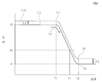
- FIG. 6 shows a process of forming the semiconductor layer 7 on the surface of the substrate 6 of the film forming apparatus 1 as a comparative example to be compared with the temperature measurement method of the embodiment of the present invention.
- Fig. 6 shows a temperature measurement method for providing a single laser beam of a predetermined wavelength ⁇ 1.
- the horizontal axis represents the temperature of the semiconductor layer 7
- the vertical axis represents the detected light amount when the laser light irregularly reflected by the bottom surface 6 a of the substrate 6 and the surface 7 a of the semiconductor layer 7 is received by the light receiving unit 11 Indicates a change in
- the change line (i) shown in FIG. 6 indicates the temperature change of the semiconductor layer 7 and the amount of light detected by the light receiving portion 11 under the almost ideal conditions where the irregularly reflected light R2 of the surface 7a of the semiconductor layer 7 is not generated. It shows the relationship with
- the change line (i) when the temperature of the semiconductor layer 7 is low, the diffuse reflection light R1 irregularly reflected by the bottom surface 6a of the substrate 6 shown in FIG. 4 is high because the light transmittance of the semiconductor layer 7 is high.
- the semiconductor layer 7 is transmitted at a high rate. Therefore, the light amount of the irregularly reflected light of the laser light received by the light receiving unit 11 is large, and the detected light amount is D2.
- the temperature of the semiconductor layer 7 rises and reaches T1
- the light transmittance of the semiconductor layer 7 starts to decrease, so the amount of irregularly reflected light received by the light receiving unit 11 begins to attenuate from D2.
- the temperature of the semiconductor layer 7 rises to T2
- the light transmittance of the semiconductor layer 7 becomes minimum, and the detected light amount of irregularly reflected light received by the light receiving unit 11 decreases to D1.
- the attenuation start point the point (a) at which the detected light quantity of diffusely reflected light in the light receiving unit 11 starts to decrease
- the detected light quantity at the attenuation start point (a) D2 is called the detected light quantity of the maximum value.
- a point (b) when attenuation of the detected light amount of diffusely reflected light in the light receiving unit 11 ends is called an attenuation end point
- a detected light amount D1 at the attenuation end point (b) is called a detected light amount of a minimum value.
- the optical characteristics of the substrate 6 and the semiconductor layer 7 easily change due to temperature conditions and the like, and the direction and the surface roughness of the surface 7 a of the semiconductor layer 7 also change easily. Furthermore, when the substrate 6 is placed in the chamber 2, an error is likely to occur in the facing angle between the surface 6 a of the substrate 6 and the perpendicular Lv. If the irregular reflection characteristics of the laser light fluctuate due to these various conditions, even when the light transmittance of the same semiconductor layer 7 is observed using the laser light of the same wavelength ⁇ 1, the light receiving unit 11 detects it.
- the variation of the detected light quantity can not be along the ideal variation line (i) shown in FIG. 6, but the variation quantities ⁇ 1 and ⁇ 2 are generated to show a variation like a dashed variation line (ii). Become.
- the light transmittance of the semiconductor layer 7 does not change if the temperature and the wavelength are the same, but if various optical conditions such as irregular reflection conditions other than the light transmittance change, The detected light amount of the irregularly reflected light of the laser light in the light receiving unit 11 fluctuates.
- the temperature Tx between T2 and T1 is determined from the monitor value of the temperature during film formation. It can not be calculated, and control to maintain the temperature of the semiconductor layer 7 at the temperature Tx can not be performed.
- the temperature of the semiconductor layer 7 can be increased to a value exceeding T2 by using at least two types of laser beams having different wavelengths. Even without raising the temperature, the temperature Tx between T2 and T1 can be calculated immediately from the monitor value of the detected light amount of the laser light in the light receiving unit 11.
- the first laser light source 22 of the light emitting device 21 shown in FIG. 2 emits the laser light L1 of the first wavelength
- the second light source 23 emits the laser light of the second wavelength.
- L2 is emitted, and the respective laser beams L1 and L2 are given to the semiconductor layer 7 through the same path Ld.
- the change line (iii) in FIG. 7 is the amount of light detected when the laser beam L1 of the first wavelength is given to the semiconductor layer 7 on the substrate 6 and the irregularly reflected lights R1 and R2 are received by the light receiving unit 11.
- the change line (iv) shows the relationship between the temperature of the semiconductor layer 7 and the laser beam L2 of the second wavelength given to the semiconductor layer 7 on the substrate 6, and the irregularly reflected lights R1 and R2 are received by the light receiving unit 11.
- 7 shows the relationship between the detected light quantity and the temperature of the semiconductor layer 7 at the time of
- the wavelength of the laser light L1 of the first wavelength is selected so that the temperature of the conductor layer 7 at the attenuation start point (e) is T3 and the temperature at the attenuation end point (f) is T4. .
- the wavelength of the laser beam L2 of the second wavelength is selected so that the temperature at the attenuation start point (g) is T5 and the temperature at the attenuation end point (h) is T6.
- the temperature T3 to T4 is a first temperature range in which the transmission amount of the laser light L1 of the first wavelength is attenuated
- the temperature T5 to T6 is the light of the laser light L2 of the second wavelength
- the second temperature range is a region where the temperature is higher than the first temperature range.
- the laser beam L1 of the first wavelength is selected according to the material of the semiconductor layer 7.
- the first temperature range can be set by selecting the wavelength
- the second temperature range can be set by selecting the wavelength of the laser light L2 of the second wavelength according to the material.
- the laser light L1 of the first wavelength and the laser light L2 of the second wavelength are given to the semiconductor layer 7 from the same route Ld, the influence of the irregular reflection surface of the bottom surface 6a of the substrate 6 or the surface 7a of the semiconductor layer 7
- the laser light L1 of the first wavelength and the laser light of the second wavelength affect the light transmission and reflection, such as the influence of the surface roughness and the error of the facing angle of the surface 7a of the semiconductor layer 7 with respect to the perpendicular Lv. It will be received equally with L2. That is, the ratio of the variation amounts ⁇ 1 and ⁇ 2 to the detected light amount shown in FIG. 6 is the same for the laser light L1 of the first wavelength and the laser light L2 of the second wavelength.
- the light emission intensity of the laser light L1 of the first wavelength and the light emission intensity of the laser light L2 of the second wavelength in the light emitting device 21 are equal, and the light reception sensitivity of the laser light L1 of the first wavelength If the light receiving sensitivity of the laser light L2 of the second wavelength is equal, as shown in FIG. 7, the detected light quantity of the maximum value of the laser light L1 of the first wavelength and the maximum light of the laser light L2 of the second wavelength The amount of light detected should be the same D4, and the attenuation of the laser light L1 of the first wavelength and the attenuation of the laser light L2 of the second wavelength should be the same (D4-D3).
- the two laser beams have variations in light emission intensity and the light receiving sensitivities of the respective laser beams also vary, it is necessary to perform the initialization operation when the film forming apparatus 1 is started. .
- the substrate 6 on which the semiconductor layer for sample is previously formed is placed on the table 3 in the chamber 2 and the temperatures of the substrate 6 and the semiconductor layer 7 are monitored while monitoring the temperature by the pyrometer 10
- the laser light L1 of the first wavelength and the laser light L2 of the second wavelength are given to the semiconductor layer for sample while being gradually raised.
- T3-T4 the change in the detected light quantity of the laser light L1 of the first wavelength and the temperature when the temperature exceeds the second temperature range (T5-T6)
- T5-T6 The change of the detected light quantity of the laser light L2 of the second wavelength is measured.
- the attenuation width of the detected light quantity of the laser light L1 of the first wavelength in the first temperature range and the attenuation width of the detected light quantity of the laser light of the second wavelength in the second temperature range make adjustments on the circuit or perform calibration on software so that the same.
- the first laser light source 22 shown in FIG.
- the laser light L1 of the first wavelength irregularly reflected from the surface of the light source is detected by the light receiving unit 11.
- the second laser light source 23 is turned on, and the laser beam L2 of the second wavelength irregularly reflected from the bottom surface 6a of the substrate 6 or the surface of the substrate 6 is detected by the light receiving unit 11.
- the detected light amount when the first laser light source 22 is turned on and the detected light amount when the second laser light source 23 is turned on become the same level. Good.
- the monitor value of the detected light quantity of the laser light in the light receiving unit 11 is obtained without raising the temperature of the semiconductor layer 7 to a temperature higher than T6 shown in FIG. It is possible to immediately calculate the temperature Ty between the temperature T5 which is the second temperature range and the temperature T6.
- the detected light quantity of the laser light L1 of the first wavelength exceeds the attenuation start point (e) and attenuates It reaches the end point (f).
- the detected light amount of the laser light L2 of the second wavelength is not attenuated.
- the light receiving unit 11 is provided with the attenuation (D4-D3) of the detected light quantity of the laser light L1 of the first wavelength. The signal is detected by the processing circuit unit 12 and sent to the central control unit 30 via the temperature detection unit 33 and held.
- the central control device 30 attenuates the detection light amount of the laser light L2 of the second wavelength.
- the temperature at the time of measurement of the semiconductor layer 7 is measured from (the temperature of the maximum value of the second range) + (the temperature difference of the second range) ⁇ ⁇ (the attenuation start point of the transmission amount of light of the second wavelength). It can be calculated from the amount of attenuation up to time) / (the attenuation width of the detected light amount related to the light of the first wavelength) ⁇ .
- the temperature of the semiconductor layer 7 is monitored from T5 by monitoring the temperature after the laser light L2 of the second wavelength exceeds the attenuation start point (g). It is possible to control the temperature Ty during T6.
- the relationship between the light transmittance and the temperature at that time when the semiconductor layer 7 is irradiated with the laser beam L2 of the second wavelength can be set by the relationship between the semiconductor material and the wavelength of the laser beam L2.
- the semiconductor layer 7 is GaN (gallium nitride) and 445 nm is selected as the wavelength of the laser light L2 of the second wavelength
- the temperature T5 at the attenuation start point (g) is attenuated at about 800 ° C.
- the temperature T6 in h) can be set to about 900.degree.
- the film formation temperature of the semiconductor layer 7 can always be controlled to a predetermined temperature between 800 ° C. and 900 ° C.
- the wavelength of the laser light L1 of the first wavelength is relatively wide as long as the temperature T4 of the attenuation end point (f) is lower than the temperature T5 of the attenuation start point (g) of the laser light L2 of the second wavelength. It can be decided from the selection range.
- an infrared ray emitted from the surface of the substrate 6 and the semiconductor layer 7 is detected by the pyrometer 10 as an example of a temperature change measuring apparatus, and a detection output of the infrared is sent to the temperature detecting apparatus 33.
- the temperature of the semiconductor layer 7 is measured indirectly. Comparison of the temperature information obtained by the detection of the infrared light with the temperature calculated using the laser light L1 of the first wavelength and the laser light L2 of the second wavelength, the pyrometer 10 obtained by the infrared detection Temperature information can be calibrated. Alternatively, by using both the temperature calculated using the laser light L1 of the first wavelength and the laser light L2 of the second wavelength and the temperature information obtained by the detection of infrared light, the temperature control can be performed with higher accuracy. It will be possible to
- FIG. 8 is a temperature at which the temperature of the semiconductor layer 7 is controlled to be a predetermined temperature Ty within the second temperature range (T6-T5) during the film formation of the semiconductor layer 7 by the film forming apparatus 1. It shows a control method.
- a change line (v) indicates the change in the amount of detected light detected by the light receiving unit 11 with the laser light L1 of the first wavelength, and the change in the amount of detected light detected by the light receiving unit 11 with the laser light L2 with the second wavelength Is indicated by the change line (vi).
- the temperature T of the semiconductor layer 7 rises.
- the attenuation width (D6-D5) of the laser light L1 of the first wavelength is determined.
- the second light detector 11 detects the second light at any time thereafter.
- the actual temperature of the semiconductor layer 7 is immediately calculated from the monitor value of the light reception amount of the laser light L2 of the wavelength of and the attenuation width (D6-D5) of the laser light L1 of the first wavelength already measured. Can. Therefore, after the detected light quantity of the laser light L2 of the second wavelength becomes Dc between D6 and D5 at time ⁇ b, the heater 3a is controlled by the heating control device 31, and the monitor value of the detected light quantity is Dc. If maintained, it is possible to keep setting the temperature of the semiconductor layer 7 to the temperature Ty within the second temperature range (T5-T6) which is optimum for film formation.
- the detected light amount of the laser light L2 of the second wavelength is monitored.
- the temperature of the semiconductor layer 7 can be set to the temperature Ty that is optimum for film formation, without raising the temperature of the semiconductor layer 7 beyond the second temperature range.
- FIG. 9 and FIG. 10 show a case in which the detected light amount detected by the light receiving element 11 changes while the temperature of the semiconductor layer 7 is controlled to become the optimum value Ty after the time ⁇ b. ing.
- the detected light amount of the laser light L2 of the second wavelength fluctuates as indicated by ⁇ without being stabilized at Dc.
- the detected light amount of the laser light L1 of the first wavelength is also not stable at the minimum value D5, and the same variation ⁇ as that of the above-mentioned ⁇ occurs.
- the surface roughness of the surface 7a of the semiconductor layer 7 changes Then, it can be determined that the incident condition and the reflection condition of the laser beam to the semiconductor layer 7 are changed due to, for example, the irregularly reflected light R2 changing.
- the change Tz in the temperature of the semiconductor layer 7 is not a change in the light transmission condition or the reflection condition for the laser light of two wavelengths unless a large change is shown after that. .
- the detection light amount of the laser light L1 of the first wavelength exceeds the attenuation end point (m)
- the detection light amount of the laser light L1 of the first wavelength and the detection light amount of the laser light L2 of the second wavelength are By monitoring both, it can be determined whether the temperature of the semiconductor layer 7 has changed or whether an optical change has occurred in the semiconductor layer 7.
- a part of the surface 7a may evaporate to roughen the surface, and the irregularly reflected light R2 on the surface 7a may increase.
- the phenomenon can be known, and by controlling the introduction amount of the source gas 5 and the heating temperature, it is possible to suppress the occurrence of surface roughness of the surface 7 a. Alternatively, control to intentionally cause surface roughness on the surface 7 a of the semiconductor layer 7 is also possible.
- the magnitude or surface roughness of the surface 7 a of the semiconductor layer 7 is at least one of the change ⁇ of the detected light quantity of the laser light L 1 of the first wavelength and the change ⁇ of the detected light quantity of the laser light L 2 of the second wavelength
- the size of the surface roughness can be determined. Thereby, the size of the actual surface roughness can be estimated as a numerical value, or can be used for relatively rough determination of whether the surface roughness is within the allowable value.
- the light detection device 10 is made to face the surface side of the substrate 6 as in FIG. 1 except that the light emission device 21 emits laser light L1 and L2 of two wavelengths. It is possible to have a structure in which the back surface of the substrate 6 is made to face. In this case, the laser light L1 of the first wavelength and the laser light L2 of the second wavelength are incident on the bottom surface 6a of the substrate 6, transmitted through the substrate 6, transmitted through the semiconductor layer 7, and received by the light receiving unit 11. Be done.
- the surface roughness of the surface of the semiconductor layer 7 and the like other than the change in the light transmittance of the semiconductor layer The optical change of the semiconductor layer 7 can be canceled and the temperature of the semiconductor layer 7 can be measured as needed.
Landscapes
- Chemical & Material Sciences (AREA)
- Organic Chemistry (AREA)
- Chemical Kinetics & Catalysis (AREA)
- General Chemical & Material Sciences (AREA)
- Engineering & Computer Science (AREA)
- Materials Engineering (AREA)
- Metallurgy (AREA)
- General Physics & Mathematics (AREA)
- Physics & Mathematics (AREA)
- Crystallography & Structural Chemistry (AREA)
- Mechanical Engineering (AREA)
- Testing Or Measuring Of Semiconductors Or The Like (AREA)
- Measuring Temperature Or Quantity Of Heat (AREA)
- Investigating Or Analysing Materials By Optical Means (AREA)
Abstract
Description
半導体層の温度が上昇して第1の範囲の温度になると前記半導体層に対する透過率が減衰する第1の波長の光と、前記半導体層の温度が前記第1の範囲よりも高い第2の範囲になると前記半導体層に対する光の透過率が減衰する第2の波長の光とを使用し、
第1の波長の光と第2の波長を同じ経路に沿って前記半導体層に与えるとともに、前記半導体に対向する光検出装置で前記第1の波長の光と前記第2の波長の光量を検知し、
前記半導体層の温度が前記第1の範囲を超えて上昇して第1の波長の光の検知光量が減衰した後で、さらに第2の波長の光の検知光量が減衰し始めた後の測定時に、その測定時の第2の波長の検知光量と、第1の波長の光の検知光量の減衰幅とから、半導体層の前記第2の範囲内での温度を算出することを特徴とするものである。
前記半導体層の表面に第1の波長の光と第2の波長の光を与え、前記半導体層の表面に対向する前記光検出装置で、前記半導体層の内部を通過する乱反射光と前記半導体層の表面で反射される乱反射光とを検知するものである。
半導体層の温度が上昇して第1の範囲の温度になると前記半導体層に対する透過率が減衰する第1の波長の光と、前記半導体層の温度が前記第1の範囲よりも高い第2の範囲になると前記半導体層に対する光の透過率が減衰する第2の波長の光とを使用し、
第1の波長の光と第2の波長を同じ経路に沿って前記半導体層に与えるとともに、前記半導体に対向する光検出装置で前記第1の波長の光と前記第2の波長の光量を検知し、
前記半導体層の温度が前記第1の範囲を超えて上昇して第1の波長の光の検知光量が減衰した後に、第2の波長の光の検知光量を監視し、第2の波長の光の検知光量が変化したら、そのときの第1の波長の光の検知光量の変化を参照して、第2の波長の光の検知光量の変化が、半導体層の温度変化によるものかそれ以外の要因によるものであるかを判定することを特徴とするものである。
前記半導体層の表面に第1の波長の光と第2の波長の光を与え、前記半導体層の表面に対向する前記光検出装置で、前記半導体層の内部を通過する乱反射光と前記半導体層の表面で反射される乱反射光とを検知するものである。
半導体層の温度が上昇して第1の範囲の温度になると前記半導体層に対する透過率が減衰する第1の波長の光と、前記半導体層の温度が前記第1の範囲よりも高い第2の範囲になると前記半導体層に対する光の透過率が減衰する第2の波長の光とを与える発光装置と、
第1の波長の光と第2の波長の光を検知する光検出装置とが設けられ、
前記発光装置と前記光検出装置が半導体の表面に対向して、第1の波長の光と第2の波長の光が同じ経路に沿って前記表面に与えられ、前記半導体層の内部を通過する乱反射光と前記表面からの乱反射光とが前記光検出装置で検知され、
前記光検出装置で検知された第1の波長の光の検知光量と第2の波長の光の検知光量とから、前記半導体層の温度を算出する制御装置が設けられていることを特徴とするものである。
第1の波長の光の検知光量の変化と第2の波長の光の検知光量の少なくとも一方から、半導体層の表面粗さが算出される。
前記受光部11は、パイロメータ10として赤外線を受光するために使用されるとともに、底面6aと表面7aで乱反射したレーザ光を受光する光検出装置としても機能している。受光部11では、加熱された基板6や半導体層7から発せられる赤外線と、基板6や半導体層7で反射されたレーザ光の乱反射光R1,R2とが、異なる時刻に交互に検出される。さらに、2つのレーザ光源22,23の点灯のタイミングに合わせて、受光部11での受光信号が時分割されて、第1の波長のレーザ光L1と第2の波長のレーザ光L2が異なるタイミングで検知される。したがって、受光部11では、赤外線および第1の波長のレーザ光L1と第2の波長のレーザ光L2とが互いに干渉することなく区別して検知される。
Tx=T1+(T2-T1)×{(D2-Da)/(D2-D1)}
Ty=T5+(T6-T5)×{(D4-Db)/(D4-D3)}
2 チャンバ
3 テーブル
6 基板
7 半導体層
8 第1の窓
9 第2の窓
10 パイロメータ
11 受光部
13 第1の受光素子
14 第2の受光素子
15 波長フィルタ
16 光検出装置
20 温度測定装置
21 発光装置
22 第1のレーザ光源
23 第2のレーザ光源
L1 第1の波長のレーザ光
L2 第2の波長のレーザ光
T3-T4 第1の温度範囲
T5-T6 第2の温度範囲
(e)(g) 減衰始点
(f)(h) 減衰終点
Claims (14)
- チャンバ内で成膜されている半導体層の温度を測定する温度測定方法において、
半導体層の温度が上昇して第1の範囲の温度になると前記半導体層に対する透過率が減衰する第1の波長の光と、前記半導体層の温度が前記第1の範囲よりも高い第2の範囲になると前記半導体層に対する光の透過率が減衰する第2の波長の光とを使用し、
第1の波長の光と第2の波長を同じ経路に沿って前記半導体層に与えるとともに、前記半導体に対向する光検出装置で前記第1の波長の光と前記第2の波長の光量を検知し、
前記半導体層の温度が前記第1の範囲を超えて上昇して第1の波長の光の検知光量が減衰した後で、さらに第2の波長の光の検知光量が減衰し始めた後の測定時に、その測定時の第2の波長の検知光量と、第1の波長の光の検知光量の減衰幅とから、半導体層の前記第2の範囲内での温度を算出することを特徴とする半導体層の温度測定方法。 - 前記半導体層の前記測定時の温度を、(第2の範囲の極大値の温度)+(第2の範囲の温度差)×{(第2の波長の光の検知光量の減衰始点から測定時までの減衰量)/(第1の波長の光の検知光量の減衰幅)}から算出する請求項1記載の半導体層の温度測定方法。
- 前記基板上に半導体層が成膜されている途中の前記測定時に得られた第2の波長の光の検知光量と、第1の波長の光の検知光量の減衰幅とから、成膜途中の半導体層の温度を算出して、その温度が前記第2の範囲内の所定値となるように前記基板の加熱温度を制御する請求項1または2記載の半導体層の温度測定方法。
- 前記チャンバ内に設けられた透明基板を加熱しながら原料分子を供給して前記基板上に半導体層を成膜し、
前記半導体層の表面に第1の波長の光と第2の波長の光を与え、前記半導体層の表面に対向する前記光検出装置で、前記半導体層の内部を通過する乱反射光と前記半導体層の表面で反射される乱反射光とを検知する請求項1ないし3のいずれかに記載の半導体層の温度測定方法。
- 半導体層から発せられる赤外線を測定して半導体層の温度を測定する温度変化測定装置を使用し、前記測定時に算出された前記第2の範囲内の温度で、前記温度変化測定装置の測定誤差を較正する請求項1ないし4のいずれかに記載の半導体層の温度測定方法。
- チャンバ内で成膜されている半導体層の温度を測定する温度測定方法において、
半導体層の温度が上昇して第1の範囲の温度になると前記半導体層に対する透過率が減衰する第1の波長の光と、前記半導体層の温度が前記第1の範囲よりも高い第2の範囲になると前記半導体層に対する光の透過率が減衰する第2の波長の光とを使用し、
第1の波長の光と第2の波長を同じ経路に沿って前記半導体層に与えるとともに、前記半導体に対向する光検出装置で前記第1の波長の光と前記第2の波長の光量を検知し、
前記半導体層の温度が前記第1の範囲を超えて上昇して第1の波長の光の検知光量が減衰した後に、第2の波長の光の検知光量を監視し、第2の波長の光の検知光量が変化したら、そのときの第1の波長の光の検知光量の変化を参照して、第2の波長の光の検知光量の変化が、半導体層の温度変化によるものかそれ以外の要因によるものであるかを判定することを特徴とする半導体層の温度測定方法。 - 第2の波長の光の検知光量が変化したときに、第1の波長の光検知光量も変化したら、第2の波長の光の検知光量の変化が、半導体層の温度変化以外の要因によるものであると判定する請求項6記載の半導体層の温度測定方法。
- 第1の波長の光の検知光量の変化と第2の波長の光の検知光量の変化との少なくとも一方から、半導体層の表面粗さを求める請求項7記載の半導体層の温度測定方法。
- 第2の波長の光の検知光量が変化しているときに、第1の波長の光の検知光量が変化しないときは、第2の波長の光の検知光量の変化が、半導体層の温度変化によるものであると判定する請求項6記載の半導体層の温度測定方法。
- 前記チャンバ内に設けられた透明基板を加熱しながら原料分子を供給して前記基板上に半導体層を成膜し、
前記半導体層の表面に第1の波長の光と第2の波長の光を与え、前記半導体層の表面に対向する前記光検出装置で、前記半導体層の内部を通過する乱反射光と前記半導体層の表面で反射される乱反射光とを検知する請求項6ないし9のいずれかに記載の半導体層の温度測定方法。
- チャンバ内で成膜されている半導体層の温度を測定する温度測定装置において、
半導体層の温度が上昇して第1の範囲の温度になると前記半導体層に対する透過率が減衰する第1の波長の光と、前記半導体層の温度が前記第1の範囲よりも高い第2の範囲になると前記半導体層に対する光の透過率が減衰する第2の波長の光とを与える発光装置と、
第1の波長の光と第2の波長の光を検知する光検出装置とが設けられ、
前記発光装置と前記光検出装置が半導体の表面に対向して、第1の波長の光と第2の波長の光が同じ経路に沿って前記表面に与えられ、前記半導体層の内部を通過する乱反射光と前記表面からの乱反射光とが前記光検出装置で検知され、
前記光検出装置で検知された第1の波長の光の検知光量と第2の波長の光の検知光量とから、前記半導体層の温度を算出する制御装置が設けられていることを特徴とする半導体層の温度測定装置。
- 前記制御装置では、前記半導体層の温度が前記第1の範囲を超えて上昇して第1の波長の光の検知光量が減衰した後で、さらに第2の波長の光の検知光量が減衰し始めた後の測定時に、その測定時の第2の波長の検知光量と、第1の波長の光の検知光量の減衰幅とから、半導体層の前記第2の範囲内での温度が算出される請求項11記載の半導体層の温度測定装置。
- 前記制御装置では、前記半導体層の温度が前記第1の範囲を超えて上昇して第1の波長の光の検知光量が減衰した後に、第2の波長の光の検知光量を監視し、第2の波長の光の検知光量が変化したら、そのときの第1の波長の光の検知光量の変化を参照して、第2の波長の光の検知光量の変化が、半導体層の温度変化によるものかそれ以外の要因によるものであるが判定される請求項11記載の半導体層の温度測定装置。
- 前記制御部では、第2の波長の光の検知光量と第1の波長の光の検知光量が共に変化したときに、
第1の波長の光の検知光量の変化と第2の波長の光の検知光量の少なくとも一方から、半導体層の表面粗さが算出される請求項13記載の半導体層の温度測定装置。
Priority Applications (8)
| Application Number | Priority Date | Filing Date | Title |
|---|---|---|---|
| EP11870369.3A EP2741062B1 (en) | 2011-08-02 | 2011-08-02 | Method for measuring temperature of semiconductor layer |
| CA2837164A CA2837164C (en) | 2011-08-02 | 2011-08-02 | Method and apparatus for measuring temperature of semiconductor layer |
| JP2013526678A JP5725584B2 (ja) | 2011-08-02 | 2011-08-02 | 半導体層の温度測定方法および温度測定装置 |
| CN201180071888.2A CN103649702B (zh) | 2011-08-02 | 2011-08-02 | 半导体层的温度测定方法以及温度测定装置 |
| KR1020137034382A KR101834034B1 (ko) | 2011-08-02 | 2011-08-02 | 반도체층의 온도 측정 방법 및 온도 측정 장치 |
| PCT/JP2011/067678 WO2013018197A1 (ja) | 2011-08-02 | 2011-08-02 | 半導体層の温度測定方法および温度測定装置 |
| US14/126,010 US9823132B2 (en) | 2011-08-02 | 2011-08-02 | Method and apparatus for measuring temperature of semiconductor layer |
| TW101126472A TWI557399B (zh) | 2011-08-02 | 2012-07-23 | Temperature measurement method and temperature measuring device for semiconductor layer |
Applications Claiming Priority (1)
| Application Number | Priority Date | Filing Date | Title |
|---|---|---|---|
| PCT/JP2011/067678 WO2013018197A1 (ja) | 2011-08-02 | 2011-08-02 | 半導体層の温度測定方法および温度測定装置 |
Publications (1)
| Publication Number | Publication Date |
|---|---|
| WO2013018197A1 true WO2013018197A1 (ja) | 2013-02-07 |
Family
ID=47628760
Family Applications (1)
| Application Number | Title | Priority Date | Filing Date |
|---|---|---|---|
| PCT/JP2011/067678 Ceased WO2013018197A1 (ja) | 2011-08-02 | 2011-08-02 | 半導体層の温度測定方法および温度測定装置 |
Country Status (8)
| Country | Link |
|---|---|
| US (1) | US9823132B2 (ja) |
| EP (1) | EP2741062B1 (ja) |
| JP (1) | JP5725584B2 (ja) |
| KR (1) | KR101834034B1 (ja) |
| CN (1) | CN103649702B (ja) |
| CA (1) | CA2837164C (ja) |
| TW (1) | TWI557399B (ja) |
| WO (1) | WO2013018197A1 (ja) |
Families Citing this family (8)
| Publication number | Priority date | Publication date | Assignee | Title |
|---|---|---|---|---|
| US10571337B2 (en) | 2017-05-26 | 2020-02-25 | Applied Materials, Inc. | Thermal cooling member with low temperature control |
| SG10201705708YA (en) | 2017-05-26 | 2018-12-28 | Applied Materials Inc | Detector for low temperature transmission pyrometry |
| US10281335B2 (en) | 2017-05-26 | 2019-05-07 | Applied Materials, Inc. | Pulsed radiation sources for transmission pyrometry |
| US10845249B2 (en) | 2017-05-26 | 2020-11-24 | Applied Materials, Inc. | Continuous spectra transmission pyrometry |
| CN109443589A (zh) * | 2018-08-29 | 2019-03-08 | 宁波中车时代传感技术有限公司 | 一种igbt模块及igbt模块的温度监测系统 |
| JP7362505B2 (ja) * | 2020-02-20 | 2023-10-17 | 東京エレクトロン株式会社 | 基板液処理装置及び液体吐出評価方法 |
| CN111485284B (zh) * | 2020-05-26 | 2025-05-16 | 江西乾照光电有限公司 | 沉积设备及沉积方法、沉积设备中温度检测点的确定方法 |
| EP4567390A1 (de) | 2023-12-08 | 2025-06-11 | Justus-Liebig-Universität Gießen | Verfahren zur temperaturbestimmung eines lasermediums |
Citations (6)
| Publication number | Priority date | Publication date | Assignee | Title |
|---|---|---|---|---|
| JPH03216526A (ja) * | 1989-11-22 | 1991-09-24 | Res Corp Technol Inc | 光の透過率による半導体物質の温度の測定法 |
| JP2001289714A (ja) | 2000-04-07 | 2001-10-19 | Matsushita Electric Ind Co Ltd | 基板の温度計測方法及び計測装置、並びに基板の処理装置 |
| JP2002122480A (ja) | 2000-10-12 | 2002-04-26 | Toshiba Corp | 温度測定方法および装置、並びにプラズマ処理装置 |
| JP2002367907A (ja) | 2001-06-04 | 2002-12-20 | Inst Of Physical & Chemical Res | 結晶成長装置および結晶成長方法 |
| JP2003519380A (ja) * | 2000-01-05 | 2003-06-17 | 東京エレクトロン株式会社 | 透過分光を用いるウェハ帯域エッジの測定方法、及びウェハの温度均一性を制御するためのプロセス |
| WO2010073358A1 (ja) * | 2008-12-26 | 2010-07-01 | 有限会社ワイ・システムズ | 半導体成膜時の温度測定方法および温度測定装置 |
Family Cites Families (10)
| Publication number | Priority date | Publication date | Assignee | Title |
|---|---|---|---|---|
| US5229303A (en) * | 1989-08-29 | 1993-07-20 | At&T Bell Laboratories | Device processing involving an optical interferometric thermometry using the change in refractive index to measure semiconductor wafer temperature |
| US5474381A (en) | 1993-11-30 | 1995-12-12 | Texas Instruments Incorporated | Method for real-time semiconductor wafer temperature measurement based on a surface roughness characteristic of the wafer |
| US5835225A (en) * | 1994-11-30 | 1998-11-10 | Micron Technology, Inc. | Surface properties detection by reflectance metrology |
| US5618461A (en) * | 1994-11-30 | 1997-04-08 | Micron Technology, Inc. | Reflectance method for accurate process calibration in semiconductor wafer heat treatment |
| JP3366538B2 (ja) * | 1996-11-29 | 2003-01-14 | 大日本スクリーン製造株式会社 | 温度測定装置およびそれを用いた基板熱処理装置 |
| US6116779A (en) * | 1997-03-10 | 2000-09-12 | Johnson; Shane R. | Method for determining the temperature of semiconductor substrates from bandgap spectra |
| US20050106876A1 (en) * | 2003-10-09 | 2005-05-19 | Taylor Charles A.Ii | Apparatus and method for real time measurement of substrate temperatures for use in semiconductor growth and wafer processing |
| JP5076278B2 (ja) * | 2005-03-14 | 2012-11-21 | 日亜化学工業株式会社 | 電界効果トランジスタ |
| US7543981B2 (en) * | 2006-06-29 | 2009-06-09 | Mattson Technology, Inc. | Methods for determining wafer temperature |
| US8283607B2 (en) * | 2008-04-09 | 2012-10-09 | Applied Materials, Inc. | Apparatus including heating source reflective filter for pyrometry |
-
2011
- 2011-08-02 US US14/126,010 patent/US9823132B2/en not_active Expired - Fee Related
- 2011-08-02 EP EP11870369.3A patent/EP2741062B1/en not_active Not-in-force
- 2011-08-02 CA CA2837164A patent/CA2837164C/en active Active
- 2011-08-02 CN CN201180071888.2A patent/CN103649702B/zh not_active Expired - Fee Related
- 2011-08-02 KR KR1020137034382A patent/KR101834034B1/ko not_active Expired - Fee Related
- 2011-08-02 WO PCT/JP2011/067678 patent/WO2013018197A1/ja not_active Ceased
- 2011-08-02 JP JP2013526678A patent/JP5725584B2/ja active Active
-
2012
- 2012-07-23 TW TW101126472A patent/TWI557399B/zh not_active IP Right Cessation
Patent Citations (6)
| Publication number | Priority date | Publication date | Assignee | Title |
|---|---|---|---|---|
| JPH03216526A (ja) * | 1989-11-22 | 1991-09-24 | Res Corp Technol Inc | 光の透過率による半導体物質の温度の測定法 |
| JP2003519380A (ja) * | 2000-01-05 | 2003-06-17 | 東京エレクトロン株式会社 | 透過分光を用いるウェハ帯域エッジの測定方法、及びウェハの温度均一性を制御するためのプロセス |
| JP2001289714A (ja) | 2000-04-07 | 2001-10-19 | Matsushita Electric Ind Co Ltd | 基板の温度計測方法及び計測装置、並びに基板の処理装置 |
| JP2002122480A (ja) | 2000-10-12 | 2002-04-26 | Toshiba Corp | 温度測定方法および装置、並びにプラズマ処理装置 |
| JP2002367907A (ja) | 2001-06-04 | 2002-12-20 | Inst Of Physical & Chemical Res | 結晶成長装置および結晶成長方法 |
| WO2010073358A1 (ja) * | 2008-12-26 | 2010-07-01 | 有限会社ワイ・システムズ | 半導体成膜時の温度測定方法および温度測定装置 |
Non-Patent Citations (1)
| Title |
|---|
| See also references of EP2741062A4 |
Also Published As
| Publication number | Publication date |
|---|---|
| KR20140040763A (ko) | 2014-04-03 |
| TW201321730A (zh) | 2013-06-01 |
| US20140192839A1 (en) | 2014-07-10 |
| JP5725584B2 (ja) | 2015-05-27 |
| TWI557399B (zh) | 2016-11-11 |
| JPWO2013018197A1 (ja) | 2015-03-02 |
| KR101834034B1 (ko) | 2018-03-02 |
| CA2837164A1 (en) | 2013-02-07 |
| CA2837164C (en) | 2017-08-22 |
| EP2741062B1 (en) | 2017-02-01 |
| EP2741062A4 (en) | 2014-12-10 |
| EP2741062A1 (en) | 2014-06-11 |
| US9823132B2 (en) | 2017-11-21 |
| CN103649702B (zh) | 2016-08-17 |
| CN103649702A (zh) | 2014-03-19 |
Similar Documents
| Publication | Publication Date | Title |
|---|---|---|
| JP5725584B2 (ja) | 半導体層の温度測定方法および温度測定装置 | |
| JP5232250B2 (ja) | 半導体成膜時の温度測定方法 | |
| US8786841B2 (en) | Thin film temperature measurement using optical absorption edge wavelength | |
| US20250155291A1 (en) | Method for emissivity-corrected pyrometry | |
| US20250154655A1 (en) | Method for emissivity-corrected pyrometry | |
| JP2002539423A (ja) | 放射率が波長により変化する物体の温度のアクティブパイロメトリーのための方法および装置 | |
| US6062729A (en) | Rapid IR transmission thermometry for wafer temperature sensing | |
| US20030231694A1 (en) | Temperature-measuring device | |
| US20210233787A1 (en) | Warp measurement device, vapor deposition apparatus, and warp measurement method | |
| US20250003806A1 (en) | Chamber kits, systems, and methods for calibrating temperature sensors for semiconductor manufacturing | |
| JPH1062129A (ja) | 膜厚測定方法 | |
| US20250251285A1 (en) | Substrate processing systems, methods, and related apparatus and chambers, for detecting processing shifts | |
| JP2011195871A (ja) | 膜厚組成計測装置付き混合薄膜形成装置 | |
| WO2004010094A1 (en) | Emissivity corrected radiation pyrometer integral with a reflectometer and roughness sensor for remote measuring of true surface temperatures | |
| KR0138863B1 (ko) | 금속유기물 화학증착에 의한 막의 모니터링 장치 | |
| JP2970020B2 (ja) | コーティング薄膜の形成方法 | |
| JPH0560706A (ja) | ガス濃度モニタ方法及び装置 | |
| JPH06102019A (ja) | シリコン薄膜の膜厚または屈折率測定方法およびその装置 | |
| JPH05166905A (ja) | 半導体プロセス終点判定用モニタ装置 |
Legal Events
| Date | Code | Title | Description |
|---|---|---|---|
| 121 | Ep: the epo has been informed by wipo that ep was designated in this application |
Ref document number: 11870369 Country of ref document: EP Kind code of ref document: A1 |
|
| REEP | Request for entry into the european phase |
Ref document number: 2011870369 Country of ref document: EP |
|
| WWE | Wipo information: entry into national phase |
Ref document number: 2011870369 Country of ref document: EP |
|
| ENP | Entry into the national phase |
Ref document number: 2837164 Country of ref document: CA |
|
| ENP | Entry into the national phase |
Ref document number: 20137034382 Country of ref document: KR Kind code of ref document: A |
|
| NENP | Non-entry into the national phase |
Ref country code: DE |
|
| ENP | Entry into the national phase |
Ref document number: 2013526678 Country of ref document: JP Kind code of ref document: A |
|
| WWE | Wipo information: entry into national phase |
Ref document number: 14126010 Country of ref document: US |