WO2013021614A1 - 圧電体素子 - Google Patents
圧電体素子 Download PDFInfo
- Publication number
- WO2013021614A1 WO2013021614A1 PCT/JP2012/004978 JP2012004978W WO2013021614A1 WO 2013021614 A1 WO2013021614 A1 WO 2013021614A1 JP 2012004978 W JP2012004978 W JP 2012004978W WO 2013021614 A1 WO2013021614 A1 WO 2013021614A1
- Authority
- WO
- WIPO (PCT)
- Prior art keywords
- electrode layer
- lower electrode
- piezoelectric
- layer
- substrate
- Prior art date
- Legal status (The legal status is an assumption and is not a legal conclusion. Google has not performed a legal analysis and makes no representation as to the accuracy of the status listed.)
- Ceased
Links
Images




Classifications
-
- H—ELECTRICITY
- H10—SEMICONDUCTOR DEVICES; ELECTRIC SOLID-STATE DEVICES NOT OTHERWISE PROVIDED FOR
- H10N—ELECTRIC SOLID-STATE DEVICES NOT OTHERWISE PROVIDED FOR
- H10N30/00—Piezoelectric or electrostrictive devices
- H10N30/80—Constructional details
- H10N30/87—Electrodes or interconnections, e.g. leads or terminals
-
- H—ELECTRICITY
- H10—SEMICONDUCTOR DEVICES; ELECTRIC SOLID-STATE DEVICES NOT OTHERWISE PROVIDED FOR
- H10N—ELECTRIC SOLID-STATE DEVICES NOT OTHERWISE PROVIDED FOR
- H10N30/00—Piezoelectric or electrostrictive devices
- H10N30/704—Piezoelectric or electrostrictive devices based on piezoelectric or electrostrictive films or coatings
- H10N30/706—Piezoelectric or electrostrictive devices based on piezoelectric or electrostrictive films or coatings characterised by the underlying bases, e.g. substrates
-
- H—ELECTRICITY
- H10—SEMICONDUCTOR DEVICES; ELECTRIC SOLID-STATE DEVICES NOT OTHERWISE PROVIDED FOR
- H10N—ELECTRIC SOLID-STATE DEVICES NOT OTHERWISE PROVIDED FOR
- H10N30/00—Piezoelectric or electrostrictive devices
- H10N30/704—Piezoelectric or electrostrictive devices based on piezoelectric or electrostrictive films or coatings
- H10N30/706—Piezoelectric or electrostrictive devices based on piezoelectric or electrostrictive films or coatings characterised by the underlying bases, e.g. substrates
- H10N30/708—Intermediate layers, e.g. barrier, adhesion or growth control buffer layers
-
- H—ELECTRICITY
- H10—SEMICONDUCTOR DEVICES; ELECTRIC SOLID-STATE DEVICES NOT OTHERWISE PROVIDED FOR
- H10N—ELECTRIC SOLID-STATE DEVICES NOT OTHERWISE PROVIDED FOR
- H10N30/00—Piezoelectric or electrostrictive devices
- H10N30/80—Constructional details
- H10N30/85—Piezoelectric or electrostrictive active materials
- H10N30/853—Ceramic compositions
- H10N30/8548—Lead-based oxides
- H10N30/8554—Lead-zirconium titanate [PZT] based
-
- H—ELECTRICITY
- H10—SEMICONDUCTOR DEVICES; ELECTRIC SOLID-STATE DEVICES NOT OTHERWISE PROVIDED FOR
- H10N—ELECTRIC SOLID-STATE DEVICES NOT OTHERWISE PROVIDED FOR
- H10N30/00—Piezoelectric or electrostrictive devices
- H10N30/80—Constructional details
- H10N30/87—Electrodes or interconnections, e.g. leads or terminals
- H10N30/877—Conductive materials
- H10N30/878—Conductive materials the principal material being non-metallic, e.g. oxide or carbon based
Definitions
- the present invention relates to a piezoelectric element using a piezoelectric body having an electromechanical conversion function as a drive source.
- An oxide ferroelectric thin film having a perovskite structure is represented by a general formula ABO 3 and exhibits excellent ferroelectricity, piezoelectricity, pyroelectricity, and electro-optical properties. Therefore, this thin film is used as an effective material for a wide range of devices such as various sensors, actuators, and memories, and its range of use is expected to expand further in the future.
- PZT lead zirconate titanate
- Pb (Zr x Ti 1-x ) O 3 (0 ⁇ x ⁇ 1) hereinafter referred to as “PZT”
- PZT is used as a piezoelectric displacement element such as a piezoelectric sensor or a piezoelectric actuator.
- the piezoelectric sensor uses a ferroelectric piezoelectric effect. Ferroelectrics have spontaneous polarization inside, and generate positive and negative charges on the surface. In the steady state in the atmosphere, it is in a neutral state combined with the charge of the molecules in the atmosphere.
- the piezoelectric actuator When an external pressure is applied to the piezoelectric body, an electrical signal corresponding to the amount of pressure can be extracted from the piezoelectric body.
- the piezoelectric actuator also uses the same principle. That is, when a voltage is applied to the piezoelectric body, the piezoelectric body expands and contracts according to the voltage, and displacement can be generated in the expansion / contraction direction or a direction orthogonal to the direction.
- PZT-based thin films can be produced using vapor phase growth methods such as sputtering, Chemical Vapor Deposition (hereinafter referred to as “CVD”), Pulsed Laser Deposition (hereinafter referred to as “PLD”), and the like.
- CVD Chemical Vapor Deposition
- PLD Pulsed Laser Deposition
- CSD method a liquid phase growth method represented by a chemical solution method (Chemical Solution Deposition method, hereinafter referred to as “CSD method”), a hydrothermal synthesis method, and the like.
- CSD method is characterized by easy composition control, easy production of a thin film with good reproducibility, and low-cost production equipment and mass production.
- FIG. 9 shows the element structure of a conventional PZT thin film.
- the unimorph type piezoelectric film element 1 includes a substrate 2, a diaphragm 3, an intermediate film 4, an electrode film 5, and a piezoelectric film 6.
- the Si substrate 2 has a hollow portion 2A.
- the SiO 2 diaphragm 3 is formed by thermally oxidizing the substrate 2.
- the MgO intermediate film 4 is formed on the vibration plate 3, and the electrode film 5 is laminated thereon.
- the piezoelectric film 6 is formed by forming a PZT film without heating using RF sputtering and post-baking.
- the thermal expansion coefficient of SiO 2 constituting the diaphragm 3 is 0.2 ⁇ 10 ⁇ 6 (/ ° C.), and the Young's modulus is 7.2 ⁇ 10 10 (N / m 2 ).
- MgO has a thermal expansion coefficient of 13.0 ⁇ 10 ⁇ 6 (/ ° C.) and a Young's modulus of 20.6 ⁇ 10 10 (N / m 2 ).
- the intermediate film 4 is formed by removing the MgO film having a large thermal expansion coefficient by wet etching while leaving only the portion corresponding to the hollow portion 2A of the substrate 2. Thereafter, an electrode film 5 is formed on the intermediate film 4.
- the electrode film 5 is composed of an adhesion layer and a first electrode.
- a Ti layer having a thickness of 4 nm is formed by RF sputtering as an adhesion layer, and a Pt layer having a thickness of 150 nm serving as a first electrode is formed thereon by RF sputtering.
- the substrate heater is turned off, the Ar gas pressure is set to 3.0 Pa, and an amorphous PZT layer is formed with a thickness of 1 ⁇ m by RF sputtering.
- This amorphous PZT layer is usually crystallized by heat treatment at 650 ° C. on an MgO substrate to become a PZT film which is the piezoelectric film 6.
- the thermal expansion coefficient of PZT is 9.0 ⁇ 10 ⁇ 6 (/ ° C.) near the morphotropic phase boundary (MPB) composition, and the Young's modulus is 8.0 ⁇ 10 10 (N / m 2 ).
- the amorphous PZT layer thus formed was heated to 650 ° C. at a rate of 1 ° C. per minute in an oxygen atmosphere, and then annealed for 5 hours while maintaining the temperature at 650 ° C. And it is made to crystallize by cooling to room temperature at 1 degreeC / min like the time of temperature rising. As the cooling process proceeds from the crystallization temperature, the thermal contraction of the diaphragm 3 is very small as shown by the arrow in FIG. 9, and acts in the tensile direction with respect to the other layers.
- the intermediate layer 4 made of MgO having a large thermal expansion coefficient cancels the tension and tries to compress it.
- thermo expansion coefficient of the intermediate film 4 ⁇ Young's modulus ⁇ thickness
- thermo expansion coefficient of the diaphragm 3 ⁇ Young's modulus ⁇ thickness
- thermo expansion coefficient of the piezoelectric film 6 ⁇ Young's modulus ⁇ thickness
- thermo expansion coefficient of the piezoelectric film 6 ⁇ Young's modulus ⁇ thickness
- the diaphragm 3 is as thin as 1 ⁇ m, and the intermediate film 4 is formed only in the movable region of the diaphragm 3 that is deformed to oppose the hollow portion 2A of the substrate 2. Therefore, there are few restrictions from the diaphragm 3 in the part which opposes a partition part other than the hollow part 2A, and the diaphragm 3 which opposes the hollow part 2A of the board
- substrate 2 with respect to the big contraction of the intermediate film 4 of a cooling process is a hollow part. It is greatly deformed to the 2A side and the compression stress is not lost.
- a 90 ° domain is prevented from increasing when the piezoelectric film 6 is cooled from the firing temperature to room temperature, and a P (polarization value) -E (applied electric field) curve, which is a relationship between electric field strength and electric flux density. Shows a good squareness ratio and a high saturation electric flux density, and a good hysteresis characteristic.
- Patent Document 1 is known as prior art document information relating to this application.
- the piezoelectric element of the present invention has a substrate, a lower electrode layer, a piezoelectric layer, and an upper electrode layer.
- the lower electrode layer is fixed to the substrate, and the piezoelectric layer is formed on the lower electrode layer.
- the upper electrode layer is formed on the piezoelectric layer.
- the lower electrode layer contains pores, and the thermal expansion coefficient of the lower electrode layer is larger than the thermal expansion coefficient of the piezoelectric layer.
- the lower electrode layer has a porous structure including pores, thermal stress from the substrate can be relieved. Therefore, when a substrate having a small thermal expansion coefficient such as silicon is used, application of tensile stress to the piezoelectric layer due to restraint from the substrate can be suppressed. Furthermore, since the thermal expansion coefficient of the lower electrode layer is larger than that of the piezoelectric layer, stress in the compression direction can be applied to the piezoelectric layer by thermal stress. As a result, a piezoelectric element having high piezoelectricity can be realized.
- FIG. 1 is a cross-sectional view of a piezoelectric element according to an embodiment of the present invention.
- 2A is a view showing an AFM image of the surface of the first lower electrode layer of the piezoelectric element shown in FIG. 2B is a diagram showing an AFM image of the surface of the second lower electrode layer of the piezoelectric element shown in FIG.
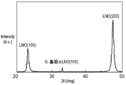
- FIG. 3 is an X-ray diffraction pattern diagram of the lower electrode layer of the piezoelectric element shown in FIG. 4 is an X-ray diffraction pattern diagram of the piezoelectric layer of the piezoelectric element shown in FIG.
- FIG. 5 is a characteristic diagram of the piezoelectric element shown in FIG. FIG.
- FIG. 6 is a cross-sectional view of another piezoelectric element according to the embodiment of the present invention.
- FIG. 7 is a characteristic diagram of still another piezoelectric element according to the embodiment of the present invention.
- FIG. 8 is a cross-sectional view of still another piezoelectric element according to the embodiment of the present invention.
- FIG. 9 is a cross-sectional view of a conventional piezoelectric element.
- FIG. 9 shows high ferroelectric characteristics, there are great restrictions on materials and element structures that can be used.
- a piezoelectric element according to an embodiment of the present invention that can obtain good piezoelectric characteristics without being limited by the element structure will be described.
- FIG. 1 is a cross-sectional view showing the structure of a piezoelectric element according to an embodiment of the present invention.
- the piezoelectric element includes a substrate 7, a diffusion prevention layer 8, a lower electrode layer 9, a piezoelectric layer 10, and an upper electrode layer 11.
- the diffusion prevention layer 8 is formed on the substrate 7, and the lower electrode layer 9 is formed on the diffusion prevention layer 8.
- the piezoelectric layer 10 is formed on the lower electrode layer 9, and the upper electrode layer 11 is formed on the piezoelectric layer 10.
- the lower electrode layer 9 includes a first lower electrode layer 9a and a second lower electrode layer 9b in order from the substrate 7 side.
- the first lower electrode layer 9a has a porous structure including pores.
- the second lower electrode layer 9b disposed on the piezoelectric layer 10 side has a dense structure with fewer pores than the first lower electrode layer 9a.
- the thermal expansion coefficients of the substrate 7, the lower electrode layer 9, and the piezoelectric layer 10 are in the relationship of substrate 7 ⁇ piezoelectric layer 10 ⁇ lower electrode layer 9. Further, in the lower electrode layer 9, since the second lower electrode layer 9b is denser than the first lower electrode layer 9a, the coefficient of thermal expansion is such that the first lower electrode layer 9a ⁇ the second lower electrode layer 9b. There is a relationship. That is, the thermal expansion coefficient of the first lower electrode layer 9 a is larger than the thermal expansion coefficient of the piezoelectric layer 10.
- the substrate 7 includes a semiconductor single crystal substrate represented by silicon, a metal material such as stainless steel, titanium, aluminum and magnesium, a glass material such as quartz glass and borosilicate glass, and a ceramic material such as alumina and zirconia. Various materials can be used. It is particularly effective to use silicon or quartz glass whose thermal expansion coefficient is sufficiently smaller than that of the piezoelectric layer 10.
- the diffusion prevention layer 8 suppresses mutual diffusion of constituent elements of the substrate 7 and the piezoelectric layer 10 as a first effect. Further, as a second effect, the oxidation of the substrate 7 is suppressed.
- a material for the diffusion prevention layer 8 an amorphous oxide material such as silicon dioxide or aluminum oxide that does not have crystal grain boundaries is desirable. Thus, even a metal material that easily oxidizes can be used as the substrate 7.
- the lower electrode layer 9 is formed of a material mainly composed of lanthanum nickelate (LaNiO 3 , hereinafter referred to as “LNO”), and is formed on the diffusion prevention layer 8 formed on the substrate 7.
- LNO lanthanum nickelate
- the lower electrode layer 9 may be formed directly on the substrate 7. Therefore, the lower electrode layer 9 may be fixed directly or indirectly to the substrate 7.
- Its resistivity is 1 ⁇ 10 ⁇ 3 ( ⁇ ⁇ cm, 300 K), and it is an oxide having metallic electrical conductivity. It has the feature that even if the temperature is changed, the transition between the metal and the insulator does not occur. .
- a material in which a part of nickel is replaced with another metal is used.
- a material in which a part of nickel is replaced with another metal is used.
- LaNiO 3 -LaFeO 3 based material obtained by substituting iron LaNiO 3 -LaAlO3 material was replaced with aluminum
- LaNiO 3 -LaMnO 3 based material obtained by substituting manganese LaNiO 3 -LaCoO 3 based material obtained by substituting cobalt .
- the piezoelectric layer 10 is rhombohedral or tetragonal (001) -oriented PZT and is formed on the lower electrode layer 9 formed on the substrate 7.
- the constituent material of the piezoelectric layer 10 may be a perovskite oxide ferroelectric material mainly composed of PZT, such as PZT containing an additive such as Sr, Nb, Mg, Zn, or Al. .
- PMN chemical formula Pb (Mg 1/3 Nb 2/3 ) O 3
- PZN chemical formula Pb (Zn 1/3 Nb 2/3 ) O 3
- Lattice matching refers to lattice matching between the PZT unit lattice and the LNO unit lattice.
- the force that tries to match the crystal lattice with the crystal lattice of the film to be deposited thereon works, and an epitaxial crystal nucleus is formed at the interface. It is reported that it is easy to form.
- the difference in lattice constant between the (001) plane and (100) plane, which are the main orientation planes of the piezoelectric layer 10, and the main orientation plane of the lower electrode layer 9 is preferably within ⁇ 10%. Within this range, the orientation of either the (001) plane or the (100) plane of the piezoelectric layer 10 can be increased. Then, an epitaxial crystal nucleus can be formed at the interface between the substrate 7 and the piezoelectric layer 10. Note that it is difficult to realize a film selectively oriented in either the (001) plane or the (100) plane in the orientation control by lattice matching.
- the upper electrode layer 11 is made of, for example, gold (Au) having a thickness of 0.3 ⁇ m.
- the material of the upper electrode layer 11 is not limited to Au but may be any conductive material, and the film thickness may be in the range of 0.1 ⁇ m to 0.5 ⁇ m.
- a method for producing the upper electrode layer 11 a vapor deposition method in which stress does not easily remain is desirable.
- a SiO 2 precursor solution is applied by spin coating.
- the spin coating method has a feature that a thin film having a uniform film thickness can be easily applied in a plane by controlling the number of revolutions per unit time.
- precursor films those that are not crystallized are referred to as precursor films.
- SiO 2 precursor solution various solutions prepared by known methods can be used. For example, tetraethoxysilane (TEOS, Si (OC 2 H 5 ) 4 ), methyltriethoxysilane (MTES, CH 3 Si (OC 2 H 5 ) 3 ), perhydropolysilazane (PHPS, SiH 2 NH), etc. are mainly used.
- a precursor solution as a component may be used.
- the SiO 2 precursor solution applied on both surfaces of the substrate 7 is dried at 150 ° C. for 10 minutes, and then main-baked at 500 ° C. for 10 minutes.
- the diffusion preventing layer 8 is formed by repeating the above steps until a desired film thickness is obtained.
- an LNO precursor solution for forming the lower electrode layer 9 is applied on the diffusion preventing layer 8 described above.
- the preparation method of this LNO precursor solution is as follows. Lanthanum nitrate hexahydrate (La (NO 3 ) 3 ⁇ 6H 2 O), nickel acetate tetrahydrate ((CH 3 COO) 2 Ni ⁇ 4H 2 O) were used as starting materials, and 2-methoxy was used as a solvent. Ethanol and 2-aminoethanol are used. Since 2-methoxyethanol slightly contains moisture, it is used after removing moisture using a molecular sieve having a pore diameter of 0.3 nm in advance.
- lanthanum nitrate hexahydrate is taken in a beaker and dried at 150 ° C. for 1 hour or longer to remove the hydrate.
- 2-methoxyethanol is added and the mixture is stirred at room temperature for 3 hours to dissolve lanthanum nitrate (solution A).
- the LNO precursor solution applied to one surface of the substrate 7 is dried at 150 ° C. for 10 minutes, and then the residual organic components are thermally decomposed by heat treatment at 350 ° C. for 10 minutes.
- the drying step is intended to remove physically adsorbed moisture in the LNO precursor solution, and the temperature is desirably higher than 100 ° C. and lower than 200 ° C. This is a process for preventing moisture from remaining in the produced film. Since the decomposition of the residual organic components in the LNO precursor solution starts at 200 ° C. or higher, it is desirable to perform drying at a temperature lower than that. Moreover, it is preferable that the temperature of a thermal decomposition process is 200 degreeC or more and less than 500 degreeC. This is a process for preventing the organic component from remaining in the produced film. However, since the crystallization of the dried LNO precursor solution greatly proceeds at 500 ° C. or higher, a temperature lower than that is desirable. .
- the process from the step of applying this LNO precursor solution on the diffusion prevention layer 8 to the thermal decomposition is repeated a plurality of times.
- rapid heating is performed using a rapid heating furnace (Rapid Thermal Annealing, hereinafter referred to as “RTA furnace”), and a crystallization process is performed.
- RTA furnace Rapid Thermal Annealing
- the conditions for the crystallization step are heating at 700 ° C. for about 5 minutes, and the rate of temperature rise is 200 ° C. per minute.
- the heating temperature in the crystallization step is preferably 500 ° C. or higher and 750 ° C. or lower. LNO crystallization is promoted at 500 ° C. or higher.
- the crystallinity of LNO decreases. Then, it is allowed to cool to room temperature.
- highly oriented LNO is obtained in the (100) plane direction.
- the steps from application to crystallization may be repeated each time.
- the lower electrode layer 9 has pores as compared with the first lower electrode layer 9a having a porous structure located on the substrate 7 side and the first lower electrode layer 9a located on the piezoelectric layer 10 side. 2 and the second lower electrode layer 9b having a dense structure.
- the coating thickness of the LNO precursor film may be adjusted by changing the coating conditions of the LNO precursor solution.
- the coating thickness of the LNO precursor solution of the first lower electrode layer 9a may be formed thicker than that of the second lower electrode layer 9b.
- 2-methoxyethanol and 2-aminoethanol having a large molecular weight are used as the solvent of the LNO precursor solution of the lower electrode layer 9 described above. These solvents generate a metal alkoxide by causing an alcohol exchange reaction with lanthanum nitrate and nickel acetate in the process of preparing the LNO precursor solution. When this alkoxide portion is decomposed by heat treatment to produce an inorganic oxide, a porous structure is formed.
- the coating thickness of the LNO precursor film is thick, it is considered that the amount of organic matter desorbed from the film during calcination increases. Furthermore, it is considered that when the LNO precursor film is thick, it is difficult to promote the densification of the film as compared with the case where the film thickness is thin. For the above reasons, it is preferable to form the second lower electrode layer 9b by repeating the steps from coating to crystallization every time to obtain a desired thickness.
- FIG. 2A shows a surface AFM image of the first lower electrode layer 9a
- FIG. 2B shows a surface AFM image of the second lower electrode layer 9b. From these results, it can be seen that the lower electrode layer 9 having a desired structure can be realized.
- the film thickness of the LNO precursor film can be reduced by increasing the rotation speed of the substrate 7.
- the film thickness can be reduced by reducing the pulling rate of the substrate 7.
- the film microstructure (number, size, distribution, etc.) of the film is controlled by adjusting the film thickness of the LNO precursor thin film, but the present invention is not limited to this method.
- the concentration of the LNO precursor solution and the type of solvent may be changed.
- the molecular weight of the LNO precursor solution for forming the first lower electrode layer 9a may be made larger than that of the LNO precursor solution for forming the second lower electrode layer 9b.
- 2-methoxyethanol and ethanol or acetic acid having a molecular weight smaller than 2-aminoethanol, or a mixture of these with water may be selected.
- the above is the formation process of the diffusion preventing layer 8 and the lower electrode layer 9.
- the first lower electrode layer 9a and the second lower electrode layer 9b are made of the same material.
- a method for manufacturing the piezoelectric layer 10 will be described.
- a PZT precursor solution is prepared, and the PZT precursor solution is applied onto the lower electrode layer 9 or the substrate 7 on which the diffusion prevention layer 8 and the lower electrode layer 9 are formed.
- the method for preparing the PZT precursor solution is as follows.
- the ethanol used in this preparation method is absolute ethanol that has been dehydrated in advance in order to prevent hydrolysis of the metal alkoxide due to water content.
- lead (II) acetate trihydrate Pb (OCOCH 3 ) 2 .3H 2 O
- Pb precursor solution is taken into a separable flask and dried for 2 hours or more to remove the hydrate.
- anhydrous ethanol is added and dissolved, and refluxed while bubbling ammonia gas to prepare a Pb precursor solution.
- This Ti—Zr precursor solution is mixed with the Pb precursor solution.
- the Pb component is made 20 mol% excess with respect to the stoichiometric composition (Pb (Zr 0.53 , Ti 0.47 ) O 3 ). This is to compensate for the shortage due to volatilization of the lead component during annealing.
- This mixed solution is refluxed at 78 ° C. for 4 hours, 0.5 mol equivalent of acetylacetone as a stabilizer is added to the total amount of metal cations, and further refluxed for 1 hour to prepare a PZT precursor solution.
- various coating methods such as a dip coating method and a spray coating method can be used as the coating method.
- the PZT precursor solution forms a wet PZT precursor film by evaporation and hydrolysis of the solvent.
- the PZT precursor film is dried for 10 minutes in a drying furnace at 115 ° C. Since decomposition of residual organic components in the PZT precursor solution starts at 200 ° C. or higher, it is desirable that the temperature of the drying process is higher than 100 ° C. and lower than 200 ° C.
- the temperature of the pre-baking step is preferably 200 ° C. or higher and lower than 500 ° C.
- the PZT precursor film is formed by repeating a plurality of times, for example, three times, from the application of the PZT precursor solution to the pre-baking step.
- a crystallization step is performed to crystallize the PZT precursor film.
- the whole including the PZT precursor film is rapidly heated using an RTA furnace.
- the heating condition in the crystallization step is about 650 ° C. for about 5 minutes, and the heating rate is 200 ° C. per minute.
- the heating temperature in the crystallization process is desirably 500 ° C. or higher and 750 ° C. or lower.
- Pb contained in the PZT precursor film evaporates at the time of crystallization, so that the crystallinity of the formed piezoelectric layer 10 is lowered.
- heating in the crystallization step is performed for at least 1 minute.
- the thickness of the piezoelectric layer 10 formed in the above process is about 50 nm to 400 nm.
- the piezoelectric layer 10 having a desired thickness is formed by repeating this step a plurality of times.
- the PZT precursor solution is applied to form a PZT precursor film, and the drying process is repeated a plurality of times, and after the PZT precursor film is formed to the desired thickness, crystallization is performed in a lump.
- a process may be performed.
- FIG. 3 is an X-ray diffraction pattern diagram showing the result of evaluating the crystallinity of the lower electrode layer 9 and FIG. 4 is the piezoelectric layer 10.
- FIG. 4 shows that the piezoelectric layer 10 (PZT thin film) is preferentially oriented in the (001) plane and the (100) plane.
- the piezoelectric layer 10 PZT thin film
- the X-ray diffraction pattern shown in FIG. Expressed as a peak. Therefore, it is difficult to obtain the respective volume fractions of the components oriented in the (001) plane and the (100) plane.
- FIG. 5 shows the results of measurement of the characteristics (PE hysteresis loop) of the piezoelectric element manufactured according to this embodiment.
- the characteristics of a conventional piezoelectric element are also shown.
- the conventional piezoelectric element has a diaphragm (SiO 2 thin film), an intermediate film (MgO thin film), and an electrode film (Pt thin film) on a substrate (Si) having a hollow portion. ) And a piezoelectric film (PZT thin film) in this order.
- the piezoelectric element of the present embodiment has a high polarization characteristic because the polarization value of the PE hysteresis loop is larger than that of the conventional piezoelectric element. Comparing the maximum polarization intensity Pmax, and the residual polarization value Pr shown in FIG. 5, the conventional piezoelectric element, + Pmax, each value of + Pr, 42 ⁇ C / cm 2, is about 16 ⁇ C / cm 2. In contrast, the piezoelectric element of the present embodiment, + Pmax, each value of + Pr, 50 ⁇ C / cm 2, shows a high value of 26 ⁇ C / cm 2. This is considered to be due to the following reason.
- the thermal stress received from the substrate 7 is relaxed.
- the thermal expansion coefficient of the second lower electrode layer 9b is larger than that of the first lower electrode layer 9a, a larger compressive stress can be applied to the piezoelectric layer 10.
- the proportion of the (001) orientation component increased, and the 90 ° domain rotation of the (100) orientation component was likely to occur, and it was considered that the component contributing to polarization increased.
- the larger the polarization value the larger the amount of displacement. Therefore, an element using the piezoelectric layer 10 can be expected to have a larger amount of displacement than the conventional one.
- elemental analysis is performed on the cross section of the piezoelectric element manufactured in this embodiment, and the in-plane distribution of Pb is examined.
- elemental analysis EDX (Energy Dispersive X-ray Spectrometry) is used.
- the lower electrode layer 9 is compared with a piezoelectric element in which a piezoelectric layer 10 is formed on a porous LNO thin film including pores.
- Pb of the piezoelectric layer 10 is diffused to the diffusion preventing layer 8 in this comparative piezoelectric element.
- the diffusion of Pb is greatly suppressed, and the diffusion of Pb cannot be confirmed from the analysis result.
- the diffusion preventing layer 8 and the Pb on the substrate 7 can be formed. Diffusion can be suppressed.
- the first lower electrode layer 9a having a porous film structure including pores on the substrate 7 side the thermal stress caused by the difference in thermal expansion coefficient from the substrate 7 in the crystallization process is alleviated, and the piezoelectric characteristics are reduced. Can be formed.
- a piezoelectric element can be manufactured by appropriately forming the upper electrode layer 11 on the piezoelectric layer 10 formed by the above manufacturing method.
- a method for forming the upper electrode layer 11 an ion beam vapor deposition method, a resistance heating vapor deposition method, or the like is used.
- the piezoelectric layer 10 made of PZT is formed on the lower electrode layer 9 made of LNO, the piezoelectric layer is formed on the lower electrode layer made of Pt like the conventional piezoelectric element. Compared to the case where it is formed, a remarkably high crystal orientation can be obtained.
- the highly conductive layer 12 is preferably a noble metal material or a noble metal oxide, such as platinum, ruthenium, iridium, rhenium, ruthenium oxide, iridium oxide, rhenium oxide, or the like.
- the diffusion prevention layer 8, the lower electrode layer 9, and the piezoelectric layer 10 are manufactured by the CSD method, a vacuum process required by a vapor phase growth method such as a sputtering method is unnecessary, and the cost can be reduced.
- the LNO used for the lower electrode layer 9 can be self-oriented in the (100) plane direction by being formed by the manufacturing method of the present embodiment, the alignment direction is less dependent on the material of the substrate 7. Therefore, the material of the substrate 7 is not limited.
- a piezoelectric element that is suitable for a device that repeatedly vibrates, such as a sensor or an actuator, and has improved reliability as a product is manufactured. be able to.
- Such a material having high fracture toughness can drastically reduce the risk of cleaving from the starting point even when a defect such as a microcrack occurs in the manufacturing process of the device compared to a silicon substrate. . Therefore, the manufacturing yield of devices can be improved.
- stainless steel materials are very cheap compared to silicon substrates, and there is an effect that the substrate cost can be reduced by an order of magnitude.
- the pore diameter of the first lower electrode layer 9a does not need to be uniform, and the pore diameter is gradually increased from the piezoelectric layer 10 toward the substrate 7 (diffusion prevention layer 8). Is preferred. By doing so, stress due to restraint from the substrate 7 can be relaxed on the lower layer side where the pore diameter is large. In addition, since the area occupied by the pores as the first lower electrode layer 9a is reduced, the mechanical strength of the entire piezoelectric element is increased, and a highly reliable structure can be obtained against repeated piezoelectric vibrations.
- the diameter of the pores may be increased at least toward the substrate 7 side, and may be gradually increased as described above, or may be expanded in multiple stages as a layer structure.
- LNO precursor films having different thicknesses may be laminated in multiple layers.
- the crystallization process may be performed by forming the precursor film so as to increase in thickness toward the substrate 7 side, and using a precursor solution having a large molecular weight toward the substrate 7 side.
- the crystallization process may be performed by forming a precursor film in multiple layers. By doing so, the diameter of the pores can be easily controlled in the first lower electrode layer 9a.
- the ratio which a pore occupies in the cross section of the arbitrary positions of the film thickness direction of the 1st lower electrode layer 9a. Is 15% or less.
- the porosity of the second lower electrode layer 9b is preferably as small as possible.
- the fracture resistance due to vibration can be improved as compared with the case where a single crystal material is used. This is because, in the case of a single crystal material, since the bonding force in the main surface of the substrate 7 is strong, the stress due to vibration cannot be relaxed and is easily broken. This is because stress can be relieved because of the existence of the boundary.
- the heating furnace used for the crystallization process of the piezoelectric layer 10 is not limited to the RTA furnace, and an electric furnace or laser annealing may be used.
- LNO is used as the lower electrode layer 9, but the present invention is not limited to this material, and various conductive oxide crystals can be used.
- a pseudo-cubic perovskite oxide mainly composed of strontium ruthenate, lanthanum-strontium-cobalt oxide or the like oriented in the (100) plane can be used.
- the lattice constant of the main orientation plane is within about 10% of the lattice constant of the main orientation plane of the piezoelectric layer 10
- the orientation of the (001) plane and the (100) plane of the piezoelectric layer 10 is Can be high.
- the CSD method is used for the production of the piezoelectric layer 10, it is not limited to this method, and it may be formed by various methods such as a CVD method and a sputtering method.
- the shape is not limited to a flat plate, and the present invention can also be applied to a three-dimensional substrate 7 having a plurality of surfaces. The same effect can be obtained by applying a crystallization process after applying and forming the precursor film of the lower electrode layer 9 and the piezoelectric layer 10 on a predetermined surface.
- the piezoelectric layer 10 having high crystal orientation can be formed at an arbitrary portion of the three-dimensional shape, an actuator that can be displaced in multiple directions can be realized.
- a material different from LNO is applied to the second lower electrode layer 9b to change the thermal expansion coefficient of the second lower electrode layer 9b to that of the first lower electrode layer 9a. It may be larger than the expansion coefficient.
- the first lower electrode layer 9a is formed of a material mainly composed of LNO having a porous film structure.
- the second lower electrode layer 9b is formed of a material different from LNO having a dense film structure having a larger thermal expansion coefficient and fewer pores than the first lower electrode layer 9a.
- LNO lanthanum-strontium-manganese oxide
- the second lower electrode layer 9b formed of such a material has a larger thermal expansion coefficient than the first lower electrode layer 9a, it is compared with the case where only the first lower electrode layer 9a is used. , A larger compressive stress can be applied to the piezoelectric layer 10.
- FIG. 7 is a diagram showing a PE hysteresis loop of a piezoelectric element having the second lower electrode layer 9b formed by LSMO. From FIG. 7, it can be seen that the polarization value of the PE hysteresis loop increases and shows high characteristics. The value of the maximum polarization intensity Pmax, and the residual polarization value Pr shown in FIG. 7, + Pmax, + Pr respectively, 62 ⁇ C / cm 2, shows a high value of 35 ⁇ C / cm 2 approximately. The reason is considered as follows. First, a larger compressive stress is applied to the piezoelectric layer 10 than when the second lower electrode layer 9b formed of LNO is provided, and the ratio of the (001) orientation component is further increased. This is considered to be because 90 ° domain rotation of the (100) orientation component is likely to occur, and more components contribute to polarization.
- the lower electrode layer 9 may be formed of a material mainly composed of LNO having a porous film structure without providing the second lower electrode layer 9b.
- the thermal expansion coefficient of the lower electrode layer 9 is made larger than the thermal expansion coefficient of the piezoelectric layer 10. Even with this structure, the thermal stress from the substrate 7 can be relaxed. Furthermore, since the thermal expansion coefficient of the lower electrode layer 9 is larger than the thermal expansion coefficient of the piezoelectric layer 10, a stress in the compression direction can be applied to the piezoelectric layer 10 by thermal stress. As a result, high piezoelectric characteristics can be expressed. However, as described above, in this configuration, since lead easily diffuses from the piezoelectric layer 10, it is preferable to provide the second lower electrode layer 9b.
- various devices having high piezoelectric characteristics can be provided without being restricted by the shape and material of the substrate. That is, it is possible to form a piezoelectric element having a high crystal orientation and a very large polarization value of the PE hysteresis loop. This piezoelectric element has excellent piezoelectric characteristics with a large amount of piezoelectric displacement.
- Use of the above-described piezoelectric element in various electronic devices is useful for various sensors such as an angular velocity sensor and an infrared sensor, various actuators such as a piezoelectric actuator and an ultrasonic motor, and the like.
- Substrate 8 Diffusion prevention layer 9 Lower electrode layer 9a First lower electrode layer 9b Second lower electrode layer 10 Piezoelectric layer 11 Upper electrode layer 12 High conductivity layer
Landscapes
- Chemical & Material Sciences (AREA)
- Engineering & Computer Science (AREA)
- Ceramic Engineering (AREA)
- General Electrical Machinery Utilizing Piezoelectricity, Electrostriction Or Magnetostriction (AREA)
- Particle Formation And Scattering Control In Inkjet Printers (AREA)
Abstract
Description
8 拡散防止層
9 下部電極層
9a 第一の下部電極層
9b 第二の下部電極層
10 圧電体層
11 上部電極層
12 高伝導層
Claims (10)
- 基板と、
前記基板に固定された下部電極層と、
前記下部電極層上に形成された圧電体層と、
前記圧電体層上に形成された上部電極層と、を備え、
前記下部電極層は気孔を内包するとともに、前記下部電極層の熱膨張係数は前記圧電体層の熱膨張係数より大きい、
圧電体素子。 - 前記気孔の径は、前記圧電体層から前記基板へ向かうにつれてより大きい、
請求項1に記載の圧電体素子。 - 前記基板の熱膨張係数は、前記圧電体層の熱膨張係数より小さい、請求項1に記載の圧電体素子。
- 前記下部電極層は、前記基板側から順に第一の下部電極層と第二の下部電極層とを有し、前記第一の下部電極層は気孔を内包するとともに、前記第一の下部電極層の熱膨張係数は前記圧電体層の熱膨張係数より大きい、
請求項1に記載の圧電体素子。 - 前記気孔の径は、前記圧電体層から前記基板へ向かうにつれてより大きい、
請求項4に記載の圧電体素子。 - 前記第二の下部電極層の熱膨張係数は、前記第一の下部電極層の熱膨張係数よりも大きい、
請求項4に記載の圧電体素子。 - 前記第一の下部電極層と前記第二の下部電極層とが同じ材料で構成されている、
請求項6に記載の圧電体素子。 - 前記第二の下部電極層の主配向面の格子定数と前記圧電体層の主配向面の格子定数との差は±10%以内である、
請求項4に記載の圧電体素子。 - 前記第一の下部電極層と前記基板との間に、前記第一の下部電極層よりも抵抗率の小さい高伝導層をさらに備えた、
請求項4に記載の圧電体素子。 - 前記基板の熱膨張係数は、前記圧電体層の熱膨張係数より小さい、請求項4に記載の圧電体素子。
Priority Applications (5)
| Application Number | Priority Date | Filing Date | Title |
|---|---|---|---|
| JP2013527887A JP5556966B2 (ja) | 2011-08-08 | 2012-08-06 | 圧電体素子 |
| EP12822515.8A EP2709179B1 (en) | 2011-08-08 | 2012-08-06 | Piezoelectric element |
| US14/125,520 US8884499B2 (en) | 2011-08-08 | 2012-08-06 | Piezoelectric element |
| CN201280038771.9A CN103733366B (zh) | 2011-08-08 | 2012-08-06 | 压电体元件 |
| US14/484,136 US9689748B2 (en) | 2011-08-08 | 2014-09-11 | Infrared detection element |
Applications Claiming Priority (2)
| Application Number | Priority Date | Filing Date | Title |
|---|---|---|---|
| JP2011-172773 | 2011-08-08 | ||
| JP2011172773 | 2011-08-08 |
Related Child Applications (2)
| Application Number | Title | Priority Date | Filing Date |
|---|---|---|---|
| US14/125,520 A-371-Of-International US8884499B2 (en) | 2011-08-08 | 2012-08-06 | Piezoelectric element |
| US14/484,136 Continuation-In-Part US9689748B2 (en) | 2011-08-08 | 2014-09-11 | Infrared detection element |
Publications (1)
| Publication Number | Publication Date |
|---|---|
| WO2013021614A1 true WO2013021614A1 (ja) | 2013-02-14 |
Family
ID=47668151
Family Applications (1)
| Application Number | Title | Priority Date | Filing Date |
|---|---|---|---|
| PCT/JP2012/004978 Ceased WO2013021614A1 (ja) | 2011-08-08 | 2012-08-06 | 圧電体素子 |
Country Status (5)
| Country | Link |
|---|---|
| US (1) | US8884499B2 (ja) |
| EP (1) | EP2709179B1 (ja) |
| JP (1) | JP5556966B2 (ja) |
| CN (1) | CN103733366B (ja) |
| WO (1) | WO2013021614A1 (ja) |
Cited By (6)
| Publication number | Priority date | Publication date | Assignee | Title |
|---|---|---|---|---|
| JPWO2015194452A1 (ja) * | 2014-06-20 | 2017-04-20 | 株式会社アルバック | 多層膜及びその製造方法 |
| DE102013103404B4 (de) * | 2013-04-05 | 2019-04-04 | Aixacct Systems Gmbh | Verfahren zur Ermittlung einer probenspezifischen Größe einer piezoelektrischen Dünnschichtprobe |
| JP2020151899A (ja) * | 2019-03-19 | 2020-09-24 | 株式会社リコー | 圧電体薄膜素子、液体吐出ヘッド、ヘッドモジュール、液体吐出ユニット、液体を吐出する装置及び圧電体薄膜素子の製造方法 |
| JP2020170781A (ja) * | 2019-04-03 | 2020-10-15 | アドバンストマテリアルテクノロジーズ株式会社 | 膜構造体 |
| JP2021517384A (ja) * | 2018-03-30 | 2021-07-15 | ソイテックSoitec | 表面弾性波デバイス用のハイブリッド構造及び関連する製造方法 |
| JP2022549571A (ja) * | 2020-06-09 | 2022-11-28 | テーデーカー エレクトロニクス アーゲー | 圧電アセンブリおよび圧電アセンブリを形成する方法 |
Families Citing this family (4)
| Publication number | Priority date | Publication date | Assignee | Title |
|---|---|---|---|---|
| JP5549680B2 (ja) * | 2010-01-12 | 2014-07-16 | コニカミノルタ株式会社 | 圧電素子の製造方法及びその製造方法により製造された圧電素子 |
| JP6881790B2 (ja) * | 2017-05-26 | 2021-06-02 | アドバンストマテリアルテクノロジーズ株式会社 | 膜構造体及びその製造方法 |
| JP2020167225A (ja) * | 2019-03-28 | 2020-10-08 | Tdk株式会社 | 積層型圧電素子 |
| JP7676736B2 (ja) * | 2020-06-30 | 2025-05-15 | セイコーエプソン株式会社 | 圧電素子、液体吐出ヘッド、およびプリンター |
Citations (6)
| Publication number | Priority date | Publication date | Assignee | Title |
|---|---|---|---|---|
| JP2006100622A (ja) | 2004-09-30 | 2006-04-13 | Canon Inc | ユニモルフ型圧電膜素子、液体吐出ヘッド、およびユニモルフ型圧電膜素子の製造方法 |
| JP2008218716A (ja) * | 2007-03-05 | 2008-09-18 | Seiko Epson Corp | 圧電素子、インクジェット式記録ヘッド、およびインクジェットプリンター |
| JP2008251916A (ja) * | 2007-03-30 | 2008-10-16 | Matsushita Electric Ind Co Ltd | 圧電体素子及びその製造方法 |
| JP2010016010A (ja) * | 2007-06-08 | 2010-01-21 | Fujifilm Corp | 強誘電体膜、圧電素子、及び液体吐出装置 |
| JP2011029591A (ja) * | 2009-06-22 | 2011-02-10 | Hitachi Cable Ltd | 圧電性薄膜素子および圧電性薄膜素子の製造方法、圧電薄膜デバイス |
| JP2011109112A (ja) * | 1995-09-19 | 2011-06-02 | Seiko Epson Corp | 圧電体素子およびインクジェット式記録ヘッド |
Family Cites Families (11)
| Publication number | Priority date | Publication date | Assignee | Title |
|---|---|---|---|---|
| US5504388A (en) * | 1993-03-12 | 1996-04-02 | Ngk Insulators, Ltd. | Piezoelectric/electrostrictive element having electrode film(s) with specified surface roughness |
| JP2933463B2 (ja) | 1993-05-27 | 1999-08-16 | 日本電気株式会社 | セラミック多層配線基板及びその製造方法 |
| DE4421007A1 (de) | 1994-06-18 | 1995-12-21 | Philips Patentverwaltung | Elektronisches Bauteil und Verfahren zu seiner Herstellung |
| JP3890634B2 (ja) | 1995-09-19 | 2007-03-07 | セイコーエプソン株式会社 | 圧電体薄膜素子及びインクジェット式記録ヘッド |
| WO2003061023A1 (en) * | 2002-01-11 | 2003-07-24 | Ngk Insulators, Ltd. | Piezoelectric/ electrostrictive device and its production method |
| TWI243496B (en) * | 2003-12-15 | 2005-11-11 | Canon Kk | Piezoelectric film element, method of manufacturing the same, and liquid discharge head |
| JP4344942B2 (ja) | 2004-12-28 | 2009-10-14 | セイコーエプソン株式会社 | インクジェット式記録ヘッドおよび圧電アクチュエーター |
| EP2099081B1 (en) * | 2006-12-15 | 2014-04-30 | Kyocera Corporation | Laminated piezoelectric element, jetting device provided with the laminated piezoelectric element, and fuel jetting system |
| JP2009290374A (ja) | 2008-05-27 | 2009-12-10 | Panasonic Electric Works Co Ltd | Baw共振器の製造方法 |
| EP2306539A4 (en) * | 2008-06-27 | 2013-06-12 | Panasonic Corp | PIEZOELECTRIC ELEMENT AND METHOD FOR THE PRODUCTION THEREOF |
| EP2326429B1 (en) * | 2008-09-25 | 2019-08-14 | Sno Tek P/L | Flat jet fluid nozzles with adjustable droplet size including fixed or variable spray angle |
-
2012
- 2012-08-06 JP JP2013527887A patent/JP5556966B2/ja active Active
- 2012-08-06 CN CN201280038771.9A patent/CN103733366B/zh active Active
- 2012-08-06 US US14/125,520 patent/US8884499B2/en active Active
- 2012-08-06 WO PCT/JP2012/004978 patent/WO2013021614A1/ja not_active Ceased
- 2012-08-06 EP EP12822515.8A patent/EP2709179B1/en active Active
Patent Citations (6)
| Publication number | Priority date | Publication date | Assignee | Title |
|---|---|---|---|---|
| JP2011109112A (ja) * | 1995-09-19 | 2011-06-02 | Seiko Epson Corp | 圧電体素子およびインクジェット式記録ヘッド |
| JP2006100622A (ja) | 2004-09-30 | 2006-04-13 | Canon Inc | ユニモルフ型圧電膜素子、液体吐出ヘッド、およびユニモルフ型圧電膜素子の製造方法 |
| JP2008218716A (ja) * | 2007-03-05 | 2008-09-18 | Seiko Epson Corp | 圧電素子、インクジェット式記録ヘッド、およびインクジェットプリンター |
| JP2008251916A (ja) * | 2007-03-30 | 2008-10-16 | Matsushita Electric Ind Co Ltd | 圧電体素子及びその製造方法 |
| JP2010016010A (ja) * | 2007-06-08 | 2010-01-21 | Fujifilm Corp | 強誘電体膜、圧電素子、及び液体吐出装置 |
| JP2011029591A (ja) * | 2009-06-22 | 2011-02-10 | Hitachi Cable Ltd | 圧電性薄膜素子および圧電性薄膜素子の製造方法、圧電薄膜デバイス |
Non-Patent Citations (1)
| Title |
|---|
| See also references of EP2709179A1 |
Cited By (12)
| Publication number | Priority date | Publication date | Assignee | Title |
|---|---|---|---|---|
| DE102013103404B4 (de) * | 2013-04-05 | 2019-04-04 | Aixacct Systems Gmbh | Verfahren zur Ermittlung einer probenspezifischen Größe einer piezoelektrischen Dünnschichtprobe |
| JPWO2015194452A1 (ja) * | 2014-06-20 | 2017-04-20 | 株式会社アルバック | 多層膜及びその製造方法 |
| US9985196B2 (en) | 2014-06-20 | 2018-05-29 | Ulvac, Inc. | Multi-layered film and method of manufacturing the same |
| JP2021517384A (ja) * | 2018-03-30 | 2021-07-15 | ソイテックSoitec | 表面弾性波デバイス用のハイブリッド構造及び関連する製造方法 |
| US11974505B2 (en) | 2018-03-30 | 2024-04-30 | Soitec | Hybrid structure for surface acoustic wave device and associated production method |
| JP7480930B2 (ja) | 2018-03-30 | 2024-05-10 | ソイテック | 表面弾性波デバイス用のハイブリッド構造及び関連する製造方法 |
| JP2020151899A (ja) * | 2019-03-19 | 2020-09-24 | 株式会社リコー | 圧電体薄膜素子、液体吐出ヘッド、ヘッドモジュール、液体吐出ユニット、液体を吐出する装置及び圧電体薄膜素子の製造方法 |
| JP7363067B2 (ja) | 2019-03-19 | 2023-10-18 | 株式会社リコー | 圧電体薄膜素子、液体吐出ヘッド、ヘッドモジュール、液体吐出ユニット、液体を吐出する装置及び圧電体薄膜素子の製造方法 |
| JP2020170781A (ja) * | 2019-04-03 | 2020-10-15 | アドバンストマテリアルテクノロジーズ株式会社 | 膜構造体 |
| JP7421710B2 (ja) | 2019-04-03 | 2024-01-25 | I-PEX Piezo Solutions株式会社 | 膜構造体 |
| JP2022549571A (ja) * | 2020-06-09 | 2022-11-28 | テーデーカー エレクトロニクス アーゲー | 圧電アセンブリおよび圧電アセンブリを形成する方法 |
| JP7340693B2 (ja) | 2020-06-09 | 2023-09-07 | テーデーカー エレクトロニクス アーゲー | 圧電アセンブリおよび圧電アセンブリを形成する方法 |
Also Published As
| Publication number | Publication date |
|---|---|
| CN103733366A (zh) | 2014-04-16 |
| EP2709179A4 (en) | 2014-06-25 |
| US8884499B2 (en) | 2014-11-11 |
| EP2709179A1 (en) | 2014-03-19 |
| EP2709179B1 (en) | 2015-09-30 |
| JP5556966B2 (ja) | 2014-07-23 |
| JPWO2013021614A1 (ja) | 2015-03-05 |
| US20140091677A1 (en) | 2014-04-03 |
| CN103733366B (zh) | 2015-02-25 |
Similar Documents
| Publication | Publication Date | Title |
|---|---|---|
| JP5556966B2 (ja) | 圧電体素子 | |
| CN102077376B (zh) | 压电体元件和其制造方法 | |
| JP5599203B2 (ja) | 圧電薄膜、圧電素子、圧電素子の製造方法、液体吐出ヘッドおよび超音波モータ | |
| JP4424332B2 (ja) | 圧電体薄膜素子の製造方法 | |
| US20100231095A1 (en) | Piezoelectric material, piezoelectric device, and method of producing the piezoelectric device | |
| US9689748B2 (en) | Infrared detection element | |
| JP2008042069A (ja) | 圧電体素子とその製造方法 | |
| TWI755445B (zh) | 膜構造體及其製造方法 | |
| JP2013211539A (ja) | 圧電素子、液体吐出ヘッドおよび液体吐出装置 | |
| JP2009221037A (ja) | 圧電体、圧電素子、および圧電アクチュエータ | |
| JP5909656B2 (ja) | 誘電体素子用基材とその製造方法、並びにこの誘電体素子用基材を用いた圧電体素子 | |
| JP2014116443A (ja) | 圧電体素子および圧電体素子の製造方法 | |
| JP5398131B2 (ja) | 圧電体素子、圧電体の製造方法及び液体噴射ヘッド | |
| JP5328007B2 (ja) | 圧電体素子及びその製造方法 | |
| WO2014185274A1 (ja) | 強誘電体膜付きシリコン基板 | |
| JP2012169400A (ja) | 強誘電体膜の製造方法とそれを用いた強誘電体素子 | |
| JP2012018944A (ja) | 強誘電体膜の製造方法とそれを用いた強誘電体素子 | |
| JP2016001662A (ja) | 誘電体素子および圧電体素子 | |
| US9035253B2 (en) | Infrared sensor element | |
| JP2001144341A (ja) | 圧電体膜及び圧電アクチュエータ | |
| JP2009054934A (ja) | 圧電体素子 | |
| KR100803440B1 (ko) | 복합 금속 산화물용 원료 조성물 | |
| JP2010241683A (ja) | 圧電体膜および圧電アクチュエータ | |
| MIGLIOLI | Synthesis and characterization of ferroelectric lead zirconate titanate Pb (Zr, Ti) O3 thin films | |
| RIVA | Synthesis and characterization of ferroelectric Nb-doped PZT thin films |
Legal Events
| Date | Code | Title | Description |
|---|---|---|---|
| 121 | Ep: the epo has been informed by wipo that ep was designated in this application |
Ref document number: 12822515 Country of ref document: EP Kind code of ref document: A1 |
|
| ENP | Entry into the national phase |
Ref document number: 2013527887 Country of ref document: JP Kind code of ref document: A |
|
| WWE | Wipo information: entry into national phase |
Ref document number: 2012822515 Country of ref document: EP |
|
| WWE | Wipo information: entry into national phase |
Ref document number: 14125520 Country of ref document: US |
|
| NENP | Non-entry into the national phase |
Ref country code: DE |