WO2013027338A1 - イメージセンサ及びその製造方法並びに検査装置 - Google Patents
イメージセンサ及びその製造方法並びに検査装置 Download PDFInfo
- Publication number
- WO2013027338A1 WO2013027338A1 PCT/JP2012/004883 JP2012004883W WO2013027338A1 WO 2013027338 A1 WO2013027338 A1 WO 2013027338A1 JP 2012004883 W JP2012004883 W JP 2012004883W WO 2013027338 A1 WO2013027338 A1 WO 2013027338A1
- Authority
- WO
- WIPO (PCT)
- Prior art keywords
- light receiving
- light
- image sensor
- receiving element
- sample
- Prior art date
- Legal status (The legal status is an assumption and is not a legal conclusion. Google has not performed a legal analysis and makes no representation as to the accuracy of the status listed.)
- Ceased
Links
Images

Classifications
-
- H—ELECTRICITY
- H10—SEMICONDUCTOR DEVICES; ELECTRIC SOLID-STATE DEVICES NOT OTHERWISE PROVIDED FOR
- H10F—INORGANIC SEMICONDUCTOR DEVICES SENSITIVE TO INFRARED RADIATION, LIGHT, ELECTROMAGNETIC RADIATION OF SHORTER WAVELENGTH OR CORPUSCULAR RADIATION
- H10F39/00—Integrated devices, or assemblies of multiple devices, comprising at least one element covered by group H10F30/00, e.g. radiation detectors comprising photodiode arrays
- H10F39/80—Constructional details of image sensors
- H10F39/805—Coatings
- H10F39/8057—Optical shielding
-
- G—PHYSICS
- G01—MEASURING; TESTING
- G01N—INVESTIGATING OR ANALYSING MATERIALS BY DETERMINING THEIR CHEMICAL OR PHYSICAL PROPERTIES
- G01N21/00—Investigating or analysing materials by the use of optical means, i.e. using sub-millimetre waves, infrared, visible or ultraviolet light
- G01N21/62—Systems in which the material investigated is excited whereby it emits light or causes a change in wavelength of the incident light
- G01N21/63—Systems in which the material investigated is excited whereby it emits light or causes a change in wavelength of the incident light optically excited
- G01N21/64—Fluorescence; Phosphorescence
- G01N21/645—Specially adapted constructive features of fluorimeters
- G01N21/6452—Individual samples arranged in a regular 2D-array, e.g. multiwell plates
- G01N21/6454—Individual samples arranged in a regular 2D-array, e.g. multiwell plates using an integrated detector array
-
- H—ELECTRICITY
- H04—ELECTRIC COMMUNICATION TECHNIQUE
- H04N—PICTORIAL COMMUNICATION, e.g. TELEVISION
- H04N25/00—Circuitry of solid-state image sensors [SSIS]; Control thereof
- H04N25/60—Noise processing, e.g. detecting, correcting, reducing or removing noise
- H04N25/62—Detection or reduction of noise due to excess charges produced by the exposure, e.g. smear, blooming, ghost image, crosstalk or leakage between pixels
-
- H—ELECTRICITY
- H10—SEMICONDUCTOR DEVICES; ELECTRIC SOLID-STATE DEVICES NOT OTHERWISE PROVIDED FOR
- H10F—INORGANIC SEMICONDUCTOR DEVICES SENSITIVE TO INFRARED RADIATION, LIGHT, ELECTROMAGNETIC RADIATION OF SHORTER WAVELENGTH OR CORPUSCULAR RADIATION
- H10F39/00—Integrated devices, or assemblies of multiple devices, comprising at least one element covered by group H10F30/00, e.g. radiation detectors comprising photodiode arrays
- H10F39/80—Constructional details of image sensors
- H10F39/806—Optical elements or arrangements associated with the image sensors
- H10F39/8063—Microlenses
-
- H—ELECTRICITY
- H10—SEMICONDUCTOR DEVICES; ELECTRIC SOLID-STATE DEVICES NOT OTHERWISE PROVIDED FOR
- H10F—INORGANIC SEMICONDUCTOR DEVICES SENSITIVE TO INFRARED RADIATION, LIGHT, ELECTROMAGNETIC RADIATION OF SHORTER WAVELENGTH OR CORPUSCULAR RADIATION
- H10F39/00—Integrated devices, or assemblies of multiple devices, comprising at least one element covered by group H10F30/00, e.g. radiation detectors comprising photodiode arrays
- H10F39/80—Constructional details of image sensors
- H10F39/807—Pixel isolation structures
-
- H—ELECTRICITY
- H10—SEMICONDUCTOR DEVICES; ELECTRIC SOLID-STATE DEVICES NOT OTHERWISE PROVIDED FOR
- H10F—INORGANIC SEMICONDUCTOR DEVICES SENSITIVE TO INFRARED RADIATION, LIGHT, ELECTROMAGNETIC RADIATION OF SHORTER WAVELENGTH OR CORPUSCULAR RADIATION
- H10F99/00—Subject matter not provided for in other groups of this subclass
-
- H—ELECTRICITY
- H10—SEMICONDUCTOR DEVICES; ELECTRIC SOLID-STATE DEVICES NOT OTHERWISE PROVIDED FOR
- H10F—INORGANIC SEMICONDUCTOR DEVICES SENSITIVE TO INFRARED RADIATION, LIGHT, ELECTROMAGNETIC RADIATION OF SHORTER WAVELENGTH OR CORPUSCULAR RADIATION
- H10F39/00—Integrated devices, or assemblies of multiple devices, comprising at least one element covered by group H10F30/00, e.g. radiation detectors comprising photodiode arrays
- H10F39/011—Manufacture or treatment of image sensors covered by group H10F39/12
- H10F39/024—Manufacture or treatment of image sensors covered by group H10F39/12 of coatings or optical elements
Definitions
- the present technology relates to an image sensor having a condensing structure, a manufacturing method thereof, and an inspection apparatus. More specifically, the present invention relates to an image sensor that detects a light emission process of a sample, a manufacturing method thereof, and an inspection apparatus.
- an analysis method that detects a minute light emission process in parallel for a large number of samples.
- an ELISA method EnzymezyLinked Immuno Sorbent Assay
- a substrate on which a large number of antibodies are arrayed and immobilized is immersed in a solution containing the protein to be measured, then exposed to fluorescently modified antibodies, which are exposed to excitation light and observed with a microscope or the like. It is possible to determine which antibody has reacted from the position of fluorescence.
- CMOS Complementary Metal Oxide Semiconductor
- CCD Charge Coupled Device
- one light emission process is made to correspond to the unit pixel of these image sensors, and a light detection system is configured to simultaneously record and analyze one million units of light emission processes in time series. Can do. Further, by adopting a configuration in which these light emission processes appear in the vicinity of the surface of the image sensor, it is possible to measure the simultaneous light emission processes for a large number of samples with a small detection system.
- Patent Documents 1 and 2 image sensors for measuring living tissue such as cells have been proposed (for example, see Patent Documents 1 and 2).
- an optical filter layer that blocks the wavelength range of excitation light and transmits the wavelength range of fluorescence is provided on the upper surface of the photodiode of each pixel cell. ing.
- an antireflection film is formed on the light receiving surface, thereby improving the transmittance on the light receiving surface and improving the detection sensitivity. Further, in the image sensor described in Patent Document 2, spots in which a large number of biopolymers such as single-stranded probe DNA are collected are formed in a matrix on the antireflection film, and a specific sample is bound to the spots. I have to.
- the conventional image sensor described above has a problem that crosstalk occurs between adjacent pixels. For example, when a light emission process occurs in the vicinity of the sensor surface, the light emitted from the sample is evenly emitted in all directions as described above, which affects not only the pixels immediately below but also the pixels in the vicinity thereof. . For this reason, in the conventional image sensor, the light emission process cannot be detected independently for each pixel, and the number of light emission processes that can be detected is inevitably limited.
- the main object of the present disclosure is to provide an image sensor with high light collection efficiency and little crosstalk between pixels, a manufacturing method thereof, and an inspection apparatus.
- An image sensor includes a plurality of light receiving elements, and converts a light source conversion unit that converts incident light into an electrical signal, and is disposed in a region immediately above each light receiving element and directed to the light receiving unit of the light receiving element located immediately below the light receiving element.
- a detection region located on an extension line of a line connecting the center of the light receiving portion of the element and the center of the lens arranged immediately above, and a sample to be detected is fixed at least to the detection region. is there.
- the sample to be detected can be fixed only in the detection region.
- the detection region may be subjected to a surface treatment, or an antibody, an adapter, or a gene adsorption substance that binds to the sample may be immobilized.
- a light shielding mask may be formed on the surface of the insulating layer in a portion other than the detection region.
- the insulating layer can be formed of silicon oxide.
- An image sensor manufacturing method includes a step of forming a photoelectric conversion unit that includes a plurality of light receiving elements on a semiconductor wafer and converts incident light into an electrical signal, and a region immediately above each light receiving element, immediately below the region.
- the inspection apparatus includes the above-described image sensor.
- the detection region is provided in the region immediately above the center of each light receiving element on the surface of the insulating layer, the light collection efficiency can be improved and the crosstalk between the pixels can be reduced.
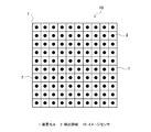
- FIG. 1 It is a top view showing typically composition of an image sensor concerning a 1st embodiment of this indication.
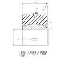
- sectional drawing which shows the structure of the pixel cell 1 shown in FIG.
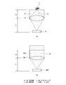
- (A) is a figure which shows the condensing state in the image sensor 10 of this embodiment
- (b) is a figure which shows the condensing state of the conventional image sensor.
- (A) is a figure which shows the focus formation of the micro lens 5
- (b) is a figure which shows a state when it measures with the conventional image sensor.
- It is a figure which shows the suitable conditions of the focal distance f of the micro lens It is a figure which shows typically the state at the time of the measurement of the image sensor 10 shown in FIG.
- First embodiment an example of an image sensor in which a sample is fixed only at the center of a pixel
- Second Embodiment Example of an image sensor in which a light shielding mask is provided in a portion other than the detection region
- Third Embodiment Example of inspection apparatus equipped with an image sensor
- FIG. 1 is a plan view schematically showing the configuration of the image sensor of this embodiment
- FIG. 2 is a cross-sectional view showing the configuration of the pixel cell 1.
- a plurality of microlenses 5 are disposed on a photoelectric conversion unit 3 in which a plurality of light receiving elements constituting the pixel cell 1 are arranged in a matrix. Is arranged.
- An insulating layer 6 is formed so as to cover each microlens 5, and a detection region 2 is provided for each pixel cell 1 on the insulating layer 6.
- the photoelectric conversion unit 3 is a part that detects an optical phenomenon such as a light emission process in the sample 11 by each light receiving element and outputs it as an electrical signal.
- each light receiving element is constituted by a PN junction.
- the size a of each pixel cell 1 of the photoelectric conversion unit 3 is not particularly limited, but may be 0.2 to 10 ⁇ m square, for example.
- the thickness t of the photoelectric conversion unit 3 is not particularly limited, but can be about 1 to 10 ⁇ m as in the case of a conventional image sensor.
- the microlens 5 collects light toward the light receiving unit 4 of each light receiving element disposed in the photoelectric conversion unit 3, and is disposed in the region immediately above the light receiving element for each pixel cell 1.
- one microlens may be provided for one light receiving element, but one microlens may be configured to correspond to a plurality of light receiving elements.
- the shape of the microlens 5 is not particularly limited, and various shapes such as a plano-convex lens and a biconvex lens can be applied.
- the array system is not particularly limited, and is appropriately selected. Can do.
- FIG. 3A is a view showing a light collection state in the image sensor 10 of the present embodiment
- FIG. 3B is a view showing a light collection state of a conventional image sensor
- FIG. 4A is a diagram showing the focus formation of the microlens 5
- FIG. 4B is a diagram showing a state when measured by a conventional image sensor.
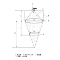
- FIG. 5 is a diagram showing a preferable condition for the focal length f of the microlens 5.
- the components between the light receiving unit 4 and the microlens 5 are omitted and the microlens 5 is described in a biconvex shape for easy viewing.
- a conventional image sensor usually has a structure for condensing parallel light on a light receiving surface. Therefore, when the distance of the refractive index to the light receiving portion 104 is a light receiving surface from the microlens 105 n 1, the lens 105 to the imaging surface set to L 1, the focal length f of the microlens 105, f ⁇ L It is designed to be 1 ⁇ n 1 . For this reason, as shown in FIG. 4B, in the case of the conventional image sensor structure, even if the sample 11 is fixed at the center of the pixel, the distance L 1 from the microlens 105 to the imaging plane is negative. Value, resulting in a system that does not collect light.
- the image sensor 10 of the present embodiment responds by collimating or converging at least light beams emitted from the detection region 2 and being condensed.
- the focal point of the microlens 5 is formed so as to be within the light receiving unit 4. Specifically, the thickness of the insulating layer 6, the distance from the microlens 5 to the light receiving unit 4, the light receiving element and the light receiving unit 4 so that the focal length f of the microlens 5 satisfies f ⁇ L 2 ⁇ n 2. Adjust the size.
- n 2 is the refractive index of the insulating layer 6
- L 2 is the distance from the sample 11 to the microlens 5.
- the focal length f of the microlens 5 is a condition in which all the light from the detection region 2 is geometrically incident on the light receiving unit 4 as shown in FIG.
- the conditions for all the light velocities emitted from the microlens 5 having the aperture S 2 to enter the light receiving unit 4 having the aperture S 1 are as follows. Geometrically, it is expressed by the following mathematical formula (1).
- L 1 in the following equation (1) is the distance from the microlens 5 to the light receiving unit 4
- L 3 is the distance from the microlens 5 to the focal point.
- the focal length f of the microlens 5 is set so as to satisfy the following formula (3). That's fine.
- n 1 in the following mathematical formula (3) is the refractive index from the microlens 5 to the light receiving portion 4, and n 2 is the refractive index of the insulating layer 6.
- the focal length f of the microlens 5 satisfies the following formula (4).
- the insulating layer 6 is provided for protection of the light conversion unit 3, electrical insulation and structural support of the light receiving element and its peripheral integrated circuit, surface flattening, and the like. It is made of a material that does not affect the light detection by the light receiving element.
- the insulating layer 6 is a light-transmitting inorganic material such as silicon oxide (SiO 2 ) and silicon nitride (SiN x ), or a high-melting and light-transmitting polymer material such as polyimide. Can be formed.
- the insulating layer 6 may be formed of a material that transmits only light having a wavelength to be detected, such as fluorescence, and absorbs or reflects light that is not to be detected, such as excitation light.
- a color filter that transmits only light having a wavelength to be detected and absorbs light outside the detection target is interposed between the microlens 5 and the light receiving unit 4. It is desirable to provide it.
- the thickness of the insulating layer 6 is not particularly limited as long as the surface can be flattened, but is preferably about 1 to 30 ⁇ m in relation to the focal length f of the lens.
- the detection region 2 is provided on the surface of the insulating layer 6 so as to be separated for each light receiving element. Further, the center of the detection region 2 is located on an extension line of a line connecting the center of the light receiving unit 4 of each light receiving element and the center of the lens 5 disposed immediately above the center.
- the sample 11 is fixed only in the detection region 2, and only light emission in this portion is detected by the light receiving unit 4.
- the ratio of the detection region 2 in the pixel cell 1 can be set as appropriate in accordance with the size of the light receiving surface of the light receiving element, but is preferably about 1 to 70% from the viewpoint of suppressing crosstalk. .
- the method for fixing the sample 11 is not particularly limited.
- the detection region 2 may be subjected to a surface treatment such as a hydrophobic treatment or a hydrophilic treatment, and the sample 11 may be fixed only to that portion.
- a surface treatment such as a hydrophobic treatment or a hydrophilic treatment
- an antibody, an adapter, a gene adsorbing substance, or the like that binds to the sample 11 is fixed in advance in the detection region 2 by various printing methods such as an ink jet method, and the sample 11 is bound to the sample 11 to thereby bind the sample 11. Can also be fixed.
- a method for manufacturing the image sensor 10 configured as described above will be described.
- a photoelectric conversion unit 3 that includes a plurality of light receiving elements and converts incident light into an electrical signal is formed on a semiconductor wafer.
- a plurality of microlenses 5 for condensing light toward the light receiving portion 4 of the light receiving element located immediately below the light receiving elements are formed in the region immediately above each light receiving element, and further made of a light transmissive material.
- An insulating layer 6 is formed.
- the formation method of these photoelectric conversion part 3, the micro lens 5, and the insulating layer 6 is not specifically limited, A well-known method is applicable.
- the detection region 2 where the sample to be detected is fixed is separated from each other, and the center is arranged directly above and above the center of the light receiving portion of each light receiving element. It is formed so as to be located on the extended line of the line connecting the center of the lens.
- the detection region 2 can be subjected to a surface treatment such as a hydrophobic treatment or a hydrophilic treatment, or an antibody, an adapter or a gene adsorbing substance that binds to the sample 11 can be fixed by various printing methods. . Thereby, the sample 11 can be easily fixed only to the detection region 2. Thereafter, the wafer is cut by a known method and separated into individual image sensors 10.
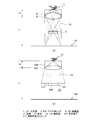
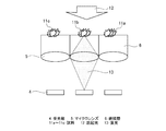
- FIG. 6 is a diagram schematically illustrating a state during measurement of the image sensor 10
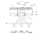
- FIG. 7 is a diagram schematically illustrating a state during measurement when the detection region 2 is not limited to the center of the pixel. .
- the components between the light receiving unit 4 and the microlens 5 are omitted, and the microlens 5 is shown in a biconvex shape for easy viewing.
- the samples 11a to 11c fixed to the detection region 2 are irradiated with excitation light 12.
- excitation light 12 fluorescence corresponding to each of the samples 11a to 11c is generated.
- the fluorescence 13 generated by the excitation light 12 enters the insulating layer 6, is condensed by the microlens 5, and enters the light receiving unit 4 of the light receiving element.
- the center of the detection region 2 is located on an extension line of a line (optical axis) connecting the center of the microlens 5 and the center of the light receiving unit 4 and only in the vicinity thereof. Luminescence occurs. Thereby, the fluorescence 13 emitted from the sample 11b can be efficiently condensed by the microlens 5, and the detection sensitivity is improved.
- the image sensor 10 can also prevent crosstalk in which fluorescence emitted from the other samples 11 a and 11 c enters the other light receiving unit 4.
- the sample 11 is fixed only in the detection region 2 that is located on the extension line of the optical axis of the microlens 5 and is spaced apart for each light receiving element. Therefore, the light collection efficiency can be increased and the propagation of stray light to adjacent pixels can be prevented.
- FIG. 8 is a cross-sectional view showing the configuration of the pixel cell of the image sensor of this embodiment.
- the same components as those of the pixel cell 1 of the image sensor according to the first embodiment shown in FIG. 2 are denoted by the same reference numerals, and detailed description thereof is omitted.
- a light shielding mask 22 that shields light is formed in a portion other than the detection region 2 on the surface of the insulating layer 6.
- the light shielding mask 22 is not particularly limited as long as it absorbs and / or reflects light such as the excitation light 12 or the fluorescence 13 emitted from the sample 11, and the material thereof is not particularly limited. It can be formed of a thin film and a photosensitive resin. Further, the formation method is not particularly limited, and a known method such as dry etching or photolithography can be applied.
- nuclei are randomly formed at such a density that the nuclei that cause the light emission process enter each non-light-shielding portion (detection region 2) of each pixel cell 21 approximately one by one. be able to.
- the sample 11 may be fixed to a part other than the detection region 2. For this reason, for example, printing with rougher accuracy may be performed on the light shielding mask 22 to fix the sample 11 and the antibody, adapter, or gene adsorbing substance that binds to the sample 11 to the surface of the pixel cell 21.
- the light shielding mask 22 is formed in a portion other than the detection region 2, even if the sample 11 is fixed over the entire surface of the pixel cell 21, the adjacent pixel Propagation of stray light to can be prevented.
- the configuration and effects of the image sensor of this embodiment other than those described above are the same as those of the first embodiment described above.
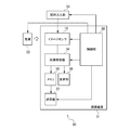
- FIG. 9 is a block diagram showing the configuration of the inspection apparatus of the present embodiment.
- the inspection apparatus 30 according to the present embodiment includes the image sensor 10 according to the first embodiment described above.
- a light source is applied to the sample 11 injected from the sample injection unit 33.
- the light emitted from 32 is irradiated and the light emission process is detected.
- the image processing device 34 of the inspection device 30 includes an image processing unit 34 that processes detection signals, a memory 35 that stores processed data, a display unit 36 that displays data, and data in the memory 35.
- a transmission unit 37 for transmission is provided.
- the imaging device 31 is provided with a control unit 38 that controls the image sensor 10, the image processing unit 34, the transmission unit 37, the light source 32, and the sample injection unit 33.
- the image sensor 10 in which the propagation of stray light to the adjacent pixels is reduced is mounted, the light emission process of the sample can be detected with high accuracy.
- the case where the image sensor 10 is mounted has been described as an example.
- the present disclosure is not limited thereto, and even when the image sensor according to the second embodiment is mounted, Similar effects can be obtained.
- a light source converter that includes a plurality of light receiving elements and converts incident light into an electrical signal; A plurality of lenses that are arranged in a region immediately above each light receiving element and collect light toward a light receiving portion of the light receiving element located immediately below the light receiving element; An insulating layer formed on the lens and made of a light transmitting material; Each of the light receiving elements is provided on the surface of the insulating layer so as to be separated from each other, and the center thereof is located on an extension of a line connecting the center of the light receiving portion of each light receiving element and the center of the lens disposed immediately above the center.
- a detection area Have An image sensor in which a sample to be detected is fixed at least in the detection region.
- Image sensor (3) The image sensor according to (1) or (2), wherein a sample to be detected is fixed only in the detection region. (4) The image sensor according to (3), wherein the detection region is subjected to a surface treatment. (5) The image sensor according to (3), wherein an antibody, an adapter, or a gene adsorbing substance that binds to the sample is fixed in the detection region.
- Forming a photoelectric conversion unit that includes a plurality of light receiving elements on a semiconductor wafer and converts incident light into an electrical signal; Forming a plurality of lenses for condensing light in a region immediately above each light receiving element toward a light receiving portion of the light receiving element located immediately below the light receiving element; Forming an insulating layer made of a light transmissive material on the lens; A detection region where a sample to be detected is fixed for each light receiving element is separated from each other on the surface of the insulating layer, and the center of the light receiving portion of each light receiving element and the center of the lens disposed immediately above the center.
- a step of forming the wire so as to be positioned on the extended line of the wire A method for manufacturing an image sensor.
Landscapes
- Health & Medical Sciences (AREA)
- Physics & Mathematics (AREA)
- General Physics & Mathematics (AREA)
- Immunology (AREA)
- Chemical & Material Sciences (AREA)
- Analytical Chemistry (AREA)
- Biochemistry (AREA)
- General Health & Medical Sciences (AREA)
- Nuclear Medicine, Radiotherapy & Molecular Imaging (AREA)
- Life Sciences & Earth Sciences (AREA)
- Pathology (AREA)
- Engineering & Computer Science (AREA)
- Multimedia (AREA)
- Signal Processing (AREA)
- Investigating, Analyzing Materials By Fluorescence Or Luminescence (AREA)
- Solid State Image Pick-Up Elements (AREA)
- Electromagnetism (AREA)
- Transforming Light Signals Into Electric Signals (AREA)
Abstract
【課題】集光効率が高く、かつ画素間のクロストークが少ないイメージセンサ及びその製造方法並びに検査装置を提供する。 【解決手段】複数の受光素子を備え、入射した光を電気信号に変換する光源変換部と、各受光素子の直上域に配置され、その直下に位置する受光素子に向けて光を集光する複数のレンズと、このレンズ上に形成され、光透過材料からなる絶縁層とを備えるイメージセンサにおいて、絶縁層の表面に、受光素子毎にそれぞれ離間して形成され、その中心が、各受光素子の受光部の中心とその直上に配置されたレンズの中心とを結んだ線の延長線上に位置する検出領域を設ける。そして、検出対象の試料を、少なくともこの検出領域に固定する。
Description
本技術は、集光構造を備えるイメージセンサ及びその製造方法並びに検査装置に関する。より詳しくは、試料の発光過程を検出するイメージセンサ及びその製造方法並びに検査装置に関する。
生命科学領域には、微小な発光過程を、多数の試料について同時並行的に検出する分析手法がある。例えば、溶液中に含まれるタンパク質を同定したい場合には、従来、ELISA法(Enzyme Linked Immuno Sorbent Assay:酵素免疫測定法)などが利用されている。ELISA法は、多数の抗体を配列・固定した基板を、測定対象のタンパク質を含有する溶液に浸漬した後、更に蛍光修飾した抗体にさらし、これを励起光に暴露して顕微鏡などで観察する測定法であり、蛍光の位置からどの抗体が反応したかを判別することができる。
一方、蛍光をはじめとして発光過程で生じる光の多くは、周囲の空間に等方的に放射される。このため、前述したELISA法などのように、発光過程の観察に顕微鏡を用いる方法は、検出効率が顕微鏡の集光効率によって制限され、良好な結果が得られないという問題がある。
この発光過程における検出効率を向上させる方法としては、受光素子を発光源(試料)近傍に設置することが考えられる。例えば、検出対象の発光過程が、十分に小さい空間で生じる現象であれば、CMOS(Complementary Metal Oxide Semiconductor:相補性金属酸化膜半導体)やCCD(Charge Coupled Device:電荷結合素子)イメージセンサを用いることができる。
その場合、これらのイメージセンサの単位ピクセルに1つの発光過程を対応させる形態で、光検出系を構成することにより、同時並行的に100万単位の発光過程を、時系列で記録及び解析することができる。また、イメージセンサの表面近傍でこれらの発光過程が出現するような構成とすることで、多数の試料について同時並行的発光過程を、小型の検出系で測定することが可能となる。
このような理由から、従来、細胞などの生体組織を測定するためのイメージセンサが提案されている(例えば、特許文献1,2参照)。例えば、特許文献1に記載のイメージセンサでは、検出精度を向上させるために、各画素セルのフォトダイオード上面に、励起光の波長域を遮断すると共に蛍光の波長域を透過する光学フィルター層を設けている。
一方、特許文献2に記載のイメージセンサは、受光面上に反射防止膜を形成することにより、受光面における透過率を向上させて、検出感度の向上を図っている。また、特許文献2に記載のイメージセンサでは、一本鎖プローブDNAなどの生体高分子が多数集まったスポットを、反射防止膜上にマトリクス状に形成し、このスポットに特定のサンプルが結合するようにしている。
しかしながら、前述した従来のイメージセンサには、隣接する画素間でクロストークが生じるという問題点がある。例えば、センサ表面近傍で発光過程が生じた場合、前述したように試料から発せられた光は全方向に均等に放射されるため、直下の画素のみならず、その近傍の画素にも影響を与える。このため、従来のイメージセンサでは、ピクセル毎に独立して発光過程を検出することができず、必然的に検出できる発光過程の数が限られてしまう。
この画素間のクロストークを低減する方法としては、イメージセンサの各画素の間に遮光壁を設けることが考えられるが、その場合、製造工程が複雑になるため、従来のイメージセンサでは、完全な遮光壁は形成されていないのが現状である。
そこで、本開示は、集光効率が高く、かつ画素間のクロストークが少ないイメージセンサ及びその製造方法並びに検査装置を提供することを主目的とする。
本開示のイメージセンサは、複数の受光素子を備え、入射した光を電気信号に変換する光源変換部と、各受光素子の直上域に配置され、その直下に位置する受光素子の受光部に向けて光を集光する複数のレンズと、前記レンズ上に形成され、光透過材料からなる絶縁層と、前記絶縁層の表面に受光素子毎にそれぞれ離間して設けられ、その中心が、各受光素子の受光部の中心とその直上に配置されたレンズの中心とを結んだ線の延長線上に位置する検出領域と、を有し、検出対象の試料は少なくとも前記検出領域に固定されるものである。
このイメージセンサでは、絶縁層の屈折率をn、試料からレンズまでの距離をLとしたとき、前記レンズの焦点距離fを、試料とレンズ間の光路長(=n×L)よりも短くしてもよい。
また、前記検出領域にのみ検出対象の試料を固定することができる。
その場合、前記検出領域には、表面処理が施されていてもよく、又は、前記試料と結合する抗体、アダプター若しくは遺伝子吸着物質が固定されていてもよい。
更に、前記絶縁層の表面には、前記検出領域以外の部分に、遮光マスクが形成されていてもよい。
更にまた、前記絶縁層は、シリコンオキサイドにより形成することができる。
このイメージセンサでは、絶縁層の屈折率をn、試料からレンズまでの距離をLとしたとき、前記レンズの焦点距離fを、試料とレンズ間の光路長(=n×L)よりも短くしてもよい。
また、前記検出領域にのみ検出対象の試料を固定することができる。
その場合、前記検出領域には、表面処理が施されていてもよく、又は、前記試料と結合する抗体、アダプター若しくは遺伝子吸着物質が固定されていてもよい。
更に、前記絶縁層の表面には、前記検出領域以外の部分に、遮光マスクが形成されていてもよい。
更にまた、前記絶縁層は、シリコンオキサイドにより形成することができる。
本開示のイメージセンサの製造方法は、半導体ウエハに、複数の受光素子を備え、入射した光を電気信号に変換する光電変換部を形成する工程と、各受光素子の直上域に、その直下に位置する受光素子の受光部に向けて光を集光する複数のレンズを形成する工程と、前記レンズ上に、光透過性材料からなる絶縁層を形成する工程と、前記絶縁層の表面に、受光素子毎に、検出対象の試料が固定される検出領域を、相互に離間し、かつ中心が各受光素子の受光部の中心とその直上に配置されたレンズの中心とを結んだ線の延長線上に位置するように形成する工程と、を有する。
本開示の検査装置は、前述したイメージセンサが搭載されたものである。
本開示によれば、絶縁層の表面の各受光素子の中心部の直上域に検出領域が設けられているため、集光効率が向上すると共に、画素間のクロストークを低減することができる。
以下、本開示を実施するための形態について、添付の図面を参照して詳細に説明する。
なお、本開示は、以下に示す各実施形態に限定されるものではない。また、説明は、以下の順序で行う。
1.第1の実施の形態
(画素中心部にのみ試料が固定されるイメージセンサの例)
2.第2の実施の形態
(検出領域以外の部分に遮光マスクが設けられたイメージセンサの例)
3.第3の実施の形態
(イメージセンサを搭載した検査装置の例)
なお、本開示は、以下に示す各実施形態に限定されるものではない。また、説明は、以下の順序で行う。
1.第1の実施の形態
(画素中心部にのみ試料が固定されるイメージセンサの例)
2.第2の実施の形態
(検出領域以外の部分に遮光マスクが設けられたイメージセンサの例)
3.第3の実施の形態
(イメージセンサを搭載した検査装置の例)
<1.第1の実施の形態>
先ず、本開示の第1の実施形態に係るイメージセンサについて説明する。図1は本実施形態のイメージセンサの構成を模式的に示す平面図であり、図2はその画素セル1の構成を示す断面図である。
先ず、本開示の第1の実施形態に係るイメージセンサについて説明する。図1は本実施形態のイメージセンサの構成を模式的に示す平面図であり、図2はその画素セル1の構成を示す断面図である。
[全体構成]
図1及び図2に示すように、本実施形態のイメージセンサ10では、画素セル1を構成する複数の受光素子がマトリクス状に配設された光電変換部3の上に、複数のマイクロレンズ5が配置されている。そして、各マイクロレンズ5を覆うように絶縁層6が形成されており、絶縁層6上には、画素セル1ごとに検出領域2が設けられている。
図1及び図2に示すように、本実施形態のイメージセンサ10では、画素セル1を構成する複数の受光素子がマトリクス状に配設された光電変換部3の上に、複数のマイクロレンズ5が配置されている。そして、各マイクロレンズ5を覆うように絶縁層6が形成されており、絶縁層6上には、画素セル1ごとに検出領域2が設けられている。
[光電変換部3]
光電変換部3は、各受光素子により、試料11における発光過程などの光現象を検出して、電気信号として出力する部分である。例えば、CCDやCMOSなどの固体撮像素子を用いた場合、各受光素子はPN接合により構成される。また、光電変換部3の各画素セル1のサイズaは、特に限定されるものではないが、例えば0.2~10μm角とすることができる。更に、光電変換部3の厚さtも、特に限定されるものではないが、従来のイメージセンサと同様に1~10μm程度とすることができる。
光電変換部3は、各受光素子により、試料11における発光過程などの光現象を検出して、電気信号として出力する部分である。例えば、CCDやCMOSなどの固体撮像素子を用いた場合、各受光素子はPN接合により構成される。また、光電変換部3の各画素セル1のサイズaは、特に限定されるものではないが、例えば0.2~10μm角とすることができる。更に、光電変換部3の厚さtも、特に限定されるものではないが、従来のイメージセンサと同様に1~10μm程度とすることができる。
[マイクロレンズ5]
マイクロレンズ5は、光電変換部3に配設された各受光素子の受光部4に向けて光を集光するものであり、画素セル1ごとに受光素子の直上域に配置されている。本実施形態のイメージセンサ10においては、1つの受光素子に対して1つのマイクロレンズが設けられていてもよいが、1つのマイクロレンズが複数の受光素子に対応する構成としてもよい。また、マイクロレンズ5の形状は、特に限定されるものではなく、平凸レンズや両凸レンズなど各種形状のものを適用することができ、そのアレイ方式も特に限定されるものではなく、適宜選択することができる。
マイクロレンズ5は、光電変換部3に配設された各受光素子の受光部4に向けて光を集光するものであり、画素セル1ごとに受光素子の直上域に配置されている。本実施形態のイメージセンサ10においては、1つの受光素子に対して1つのマイクロレンズが設けられていてもよいが、1つのマイクロレンズが複数の受光素子に対応する構成としてもよい。また、マイクロレンズ5の形状は、特に限定されるものではなく、平凸レンズや両凸レンズなど各種形状のものを適用することができ、そのアレイ方式も特に限定されるものではなく、適宜選択することができる。
図3(a)は本実施形態のイメージセンサ10における集光状態を示す図であり、図3(b)は従来のイメージセンサの集光状態を示す図である。また、図4(a)はマイクロレンズ5の焦点形成を示す図である、図4(b)は従来のイメージセンサで測定したときの状態を示す図である。更に、図5はマイクロレンズ5の焦点距離fの好適な条件を示す図である。更に、なお、図3~図5においては、図を見やすくするために、受光部4とマイクロレンズ5との間の構成要素は省略し、マイクロレンズ5を両凸形状で記載している。
図3(b)に示すように、従来のイメージセンサでは、通常、平行光を受光面に集光する構造をとっている。このため、マイクロレンズ105から受光面である受光部104までの屈折率をn1、レンズ105から結像面までの距離をL1としたとき、マイクロレンズ105の焦点距離fは、f≧L1×n1となるように設計されている。このため、図4(b)に示すように、従来のイメージセンサ構造の場合、仮に、画素中央部に試料11を固定したとしても、マイクロレンズ105から結像面までの距離L1は負の値となり、集光しない系となってしまう。
一方、図3(a)及び図4(b)に示すように、本実施形態のイメージセンサ10では、検出領域2から発せられ、少なくとも集光途中にある光束を並行又は収束させて、対応する受光部4内に収まるように、マイクロレンズ5の焦点を形成する。具体的には、マイクロレンズ5の焦点距離fが、f<L2×n2となるように、絶縁層6の厚さ、マイクロレンズ5から受光部4までの距離及び受光素子や受光部4の大きさなどを調整する。ここで、n2は絶縁層6の屈折率、L2は試料11からマイクロレンズ5までの距離である。
更に、マイクロレンズ5の焦点距離fは、図5に示すように検出領域2からの光が幾何学的に全て受光部4に入射する条件であることが好ましい。具体的には、検出領域2がマイクロレンズ5の光軸近傍のみに存在する場合は、口径S2のマイクロレンズ5から出射した光速が、全て、口径S1の受光部4に入射する条件は、幾何学的には、下記数式(1)で表される。ここで、下記数式(1)におけるL1はマイクロレンズ5から受光部4までの距離であり、L3はマイクロレンズ5から焦点までの距離である。

上記数式(1)をL3について解くと、下記数式(2)となる。

そして、検出領域2からの光を、上記数式(2)で表されるL3よりも手前で合焦させるためには、マイクロレンズ5の焦点距離fが下記数式(3)を満たすようにすればよい。ここで、下記数式(3)におけるn1はマイクロレンズ5から受光部4までの屈折率、n2は絶縁層6の屈折率である。

なお、マイクロレンズ5の焦点距離fは、下記数式(4)を満たすことが理想である。

[絶縁層6]
絶縁層6は、光変換部3の保護、受光素子及びその周辺集積回路の電気的絶縁並びに構造的支持、表面の平坦化などのために設けられており、光を透過し、かつ試料11や受光素子での光検出に影響しない材料で形成されている。具体的には、絶縁層6は、例えば酸化シリコン(SiO2)及び窒化シリコン(SiNx)などの光透過性がある無機材料、ポリイミドなどの高融点でかつ光透過性がある高分子材料で形成することができる。
絶縁層6は、光変換部3の保護、受光素子及びその周辺集積回路の電気的絶縁並びに構造的支持、表面の平坦化などのために設けられており、光を透過し、かつ試料11や受光素子での光検出に影響しない材料で形成されている。具体的には、絶縁層6は、例えば酸化シリコン(SiO2)及び窒化シリコン(SiNx)などの光透過性がある無機材料、ポリイミドなどの高融点でかつ光透過性がある高分子材料で形成することができる。
また、蛍光などの検出対象の波長の光のみを透過し、励起光など検出対象外の光を吸収又は反射する材料で形成してもよい。更に、絶縁層6が透明材料で形成されている場合は、マイクロレンズ5と受光部4との間に、検出対象の波長の光のみを透過し、検出対象外の光を吸収するカラーフィルターを設けることが望ましい。なお、絶縁層6の厚さは、特に限定されるものではなく、表面を平坦化できる程度であればよいが、レンズの焦点距離fとの関係から、1~30μm程度が好適である。
[検出領域2]
検出領域2は、絶縁層6の表面に、受光素子ごとにそれぞれ離間して設けられている。また、検出領域2の中心は、各受光素子の受光部4の中心とその直上に配置されたレンズ5の中心とを結んだ線の延長線上に位置している。そして、本実施形態のイメージセンサ10においては、検出領域2にのみ試料11が固定され、この部分での発光のみが受光部4において検出される。ここで、画素セル1における検出領域2の割合は、受光素子の受光面の大きさなどに応じて適宜設定することができるが、クロストーク抑制の観点から、1~70%程度が好適である。
検出領域2は、絶縁層6の表面に、受光素子ごとにそれぞれ離間して設けられている。また、検出領域2の中心は、各受光素子の受光部4の中心とその直上に配置されたレンズ5の中心とを結んだ線の延長線上に位置している。そして、本実施形態のイメージセンサ10においては、検出領域2にのみ試料11が固定され、この部分での発光のみが受光部4において検出される。ここで、画素セル1における検出領域2の割合は、受光素子の受光面の大きさなどに応じて適宜設定することができるが、クロストーク抑制の観点から、1~70%程度が好適である。
試料11を固定する方法は、特に限定されるものではないが、例えば、検出領域2に疎水処理又は親水処理などの表面処理を施し、その部分にのみ、試料11が固定されるようにしてもよい。また、予め、インクジェット法などの各種印刷方法などにより、検出領域2に、試料11と結合する抗体、アダプター又は遺伝子吸着物質などを固定しておき、これらに試料11を結合させることにより、試料11を固定することもできる。
[製造方法]
次に、前述の如く構成されるイメージセンサ10の製造方法について説明する。本実施形態のイメージセンサ10を製造する場合は、先ず、半導体ウエハに、複数の受光素子を備え、入射した光を電気信号に変換する光電変換部3を形成する。次に、各受光素子の直上域に、その直下に位置する受光素子の受光部4に向けて光を集光する複数のマイクロレンズ5を形成し、更に、その上に光透過性材料からなる絶縁層6を形成する。これら光電変換部3、マイクロレンズ5及び絶縁層6の形成方法は、特に限定されるものではなく、公知の方法を適用することができる。
次に、前述の如く構成されるイメージセンサ10の製造方法について説明する。本実施形態のイメージセンサ10を製造する場合は、先ず、半導体ウエハに、複数の受光素子を備え、入射した光を電気信号に変換する光電変換部3を形成する。次に、各受光素子の直上域に、その直下に位置する受光素子の受光部4に向けて光を集光する複数のマイクロレンズ5を形成し、更に、その上に光透過性材料からなる絶縁層6を形成する。これら光電変換部3、マイクロレンズ5及び絶縁層6の形成方法は、特に限定されるものではなく、公知の方法を適用することができる。
次に、絶縁層6の表面に、受光素子毎に、検出対象の試料が固定される検出領域2を、相互に離間し、かつ中心が各受光素子の受光部の中心とその直上に配置されたレンズの中心とを結んだ線の延長線上に位置するように形成する。その際、例えば、検出領域2に、疎水処理や親水処理などの表面処理を施したり、各種印刷方法などによって、試料11と結合する抗体、アダプター若しくは遺伝子吸着物質などを固定したりすることもできる。これにより、容易に、検出領域2にのみ試料11を固定することができる。その後、公知の方法によりウエハを切断し、個々のイメージセンサ10に分離する。
[動作]
次に、本実施形態のイメージセンサ10の動作について、蛍光色素で修飾された試料の発光過程を測定する場合を例にして説明する。図6はイメージセンサ10の測定時の状態を模式的に示す図であり、図7は検出領域2を画素の中心部に限定しなかった場合の測定時の状態を模式的に示す図である。なお、図6及び図7においては、図を見やすくするために、受光部4とマイクロレンズ5との間の構成要素は省略し、マイクロレンズ5を両凸形状で記載している。
次に、本実施形態のイメージセンサ10の動作について、蛍光色素で修飾された試料の発光過程を測定する場合を例にして説明する。図6はイメージセンサ10の測定時の状態を模式的に示す図であり、図7は検出領域2を画素の中心部に限定しなかった場合の測定時の状態を模式的に示す図である。なお、図6及び図7においては、図を見やすくするために、受光部4とマイクロレンズ5との間の構成要素は省略し、マイクロレンズ5を両凸形状で記載している。
図6に示すように、本実施形態のイメージセンサ10では、検出領域2に固定された試料11a~11cに励起光12を照射する。これにより、各試料11a~11cに応じた蛍光が発生する。そして、例えば、試料11bの場合、励起光12により生じた蛍光13は、絶縁層6に入射し、マイクロレンズ5で集光され、受光素子の受光部4に入射する。
このとき、本実施形態のイメージセンサ10では、検出領域2の中心が、マイクロレンズ5の中心と受光部4の中心を結ぶ線(光軸)の延長線上に位置しており、その近傍でのみ発光が生じる。これにより、試料11bから発せられた蛍光13を、マイクロレンズ5で効率的に集光することができ、検出感度が向上する。また、イメージセンサ10は、他の試料11a,11cから発せられた蛍光が他の受光部4に入射するクロストークも防止できる。
これに対して、図7に示す従来のイメージセンサでは、各画素セル1の全面に試料11a~11cが固定されているため、例えば、励起光12の照射により試料11bから発せられた蛍光13は、同一画素セル1内の受光部4に集光されると共に、それ以外にも隣接する他の受光部4にも入射する。即ち、隣接する画素間で、クロストークが生じる。
以上詳述したように、本実施形態のイメージセンサ10では、その中心がマイクロレンズ5の光軸の延長線上位置し、受光素子毎に離間して設けられた検出領域2にのみ試料11が固定されるため、集光効率を高めることができると共に、隣接画素への迷光の伝搬を防止することができる。
<2.第2の実施の形態>
次に、本開示の第2の実施形態に係るイメージセンサについて説明する。図8は本実施形態のイメージセンサの画素セルの構成を示す断面図である。なお、図8においては、図2に示す第1の実施形態のイメージセンサの画素セル1の構成要素と同じものには同じ符号を付し、その詳細な説明は省略する。
次に、本開示の第2の実施形態に係るイメージセンサについて説明する。図8は本実施形態のイメージセンサの画素セルの構成を示す断面図である。なお、図8においては、図2に示す第1の実施形態のイメージセンサの画素セル1の構成要素と同じものには同じ符号を付し、その詳細な説明は省略する。
[全体構成]
図8に示すように、本実施形態のイメージセンサにおいては、絶縁層6の表面の検出領域2以外の部分に、光を遮光する遮光マスク22が形成されている。
図8に示すように、本実施形態のイメージセンサにおいては、絶縁層6の表面の検出領域2以外の部分に、光を遮光する遮光マスク22が形成されている。
[遮光マスク22]
遮光マスク22は、励起光12や試料11から発せられる蛍光13などの光を吸収及び/又は反射するものであればよく、その材質は特に限定されるものではないが、例えばアルミニウム薄膜、酸化クロム薄膜及び感光性樹脂などにより形成することができる。また、その形成方法も、特に限定されるものではなく、ドライエッチングや光リソグラフィーなどの公知の方法を適用することができる。
遮光マスク22は、励起光12や試料11から発せられる蛍光13などの光を吸収及び/又は反射するものであればよく、その材質は特に限定されるものではないが、例えばアルミニウム薄膜、酸化クロム薄膜及び感光性樹脂などにより形成することができる。また、その形成方法も、特に限定されるものではなく、ドライエッチングや光リソグラフィーなどの公知の方法を適用することができる。
[動作]
本実施形態のイメージセンサは、例えば、発光過程の要因となる核が、各画素セル21の非遮光部(検出領域2)に、およそ1つずつ入る程度の密度でランダムに核の形成を行うことができる。また、本実施形態のイメージセンサでは、検出領域2以外の部分にも試料11が固定されていてもよい。このため、例えば、遮光マスク22の上から、より荒い精度で印刷など行い、試料11や、試料11と結合する抗体、アダプター又は遺伝子吸着物質を画素セル21の表面に固定してもよい。
本実施形態のイメージセンサは、例えば、発光過程の要因となる核が、各画素セル21の非遮光部(検出領域2)に、およそ1つずつ入る程度の密度でランダムに核の形成を行うことができる。また、本実施形態のイメージセンサでは、検出領域2以外の部分にも試料11が固定されていてもよい。このため、例えば、遮光マスク22の上から、より荒い精度で印刷など行い、試料11や、試料11と結合する抗体、アダプター又は遺伝子吸着物質を画素セル21の表面に固定してもよい。
以上詳述したように、本実施形態のイメージセンサでは、検出領域2以外の部分に遮光マスク22が形成されているため、画素セル21の表面全域に試料11が固定されていても、隣接画素への迷光の伝搬を防止することができる。なお、本実施形態のイメージセンサにおける上記以外の構成及び効果は、前述した第1の実施形態と同様である。
<2.第3の実施の形態>
次に、本開示の第3の実施形態に係る検査装置について説明する。図9は本実施形態の検査装置の構成を示すブロック図である。図9に示すように、本実施形態の検査装置30は、前述した第1の実施形態のイメージセンサ10が搭載されたものであり、例えば、試料注入部33から注入された試料11に、光源32から出射された光を照射し、その発光過程を検出するものである。
次に、本開示の第3の実施形態に係る検査装置について説明する。図9は本実施形態の検査装置の構成を示すブロック図である。図9に示すように、本実施形態の検査装置30は、前述した第1の実施形態のイメージセンサ10が搭載されたものであり、例えば、試料注入部33から注入された試料11に、光源32から出射された光を照射し、その発光過程を検出するものである。
この検査装置30の撮像装置31には、イメージセンサ10の他に、検出信号を処理する画像処理部34、処理されたデータを記憶するメモリ35や表示する表示部36、メモリ35内のデータを送信する送信部37が設けられている。また、撮像装置31には、イメージセンサ10、画像処理部34、送信部37、光源32及び試料注入部33を制御する制御部38が設けられている。
本実施形態の検査装置30では、隣接画素への迷光の伝搬が低減されたイメージセンサ10を搭載しているため、精度良く試料の発光過程を検出することができる。なお、本実施形態において、イメージセンサ10が搭載されている場合を例にして説明したが、本開示はこれに限定されるものではなく、第2の実施形態のイメージセンサを搭載した場合でも、同様の効果が得られる。
また、本開示は、以下のような構成をとることもできる。
(1)
複数の受光素子を備え、入射した光を電気信号に変換する光源変換部と、
各受光素子の直上域に配置され、その直下に位置する受光素子の受光部に向けて光を集光する複数のレンズと、
前記レンズ上に形成され、光透過材料からなる絶縁層と、
前記絶縁層の表面に受光素子毎にそれぞれ離間して設けられ、その中心が、各受光素子の受光部の中心とその直上に配置されたレンズの中心とを結んだ線の延長線上に位置する検出領域と、
を有し、
検出対象の試料は少なくとも前記検出領域に固定されるイメージセンサ。
(2)
絶縁層の屈折率をn、試料からレンズまでの距離をLとしたとき、前記レンズの焦点距離fが、試料とレンズ間の光路長(=n×L)よりも短い(1)に記載のイメージセンサ。
(3)
前記検出領域にのみ検出対象の試料が固定される(1)又は(2)に記載のイメージセンサ。
(4)
前記検出領域には、表面処理が施されている(3)に記載のイメージセンサ。
(5)
前記検出領域には、前記試料と結合する抗体、アダプター又は遺伝子吸着物質が固定されている(3)に記載のイメージセンサ。
(6)
前記絶縁層の表面には、前記検出領域以外の部分に、遮光マスクが形成されている(1)~(5)のいずれかに記載のイメージセンサ。
(7)
前記絶縁層は、シリコンオキサイドにより形成されている(1)~(6)のいずれかに記載のイメージセンサ。
(8)
半導体ウエハに、複数の受光素子を備え、入射した光を電気信号に変換する光電変換部を形成する工程と、
各受光素子の直上域に、その直下に位置する受光素子の受光部に向けて光を集光する複数のレンズを形成する工程と、
前記レンズ上に、光透過性材料からなる絶縁層を形成する工程と、
前記絶縁層の表面に、受光素子毎に、検出対象の試料が固定される検出領域を、相互に離間し、かつ中心が各受光素子の受光部の中心とその直上に配置されたレンズの中心とを結んだ線の延長線上に位置するように形成する工程と、
を有するイメージセンサの製造方法。
(9)
(1)~(7)のいずれかに記載のイメージセンサが搭載された検査装置。
(1)
複数の受光素子を備え、入射した光を電気信号に変換する光源変換部と、
各受光素子の直上域に配置され、その直下に位置する受光素子の受光部に向けて光を集光する複数のレンズと、
前記レンズ上に形成され、光透過材料からなる絶縁層と、
前記絶縁層の表面に受光素子毎にそれぞれ離間して設けられ、その中心が、各受光素子の受光部の中心とその直上に配置されたレンズの中心とを結んだ線の延長線上に位置する検出領域と、
を有し、
検出対象の試料は少なくとも前記検出領域に固定されるイメージセンサ。
(2)
絶縁層の屈折率をn、試料からレンズまでの距離をLとしたとき、前記レンズの焦点距離fが、試料とレンズ間の光路長(=n×L)よりも短い(1)に記載のイメージセンサ。
(3)
前記検出領域にのみ検出対象の試料が固定される(1)又は(2)に記載のイメージセンサ。
(4)
前記検出領域には、表面処理が施されている(3)に記載のイメージセンサ。
(5)
前記検出領域には、前記試料と結合する抗体、アダプター又は遺伝子吸着物質が固定されている(3)に記載のイメージセンサ。
(6)
前記絶縁層の表面には、前記検出領域以外の部分に、遮光マスクが形成されている(1)~(5)のいずれかに記載のイメージセンサ。
(7)
前記絶縁層は、シリコンオキサイドにより形成されている(1)~(6)のいずれかに記載のイメージセンサ。
(8)
半導体ウエハに、複数の受光素子を備え、入射した光を電気信号に変換する光電変換部を形成する工程と、
各受光素子の直上域に、その直下に位置する受光素子の受光部に向けて光を集光する複数のレンズを形成する工程と、
前記レンズ上に、光透過性材料からなる絶縁層を形成する工程と、
前記絶縁層の表面に、受光素子毎に、検出対象の試料が固定される検出領域を、相互に離間し、かつ中心が各受光素子の受光部の中心とその直上に配置されたレンズの中心とを結んだ線の延長線上に位置するように形成する工程と、
を有するイメージセンサの製造方法。
(9)
(1)~(7)のいずれかに記載のイメージセンサが搭載された検査装置。
1、21 画素セル
2 検出領域
3 光電変換部
4、104 受光部
5、105 マイクロレンズ
6 絶縁層
10 イメージセンサ
11、11a~11c 試料
12 励起光
13 蛍光
a 画素セル1のサイズ
t 光電変換部3の厚さ
30 検査装置
31 撮像装置
32 光源
33 試料注入部
34 画像処理部
35 メモリ
36 表示部
37 送信部
38 制御部
2 検出領域
3 光電変換部
4、104 受光部
5、105 マイクロレンズ
6 絶縁層
10 イメージセンサ
11、11a~11c 試料
12 励起光
13 蛍光
a 画素セル1のサイズ
t 光電変換部3の厚さ
30 検査装置
31 撮像装置
32 光源
33 試料注入部
34 画像処理部
35 メモリ
36 表示部
37 送信部
38 制御部
Claims (9)
- 複数の受光素子を備え、入射した光を電気信号に変換する光源変換部と、
各受光素子の直上域に配置され、その直下に位置する受光素子の受光部に向けて光を集光する複数のレンズと、
前記レンズ上に形成され、光透過材料からなる絶縁層と、
前記絶縁層の表面に受光素子毎にそれぞれ離間して設けられ、その中心が、各受光素子の受光部の中心とその直上に配置されたレンズの中心とを結んだ線の延長線上に位置する検出領域と、
を有し、
検出対象の試料は少なくとも前記検出領域に固定されるイメージセンサ。 - 絶縁層の屈折率をn、試料からレンズまでの距離をLとしたとき、前記レンズの焦点距離fが、試料とレンズ間の光路長(=n×L)よりも短い請求項1に記載のイメージセンサ。
- 前記検出領域にのみ検出対象の試料が固定される請求項1に記載のイメージセンサ。
- 前記検出領域には、表面処理が施されている請求項3に記載のイメージセンサ。
- 前記検出領域には、前記試料と結合する抗体、アダプター又は遺伝子吸着物質が固定されている請求項3に記載のイメージセンサ。
- 前記絶縁層の表面には、前記検出領域以外の部分に、遮光マスクが形成されている請求項1に記載のイメージセンサ。
- 前記絶縁層は、シリコンオキサイドにより形成されている請求項1に記載のイメージセンサ。
- 半導体ウエハに、複数の受光素子を備え、入射した光を電気信号に変換する光電変換部を形成する工程と、
各受光素子の直上域に、その直下に位置する受光素子の受光部に向けて光を集光する複数のレンズを形成する工程と、
前記レンズ上に、光透過性材料からなる絶縁層を形成する工程と、
前記絶縁層の表面に、受光素子毎に、検出対象の試料が固定される検出領域を、相互に離間し、かつ中心が各受光素子の受光部の中心とその直上に配置されたレンズの中心とを結んだ線の延長線上に位置するように形成する工程と、
を有するイメージセンサの製造方法。 - 請求項1に記載のイメージセンサが搭載された検査装置。
Priority Applications (3)
| Application Number | Priority Date | Filing Date | Title |
|---|---|---|---|
| US14/127,221 US9324751B2 (en) | 2011-08-24 | 2012-08-01 | Image sensor, production method therefor, and inspection apparatus |
| EP12825220.2A EP2750190B1 (en) | 2011-08-24 | 2012-08-01 | Image sensor, method of manufacturing same, and inspection device |
| CN201280039991.3A CN103733341B (zh) | 2011-08-24 | 2012-08-01 | 图像传感器、其制造方法及检查装置 |
Applications Claiming Priority (2)
| Application Number | Priority Date | Filing Date | Title |
|---|---|---|---|
| JP2011-182131 | 2011-08-24 | ||
| JP2011182131A JP2013045857A (ja) | 2011-08-24 | 2011-08-24 | イメージセンサ及びその製造方法並びに検査装置 |
Publications (1)
| Publication Number | Publication Date |
|---|---|
| WO2013027338A1 true WO2013027338A1 (ja) | 2013-02-28 |
Family
ID=47746112
Family Applications (1)
| Application Number | Title | Priority Date | Filing Date |
|---|---|---|---|
| PCT/JP2012/004883 Ceased WO2013027338A1 (ja) | 2011-08-24 | 2012-08-01 | イメージセンサ及びその製造方法並びに検査装置 |
Country Status (5)
| Country | Link |
|---|---|
| US (1) | US9324751B2 (ja) |
| EP (1) | EP2750190B1 (ja) |
| JP (1) | JP2013045857A (ja) |
| CN (1) | CN103733341B (ja) |
| WO (1) | WO2013027338A1 (ja) |
Cited By (1)
| Publication number | Priority date | Publication date | Assignee | Title |
|---|---|---|---|---|
| KR20160096644A (ko) * | 2013-12-10 | 2016-08-16 | 일루미나, 인코포레이티드 | 생물학적 또는 화학적 분석을 위한 바이오센서들 및 이를 제조하기 위한 방법 |
Families Citing this family (9)
| Publication number | Priority date | Publication date | Assignee | Title |
|---|---|---|---|---|
| WO2015074001A1 (en) | 2013-11-17 | 2015-05-21 | Quantum-Si Incorporated | Optical system and assay chip for probing, detecting and analyzing molecules |
| JP6320870B2 (ja) * | 2014-07-31 | 2018-05-09 | 株式会社東芝 | 顕微撮影装置を用いた観察方法 |
| US20160050376A1 (en) * | 2014-08-18 | 2016-02-18 | Ron Fridental | Image sensor with sub-wavelength resolution |
| SG11201707511UA (en) * | 2015-04-22 | 2017-10-30 | Shenzhen Genorivision Tech Co Ltd | A biosensor |
| JP6462837B2 (ja) * | 2017-12-01 | 2019-01-30 | 株式会社東芝 | 顕微撮影装置を用いた観察方法 |
| JP2020085666A (ja) * | 2018-11-26 | 2020-06-04 | ソニーセミコンダクタソリューションズ株式会社 | 生体由来物質検出用チップ、生体由来物質検出装置及び生体由来物質検出システム |
| JP6692404B2 (ja) * | 2018-12-13 | 2020-05-13 | 株式会社東芝 | 観察システム |
| CN115135988A (zh) * | 2020-02-19 | 2022-09-30 | 索尼半导体解决方案公司 | 生物体导出材料检测芯片、生物体导出材料检测装置及生物体导出材料检测系统 |
| CA3222326A1 (en) * | 2021-08-27 | 2023-03-02 | Illumina, Inc. | Flow cell image sensor arrangement with reduced crosstalk |
Citations (5)
| Publication number | Priority date | Publication date | Assignee | Title |
|---|---|---|---|---|
| JP2003042954A (ja) * | 2001-07-30 | 2003-02-13 | Fuji Photo Film Co Ltd | 生化学解析用データの生成方法および装置 |
| JP2005227155A (ja) | 2004-02-13 | 2005-08-25 | Nara Institute Of Science & Technology | 生体組織測定用イメージセンサ及び該センサを用いた生体組織測定方法 |
| JP2006004991A (ja) * | 2004-06-15 | 2006-01-05 | Casio Comput Co Ltd | 撮像装置及び生体高分子分析チップ |
| JP2006030162A (ja) | 2004-06-18 | 2006-02-02 | Casio Comput Co Ltd | 撮像装置、生体高分子分析チップ及び分析支援装置 |
| JP2009180740A (ja) * | 2009-05-11 | 2009-08-13 | Hitachi High-Technologies Corp | 蛍光分析方法,蛍光分析装置及び画像検出方法 |
Family Cites Families (8)
| Publication number | Priority date | Publication date | Assignee | Title |
|---|---|---|---|---|
| JPS6029717A (ja) * | 1983-07-28 | 1985-02-15 | Canon Inc | 水陸両用カメラの光学系 |
| FR2797053B1 (fr) * | 1999-07-13 | 2001-08-31 | Commissariat Energie Atomique | Support d'analyse a transmission de lumiere de fluorescence |
| US7348587B2 (en) | 2001-06-28 | 2008-03-25 | Fujifilm Corporation | Method for producing biochemical analysis data and apparatus used therefor |
| AU2003290429A1 (en) * | 2002-12-25 | 2004-07-22 | Casio Computer Co., Ltd. | Optical dna sensor, dna reading apparatus, identification method of dna and manufacturing method of optical dna sensor |
| JP3824233B2 (ja) * | 2003-09-01 | 2006-09-20 | セイコーエプソン株式会社 | バイオセンサ及びバイオセンサの製造方法 |
| JP4396407B2 (ja) * | 2004-06-11 | 2010-01-13 | カシオ計算機株式会社 | 生体高分子分析チップ、生体高分子チップの製造方法 |
| JP4431549B2 (ja) * | 2006-05-31 | 2010-03-17 | 株式会社日立ハイテクノロジーズ | 蛍光分析装置 |
| JP2008175712A (ja) * | 2007-01-19 | 2008-07-31 | Casio Comput Co Ltd | 生体高分子分析チップ |
-
2011
- 2011-08-24 JP JP2011182131A patent/JP2013045857A/ja active Pending
-
2012
- 2012-08-01 EP EP12825220.2A patent/EP2750190B1/en not_active Not-in-force
- 2012-08-01 CN CN201280039991.3A patent/CN103733341B/zh not_active Expired - Fee Related
- 2012-08-01 US US14/127,221 patent/US9324751B2/en active Active
- 2012-08-01 WO PCT/JP2012/004883 patent/WO2013027338A1/ja not_active Ceased
Patent Citations (5)
| Publication number | Priority date | Publication date | Assignee | Title |
|---|---|---|---|---|
| JP2003042954A (ja) * | 2001-07-30 | 2003-02-13 | Fuji Photo Film Co Ltd | 生化学解析用データの生成方法および装置 |
| JP2005227155A (ja) | 2004-02-13 | 2005-08-25 | Nara Institute Of Science & Technology | 生体組織測定用イメージセンサ及び該センサを用いた生体組織測定方法 |
| JP2006004991A (ja) * | 2004-06-15 | 2006-01-05 | Casio Comput Co Ltd | 撮像装置及び生体高分子分析チップ |
| JP2006030162A (ja) | 2004-06-18 | 2006-02-02 | Casio Comput Co Ltd | 撮像装置、生体高分子分析チップ及び分析支援装置 |
| JP2009180740A (ja) * | 2009-05-11 | 2009-08-13 | Hitachi High-Technologies Corp | 蛍光分析方法,蛍光分析装置及び画像検出方法 |
Non-Patent Citations (1)
| Title |
|---|
| See also references of EP2750190A4 |
Cited By (15)
| Publication number | Priority date | Publication date | Assignee | Title |
|---|---|---|---|---|
| KR20160096644A (ko) * | 2013-12-10 | 2016-08-16 | 일루미나, 인코포레이티드 | 생물학적 또는 화학적 분석을 위한 바이오센서들 및 이를 제조하기 위한 방법 |
| JP2017504789A (ja) * | 2013-12-10 | 2017-02-09 | イラミーナ インコーポレーテッド | 生物学的または化学的な分析のためのバイオセンサおよびその製造方法 |
| EP3080585A4 (en) * | 2013-12-10 | 2017-08-23 | Illumina, Inc. | Biosensors for biological or chemical analysis and methods of manufacturing the same |
| US10254225B2 (en) | 2013-12-10 | 2019-04-09 | Illumina, Inc. | Biosensors for biological or chemical analysis and methods of manufacturing the same |
| CN110411998A (zh) * | 2013-12-10 | 2019-11-05 | 伊鲁米那股份有限公司 | 用于生物或化学分析的生物传感器及其制造方法 |
| KR102102934B1 (ko) | 2013-12-10 | 2020-04-21 | 일루미나, 인코포레이티드 | 생물학적 또는 화학적 분석을 위한 바이오센서들 및 이를 제조하기 위한 방법 |
| KR20200042023A (ko) * | 2013-12-10 | 2020-04-22 | 일루미나, 인코포레이티드 | 생물학적 또는 화학적 분석을 위한 바이오센서들 및 이를 제조하기 위한 방법 |
| JP2020112560A (ja) * | 2013-12-10 | 2020-07-27 | イラミーナ インコーポレーテッド | 生物学的または化学的な分析のためのバイオセンサおよびその製造方法 |
| KR102271774B1 (ko) | 2013-12-10 | 2021-06-30 | 일루미나, 인코포레이티드 | 생물학적 또는 화학적 분석을 위한 바이오센서들 및 이를 제조하기 위한 방법 |
| US11181478B2 (en) | 2013-12-10 | 2021-11-23 | Illumina, Inc. | Biosensors for biological or chemical analysis and methods of manufacturing the same |
| JP7013503B2 (ja) | 2013-12-10 | 2022-01-31 | イラミーナ インコーポレーテッド | 生物学的または化学的な分析のためのバイオセンサおよびその製造方法 |
| CN110411998B (zh) * | 2013-12-10 | 2022-06-07 | 伊鲁米那股份有限公司 | 用于生物或化学分析的生物传感器及其制造方法 |
| EP4220137A1 (en) * | 2013-12-10 | 2023-08-02 | Illumina, Inc. | Biosensors for biological or chemical analysis and methods of manufacturing the same |
| US11719637B2 (en) | 2013-12-10 | 2023-08-08 | Illumina, Inc. | Biosensors for biological or chemical analysis and methods of manufacturing the same |
| US12140543B2 (en) | 2013-12-10 | 2024-11-12 | Illumina, Inc. | Biosensors for biological or chemical analysis and methods of manufacturing the same |
Also Published As
| Publication number | Publication date |
|---|---|
| US9324751B2 (en) | 2016-04-26 |
| EP2750190A1 (en) | 2014-07-02 |
| US20140118590A1 (en) | 2014-05-01 |
| JP2013045857A (ja) | 2013-03-04 |
| CN103733341B (zh) | 2018-01-26 |
| EP2750190A4 (en) | 2015-04-08 |
| EP2750190B1 (en) | 2019-05-08 |
| CN103733341A (zh) | 2014-04-16 |
Similar Documents
| Publication | Publication Date | Title |
|---|---|---|
| WO2013027338A1 (ja) | イメージセンサ及びその製造方法並びに検査装置 | |
| TWI521205B (zh) | Chemical detectors, biological molecular detection devices and biological molecular detection methods | |
| JP4534352B2 (ja) | 有機分子検出用半導体素子、有機分子検出用半導体装置及びこれを用いた有機分子の測定方法 | |
| CN102110704B (zh) | 图像传感器、制造图像传感器的方法以及传感器设备 | |
| TWI503533B (zh) | Chemical detector, chemical detector module, biological molecular detection device and biological molecular detection method | |
| US8026559B2 (en) | Biosensor devices and method for fabricating the same | |
| EP2221606A2 (en) | Integrated bio-chip and method of fabricating the integrated bio-chip | |
| KR20140027113A (ko) | 도광 픽셀 | |
| US20120200749A1 (en) | Imagers with structures for near field imaging | |
| JP2013045857A5 (ja) | ||
| CN113711368A (zh) | 用于分子检测和感测的高通量分析系统 | |
| TW200844437A (en) | Portable optical detection chip and its manufacturing method thereof | |
| JP5765081B2 (ja) | 撮像素子、電子機器、製造方法、および検査装置 | |
| US20170241997A1 (en) | Chemical sensor, method of producing chemical sensor, and chemical detection apparatus | |
| JP2007207789A (ja) | 固体撮像素子及び該素子を用いた撮像装置 | |
| JP6439810B2 (ja) | バイオチップ、バイオチップユニット、バイオチップ読取装置、及びバイオチップ製造方法 | |
| JP2006030162A (ja) | 撮像装置、生体高分子分析チップ及び分析支援装置 | |
| JP2017037022A (ja) | センシングデバイス | |
| KR101563158B1 (ko) | 집적된 바이오칩 및 이의 제조방법 | |
| CN113686940A (zh) | 用于分子检测和感测的高通量分析系统 | |
| KR101569834B1 (ko) | 집적된 바이오칩 및 이의 제조방법 |
Legal Events
| Date | Code | Title | Description |
|---|---|---|---|
| 121 | Ep: the epo has been informed by wipo that ep was designated in this application |
Ref document number: 12825220 Country of ref document: EP Kind code of ref document: A1 |
|
| WWE | Wipo information: entry into national phase |
Ref document number: 14127221 Country of ref document: US |
|
| NENP | Non-entry into the national phase |
Ref country code: DE |