WO2013027819A1 - 半導体モジュール - Google Patents
半導体モジュール Download PDFInfo
- Publication number
- WO2013027819A1 WO2013027819A1 PCT/JP2012/071398 JP2012071398W WO2013027819A1 WO 2013027819 A1 WO2013027819 A1 WO 2013027819A1 JP 2012071398 W JP2012071398 W JP 2012071398W WO 2013027819 A1 WO2013027819 A1 WO 2013027819A1
- Authority
- WO
- WIPO (PCT)
- Prior art keywords
- electrode
- electrode pattern
- terminal
- semiconductor module
- electrically connected
- Prior art date
- Legal status (The legal status is an assumption and is not a legal conclusion. Google has not performed a legal analysis and makes no representation as to the accuracy of the status listed.)
- Ceased
Links
Images



Classifications
-
- H—ELECTRICITY
- H10—SEMICONDUCTOR DEVICES; ELECTRIC SOLID-STATE DEVICES NOT OTHERWISE PROVIDED FOR
- H10W—GENERIC PACKAGES, INTERCONNECTIONS, CONNECTORS OR OTHER CONSTRUCTIONAL DETAILS OF DEVICES COVERED BY CLASS H10
- H10W70/00—Package substrates; Interposers; Redistribution layers [RDL]
- H10W70/60—Insulating or insulated package substrates; Interposers; Redistribution layers
- H10W70/611—Insulating or insulated package substrates; Interposers; Redistribution layers for connecting multiple chips together
-
- H—ELECTRICITY
- H10—SEMICONDUCTOR DEVICES; ELECTRIC SOLID-STATE DEVICES NOT OTHERWISE PROVIDED FOR
- H10W—GENERIC PACKAGES, INTERCONNECTIONS, CONNECTORS OR OTHER CONSTRUCTIONAL DETAILS OF DEVICES COVERED BY CLASS H10
- H10W40/00—Arrangements for thermal protection or thermal control
- H10W40/20—Arrangements for cooling
- H10W40/25—Arrangements for cooling characterised by their materials
- H10W40/255—Arrangements for cooling characterised by their materials having a laminate or multilayered structure, e.g. direct bond copper [DBC] ceramic substrates
-
- H—ELECTRICITY
- H10—SEMICONDUCTOR DEVICES; ELECTRIC SOLID-STATE DEVICES NOT OTHERWISE PROVIDED FOR
- H10W—GENERIC PACKAGES, INTERCONNECTIONS, CONNECTORS OR OTHER CONSTRUCTIONAL DETAILS OF DEVICES COVERED BY CLASS H10
- H10W70/00—Package substrates; Interposers; Redistribution layers [RDL]
- H10W70/60—Insulating or insulated package substrates; Interposers; Redistribution layers
- H10W70/62—Insulating or insulated package substrates; Interposers; Redistribution layers characterised by their interconnections
- H10W70/63—Vias, e.g. via plugs
- H10W70/635—Through-vias
-
- H—ELECTRICITY
- H02—GENERATION; CONVERSION OR DISTRIBUTION OF ELECTRIC POWER
- H02M—APPARATUS FOR CONVERSION BETWEEN AC AND AC, BETWEEN AC AND DC, OR BETWEEN DC AND DC, AND FOR USE WITH MAINS OR SIMILAR POWER SUPPLY SYSTEMS; CONVERSION OF DC OR AC INPUT POWER INTO SURGE OUTPUT POWER; CONTROL OR REGULATION THEREOF
- H02M7/00—Conversion of AC power input into DC power output; Conversion of DC power input into AC power output
- H02M7/003—Constructional details, e.g. physical layout, assembly, wiring or busbar connections
-
- H—ELECTRICITY
- H10—SEMICONDUCTOR DEVICES; ELECTRIC SOLID-STATE DEVICES NOT OTHERWISE PROVIDED FOR
- H10W—GENERIC PACKAGES, INTERCONNECTIONS, CONNECTORS OR OTHER CONSTRUCTIONAL DETAILS OF DEVICES COVERED BY CLASS H10
- H10W72/00—Interconnections or connectors in packages
- H10W72/50—Bond wires
- H10W72/531—Shapes of wire connectors
- H10W72/5363—Shapes of wire connectors the connected ends being wedge-shaped
-
- H—ELECTRICITY
- H10—SEMICONDUCTOR DEVICES; ELECTRIC SOLID-STATE DEVICES NOT OTHERWISE PROVIDED FOR
- H10W—GENERIC PACKAGES, INTERCONNECTIONS, CONNECTORS OR OTHER CONSTRUCTIONAL DETAILS OF DEVICES COVERED BY CLASS H10
- H10W72/00—Interconnections or connectors in packages
- H10W72/50—Bond wires
- H10W72/541—Dispositions of bond wires
- H10W72/5438—Dispositions of bond wires the bond wires having multiple connections on the same bond pad
-
- H—ELECTRICITY
- H10—SEMICONDUCTOR DEVICES; ELECTRIC SOLID-STATE DEVICES NOT OTHERWISE PROVIDED FOR
- H10W—GENERIC PACKAGES, INTERCONNECTIONS, CONNECTORS OR OTHER CONSTRUCTIONAL DETAILS OF DEVICES COVERED BY CLASS H10
- H10W72/00—Interconnections or connectors in packages
- H10W72/50—Bond wires
- H10W72/541—Dispositions of bond wires
- H10W72/5445—Dispositions of bond wires being orthogonal to a side surface of the chip, e.g. parallel arrangements
-
- H—ELECTRICITY
- H10—SEMICONDUCTOR DEVICES; ELECTRIC SOLID-STATE DEVICES NOT OTHERWISE PROVIDED FOR
- H10W—GENERIC PACKAGES, INTERCONNECTIONS, CONNECTORS OR OTHER CONSTRUCTIONAL DETAILS OF DEVICES COVERED BY CLASS H10
- H10W72/00—Interconnections or connectors in packages
- H10W72/50—Bond wires
- H10W72/541—Dispositions of bond wires
- H10W72/5453—Dispositions of bond wires connecting between multiple bond pads on a chip, e.g. daisy chain
-
- H—ELECTRICITY
- H10—SEMICONDUCTOR DEVICES; ELECTRIC SOLID-STATE DEVICES NOT OTHERWISE PROVIDED FOR
- H10W—GENERIC PACKAGES, INTERCONNECTIONS, CONNECTORS OR OTHER CONSTRUCTIONAL DETAILS OF DEVICES COVERED BY CLASS H10
- H10W72/00—Interconnections or connectors in packages
- H10W72/50—Bond wires
- H10W72/541—Dispositions of bond wires
- H10W72/547—Dispositions of multiple bond wires
- H10W72/5475—Dispositions of multiple bond wires multiple bond wires connected to common bond pads at both ends of the wires
-
- H—ELECTRICITY
- H10—SEMICONDUCTOR DEVICES; ELECTRIC SOLID-STATE DEVICES NOT OTHERWISE PROVIDED FOR
- H10W—GENERIC PACKAGES, INTERCONNECTIONS, CONNECTORS OR OTHER CONSTRUCTIONAL DETAILS OF DEVICES COVERED BY CLASS H10
- H10W90/00—Package configurations
-
- H—ELECTRICITY
- H10—SEMICONDUCTOR DEVICES; ELECTRIC SOLID-STATE DEVICES NOT OTHERWISE PROVIDED FOR
- H10W—GENERIC PACKAGES, INTERCONNECTIONS, CONNECTORS OR OTHER CONSTRUCTIONAL DETAILS OF DEVICES COVERED BY CLASS H10
- H10W90/00—Package configurations
- H10W90/701—Package configurations characterised by the relative positions of pads or connectors relative to package parts
-
- H—ELECTRICITY
- H10—SEMICONDUCTOR DEVICES; ELECTRIC SOLID-STATE DEVICES NOT OTHERWISE PROVIDED FOR
- H10W—GENERIC PACKAGES, INTERCONNECTIONS, CONNECTORS OR OTHER CONSTRUCTIONAL DETAILS OF DEVICES COVERED BY CLASS H10
- H10W90/00—Package configurations
- H10W90/701—Package configurations characterised by the relative positions of pads or connectors relative to package parts
- H10W90/751—Package configurations characterised by the relative positions of pads or connectors relative to package parts of bond wires
- H10W90/754—Package configurations characterised by the relative positions of pads or connectors relative to package parts of bond wires between a chip and a stacked insulating package substrate, interposer or RDL
Definitions
- the present invention relates to a semiconductor module.
- Patent Document 1 There is known a power conversion device that can reduce leakage current that causes noise by using, for example, ceramics as the material of the cooling fin (heat sink) and reducing the ground floating capacity of the power conversion device (inverter).
- the floating capacity of the power converter can be reduced.
- the thermal conductivity of ceramics is lower than the thermal conductivity of metal.
- An object of the present invention is to reduce the stray capacitance of the power conversion device and to prevent the performance of cooling the power conversion device from being deteriorated.
- the present invention achieves the above object by connecting the output electrode to the second electrode via an insulating member and connecting the second electrode to a heat sink via another insulating member.
- the output electrode is grounded via the second electrode, and the stray capacitance between the output electrode and ground and the stray capacitance between the second electrode and ground are connected in series. Therefore, the common mode current can be reduced, and the output electrode and the second electrode are connected with a low resistance, so that the performance of cooling the power converter can be prevented from being lowered. .
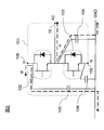
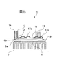
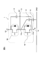
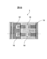
- FIG. 3A It is an electric circuit diagram which shows an example of the inverter circuit to which the semiconductor module which concerns on one embodiment of this invention is applied. It is an electric circuit diagram for demonstrating a common mode electric current. It is a side view which shows the semiconductor module which concerns on one embodiment of this invention. It is a top view of FIG. 3A.
- FIG. 4 is an electric circuit diagram for explaining the function and effect of the semiconductor module of FIGS. 3A and 3B.
- FIG. 6 is a side view showing a modification of the semiconductor module of FIGS. It is a top view of Drawing 5A. It is a side view which shows the semiconductor module which concerns on other embodiment of this invention.
- FIG. 6B is a plan view of FIG. 6A.
- FIG. 6B is an electric circuit diagram for explaining the function and effect of the semiconductor module of FIGS. 6A and 6B.
- the present invention relates to a power module that constitutes a switch portion of a power converter using a wide gap semiconductor element such as SiC, and a heat sink that cools the power module.
- a wide gap semiconductor element such as SiC
- a heat sink that cools the power module.
- the common mode current radiates noise proportional to the current amplitude and the loop area through which the current flows to the outside, and can be a major factor that makes it difficult to comply with the EMC (Electro-Magnetic Compatibility) standard.
- EMC Electro-Magnetic Compatibility
- the present invention by stacking a plurality of insulating members and AC electrode patterns, P electrode patterns, and N electrode patterns and connecting them to the heat sink, the amplitude of the common mode current is reduced and the cooling path is reduced. Reduces radiation noise without increasing the size of the heat sink.
- FIG. 1 shows a three-phase inverter circuit as an example of a system to which a semiconductor module according to an embodiment of the present invention is applied.
- the semiconductor module 1 of this example is a 2-in-1 module having a voltage switching mechanism for one phase, and a specific configuration described below is shown as a 2-in-1 module.
- the semiconductor module according to the present invention has a function of a plurality of phases.
- the integrated semiconductor module may be sufficient.
- the power conversion system shown in FIG. 1 converts first power, such as a supply battery BT, into second power using a smoothing capacitor C and a power conversion device INV, and supplies this to a three-phase AC motor M.
- the regenerative power of the phase AC motor M is converted to the first power by the power converter INV and the smoothing capacitor C, thereby charging the supply battery BT.
- a P-side semiconductor element 102 and an N-side semiconductor element 103 composed of a switching element and a rectifier element are, for example, a MOSFET (Metal-Oxide-Semiconductor-Field-Effect-Transistor), JFET (Junction-gate) using a wide band gap semiconductor such as SiC or GaN. It consists of elements such as Field-Effect (Transistor), BJT (Bipolar Junction Transistor), IGBT (Insulated Gate Bipolar Transistor), and diode.
- MOSFET Metal-Oxide-Semiconductor-Field-Effect-Transistor
- JFET Joint-gate
- the AC terminal unit 107 changes from several volts to the power supply voltage in a short time, and a common mode current as indicated by a dotted arrow line A flows through the stray capacitance 104 between the AC electrode pattern and the GND due to the voltage change.
- a current flows through the stray capacitance 105 between the P electrode pattern and GND, and a common mode current as indicated by the dotted arrow line B flows.
- the common mode current flows through a load ground capacitance (not shown), a power source ground capacitance (not shown), a stray capacitance 106 between the N electrode pattern and GND, and the like. It flows through the high voltage system and GND, and radiates noise to the outside. The amplitude of this radiation noise is proportional to the amplitude of the common mode current and the loop area that flows.
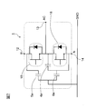
- FIG. 4 is an electric circuit diagram including the stray capacitance, showing the semiconductor module according to the first embodiment of the present invention.
- the semiconductor module 1 of this example includes a P-side semiconductor element 16 and an N-side semiconductor element 18 each composed of a switching element and a rectifier diode, and a heat sink 7, and a P terminal 12 electrically connected to the first power system. And an N terminal 14 and an AC terminal 13 electrically connected to the second power system.
- 4 is a stray capacitance between the AC electrode pattern 11 to which the AC terminal 13 is connected and the ground GND
- 5 is a stray capacitance between the P electrode pattern 10 to which the P terminal 12 is connected and the ground GND
- 6 Indicates stray capacitances between the N electrode pattern 9 connected to the N terminal 14 and the ground GND.
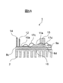
- FIG. 3A is a side view showing the semiconductor module according to the first embodiment shown in FIG. 4,
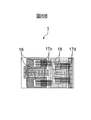
- FIG. 3B is a plan view, and the semiconductor module 1 of this example has a heat sink 7 connected to the ground GND, and this heat sink 7 is connected to an N electrode pattern 9 via an insulating layer 8a, and a P electrode pattern 10 and an AC electrode pattern 11 are connected thereto via another insulating layer 8b.
- a P terminal 12 for current input / output is mounted on the P electrode pattern 10
- an AC terminal 13 for current input / output is mounted on the AC electrode pattern 11
- an N terminal for current input / output is mounted on the N electrode pattern 9.
- a terminal 14 is mounted.
- the electrode patterns 9, 10, 11 and the insulating layers 8a, 8b are preferably formed of a multilayer ceramic substrate using silicon nitride.
- a metal pattern 15 for connection is provided on the surface in contact with the heat sink 7, and the multilayer ceramic substrate and the heat sink 7 are electrically and mechanically connected by soldering or brazing.
- the electrode formed on the lower surface of the P-side semiconductor element 16 is mounted on the upper surface of the illustrated P electrode pattern 10 so as to be electrically connected.
- the electrode formed on the upper surface of the P-side semiconductor element 16 is AC
- the electrode pattern 11 is electrically connected by a bonding wire 17a or the like.
- an electrode formed on the lower surface of the N-side semiconductor element 18 is mounted on the upper surface of the AC electrode pattern 11 shown in the figure so as to be electrically connected.
- the electrode formed on the upper surface of the N-side semiconductor element 18 is The N electrode pattern 9 is electrically connected by a bonding wire 17b or the like.
- the switching element of the P-side semiconductor element 16 and the N-side semiconductor element 18 is connected with a signal line output from the drive circuit to an electrode for inputting the switching signal.
- the multilayer insulating substrate is surrounded by a case and sealed with an insulating material.
- the N electrode pattern 9 is provided on the grounded heat sink 7 via the insulating layer 8a, and the P electrode pattern 10 and the AC electrode pattern 11 are provided on the N electrode pattern 9 via the insulating layer 8b.
- the stray capacitance 4 between the AC electrode pattern 11 and the N electrode pattern 9 is The circuit configuration is such that the stray capacitance 6 between the N electrode pattern 9 and the ground GND is connected in series.
- the stray capacitance between the P electrode pattern 10 and the ground GND is such that the stray capacitance 5 between the P electrode pattern 10 and the ground GND and the stray capacitance 6 between the N electrode pattern 9 and the ground GND are in series.
- the circuit configuration is connected to.
- the insulating layer 8b is increased by one layer in this example, the P electrode pattern 10 and the N electrode pattern 9, and the AC electrode pattern 11 and the N electrode pattern 9 are connected with low resistance, respectively. Therefore, the decrease in cooling performance is negligible.
- the N electrode pattern 9 is provided with a through hole 19 in the upper insulating layer 8b of the multilayer ceramic substrate as shown in FIG. 5 in order to facilitate the removal of the N terminal 14 and the connection with the N-side semiconductor element 18.
- a part of the N electrode pattern 9 may be disposed on the upper surface of the insulating layer 8b.
- FIG. 6A is a side view showing a semiconductor module according to the second embodiment of the present invention
- FIG. 6B is a plan view.
- the semiconductor module 1 of the present example has a heat sink 7 connected to the ground GND, and an N electrode pattern 9a and a P electrode pattern 10a are connected to the heat sink 7 via an insulating layer 8c, and another electrode is formed thereon.
- the AC electrode pattern 11a is connected through the insulating layer 8d.
- a P terminal 12 for current input / output is mounted on the P electrode pattern 10a
- an AC terminal 13 for current input / output is mounted on the AC electrode pattern 11a
- an N terminal for current input / output is mounted on the N electrode pattern 9a.
- a terminal 14 is mounted.
- the stacked positions of the P electrode patterns 10 and 10a are different.
- Each electrode pattern 9a, 10a, 11a and insulating layers 8c, 8d are preferably formed of a multilayer ceramic substrate using silicon nitride.
- a metal pattern 15 for connection is provided on the surface in contact with the heat sink 7, and the multilayer ceramic substrate and the heat sink 7 are electrically and mechanically connected by soldering or brazing.
- the electrode formed on the lower surface of the P-side semiconductor element 16 is mounted on the upper surface of the P electrode pattern 10a shown in the figure so as to be electrically connected. It is electrically connected to the electrode pattern 11a by a bonding wire 17c. Further, the electrode formed on the lower surface of the N-side semiconductor element 18 is mounted on the upper surface of the AC electrode pattern 11a shown in the figure so as to be electrically connected. The electrode formed on the upper surface of the N-side semiconductor element 18 is The N electrode pattern 9a is electrically connected by a bonding wire or the like 17d.
- the switching element of the P-side semiconductor element 16 and the N-side semiconductor element 17 is connected with a signal line output from the drive circuit to an electrode for inputting the switching signal.
- the multilayer insulating substrate is surrounded by a case and sealed with an insulating material.
- the area of the P electrode pattern 10a and the area of the N electrode pattern 9a in the plan view of FIG. 6B are configured to be the same or substantially the same, and the N electrode pattern 9a exists below the AC electrode pattern 11a.
- the portion not to be filled is filled with the same ceramic base material as the insulating layer 8c.
- the stray capacitance 5a between the P electrode pattern 10a and the ground GND becomes larger than that in the first embodiment, but the N electrode pattern 9a and the ground
- the stray capacitance 6a between the GND and the GND becomes smaller than that in the first embodiment, and at the same time, the stray capacitance 6a between the P electrode pattern 10a and the ground GND is equivalent.
- the common mode current generated in the semiconductor module of a certain phase (each phase of U, V, W) does not flow to the supply battery BT side or the motor M side, but floats in the semiconductor module of another phase nearby. Can be circulated to capacity. As a result, the loop area of the common mode current is reduced.
- the stray capacitance 6a between the N electrode pattern 9a and the ground GND is reduced, the AC pattern 11a and the ground GND, which are series capacitances of the stray capacitance 4a between the AC electrode pattern 11a and the N electrode pattern 9a. Since the stray capacitance between them (the total capacitance of the stray capacitance 4a and the stray capacitance 6a) is also reduced, the amplitude of the common mode current is also reduced. Thereby, radiation noise is reduced.
- the AC electrode patterns 11 and 11a that cause leakage current to the ground GND are grounded via the N electrode patterns 9 and 9a. Therefore, the capacitance with respect to the GND of the AC electrode patterns 11 and 11a is reduced, thereby suppressing the common mode current.
- the P electrode patterns 10 and 10a that cause the leakage current after the AC electrode patterns 11 and 11a are grounded via the N electrode patterns 9 and 9a, Since the capacitance with respect to the P electrode patterns 9 and 9a is reduced and the inductance between the PN terminals is reduced, the voltage variation of the P electrode patterns 9 and 9a during the switching transient is suppressed, thereby suppressing the common mode current. be able to.
- the GND capacity of the P electrode pattern 10a is equal to the GND capacity of the N electrode pattern 9a, so that the common mode current circulates between adjacent semiconductor modules. As a result, the loop area is reduced and radiation noise can be suppressed.
- connection area area overlapping in the stacking direction
- the inductance is increased.
- the heat resistance from the P electrode pattern 10 to the heat sink 7 and from the AC electrode pattern 11 to the heat sink 7 is reduced, so that the heat sink 7 can be reduced in size.
- the power conversion device has been described by taking an example of an inverter that performs so-called DC-AC conversion.
- DC-DC conversion DC-DC conversion
- DC-DC conversion or the like can provide the same operation and effect.
- the supply battery BT corresponds to the first power system according to the present invention
- the P terminal 12 and the N terminal 14 correspond to the first terminal according to the present invention
- the motor M corresponds to the second power system according to the present invention.
- the AC terminal 13 corresponds to the second terminal according to the present invention
- the P electrode pattern 10, 10a corresponds to the first electrode according to the present invention
- the N electrode pattern 9, 9a corresponds to the power system.
- the AC electrode patterns 11 and 11a correspond to the output electrode according to the present invention
- the insulating layers 8a and 8c correspond to the first insulating member according to the present invention.
- the insulating layers 8b and 8d correspond to the second insulating member according to the present invention.
Landscapes
- Inverter Devices (AREA)
- Shielding Devices Or Components To Electric Or Magnetic Fields (AREA)
- Cooling Or The Like Of Semiconductors Or Solid State Devices (AREA)
- Chemical & Material Sciences (AREA)
- Engineering & Computer Science (AREA)
- Ceramic Engineering (AREA)
Abstract
第1の電力系BTに電気的に接続される第1の端子12,14と第2の電力系Mに電気的に接続される第2の端子13とを有し、互いに直列に接続された一対の半導体素子16,18と、ヒートシンク7と、前記第1の端子の一方の第1の端子12と、前記一対の半導体素子の一方の半導体素子16の一方の電極とのそれぞれに電気的に接続された第1の電極10と、前記第2の端子13と、前記一対の半導体素子の他方の半導体素子18の一方の電極とのそれぞれに電気的に接続された出力電極11と、前記第1の端子の他方の第1の端子14に電気的に接続された第2の電極9と、を備える半導体モジュールであって、前記第2の電極9が、第1の絶縁部材8aを介して前記ヒートシンク7に接続され、前記出力電極11が、第2の絶縁部材8bを介して前記第2の電極9に接続されている。
Description
本発明は、半導体モジュールに関するものである。
冷却フィン(ヒートシンク)の材質に、たとえばセラミックスなどを利用し、電力変換装置(インバータ)の対地浮遊容量を低減することで、ノイズの原因となる漏れ電流を低減できる電力変換装置が知られている(特許文献1)。
しかしながら、上記従来技術の構成では、冷却フィンを金属で形成した場合と比べて、電力変換装置の対地浮遊容量は低減できるが、たとえばセラミックスの熱伝導率は金属の熱伝導率よりも低いので、電力変換装置を充分に冷却できないおそれがあった。
本発明の目的は、電力変換装置の対地浮遊容量を低減するとともに、電力変換装置を冷却する性能が低下することを防止することである。
本発明は、出力電極を、絶縁部材を介して第2の電極に接続し、第2の電極を他の絶縁部材を介してヒートシンクに接続することによって、上記目的を達成する。
本発明によれば、出力電極が第2の電極を介して接地されることになり、出力電極と接地との間の浮遊容量と第2の電極と接地との間の浮遊容量が直列に接続された回路構成となるので、コモンモード電流を低減することができるとともに、出力電極と第2の電極が低抵抗で接続しているため、電力変換装置を冷却する性能が低下することを防止できる。
本発明は、例えばSiCなどのワイドギャップ半導体素子を用いた電力変換器のスイッチ部分を構成するパワーモジュールと、これを冷却するヒートシンクに関するものである。ワイドギャップ半導体素子を用いた電力変換器においては、その素子の特性を生かして小型化するために、電源電圧を高電圧化し、損失を低減するために素子のターンオン/オフを高速にすることが求められる。
しかしながら、高電圧の変換器は接地(以下、GNDともいう)から絶縁する必要があり、電源電圧を高くし、ターンオン/オフを高速にすると、単位時間当たり電圧変化量(dV/dt)が大きくなり、パワーモジュールとGND間の絶縁層に浮遊する静電容量に流れる電流が増大するという問題がある。
この静電容量に流れる電流Icmは静電容量CとdV/dtを用いて、Icm=C×(dV/dt)で表すことができ、高電圧の系からGNDに漏洩するコモンモード電流として定義される。コモンモード電流は、その電流振幅と電流が流れるループ面積に比例したノイズを外部に放射するため、EMC(Electro-Magnetic Compatibility)規格を準拠するのが困難になる主要因となり得る。一方で、電力変換器を小型化するためには、変換器体積の大部分を占めるヒートシンクを小さくすることが求められる。
このため本発明では、複数の絶縁部材とAC電極パターン,P電極パターン,N電極パターンを積層してヒートシンクに接続することで、コモンモード電流の振幅を低減するとともに、冷却経路を小さくすることによりヒートシンクを大型化することなく放射ノイズを低減する。
以下、本発明の一実施の形態を、図面に基づき詳細に説明する。図1に本発明の一実施の形態に係る半導体モジュールを適用したシステムの例として、3相のインバータ回路を示す。本例の半導体モジュール1は、1相分の電圧切り替え機構を備える2in1モジュールであり、以下に説明する具体的な構成は2in1モジュールで示すが、本発明に係る半導体モジュールは、複数相の機能をまとめた半導体モジュールであってもよい。
図1に示す電力変換システムは、供給電池BTなどの第1の電力を平滑用コンデンサCおよび電力変換装置INVにより第2の電力に変換し、これを三相交流モータMに供給したり、三相交流モータMの回生電力を電力変換装置INVおよび平滑用コンデンサCにより第1の電力に変換し、これにより供給電池BTを充電したりするものである。
まず、従来構造の半導体モジュール101を示す図2を参照して、コモンモード電流について説明する。スイッチング素子と整流素子からなるP側半導体素子102とN側半導体素子103は、例えばSiCやGaN等のワイドバンドギャップ半導体を用いたMOSFET(Metal-Oxide-Semiconductor Field-Effect Transistor),JFET(Junction gate Field-Effect Transistor),BJT(Bipolar Junction Transistor),IGBT(Insulated Gate Bipolar Transistor),ダイオード等の素子で構成される。
これらは制御信号に応じて電源電圧をON/OFFし、交流の電力を生成する。その際、AC端子部107は短時間で数Vから電源電圧まで変化し、その電圧変化によりAC電極パターンとGND間の浮遊容量104に点矢印線Aで示すようなコモンモード電流が流れる。
また、スイッチング過渡時にはP端子108の電圧も変動するため、P電極パターンとGND間の浮遊容量105に電流が流れ、点矢印線Bで示すようなコモンモード電流が流れる。同様の現象が各相の半導体モジュールにおいて発生し、コモンモード電流は負荷の対地容量(図示せず)、電源の対地容量(図示せず)、N電極パターンとGND間の浮遊容量106等を介して高電圧の系とGNDを流れ、外部にノイズを放射する。そしてこの放射ノイズの振幅は、コモンモード電流の振幅と流れるループ面積に比例する。
《第1実施形態》
図4は、本発明の第1実施形態に係る半導体モジュールを示す、浮遊容量を含む電気回路図である。本例の半導体モジュール1は、それぞれスイッチング素子と整流ダイオードからなるP側半導体素子16およびN側半導体素子18と、ヒートシンク7とを備え、第1の電力系に電気的に接続されるP端子12およびN端子14と、第2の電力系に電気的に接続されるAC端子13とが設けられている。なお、4は、AC端子13が接続されたAC電極パターン11と接地GNDとの間の浮遊容量、5はP端子12が接続されたP電極パターン10と接地GNDとの間の浮遊容量、6はN端子14が接続されたN電極パターン9と接地GNDとの間の浮遊容量をそれぞれ示す。
図4は、本発明の第1実施形態に係る半導体モジュールを示す、浮遊容量を含む電気回路図である。本例の半導体モジュール1は、それぞれスイッチング素子と整流ダイオードからなるP側半導体素子16およびN側半導体素子18と、ヒートシンク7とを備え、第1の電力系に電気的に接続されるP端子12およびN端子14と、第2の電力系に電気的に接続されるAC端子13とが設けられている。なお、4は、AC端子13が接続されたAC電極パターン11と接地GNDとの間の浮遊容量、5はP端子12が接続されたP電極パターン10と接地GNDとの間の浮遊容量、6はN端子14が接続されたN電極パターン9と接地GNDとの間の浮遊容量をそれぞれ示す。
図3Aは図4に示す第1実施形態に係る半導体モジュールを示す側面図、図3Bは平面図であり、本例の半導体モジュール1は、接地GNDに接続されるヒートシンク7を有し、このヒートシンク7の上に絶縁層8aを介してN電極パターン9が接続され、その上に他の絶縁層8bを介してP電極パターン10とAC電極パターン11が接続されている。そして、P電極パターン10には電流入出力用のP端子12が実装され、AC電極パターン11には電流入出力用のAC端子13が実装され、N電極パターン9には電流入出力用のN端子14が実装されている。
各電極パターン9,10,11と絶縁層8a,8bは、好適には窒化珪素を用いた多層セラミック基板で構成されている。また、ヒートシンク7と接する面には接続用の金属パターン15が設けられ、多層セラミック基板とヒートシンク7を半田付けまたはロウ付けにより電気的にも機械的にも接続した構成とされている。
図示するP電極パターン10の上面には、P側半導体素子16の下面に形成された電極が電気的に接続されるように実装され、P側半導体素子16の上面に形成された電極は、AC電極パターン11に対してボンディングワイヤ17a等で電気的に接続されている。また、図示するAC電極パターン11の上面には、N側半導体素子18の下面に形成された電極が電気的に接続されるように実装され、N側半導体素子18の上面に形成された電極は、N電極パターン9に対してボンディングワイヤ17b等で電気的に接続されている。
なお図示はしないが、P側半導体素子16およびN側半導体素子18のうちのスイッチング素子には、そのスイッチング信号を入力する電極に駆動回路から出力される信号線が接続されている。また図示はしないが、多層絶縁基板はケースに囲まれ、絶縁性材料により封止されている。
以上のように、接地されるヒートシンク7の上に絶縁層8aを介してN電極パターン9を設け、このN電極パターン9の上に絶縁層8bを介してP電極パターン10とAC電極パターン11を設けることにより、図4に示すコモンモード電流の大きさの原因となるAC電極パターン11と接地GNDとの間の浮遊容量は、AC電極パターン11とN電極パターン9との間の浮遊容量4と、N電極パターン9と接地GNDとの間の浮遊容量6とが直列に接続された回路構成になる。また、P電極パターン10と接地GNDとの間の浮遊容量は、P電極パターン10と接地GNDとの間の浮遊容量5と、N電極パターン9と接地GNDとの間の浮遊容量6とが直列に接続された回路構成になる。
2つ以上のコンデンサC1,C2を接続する場合に、全体のコンデンサ容量Cは、並列に接続した場合がC=C1+C2+…であるのに対し、直列に接続した場合はC=1/C1+1/C2+…となり、直列に接続した方が、静電容量が小さくなる。したがって、本例の半導体モジュール1では直列接続されることにより浮遊容量が小さくなり、これによりIcm=C×(dV/dt)で表されるコモンモード電流も小さくなる。
一方、冷却の観点においても、本例では絶縁層8bが1層多くなるものの、P電極パターン10とN電極パターン9、およびAC電極パターン11とN電極パターン9はそれぞれ低抵抗で接続されているため、冷却性能の減少はごく僅かである。
さらに、図3に示すようにP端子12からAC電極パターン11を経てN端子14に至る電流経路は、対向した構成となっているため、P端子12とN端子14との間が低インダクタンスである。このため、スイッチング過渡時のP端子12の電圧変動を抑制することができる。
なお、N電極パターン9は、N端子14の取り出しやN側半導体素子18との接続を容易にするために、図5に示すように多層セラミック基板の上側の絶縁層8bにスルーホール19を設け、N電極パターン9の一部を絶縁層8bの上面に配置してもよい。
《第2実施形態》
図6Aは本発明の第2実施形態に係る半導体モジュールを示す側面図、図6Bは平面図である。本例の半導体モジュール1は、接地GNDに接続されるヒートシンク7を有し、このヒートシンク7の上に絶縁層8cを介してN電極パターン9aおよびP電極パターン10aが接続され、その上に他の絶縁層8dを介してAC電極パターン11aが接続されている。そして、P電極パターン10aには電流入出力用のP端子12が実装され、AC電極パターン11aには電流入出力用のAC端子13が実装され、N電極パターン9aには電流入出力用のN端子14が実装されている。上述した図3A,図3Bに示す第1実施形態の半導体モジュール1に比べ、P電極パターン10,10aの積層位置が相違する。
図6Aは本発明の第2実施形態に係る半導体モジュールを示す側面図、図6Bは平面図である。本例の半導体モジュール1は、接地GNDに接続されるヒートシンク7を有し、このヒートシンク7の上に絶縁層8cを介してN電極パターン9aおよびP電極パターン10aが接続され、その上に他の絶縁層8dを介してAC電極パターン11aが接続されている。そして、P電極パターン10aには電流入出力用のP端子12が実装され、AC電極パターン11aには電流入出力用のAC端子13が実装され、N電極パターン9aには電流入出力用のN端子14が実装されている。上述した図3A,図3Bに示す第1実施形態の半導体モジュール1に比べ、P電極パターン10,10aの積層位置が相違する。
各電極パターン9a,10a,11aと絶縁層8c,8dは、好適には窒化珪素を用いた多層セラミック基板で構成されている。また、ヒートシンク7と接する面には接続用の金属パターン15が設けられ、多層セラミック基板とヒートシンク7を半田付けまたはロウ付けにより電気的にも機械的にも接続した構成とされている。
図示するP電極パターン10aの上面には、P側半導体素子16の下面に形成された電極が電気的に接続されるように実装され、P側半導体素子16の上面に形成された電極は、AC電極パターン11aに対してボンディングワイヤ等17cで電気的に接続されている。また、図示するAC電極パターン11aの上面には、N側半導体素子18の下面に形成された電極が電気的に接続されるように実装され、N側半導体素子18の上面に形成された電極は、N電極パターン9aに対してボンディングワイヤ等17dで電気的に接続されている。
なお図示はしないが、P側半導体素子16およびN側半導体素子17のうちのスイッチング素子には、そのスイッチング信号を入力する電極に駆動回路から出力される信号線が接続されている。また図示はしないが、多層絶縁基板はケースに囲まれ、絶縁性材料により封止されている。
特に本例の半導体モジュール1では、図6Bの平面視におけるP電極パターン10aの面積とN電極パターン9aの面積が同一または略同一に構成され、AC電極パターン11aの下層においてN電極パターン9aが存在しない部分は絶縁層8cと同様のセラミック基材が充填されている。
以上のように構成にすることにより、図7に示す電気回路において、P電極パターン10aと接地GNDとの間の浮遊容量5aが第1実施形態に比べて大きくなるが、N電極パターン9aと接地GNDとの間の浮遊容量6aが第1実施形態に比べて小さくなると同時にP電極パターン10aと接地GNDとの間の浮遊容量5aと同等になる。これにより、ある相(U,V,Wの各相)の半導体モジュールで発生したコモンモード電流が供給電池BT側やモータM側に流れることなく、近くにある他の相の半導体モジュール内の浮遊容量に循環させることができる。その結果、コモンモード電流のループ面積が小さくなる。
また、N電極パターン9aと接地GNDとの間の浮遊容量6aが小さくなることにより、AC電極パターン11aとN電極パターン9aとの間の浮遊容量4aとの直列容量であるACパターン11aと接地GNDとの間の浮遊容量(浮遊容量4aと浮遊容量6aの総容量)も小さくなるため、コモンモード電流の振幅も小さくなる。これにより、放射ノイズが低減される。
以上のとおり、上記第1実施形態および第2実施形態の半導体モジュール1では、接地GNDへの漏洩電流の原因となるAC電極パターン11,11aがN電極パターン9,9aを介して接地されているので、AC電極パターン11,11aの対GND容量が小さくなり、これによりコモンモード電流を抑制することができる。
また、上記第1実施形態の半導体モジュール1では、AC電極パターン11,11aの次に漏洩電流の原因となるP電極パターン10,10aがN電極パターン9,9aを介して接地されているので、P電極パターン9,9aの対GND容量が小さくなるとともに、PN端子間のインダクタンスが減少するため、スイッチング過渡時のP電極パターン9,9aの電圧変動が抑制され、これによりコモンモード電流を抑制することができる。
また、上記第2実施形態の半導体モジュール1によれば、P電極パターン10aの対GND容量とN電極パターン9aの対GND容量が同等になるので、コモンモード電流が、近接する半導体モジュール間で循環することになり、その結果ループ面積が小さくなって放射ノイズを抑制することができる。
さらに、図5Aおよび図5Bに示す半導体モジュール1によれば、P電極パターン10およびAC電極パターン11と、N電極パターン9との接続面積(積層方向に重なった面積)が広くなるので、インダクタンスが低減するとともに、P電極パターン10からヒートシンク7、AC電極パターン11からヒートシンク7までの熱抵抗が小さくなるため、ヒートシンク7を小型化することができる。
なお、上記実施形態では、電力変換装置をいわゆる直流-交流変換が行われるインバータを例に説明したが、たとえば直流-直流変換(DC-DC変換)などでも同様の作用効果を得ることができる。
上記供給電池BTが本発明に係る第1の電力系に相当し、上記P端子12およびN端子14が本発明に係る第1の端子に相当し、上記モータMが本発明に係る第2の電力系に相当し、上記AC端子13が本発明に係る第2の端子に相当し、上記P電極パターン10,10aが本発明に係る第1の電極に相当し、上記N電極パターン9,9aが本発明に係る第2の電極に相当し、上記AC電極パターン11,11aが本発明に係る出力電極に相当し、上記絶縁層8a,8cが本発明に係る第1の絶縁部材に相当し、上記絶縁層8b,8dが本発明に係る第2の絶縁部材に相当する。
1:半導体モジュール
2:P側半導体素子
3:N側半導体素子
4,5,6,4a,5a,6a:浮遊容量
7:ヒートシンク
8a,8b,8c,8d:絶縁層
9,9a:N電極パターン
10,10a:P電極パターン
11,11a:AC電極パターン
12:P端子
13:AC端子
14:N端子
15:金属パターン
16:P側半導体素子
17a,17b:ボンディングワイヤ
18:N側半導体素子
19:スルーホール
BT:二次電池
C:平滑用コンデンサ
M:モータ
INV:電力変換部
2:P側半導体素子
3:N側半導体素子
4,5,6,4a,5a,6a:浮遊容量
7:ヒートシンク
8a,8b,8c,8d:絶縁層
9,9a:N電極パターン
10,10a:P電極パターン
11,11a:AC電極パターン
12:P端子
13:AC端子
14:N端子
15:金属パターン
16:P側半導体素子
17a,17b:ボンディングワイヤ
18:N側半導体素子
19:スルーホール
BT:二次電池
C:平滑用コンデンサ
M:モータ
INV:電力変換部
Claims (4)
- 第1の電力系に電気的に接続される第1の端子と第2の電力系に電気的に接続される第2の端子とを有し、互いに直列に接続された一対の半導体素子と、
ヒートシンクと、
前記第1の端子の一方の第1の端子と、前記一対の半導体素子の一方の半導体素子の一方の電極とのそれぞれに電気的に接続された第1の電極と、
前記第2の端子と、前記一対の半導体素子の他方の半導体素子の一方の電極とのそれぞれに電気的に接続された出力電極と、
前記第1の端子の他方の第1の端子に電気的に接続された第2の電極と、
を備える半導体モジュールであって、
前記一方の半導体素子の他方の電極が、前記出力電極に電気的に接続され、
前記他方の半導体素子の他方の電極が、前記第2の電極に電気的に接続され、
前記第2の電極が、第1の絶縁部材を介して前記ヒートシンクに接続され、
前記出力電極が、第2の絶縁部材を介して前記第2の電極に接続されている半導体モジュール。 - 前記第1の電極は、前記第2の絶縁部材を介して前記第2の電極に接続されている請求項1に記載の半導体モジュール。
- 前記第1の電極は、前記第1の絶縁部材を介して前記ヒートシンクに接続され、
前記第1の電極の面積と前記第2の電極の面積が略同一である請求項1に記載の半導体モジュール。 - 前記第2の電極は、
前記出力電極と同一面に形成された電極と、
前記第1の絶縁部材上に形成された電極と、
これら2つの電極を電気的に接続するスルーホールと、を含む請求項1~3のいずれか一項に記載の半導体モジュール。
Priority Applications (3)
| Application Number | Priority Date | Filing Date | Title |
|---|---|---|---|
| CN201280039872.8A CN103782380B (zh) | 2011-08-25 | 2012-08-24 | 半导体模块 |
| US14/236,236 US8921998B2 (en) | 2011-08-25 | 2012-08-24 | Semiconductor module |
| EP12825114.7A EP2750184B1 (en) | 2011-08-25 | 2012-08-24 | Semiconductor module |
Applications Claiming Priority (2)
| Application Number | Priority Date | Filing Date | Title |
|---|---|---|---|
| JP2011184019A JP5798412B2 (ja) | 2011-08-25 | 2011-08-25 | 半導体モジュール |
| JP2011-184019 | 2011-08-25 |
Publications (1)
| Publication Number | Publication Date |
|---|---|
| WO2013027819A1 true WO2013027819A1 (ja) | 2013-02-28 |
Family
ID=47746554
Family Applications (1)
| Application Number | Title | Priority Date | Filing Date |
|---|---|---|---|
| PCT/JP2012/071398 Ceased WO2013027819A1 (ja) | 2011-08-25 | 2012-08-24 | 半導体モジュール |
Country Status (5)
| Country | Link |
|---|---|
| US (1) | US8921998B2 (ja) |
| EP (1) | EP2750184B1 (ja) |
| JP (1) | JP5798412B2 (ja) |
| CN (1) | CN103782380B (ja) |
| WO (1) | WO2013027819A1 (ja) |
Families Citing this family (27)
| Publication number | Priority date | Publication date | Assignee | Title |
|---|---|---|---|---|
| JP2016012973A (ja) * | 2014-06-27 | 2016-01-21 | 株式会社オートネットワーク技術研究所 | 回路装置 |
| CN106489203B (zh) | 2014-07-03 | 2018-09-18 | 日产自动车株式会社 | 半桥式功率半导体模块及其制造方法 |
| WO2016042903A1 (ja) * | 2014-09-17 | 2016-03-24 | 富士電機株式会社 | 半導体モジュール |
| JP2016061661A (ja) * | 2014-09-17 | 2016-04-25 | 富士電機株式会社 | 圧力センサ装置および圧力センサ装置の製造方法 |
| JP6327105B2 (ja) | 2014-10-17 | 2018-05-23 | 三菱電機株式会社 | 半導体装置 |
| JP6288301B2 (ja) * | 2014-11-28 | 2018-03-14 | 日産自動車株式会社 | ハーフブリッジパワー半導体モジュール及びその製造方法 |
| JP2016115900A (ja) * | 2014-12-18 | 2016-06-23 | 三菱電機株式会社 | 半導体モジュールおよび半導体装置 |
| CN104867888A (zh) * | 2015-05-04 | 2015-08-26 | 嘉兴斯达半导体股份有限公司 | 一种高散热性SiC的功率模块 |
| WO2017002390A1 (ja) * | 2015-06-30 | 2017-01-05 | シャープ株式会社 | 回路モジュール |
| EP3226014B1 (en) * | 2016-03-30 | 2024-01-10 | Mitsubishi Electric R&D Centre Europe B.V. | Method for estimating a level of damage or a lifetime expectation of a power semiconductor module comprising at least one die |
| US10404186B2 (en) | 2016-10-27 | 2019-09-03 | General Electric Company | Power module systems and methods having reduced common mode capacitive currents and reduced electromagnetic interference |
| JP6809294B2 (ja) * | 2017-03-02 | 2021-01-06 | 三菱電機株式会社 | パワーモジュール |
| JP2018195694A (ja) * | 2017-05-17 | 2018-12-06 | 株式会社Soken | 電力変換器 |
| JP6888468B2 (ja) * | 2017-08-01 | 2021-06-16 | 富士電機株式会社 | 鉄道車両用電力変換装置 |
| JP7252705B2 (ja) * | 2017-09-28 | 2023-04-05 | デンカ株式会社 | 多層回路基板及びその製造方法 |
| JP6954029B2 (ja) * | 2017-11-15 | 2021-10-27 | 富士電機株式会社 | 電力変換装置および鉄道車両用電力変換装置 |
| JP2019091804A (ja) | 2017-11-15 | 2019-06-13 | シャープ株式会社 | パワー半導体モジュールおよび電子機器 |
| US10411609B2 (en) * | 2017-12-22 | 2019-09-10 | Panasonic Intellectual Property Management Co., Ltd. | Substrate mounted inverter device |
| CN111199959B (zh) | 2018-11-19 | 2021-11-02 | 台达电子企业管理(上海)有限公司 | 功率模块的封装结构 |
| US11735514B2 (en) | 2019-06-26 | 2023-08-22 | Mitsubishi Electric Corporation | Semiconductor device and power conversion device |
| TWI735179B (zh) * | 2020-03-11 | 2021-08-01 | 佳世達科技股份有限公司 | 電子裝置與其減低漏電流方法 |
| JP7318615B2 (ja) * | 2020-09-11 | 2023-08-01 | トヨタ自動車株式会社 | 電力変換装置 |
| FR3131503B1 (fr) * | 2021-12-28 | 2025-09-12 | Thales Sa | Composant de puissance à filtrage local et convertisseur mettant en œuvre plusieurs composants de puissance à filtrage local |
| CN114725055A (zh) * | 2022-02-28 | 2022-07-08 | 华为数字能源技术有限公司 | 一种功率模块、电力系统和电子设备 |
| CN119234308A (zh) * | 2022-05-19 | 2024-12-31 | 华为数字能源技术有限公司 | 具有共模传导发射屏蔽的功率转换器封装件 |
| JP2024015805A (ja) * | 2022-07-25 | 2024-02-06 | マツダ株式会社 | スイッチングデバイスおよびスイッチングモジュール |
| CN120072785A (zh) * | 2023-11-28 | 2025-05-30 | 华为数字能源技术有限公司 | 功率模组以及光伏优化器 |
Citations (7)
| Publication number | Priority date | Publication date | Assignee | Title |
|---|---|---|---|---|
| JP2000031325A (ja) * | 1998-07-13 | 2000-01-28 | Hitachi Ltd | 半導体パワーモジュール及びこれを用いたインバータ装置 |
| JP2005020868A (ja) * | 2003-06-25 | 2005-01-20 | Fuji Electric Fa Components & Systems Co Ltd | 電力変換回路 |
| JP3649259B2 (ja) | 1996-04-26 | 2005-05-18 | 株式会社安川電機 | インバータ装置 |
| JP2005217167A (ja) * | 2004-01-29 | 2005-08-11 | Kansai Electric Power Co Inc:The | 半導体装置及びそれを用いた電力装置 |
| JP2010016947A (ja) * | 2008-07-02 | 2010-01-21 | Fuji Electric Device Technology Co Ltd | 電力変換装置のパワーモジュール |
| JP2012015418A (ja) * | 2010-07-02 | 2012-01-19 | Honda Motor Co Ltd | 半導体装置 |
| JP2012039825A (ja) * | 2010-08-11 | 2012-02-23 | Toyo Electric Mfg Co Ltd | 電力変換装置 |
Family Cites Families (14)
| Publication number | Priority date | Publication date | Assignee | Title |
|---|---|---|---|---|
| JP2777464B2 (ja) * | 1990-07-18 | 1998-07-16 | 株式会社日立製作所 | 電子装置と、これを用いたエンジンの点火装置 |
| DE4418426B4 (de) * | 1993-09-08 | 2007-08-02 | Mitsubishi Denki K.K. | Halbleiterleistungsmodul und Verfahren zur Herstellung des Halbleiterleistungsmoduls |
| EP0661748A1 (en) * | 1993-12-28 | 1995-07-05 | Hitachi, Ltd. | Semiconductor device |
| JP3429921B2 (ja) * | 1995-10-26 | 2003-07-28 | 三菱電機株式会社 | 半導体装置 |
| JP3676268B2 (ja) * | 2001-08-01 | 2005-07-27 | 株式会社日立製作所 | 伝熱構造体及び半導体装置 |
| US6747300B2 (en) * | 2002-03-04 | 2004-06-08 | Ternational Rectifier Corporation | H-bridge drive utilizing a pair of high and low side MOSFETs in a common insulation housing |
| US6946740B2 (en) * | 2002-07-15 | 2005-09-20 | International Rectifier Corporation | High power MCM package |
| EP1594164B1 (en) * | 2003-02-14 | 2012-05-09 | Hitachi, Ltd. | Integrated circuit for driving semiconductor device |
| JP2005332874A (ja) * | 2004-05-18 | 2005-12-02 | Hitachi Metals Ltd | 回路基板及びこれを用いた半導体装置 |
| US8154114B2 (en) * | 2007-08-06 | 2012-04-10 | Infineon Technologies Ag | Power semiconductor module |
| US8018047B2 (en) * | 2007-08-06 | 2011-09-13 | Infineon Technologies Ag | Power semiconductor module including a multilayer substrate |
| JP5272191B2 (ja) * | 2007-08-31 | 2013-08-28 | 三菱電機株式会社 | 半導体装置および半導体装置の製造方法 |
| CN102339818B (zh) * | 2010-07-15 | 2014-04-30 | 台达电子工业股份有限公司 | 功率模块及其制造方法 |
| CN102340233B (zh) * | 2010-07-15 | 2014-05-07 | 台达电子工业股份有限公司 | 功率模块 |
-
2011
- 2011-08-25 JP JP2011184019A patent/JP5798412B2/ja active Active
-
2012
- 2012-08-24 US US14/236,236 patent/US8921998B2/en active Active
- 2012-08-24 EP EP12825114.7A patent/EP2750184B1/en active Active
- 2012-08-24 CN CN201280039872.8A patent/CN103782380B/zh active Active
- 2012-08-24 WO PCT/JP2012/071398 patent/WO2013027819A1/ja not_active Ceased
Patent Citations (7)
| Publication number | Priority date | Publication date | Assignee | Title |
|---|---|---|---|---|
| JP3649259B2 (ja) | 1996-04-26 | 2005-05-18 | 株式会社安川電機 | インバータ装置 |
| JP2000031325A (ja) * | 1998-07-13 | 2000-01-28 | Hitachi Ltd | 半導体パワーモジュール及びこれを用いたインバータ装置 |
| JP2005020868A (ja) * | 2003-06-25 | 2005-01-20 | Fuji Electric Fa Components & Systems Co Ltd | 電力変換回路 |
| JP2005217167A (ja) * | 2004-01-29 | 2005-08-11 | Kansai Electric Power Co Inc:The | 半導体装置及びそれを用いた電力装置 |
| JP2010016947A (ja) * | 2008-07-02 | 2010-01-21 | Fuji Electric Device Technology Co Ltd | 電力変換装置のパワーモジュール |
| JP2012015418A (ja) * | 2010-07-02 | 2012-01-19 | Honda Motor Co Ltd | 半導体装置 |
| JP2012039825A (ja) * | 2010-08-11 | 2012-02-23 | Toyo Electric Mfg Co Ltd | 電力変換装置 |
Non-Patent Citations (1)
| Title |
|---|
| See also references of EP2750184A4 |
Also Published As
| Publication number | Publication date |
|---|---|
| CN103782380A (zh) | 2014-05-07 |
| EP2750184B1 (en) | 2020-10-07 |
| US8921998B2 (en) | 2014-12-30 |
| JP2013045974A (ja) | 2013-03-04 |
| US20140159225A1 (en) | 2014-06-12 |
| EP2750184A4 (en) | 2015-08-26 |
| CN103782380B (zh) | 2019-12-13 |
| EP2750184A1 (en) | 2014-07-02 |
| JP5798412B2 (ja) | 2015-10-21 |
Similar Documents
| Publication | Publication Date | Title |
|---|---|---|
| JP5798412B2 (ja) | 半導体モジュール | |
| JP6513303B2 (ja) | 電力用半導体モジュールおよび電力変換装置 | |
| US9685879B2 (en) | Power semiconductor module and power conversion device | |
| US12438115B2 (en) | Power semiconductor module | |
| JP6425380B2 (ja) | パワー回路およびパワーモジュール | |
| US11605613B2 (en) | Semiconductor device | |
| JP6717270B2 (ja) | 半導体モジュール | |
| Jakobi et al. | Benefits of new CoolSiC TM MOSFET in HybridPACK TM Drive package for electrical drive train applications | |
| JP6962945B2 (ja) | パワー半導体モジュールおよびそれを用いた電力変換装置 | |
| US20210210477A1 (en) | Power module with organic layers | |
| US11863166B2 (en) | Power semiconductor module and power converter | |
| JP2019017112A (ja) | パワー回路 | |
| CN111696976B (zh) | 功率半导体模块衬底及其所应用的电动机车 | |
| KR20180126371A (ko) | 전력 변환기 | |
| JP2022050887A (ja) | 半導体装置 | |
| CN210516724U (zh) | 一种功率半导体模块和功率半导体器件 | |
| JP2005251839A (ja) | 電力用半導体モジュールの絶縁基板 | |
| JP2012050176A (ja) | 電力変換装置のパワーモジュール | |
| JP5119741B2 (ja) | スイッチングモジュール | |
| JP2025174867A (ja) | 半導体装置及び電力変換装置 | |
| JP2008300530A (ja) | スイッチングモジュール |
Legal Events
| Date | Code | Title | Description |
|---|---|---|---|
| 121 | Ep: the epo has been informed by wipo that ep was designated in this application |
Ref document number: 12825114 Country of ref document: EP Kind code of ref document: A1 |
|
| DPE2 | Request for preliminary examination filed before expiration of 19th month from priority date (pct application filed from 20040101) | ||
| WWE | Wipo information: entry into national phase |
Ref document number: 14236236 Country of ref document: US |
|
| NENP | Non-entry into the national phase |
Ref country code: DE |
|
| WWE | Wipo information: entry into national phase |
Ref document number: 2012825114 Country of ref document: EP |