WO2013035491A1 - スイッチ駆動回路,インバータ装置及びパワーステアリング装置 - Google Patents
スイッチ駆動回路,インバータ装置及びパワーステアリング装置 Download PDFInfo
- Publication number
- WO2013035491A1 WO2013035491A1 PCT/JP2012/070504 JP2012070504W WO2013035491A1 WO 2013035491 A1 WO2013035491 A1 WO 2013035491A1 JP 2012070504 W JP2012070504 W JP 2012070504W WO 2013035491 A1 WO2013035491 A1 WO 2013035491A1
- Authority
- WO
- WIPO (PCT)
- Prior art keywords
- circuit
- reference potential
- semiconductor switching
- switch
- switching element
- Prior art date
- Legal status (The legal status is an assumption and is not a legal conclusion. Google has not performed a legal analysis and makes no representation as to the accuracy of the status listed.)
- Ceased
Links
Images


Classifications
-
- H—ELECTRICITY
- H10—SEMICONDUCTOR DEVICES; ELECTRIC SOLID-STATE DEVICES NOT OTHERWISE PROVIDED FOR
- H10D—INORGANIC ELECTRIC SEMICONDUCTOR DEVICES
- H10D99/00—Subject matter not provided for in other groups of this subclass
-
- H—ELECTRICITY
- H02—GENERATION; CONVERSION OR DISTRIBUTION OF ELECTRIC POWER
- H02J—ELECTRIC POWER NETWORKS; CIRCUIT ARRANGEMENTS OR SYSTEMS FOR SUPPLYING OR DISTRIBUTING ELECTRIC POWER; SYSTEMS FOR STORING ELECTRIC ENERGY
- H02J7/00—Circuit arrangements for charging or discharging batteries or for supplying loads from batteries
- H02J7/60—Circuit arrangements for charging or discharging batteries or for supplying loads from batteries including safety or protection arrangements
- H02J7/68—Circuit arrangements for charging or discharging batteries or for supplying loads from batteries including safety or protection arrangements using circuits for correcting or protecting against reverse-polarity
-
- H—ELECTRICITY
- H02—GENERATION; CONVERSION OR DISTRIBUTION OF ELECTRIC POWER
- H02M—APPARATUS FOR CONVERSION BETWEEN AC AND AC, BETWEEN AC AND DC, OR BETWEEN DC AND DC, AND FOR USE WITH MAINS OR SIMILAR POWER SUPPLY SYSTEMS; CONVERSION OF DC OR AC INPUT POWER INTO SURGE OUTPUT POWER; CONTROL OR REGULATION THEREOF
- H02M7/00—Conversion of AC power input into DC power output; Conversion of DC power input into AC power output
- H02M7/42—Conversion of DC power input into AC power output without possibility of reversal
- H02M7/44—Conversion of DC power input into AC power output without possibility of reversal by static converters
- H02M7/48—Conversion of DC power input into AC power output without possibility of reversal by static converters using discharge tubes with control electrode or semiconductor devices with control electrode
- H02M7/53—Conversion of DC power input into AC power output without possibility of reversal by static converters using discharge tubes with control electrode or semiconductor devices with control electrode using devices of a triode or transistor type requiring continuous application of a control signal
- H02M7/537—Conversion of DC power input into AC power output without possibility of reversal by static converters using discharge tubes with control electrode or semiconductor devices with control electrode using devices of a triode or transistor type requiring continuous application of a control signal using semiconductor devices only, e.g. single switched pulse inverters
- H02M7/5387—Conversion of DC power input into AC power output without possibility of reversal by static converters using discharge tubes with control electrode or semiconductor devices with control electrode using devices of a triode or transistor type requiring continuous application of a control signal using semiconductor devices only, e.g. single switched pulse inverters in a bridge configuration
- H02M7/53871—Conversion of DC power input into AC power output without possibility of reversal by static converters using discharge tubes with control electrode or semiconductor devices with control electrode using devices of a triode or transistor type requiring continuous application of a control signal using semiconductor devices only, e.g. single switched pulse inverters in a bridge configuration with automatic control of output voltage or current
-
- H—ELECTRICITY
- H02—GENERATION; CONVERSION OR DISTRIBUTION OF ELECTRIC POWER
- H02P—CONTROL OR REGULATION OF ELECTRIC MOTORS, ELECTRIC GENERATORS OR DYNAMO-ELECTRIC CONVERTERS; CONTROLLING TRANSFORMERS, REACTORS OR CHOKE COILS
- H02P27/00—Arrangements or methods for the control of AC motors characterised by the kind of supply voltage
- H02P27/04—Arrangements or methods for the control of AC motors characterised by the kind of supply voltage using variable-frequency supply voltage, e.g. inverter or converter supply voltage
- H02P27/06—Arrangements or methods for the control of AC motors characterised by the kind of supply voltage using variable-frequency supply voltage, e.g. inverter or converter supply voltage using DC to AC converters or inverters
-
- H—ELECTRICITY
- H02—GENERATION; CONVERSION OR DISTRIBUTION OF ELECTRIC POWER
- H02P—CONTROL OR REGULATION OF ELECTRIC MOTORS, ELECTRIC GENERATORS OR DYNAMO-ELECTRIC CONVERTERS; CONTROLLING TRANSFORMERS, REACTORS OR CHOKE COILS
- H02P29/00—Arrangements for regulating or controlling electric motors, appropriate for both AC and DC motors
- H02P29/02—Providing protection against overload without automatic interruption of supply
- H02P29/024—Detecting a fault condition, e.g. short circuit, locked rotor, open circuit or loss of load
- H02P29/027—Detecting a fault condition, e.g. short circuit, locked rotor, open circuit or loss of load the fault being an over-current
Definitions
- Embodiments of the present invention include a switch drive circuit that outputs an open / close control signal to a switch circuit for electrically opening and closing a DC power supply and an inverter circuit, and an inverter device including the inverter circuit and the switching drive circuit And a power steering device including the inverter device.
- the electric power steering device detects the steering input torque applied through the steering wheel by the driver's operation with the steering torque sensor, and determines the magnitude and direction of the motor output in the control device based on the output signal of the steering torque sensor.
- a motor is driven via an inverter circuit, and the power of the motor is transmitted to a steering system to reduce steering torque.
- a switch configured by using a relay is inserted between a battery as a power source and an inverter circuit, and when the control device detects an overcurrent state or an abnormality in PWM control, the switch is turned off. It opens to shut off the power supply to the inverter circuit and the motor, thereby preventing an unwanted auxiliary steering force from being generated from the motor.
- a switch configured using a relay needs to supply a large current of several tens to 100 A to the motor in order to generate a steering assist torque.
- a relay capable of switching such a large current is large. Therefore, the electric power steering device becomes large. Therefore, it is considered to use a switch circuit using a semiconductor switching element such as an FET instead of a relay.
- the inverter circuit 1 is configured by connecting six power MOSFETs (N channels) 2 (U to W, X to Z) in a three-phase bridge, and each phase output terminal has each phase winding of the motor 3. (Not shown) is connected.
- the motor 3 is, for example, a brushless DC motor.
- the positive terminal of the battery 4 of the vehicle is connected to the positive DC bus of the inverter circuit 1 via the switch circuit 5, and the negative terminal (body ground) is connected to the negative DC bus.
- the switch circuit 5 is configured by connecting two N-channel MOSFETs 6a and 6b with their sources connected in common, the drain of the N-channel MOSFET 6a is connected to the positive terminal of the battery 4, and the drain of the N-channel MOSFET 6a is
- the inverter circuit 1 is connected to the positive DC bus. Both gates are connected in common, and a resistance element 7 is connected between the gates.
- the drive circuit 8 that drives the switch circuit 5 is configured as a peripheral circuit such as an MCU (Micro Control Unit) that is an IC that controls the inverter circuit 1, and its power source is supplied from the battery 4 via the diode 15.
- the circuit ground is connected to the negative DC bus of the inverter circuit 1.
- a series circuit of two N-channel MOSFETs 10 and 11 is connected between the output terminal of the power generation circuit 9 that generates a driving power source for driving the switch circuit 5 and the ground.
- the drive signals output from the MCU are individually output to the gates of the FETs 10 and 11 via a half-bridge (H / B) drive circuit 12. Further, protective diodes 13 and 14 are connected in parallel to the N-channel MOSFETs 10 and 11, respectively.
- the common connection point (source and drain) of the MOSFETs 10 and 11 is connected to the gates of the N-channel MOSFETs 6 a and 6 b constituting the switch circuit 5.
- the H / B drive circuit 12 turns on the N-channel MOSFET 10 and turns off the N-channel MOSFET 11 to set the gate potentials of the N-channel MOSFETs 6a and 6b to a high level.
- the switch circuit 5 is turned off, the N channel MOSFET 10 is turned off and the N channel MOSFET 11 is turned on to set the gate potentials of the N channel MOSFETs 6a and 6b to a low level.
- the switch circuit As shown in FIG. 8, it is also conceivable to use a P-channel MOSFET 16 as one of the switching elements and connect the anodes of the parasitic diodes in common. The problem of reverse flow like this does not occur.
- the element size of the P-channel MOSFET is larger than that of the N-channel MOSFET, and it is necessary to control each FET by giving a different level of gate signal. Often composed of a combination of Therefore, it is necessary to address the above problems.
- a switch drive circuit an inverter device, and a power steering device that can reliably protect circuit elements even when a battery is connected in the reverse direction are provided.
- the switch drive circuit includes a switch circuit configured by connecting two N-channel type semiconductor switching elements in series in opposite directions so as to electrically open and close between the DC power supply and the inverter circuit.
- a reference potential point is shared with the inverter circuit, and an open / close control signal is output to the switch circuit.
- the switch driving circuit has a half bridge circuit in which two semiconductor switching elements are connected in series between a driving power source and the reference potential point, and a protective diode is connected in parallel to each of the two semiconductor switching elements.
- the inverter device includes an inverter circuit to which a DC power is supplied, a switch circuit that electrically opens and closes between the DC power and the inverter circuit, And a switch drive circuit that outputs a signal for controlling opening and closing of the switch circuit in common with the inverter circuit.
- the switch circuit is configured by connecting two N-channel semiconductor switching elements in series in the reverse direction, and the switch driving circuit includes two semiconductor switching elements in series between a driving power source and the reference potential point. Each of the two semiconductor switching elements is connected in parallel with a protective diode. And when the DC power supply is connected to the inverter circuit with a reverse polarity, current blocking for blocking current from flowing from the reference potential point to the switch circuit side through the reference potential point A diode is provided.
- the power steering device includes a motor that generates an auxiliary steering force that assists the steering force of the vehicle steering, and the inverter device according to any one of claims 5 to 8 that controls the motor. Is provided.
- the inverter device of the present invention can use the switch circuit 5 that can be made smaller than a relay for high power by using a semiconductor switching element, and the power steering device 100 can be downsized. Even when the battery 4 is connected in reverse polarity, the reverse current is prevented from flowing by the parasitic diode of the FET 2 and the protective diode 14 in the switch drive circuit 38 to protect the inverter circuit 1 and the motor 3 and short circuit failure. Can be prevented.
- FIG. 1 is a diagram illustrating an internal configuration of a switch drive circuit according to the first embodiment.
- FIG. 2 is a functional block diagram showing the internal configuration of the motor drive control unit.
- FIG. 3 is a diagram showing a configuration of the entire power steering apparatus.
- FIG. 4 is a view corresponding to FIG. 1 showing the second embodiment.
- FIG. 5 is a view corresponding to FIG. 1 showing a third embodiment.
- FIG. 6 is a view corresponding to FIG.
- FIG. 7 is a view corresponding to FIG. 6 when the batteries are connected with reverse polarity.
- FIG. 6 is a view corresponding to FIG. 6 when a switch is configured using a P-channel MOSFET.
- 1 is an inverter circuit
- 3 is a motor
- 4 is a battery (DC power supply)
- 5 is a switch drive circuit
- 6 is an N-channel MOSFET (N-channel semiconductor switching element)
- 10 and 11 are N-channel MOSFETs (semiconductor switching elements)
- Reference numerals 13 and 14 denote protective diodes
- 38 denotes a switch drive circuit
- 39 denotes a current blocking diode
- 41 denotes a switch drive circuit
- 42 and 43 denote current blocking diodes
- 100 denotes a power steering device.
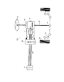
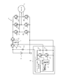
- FIGS. 1 to 3 a first embodiment will be described with reference to FIGS. 1 to 3. Note that the same parts as those in FIG. In FIG. 3 showing the overall configuration of the power steering apparatus 100, one end of the steering shaft 22 is fixed to a steering handle 21 disposed in the vehicle interior, and the rotational force of the rack shaft is driven by a rack and pinion mechanism 23. It is transmitted as a force that changes the direction of the wheel 25 attached to both ends via the connecting mechanism 24.
- the three-phase brushless DC motor 3 for assisting the rotational force is disposed on the steering shaft 22, and the motor 3 and the shaft 22 are connected via a speed reduction mechanism 26.
- the power supply voltage of the battery 4 is supplied to the motor drive control unit 28 via the wires 27a and 27b.
- the motor drive control unit 28 is disposed adjacent to or close to the vicinity of the motor 3, and performs PWM control of energization of the motor 3.
- a battery voltage is supplied to the motor drive control unit 28 as a control power source via the wiring 27, and the signal line 30 of the torque sensor 29 for detecting the torque applied to the steering shaft 22 and the rotational position of the motor 3 are set.
- a signal line 32 of a resolver 31 to be detected is connected.
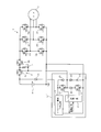
- FIG. 2 is a functional block diagram showing the internal configuration of the motor drive control unit 28.
- the current detector 33 (for example, a resistance element) is connected between the negative terminal (reference potential point) of the battery 4 and the negative DC bus of the inverter circuit 1, and the current signal obtained by the current detector 33 is The signal is input to the A / D conversion circuit 34.
- the current detection circuit 33 may be a current probe that detects a current by detecting a magnetic field generated by the current.
- the A / D conversion circuit 34 outputs data obtained by A / D converting the input current signal to the MCU 35.
- a steering angle signal from the torque sensor 29 and a steering angle signal from the resolver 31 are given to the input I / F (interface) circuit 36, and the input I / F circuit 36 responds to each input signal.
- a voltage signal is input to the MCU 35.
- the MCU 35 is configured by a microcomputer or the like, generates a gate signal for controlling each FET 2 constituting the inverter circuit 1 according to each input signal, and outputs the gate signal to the bridge gate drive circuit 37.
- the MCU 35 outputs a drive signal to the switch circuit 5 via the switch drive circuit 38.
- the MCU 35 When the power is supplied, the MCU 35 first outputs a shut-off command (OFF) signal to the switch circuit 5, and outputs a closing (ON) signal to the switch circuit 5 when its initialization process is completed. Thereby, the electric power of the battery 4 is supplied to the inverter circuit 1.
- the MCU 35 takes in the steering torque signal and the steering rotation speed, determines whether or not it is necessary to supply the steering assist force (torque) from the motor 3, and if so, based on the steering torque and the steering rotation speed. Thus, the rotation direction of the motor 3 and the steering assist force supplied from the motor 3 are obtained. Then, the MCU 35 generates and outputs a gate drive control signal based on the obtained rotation direction and steering assist force. Further, the MCU 35 outputs a cutoff command signal to the switch circuit 5 when the current value detected by the current detector 33 exceeds the overcurrent value.
- the bridge gate drive circuit 37 includes a booster circuit for generating a gate supply voltage for controlling the FETs 2U to 2W on the upper arm side constituting the inverter circuit 1 to a conductive state, and a plurality of level shift circuits (both shown in FIG. Not shown).
- the gate drive circuit 37 supplies a gate voltage signal to the gate of each FET 2 based on the gate drive control signal output from the MCU 35.
- the MCU 35 monitors the current flowing through the inverter circuit 1 based on the current value signal. When the current flowing through the inverter circuit 1 exceeds a preset allowable current, the MCU 35 stops driving the motor 3 and sends it to the switch circuit 5. Is turned off to cut off the power supply to the inverter circuit 1.
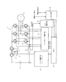
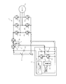
- FIG. 1 is a diagram corresponding to FIG. 6 showing the internal configuration of the switch drive circuit 38.
- the circuit ground is directly connected to the negative DC bus of the inverter circuit 1, but in the switch drive circuit 38 of the present embodiment, the forward diode 39 (current element diode). Is inserted between the two. Thereby, even when the battery 4 is connected with a reverse polarity as shown in FIG. 7, it is possible to prevent an overcurrent from flowing through the circuit via the parasitic diode of the FET 2.
- the switch drive circuit 38 has two N-channel MOSFETs 6a and 6b (N-channel semiconductor switching elements) so as to electrically open and close between the battery 4 and the inverter circuit 1.
- MOSFETs 6a and 6b N-channel semiconductor switching elements
- the reference potential point is shared with the inverter circuit 1 and an open / close control signal is output to the switch circuit 5.
- a half bridge circuit in which two N-channel MOSFETs 10 and 11 (semiconductor switching elements) are connected in series is provided between the power supply generation circuit 9 and the reference potential point. These FETs 10 and 11 are connected in parallel, respectively.
- the switch circuit 5 that can be configured more compactly than a relay for high power, and the power steering device 100 can be downsized. Even when the battery 4 is connected in reverse polarity, the reverse current is prevented from flowing by the parasitic diode of the FET 2 and the protective diode 14 in the switch drive circuit 38 to protect the inverter circuit 1 and the motor 3, and short circuit failure Can be prevented.
- FIG. 4 shows a second embodiment.
- the same parts as those in the first embodiment are denoted by the same reference numerals and the description thereof is omitted. Hereinafter, different parts will be described.
- a current blocking diode 42 instead of the diode 39, a current blocking diode 42, between the source of the N-channel MOSFET 11 and the circuit ground, and between the anode of the protection diode 14 and the circuit ground, respectively. 43 is inserted.
- the second embodiment configured as described above, the same effect as that of the first embodiment can be obtained.
- FIG. 5 shows a third embodiment, and the differences from the second embodiment will be described.
- the switch drive circuit 41 ′ of the third embodiment includes the current blocking diodes 42 and 43 of the second embodiment between the source of the N-channel MOSFET 10 and the drain of the N-channel MOSFET 11, the anode of the protection diode 13, and the protection diode 14. It is the structure arrange
- a P-channel MOSFET may be used instead of the N-channel MOSFET 10. Further, a P-channel MOSFET may be used for the upper arm of the inverter circuit 1.
- the present invention is not limited to a power steering device, and any device having a switch circuit configured using an N-channel semiconductor switching element between a DC power source and an inverter circuit is applicable.
- the switch drive circuit according to the embodiment of the present invention is configured by connecting two N-channel type semiconductor switching elements in series in the reverse direction in order to electrically open and close between the DC power supply and the inverter circuit. This is useful for opening and closing a switch circuit.
Landscapes
- Engineering & Computer Science (AREA)
- Power Engineering (AREA)
- Inverter Devices (AREA)
- Power Steering Mechanism (AREA)
- Physics & Mathematics (AREA)
- Ceramic Engineering (AREA)
- Condensed Matter Physics & Semiconductors (AREA)
- General Physics & Mathematics (AREA)
- Microelectronics & Electronic Packaging (AREA)
Abstract
本発明の実施形態におけるスイッチ駆動回路(38)は、直流電源(4)とインバータ回路(1)との間を電気的に開閉するように、2つのNチャネル型半導体スイッチング素子(6a,6b)を逆方向に直列接続して構成されるスイッチ回路(5)を開閉させるため、基準電位点を前記インバータ回路と共通にしてスイッチ回路に開閉制御信号を出力するもので、駆動用電源と基準電位点との間に2つの半導体スイッチング素子(10,11)を直列接続したハーフブリッジ回路を有し、2つの半導体スイッチング素子(10,11)にはそれぞれ並列に保護用ダイオード(13,14)が接続され、直流電源がインバータ回路に対して逆極性で接続された場合、基準電位点より自身を経由してスイッチ回路側に流出しようとする電流を阻止するダイオード(39,42,43)を備える。
Description
本発明の実施形態は、直流電源とインバータ回路との間を電気的に開閉するためのスイッチ回路に開閉制御信号を出力するスイッチ駆動回路,及び前記インバータ回路及びスイッチング駆動回路を備えてなるインバータ装置,並びに前記インバータ装置を備えてなるパワーステアリング装置に関する。
電動パワーステアリング装置は、ドライバの操作によりハンドルを介して与えられる操舵入力トルクを操舵トルクセンサで検知し、操舵トルクセンサの出力信号に基づき制御装置においてモータの出力の大きさと方向とを決定すると、インバータ回路を介してモータを駆動し、そのモータの動力をステアリング系に伝達して操舵トルクの軽減を図るものである。
従来の電動パワーステアリング装置では、電源であるバッテリとインバータ回路との間にリレーを用いて構成した開閉器を挿入し、制御装置は、過電流状態やPWM制御の異常を検出すると、開閉器を開いてインバータ回路,モータへの給電を遮断し、モータから所望しない補助操舵力が発生するのを防止している。しかしながら、リレーを用いて構成した開閉器は、操舵補助トルクを発生させるために数10A~100A程度の大電流をモータへ供給する必要があるが、このような大電流を開閉できるリレーは大型であるため、電動パワーステアリング装置が大型になる。そこで、リレーの代わりにFETなどの半導体スイッチング素子を用いたスイッチ回路を用いることが考えられている。
特開2004-168124号公報
特開平10-167085号公報
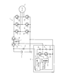
この場合に想定される構成の一例を図6に示す。インバータ回路1は、6個のパワーMOSFET(Nチャネル)2(U~W,X~Z)を三相ブリッジ接続して構成されており、各相出力端子には、モータ3の各相巻線(図示せず)が接続されている。モータ3は、例えばブラシレスDCモータである。車両のバッテリ4の正側端子は、スイッチ回路5を介してインバータ回路1の正側直流母線に接続されており、負側端子(ボディアース)は、負側直流母線に接続されている。
スイッチ回路5は、2つのNチャネルMOSFET6a,6bを、互いのソースを共通に接続して構成され、NチャネルMOSFET6aのドレインがバッテリ4の正側端子に接続されており、NチャネルMOSFET6aのドレインがインバータ回路1の正側直流母線に接続されている。双方のゲートは共通に接続され、ソースとの間には抵抗素子7が接続されている。
スイッチ回路5を駆動する駆動回路8は、インバータ回路1を制御するICであるMCU(Micro Control Unit;マイクロコンピュータ)などの周辺回路として構成されており、その電源はバッテリ4からダイオード15を介して直接供給されており、回路グランドはインバータ回路1の負側直流母線に接続されている。そして、スイッチ回路5を駆動するための駆動用電源を生成する電源生成回路9の出力端子とグランドとの間には、2つのNチャネルMOSFET10及び11の直列回路が接続されている。これらのFET10及び11のゲートには、上記MCUより出力される駆動信号がハーフブリッジ(H/B)駆動回路12を介して個別に出力される。また、NチャネルMOSFET10及び11には、保護用のダイオード13及び14がそれぞれ並列に接続されている。
MOSFET10及び11の共通接続点(ソース及びドレイン)は、スイッチ回路5を構成するNチャネルMOSFET6a,6bのゲートに接続されている。H/B駆動回路12は、MCUからの駆動信号に応じてスイッチ回路5をオンする場合には、NチャネルMOSFET10をオン,NチャネルMOSFET11をオフしてNチャネルMOSFET6a,6bのゲート電位をハイレベルにする。また、スイッチ回路5をオフする場合には、NチャネルMOSFET10をオフ,NチャネルMOSFET11をオンしてNチャネルMOSFET6a,6bのゲート電位をローレベルにする。
以上のように車両に搭載されてバッテリ4より電源供給を受ける装置については、バッテリ4が逆方向に接続された場合に回路が保護されるかどうかを検討する必要がある。そこで、図6に示す構成について、バッテリ4が逆方向に接続された場合を想定すると、以下のような問題がある。このとき、図7に示すように、インバータ回路1の負側直流母線の電位が上昇するため、以下の経路で電圧が印加される。
バッテリ4の正側端子-負側直流母線→ダイオード14(又はFET11のボディダイオード)→スイッチ回路5(FET6aのゲート-ドレイン)→バッテリ4の負側端子
これにより、スイッチ回路5のFET6において、ゲート-ソース間に閾値を超える電位差が印加されるため、スイッチ回路5がオンして上記の電圧印加経路に沿って電流が流れる。同時に、FET6b側がオンすると、インバータ回路1を構成するFET2U,2Xのボディダイオードを経由しても電流が流れる。この時に流れるバッテリ4の短絡電流によって経路中の各素子が破壊される虞がある。
これにより、スイッチ回路5のFET6において、ゲート-ソース間に閾値を超える電位差が印加されるため、スイッチ回路5がオンして上記の電圧印加経路に沿って電流が流れる。同時に、FET6b側がオンすると、インバータ回路1を構成するFET2U,2Xのボディダイオードを経由しても電流が流れる。この時に流れるバッテリ4の短絡電流によって経路中の各素子が破壊される虞がある。
尚、スイッチ回路については、図8に示すように、スイッチング素子の一方にPチャネルMOSFET16を用い、互いの寄生ダイオードのアノードが共通となるように接続することも考えられ、この場合には、上記のような逆流の問題が発生しない。しかし、PチャネルMOSFETの素子サイズはNチャネルMOSFETに比較すると大きく、また、それぞれのFETに異なるレベルのゲート信号を与えて制御する必要があることから、一般には図6に示すようにNチャネル同士の組み合わせで構成されることが多い。したがって、上記の問題に対処する必要がある。
そこで、バッテリが逆方向に接続された場合でも、回路素子を確実に保護できるスイッチ駆動回路,インバータ装置及びパワーステアリング装置を提供する。
実施形態によれば、スイッチ駆動回路は、直流電源とインバータ回路との間を電気的に開閉するように、2つのNチャネル型半導体スイッチング素子を逆方向に直列接続して構成されるスイッチ回路を開閉させるため、基準電位点を前記インバータ回路と共通にして前記スイッチ回路に開閉制御信号を出力する。スイッチ駆動回路は、駆動用電源と前記基準電位点との間に、2つの半導体スイッチング素子を直列接続したハーフブリッジ回路を有し、前記2つの半導体スイッチング素子には、それぞれ並列に保護用ダイオードが接続され、前記直流電源が前記インバータ回路に対して逆極性で接続された場合に、前記基準電位点より、自身を経由して前記スイッチ回路側に流出しようとする電流を阻止するための電流阻止用ダイオードを備えている。
また、実施形態によれば、インバータ装置は、直流電源が供給されるインバータ回路と、前記直流電源と前記インバータ回路との間を電気的に開閉するスイッチ回路と、
基準電位点を前記インバータ回路と共通にして、前記スイッチ回路の開閉を制御する信号を出力するスイッチ駆動回路とを備える。前記スイッチ回路は、2つのNチャネル型半導体スイッチング素子を逆方向に直列接続して構成され、前記スイッチ駆動回路は、駆動用電源と前記基準電位点との間に、2つの半導体スイッチング素子を直列接続したハーフブリッジ回路を有しており、前記2つの半導体スイッチング素子には、それぞれ並列に保護用ダイオードが接続されている。そして、前記直流電源が前記インバータ回路に対して逆極性で接続された場合に、前記基準電位点より、自身を経由して前記スイッチ回路側に流出しようとする電流を阻止するための電流阻止用ダイオードを備えている。
基準電位点を前記インバータ回路と共通にして、前記スイッチ回路の開閉を制御する信号を出力するスイッチ駆動回路とを備える。前記スイッチ回路は、2つのNチャネル型半導体スイッチング素子を逆方向に直列接続して構成され、前記スイッチ駆動回路は、駆動用電源と前記基準電位点との間に、2つの半導体スイッチング素子を直列接続したハーフブリッジ回路を有しており、前記2つの半導体スイッチング素子には、それぞれ並列に保護用ダイオードが接続されている。そして、前記直流電源が前記インバータ回路に対して逆極性で接続された場合に、前記基準電位点より、自身を経由して前記スイッチ回路側に流出しようとする電流を阻止するための電流阻止用ダイオードを備えている。
また、実施形態によれば、パワーステアリング装置は、車両のステアリングの操舵力を補助する補助操舵力を発生させるモータと、このモータを制御する請求項5ないし8の何れかに記載のインバータ装置とを備える。
本発明のインバータ装置は、半導体スイッチング素子を用いることにより、大電力用のリレーと比較して小形に構成できるスイッチ回路5を用いることができ、パワーステアリング装置100の小型化を図ることができる。また、バッテリ4が逆極性に接続された場合でも、FET2の寄生ダイオードとスイッチ駆動回路38内の保護ダイオード14により逆電流が流れることを阻止してインバータ回路1やモータ3を保護し、短絡故障を防止することができる。
1はインバータ回路、3はモータ、4はバッテリ(直流電源)、5はスイッチ駆動回路、6はNチャネルMOSFET(Nチャネル型半導体スイッチング素子)、10及び11はNチャネルMOSFET(半導体スイッチング素子)、13,14は保護用ダイオード、38はスイッチ駆動回路、39は電流阻止用ダイオード、41はスイッチ駆動回路、42,43は電流阻止用ダイオード、100はパワーステアリング装置を示す。
(第1実施形態)
以下、第1実施形態について図1ないし図3を参照して説明する。尚、図6と同一部分には同一符号を付して説明を省略し、以下異なる部分について説明する。パワーステアリング装置100全体の構成を示す図3において、ステアリングシャフト22は、車室内に配置されている操舵ハンドル21に一端が固定されており、その回転力は、ラックピニオン機構23により、ラック軸の両端に連結機構24を介して取り付けられた車輪25の方向を変える力として伝達される。回転力を補助するための三相のブラシレスDCモータ3は、ステアリングシャフト22に配置されており、モータ3とシャフト22とは減速機構26を介して連結されている。
以下、第1実施形態について図1ないし図3を参照して説明する。尚、図6と同一部分には同一符号を付して説明を省略し、以下異なる部分について説明する。パワーステアリング装置100全体の構成を示す図3において、ステアリングシャフト22は、車室内に配置されている操舵ハンドル21に一端が固定されており、その回転力は、ラックピニオン機構23により、ラック軸の両端に連結機構24を介して取り付けられた車輪25の方向を変える力として伝達される。回転力を補助するための三相のブラシレスDCモータ3は、ステアリングシャフト22に配置されており、モータ3とシャフト22とは減速機構26を介して連結されている。
バッテリ4の電源電圧は、配線27a,27bを経由してモータ駆動制御部28に供給される。モータ駆動制御部28は、モータ3の近傍に隣接または密着して配置されており、モータ3に対する通電をPWM制御する。モータ駆動制御部28には、制御電源用としてバッテリ電圧が配線27を介して供給されると共に、ステアリングシャフト22に加えられるトルクを検出するトルクセンサ29の信号線30や、モータ3の回転位置を検出するレゾルバ31の信号線32が接続されている。
図2は、モータ駆動制御部28の内部構成を示す機能ブロック図である。電流検出器33(例えば抵抗素子)は、バッテリ4の負側端子(基準電位点)とインバータ回路1の負側直流母線との間に接続されており、電流検出器33によって得られる電流信号はA/D変換回路34に入力されている。尚、電流検出回路33には、電流によって発生する磁界を検出することで電流を検出する電流プローブを用いても良い。A/D変換回路34は、入力された電流信号をA/D変換したデータをMCU35に出力する。
入力I/F(インターフェイス)回路36には、トルクセンサ29からの操舵角度信号と、レゾルバ31からの操舵角信号とが与えられており、入力I/F回路36は、各入力信号に応じた電圧信号をMCU35に入力する。MCU35は、マイクロコンピュータ等で構成されており、各入力信号に応じてインバータ回路1を構成する各FET2を制御するためのゲート信号を生成してブリッジ用ゲート駆動回路37に出力する。また、MCU35は、スイッチ駆動回路38を介してスイッチ回路5に駆動信号を出力する。そして、これらの各回路には、図示しない車両のイグニッションスイッチがオンされると、バッテリ4からの電源が供給される。
MCU35は、電源が供給されると先ずスイッチ回路5に遮断指令(OFF)信号を出力し、自身の初期化処理が終了するとスイッチ回路5に閉路(ON)信号を出力する。これによりバッテリ4の電力がインバータ回路1に供給される。MCU35は、操舵トルク信号,操舵回転速度を取り込み、モータ3から操舵補助力(トルク)を供給する必要があるか否かを判断し、供給する必要がある場合は操舵トルク,操舵回転速度に基づいてモータ3の回転方向並びにモータ3から供給する操舵補助力を求める。そして、MCU35は、求めた回転方向及び操舵補助力に基づいてゲート駆動制御信号を生成して出力する。また、MCU35は、電流検出器33で検出した電流値が過電流値を超えるとスイッチ回路5に遮断指令信号を出力する。
ブリッジ用ゲート駆動回路37は、インバータ回路1を構成する上アーム側のFET2U~2Wを導通状態に制御するためのゲート供給電圧を発生する昇圧回路と、複数のレベルシフト回路を備える(何れも図示せず)。ゲート駆動回路37は、MCU35から出力されるゲート駆動制御信号に基づいて各FET2のゲートにゲート電圧信号を供給する。MCU35は、電流値信号に基づいてインバータ回路1を流れる電流を監視しており、インバータ回路1を流れる電流が予め設定した許容電流を超えると、モータ3の駆動を停止すると共に、スイッチ回路5への通電を遮断してインバータ回路1への給電を遮断する。
図1は、スイッチ駆動回路38の内部構成を示す図6相当図である。図6に示す駆動回路8では、その回路グランドはインバータ回路1の負側直流母線に直接接続されていたが、本実施形態のスイッチ駆動回路38では、順方向のダイオード39(電流素子用ダイオード)が両者の間に挿入されている。これにより、図7に示したようにバッテリ4が逆極性で接続された場合でも、FET2の寄生ダイオードを介して回路に過電流が流れることが防止される。
以上のように本実施形態によれば、スイッチ駆動回路38は、バッテリ4とインバータ回路1との間を電気的に開閉するように、2つのNチャネルMOSFET6a,6b(Nチャネル型半導体スイッチング素子)を逆方向に直列接続して構成されるスイッチ回路5を開閉させるため、基準電位点をインバータ回路1と共通にしてスイッチ回路5に開閉制御信号を出力する。そして、電源生成回路9と前記基準電位点との間に、2つのNチャネルMOSFET10及び11(半導体スイッチング素子)を直列接続したハーフブリッジ回路を有し、これらのFET10及び11には、それぞれ並列に保護用ダイオード13,14を接続し、バッテリ4がインバータ回路1に対して逆極性で接続された場合に、基準電位点より、自身を経由してスイッチ回路5側に流出しようとする電流を阻止するためのダイオード39を備えた。
したがって、大電力用のリレーと比較して小形に構成できるスイッチ回路5を用いることができ、パワーステアリング装置100の小型化を図ることができる。そして、バッテリ4が逆極性に接続された場合でも、FET2の寄生ダイオードとスイッチ駆動回路38内の保護ダイオード14により逆電流が流れることを阻止してインバータ回路1やモータ3を保護し、短絡故障を防止することができる。
(第2実施形態)
図4は第2実施形態であり、第1実施形態と同一部分には同一符号を付して説明を省略し、以下異なる部分について説明する。第2実施形態のスイッチ駆動回路41は、ダイオード39に替えて、NチャネルMOSFET11のソースと回路グランドとの間,保護ダイオード14のアノードと回路グランドとの間に、それぞれ電流阻止用のダイオード42,43を挿入した構成である。このように構成した第2実施形態による場合も、第1実施形態と同様の効果が得られる。
図4は第2実施形態であり、第1実施形態と同一部分には同一符号を付して説明を省略し、以下異なる部分について説明する。第2実施形態のスイッチ駆動回路41は、ダイオード39に替えて、NチャネルMOSFET11のソースと回路グランドとの間,保護ダイオード14のアノードと回路グランドとの間に、それぞれ電流阻止用のダイオード42,43を挿入した構成である。このように構成した第2実施形態による場合も、第1実施形態と同様の効果が得られる。
(第3実施形態)
図5は第3実施形態であり、第2実施形態と異なる部分について説明する。第3実施形態のスイッチ駆動回路41’は、第2実施形態の電流阻止用ダイオード42,43を、NチャネルMOSFET10のソースとNチャネルMOSFET11のドレインとの間、保護ダイオード13のアノードと保護ダイオード14のカソードとの間に配置した構成である。このように構成した第3実施形態による場合も、第1,第2実施形態と同様の効果が得られる。
図5は第3実施形態であり、第2実施形態と異なる部分について説明する。第3実施形態のスイッチ駆動回路41’は、第2実施形態の電流阻止用ダイオード42,43を、NチャネルMOSFET10のソースとNチャネルMOSFET11のドレインとの間、保護ダイオード13のアノードと保護ダイオード14のカソードとの間に配置した構成である。このように構成した第3実施形態による場合も、第1,第2実施形態と同様の効果が得られる。
本発明のいくつかの実施形態を説明したが、これらの実施形態は例として提示したものであり、発明の範囲を限定することは意図していない。これら新規な実施形態は、その他の様々な形態で実施されることが可能であり、発明の要旨を逸脱しない範囲で種々の省略、置き換え、変更を行うことができる。これら実施形態やその変形は、発明の範囲や要旨に含まれると共に、特許請求の範囲に記載された発明とその均等の範囲に含まれる。
NチャネルMOSFET10に替えてPチャネルMOSFETを用いても良い。また、インバータ回路1の上アームにPチャネルMOSFETを用いても良い。
パワーステアリング装置に限ることなく、直流電源とインバータ回路との間にNチャネル型半導体スイッチング素子を用いて構成されるスイッチ回路を備えるものであれば適用が可能である。
以上のように、本発明の実施形態にかかるスイッチ駆動回路は、直流電源とインバータ回との間を電気的に開閉するため、2つのNチャネル型半導体スイッチング素子を逆方向に直列接続して構成されるスイッチ回路を開閉させるものに有用である。
Claims (9)
- 直流電源(4)とインバータ回路(1)との間を電気的に開閉するように、2つのNチャネル型半導体スイッチング素子(6a,6b)を逆方向に直列接続して構成されるスイッチ回路(5)を開閉させるため、基準電位点を前記インバータ回路と共通にして、前記スイッチ回路に開閉制御信号を出力するスイッチ駆動回路(38)において、
駆動用電源と前記基準電位点との間に、2つの半導体スイッチング素子(10,11)を直列接続したハーフブリッジ回路を有し、
前記2つの半導体スイッチング素子(10,11)には、それぞれ並列に保護用ダイオード(13,14)が接続され、
前記直流電源(4)が、前記インバータ回路(1)に対して逆極性で接続された場合に、前記基準電位点より、自身を経由して前記スイッチ回路(5)側に流出しようとする電流を阻止するための電流阻止用ダイオード(39,42,43)を備えていることを特徴とするスイッチ駆動回路。 - 請求項1記載のスイッチ駆動回路において、
前記電流阻止用ダイオード(42,43)は、前記ハーフブリッジ回路の信号出力端子と、基準電位側の半導体スイッチング素子(11)との間,及び前記半導体スイッチング素子(11)に並列に接続される保護用ダイオード(14)との間にそれぞれ接続されている。 - 請求項1記載のスイッチ駆動回路において、
前記電流阻止用ダイオード(42,43)は、前記基準電位側の半導体スイッチング素子(11),及び前記半導体スイッチング素子に並列に接続される保護用ダイオード(14)と、前記前記基準電位点との間にそれぞれ接続されている。 - 請求項1記載のスイッチ駆動回路において、
前記電流阻止用ダイオード(39)は、前記基準電位側の半導体スイッチング素子(11),及び前記半導体スイッチング素子(11)に並列に接続される保護用ダイオード(14)と、前記前記基準電位点とを接続する配線間に1つだけ接続されている。 - 直流電源(4)が供給されるインバータ回路(1)と、
前記直流電源(4)と前記インバータ回路(1)との間を電気的に開閉するスイッチ回路(5)と、
基準電位点を前記インバータ回路(1)と共通にして、前記スイッチ回路(5)の開閉を制御する信号を出力するスイッチ駆動回路(38)とを備え、
前記スイッチ回路(5)は、2つのNチャネル型半導体スイッチング素子(6a,6b)を逆方向に直列接続して構成され、
前記スイッチ駆動回路(38)は、
駆動用電源と前記基準電位点との間に、2つの半導体スイッチング素子(10,11)を直列接続したハーフブリッジ回路を有しており、前記2つの半導体スイッチング素子(10,11)には、それぞれ並列に保護用ダイオード(13,14)が接続され、
前記直流電源(4)が、前記インバータ回路(1)に対して逆極性で接続された場合に、前記基準電位点より、自身を経由して前記スイッチ回路(5)側に流出しようとする電流を阻止するための電流阻止用ダイオード(39,42,43)を備えていることを特徴とするインバータ装置。 - 請求項5記載のインバータ装置において、
前記電流阻止用ダイオード(42,43)は、前記ハーフブリッジ回路の信号出力端子と、基準電位側の半導体スイッチング素子(11)との間,及び前記半導体スイッチング素子(11)に並列に接続される保護用ダイオード(14)との間にそれぞれ接続されている。 - 請求項5記載のインバータ装置において、
前記電流阻止用ダイオード(42,43)は、前記基準電位側の半導体スイッチング素子(11),及び前記半導体スイッチング素子(11)に並列に接続される保護用ダイオード(14)と、前記前記基準電位点との間にそれぞれ接続されている。 - 請求項5記載のインバータ装置において、
前記電流阻止用ダイオード(39)は、前記基準電位側の半導体スイッチング素子(11),及び前記半導体スイッチング素子(11)に並列に接続される保護用ダイオード(14)と、前記前記基準電位点とを接続する配線間に1つだけ接続されている。 - 車両のステアリング(21)の操舵力を補助する補助操舵力を発生させるモータ(3)と、
このモータを制御する請求項5ないし8の何れかに記載のインバータ装置とを備えることを特徴とするパワーステアリング装置。
Priority Applications (4)
| Application Number | Priority Date | Filing Date | Title |
|---|---|---|---|
| EP12830399.7A EP2755314B1 (en) | 2011-09-07 | 2012-08-10 | Switch driving circuit, inverter apparatus and power steering apparatus |
| CN201280041766.3A CN103782469B (zh) | 2011-09-07 | 2012-08-10 | 开关驱动电路、逆变器装置以及动力转向装置 |
| KR1020147008758A KR101711711B1 (ko) | 2011-09-07 | 2012-08-10 | 스위치 구동 회로, 인버터 장치 및 파워 스티어링 장치 |
| US14/200,858 US9564485B2 (en) | 2011-09-07 | 2014-03-07 | Switch driving circuit, inverter apparatus and power steering apparatus |
Applications Claiming Priority (2)
| Application Number | Priority Date | Filing Date | Title |
|---|---|---|---|
| JP2011-195051 | 2011-09-07 | ||
| JP2011195051A JP5638488B2 (ja) | 2011-09-07 | 2011-09-07 | スイッチ駆動回路,インバータ装置及びパワーステアリング装置 |
Related Child Applications (1)
| Application Number | Title | Priority Date | Filing Date |
|---|---|---|---|
| US14/200,858 Continuation US9564485B2 (en) | 2011-09-07 | 2014-03-07 | Switch driving circuit, inverter apparatus and power steering apparatus |
Publications (1)
| Publication Number | Publication Date |
|---|---|
| WO2013035491A1 true WO2013035491A1 (ja) | 2013-03-14 |
Family
ID=47831942
Family Applications (1)
| Application Number | Title | Priority Date | Filing Date |
|---|---|---|---|
| PCT/JP2012/070504 Ceased WO2013035491A1 (ja) | 2011-09-07 | 2012-08-10 | スイッチ駆動回路,インバータ装置及びパワーステアリング装置 |
Country Status (6)
| Country | Link |
|---|---|
| US (1) | US9564485B2 (ja) |
| EP (1) | EP2755314B1 (ja) |
| JP (1) | JP5638488B2 (ja) |
| KR (1) | KR101711711B1 (ja) |
| CN (1) | CN103782469B (ja) |
| WO (1) | WO2013035491A1 (ja) |
Families Citing this family (16)
| Publication number | Priority date | Publication date | Assignee | Title |
|---|---|---|---|---|
| JP5638488B2 (ja) * | 2011-09-07 | 2014-12-10 | 株式会社東芝 | スイッチ駆動回路,インバータ装置及びパワーステアリング装置 |
| WO2015145733A1 (ja) | 2014-03-28 | 2015-10-01 | 三菱電機株式会社 | 車載機器 |
| EP3041103A1 (en) * | 2014-12-29 | 2016-07-06 | Rockwell Automation Limited | Circuit protection |
| KR20170028133A (ko) | 2015-09-03 | 2017-03-13 | 주식회사 만도 | 방열 구조가 개선된 인버터 어셈블리 |
| GB2555117B (en) * | 2016-10-18 | 2022-03-02 | Trw Ltd | A motor drive circuit |
| GB2557295B (en) * | 2016-12-05 | 2022-07-20 | Trw Ltd | Control for electric power steering |
| JP6613256B2 (ja) * | 2017-03-13 | 2019-11-27 | ミネベアミツミ株式会社 | 保護回路及び負荷駆動回路 |
| US20180302017A1 (en) * | 2017-04-12 | 2018-10-18 | Power Integrations, Inc. | Current sense circuit for a dc motor inverter |
| JP6903597B2 (ja) * | 2018-01-31 | 2021-07-14 | ミネベアミツミ株式会社 | 負荷駆動回路 |
| KR102502388B1 (ko) * | 2018-06-19 | 2023-02-23 | 에이치엘만도 주식회사 | 차량의 eps 전원 공급 제어 장치 및 방법 |
| FR3083770B1 (fr) * | 2018-07-10 | 2020-06-19 | Jtekt Europe | Procede de controle d’un systeme de direction avec deux motorisations redondantes |
| KR102434048B1 (ko) * | 2018-07-26 | 2022-08-19 | 현대모비스 주식회사 | 전자식 릴레이 장치 |
| DE102020103190A1 (de) * | 2019-02-08 | 2020-08-13 | Steering Solutions Ip Holding Corporation | Halbleiter-motordämpfung |
| WO2022056797A1 (en) * | 2020-09-18 | 2022-03-24 | Techtronic Cordless Gp | Motor driven appliance and protection method thereof |
| GB2601532B (en) * | 2020-12-03 | 2024-06-12 | Dyson Technology Ltd | Gate driver |
| DE102021125556A1 (de) * | 2021-10-01 | 2023-04-06 | HELLA GmbH & Co. KGaA | Batteriemanagementsystem für einen Batteriespeicher, Anordnung und Verfahren |
Citations (3)
| Publication number | Priority date | Publication date | Assignee | Title |
|---|---|---|---|---|
| JP2004168124A (ja) * | 2002-11-19 | 2004-06-17 | Nissan Motor Co Ltd | ブレーキ制御装置 |
| JP2009274686A (ja) * | 2008-05-19 | 2009-11-26 | Nsk Ltd | 電動パワーステアリング装置 |
| JP2010259245A (ja) * | 2009-04-27 | 2010-11-11 | Yaskawa Electric Corp | 出力フィルタおよび電力変換装置 |
Family Cites Families (12)
| Publication number | Priority date | Publication date | Assignee | Title |
|---|---|---|---|---|
| DE3835662A1 (de) * | 1988-10-20 | 1990-04-26 | Daimler Benz Ag | Vorrichtung zur ansteuerung induktiver verbraucher in einem kraftfahrzeug |
| JP3375502B2 (ja) | 1996-12-12 | 2003-02-10 | 本田技研工業株式会社 | 電動パワーステアリング装置 |
| JP3698550B2 (ja) * | 1998-07-02 | 2005-09-21 | 富士通株式会社 | ブースト回路及びこれを用いた半導体装置 |
| IL134628A0 (en) * | 2000-02-20 | 2001-04-30 | Elisra Electronic Systems Ltd | Electronic circuit breaker |
| FR2851698B1 (fr) * | 2003-02-21 | 2005-08-19 | Valeo Systemes Dessuyage | Circuit de commande d'un moteur electrique a courant continu et systeme d'essuyage utilisant un tel circuit |
| DE102004007991B4 (de) * | 2004-02-18 | 2015-07-30 | Infineon Technologies Ag | Halbleiter-Schaltelement |
| CN200983560Y (zh) * | 2006-09-05 | 2007-11-28 | 任文华 | 一种组合式开关及电源装置 |
| DE102008016589A1 (de) * | 2008-03-31 | 2009-10-01 | Weidmüller Interface GmbH & Co. KG | Schutzvorrichtung |
| JP2010074915A (ja) | 2008-09-17 | 2010-04-02 | Jtekt Corp | モータ制御装置及び電動パワーステアリング装置 |
| JP5246407B2 (ja) * | 2008-11-04 | 2013-07-24 | 株式会社ジェイテクト | モータ駆動回路及び電動パワーステアリング装置 |
| CN201717802U (zh) * | 2010-07-05 | 2011-01-19 | 常熟开关制造有限公司(原常熟开关厂) | 一种防反接逆变电路 |
| JP5638488B2 (ja) * | 2011-09-07 | 2014-12-10 | 株式会社東芝 | スイッチ駆動回路,インバータ装置及びパワーステアリング装置 |
-
2011
- 2011-09-07 JP JP2011195051A patent/JP5638488B2/ja active Active
-
2012
- 2012-08-10 EP EP12830399.7A patent/EP2755314B1/en active Active
- 2012-08-10 WO PCT/JP2012/070504 patent/WO2013035491A1/ja not_active Ceased
- 2012-08-10 KR KR1020147008758A patent/KR101711711B1/ko active Active
- 2012-08-10 CN CN201280041766.3A patent/CN103782469B/zh active Active
-
2014
- 2014-03-07 US US14/200,858 patent/US9564485B2/en active Active
Patent Citations (3)
| Publication number | Priority date | Publication date | Assignee | Title |
|---|---|---|---|---|
| JP2004168124A (ja) * | 2002-11-19 | 2004-06-17 | Nissan Motor Co Ltd | ブレーキ制御装置 |
| JP2009274686A (ja) * | 2008-05-19 | 2009-11-26 | Nsk Ltd | 電動パワーステアリング装置 |
| JP2010259245A (ja) * | 2009-04-27 | 2010-11-11 | Yaskawa Electric Corp | 出力フィルタおよび電力変換装置 |
Also Published As
| Publication number | Publication date |
|---|---|
| US20140184107A1 (en) | 2014-07-03 |
| EP2755314A1 (en) | 2014-07-16 |
| EP2755314B1 (en) | 2020-10-21 |
| KR101711711B1 (ko) | 2017-03-02 |
| KR20140057380A (ko) | 2014-05-12 |
| US9564485B2 (en) | 2017-02-07 |
| CN103782469B (zh) | 2016-09-21 |
| JP5638488B2 (ja) | 2014-12-10 |
| JP2013059167A (ja) | 2013-03-28 |
| CN103782469A (zh) | 2014-05-07 |
| EP2755314A4 (en) | 2016-06-01 |
Similar Documents
| Publication | Publication Date | Title |
|---|---|---|
| JP5638488B2 (ja) | スイッチ駆動回路,インバータ装置及びパワーステアリング装置 | |
| JP5743934B2 (ja) | インバータ装置及びパワーステアリング装置 | |
| JP5532065B2 (ja) | 電動機駆動装置 | |
| CN101883706B (zh) | 电动动力转向装置 | |
| CN103359159B (zh) | 电机驱动装置 | |
| CN101883707B (zh) | 电动动力转向装置 | |
| KR101704112B1 (ko) | 모터 구동 장치 | |
| JP2011244611A (ja) | モータ駆動装置 | |
| JP2015171305A (ja) | 電源供給回路 | |
| JP2015165745A (ja) | 電源供給回路 | |
| JP6268140B2 (ja) | 電動モータ駆動回路 | |
| US10404202B2 (en) | Electronic control device and control method thereof | |
| JP7226533B2 (ja) | 電気機器 | |
| KR102313672B1 (ko) | 전동식 파워 스티어링 시스템의 모터 구동 회로 | |
| JP5660996B2 (ja) | 電動機制御装置 | |
| US9694695B2 (en) | Power source system | |
| WO2023026943A1 (ja) | 電力供給装置 | |
| JP5458954B2 (ja) | 電動パワーステアリング装置 |
Legal Events
| Date | Code | Title | Description |
|---|---|---|---|
| 121 | Ep: the epo has been informed by wipo that ep was designated in this application |
Ref document number: 12830399 Country of ref document: EP Kind code of ref document: A1 |
|
| NENP | Non-entry into the national phase |
Ref country code: DE |
|
| WWE | Wipo information: entry into national phase |
Ref document number: 2012830399 Country of ref document: EP |
|
| ENP | Entry into the national phase |
Ref document number: 20147008758 Country of ref document: KR Kind code of ref document: A |