WO2013038860A1 - 炭化珪素半導体装置およびその製造方法 - Google Patents
炭化珪素半導体装置およびその製造方法 Download PDFInfo
- Publication number
- WO2013038860A1 WO2013038860A1 PCT/JP2012/070658 JP2012070658W WO2013038860A1 WO 2013038860 A1 WO2013038860 A1 WO 2013038860A1 JP 2012070658 W JP2012070658 W JP 2012070658W WO 2013038860 A1 WO2013038860 A1 WO 2013038860A1
- Authority
- WO
- WIPO (PCT)
- Prior art keywords
- silicon carbide
- plane
- layer
- semiconductor device
- type
- Prior art date
- Legal status (The legal status is an assumption and is not a legal conclusion. Google has not performed a legal analysis and makes no representation as to the accuracy of the status listed.)
- Ceased
Links
Images












Classifications
-
- H—ELECTRICITY
- H10—SEMICONDUCTOR DEVICES; ELECTRIC SOLID-STATE DEVICES NOT OTHERWISE PROVIDED FOR
- H10D—INORGANIC ELECTRIC SEMICONDUCTOR DEVICES
- H10D62/00—Semiconductor bodies, or regions thereof, of devices having potential barriers
- H10D62/80—Semiconductor bodies, or regions thereof, of devices having potential barriers characterised by the materials
- H10D62/81—Semiconductor bodies, or regions thereof, of devices having potential barriers characterised by the materials of structures exhibiting quantum-confinement effects, e.g. single quantum wells; of structures having periodic or quasi-periodic potential variation
-
- H—ELECTRICITY
- H10—SEMICONDUCTOR DEVICES; ELECTRIC SOLID-STATE DEVICES NOT OTHERWISE PROVIDED FOR
- H10D—INORGANIC ELECTRIC SEMICONDUCTOR DEVICES
- H10D12/00—Bipolar devices controlled by the field effect, e.g. insulated-gate bipolar transistors [IGBT]
- H10D12/01—Manufacture or treatment
- H10D12/031—Manufacture or treatment of IGBTs
-
- H—ELECTRICITY
- H10—SEMICONDUCTOR DEVICES; ELECTRIC SOLID-STATE DEVICES NOT OTHERWISE PROVIDED FOR
- H10D—INORGANIC ELECTRIC SEMICONDUCTOR DEVICES
- H10D12/00—Bipolar devices controlled by the field effect, e.g. insulated-gate bipolar transistors [IGBT]
- H10D12/01—Manufacture or treatment
- H10D12/031—Manufacture or treatment of IGBTs
- H10D12/032—Manufacture or treatment of IGBTs of vertical IGBTs
- H10D12/038—Manufacture or treatment of IGBTs of vertical IGBTs having a recessed gate, e.g. trench-gate IGBTs
-
- H—ELECTRICITY
- H10—SEMICONDUCTOR DEVICES; ELECTRIC SOLID-STATE DEVICES NOT OTHERWISE PROVIDED FOR
- H10D—INORGANIC ELECTRIC SEMICONDUCTOR DEVICES
- H10D12/00—Bipolar devices controlled by the field effect, e.g. insulated-gate bipolar transistors [IGBT]
- H10D12/411—Insulated-gate bipolar transistors [IGBT]
- H10D12/441—Vertical IGBTs
- H10D12/461—Vertical IGBTs having non-planar surfaces, e.g. having trenches, recesses or pillars in the surfaces of the emitter, base or collector regions
- H10D12/481—Vertical IGBTs having non-planar surfaces, e.g. having trenches, recesses or pillars in the surfaces of the emitter, base or collector regions having gate structures on slanted surfaces, on vertical surfaces, or in grooves, e.g. trench gate IGBTs
-
- H—ELECTRICITY
- H10—SEMICONDUCTOR DEVICES; ELECTRIC SOLID-STATE DEVICES NOT OTHERWISE PROVIDED FOR
- H10D—INORGANIC ELECTRIC SEMICONDUCTOR DEVICES
- H10D30/00—Field-effect transistors [FET]
- H10D30/60—Insulated-gate field-effect transistors [IGFET]
- H10D30/64—Double-diffused metal-oxide semiconductor [DMOS] FETs
- H10D30/66—Vertical DMOS [VDMOS] FETs
- H10D30/668—Vertical DMOS [VDMOS] FETs having trench gate electrodes, e.g. UMOS transistors
-
- H—ELECTRICITY
- H10—SEMICONDUCTOR DEVICES; ELECTRIC SOLID-STATE DEVICES NOT OTHERWISE PROVIDED FOR
- H10D—INORGANIC ELECTRIC SEMICONDUCTOR DEVICES
- H10D62/00—Semiconductor bodies, or regions thereof, of devices having potential barriers
- H10D62/10—Shapes, relative sizes or dispositions of the regions of the semiconductor bodies; Shapes of the semiconductor bodies
- H10D62/13—Semiconductor regions connected to electrodes carrying current to be rectified, amplified or switched, e.g. source or drain regions
- H10D62/141—Anode or cathode regions of thyristors; Collector or emitter regions of gated bipolar-mode devices, e.g. of IGBTs
- H10D62/142—Anode regions of thyristors or collector regions of gated bipolar-mode devices
-
- H—ELECTRICITY
- H10—SEMICONDUCTOR DEVICES; ELECTRIC SOLID-STATE DEVICES NOT OTHERWISE PROVIDED FOR
- H10D—INORGANIC ELECTRIC SEMICONDUCTOR DEVICES
- H10D62/00—Semiconductor bodies, or regions thereof, of devices having potential barriers
- H10D62/10—Shapes, relative sizes or dispositions of the regions of the semiconductor bodies; Shapes of the semiconductor bodies
- H10D62/13—Semiconductor regions connected to electrodes carrying current to be rectified, amplified or switched, e.g. source or drain regions
- H10D62/141—Anode or cathode regions of thyristors; Collector or emitter regions of gated bipolar-mode devices, e.g. of IGBTs
- H10D62/148—Cathode regions of thyristors
-
- H—ELECTRICITY
- H10—SEMICONDUCTOR DEVICES; ELECTRIC SOLID-STATE DEVICES NOT OTHERWISE PROVIDED FOR
- H10D—INORGANIC ELECTRIC SEMICONDUCTOR DEVICES
- H10D62/00—Semiconductor bodies, or regions thereof, of devices having potential barriers
- H10D62/40—Crystalline structures
- H10D62/405—Orientations of crystalline planes
-
- H—ELECTRICITY
- H10—SEMICONDUCTOR DEVICES; ELECTRIC SOLID-STATE DEVICES NOT OTHERWISE PROVIDED FOR
- H10D—INORGANIC ELECTRIC SEMICONDUCTOR DEVICES
- H10D62/00—Semiconductor bodies, or regions thereof, of devices having potential barriers
- H10D62/80—Semiconductor bodies, or regions thereof, of devices having potential barriers characterised by the materials
- H10D62/83—Semiconductor bodies, or regions thereof, of devices having potential barriers characterised by the materials being Group IV materials, e.g. B-doped Si or undoped Ge
-
- H—ELECTRICITY
- H10—SEMICONDUCTOR DEVICES; ELECTRIC SOLID-STATE DEVICES NOT OTHERWISE PROVIDED FOR
- H10D—INORGANIC ELECTRIC SEMICONDUCTOR DEVICES
- H10D62/00—Semiconductor bodies, or regions thereof, of devices having potential barriers
- H10D62/80—Semiconductor bodies, or regions thereof, of devices having potential barriers characterised by the materials
- H10D62/83—Semiconductor bodies, or regions thereof, of devices having potential barriers characterised by the materials being Group IV materials, e.g. B-doped Si or undoped Ge
- H10D62/832—Semiconductor bodies, or regions thereof, of devices having potential barriers characterised by the materials being Group IV materials, e.g. B-doped Si or undoped Ge being Group IV materials comprising two or more elements, e.g. SiGe
- H10D62/8325—Silicon carbide
-
- H—ELECTRICITY
- H10—SEMICONDUCTOR DEVICES; ELECTRIC SOLID-STATE DEVICES NOT OTHERWISE PROVIDED FOR
- H10D—INORGANIC ELECTRIC SEMICONDUCTOR DEVICES
- H10D64/00—Electrodes of devices having potential barriers
- H10D64/20—Electrodes characterised by their shapes, relative sizes or dispositions
- H10D64/27—Electrodes not carrying the current to be rectified, amplified, oscillated or switched, e.g. gates
- H10D64/311—Gate electrodes for field-effect devices
- H10D64/411—Gate electrodes for field-effect devices for FETs
- H10D64/511—Gate electrodes for field-effect devices for FETs for IGFETs
- H10D64/512—Disposition of the gate electrodes, e.g. buried gates
- H10D64/513—Disposition of the gate electrodes, e.g. buried gates within recesses in the substrate, e.g. trench gates, groove gates or buried gates
-
- H—ELECTRICITY
- H10—SEMICONDUCTOR DEVICES; ELECTRIC SOLID-STATE DEVICES NOT OTHERWISE PROVIDED FOR
- H10P—GENERIC PROCESSES OR APPARATUS FOR THE MANUFACTURE OR TREATMENT OF DEVICES COVERED BY CLASS H10
- H10P10/00—Bonding of wafers, substrates or parts of devices
-
- H—ELECTRICITY
- H10—SEMICONDUCTOR DEVICES; ELECTRIC SOLID-STATE DEVICES NOT OTHERWISE PROVIDED FOR
- H10P—GENERIC PROCESSES OR APPARATUS FOR THE MANUFACTURE OR TREATMENT OF DEVICES COVERED BY CLASS H10
- H10P14/00—Formation of materials, e.g. in the shape of layers or pillars
- H10P14/20—Formation of materials, e.g. in the shape of layers or pillars of semiconductor materials
-
- H—ELECTRICITY
- H10—SEMICONDUCTOR DEVICES; ELECTRIC SOLID-STATE DEVICES NOT OTHERWISE PROVIDED FOR
- H10P—GENERIC PROCESSES OR APPARATUS FOR THE MANUFACTURE OR TREATMENT OF DEVICES COVERED BY CLASS H10
- H10P50/00—Etching of wafers, substrates or parts of devices
-
- H—ELECTRICITY
- H10—SEMICONDUCTOR DEVICES; ELECTRIC SOLID-STATE DEVICES NOT OTHERWISE PROVIDED FOR
- H10P—GENERIC PROCESSES OR APPARATUS FOR THE MANUFACTURE OR TREATMENT OF DEVICES COVERED BY CLASS H10
- H10P50/00—Etching of wafers, substrates or parts of devices
- H10P50/20—Dry etching; Plasma etching; Reactive-ion etching
- H10P50/24—Dry etching; Plasma etching; Reactive-ion etching of semiconductor materials
- H10P50/242—Dry etching; Plasma etching; Reactive-ion etching of semiconductor materials of Group IV materials
-
- H—ELECTRICITY
- H10—SEMICONDUCTOR DEVICES; ELECTRIC SOLID-STATE DEVICES NOT OTHERWISE PROVIDED FOR
- H10P—GENERIC PROCESSES OR APPARATUS FOR THE MANUFACTURE OR TREATMENT OF DEVICES COVERED BY CLASS H10
- H10P50/00—Etching of wafers, substrates or parts of devices
- H10P50/69—Etching of wafers, substrates or parts of devices using masks for semiconductor materials
- H10P50/691—Etching of wafers, substrates or parts of devices using masks for semiconductor materials for Group V materials or Group III-V materials
- H10P50/692—Etching of wafers, substrates or parts of devices using masks for semiconductor materials for Group V materials or Group III-V materials characterised by their composition, e.g. multilayer masks or materials
-
- H—ELECTRICITY
- H10—SEMICONDUCTOR DEVICES; ELECTRIC SOLID-STATE DEVICES NOT OTHERWISE PROVIDED FOR
- H10D—INORGANIC ELECTRIC SEMICONDUCTOR DEVICES
- H10D62/00—Semiconductor bodies, or regions thereof, of devices having potential barriers
- H10D62/10—Shapes, relative sizes or dispositions of the regions of the semiconductor bodies; Shapes of the semiconductor bodies
- H10D62/102—Constructional design considerations for preventing surface leakage or controlling electric field concentration
- H10D62/103—Constructional design considerations for preventing surface leakage or controlling electric field concentration for increasing or controlling the breakdown voltage of reverse-biased devices
- H10D62/105—Constructional design considerations for preventing surface leakage or controlling electric field concentration for increasing or controlling the breakdown voltage of reverse-biased devices by having particular doping profiles, shapes or arrangements of PN junctions; by having supplementary regions, e.g. junction termination extension [JTE]
- H10D62/106—Constructional design considerations for preventing surface leakage or controlling electric field concentration for increasing or controlling the breakdown voltage of reverse-biased devices by having particular doping profiles, shapes or arrangements of PN junctions; by having supplementary regions, e.g. junction termination extension [JTE] having supplementary regions doped oppositely to or in rectifying contact with regions of the semiconductor bodies, e.g. guard rings with PN or Schottky junctions
- H10D62/107—Buried supplementary regions, e.g. buried guard rings
-
- H—ELECTRICITY
- H10—SEMICONDUCTOR DEVICES; ELECTRIC SOLID-STATE DEVICES NOT OTHERWISE PROVIDED FOR
- H10D—INORGANIC ELECTRIC SEMICONDUCTOR DEVICES
- H10D62/00—Semiconductor bodies, or regions thereof, of devices having potential barriers
- H10D62/10—Shapes, relative sizes or dispositions of the regions of the semiconductor bodies; Shapes of the semiconductor bodies
- H10D62/124—Shapes, relative sizes or dispositions of the regions of semiconductor bodies or of junctions between the regions
- H10D62/126—Top-view geometrical layouts of the regions or the junctions
- H10D62/127—Top-view geometrical layouts of the regions or the junctions of cellular field-effect devices, e.g. multicellular DMOS transistors or IGBTs
-
- H—ELECTRICITY
- H10—SEMICONDUCTOR DEVICES; ELECTRIC SOLID-STATE DEVICES NOT OTHERWISE PROVIDED FOR
- H10D—INORGANIC ELECTRIC SEMICONDUCTOR DEVICES
- H10D64/00—Electrodes of devices having potential barriers
- H10D64/20—Electrodes characterised by their shapes, relative sizes or dispositions
- H10D64/27—Electrodes not carrying the current to be rectified, amplified, oscillated or switched, e.g. gates
- H10D64/311—Gate electrodes for field-effect devices
- H10D64/411—Gate electrodes for field-effect devices for FETs
- H10D64/511—Gate electrodes for field-effect devices for FETs for IGFETs
- H10D64/517—Gate electrodes for field-effect devices for FETs for IGFETs characterised by the conducting layers
- H10D64/519—Gate electrodes for field-effect devices for FETs for IGFETs characterised by the conducting layers characterised by their top-view geometrical layouts
-
- H—ELECTRICITY
- H10—SEMICONDUCTOR DEVICES; ELECTRIC SOLID-STATE DEVICES NOT OTHERWISE PROVIDED FOR
- H10P—GENERIC PROCESSES OR APPARATUS FOR THE MANUFACTURE OR TREATMENT OF DEVICES COVERED BY CLASS H10
- H10P14/00—Formation of materials, e.g. in the shape of layers or pillars
- H10P14/20—Formation of materials, e.g. in the shape of layers or pillars of semiconductor materials
- H10P14/24—Formation of materials, e.g. in the shape of layers or pillars of semiconductor materials using chemical vapour deposition [CVD]
-
- H—ELECTRICITY
- H10—SEMICONDUCTOR DEVICES; ELECTRIC SOLID-STATE DEVICES NOT OTHERWISE PROVIDED FOR
- H10P—GENERIC PROCESSES OR APPARATUS FOR THE MANUFACTURE OR TREATMENT OF DEVICES COVERED BY CLASS H10
- H10P14/00—Formation of materials, e.g. in the shape of layers or pillars
- H10P14/20—Formation of materials, e.g. in the shape of layers or pillars of semiconductor materials
- H10P14/29—Formation of materials, e.g. in the shape of layers or pillars of semiconductor materials characterised by the substrates
- H10P14/2901—Materials
- H10P14/2902—Materials being Group IVA materials
- H10P14/2904—Silicon carbide
-
- H—ELECTRICITY
- H10—SEMICONDUCTOR DEVICES; ELECTRIC SOLID-STATE DEVICES NOT OTHERWISE PROVIDED FOR
- H10P—GENERIC PROCESSES OR APPARATUS FOR THE MANUFACTURE OR TREATMENT OF DEVICES COVERED BY CLASS H10
- H10P14/00—Formation of materials, e.g. in the shape of layers or pillars
- H10P14/20—Formation of materials, e.g. in the shape of layers or pillars of semiconductor materials
- H10P14/29—Formation of materials, e.g. in the shape of layers or pillars of semiconductor materials characterised by the substrates
- H10P14/2926—Crystal orientations
-
- H—ELECTRICITY
- H10—SEMICONDUCTOR DEVICES; ELECTRIC SOLID-STATE DEVICES NOT OTHERWISE PROVIDED FOR
- H10P—GENERIC PROCESSES OR APPARATUS FOR THE MANUFACTURE OR TREATMENT OF DEVICES COVERED BY CLASS H10
- H10P14/00—Formation of materials, e.g. in the shape of layers or pillars
- H10P14/20—Formation of materials, e.g. in the shape of layers or pillars of semiconductor materials
- H10P14/34—Deposited materials, e.g. layers
- H10P14/3402—Deposited materials, e.g. layers characterised by the chemical composition
- H10P14/3404—Deposited materials, e.g. layers characterised by the chemical composition being Group IVA materials
- H10P14/3408—Silicon carbide
-
- H—ELECTRICITY
- H10—SEMICONDUCTOR DEVICES; ELECTRIC SOLID-STATE DEVICES NOT OTHERWISE PROVIDED FOR
- H10P—GENERIC PROCESSES OR APPARATUS FOR THE MANUFACTURE OR TREATMENT OF DEVICES COVERED BY CLASS H10
- H10P14/00—Formation of materials, e.g. in the shape of layers or pillars
- H10P14/20—Formation of materials, e.g. in the shape of layers or pillars of semiconductor materials
- H10P14/34—Deposited materials, e.g. layers
- H10P14/3451—Structure
-
- Y—GENERAL TAGGING OF NEW TECHNOLOGICAL DEVELOPMENTS; GENERAL TAGGING OF CROSS-SECTIONAL TECHNOLOGIES SPANNING OVER SEVERAL SECTIONS OF THE IPC; TECHNICAL SUBJECTS COVERED BY FORMER USPC CROSS-REFERENCE ART COLLECTIONS [XRACs] AND DIGESTS
- Y10—TECHNICAL SUBJECTS COVERED BY FORMER USPC
- Y10S—TECHNICAL SUBJECTS COVERED BY FORMER USPC CROSS-REFERENCE ART COLLECTIONS [XRACs] AND DIGESTS
- Y10S438/00—Semiconductor device manufacturing: process
- Y10S438/931—Silicon carbide semiconductor
Definitions
- the present invention relates to a silicon carbide semiconductor device and a method for manufacturing the same, and more particularly to a silicon carbide semiconductor device including a silicon carbide layer provided with a groove and a method for manufacturing the same.
- SiC silicon carbide
- MOSFET Metal Oxide Semiconductor Field Effect Transistor
- the side wall of the gate groove is tapered. Specifically, a gate groove formed in the semiconductor layer by performing isotropic etching after partially removing the semiconductor layer made of silicon carbide by anisotropic etching using an etching mask having an opening pattern The side wall is tapered.
- the side wall When the side wall is formed by isotropic etching as disclosed in this publication, the side wall may be a so-called semipolar plane such as a plane whose plane orientation is ⁇ 0-33-8 ⁇ . It was difficult. For this reason, it has been difficult to sufficiently increase the channel mobility along the side wall.
- the present inventors have found a method of making the side wall of the groove a so-called semipolar surface such as a surface having a plane orientation of ⁇ 0-33-8 ⁇ .
- a method for suppressing variation in channel length has been found.
- device characteristics such as MOSFET threshold values vary.
- the present invention has been made to solve the above-described problems, and an object of the present invention is to improve a channel mobility and suppress variations in channel length and a silicon carbide semiconductor device therefor It is to provide a manufacturing method.
- the silicon carbide semiconductor device of the present invention has a substrate and a silicon carbide layer.
- the substrate is made of silicon carbide having a single crystal structure of either hexagonal system or cubic system.
- the substrate is provided with a main surface having an off angle within 5 degrees from the reference plane.
- the reference plane is the ⁇ 000-1 ⁇ plane for the hexagonal system and the ⁇ 111 ⁇ plane for the cubic system.
- the silicon carbide layer is formed epitaxially on the main surface of the substrate.
- the silicon carbide layer is provided with a groove having first and second side walls facing each other.
- Each of the first and second sidewalls includes a channel region.
- Each of the first and second side walls substantially includes either the ⁇ 0-33-8 ⁇ plane or the ⁇ 01-1-4 ⁇ plane in the case of the hexagonal system, and the cubic system. Substantially includes ⁇ 100 ⁇ faces.
- the sidewall substantially includes one of the ⁇ 0-33-8 ⁇ plane and the ⁇ 01-1-4 ⁇ plane.
- the crystal plane constituting the sidewall is the ⁇ 0-33-8 ⁇ plane.
- the ⁇ 01-1-4 ⁇ plane, and the crystal plane constituting the side wall is the ⁇ 0-33-8 ⁇ plane or ⁇ 01-1-4 plane in the ⁇ 1-100> direction ⁇
- the off angle with respect to the surface is a surface of -3 ° or more and 3 ° or less.
- the “off angle with respect to the ⁇ 0-33-8 ⁇ plane or the ⁇ 01-1-4 ⁇ plane in the ⁇ 1-100> direction” refers to the plane extending in the ⁇ 1-100> direction and the ⁇ 0001> direction.
- the side wall substantially includes the ⁇ 100 ⁇ plane means that the crystal plane constituting the side wall is the ⁇ 100 ⁇ plane, and the crystal plane constituting the side wall is an arbitrary crystal from the ⁇ 100 ⁇ plane. It means a crystal plane having an off angle of ⁇ 3 ° to 3 ° in the orientation.
- the side wall is substantially one of the ⁇ 0-33-8 ⁇ plane, the ⁇ 01-1-4 ⁇ plane, and the ⁇ 100 ⁇ plane, that is, a stable semipolar plane. ing.
- channel mobility can be increased.
- the main surface of the substrate since the main surface of the substrate has an off angle within 5 degrees from the reference plane, the main surface of the silicon carbide layer epitaxially formed thereon is also within 5 degrees from the reference plane. Has an off angle.
- the difference in inclination of each of the first and second side walls with respect to the main surface of the silicon carbide layer can be suppressed. Therefore, variation in length along the side wall of the channel region, that is, variation in channel length can be suppressed.
- the difference in inclination of each of the first and second side walls with respect to the main surface is 10 degrees or less.
- the off angle is 0.5 degrees or more.
- the speed of epitaxial growth on the substrate can be increased.
- the method for manufacturing a silicon carbide semiconductor device of the present invention includes the following steps.
- a substrate is prepared.
- the substrate is made of silicon carbide having a single crystal structure of either hexagonal system or cubic system.
- the substrate is provided with a main surface having an off angle within 5 degrees from the reference plane.
- the reference plane is the ⁇ 000-1 ⁇ plane for the hexagonal system and the ⁇ 111 ⁇ plane for the cubic system.
- a silicon carbide layer is formed epitaxially on the main surface of the substrate.
- a groove having first and second side walls facing each other is formed in the silicon carbide layer.
- the step of forming the groove includes a step of providing a mask layer having a pattern on the silicon carbide layer and a step of partially etching the silicon carbide layer using the mask layer as a mask.
- the etching step includes a step of forming the first and second sidewalls by heating the silicon carbide layer in a reaction gas containing oxygen and chlorine.
- Each of the first and second side walls substantially includes one of the ⁇ 0-33-8 ⁇ plane and the ⁇ 01-1-4 ⁇ plane in the case of the hexagonal system, and in the case of the cubic system, It includes substantially the ⁇ 100 ⁇ plane.
- the present inventors heated the silicon carbide layer while bringing a reactive gas containing oxygen and chlorine into contact with the silicon carbide layer (a single crystal layer of silicon carbide), thereby ⁇ 0-33 described above. It was found that the ⁇ 8 ⁇ plane, the ⁇ 01-1-4 ⁇ plane and the ⁇ 100 ⁇ plane can be self-formed.
- the main surface of the substrate since the main surface of the substrate has an off angle within 5 degrees from the reference plane, the main surface of the silicon carbide layer epitaxially formed thereon is also off within 5 degrees from the reference plane. Has horns. Thereby, the difference in inclination of each of the first and second side walls with respect to the main surface of the silicon carbide layer can be suppressed. Therefore, the length of a channel provided along the side wall, that is, variation in channel length can be suppressed.
- the etching step includes a step of supplying a reactive gas to the silicon carbide layer under a condition that a ratio of a flow rate of oxygen to a flow rate of chlorine is 0.1 or more and 2.0 or less.
- the etching step includes a step of setting the temperature of the silicon carbide layer to 700 ° C. or more and 1200 ° C. or less. Thereby, a desired surface can be more reliably included in each of the first and second side walls.
- channel mobility in a silicon carbide semiconductor device having a channel region along the side wall of the groove, channel mobility can be increased and variation in channel length can be suppressed.
- FIG. 1 is a schematic plan view showing a first embodiment of a semiconductor device according to the present invention.
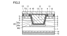
- FIG. 2 is a schematic cross-sectional view taken along line II-II in FIG.
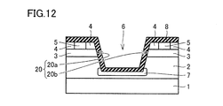
- FIG. 2 is a schematic plan view showing the shape of a groove having a side wall provided in the silicon carbide layer of FIG. 1. It is the elements on larger scale of FIG. 3, and is a figure which shows the asymmetry of a groove
- FIG. 5 is a schematic cross-sectional view taken along line VV in FIG. 4.
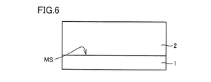
- FIG. 3 is a schematic cross-sectional view for describing a method for manufacturing the semiconductor device shown in FIGS. 1 and 2.
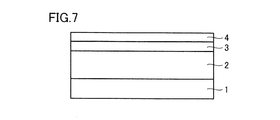
- FIG. 3 is a schematic cross-sectional view for describing a method for manufacturing the semiconductor device shown in FIGS. 1 and 2.
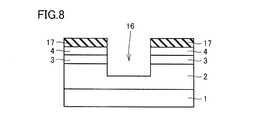
- FIG. 3 is a schematic cross-sectional view for describing a method for manufacturing the semiconductor device shown in FIGS. 1 and 2.
- FIG. 3 is a schematic cross-sectional view for describing a method for manufacturing the semiconductor device shown in FIGS. 1 and 2.
- FIG. 3 is a schematic cross-sectional view for describing a method for manufacturing the semiconductor device shown in FIGS. 1 and 2.
- FIG. 3 is a schematic perspective view for explaining a method for manufacturing the semiconductor device shown in FIGS. 1 and 2.
- FIG. 3 is a schematic cross-sectional view for describing a method for manufacturing the semiconductor device shown in FIGS. 1 and 2.
- FIG. 3 is a schematic cross-sectional view for describing a method for manufacturing the semiconductor device shown in FIGS. 1 and 2.
- FIG. 3 is a schematic cross-sectional view for describing a method for manufacturing the semiconductor device shown in FIGS. 1 and 2.
- FIG. 3 is a schematic cross-sectional view for describing a method for manufacturing the semiconductor device shown in FIGS
- FIG. 3 is a schematic cross-sectional view for describing a method for manufacturing the semiconductor device shown in FIGS. 1 and 2.
- FIG. 5 is a schematic cross-sectional view for explaining a modification of the method for manufacturing the semiconductor device shown in FIGS. 1 and 2.
- FIG. 5 is a schematic cross-sectional view for explaining a modification of the method for manufacturing the semiconductor device shown in FIGS. 1 and 2.
- FIG. 3 is a schematic cross-sectional view showing a modification of the semiconductor device shown in FIGS. 1 and 2. It is a cross-sectional schematic diagram which shows Embodiment 2 of the semiconductor device by this invention.
- FIG. 19 is a schematic cross-sectional view for illustrating the method for manufacturing the semiconductor device shown in FIG. 18.
- FIG. 19 is a schematic cross-sectional view for illustrating the method for manufacturing the semiconductor device shown in FIG. 18.
- FIG. 19 is a schematic cross-sectional view for illustrating the method for manufacturing the semiconductor device shown in FIG. 18.
- FIG. 19 is a schematic cross-sectional view for illustrating the method for manufacturing the semiconductor device shown in FIG. 18.
- FIG. 19 is a schematic cross-sectional view for illustrating the method for manufacturing the semiconductor device shown in FIG. 18.
- FIG. 19 is a schematic cross-sectional view for illustrating the method for manufacturing the semiconductor device shown in FIG. 18.
- FIG. 19 is a schematic cross-sectional view for illustrating the method for manufacturing the semiconductor device shown in FIG. 18.
- FIG. 19 is a schematic cross-sectional view for illustrating the method for manufacturing the semiconductor device shown in FIG. 18.
- FIG. 19 is a schematic cross-sectional view showing a modification of the semiconductor device shown in FIG. 18. It is a partial expanded cross section schematic diagram of the side surface of a silicon carbide layer.
- the semiconductor device in the present embodiment is a vertical MOSFET having a trench gate.
- This semiconductor device has a substrate 1 made of silicon carbide and a silicon carbide layer formed epitaxially on main surface MS of substrate 1.
- the silicon carbide layer has a breakdown voltage holding layer 2 that is an epitaxial layer having an n-type conductivity, a p-type body layer 3 (p-type semiconductor layer 3) that has a p-type conductivity, and an n-type conductivity. It has an n-type source contact layer 4 and a contact region 5 whose conductivity type is p-type.
- the substrate 1 is made of silicon carbide having a single crystal structure of either hexagonal system or cubic system.
- the substrate 1 is provided with a main surface MS having an off angle within 5 degrees from the reference plane.
- the reference plane is a ⁇ 000-1 ⁇ plane, and more preferably a (000-1) plane.
- the reference plane is a ⁇ 111 ⁇ plane in the case of a cubic system.
- the off angle is 0.5 degrees or more.
- the silicon carbide layer is epitaxially formed on the main surface MS of the substrate 1 and has a main surface TS substantially parallel to the main surface MS.
- the groove 6 has a side wall 20a (first side wall) and a side wall 20b (second side wall) facing each other.
- the groove 6 has a tapered shape that widens towards the opening, so that the side walls 20a and 20b) are inclined with respect to each other.
- Each of side walls 20 a and 20 b (generally also referred to as side wall 20) includes a channel region that is a portion on side wall 20 of p type body layer 3.
- Each side wall 20 substantially includes one of ⁇ 0-33-8 ⁇ plane and ⁇ 01-1-4 ⁇ plane in the case of hexagonal system, and substantially ⁇ 100 in the case of cubic system. ⁇ Including the surface.
- each of main surfaces MS and TS is inclined with respect to the reference plane.
- the normal vector CA (FIG. 5) of the reference plane is inclined on the main surface TS toward the off-direction off-direction FF.
- each side wall 20 since each side wall 20 has a specific crystallographic orientation, each side wall 20 is inclined by the amount corresponding to the off angle, compared to the case where the off angle is zero. As a result of this inclination, the angles THa and THb of the side walls 20a and 20b with respect to the main surface TS are different from each other. This difference increases as the off angle of the substrate 1 increases.
- this difference is also limited by limiting the upper limit of the absolute value of the off angle of the substrate 1. Therefore, the length of the channel region provided in each of the side walls 20a and 20b, that is, the difference between the channel lengths LCa and LCb is also limited.
- the absolute value of the difference between the angles THa and Thb is 10 degrees or less.
- the presence of the groove 6 corresponds to the presence of a mesa structure (FIG. 3) made of a silicon carbide layer, when viewed in reverse.
- This mesa structure has a side wall 20 and an upper surface made of a main surface TS surrounded by the side wall 20.
- the shape of the upper surface is hexagonal as shown in FIG. 3 in the case of hexagonal crystal and rectangular or square in the case of cubic crystal.
- the semiconductor device also includes a gate insulating film 8, a gate electrode 9, an interlayer insulating film 10, a source electrode 12, a source wiring electrode 13, a drain electrode 14, and a back surface protective electrode 15.
- the breakdown voltage holding layer 2 is formed on one main surface of the substrate 1.
- a p-type body layer 3 is formed on the breakdown voltage holding layer 2.
- An n-type source contact layer 4 is formed on the p-type body layer 3.
- a p-type contact region 5 is formed so as to be surrounded by the n-type source contact layer 4.
- a gate insulating film 8 is formed on the side wall 20 and the bottom wall of the trench 6. This gate insulating film 8 extends to the upper surface of the n-type source contact layer 4.
- a gate electrode 9 is formed on the gate insulating film 8 so as to fill the inside of the trench 6 (that is, so as to fill a space between adjacent mesa structures).
- the upper surface of the gate electrode 9 has substantially the same height as the upper surface of the portion located on the upper surface of the n-type source contact layer 4 in the gate insulating film 8.
- An interlayer insulating film 10 is formed so as to cover a portion of the gate insulating film 8 extending to the upper surface of the n-type source contact layer 4 and the gate electrode 9.
- an opening 11 is formed so as to expose a part of the n-type source contact layer 4 and the p-type contact region 5.
- a source electrode 12 is formed so as to fill the inside of the opening 11 and to be in contact with a part of the p-type contact region 5 and the n-type source contact layer 4.
- Source wiring electrode 13 is formed to be in contact with the upper surface of source electrode 12 and to extend on the upper surface of interlayer insulating film 10.
- a drain electrode 14 is formed on the back surface of the substrate 1 opposite to the main surface on which the breakdown voltage holding layer 2 is formed.
- the drain electrode 14 is an ohmic electrode.
- a back surface protection electrode 15 is formed on the surface opposite to the surface facing the substrate 1.
- the side wall 20 (side wall of the mesa structure) of the groove 6 is inclined, and the side wall of the silicon carbide that forms the breakdown voltage holding layer 2 is hexagonal. In some cases, it is substantially the ⁇ 0-33-8 ⁇ plane.
- the off-angle relative to the ⁇ 0-33-8 ⁇ plane in the ⁇ 1-100> direction is -3 ° or more and 3 ° or less, more preferably -1 ° or more.
- the surface is 1 ° or less.
- these so-called semipolar side walls can be used as a channel region which is an active region of a semiconductor device.
- these side walls are stable crystal planes, when the side walls are used for the channel region, higher channel mobility is obtained than when other crystal planes (for example, (0001) plane) are used for the channel region.
- the leakage current can be sufficiently reduced and a high breakdown voltage can be obtained.
- a reverse bias is applied between p type body layer 3 and breakdown voltage holding layer 2 having an n conductivity type. It becomes a non-conductive state.
- a positive voltage is applied to the gate electrode 9
- an inversion layer is formed in the channel region in the vicinity of the region in contact with the gate insulating film 8 in the p-type body layer 3.
- the n-type source contact layer 4 and the breakdown voltage holding layer 2 are electrically connected.
- a current flows between the source electrode 12 and the drain electrode 14.
- FIGS. 1 and 2 Next, a method of manufacturing the semiconductor device according to the present invention shown in FIGS. 1 and 2 will be described with reference to FIGS.
- substrate 1 made of silicon carbide is prepared.
- the substrate 1 has a single crystal structure of either hexagonal system or cubic system.
- the substrate 1 is provided with a main surface MS having an off angle within 5 degrees from the above-described reference plane.
- the reference plane is the ⁇ 000-1 ⁇ plane for the hexagonal system and the ⁇ 111 ⁇ plane for the cubic system.
- an epitaxial layer of silicon carbide having n type conductivity is formed on main surface MS of substrate 1.
- the epitaxial layer becomes the breakdown voltage holding layer 2.
- Epitaxial growth for forming the breakdown voltage holding layer 2 is a CVD using, for example, a mixed gas of silane (SiH 4 ) and propane (C 3 H 8 ) as a source gas and using, for example, hydrogen gas (H 2 ) as a carrier gas. (Chemical Vapor Deposition) method. At this time, it is preferable to introduce, for example, nitrogen (N) or phosphorus (P) as an n-type impurity.
- the concentration of the n-type impurity in the breakdown voltage holding layer 2 can be set to, for example, 5 ⁇ 10 15 cm ⁇ 3 or more and 5 ⁇ 10 16 cm ⁇ 3 or less.
- the p-type body layer 3 and the n-type source contact layer 4 are formed by implanting ions into the upper surface layer of the breakdown voltage holding layer 2.
- an impurity having a p-type conductivity such as aluminum (Al) is implanted.
- the depth of the region where the p-type body layer 3 is formed can be adjusted by adjusting the acceleration energy of the implanted ions.
- an n-type source contact layer 4 is formed by ion-implanting an impurity of n-type conductivity into the breakdown voltage holding layer 2 in which the p-type body layer 3 is formed.
- phosphorus or the like can be used as the n-type impurity.
- a mask layer 17 is formed on the upper surface of the n-type source contact layer 4.
- an insulating film such as a silicon oxide film can be used.
- the following steps can be used. That is, a silicon oxide film is formed on the upper surface of the n-type source contact layer 4 using a CVD method or the like. Then, a resist film (not shown) having a predetermined opening pattern is formed on the silicon oxide film by using a photolithography method. Using this resist film as a mask, the silicon oxide film is removed by etching. Thereafter, the resist film is removed. As a result, a mask layer 17 having an opening pattern is formed in a region where the groove 16 shown in FIG. 8 is to be formed.
- etching for example, reactive ion etching (RIE) or ion milling can be used.
- RIE reactive ion etching
- ICP inductively coupled plasma
- RIE inductively coupled plasma
- ICP-RIE using SF 6 or a mixed gas of SF 6 and O 2 as a reaction gas can be used.
- a thermal etching process for exposing a predetermined crystal plane in the breakdown voltage holding layer 2, the p-type body layer 3 and the n-type source contact layer 4 is performed.
- etching thermal etching
- a mixed gas of oxygen gas and chlorine gas as a reaction gas
- the heat treatment temperature is preferably 700 ° C. or higher and 1200 ° C. or lower.
- the lower limit of this temperature is more preferably 800 ° C, and still more preferably 900 ° C.
- the upper limit of this temperature is more preferably 1100 ° C., still more preferably 1000 ° C.
- the etching rate in the thermal etching process for forming the surface including the ⁇ 0-33-8 ⁇ plane, the ⁇ 01-1-4 ⁇ plane, or the ⁇ 100 ⁇ plane can be set to a sufficiently practical value. Therefore, the processing time of the process can be sufficiently shortened.
- the inventors preferably set the ratio of the flow rate of oxygen to the flow rate of chlorine supplied in this thermal etching to be 0.1 or more and 2.0 or less, and more preferably the lower limit of this ratio is 0.25. .
- a plane including the ⁇ 0-33-8 ⁇ plane, the ⁇ 01-1-4 ⁇ plane, or the ⁇ 100 ⁇ plane can be reliably formed.
- the reaction gas may contain a carrier gas in addition to the above-described chlorine gas and oxygen gas.
- a carrier gas for example, nitrogen (N 2 ) gas, argon gas, helium gas or the like can be used.
- the etching rate of SiC is, for example, about 70 ⁇ m / hr.
- silicon oxide (SiO 2 ) is used as the mask layer 17, the selectivity ratio of SiC to SiO 2 can be extremely increased, so that the mask layer 17 made of SiO 2 is substantially not etched during SiC etching. Not etched.
- the crystal plane exposed at the side wall 20 may be substantially a ⁇ 0-33-8 ⁇ plane. That is, in the etching under the conditions described above, the ⁇ 0-33-8 ⁇ plane which is the crystal plane with the slowest etching rate is self-formed as the sidewall 20 of the groove 6. As a result, a structure as shown in FIG. 9 is obtained.
- the crystal plane constituting the side wall 20 may be a ⁇ 01-1-4 ⁇ plane. In the case of a cubic system, the crystal plane constituting the side wall 20 may be a ⁇ 100 ⁇ plane.
- the mask layer 17 is removed by an arbitrary method such as etching. Thereafter, a resist film (not shown) having a predetermined pattern is formed by photolithography so as to extend from the inside of the trench 6 to the upper surface of the n-type source contact layer 4.
- a resist film having an opening pattern formed at the bottom of the groove 6 and a part of the upper surface of the n-type source contact layer 4 is used.
- an impurity having a conductivity type of p type is ion-implanted to form an electric field relaxation region 7 at the bottom of the trench 6, and a conductive region in a partial region of the n-type source contact layer 4.
- a contact region 5 having a p-type is formed. Thereafter, the resist film is removed. As a result, a structure as shown in FIGS. 10 and 11 is obtained.
- the planar shape of the groove 6 is a mesh shape in which the planar shape of the unit cell (the annular groove 6 surrounding one mesa structure) is a hexagonal shape.
- the p-type contact region 5 is disposed substantially at the center of the upper surface of the mesa structure as shown in FIG.
- the planar shape of the p-type contact region 5 is the same as the outer peripheral shape of the upper surface of the mesa structure, and is a hexagonal shape.
- an activation annealing step for activating the impurities implanted by the above-described ion implantation is performed.
- annealing is performed without forming a cap layer on the surface of the epitaxial layer made of silicon carbide (for example, on the side wall of the mesa structure).
- the inventors do not deteriorate the surface properties of the above-described ⁇ 0-33-8 ⁇ plane even if the activation annealing treatment is performed without forming a protective film such as a cap layer on the surface. It was found that sufficient surface smoothness can be maintained.
- the activation annealing step is directly performed by omitting the step of forming the protective film (cap layer) before the activation annealing treatment, which has been conventionally considered necessary.
- the activation annealing step may be performed after the cap layer described above is formed.
- the activation annealing treatment may be performed by providing a cap layer only on the upper surfaces of the n-type source contact layer 4 and the p-type contact region 5.
- a gate insulating film 8 is formed so as to extend from the inside of the trench 6 to the upper surfaces of the n-type source contact layer 4 and the p-type contact region 5.
- gate insulating film 8 for example, an oxide film (silicon oxide film) obtained by thermally oxidizing an epitaxial layer made of silicon carbide can be used.
- a gate electrode 9 is formed on the gate insulating film 8 so as to fill the inside of the trench 6.
- the following method can be used.
- a conductor film to be a gate electrode extending to the inside of the trench 6 and the region on the p-type contact region 5 is formed by sputtering or the like.
- any material such as metal can be used as long as it is a conductive material.
- a portion of the conductor film formed in a region other than the inside of the groove 6 is removed by using an arbitrary method such as etch back or CMP (Chemical Mechanical Polishing).
- CMP Chemical Mechanical Polishing
- an interlayer insulating film 10 (see FIG. 14) is formed so as to cover the upper surface of the gate electrode 9 and the upper surface of the gate insulating film 8 exposed on the p-type contact region 5.
- the interlayer insulating film any material can be used as long as it is an insulating material.
- a resist film having a pattern is formed on the interlayer insulating film 10 by using a photolithography method. In the resist film (not shown), an opening pattern is formed in a region located on the p-type contact region 5.
- the interlayer insulating film 10 and the gate insulating film 8 are partially removed by etching.
- an opening 11 is formed in the interlayer insulating film 10 and the gate insulating film 8.
- a conductor film to be the source electrode 12 is formed so as to fill the inside of the opening 11 and cover the upper surface of the resist film described above.
- the portion of the conductor film formed on the resist film is simultaneously removed (list off).
- the source electrode 12 can be formed by the conductor film filled in the opening 11.
- the source electrode 12 is an ohmic electrode in ohmic contact with the p-type contact region 5 and the n-type source contact layer 4.
- the drain electrode 14 (see FIG. 14) is formed on the back surface side of the substrate 1 (the surface side opposite to the main surface on which the breakdown voltage holding layer 2 is formed).
- the drain electrode 14 any material can be used as long as it can make ohmic contact with the substrate 1. In this way, the structure shown in FIG. 14 is obtained.
- the source electrode 12 contacts the upper surface of the source electrode 12 and extends on the upper surface of the interlayer insulating film 10 (see FIG. 2), and the back surface protection electrode 15 formed on the surface of the drain electrode 14 ( 2) is formed using an arbitrary method such as a sputtering method. As a result, the semiconductor device shown in FIGS. 1 and 2 can be obtained.
- FIGS. 15 and 16 a modification of the method for manufacturing the semiconductor device according to the present invention shown in FIGS. 1 and 2 will be described.
- the steps shown in FIGS. 6 to 8 are performed. Thereafter, the mask layer 17 shown in FIG. 8 is removed. Next, a Si coating 21 (see FIG. 15) made of silicon is formed so as to extend from the inside of the trench 16 to the upper surface of the n-type source contact layer 4.
- silicon carbide is reconfigured in the region in contact with the Si coating 21 on the inner peripheral surface of the groove 16 and the upper surface of the n-type source contact layer 4.
- the silicon carbide reconstructed layer 22 is formed so that the side wall of the groove has a predetermined crystal plane ( ⁇ 0-33-8 ⁇ plane). As a result, a structure as shown in FIG. 15 is obtained.
- the remaining Si film 21 is removed.
- etching using a mixed gas such as HNO 3 and HF can be used.
- the surface layer of the reconstruction layer 22 described above is removed by etching. ICP-RIE can be used as the etching for removing the reconstruction layer 22.
- the groove 6 having the inclined side surface can be formed.
- the semiconductor device shown in FIGS. 1 and 2 can be obtained by performing the steps shown in FIGS. 10 to 14 described above.
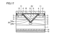
- the semiconductor device shown in FIG. 17 basically has the same configuration as the semiconductor device shown in FIGS. 1 and 2, but the shape of the groove 6 is different from the semiconductor device shown in FIGS. Yes. Specifically, in the semiconductor device shown in FIG. 17, the cross-sectional shape of the groove 6 is V-shaped. From a different point of view, the groove 6 of the semiconductor device shown in FIG. 17 is in a state in which the opposite side surfaces that are inclined with respect to the main surface of the substrate 1 are directly connected at the lower part thereof. An electric field relaxation region 7 is formed at the bottom of the groove 6 (the portion where the lower portions of the opposing side walls are connected to each other).
- the same effects as those of the semiconductor device shown in FIGS. 1 and 2 can be obtained.
- the width of the groove 6 shown in FIG. 17 is the width of the groove 6 shown in FIG. Narrower.
- the semiconductor device shown in FIG. 17 can be smaller in size than the semiconductor device shown in FIG. 2, which is advantageous for miniaturization and higher integration of the semiconductor device.
- the semiconductor device in the first embodiment is a MOSFET including a groove 6 (FIG. 5) having side walls 20a and 20b.
- the semiconductor device in the second embodiment is an insulated gate bipolar transistor (IGBT) having a similar groove 6. The details will be described below.
- the semiconductor device includes a p-type substrate 31 made of silicon carbide, a p-type epitaxial layer 36 serving as a buffer layer made of silicon carbide and having a p-type conductivity, and silicon carbide.
- N-type epitaxial layer 32 as a breakdown voltage holding layer having n-type conductivity, silicon carbide, p-type semiconductor layer 33 corresponding to a well region having p-type conductivity, and silicon carbide
- An n-type source contact layer 34 corresponding to an emitter region having an n-type conductivity, a contact region 35 made of silicon carbide and having a p-type conductivity, a gate insulating film 8, a gate electrode 9, and an interlayer
- the insulating film 10 includes a source electrode 12 corresponding to the emitter electrode, a source wiring electrode 13, a drain electrode 14 corresponding to the collector electrode, and a back surface protection electrode 15.
- the p-type epitaxial layer 36 which is a buffer layer is formed on one main surface MS of the substrate 31.
- An n-type epitaxial layer 32 is formed on the p-type epitaxial layer 36.
- a p-type semiconductor layer 33 is formed on the n-type epitaxial layer 32.
- An n-type source contact layer 34 is formed on the p-type semiconductor layer 33.
- a p-type contact region 35 is formed so as to be surrounded by the n-type source contact layer 34.
- the trench 6 is formed by partially removing the n-type source contact layer 34, the p-type semiconductor layer 33, and the n-type epitaxial layer 32.
- the side wall 20 of the groove 6 is an end surface inclined with respect to the main surface MS of the substrate 31.
- the planar shape of the convex portion surrounded by the inclined end face is a hexagonal shape as in the semiconductor device shown in FIG. Yes.
- a gate insulating film 8 is formed on the side wall 20 and the bottom wall of the groove 6. This gate insulating film 8 extends to the upper surface of the n-type source contact layer 34.
- a gate electrode 9 is formed on the gate insulating film 8 so as to fill the trench 6. The upper surface of the gate electrode 9 has substantially the same height as the upper surface of the portion located on the upper surface of the n-type source contact layer 34 in the gate insulating film 8.
- An interlayer insulating film 10 is formed so as to cover a portion of the gate insulating film 8 extending to the upper surface of the n-type source contact layer 34 and the gate electrode 9.
- the opening 11 is formed so as to expose a part of the n-type source contact layer 34 and the p-type contact region 35.
- Source electrode 12 is formed so as to fill the inside of opening 11 and to be in contact with part of p-type contact region 35 and n-type source contact layer 34.
- Source wiring electrode 13 is formed to be in contact with the upper surface of source electrode 12 and to extend on the upper surface of interlayer insulating film 10.
- the drain electrode 14 and the back surface protection electrode 15 are formed as in the semiconductor device shown in FIGS. Has been.
- sidewall 20 of trench 6 is inclined, and the sidewall 20 forms silicon carbide constituting n-type epitaxial layer 32 and the like.
- the crystal type is hexagonal, it is substantially the ⁇ 0-33-8 ⁇ plane.
- the same effect as the semiconductor device shown in FIG. 1 can be obtained.
- the side wall 20 may be substantially a ⁇ 01-1-4 ⁇ plane.
- the inclined side wall 20 of the groove 6 may be substantially a ⁇ 100 ⁇ plane.
- the substrate 31 passes through the p-type epitaxial layer 36 that is the buffer layer. Holes are supplied to the n-type epitaxial layer 32.
- conductivity modulation occurs in the n-type epitaxial layer 32, and the resistance between the source electrode 12 serving as the emitter electrode and the drain electrode 14 serving as the collector electrode is remarkably reduced. That is, the IGBT is turned on.
- FIGS. 19 to 26 a method for manufacturing the second embodiment of the semiconductor device according to the present invention will be described.
- a substrate 31 having a p-type conductivity and made of silicon carbide is prepared.
- the crystallographic characteristics of the substrate 31 are almost the same as those of the substrate 1 of the first embodiment except for its conductivity type.
- a p-type epitaxial layer 36 of p-type conductivity and made of silicon carbide is formed on the main surface MS of the substrate 31 .
- an n-type epitaxial layer 32 of silicon carbide whose conductivity type is n-type is formed on p-type epitaxial layer 36.
- the n-type epitaxial layer 32 becomes a breakdown voltage holding layer.
- a mixed gas of silane (SiH 4 ) and propane (C 3 H 8 ) is used as a source gas, and a hydrogen gas ( It can be carried out by a CVD method using H 2 ).
- ion implantation is performed on the upper surface layer of the n-type epitaxial layer 32 to form the p-type semiconductor layer 33 and the n-type source contact layer 34.
- a p-type impurity such as aluminum (Al) is ion-implanted.
- the depth of the region where the p-type semiconductor layer 33 is formed can be adjusted by adjusting the acceleration energy of the implanted ions.
- an n-type source contact layer 34 is formed by ion-implanting impurities of n-type conductivity into the n-type epitaxial layer 32 on which the p-type semiconductor layer 33 is formed.
- impurities of n-type conductivity For example, phosphorus or the like can be used as the n-type impurity. In this way, the structure shown in FIG. 20 is obtained.
- a mask layer 17 is formed on the upper surface of the n-type source contact layer 34.
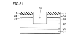
- the n-type source contact layer 34, the p-type semiconductor layer 33, and a part of the n-type epitaxial layer 32 are removed by etching.
- etching method and the like a method substantially similar to the step shown in FIG. 8 can be used. In this way, the structure shown in FIG. 21 is obtained.
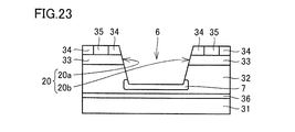
- a thermal etching step for exposing a predetermined crystal plane in the n-type epitaxial layer 32, the p-type semiconductor layer 33, and the n-type source contact layer 34 is performed.
- the conditions for this thermal etching step can be substantially the same as the conditions for the thermal etching step described with reference to FIG.
- the groove 6 having the side wall 20 inclined with respect to the main surface of the substrate 31 can be formed as shown in FIG. In this way, a structure as shown in FIG. 22 is obtained.
- the mask layer 17 is removed by an arbitrary method such as etching. Thereafter, in the same manner as in the step shown in FIG. 10, a resist film (not shown) having a predetermined pattern is formed so as to extend from the inside of the trench 6 to the upper surface of the n-type source contact layer 34. It is formed using a lithography method. As the resist film, a resist film having an opening pattern formed at the bottom of the groove 6 and a part of the upper surface of the n-type source contact layer 34 is used.
- an activation annealing step for activating the impurities implanted by the above-described ion implantation is performed.
- a cap layer is formed particularly on the surface of the epitaxial layer made of silicon carbide (specifically, on the side wall 20 of the groove 6), as in the case of the first embodiment of the present invention already described. Annealing treatment is performed without doing.
- the activation annealing step may be performed after the cap layer described above is formed. Further, for example, the activation annealing process may be performed by providing a cap layer only on the upper surfaces of the n-type source contact layer 34 and the p-type contact region 35.
- a gate insulating film 8 is formed so as to extend from the inside of the trench 6 to the upper surfaces of the n-type source contact layer 4 and the p-type contact region 5.
- the material and forming method of the gate insulating film 8 are the same as the material and forming method of the gate insulating film 8 in FIG. In this way, the structure shown in FIG. 24 is obtained.
- a gate electrode 9 is formed on the gate insulating film 8 so as to fill the inside of the trench 6.
- a formation method of the gate electrode 9 a formation method similar to the formation method of the gate electrode 9 shown in FIG. 13 can be used.
- an interlayer insulating film 10 (see FIG. 26) is formed so as to cover the upper surface of the gate electrode 9 and the upper surface of the gate insulating film 8 exposed on the p-type contact region 35. Any material can be used for the interlayer insulating film 10 as long as it is an insulating material.
- an opening 11 (see FIG. 26) is formed in the interlayer insulating film 10 and the gate insulating film 8. The method for forming the opening 11 is the same as the method for forming the opening in FIG. At the bottom of the opening 11, the p-type contact region 35 and the n-type source contact layer 34 are partially exposed.
- the source electrode 12 is formed from the conductive film filled in the opening 11 by using a method similar to the method described in FIG.
- the source electrode 12 is an ohmic electrode in ohmic contact with the p-type contact region 35 and the n-type source contact layer 34.
- the drain electrode 14 (see FIG. 26) is formed on the back surface side of the substrate 31 (surface side opposite to the main surface on which the n-type epitaxial layer 32 is formed).
- the drain electrode 14 any material can be used as long as it can make ohmic contact with the substrate 31. In this way, the structure shown in FIG. 26 is obtained.
- the semiconductor device shown in FIG. 18 can be obtained.
- the semiconductor device shown in FIG. 27 basically has the same configuration as that of the semiconductor device shown in FIG. 18, but the shape of the groove 6 is different from that of the semiconductor device shown in FIG. Specifically, in the semiconductor device shown in FIG. 27, the cross-sectional shape of the groove 6 is V-shaped like the semiconductor device shown in FIG. An electric field relaxation region 7 is formed at the bottom of the groove 6 (the portion where the lower portions of the opposing side walls are connected to each other). Even with the semiconductor device having such a configuration, the same effect as that of the semiconductor device shown in FIG. 18 can be obtained. Further, in the semiconductor device shown in FIG. 27, since the flat bottom surface as shown in FIG.
- the width of the groove 6 shown in FIG. 27 is the width of the groove 6 shown in FIG. Narrower.
- the semiconductor device shown in FIG. 27 can be smaller in size than the semiconductor device shown in FIG. 18, which is advantageous for miniaturization and higher integration of the semiconductor device.
- the crystal plane constituting the side surface of the groove 6 is the ⁇ 0-33-8 ⁇ plane.
- the ⁇ 0-33-8 ⁇ plane is, as shown in FIG. 28, microscopically, for example, a plane 56a having a plane orientation ⁇ 0-33-8 ⁇ on the side surface of the groove 6 ( A chemically stable surface formed by alternately providing a first surface) and a surface 56b (second surface) connected to the surface 56a and having a surface orientation different from the surface orientation of the surface 56a.
- “microscopic” means that the dimensions are as detailed as at least a dimension of about twice the atomic spacing.
- the surface 56b has a surface orientation ⁇ 0-11-1 ⁇ .
- the length (width) of the surface 56b in FIG. 28 may be, for example, twice the atomic spacing of Si atoms (or C atoms).
- the silicon carbide layer may include a plurality of mesa structures in which the side wall 20 forms a side surface on the main surface located on the opposite side of the surface facing the substrates 1 and 31 as shown in FIGS. Good.
- the surface portion of the silicon carbide layer located between the plurality of mesa structures and continuing to the side wall 20 (the bottom of the groove 6 located between the side surfaces of the plurality of mesa structures) is substantially a ⁇ 000-1 ⁇ plane. Also good.
- the upper surface continuous with the side wall 20 may be substantially a ⁇ 000-1 ⁇ plane.
- the surface portion or the upper surface is substantially a ⁇ 000-1 ⁇ plane when the crystal plane constituting the surface portion or the upper surface is a ⁇ 000-1 ⁇ plane, and the surface It means that the off-angle with respect to the ⁇ 000-1 ⁇ plane in the ⁇ 1-100> direction is a plane of -3 ° or more and 3 ° or less with respect to the crystal plane constituting the partial or upper surface.
- the heat treatment such as the activation annealing described above.
- a step of forming a cap layer on the surface portion or the upper surface of the mesa structure can be omitted for heat treatment such as activation annealing.
- planar shape of the upper surface connected to the side wall 20 in the mesa structure may be a hexagonal shape as shown in FIGS.
- the plurality of mesa structures may include at least three mesa structures.
- the plurality of mesa structures may be arranged such that equilateral triangles are formed by line segments connecting the centers when viewed in plan as shown in FIG. In this case, since the mesa structure can be arranged most densely, more mesa structures can be formed on one substrate 1 and 31. For this reason, as many semiconductor devices as possible using the mesa structure can be formed from one substrate 1, 31.
- the semiconductor device may include a source electrode 12 formed on the upper surface of the mesa structure and a gate electrode 9 formed between the plurality of mesa structures. Good.
- the source electrode 12 and the gate electrode 9 are disposed at positions that are relatively easy to form, it is possible to suppress the manufacturing process of the semiconductor device from becoming complicated.
- the semiconductor device may further include an electric field relaxation region 7 formed between a plurality of mesa structures.
- the electric field relaxation region 7 exists when the drain electrode 14 is formed on the back side of the substrates 1 and 31 (the back side opposite to the main surface where silicon carbide is formed on the substrates 1 and 31).
- the breakdown voltage between the electrode (for example, the gate electrode 9) and the drain electrode 14 between the mesa structures can be increased.
- the semiconductor device manufacturing method may further include a step of forming the source electrode 12 on the upper surface of the mesa structure as shown in FIGS.
- a mesa structure in which the planar shape of the upper surface is a hexagon may be formed as shown in FIG.
- the side wall 20 of the mesa structure can be substantially constituted only by the ⁇ 0-33-8 ⁇ plane. For this reason, the integration degree of a semiconductor device can be improved by using all the side walls 20 on the outer periphery of the mesa structure as a channel region.
- the side wall 20 is formed by a step of forming the mask layer 17 as shown in FIGS. 8 and 21, and a step of forming a mesa structure as shown in FIG. 8 and FIG. 9 or FIG. 21 and FIG. May be included.
- a plurality of mask layers 17 having a hexagonal planar shape may be formed on the main surface of the silicon carbide layer.
- the mask layer 17 may be used as a mask to form a mesa structure having a hexagonal planar shape on the upper surface.
- the position of the mesa structure to be formed (that is, the position of the side wall 20) can be controlled by the pattern position of the mask layer 17. For this reason, the freedom degree of the layout of the semiconductor device formed can be raised.
- the step of forming the side wall 20 includes a step of forming the mask layer 17 and a step of forming the recess (the groove 16 in FIGS. 8 and 21), as shown in FIGS. 9 and the step of forming the mesa structure shown in FIG. 22 may be included.
- a plurality of mask layers 17 having a hexagonal planar shape may be formed on the main surface of the silicon carbide layer at intervals from each other.
- the step of forming the recess (groove 16) by using the mask layer 17 as a mask, the silicon carbide layer exposed between the plurality of mask layers 17 is partially removed to form the main surface of the silicon carbide layer.
- a recess may be formed.
- the mesa structure in which the planar shape of the upper surface is a hexagon may be formed by partially removing the side wall of the groove 16.
- the time for partially removing the side wall of groove 16 (for example, thermal etching) to form the mesa structure can be made shorter than when groove 16 is not previously formed in the silicon carbide layer using mask layer 17 as a mask.
- the mesa structure side wall 20 may be formed in a self-forming manner. Specifically, by performing etching under predetermined conditions on the silicon carbide layer (for example, thermal etching with a mixed gas of oxygen and chlorine as a reaction gas and a heating temperature of 700 ° C. or more and 1200 ° C. or less), The ⁇ 0-33-8 ⁇ plane which is the slowest etching speed in the etching may be expressed in a self-forming manner.
- a silicon film Si film 21
- silicon carbide is present in a state where the Si film 21 exists.
- the SiC reconstruction layer 22 may be formed on the surface, and as a result, the ⁇ 0-33-8 ⁇ surface may be formed. In this case, the ⁇ 0-33-8 ⁇ plane can be stably formed on the side wall 20.
- the mesa structure side wall 20 and the surface portion of the silicon carbide layer (the bottom wall of the groove 6) located between the plurality of mesa structures and connected to the side wall 20 are formed in a self-forming manner. May be.
- the ⁇ 0-33-8 ⁇ plane is exposed as the side wall 20 of the mesa structure by using a method such as the thermal etching or the formation of the SiC reconstruction layer 22 and the bottom wall of the groove 6 is exposed.
- a predetermined crystal plane for example, (0001) plane or (000-1) plane
- a predetermined crystal plane ( ⁇ 0-33-8 ⁇ plane) can be stably formed on the bottom wall of the groove 6 together with the side wall 20.
- the side wall 20 may include an active region as shown in FIGS.
- the active region includes a channel region. In this case, the characteristics such as the reduction of the leakage current and the high breakdown voltage described above can be obtained with certainty.
Landscapes
- Insulated Gate Type Field-Effect Transistor (AREA)
- Electrodes Of Semiconductors (AREA)
- Drying Of Semiconductors (AREA)
- Physics & Mathematics (AREA)
- Engineering & Computer Science (AREA)
- Plasma & Fusion (AREA)
Abstract
Description
主に図1~図3を参照して、本実施の形態における半導体装置は、トレンチゲートを有する縦型MOSFETである。この半導体装置は、炭化珪素からなる基板1と、基板1の主表面MS上にエピタキシャルに形成された炭化珪素層とを有する。炭化珪素層は、導電型がn型であるエピタキシャル層である耐圧保持層2と、導電型がp型であるp型ボディ層3(p型半導体層3)と、導電型がn型であるn型ソースコンタクト層4と、導電型がp型であるコンタクト領域5とを有する。
上記実施の形態1における半導体装置は、側壁20aおよび20bを有する溝6(図5)を含むMOSFETである。実施の形態2における半導体装置は、同様の溝6を有する絶縁ゲートバイポーラトランジスタ(IGBT)である。以下にその詳細について説明する。
ゲート電極9に負の電圧を印加し、当該負の電圧が閾値を超えると、ゲート電極9側方のゲート絶縁膜8に接するp型半導体層33の溝6に対向する端部領域(チャネル領域)に反転層が形成され、エミッタ領域であるn型ソースコンタクト層34と耐圧保持層であるn型エピタキシャル層32とが電気的に接続される。これにより、エミッタ領域であるn型ソースコンタクト層34から耐圧保持層であるn型エピタキシャル層32に電子が注入され、これに対応して基板31からバッファ層であるp型エピタキシャル層36を介して正孔がn型エピタキシャル層32に供給される。その結果、n型エピタキシャル層32に伝導度変調が生じることで、エミッタ電極であるソース電極12-コレクタ電極であるドレイン電極14間の抵抗が著しく低下する。すなわちIGBTがオン状態となる。
Claims (6)
- 六方晶系および立方晶系のいずれかの単結晶構造を有する炭化珪素から作られ、基準面から5度以内のオフ角を有する主表面(MS)が設けられた基板(1)を備え、
前記基準面は、六方晶系の場合は{000-1}面であり立方晶系の場合は{111}面であり、さらに
前記基板の前記主表面上にエピタキシャルに形成された炭化珪素層を備え、
前記炭化珪素層には、互いに対向する第1および第2の側壁(20a、20b)を有する溝(6)が設けられており、前記第1および第2の側壁の各々はチャネル領域を含み、
前記第1および第2の側壁の各々は、六方晶系の場合は実質的に{0-33-8}面および{01-1-4}面のいずれか一方を含み、立方晶系の場合は実質的に{100}面を含む、炭化珪素半導体装置。 - 前記オフ角は0.5度以上である、請求項1に記載の炭化珪素半導体装置。
- 前記主表面に対する前記第1および第2の側壁の各々の傾きの差異が10度以下である、請求項1または2に記載の炭化珪素半導体装置。
- 六方晶系および立方晶系のいずれかの単結晶構造を有する炭化珪素から作られ、基準面から5度以内のオフ角を有する主表面(MS)が設けられた基板(1)を準備する工程を備え、
前記基準面は、六方晶系の場合は{000-1}面であり立方晶系の場合は{111}面であり、さらに
前記基板の前記主表面上にエピタキシャルに炭化珪素層を形成する工程と、
前記炭化珪素層に、互いに対向する第1および第2の側壁(20a、20b)を有する溝(6)を形成する工程とを備え、
前記溝を形成する工程は、
前記炭化珪素層上に、パターンを有するマスク層(17)を設ける工程と、
前記マスク層をマスクとして用いて前記炭化珪素層を部分的にエッチングする工程とを含み、
前記エッチングする工程は、酸素および塩素を含有する反応ガス中で前記炭化珪素層を加熱することによって、前記第1および第2の側壁を形成する工程を含み、前記第1および第2の側壁の各々は、六方晶系の場合は実質的に{0-33-8}面および{01-1-4}面のいずれか一方を含み、立方晶系の場合は実質的に{100}面を含む、炭化珪素半導体装置の製造方法。 - 前記エッチングする工程は、塩素の流量に対する酸素の流量の比率が0.1以上2.0以下となる条件で前記炭化珪素層に前記反応ガスを供給する工程を含む、請求項4に記載の炭化珪素半導体装置の製造方法。
- 前記エッチングする工程は、前記炭化珪素層の温度を700℃以上1200℃以下とする工程を含む、請求項4または5に記載の炭化珪素半導体装置の製造方法。
Priority Applications (3)
| Application Number | Priority Date | Filing Date | Title |
|---|---|---|---|
| EP12831630.4A EP2757588A4 (en) | 2011-09-14 | 2012-08-14 | SILICON CARBIDE SEMICONDUCTOR ELEMENT AND MANUFACTURING METHOD THEREFOR |
| CN201280037159.XA CN103718298B (zh) | 2011-09-14 | 2012-08-14 | 碳化硅半导体器件及其制造方法 |
| KR20137034352A KR20140060264A (ko) | 2011-09-14 | 2012-08-14 | 탄화규소 반도체 장치 및 그 제조 방법 |
Applications Claiming Priority (2)
| Application Number | Priority Date | Filing Date | Title |
|---|---|---|---|
| JP2011200247A JP5699878B2 (ja) | 2011-09-14 | 2011-09-14 | 炭化珪素半導体装置およびその製造方法 |
| JP2011-200247 | 2011-09-14 |
Publications (1)
| Publication Number | Publication Date |
|---|---|
| WO2013038860A1 true WO2013038860A1 (ja) | 2013-03-21 |
Family
ID=47829033
Family Applications (1)
| Application Number | Title | Priority Date | Filing Date |
|---|---|---|---|
| PCT/JP2012/070658 Ceased WO2013038860A1 (ja) | 2011-09-14 | 2012-08-14 | 炭化珪素半導体装置およびその製造方法 |
Country Status (6)
| Country | Link |
|---|---|
| US (1) | US9012922B2 (ja) |
| EP (1) | EP2757588A4 (ja) |
| JP (1) | JP5699878B2 (ja) |
| KR (1) | KR20140060264A (ja) |
| CN (1) | CN103718298B (ja) |
| WO (1) | WO2013038860A1 (ja) |
Cited By (1)
| Publication number | Priority date | Publication date | Assignee | Title |
|---|---|---|---|---|
| WO2015033674A1 (ja) * | 2013-09-06 | 2015-03-12 | 住友電気工業株式会社 | 炭化珪素半導体装置およびその製造方法 |
Families Citing this family (16)
| Publication number | Priority date | Publication date | Assignee | Title |
|---|---|---|---|---|
| JP5764046B2 (ja) * | 2011-11-21 | 2015-08-12 | 住友電気工業株式会社 | 炭化珪素半導体装置の製造方法 |
| JP5806600B2 (ja) * | 2011-11-21 | 2015-11-10 | 住友電気工業株式会社 | 炭化珪素半導体装置の製造方法 |
| US9337271B2 (en) * | 2012-12-28 | 2016-05-10 | Mitsubishi Electric Corporation | Silicon-carbide semiconductor device and manufacturing method therefor |
| JP2014203833A (ja) * | 2013-04-01 | 2014-10-27 | 住友電気工業株式会社 | 炭化珪素半導体装置の製造方法 |
| WO2014178094A1 (ja) | 2013-04-30 | 2014-11-06 | パナソニックIpマネジメント株式会社 | 半導体装置及びその製造方法 |
| JP6036603B2 (ja) | 2013-08-21 | 2016-11-30 | 住友電気工業株式会社 | 炭化珪素半導体装置の製造方法 |
| JP6264211B2 (ja) * | 2014-07-10 | 2018-01-24 | 住友電気工業株式会社 | 半導体装置の製造方法および半導体装置 |
| DE112015003559B4 (de) * | 2014-08-01 | 2024-08-22 | Sumitomo Electric Industries, Ltd. | Epitaxialer Wafer |
| JP6915526B2 (ja) * | 2017-12-27 | 2021-08-04 | 信越半導体株式会社 | 炭化珪素単結晶の製造方法 |
| JP6491784B1 (ja) * | 2018-08-03 | 2019-03-27 | 株式会社日立パワーソリューションズ | 単結晶炭化ケイ素基板、単結晶炭化ケイ素基板の製造方法、および半導体レーザ |
| CN112271215B (zh) * | 2020-11-17 | 2025-01-28 | 国家电网有限公司 | 一种全控型晶闸管芯片及其设计方法 |
| CN117063292B (zh) | 2021-03-22 | 2024-06-07 | 日立能源有限公司 | 功率半导体器件 |
| JP7559881B2 (ja) * | 2022-05-12 | 2024-10-02 | 富士電機株式会社 | 絶縁ゲート型半導体装置 |
| CN115084236B (zh) * | 2022-07-27 | 2022-11-22 | 上海瞻芯电子科技有限公司 | 沟槽栅功率mosfet及其制造方法 |
| US20240274660A1 (en) * | 2023-02-09 | 2024-08-15 | Wolfspeed, Inc. | Power semiconductor devices having non-rectangular semiconductor die for enhanced mechanical robustness and reduced stress and electric field concentrations |
| CN115841952B (zh) * | 2023-02-21 | 2023-06-06 | 湖北九峰山实验室 | 非对称SiC沟槽结构及其制作方法、电子器件 |
Citations (7)
| Publication number | Priority date | Publication date | Assignee | Title |
|---|---|---|---|---|
| JP2006303469A (ja) * | 2005-03-25 | 2006-11-02 | Shindengen Electric Mfg Co Ltd | SiC半導体装置 |
| JP2007080971A (ja) * | 2005-09-12 | 2007-03-29 | Fuji Electric Holdings Co Ltd | 半導体素子およびその製造方法 |
| JP2008235546A (ja) | 2007-03-20 | 2008-10-02 | Denso Corp | 炭化珪素半導体装置およびその製造方法 |
| JP2009523324A (ja) * | 2006-01-10 | 2009-06-18 | クリー・インコーポレーテッド | 炭化珪素ディンプル基板 |
| JP2009289987A (ja) * | 2008-05-29 | 2009-12-10 | Fuji Electric Device Technology Co Ltd | 炭化珪素半導体基板のトレンチ形成方法 |
| JP2011044513A (ja) * | 2009-08-20 | 2011-03-03 | National Institute Of Advanced Industrial Science & Technology | 炭化珪素半導体装置 |
| WO2012017796A1 (ja) * | 2010-08-03 | 2012-02-09 | 住友電気工業株式会社 | 半導体装置およびその製造方法 |
Family Cites Families (53)
| Publication number | Priority date | Publication date | Assignee | Title |
|---|---|---|---|---|
| JP3471473B2 (ja) | 1994-04-06 | 2003-12-02 | 株式会社デンソー | 半導体装置及びその製造方法 |
| JP3531291B2 (ja) | 1994-06-23 | 2004-05-24 | 株式会社デンソー | 炭化珪素半導体装置の製造方法 |
| JP3419163B2 (ja) | 1995-09-06 | 2003-06-23 | 株式会社デンソー | 炭化珪素半導体装置の製造方法 |
| KR100199997B1 (ko) | 1995-09-06 | 1999-07-01 | 오카메 히로무 | 탄화규소 반도체장치 |
| JP3471509B2 (ja) | 1996-01-23 | 2003-12-02 | 株式会社デンソー | 炭化珪素半導体装置 |
| US6133587A (en) | 1996-01-23 | 2000-10-17 | Denso Corporation | Silicon carbide semiconductor device and process for manufacturing same |
| US5882786A (en) | 1996-11-15 | 1999-03-16 | C3, Inc. | Gemstones formed of silicon carbide with diamond coating |
| JPH11251592A (ja) | 1998-01-05 | 1999-09-17 | Denso Corp | 炭化珪素半導体装置 |
| JP2000021849A (ja) | 1998-07-06 | 2000-01-21 | Shin Etsu Handotai Co Ltd | ドライエッチング方法 |
| JP4457432B2 (ja) | 1999-06-17 | 2010-04-28 | 株式会社デンソー | 種結晶とそれを用いた炭化珪素単結晶の製造方法、炭化珪素単結晶体および単結晶製造装置 |
| DE60033829T2 (de) | 1999-09-07 | 2007-10-11 | Sixon Inc. | SiC-HALBLEITERSCHEIBE, SiC-HALBLEITERBAUELEMENT SOWIE HERSTELLUNGSVERFAHREN FÜR EINE SiC-HALBLEITERSCHEIBE |
| WO2001093339A1 (en) | 2000-05-31 | 2001-12-06 | Matsushita Electric Industrial Co. Ltd. | Misfet |
| US20020177321A1 (en) | 2001-03-30 | 2002-11-28 | Li Si Yi | Plasma etching of silicon carbide |
| JP2005056868A (ja) | 2001-06-04 | 2005-03-03 | Matsushita Electric Ind Co Ltd | 炭化珪素半導体装置の製造方法 |
| US20030012925A1 (en) | 2001-07-16 | 2003-01-16 | Motorola, Inc. | Process for fabricating semiconductor structures and devices utilizing the formation of a compliant substrate for materials used to form the same and including an etch stop layer used for back side processing |
| JP2003133434A (ja) | 2001-10-23 | 2003-05-09 | Mitsubishi Electric Corp | 半導体集積回路 |
| JP2003218350A (ja) | 2002-01-22 | 2003-07-31 | Hitachi Ltd | 半導体装置及びその製造方法 |
| JP4593099B2 (ja) | 2003-03-10 | 2010-12-08 | 学校法人関西学院 | 単結晶炭化ケイ素の液相エピタキシャル成長法及びそれに用いられる熱処理装置 |
| US20060249073A1 (en) | 2003-03-10 | 2006-11-09 | The New Industry Research Organization | Method of heat treatment and heat treatment apparatus |
| JP2005167035A (ja) * | 2003-12-03 | 2005-06-23 | Kansai Electric Power Co Inc:The | 炭化珪素半導体素子およびその製造方法 |
| JP4500558B2 (ja) | 2004-02-09 | 2010-07-14 | トヨタ自動車株式会社 | 絶縁ゲート型半導体装置の製造方法 |
| JP4487655B2 (ja) | 2004-04-14 | 2010-06-23 | 株式会社デンソー | 半導体装置の製造方法 |
| EP1752567B1 (en) | 2004-05-27 | 2011-09-14 | Bridgestone Corporation | Process for producing wafer of silicon carbide single-crystal |
| JP5017768B2 (ja) * | 2004-05-31 | 2012-09-05 | 富士電機株式会社 | 炭化珪素半導体素子 |
| ATE459979T1 (de) | 2004-06-30 | 2010-03-15 | Xycarb Ceramics Bv | Verfahren zur oberflächenbehandlung eines metallcarbid-substrates zur verwendung in halbleiterherstellungverfahren und ein metallcarbid-substrat an sich |
| JP2007182330A (ja) | 2004-08-24 | 2007-07-19 | Bridgestone Corp | 炭化ケイ素単結晶ウェハ及びその製造方法 |
| JP4872217B2 (ja) | 2005-02-16 | 2012-02-08 | 富士電機株式会社 | 炭化珪素半導体素子の製造方法 |
| US20060214268A1 (en) | 2005-03-25 | 2006-09-28 | Shindengen Electric Manufacturing Co., Ltd. | SiC semiconductor device |
| JP4986420B2 (ja) | 2005-07-05 | 2012-07-25 | 三菱電機株式会社 | トランジスタ |
| JP2007035823A (ja) | 2005-07-26 | 2007-02-08 | Elpida Memory Inc | トレンチ形成方法、半導体装置の製造方法および半導体装置 |
| JP2007053227A (ja) | 2005-08-18 | 2007-03-01 | Matsushita Electric Ind Co Ltd | 半導体素子およびその製造方法 |
| JP5017855B2 (ja) | 2005-12-14 | 2012-09-05 | 富士電機株式会社 | 半導体装置の製造方法 |
| JP2007243080A (ja) | 2006-03-13 | 2007-09-20 | Fuji Electric Holdings Co Ltd | 半導体装置およびその製造方法 |
| JP5034315B2 (ja) | 2006-05-19 | 2012-09-26 | 三菱電機株式会社 | 半導体装置及びその製造方法 |
| JP2008098593A (ja) | 2006-09-15 | 2008-04-24 | Ricoh Co Ltd | 半導体装置及びその製造方法 |
| US8198675B2 (en) | 2006-11-21 | 2012-06-12 | Sumitomo Electric Industries, Ltd. | Silicon carbide semiconductor device and method of manufacturing the same |
| JP2008135534A (ja) | 2006-11-28 | 2008-06-12 | Toyota Motor Corp | 有底の溝を有する半導体基板の製造方法 |
| JP4046140B1 (ja) | 2006-11-29 | 2008-02-13 | 住友電気工業株式会社 | 炭化珪素半導体装置の製造方法 |
| JP2009005233A (ja) | 2007-06-25 | 2009-01-08 | Sony Corp | コンテンツ再生装置、コンテンツ再生方法、プログラム |
| JP2009170456A (ja) | 2008-01-10 | 2009-07-30 | Sumitomo Electric Ind Ltd | 半導体装置の製造方法 |
| JP2010147222A (ja) | 2008-12-18 | 2010-07-01 | Denso Corp | 炭化珪素半導体装置およびその製造方法 |
| EP2091083A3 (en) | 2008-02-13 | 2009-10-14 | Denso Corporation | Silicon carbide semiconductor device including a deep layer |
| JP5298691B2 (ja) | 2008-07-31 | 2013-09-25 | 住友電気工業株式会社 | 炭化ケイ素半導体装置およびその製造方法 |
| JP5442229B2 (ja) | 2008-09-04 | 2014-03-12 | ローム株式会社 | 窒化物半導体素子の製造方法 |
| JP4544360B2 (ja) | 2008-10-24 | 2010-09-15 | トヨタ自動車株式会社 | Igbtの製造方法 |
| TW201044586A (en) | 2009-03-27 | 2010-12-16 | Sumitomo Electric Industries | Mosfet and method for manufacturing mosfet |
| JP5721351B2 (ja) * | 2009-07-21 | 2015-05-20 | ローム株式会社 | 半導体装置 |
| JP5075280B2 (ja) | 2009-10-23 | 2012-11-21 | パナソニック株式会社 | 半導体装置およびその製造方法 |
| WO2011115294A1 (ja) | 2010-03-16 | 2011-09-22 | 合同会社先端配線材料研究所 | 炭化珪素用電極、炭化珪素半導体素子、炭化珪素半導体装置および炭化珪素用電極の形成方法 |
| JP5741583B2 (ja) | 2010-08-03 | 2015-07-01 | 住友電気工業株式会社 | 半導体装置およびその製造方法 |
| JP5510309B2 (ja) | 2010-12-22 | 2014-06-04 | 株式会社デンソー | 炭化珪素半導体装置およびその製造方法 |
| JP5668576B2 (ja) | 2011-04-01 | 2015-02-12 | 住友電気工業株式会社 | 炭化珪素半導体装置 |
| KR101584023B1 (ko) * | 2011-08-26 | 2016-01-08 | 고쿠리츠다이가쿠호징 나라 센탄카가쿠기쥬츠 다이가쿠인 다이가쿠 | SiC반도체소자 및 그 제조방법 |
-
2011
- 2011-09-14 JP JP2011200247A patent/JP5699878B2/ja active Active
-
2012
- 2012-08-14 KR KR20137034352A patent/KR20140060264A/ko not_active Withdrawn
- 2012-08-14 WO PCT/JP2012/070658 patent/WO2013038860A1/ja not_active Ceased
- 2012-08-14 CN CN201280037159.XA patent/CN103718298B/zh active Active
- 2012-08-14 EP EP12831630.4A patent/EP2757588A4/en not_active Withdrawn
- 2012-09-07 US US13/607,388 patent/US9012922B2/en active Active
Patent Citations (7)
| Publication number | Priority date | Publication date | Assignee | Title |
|---|---|---|---|---|
| JP2006303469A (ja) * | 2005-03-25 | 2006-11-02 | Shindengen Electric Mfg Co Ltd | SiC半導体装置 |
| JP2007080971A (ja) * | 2005-09-12 | 2007-03-29 | Fuji Electric Holdings Co Ltd | 半導体素子およびその製造方法 |
| JP2009523324A (ja) * | 2006-01-10 | 2009-06-18 | クリー・インコーポレーテッド | 炭化珪素ディンプル基板 |
| JP2008235546A (ja) | 2007-03-20 | 2008-10-02 | Denso Corp | 炭化珪素半導体装置およびその製造方法 |
| JP2009289987A (ja) * | 2008-05-29 | 2009-12-10 | Fuji Electric Device Technology Co Ltd | 炭化珪素半導体基板のトレンチ形成方法 |
| JP2011044513A (ja) * | 2009-08-20 | 2011-03-03 | National Institute Of Advanced Industrial Science & Technology | 炭化珪素半導体装置 |
| WO2012017796A1 (ja) * | 2010-08-03 | 2012-02-09 | 住友電気工業株式会社 | 半導体装置およびその製造方法 |
Non-Patent Citations (2)
| Title |
|---|
| H.YANO ET AL.: "Si02/SiC Interface Properties on Various Surface Orientations", MAT. RES. SOC. SYMP. PROC., vol. 742, 2003, pages 219 - 226, XP055142491 * |
| See also references of EP2757588A4 |
Cited By (2)
| Publication number | Priority date | Publication date | Assignee | Title |
|---|---|---|---|---|
| WO2015033674A1 (ja) * | 2013-09-06 | 2015-03-12 | 住友電気工業株式会社 | 炭化珪素半導体装置およびその製造方法 |
| US10014376B2 (en) | 2013-09-06 | 2018-07-03 | Sumitomo Electric Industries, Ltd. | Silicon carbide semiconductor device having a trench with side walls and method for manufacturing same |
Also Published As
| Publication number | Publication date |
|---|---|
| JP2013062392A (ja) | 2013-04-04 |
| US20130062629A1 (en) | 2013-03-14 |
| EP2757588A4 (en) | 2015-06-24 |
| JP5699878B2 (ja) | 2015-04-15 |
| US9012922B2 (en) | 2015-04-21 |
| EP2757588A1 (en) | 2014-07-23 |
| KR20140060264A (ko) | 2014-05-19 |
| CN103718298B (zh) | 2016-08-03 |
| CN103718298A (zh) | 2014-04-09 |
Similar Documents
| Publication | Publication Date | Title |
|---|---|---|
| JP5699878B2 (ja) | 炭化珪素半導体装置およびその製造方法 | |
| JP5741583B2 (ja) | 半導体装置およびその製造方法 | |
| JP5707770B2 (ja) | 半導体装置およびその製造方法 | |
| JP5764046B2 (ja) | 炭化珪素半導体装置の製造方法 | |
| WO2013058037A1 (ja) | 炭化珪素半導体装置およびその製造方法 | |
| JP2013062397A (ja) | 炭化珪素半導体装置の製造方法 | |
| WO2013046924A1 (ja) | 炭化珪素半導体装置 | |
| JP2013110238A5 (ja) | ||
| JP2014241368A (ja) | 炭化珪素半導体装置 | |
| JP2012038771A (ja) | 半導体装置およびその製造方法 | |
| CN104508828A (zh) | 用于制造碳化硅半导体器件的方法 |
Legal Events
| Date | Code | Title | Description |
|---|---|---|---|
| 121 | Ep: the epo has been informed by wipo that ep was designated in this application |
Ref document number: 12831630 Country of ref document: EP Kind code of ref document: A1 |
|
| ENP | Entry into the national phase |
Ref document number: 20137034352 Country of ref document: KR Kind code of ref document: A |
|
| REEP | Request for entry into the european phase |
Ref document number: 2012831630 Country of ref document: EP |
|
| WWE | Wipo information: entry into national phase |
Ref document number: 2012831630 Country of ref document: EP |
|
| NENP | Non-entry into the national phase |
Ref country code: DE |